

Page 1

3
INTRODUCTION
FEATURES
1. General
1) Enhanced IDE interface.
2) Internal 5.25 inch, halfheight CD-R/RW Drive.
3) 2 Mbytes buffer memory.
4) Audio CD like tray loading of a disc without using a caddy.
5) Power loading and power ejecting of a disc. The disc can also be ejected manually.
6) Supports Power saving mode and Sleep mode.
7) Vertical and Horizontal operation.
8) Super Link Function.
2. Supported disc formats
1) Reads and writes data in each CD-ROM, CD-ROMXA, CD-I FMV, Video CD, and CD-EXTRA
2) Reads data in Photo CD (Single and Multi session).
3) Reads and writes standard CD-DA.
4) Reads and writes CD-R discs conforming to “Orange Book Part 2”.
5) Reads and writes CD-RW discs conforming to “Orange Book Parts 3”.
3. Supported write method
1) Disc at once (DAO), Session at once (SAO), Track at once (TAO), Variable packet, Fixed packet, and
Multi-session.
4. Performance
1) Random 110 ms average access time.
2) CD-R Record speed : 4X, 8X, 12X, 16X.
3) CD-RW Record speed : 2X, 4X, 10X.
4) CD-ROM : Max 6,000 KB/s(Max 40x) Sustained Transfer rate.
5) Supports real time error correction and real time layered error correction at each speed.
6) Supports CD-R write operation at each double speed, quadruple speed, eighth speed.
7) Supports CD-RW write operation at double speed and quadruple speed.
8) PIO Mode 4, Multi DMA Mode 2 .
9) Multimedia MPC-3 Spec compliant.
10) Support CD-TEXT read/write.
5. Audio
1) Output 16 bit digital data over ATA interface.
2) 8 Times Digital Filter for CD Audio
3) Software Volume Control
4) Equipped with audio line output and headphone jack for audio CD playback.
5) Front panel Volume Control for Headphone Output.
This service manual provides a variety of service
information.
It contains the mechanical structure of the CDR/RW Drive and the electronic circuits in
schematic form. This CD-R/RW Drive was
manufactured and assembled under our strict
quality control standards and meets or exceeds
industry specifications and standards.
This CD-R/RW drive is an internal drive unit
designed for use with IBM PC, HP Vectra, or
compatible computer. It can write as much as 700
Mbytes of digital data into CD-R/RW disc, and can
read as much as 650 Mbytes of digital data stored
in a CD-ROM, CD-R and CD-RW disc.
This CD-R/RW Drive can easily meet the
upcoming MPC level 3 specification, and its
Enhanced Intelligent Device Electronics (E-IDE)
and ATAPI interface allows Plug and play
integration in the majority of today’s PCs without
the need of an additional interface card.
Page 2
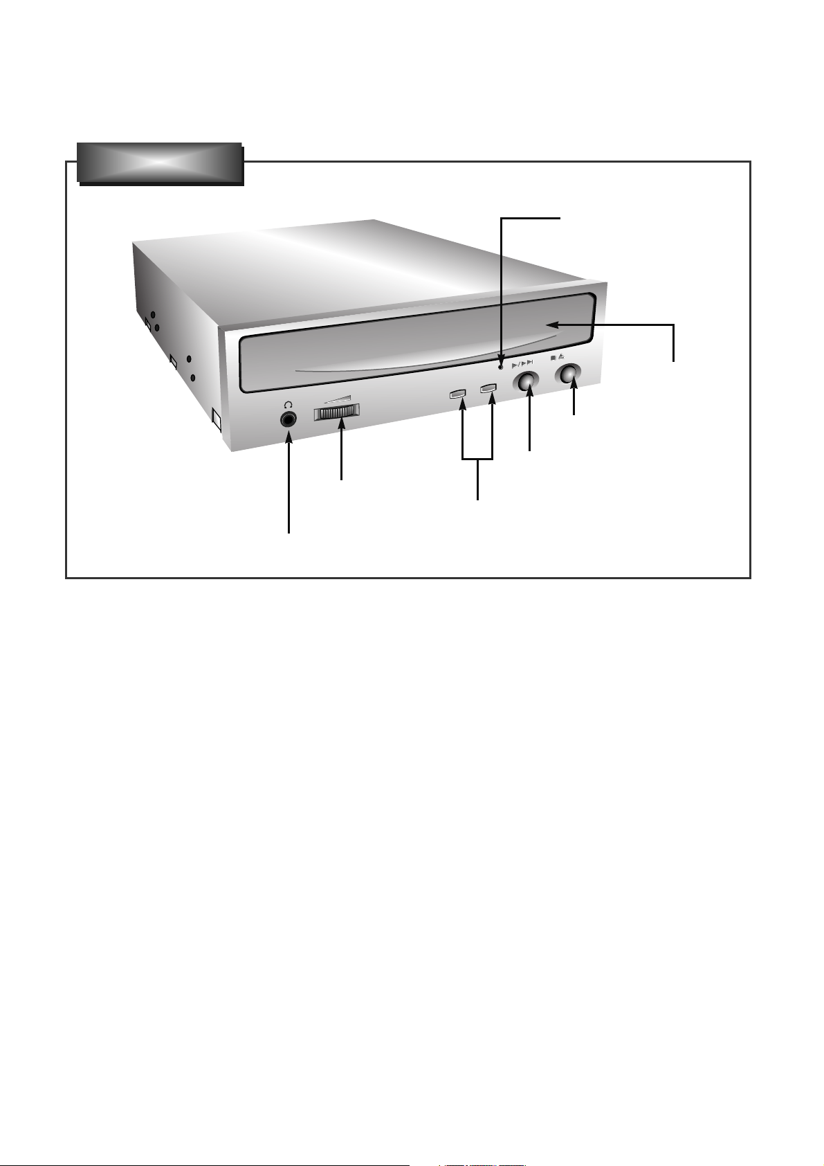
LOCATION OF CUSTOMER CONTROLS
6
1. Disc tray
This is the tray for the disc. Place the disc on the
ejected disc tray, then lightly push the tray (or
push the eject button) and the CD will be loaded.
NOTE: Don’t pull out or push in the disc tray
forcibly. This might cause damage to the loading
section of the drive.
2. Stop/Eject button
This button is pressed to open the CD tray.
This button works only when power is supplied to
the drive.
If an Audio CD is playing, pressing this button will
stop it, and pressing it again will open the tray.
3. Play/Skip button
When an Audio CD is in the disc drawer, pressing
this button will start playing Audio CDs from the
first track. If an Audio CD is playing, pressing this
button will skip to the next track.
4. Emergency Eject Hole
Insert a paper clip here to eject the Disc tray
manually or when there is no power.
5. Volume control
This is used to adjust the output volume of the
headphone jack. It can’t be used to adjust the
output volume for the audio output connectors on
the rear panel.
NOTE : Turn the volume down before turning on
the power. Sudden loud noises can damage your
hearing.
6. Headphone jack
This jack is for connecting headphones or minispeakers.
7. Drive activity indicators
Two colored LEDs are used to indicate the
operation of CD-R/RW Drive.
(1) Read
The orange color is displayed when the spindle
motor begins the Spin up operation: accessing
data, reading data, playing Audio, and up loading
tray.
(2) Write
The green color is flashed during disc writing
sessions.
READ
READ
WRITE
WRITE
Headphone Jack
Volume
Control
Drive Activity Indicators
Play/Skip Button
Stop/Eject Button
Disc Tray
Emergency Eject Hole
Front Panel
Page 3
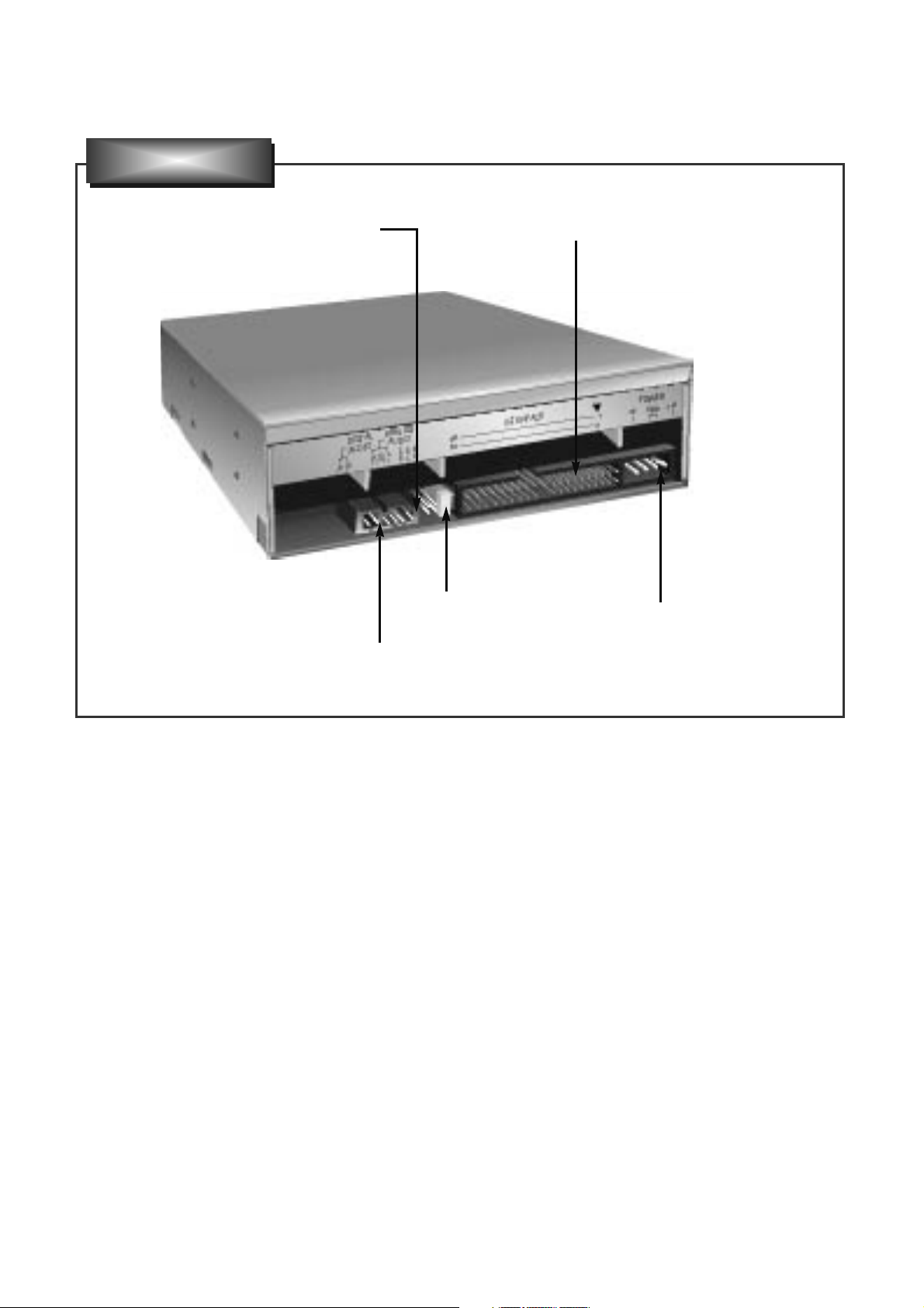
7
1. Power Connector
Connects to the power supply (5-and 12-V DC) of
the host computer.
NOTE : Be careful to connect with the proper
polarity. Connecting the wrong way may damage
the system (and is not guaranteed). Usually this
connector can only be attached one-way.
2. IDE Interface Connector
Connect to the IDE (Integrated Device
Electronics) Interface using a 40-pin flat IDE
cable.
NOTE : Do not connect or disconnect the cable
when the power is on, as this could cause a short
circuit and damage the system. Always turn the
power OFF when connecting or disconnecting the
cable.
3. Jumper Connector
This jumper determines whether the drive is
configured as a master or slave. Changing the
master-slave configuration takes effect after
power-on reset.
4. Analog Audio Output Connector
Provides output to a sound card (analog signal).
Generally you need this to play a regular audio
CD.
5. Digital Audio Output Connector
Provides output to a sound card (digital signal).
Digital Audio Output
Connector
Jumper Connector
Analog Audio Output Connector
IDE Interface Connector
Power Connector
Rear Panel
Page 4
ATIP Absolute Time in Pre-groove. With an additional modulation of the “Wobble”, the “Groove” contains a time
code information.
Wobble The pre-groove in the Disc is not a perfect spiral but is wobbled.
With : – A typical amplitude of 30 nm
– A spatial peried of 54~64 µm
CW Continuous Wave. The laser light output is at a constant level.
DOW Direct Over-Write. The action in which new information is recored over previously recorded information in
CD-RW disc.
Overwrite
The action in which new information is recorded over previously recorded information.
(Pre-)Groove
The guidance track in which clocking and time code information is stored by means of an FM
modulated wobble.
Land Land is characterized in the following way:
When radial signals are concerned,land is defined as the area between the grooves.
When HF signal are concerned,land is defined as the area between the marks(pits) in tangential
direction.
Hybrid Disc A Multisession disc of which the first Session is mastered. On a hybrid disc, recorded and
mastered information may co-exist.
Mastered Information,stored as pits on the disc during the manufacturing process of the disc.
Information (when making the master)
OPC Optimum Power Control. Procedure is determined optimum recording power according to CD-
R/RW Media in recording start step.
ROPC Running OPC. The purpose is to continuously adjust the writing power to the optimum power
that is required.
When the optimum power may change because of changed conditions of disc and change in
operating temperature.
Jitter The 16 value of the time variation between leading and trailing edges of a specific (I3 … I11) pit
or land as measured by Time Interval Analysis.
Deviation The difference between a fixed value of Pit length and Land length.
TOC Table Of Contents : in the Lead-in Area the subcode Q-channel contains information about the
Tracks on the disc.
Packet A method of writing data on a CD in small increments.
Writing Two kinds of packets can be written : Fixed-length and Variable-length.
Write The shape of the HF write signal used to modulate the power of the laser.
Strategy The Write Strategy must be used for recordings necessary for disc measurements.
Information Wobble, ATIP, Disc Identification, Write Power, Speed Range OPC Parameters, etc are
Area recorded in the Information area of CD-RW Disc
Finalization The action in which (partially) unrecorded or logically erased tracks are finished and the Lead-in
and/or Lead-out areas are recorded or overwritten with the appropriate TOC subcode.
Logical Erase
A method to remove information from a disc area by overwriting it with an EFM signal containing
mode 0 subcode
A logically erased area is equivalent to an unrecorded
Physical Erase
The action in which previously recorded information is erased by overwriting with a CW laser
output.
After a Physical Erase action, the erased area on the CD-RW disc is in the unrecorded state
again.
Session
An area on the disc consisting of a Lead-in area, a Program area, a lead-out area.
Multi session
A session that contains or can contain more than one session composed Lead-in and Lead-out
GLOSSARY
10
Page 5
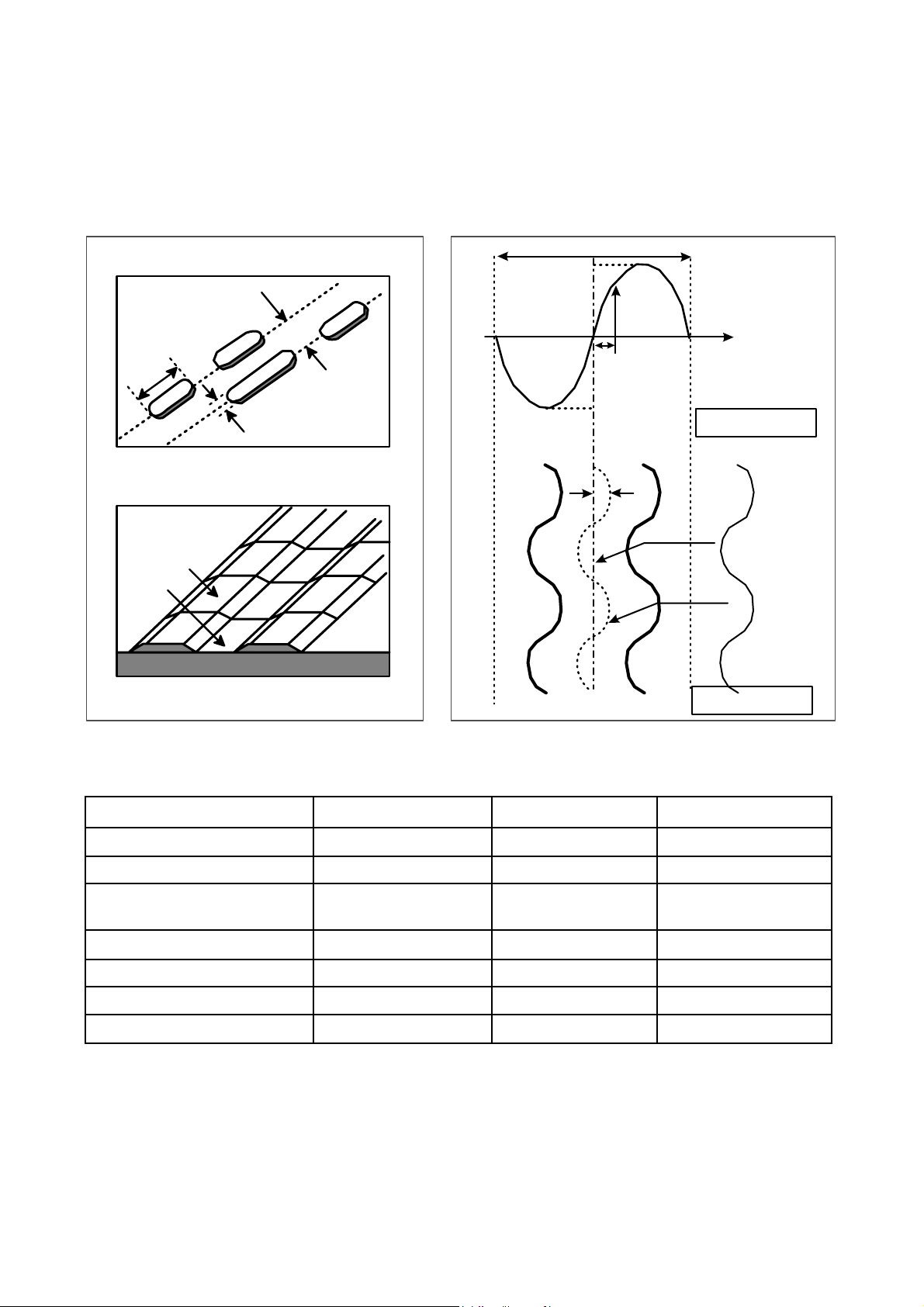
The differences of CD-R/CD-RW discs and General CD-ROM
1. Recording Layer
Recordable CD has a wobbled pre-groove on the surface of disc for laser beam to follow track.
2. Disc Specification
Read-only Disc
CD-R and CD-RW Disc
3~11T
1.6um
0.4~0.5 um
(Pit)Groove
Land
Track pitch(p)
Radial Direction
Iw
A
O
a
a
Groove
Land
Radial Error Signal
The Groove wobble
Average center
Actual center
CD-ROM CD-R CD-RW
Standard Yellow Book Orange Book II Orange Book III
Record Not available Write once Re-writable
I 11/Itop
> 0.6 > 0.6 0.55 > M11> 0.70
(HF Modulation)
Write Laser Power(mW) 10-30 mW 6-25 mW
Read Laser Power(mW) < 0.5 mW < 0.7 mW < 1.0 mW
Jitter < 35 nsec < 35 nsec < 35 nsec
Reflectivity (R
top) 70 % 65 % 15 % ~ 25 %
18
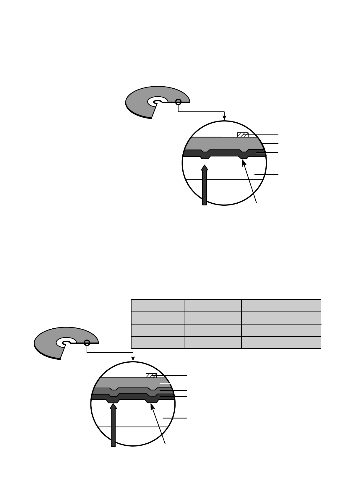
CD-ROM (READ-ONLY DISC)
a=30nm
Page 6
19
3. Disc Materials
1) CD-ROM disc
Laser Beam
Groove
Substrate
(Polycarbonate)
Organic Dye Layer
Reflective Layer
Protective Layer
Label Printing
2) CD-R disc
Pigment Reflective Layer Color
Phtalocyanine Gold/Silver Yellow/White
Cyanine Gold/Silver Dark Green/Bright Green
Az o Gold/Silver Dark Blue
• It is composed of Silver _ colored aluminum plate and Reflective layer.
• Groove (Pit) of aluminum plate make a track.
• Laser wavelength : 780 nm, Laser Power (Read): 0.5mW
• Signal is detected by the
difference of reflective beam
intensity between “pit” and
“Land” on the disc.
• It is so-called WORM (Write Once Read Many) CD.
• It is composed of polycarbonate layer, Organic dye layer, Reflective layer, and Protective
layer.Gold/Silver Reflective layer is used to enhance the reflectivity
• According to the kinds of Organic dye layer, it is divided by Green CD, Gold CD, Blue CD.
• Laser Wavelength : 780 nm, Laser Power (read) : 0.7 mW
• Recording Power : 4x(10~15mW), 8x(14~20mW), 12x(15~30mW, 16x(25~35mW)
• When some part of dye layer is exposed to laser heat, it’s color changs black.Therefore, writing and
reading is enabled by the difference of reflectivity between changed part and unchanged part.
• Polycarbonate layer has Pre_Groove which make a Track.
Laser Beam
Pit
Substrate
(Polycarbonate)
Reflective Layer
Protective Layer
Label Printing
Page 7
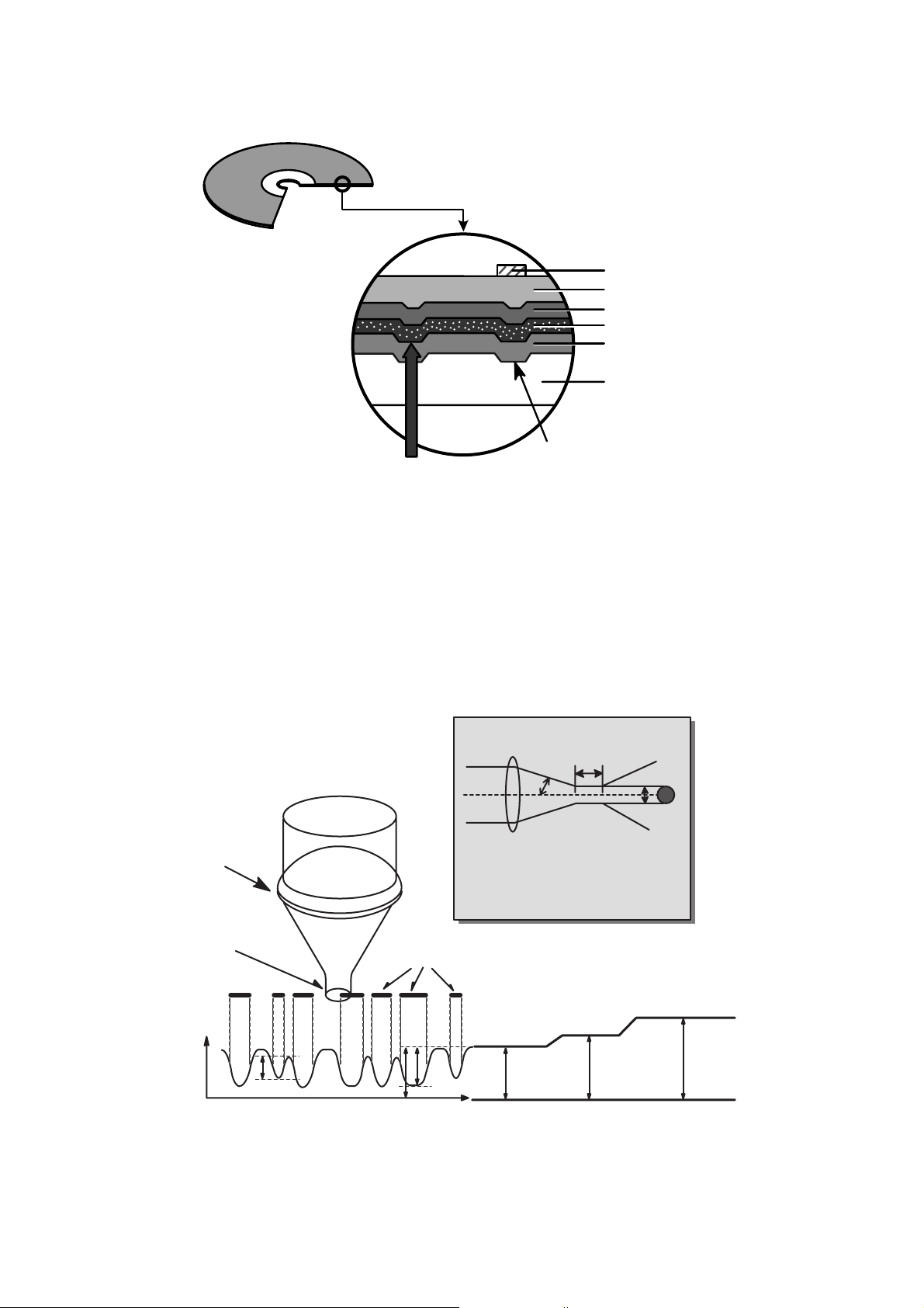
20
33)) CCDD--RRWW DDiisscc
4.
Reading process of Optical Disc
Laser Beam
Groove
Substrate
(Polycarbonate)
Reflective Layer
Dielectric Layer(TL)
Dielectric Layer(UL)
Protective Layer
Label Printing
• It is composed of polycarbonate layer, alloy(silver, arsenic) layer, aluminum reflectivity layer, protective layer.
• An crystalized alloy layer is transformed into noncrystalized by the laser heat. Therefore, writing and reading
is enabled by the difference of reflectivity.
• It is possible to overwrite about 1000 times.
• Laser Wavelength : 780 nm, Laser Power (Read) : 1.0mW
• Recording Power : Erase (4~18mW), Write (6~35mW)
• When disc rewriting, new data is overwritten previously recorded data.
• Polycarbonate layer has a Pre-Groove which make a track.
Lens
H
D
Beam
Spot
Focusing
Lens
Laser Spot
at Constant
Read Intensity
Reflected
Light
Signal
Laser Spot
Position
(Time)
Previously Recorded Marks
Groove Land Mirror
I
3
I
top
I
11
I
G
I
L
I
0
Numerical aperture: NA=nsinθ,
n: Refractive index
Focus depth : H =
λ/
NA
laser spot diameter :
D = λ/NA
2
θ
Page 8
21
5. Writing Process of CD-R Disc
a b c d e f g
a
b
c
d
e
f
g
Incident
Laser
Powe r
(Read)
(Read)
(Write)
Laser Spot
Position
(Time)
a b c d e f g
Laser Spot
Position
(Time)
Laser
Spot
Recorded
Mark
Reflected
Light
Signal
Reflected
Light
Signal
Below "ORP"– Mark Too Short
At Optimum Record Power ("ORP")
Above "ORP" – Mark Too Long
Time
6. Writing process of CD-RW Disc
Write Power
Erase Power
Read Power
Groove
Crystal
Amorphous
Amorphous
Recorded state
(lower reflectivity)
Melting/
quenching
Heating/
gradual cooling
Crystal phase
Erased state
(higher reflectivity)
Page 9
7. Organization of the PCA, PMA and Lead-in Area
1) Layout of CD-ROM disc
22
Center hole Clamping and Label Area Information Area
Lead-in Area
Lead-in Area
Diameter 15 mm
Diameter 46 mm
Diameter 120 mm
Program Area
Read Only Disc
Lead-out Area
Program Area Lead-out Area
Center hole
Clamping and Label Area
Information Area
PCA PMA
Test Area Count Area
Diameter 15 mm
Diameter 45 mm
Diameter 120 mm
Unrecorded Disc
Tsl-00:35:65 Tsl-00:15:05
Tsl-00:13:25
Tsl
99:59:74
00:00:00
in out
Test Area : for performing OPC procedures.
Count Area : to find the usable area immediately in T.A
Tsl : start time of the Lead-in Area, as encoded in ATIP
PMA : Program Memory Area
Disc Center
Disc Center
2) Layout of CD-R/RW disc
Page 10
23
8. Function of PCA and PMA area
1) PCA (Power Calibration Area)
• PCA area is used to determine the correct Laser Power for a disc.
– Method 1 : PCA area is divided by a track.
– Method 2 : The previous Calibration value is referred.
– Method 3 : ROPC is used to determine Laser Power value automatically in data writing.
• CD-R Disc can write maximum 99 Tracks but CD-RW Disc can write unlimited tracks because it has a rewritable
function.
2) PMA (Program Memory Area)
• It has a track information (track No, track Start/End time) of every track before writing completed.
– PMA area has the last written point and the next writable point of a disc.
– In case of CD to CD copy, some writer may not write PMA area.
* When Disc is Finalized,
PMA information is transferred to the Lead_In area so that general Driver can read it.
* Because PCA and PMA area exist before Lead-In area, General CD Player or CD-ROM Drive can’t read
these areas.
9. OPC and ROPC
1) OPC (Optimum Power Control)
• This is the first step of writing process, because CD writer has its own laser power value and media have different
writing characteristics,
– This is determined by the Writing characteristic, speed, temperature, and humidity.
– Laser wavelength is determined by the environmental temperature (775~795nm) and Optical Laser Power is
determined by the test and retry.
• Asymmetry and optimum writing Power
– EFM signal Asymmetry is determined by the writing power.
Therefore, Optical Power which has the same value to the preset power value can be estimated by measuring
HF signal Asymmetry on the PCA area.
• Measurement of Asymmetry
* Parameter setting (Beta) : Using AC coupled HF signal before equalization
Beta = (A1+A2)/(A1-A2)
Time
P << Po
Time
P = Po
HF Signal
A1
0
A2
Time
P >> Po
Page 11
2) ROPC (Running Optimum Power Control)
• Variable primary factor of Optimum Power
– Change of Power sensitivity on the Disc. (limited to 0.05 *Po)
– Wavelength shift of the laser diode due to the operating temperature change.
– Change of the Spot aberration due to the Disc skew,
Substrate thickness, Defocus.
– Change of Disc or Optics conditions due to the long term OPC
==> It is necessary to adjust continuously to obtain the Optimum Power.
• Principle of Running OPC
– To meet the factors mentioned above,
a horizontal _ direction movement of a curve is uesd.
– Beta = f(B-level) = constant on the Recorded Disc
– Procedure of ROPC
a. Reference B-level is determined during OPC Procedure.
b. During Recording, B-level value is controlled to have a close
Reference B-level value.
c. Normalization of B-level is used to eliminate the effect of reflectivity fluctuation.
==> The reflected B-level value is normalized by the disc reflectivity itself.
24
CCDD-- RR // RR WW
Media
Write Strategy
Determination
PCA Test Area
Program Area
PMA Area
Lead-In Area
Lead-out Area
OPC
PCA Count Area
ROPC
* Recording Capacity of CD-R/RW (74Minute Recording media)
• (2048 Byte/Sector) X (75 Sector/Second) X (60 Second/Minute) X 74 Minute
= 681,984,000 Bytes = 682 Mbytes
• But the actual recording capacity is about 650 Mbytes. (according to the ISO 9660 standard, approximately
30 Mbytes are used to make directory structure and volume names.)
Incident recording pulse
Reflected recording pulse
Sampled timing B
11T
Sample B-level (Write Power)
Level B
Sampled at timing B
Pwo decided by OPC
Recording Power
Level B with Pwo
normalized to recording power
Sample Disc Reflectivity
(Read power)
10. Writing Process of DISC
Page 12
INTERNAL STRUCTURE OF THE PICK-UP
1. KRS-302B Circuit Diagram
25
1
2
3
4
5
6
1
2
3
4
5
1
2
3
4
5
6
7
8
9
10
11
12
13
14
15
16
17
18
19
20
21
22
23
24
12
11
10
9
8
7
10
9
8
7
6
R3
VR1
R2
C5
C3
C6
LD
A
11
C
C4
R1
L1
L2
R5
R6
R7
C7
R8
R4
C10 C9 C8
Vcc
2 Axis Actuator
IC1
PDIC
IC2 FPDIC
C1
C2
GND
G
D
C
E
RF
GND
H
A
B
F
Vc
GND
GNDGND
VccVc
BinOUT
PDIN
VOUT
VCC
VREF
VCC
GND
IOUT
IINR
IOUT
IIN2
GND
IIN3
GND
RFREQ
RAMP
GND
ENABLE
GND
OSCEN
WEN3
VCC
WEN2
GND
GND
7
8
9
10
11
12
13
14
15
16
17
18
19
20
21
22
23
24
25
26
27
28
29
30
31
32
6
5
4
3
2
1
FCS -
TRK TRK +
FCS +
GND
PDGND
F
B
A
H
PDVCC
PDVC
G
D
C
E
RF SUM
FPDVCC
FPDVC
FPDGND
FPDO
VCC
VCC
VRDC
VWDC2
VWDC1
GND
GND
OSCEN
WE2
WE1
ENBL
IC3
LD
Driver
Page 13
2. Signal detection of the P/U
1) Focus Error Signal ==> (A+C)-(B+D)
This signal is generated in RF IC (IC401 : MT1506) and controls the pick-up’s up and down to focus on
Disc.
2) Tracking Error Signal (DPP Method) ==> {(A+D)-(B+C)}- kx {(F+H)-(E+G)}
This signal is generated in RF IC (IC401 : MT1506) and controls the pick-up’s left and right shift to find to
track on Disc.
3) RF Signal ==> (A+B+C+D)
This signal is converted to DATA signal in DSP IC (IC301 : MT1505).
26
Pick-Up module
Photo Diode
Tracking
Focusing
Infrared Iaser
k[(F+H) - (E+G)]
(A+D) - (B+C)
(A+D) - (B+C) - k[(F+H) - (E+G)]
Offset
TE
Tp
Sub2
Main
Tp/2
Sub1
Track Center
F, E
D,C
A,B
H,G
Page 14

DESCRIPTION OF CIRCUIT
1. ALPC (Automatic Laser Power Control) Circuit
1-1. ALPC Loop Circuit
27
2Vref
IC403
FPDO
PN401 (P/U)
IC401 MT1506
VWDC2
VWDC1
VRDC
RLDON
WLDON
FVREF
RLDON
RDACX
FPDOX
FPDOX
VRDCO
VRDCO
VRDCX
VWDC1X
VWDC1B
VWDC2B
VWDC2X
VRDCB
VRDC
RREFX
VRDCBSEL
(Level Shift to 2’ FVREF)
WDAC1X
WREF1X
RREFX
FVREF
RWMODE
RDAOUT
VRDCG
RDAC
8
8
"L"
8
"H"
VBDAC
RDACRG
WDA1OUT
RDAON
RREFON
Level Shift
to 0.5V
"L"
"L"
"L"
"H"
"H"
"H"
"L"
"L"
"H"
"H"
"H" : short
"L" : open
"H" : short
"L" : open
"H" : short
"L" : open
"H" "L"
"H" : short
"L" : open
"H" : short
"L" : open
"H" : short
"L" : open
FPDO
RFPDSH
WFPDSH
RLDON
26
27
29
21
21
26
24
28
RFPDSH
WFPDSH
IC201
MT1501
WLDON
10K 4.7K
73
72
19
20
29
20
28
27
26
25
24
23
22
21
54
53
M1
M1
FPDO
M2
M2
M2
VWDC10
M2
M2
M2
M2
D
RREF
V WDC1G
W1DAC
WDAC1G
10
10
RWMODE
WREF1ON
Level Shift
to GND
Level Shift
to GND
S/H
S/H
S/H
WDAC2
WDAC1
VRDC
VRDCN
FPDO
VRDC
RREF
VWDC1N
VWDC1
WREF1
VWDC2N
VWDC2
WREF2
VWDC1
VRDCG
VRDCG
VRDCG
x1/x2
x1/x2
x2, x4, x8, x10
FPDOG
VRDCDAG
VWDC2G
WAPC2ON
WDA2OUT
WAPC2ON
WAPC2ON
W2DAC
WDAC2G
VWDC1
WREF1X
"L"
"H"
"L"
"H"
VWDC2
WREF2X
VWDC2
WREF2X
WLDON
WLDON
WLDONDLY
WLDON
WDAC2X
WDA1ON
WDA2ON
WDA2SEL
WREF2ON
M2
WREF1
M2
WREF2
VWDC1B
RDAC
VWDC20
M2
FPDOG
Gain
VRDC1DAG
VWDC2DAG
Gain
Gain
VRDCDA
0V-VWDC1B
256 Steps
VWDC1DA
0V-VWDC1B
256 Steps
VWDC2DA
0V-VWDC2B
256 Steps
34
VWDC10
33
VWDC20
32
Digital
CKT
(AUX-6)
Page 15

1-2. ALPC(Automatic Laser Power Control) Circuit Operation
ALPC (Automatic Laser Power Control) function in CD-R/RW analog front-end is for constant power level
control purpose. Based on the accurate power sensor(FMD) in PU, APC feedback loop maintains constant
power level against laser diode’s temperature variation.
There are three power control loops in CD-R/RW analog front-end, which are used with different
combination for different applicatioins. Generally, the first APC loop is used for read power control. The 2nd &
3rd APC loop is used for write (or erase) power control for CD-R/RW disc.
The first APC loop amplifies (up to 10x) the FMD signal (FPDO) to enhance the accuracy of read power
control. VRDCG is used to adjust the gain of FMD signal. The built -in 8-bit RDAC is used to set the read power
level.
The 2nd & 3rd APC loop is used for high power control. Both WDAC1 and WDAC2 are 10-bats DAC,
which are used to set the wanted power level. The 3rd APC loop can alos be used as a voltage divider, which
take input from 2nd APC loop (VWDC1B).
Besides, three 8-bit potentiometers (VRDCDA, VWDC1DA, and VWDC2DA) and amplifiers (VRDCDAG,
VWDC1DAG, VWDC2DAG) are used to speed up the transient response of VRDCO, VWDC1O, VWDC2O.
On the other hand, the input signal FPDO after amplification (x2 or x4) will send the MPXOUT2 for
monitoring.
28
Page 16

2. RF Amplifier Circuit
Block Diagram
29
150KHz
150KHz
150KHz
150KHz
(A+C)-(B+D)
K1*(A+C)-(B+D)
FE
FEI
K2*[MPPO-SPPO]
K*E+F+G+H)
A,B,C,D
LPF
(40kHZ)
LPF
(40kHZ)
Gain
Fix
MPPO
MPPO
SPPO
SPPO
TEOS
E,F,G,H
IC401 MT1506
IC301
MT1505
Pick up
KRS-302B
IC201
MT1501
Offset adj
9
8
15
14
16
7
13
10
95
10 122
96
97
98
2
3
4
5
LPF
LPF
ADD
MPPG
LPF
LPF
GAIN
ADD
LPF
x1
x1/x2
ADD
x1/x3
Offset adj
EQRF
Filter
VGA
Offset adj.
Data Slicer
Offset adj
Offset
adj
HPF AGC1/2
Gain
Adj
Gain
Adj
Gain
Adj
Gain
Adj
Gain
Fix
Gain
Fix
CE/MPP
CEI
11 121
TE
TEI
12 120
SBAD
SBAD
14 118
EQRF
RFIS
RFI
88 123
124
ATFG
ATFM
ATFG
60
50
41
LPF
(40K/80K/160K
/320KHz)
LPF LPF AGC3
HPF
VREF
BPF
(22.05KHz)
Page 17

3. Focus/Tracking/Sled Servo Circuit
3-1. Focus, Tracking & Sled Servo Process
30
Focus, Tracking Servo
C
B
D
A
E
F
G
H
Pick- up
A,B,C,D,E,F,G,H
A,B,C,D
Focus Error
Detector
Track Error
Detector
A,B,C,D
E,F,G,H
IC401 MT1506
FE
TE
TE FE
A/D
PARALLEL
DIGITAL
COMPENSATOR
DAC
SLED
COMPENSATOR
STEP1
STEP2
IC301
Servo Control
MT1505
Tracking x5
Focus x5
Tracking Focus ing
Actuator
FEO
TEO
F+
F-
T+
T-
Sled Co ntrol
M
Stepping Control
Logic
SL1+
IC501
M63024FP
SL1-
SL2-
SL2+
IC501 M63024FP
27 115
28 114
108 107
1
2
Page 18

3-2. Focus Servo
The aim of Focus Servo is to maintain the distance between object lens of P/U and disc surface, so that
the detected RF signals (A, B, C, D) can be maximized.
Focus Servo is based on focus error (FE) signal which is generated from focus error detection block in
MT1506(IC401) using Astigmatism Method. Focus gain and path can be changed at the MT1506
according to the disc, and the resulting output (FE) is input to Servo IC (IC301, MT1505).
FE signal after first amplification in MT1505 is A/D converted and input to Digital Equalizer Block, most
important part at the Focus Servo. At the Digital Equalizer, adjustments for Focus Bias and Loop Gain are
performed.
After D/A converted, Focus servo signal is output through FOO port (MT1505, Pin115) and drive Focus
Actuator through the Focus Drive IC (IC501, M63024FP).
3-3. Tracking Servo
The aim of Tracking Servo is to make laser beam trace the data track on disc. Tracking Error (TE) signal
is generated from tracking error detection block in MT1506 (IC401) using DPP (Differential Push-Pull)
Method. DPP method uses not only main beam (A, B, C, D) but side beams (E,F and G, H) for correcting
DC offset generated in Push-Pull method.
The remaining procedures of TE signal processing in MT1505 is similar to Focus Servo.
After D/A converted, Tracking servo signal is output through TRO port (MT1505, Pin114) and drive
Tracking Actuator through the Tracking Drive IC (IC501, M63024FP).
3-4. Sled Servo
The working distance of tracking actuator is too short to cover whole disc radius. Sled Servo make PU
move by little and little so that the laser beam keep tracing the data track on disc continuously when
tracking actuator reaches the working limit.
Another function of Sled Servo is to seek a target point on disc, following user commands.
Sled control signal, STEP 1, 2 is generated in MT1505. STEP 1, 2 are output to sled motor via IC501
(M63024FP).
31
Page 19

4. Spindle Servo Circuit
4-1. Spindle Servo Process
4-2. Spindle Servo
Spindle servo is as followings;
1) Wobble CLV x2, x4, x8, x10, x12, x16 : Blank area in CD-R, CD-RW.
2) CD 15x CAV: Eccentric CD-R/RW.
3) CD 20x CAV: Video CD, CD-DA in CD-ROM/R
4) CD 32x CAV: Recorded area in CD-RW.
5) CD 40x CAV: CD-ROM. Recorded area in CD-R.
– Spindle Servo is controlled by IC201 (MT1501), IC301(MT1505) and servo signal is output via WDMO
(IC201 pin74).
32
C
B
DA
E
F
G
H
Pick- up
IC401 MT1506
Wobble Signal
Generator
RF
SRF
ATFG
Data PLL
Spindle Control
PWM
EQRF
CD EFM
CLV
CAV x40
Hall Sensor
M
Spindl e Motor
IC301
MT1505
IC201 MT1501
IC501 M63024F
6
8
IC510 BA6664FM
WDMO
RDMO
FG
Divider
Wobble Spindle
CLV Control
PWM
106
60
88
124
110
7341
7426
824
120
MATRIX
Current comp.
CTL amp.
Page 20

74
Optical
Pick-up
KRS-302B
PD
VWDC
VRDC
Spindle
Motor
FCS
TRK
SLED
DC Motor
Writing
Strategy
DMO Try control
Address/Data
FEO
TEO
SLO
Servo S/H,
Write S/H Signal
Wobble FG/EFM
Address/Data
RFAC,
RFDC,
FEI, TEI
Data
Laser
Power
Ref.
IC203
AT93C86
2KB
EEPROM
IC302
39SF020A
256KB
Flash ROM
IC401
MT1506E
RF Amp
Wobble
ALPC
DAC
IC301
MT1505E
DSP
Servo
Audio
34.57MHz
IC201
MT1501E
DECODER
ENCODER
ATIP Demodulator
Write Strategy
Write S/H Singnal
I/F
Data
IC202
2MB
SDRAM
H
O
S
T
5V
12V
I/F
Cable
Audio
Mute
Circuit
L,R
Line Out
Audio
L,R
IC501
M63024FP
5Ch Servo DRIVE
3.3V
Reset
BLOCK DIAGRAM
FUNCTIONAL BLOCK DIAGRAM
Page 21

MAJOR IC INTERNAL BLOCK DIAGRAM AND PIN DESCRIPTION
IC401 (MT1506) : CD-R/RW Analog Signal Processor
Block Diagram
33
RFZC1
ATIP
MCLK
ATFM
WBLCLK
ATFG
AGC3C
AGC2C
AGC1C
AGCON
SD ATA
XLAT
SCLK
DIG.
REG.
MPX1
MPX2
RRFX
VCON
RRFX
ADBCO
BCO
ADO
INTAGCON
DEFECT
FPDOX
FELP
TELP
MPPO
SPPO
DRCLP
RFRP
MPX1
MPXOUT1
10-Bit
ADC
TZC
MPX2
MPXOUT2
MPX1
MCLK
MPX2BHC
MPX2PHC
XRST
AVDD1
AVSS1
AVDD2
AVSS2
AVDD3
AVSS3
AVDD4
AVSS4
AVDD5
AVSS5
VREF
P/H
&
B/H
MPX2B
AUX1
ASH
BSH
DSH
ESH
CSH
FSH
GSH
HSH
MPX2
MPX2B
AUX2
DRCMO
ROPCO
RRFXLP
DRCSO
VRDC
VWDC1
VWDC2
VRDCO
VWDC1O
VWDC2O
AUX1
AUX2
APC
VWDC2O
VWDC1O
VRDCO
WREF1
VWDC1
VWDC1N
WREF2
VWDC2
VWDC2N
FVREF
FPDO
RREF
VRDC
VRDCN
RFPDSH
WFPDSH
RLDON
WLDON
FPDOX
RECDIN
RRF
RRFXLP
RECD1
RRF
RRFX
RECD1_DG1
INTAGCON
RECD1-DG1
RRF
OSTCC
EQRF
RFAGCC
EQBIAS
GAINUP
GAINUP
DRCMO
DRCSO
HAVC
INA
INF
ING
INB
GAINUP
INE
INH
INC
IND
SERVSH
WBLSH
ADBCO
ADO
BCO
FEO
MCLK
MPPO
SBADO
SPPO
S/H
&
MATRIX
ROPC
FE
DRCMO2
DRCSO2
CE/MPP
TE
SBAD
TEIN
RFZC
TRON
XTOR
XTAND
SHPC
RFZC1VC
SHBC
SBADLP
DEFECT
SERVO
RFZC1
TZC
DEFECT
Data
Slicer
XDEFM
SLPFN
SLPFP
DEFM
RRF
TE
FE
CE/MPP
SBAD
AVSS
TESTM2
VREF
SBADLP
INA
INB
INC
IND
HAVC
INA
INB
INC
IND
HAVC
WRF
ROPCO
ROPCC
H11T
ADCTG
INA
INB
INC
IND
HAVC
WLDON
DEFECT
EQRF
VCON
GAINUP
EQRF
MCLK
DVDD1
DVSS1
DVDD2
DVSS2
SUBGND
TESTM1
ATFM
FPDO
ROPCO
Page 22

34
• Pin Assignment
Pin Numbers Symbol Type Description
RF Signals & S/H Control Pulses
2 INA Analog Input Input of Main Beam Signal (A)
3 INB Analog Input Input of Main Beam Signal (B)
4 INC Analog Input Input of Main Beam Signal (C)
5 IND Analog Input Input of Main Beam Signal (D)
95 INE Analog Input Input of Side Beam Signal (E)
96 INF Analog Input Input of Side Beam Signal (F)
97 ING Analog Input Input of Side Beam Signal (G)
98 INH Analog Input Input of Side Beam Signal (H)
99 HAVC Analog Input Reference Voltage of Main and Side Beams (2.0V)
56 GAINUP Digital Input (TTL) Gain Control Switch for CD-RW Read Mode
68 SERVSH Digital Input (TTL) S/H Control Pulse of Main and Side Beam Signals
70 WBLSH Digital Input (TTL) S/H Control Pulse of W obble Signal
Focus/Tracking Error & Servo Control Signals
6 DRCMO Analog Output Output of (A+B+C+D) Summing Signal
8 DRCSO Analog Output Output of (E+F+G+H) Summing Signal
7 DRCMO2 Analog Input Re-Input of (A+B+C+D) Summing Signal
9 DRCSO2 Analog Input Re-Input of (E+F+G+H) Summing Signal
10 FE Analog Output Output of Focusing Error Signal
12 TE Analog Output Output of Tracking Error Signal
11 CE/MPP Analog Output Output of Center Error or Main Push-Pull Signal
14 SBAD Analog Output Output of SBAD Signal
13 TEIN Analog Input Input of Out-of-Track Detection Circuit
61 XTOR Digital Output (TTL) Output of Out-of-Track Detection Signal (OR)
62 XTAND Digital Output (TTL) Output of Out-of-Track Detection Signal (AND)
15 SBADLP Analog Input Input of SBAD Signal after LPF for DEFECT Detection
77 DEFECT Digital Output (TTL) Output of DEFECT Signal
16 SHPC Analog Output External Capacitor Connection for Peak Hold of RFRP Signal
17 RFZC1VC Analog Output Reference Voltage for RFRP Peak/Bottom Hold
18 SHBC Analog Output External Capacitor Connection for Bottom Hold of RFRP Signal
78 TRON Digital Input (TTL) Input of Seeking ON Control Signal
64 RFZC Digital Output (TTL) Output of RF Zero Crossing Binary Signal
EQRF (RF Equalizer Filter and Data Slicer) & RRF Circuit
82 EQBIAS Analog Output External Bias Connection for Circuits in EQRF Block
83 OSTCC Analog Output External Capacitor Connection for Offset Cancellation Circuit of
Equalizer Output
84 RFAGCC Analog Output External Capacitor Connection for RF AGC in EQRF Block
88 EQRF Analog Output Output of RF EFM Signal after Equalizer Filter
51 DEFM Digital Output (TTL) Binary Output of EFM Signal after Slicing
52 XDEFM Digital Output (TTL) Binary Output of EFM Inversion Signal after Slicing
80 SLPFP Analog Input Input (+) of Auto Slicing Level
81 SLPFN Analog Input Input (-) of Auto Slicing Level
90 RRF Analog Output Output of Read RF Signal
35 RRFXLP Analog Output Low Pass Output of RRF Signal before Level Shift
86 RECDIN Analog Input Input of RF Signal for Recorded Area Detection
Page 23

35
Pin Numbers Symbol Type Description
63 RECD1 Digital Output (TTL) Output of Recorded Area Detection Signal
ROPC (Running OPC) Related Signals
92 W RF Analog Output Output of Write RF Signal
94 ROPCO Analog Output Output of Amplified B-Level of Write RF Signal
93 ROPCC Analog Input Vin(-) of Amplifier for Sampled B-Level of WRF Signal
55 H11T Digital Input (TTL) S/H Control Pulse of WRF Signal
59 ADCTG Digital Input (TTL) Digital Control Signal for S/H of WRF Signal
APC (Auto Power Control for Laser)
20 FPDO Analog Input Input of Laser Monitor Voltage
19 FVREF Analog Input Reference Voltage of APC Loops (2.0V)
73 RLDON Digital Input (TTL) Laser Diode Control for Read Mode
72 WLDON Digital Input (TTL) Laser Diode Control for Write Mode
54 RFPDSH Digital Input (TTL) S/H Control Pulse for Read APC Mode
53 W FPDSH Digital Input (TTL) S/H Control Pulse for Write APC Mode
27 RREF Analog I/O (1). Input of Power Setting Voltage for Read APC ; (2). Output of
Read APC Reference Voltage Generated by Built-in DAC
29 VRDCN Analog Input Vin(-) of Midcourse Amplifier for Read APC Loop
28 VRDC Analog Output Midcourse Output of Laser Diode Controlling in Read Mode
34 VRDCO Analog Output Output Voltage of Laser Diode Controlling in Read APC
24 WREF1 Analog I/O (1). Input of Power Setting Voltage for W rite APC 1; (2). Output of
Write APC 1 Reference Voltage Generated by Built-in DAC
26 VW DC1N Analog Input Vin(-) of Midcourse Amplifier for Read APC 1
25 VWDC1 Analog Output Midcourse Output of Laser Diode Controlling in Write APC 1
33 VWDC1O Analog Output Output Voltage of Laser Diode Controlling in Write APC 1
21 WREF2 Analog I/O (1). Input of Power Setting Voltage for W rite APC 2; (2). Output of
Write APC 2 Reference Voltage Generated by Built-in DAC
23 VW DC2N Analog Input Vin(-) of Midcourse Amplifier for Write APC 2
22 VWDC2 Analog Output Midcourse Output of Laser Diode Controlling in Write APC 2
32 VWDC2O Analog Output Output Voltage of Laser Diode Controlling in Write APC 2
ATIP (Absolute Time In Pre-groove)
57 AGCON Digital Input (TTL) External ATIP AGC1/2 Enable Pin ( H :AGC ON; L :AGC Reset)
49 AGC1C Analog Output External Capacitor Connection for AGC1 in ATIP Block
48 AGC2C Analog Output External Capacitor Connection for AGC2 in ATIP Block
47 AGC3C Analog Output External Capacitor Connection for AGC3 in ATIP Block
50 ATFM Analog Output Output of Analog Wobble Signal
60 ATFG Digital Output (TTL) Digital Output of Wobble Signal after Slicing
58 WBLCLK Digital Input (TTL) External Clock Input for Wobble BPF (SCF)
MPXOUT (Multiplexer Circuit for Various Signals) and Testing Interface
38 AUX1 Analog Input Auxiliary Input 1 for Signal Monitoring
37 AUX2 Analog Input Auxiliary Input 2 for Signal Monitoring
39 MPXOUT1 Analog Output Multiplexer Output 1 for Signal Monitoring
40 MPXOUT2 Analog Output Multiplexer Output 2 for Signal Monitoring
41 MPX2PHC Analog Output External Capacitor Connection for Peak Hold of MPXOUT2 Signal
42 MPX2BHC Analog Output External Capacitor Connection for Bottom Hold of MPXOUT2
Signal
Serial Interface & Other Digital Control Signals
76 XTAT Digital Input (TTL) Latch Input for Register Setting
Page 24

36
Pin Numbers Symbol Type Description
74 SCLK Digital Input (TTL) Clock Input for Register Setting
75 SDATA Digital I/O (TTL) Data Input/Output for Register Setting
79 XRST Digital Input (TTL) Digital Input for Register Resetting
66 MCLK Digital Input (TTL) Digital Input of Main Clock
Reference Voltage and Power Supplies
44 VREF Analog Input Input of Reference Voltage (2.0V)
46 SUBGND Analog Ground Ground Pin for Substrate Bias of Internal Digital Circuitry
100 AVDD1 Analog Pow er Power Pin for Internal Analog Circuitry (5V)
1 AVSS1 Analog Ground Ground Pin for Internal Analog Circuitry
30 AVDD2 Analog Power Power Pin for Internal Analog Circuitry(5V)
31 AVSS2 Analog Ground Ground Pin for Internal Analog Circuitry
43 AVDD3 Analog Power Power Pin for Internal Analog Circuitry (5V)
45 AVSS3 Analog Ground Ground Pin for Internal Analog Circuitry
87 AVDD4 Analog Power Power Pin for Internal Analog Circuitry (5V)
85 AVSS4 Analog Ground Ground Pin for Internal Analog Circuitry
89 AVDD5 Analog Power Power Pin for Internal Analog Circuitry (5V)
91 AVSS5 Analog Ground Ground Pin for Internal Analog Circuitry
69 DVDD1 Digital Power Power Pin for Internal Digital Circuitry (5V)
71 DVSS1 Digital Ground Ground Pin for Internal Digital Circuitry
65 DVDD2 Digital Power Power Pin for Digital I/O Pads Buffer Circuitry (5V)
67 DVSS2 Digital Ground Ground Pin for Digital I/O Pads Buffer Circuitry
Page 25

IC201(MT1501) : CD-R/RW Encoder/Decoder/Write Strategy Chip
Block Diagram
37
Rel Versi
Host
Interface
Logic
Buffer Memory Controller
DSP
Interface
Logic
uP Interface Logic &
Flash Controller
High Speed
Audio
Playback
Logic
Subcode
FIFO/
Parallelizer
RSPC
Decoding &
Encoding
Logic
CIRC Encoder &
EFM Modulation &
Subcode generator
X'tal Clock
Generator
FM Demodulator &
Bi-Phase data
Demodulator
ATIP Sync Protection &
CRC check &
Target MSF Search
SERVO
Status
Detection
Circuit
EFMPLL
(efmclk
synthesizer)
DAC
Control
Logic
OPC & ROPC
Computation
Unit
Reference
Voltage
Generator &
WDMO Control
Logic
ADC Control Logic
Lasor Power
Control
Logic
From
uP
Wobble
Spindle CLV
Control
Time to Digital
Converter
AK_DECEFM
C2PO
BCK
SD ATA
LRCK
WFCK
SBSO
EXCK
SUB
IPLL
(System
clock
synthesizer)
IPLLVSS
IPLLVDD
TEST_MODE
PRST#
FLAG_[8:0]/UA[6:0]
MISC
Interface
Logic
9
URST
UINT0#
UINT1#
UWR#
URD#
UALE/UA7
UPSEN#/IO3
UA15
UA14
UA8~UA10
FLASH_WE#/IO4
FLASH_OE#/IO5
8
UAD[7:0]
DQML
BA1
BA0
CKE
CLK
12
RA[11:0]
RAS#
ROE#
RWE#
CASH#/RWEH#
CAS#
16
RD[15:0]
ADGO
ASDATA
ALRCK
ABCK
ACLK
DEVSEL
DASP#
CS3FX#
CS1FX#
HA[2:0]
PDIAG#
IOCS16#
INTRQ
DMACK#
IORDY
DIOR#
DIOW#
DMARQ
HD[15:0]
HRST#
3
16
XTALO
XTALI
ADCVSS1
ADCVDD1
ADCVDD2
ADC_IN[2:0]
3
ADCVSS2
REFT
V2REFO
RDMO_IN
WDMO
VREFO
BGVDD
BGVSS
DACVSS
DACVDD
DAC_OUT[3:0]
4
EFMVCOIN
EFMPLLVSS
EFMPLLVDD
DLLVSS
DLLVDD
EFMLPFGND
XTAND/IO0
XTOR
RECD1
SLHOLD
MCLK
RC/IO6
HRFZC
TRON_IN
Write
strategy
Interface
Logic
ASP
Control
Interface
Logic
DECEFM
Wobble
Signal
Interface
Logic
FG
To EFM
Jitter Metter
MIRR/RFZC
XRST
GAINUP
XLAT
XD ATA
XCLK
RLDON
AGCON
FMCK/IO2
FMDT/IO1
ATFG
WSR_CSCEN
WSR_ODON
WSR_WXR
WSR_ENBL
WSR_CMOD
WSR_CFREQ
SERVSH/WG
WBLSH
WFPDSH/EFMCLK
RFPDSH/EFMDATA
WLDON
H11T
DSP_CS#
Page 26

38
PIN DESCRIPTION
Pin Numbers Symbol Type Description
DSP interface
2 C2PO TTL Input, SMT,
50K pull-up
C2 error pointer. Active high when errors occur after CIRC C2
correction.
3 SBSO TTL Input, SMT,
50K pull-up
Subcode serial data input. Supplies the serial Subcode data from
DSP. The Subcode is stored in the order of P–W.
4 W FCK TTL Input, SMT,
50K pull-up
Subcode frame clock input. The active-high signal is used to
indicator the Subcode frame header.
5 SUB TTL Input, SMT,
50K pull-up
Subcode sync input. The active-high signal indicates the position
of a Subcode SYNC pattern.
6 EXCK TTL Input, SMT,
50K pull-up
External clock. This input signal is a clock from the DSP for
reading the serial Subcode data.
8 FG TTL Input, SMT,
50K pull-up
Motor Hall sensor input.
12 TRON_IN TTL Input, SMT,
50K pull-up
On track indicator. The active-high input signal is a indicator used
to point the tracking servo is on track.
13 HRFZC TTL Output,
Slew rate
RF ripper zero crossing signal output.
205 DSP_CS# TTL Output DSP chip select.
206 LRCK TTL Input, SMT, L/R channel indicator. A logical low indicates L channel 16-bit data
and high indicates R channel 16-bit data.
207 SDATA TTL Input, SMT,
50K pull-up
50K pul -up
Serial data input. The serial input is used for receiving the digital
data after CIRC correction of DSP.
208 BCK TTL Input, SMT,
50K pull-up
Bit clock input. The signal clocks the serial data on the SDATA
input. Proper synchronization between LRCK and BCK is
necessary.
Audio Output Interface
9 ABCK TTL Output Audio bit clock output. The signal clocks the serial data on the
ASDATA output. Data on the ASDATA signal shall be latched by
an audio DAC at the rising edge of ABCK.
10 ALRCK TTL Output Audio L/R channel indicator. The signal is the audio left and right
channel clock which indicates the data on ASDATA is from left or
right channel.
11 ASDATA TTL Output Audio serial data output. The signal is the audio serial data output
which supplies the serialized audio samp
le.
194 ACLK TTL I/O DSP main clock input or output. (33.8688M Hz)
The ACLK function is determined by the “AGCON” status during
power-on stage. And can be changed by the “ACLKO UT_SEL” bit
of ATIP “MISCCTL” (0x70) command.
134 ADGO TTL I/O, SMT,
Slew rate,
50K pull-up
Digital Audio Output. The signal is the Digital Audio Output which
supplies the IEC-958 digital audio data.
Alternate function : CPU type selection input during power-on
stage. A logical low input indicates an address/data bus separated
type CPU (eg. H8) is used. A logical high input indicates an
address/data bus multiplexed type CPU (eg. 8051, 8032) is
implemented.
Write Strategy Interface
14 WSR_ENBL CMOS Output Laser diode enable signal output
.
Page 27

39
15 WSR_WXR CMOS Output,
Slew rate
Laser diode write power control output. (Write/Read mode SW
signal)
16 WSR_ODON CMOS Output,
Slew rate
Laser diode over drive control output. (Over drive control SW
signal)
18 WSR_OSCEN CMOS Output,
Slew rate
High frequency modulation enable signal output. (Module control
SW signal)
19 WSR_CMOD CMOS Output,
Slew rate
High frequency modulation mode selection signal output.
20 WSR_CFREQ CMOS Output,
Slew rate
Frequency selection signal output.
RF Interface
22 XLAT CMOS Output Latch signal output for RF register setting.
23 XDATA CMOS Output Data signal output for RF register setting.
24 XCLK CMOS Output Carrier clock signal output for RF register setting.
25 SLHOLD CMOS Output RF slice level hold control signal.
26 RLDON CMOS Output Read laser diode on control signal.
27 W LDON CMOS Output Write laser diode on control signal.
28 WFPDSH
/EFMCLK
CMOS Output,
Slew rate
Sample pulse control signal for RF write APC.
EFM clock output.
29 RFPDSH
/EFMDATA
CMOS Output Sample pulse control signal for RF read APC.
: Recording EFM data output.
31 W BLSH CMOS Output Sample pulse for wobble signal.
32 SERVSH
/WG
CMOS Output Sample pulse for servo signal (main beam/ side beam)
Alternate function
Alternate function
Alternate function : Recording
: Write gate enable signal.
33 DECEFM TTL Input, SMT1Slicing EFM signal input.
35 MCLK CMOS Output
Slew rate
RF main clock output. (34.5744M Hz)
36 MIRR/RFZC TTL Input, SMT RF mirror signal input.
37 RC/IO6 TTL I/O, Slew rate,
50K pull-down
RF radial contrast signal input.
Alternate function : Programmable bi-directional I/O.
38 RECD1 TTL Input, SMT Recorded area detection signal input. Active high when the pick-
up head is in recorded area.
39 XTAND/IO0 TTL I/O, SMT Off track detection signal input.
Alternate function : Programmable bi-directional I/O.
40 XTOR TTL Input, SMT Tracking amplitude signal input.
41 A
TFG TTL Input, SMT Digital wobble signal (22.05
±
1 K H
z) input
42 FMDT/IO1 TTL I/O, SMT,
Slew rate,
50K pull-up
FM digital data (Bi-phase data) i
nput.
44 FMCK/IO2 TTL I/O, Slew rate,
50K pull-up
FM demodulation PLL clock (Bi-phase clock) input.
45 AGCON CMOS I/O
50K pull-down
Wobble AGC circuit enable control output.
Alternate function : ACLK function selection input during
power-on stage. A logical low input indicates ACLK is a 33.8688M
Hz clock input for the clock synchronization of high-speed audio
playback. A logical high input indicates ACLK is as 33.8688M Hz
clock output to provide main clock for DSP chip (MT1505).
46 GAINUP CMOS Output CD-RW media RF gain-up control output.
Page 28

40
47 H11T TTL Output,
Slew rate
EFM 11T indicator for ROPC sampling.
EFMPLL VCO Interface
48 EFMPLLV DD Analog VDD Power pin for EFMPLL VCO circuitry.
49 EFMVCOIN Analog input EFMPLL VCO input.
50 EFMPLLVSS Analog VSS Ground pin for EFMPLL VCO circuitry.
51 EFMLPFGND Analog input EFMPLL LPF ground input.
DLL (Delay Lock Loop) Interface
52 DLLVSS Analog Ground Ground pin for DLL circuitry.
53 DLLVDD Analog Power(5V) Power pin for DLL circuitry.
DAC Interf ace
54 DACVDD Analog Power(5V) Power pin for DAC circuitry.
55 ~ 58 DAC_OUT0 ~
DAC_OUT3
Analog output DA converter output. (10-bit resolution)
59 DACVSS Analog Ground Ground pin for DAC circuitry.
ADC Interface
61, 62, 63 ADC_IN0 ~
ADC_IN2
Analog Input AD converter inputs that want to perform analog to digital
conversion. (8-bit resolution)
66 REFT Analog Output ADC reference ladder top.
64, 65 ADCVDD1,
ADCVDD2
Analog Power(5V) Power pin for ADC circuitry.
60, 67 ADCVSS1,
ADCVSS2
Analog Ground Ground pin for ADC circuitry.
Reference Voltage Interface
68 BGVSS Analog Ground Ground pin for reference voltage generation circuitry.
69 VREFO Analog output 2V reference voltage output.
70 V2REFO Analog output 4V reference voltage output.
71 BGVDD Analog Power(5V) Power pin for reference voltage generation circuitry.
DMO Interface
73 RDMO_IN Analog input Reading path DMO input from DSP.
74 W MDO Analog output Spindle motor PWM control output.
Miscellaneous Interface
76 P
RST# CMOS Input, SMT Power on reset input, low active.
77 TEST_MODE TTL Input,
50K pull-down
Te st mode enable pin, high active. A logical high sets MT1501
enter test mode. An internal pull-down resistor sets MT1501 in
normal operation mode when this pin is floating.
80, 82 FLAG_8,
FLAG_7
TTL I/O,
Slew rate,
50K pull-up
Internal flag monitor output.
2
nd
function : GPIO function.
3
rd
function : External ADC interface
Page 29

41
83, 85, 86,
88~91
FLAG_6/UA6 ~
FLAG_0/UA0
TTL I/O,
Slew rate,
50K pull-up
Internal flag monitor output.
2
nd
function : Address bus bit 6 ~ bit 0 input during address/ data
bus separated type CPU (eg. H8) application.
(FLAG_0 ~ FLAG_6)
3
rd
function : Address bus bit 11 ~ bit 13, bit 16 and bit 17 output
during IDE flash programming mode. (FLAG_0 ~
FLAG_4)
4
th
function : GPIO function.
5
th
function : External ADC interface.
For detail information, please reference to the ”AT I P R e g i s t e r
Definition” manual.
Crystal Interface
78 XTALI Input X`tal input. The working frequency is 34.5744 MHz.
79 XTALO Output X`tal output.
IPLL VCO Interface
104 IPLLV SS Ground Ground pin for IPLL VCO circuitry.
105 IPLLVDD Analog power(5V) Power pin for IPLL VCO circuitry.
Host Interface
92 HRST# TTL Input, SMT,
50K pull-up
Host reset input. The active-low input is referred to as hardware
reset and is used to reset this chip.
113, 110, 108,
106, 101, 99,
96, 94, 93,
95, 98, 100,
103, 107, 109,
111
HD15 ~ HD0 TTL I/O, SMT,
Slew rate, PDR,
PPU, PPD
Host Data bus. This is the 8-bit or 16-bit bi-directional data bus to
the host. The lower 8 bits, HD0–HD7, are used for 8-bit data
transfers. Normally data transfers are 16-bit wide.
Note : All pins except HD7 (no any pull) may be selectively
pull-up or pull-down with 20K resistant.
114 DMARQ TTL Output DMA request. This signal is used for DMA data transfers between
host and device and it shall be asserted by the MT1501 when it is
ready to transfer data to or from the host. The direction of data
transfer is controlled by DIOR# and DIOW#.
115 DIOW# TTL Input, SMT,
50K pull-up
Device I/O write. Stop ultra DMA burst.
For Device I/O Write, this signal is the strobe signal asserted by
the host to write device register or the data port.
For Stop Ultra DMA, this signal shall be negated by the host before
data is transferred in an Ultra DMA burst and is asserted by host
during an Ultra DMA burst to signal the termination of Ultra DMA
burst.
116 DIOR# TTL Input, SMT,
50K pull-up
Device I/O read. Ultra DMA ready. Ultra DMA data strobe.
For Device I/O Read, this signal is the strobe signal asserted by
the host to read device registers or the data port.
For Ultra DMA ready, this is asserted by the host to indicate to the
device that the host is ready to receive Ultra DMA data in burst to
the host.
For Ultra DMA data strobe, this signal is the data out strobe signal
from the host for an Ultra DMA data out burst
Page 30

42
118 IORDY
TTL Output, SMT,
Slew rate, PDR
I/O Channel Ready. Ultra DMA ready. Ultra DMA data strobe.
For I/O channel Ready, this signal is negated to extend the host
transfer cycle of any register read or write when the device is not
able to complete the transfer.
For Ultra DMA Ready, this signal is asserted by the device to
indicate to the host that the device is ready to receive Ultra DMA
data out bursts from the host.
For Ultra DMA data strobe, this is the data in strobe signal from
device for Ultra DMA data in burst to the host.
119 DMACK# TTL Input, SMT,
50K pull-up
DMA Acknowledge. This signal shall be used by the host in
response to DMARQ to acknowledge that it is ready for DMA
transfers.
120 INTRQ TTL I/O,
Slew rate
Device Interrupt. This signal is used to interrupt the host system.
INTRQ is driven only when this chip is addressed. When not
driven, INTRQ is in a high impedance state.
121 IOCS16# TTL Output,
Open-Drain
Device 16-BIT I/O. In PIO transfer modes 0, 1, and 2, IOCS16#
indicates to the host system that the 16-bit data port has been
addressed and that the device is prepared to send or receive a
16-bit data word.
124 PDIAG# TTL I/O,
50K pull-up
Passed Diagnostics. This signal is asserted by Device 1 to
indicate to Device 0 that it has completed diagnostics.
126, 123, 125 HA2, HA0, HA1 TTL Input, SMT,
50K pull-up
Device Address. This is the 3-bit binary coded address provided
by the host to access an ATA register or data.
128 CS1FX# TTL Input, SMT,
50K pull-up
Device Chip Select 0 (for 1Fxh/17xh). This is the chip select signal
from the host to select the Command Block Registers.
129 CS3FX# TTL Input, SMT,
50K pull-up
Device Chip Select 1 (for 3Fxh/37xh). This is the chip select signal
from the host to select the Control Block Registers.
130 DASP# TTL I/O,
50K pull-up
Device Active / Device 1 Present. This is a time-multiplexed signal
that indicates that a device is active, or that Device 1 is present.
132 DEVSEL TTL Input, SMT,
50K pull-up
Device Select. Cleared to zero indicates the driver is master
device. Set to one indicates the driver is slave device.
Buffer Memory Interface
141 BA1 3.3V CMOS
Output,
Slew rate, PDR
SDRAM bank address 1 signal. For SDRAM application only.
When 4-bank SDRAM is used, this pin is used to select bank2 and
bank3 space and musts connect to “BA1” pin of SDRAM.
When two 2-bank SDRAM are used, this pin is used as “Chip
Select” signal output for second SDRAM and musts connect to
“CS#” pin of second SDRAM.
142 BA0 3.3V TTL Output,
Slew rate, PDR
SDRAM bank address 0 signal. For SDRAM application only.
153 DQML 3.3V CMOS
2
Output,
Slew rate, PDR
3
SDRAM low-byte data output mask control signal, high active. For
SDRAM application only.
Page 31

43
154 RWE# 3.3V CMOS
Output,
Slew rate, PDR
RAM Write Enable/RAM Write Enable Low. RAM write enable
signal, low active. When two write enable pins are used, it is the
Write Enable Low signal for writing the lower bytes of a two-WE_
16-bit RAM.
For SDRAM application, this pin is dedicated for “Write Enable”
usage.
155 CAS# 3.3V CMOS
Output,
Slew rate, PDR
Column Address Strobe Low / Column Address Strobe. When two
column address strobe pins are used, this pin is the Column
Address Strobe Low signal for accessing the lower bytes of a
two-CAS# 16-bit RAM. When an 8-bit DRAM is used, this pin shall
be connected to CAS# of the DRAM.
For SDRAM application, this pin is “column address strobe” signal
output connected to SDRAM.
156 RAS# 3.3V CMOS
Output,
Slew rate, PDR
RAM Row Address Strobe. This active-low output is the Row
Address Strobe signal to the RAM.
For SDRAM application, this pin is “row address strobe” signal
output connected to SDRAM.
157 ROE# 3.3V CMOS
Output,
Slew rate, PDR
RAM Output Enable, low active.
For SDRAM application this pin is "Chip Select"signal output
connected to “CS#” pin of SDRAM. When two 2-bank SDRAM are
used, this pin musts connect to “CS#” pin of first SDRAM.
168
CASH#/
RWEH#
3.3V CMOS
Output,
Slew rate, PDR
Column Address Strobe High / RAM Write Enable High. When a
16-bit DRAM is used, this active-low pin functions as Colum
n
address Strobe High for accessing the upper bytes of a two-CAS#
RAM, or as Write Enable High for writing the upper bytes of a
two-WE# RAM.
For SDRAM application, this pin is changed to DQMH and is used
to as SDRAM high-byte data mask control signal, high active.
169 CLK 3.3V CMOS
Output,
Slew rate, PDR
SDRAM clock output. For SDRAM application only.
170 CKE 3.3V CMOS
Output,
Slew rate, PDR
SDRAM clock enable signal output. For SDRAM application only.
158, 159, 160,
161, 162, 164,
165, 167, 143,
144, 145, 146,
147, 148, 150,
151
RD15 ~ RD0 3.3V CMOS I/O,
Slew rate, PDR,
PPU
4
, PPD
5
RAM Data bus. These pins are the bi-directional upper Buffer RAM
data bus to the external buffer memory.
171, 140, 172,
173, 174, 175,
176, 177, 136,
137, 138, 139
RA11~ RA0 3.3V CMOS
Output,
Slew rate, PDR
RAM address bus.
Microcontroller Interface
179 URD# TTL Input, SMT,
50K pull-up
Microcontroller read strobe signal, low active.
.
Page 32

44
180 UWR# TTL Input, SMT,
50K pull-up
Microcontroller write strobe signal, low active.
182 UINT1# TTL Output,
Open-Drain
Interrupt 1 signal output, low active.
183 UINT0# TTL I/O, SMT,
Slew rate,
50K pull-up
Interrupt 0 signal output, low active.
Alternate function : ROM chip select input during
microcontroller flash programming mode. A logical low signal
indicates to select flash ROM data for read cycle. And a logical
high indicates to select non-flash ROM data for read cycle.
184 URST TTL Output Microcontroller reset signal output, high active.
185, 186, 188,
189, 190, 191,
192, 193
UAD0 ~ UAD7 TTL I/O,
Slew rate,
50K pull-up
Microcontroller address/data buses interface. Address and data
are multiplexed by microcontroller and used ALE pin to separate
address and data bus.
195 UALE/UA7 TTL Input, SMT,
50K pull-up
Address latch enable input, high active.
Alternate function : Address bus bit 7 input during address/data
bus separated type CPU (eg. H8) application.
197 UPSEN#/IO3 TTL I/O, SMT,
Slew rate,
50K pull-up
External ROM output port enable signal input, low active.
Alternate function : Programmable bi-directional IO3. For nonflash ROM application, the pin can be programmed as GPIO
function.
198, 200 UA15, UA14 TTL I/O,
Slew rate,
50K pull-up
Address bus bit 15 and14 input.
Alternate function : Address bus bit 15 and 14 output during
IDE flash programming mode.
199 FLASH_WE#
/IO4
TTL I/O,
Slew rate,
50K pull-up
Flash memory write enable signal output, low active.
Alternate function : Programmable bi-directional IO4. For nonflash ROM application, the pin can be programmed as GPIO
function.
201, 202, 204 UA8, UA9,
UA10
TTL I/O,
Slew rate,
50K pull-up
Address bus bit 10, 9 and 8 input.
Alternate function : Address bus bit 10, 9 and 8 output during
IDE flash programming mode.
203 FLASH_OE#
/IO5
TTL I/O,
Slew rate,
50K pull-up
Flash memory output enable signal output, low active.
Alternate function : Programmable bi-directional IO5. For nonflash ROM application, the pin can be programmed as GPIO
function.
Power Supply
7, 30, 43,
84,187
DGND Ground Ground pin for general pad buffer circuitry.
1, 34, 87, 196 DVDD Power (5V) Power pin for general pad buffer circuitry.
21, 133, 181 DVDD3 Power (3.3V) Power pin for internal digital circuitry.
17, 81, 131, 178 DGND Ground Ground pin for internal digital circuitry.
152, 166 DVDD3 Power (3.3V) Power pin for RAM pad buffer circuitry.
149, 163 DGND Ground Ground pin for RAM pad buffer circuitry.
97, 112,
122,135
DGND Ground Ground pin for Host pad buffer circuitry.
102, 117, 127 DVDD Power (5V) Power pin for Host pad buffer circuitry.
72 W_DVDD Power (5V) Power pin for internal fully digital circuitry.
75 W_DGND Ground Ground pin for internal fully digital circuitr
Page 33

IC301 (MT1505) : DSP/Servo Controller/up chip
Block Diagram
45
Data
Slicer
Circuit
RFRP
Circuit
Servo
ADC
Sync
Protection
EFM & Q-code
Demodulation
Data PLL
CLV& ZoneCLV & TrueCAV Control
Audio
Processing
Unit
CIRC Error
Correction
8032
Micro processor
X’tal Clock
Generator
Over-sampling
Digital Filter
Varipitch
Clock
Generator
DAC &
LPF
Subcode
FIFO/
Parallelizer
PDM &
PWM
DAC
Mega
Interface
and
GPIO
Control
ADCVDD
128
127
126
125
124
123
122
121
120
119
SCO
RFDTSLV
ADCVSS
RFI
RFIS
FEI
CSI
TEI
TEZILP
118
SBAD
117
DEFECT
116
PDMVDD
115
FOO
114
TRO
113
PDMVSS
112
PWM2VREF
111
PWMVREF
110
DMO
109
ENDM
108
FMO
107
FMO2
106FG105
PRST_
104
TRCLOSE
102
TROPEN
DVDD3
101
LIMIT_
100
TRAYOUT_
99
TRAYIN_
98
DGND
97
LDE
96
TEST
95
ICEMODE
94
IO3
93
IO2
92
IO1
91
IO0
90
DSEFM/O5
89
UP1_7/MUTE
88
UP1_6/GSW
87
UP1_5/CB
86
UP1_4/APCSW
85
UP1_3
84
UP1_2/AKXRST
83
UP1_1
82
PLAY_
81
EJECT_
80
UP3_5/UT0
79
UP3_4/UT0
78
UP3_1/UTXD
77
UP3_0/URXD
76
DGND
75
UXI/O4
74
DVDD5
73
UA7/OI5
72
UA6/OI4
71
UA5/OI3
70
UA4/OI2
69
UA3/OI1
68
IA2/OI1
67
UA1/O9
66
UA0/O8
65
64
DACVDD
LO
63
DACVREF
62RO61
DACVSS
60
VPVSS
59
VCOCIN
58
VPVDD
57
UP3_7/URD_
56
UP3_6/UWR_
55
DVDD3
54
UP3_3/UNIT1_
53
UP3_2/UNIT0_
52
HRST_
51
DGND
50
UP0_0/UAD0
49
UP0_1/UAD1
48
UP0_2/UAD2
47
UP0_3/UAD3
46
UP0_4/UAD4
45
UP0_5/UAD5
44
UP0_6/UAD6
43
UP0_7/UAD7
42
DGND
41
XTALO
40
XTALI
39
DVDD5
38
UALE
37
UPSEN_
36
UP1_0/UA16
35
UP2_7/UA15
34
UP2_6/UA14
33
UP2_0/UA8
32
UP2_1/UA9
31
UP2_2/UA10
30
UP2_3/UA11
29
UP2_4/UA12
28
UP2_5/UA13
27
LRCK
26
SD ATA
25
BCK
24
C2PO
23
SBSO
22
WFCK
21
SBSY
20
EXCK
19
ABCK
18
DGND
17
ALRCK
16
ASDATA
15
TRON
14
DVDD5
13
PLLVDD
12
PDO
11
IREF
10
LPFN
9
LPFO
8
LPIN
7
LPIO
6
PLLVSS
5
VBDPLL
4
RFBIAS
3
HRFZC
2
RFRPSLV
1
RFRO
Page 34

46
•Pin Description
Pin Numbers Symbol Type Description
Data PLL Interface
5 VBDPLL Analog Output Reference voltage.
6 PLLVSS Anlog Ground Ground pin for data PLL and related analog circuitry.
7 LPIO Analog Output The output of VCO integrator.
8 LPIN Analog Input The negative input terminal of VCO integrator.
9 LPFO Analog Output The output of loop filter amplifier.
10 LPFN Analog Input The negative input terminal of loop filter amplifier.
11 IREF Analog Input Current reference input. It generate reference current for data PLL.
Connect an external 15K resistor to this pin and PLLVSS.
12 PDO Analog Output Phase comparator output. Output the phase difference of EFM and
Pck. Sink or (source) a constant current to loop filter over this pin
when phase difference occurs. Otherwise, this pin is high
impedance.
13 PLLVD D Analog Power(5V) Power for data PLL and related analog circuitry.
14 DVDD5 Power (5V) Power pin for analog digital circuitry.
18 DGND Ground Ground pin for analog digital circuitry.
Decoder Interface
15 TRON TTL output, 4mA Seeking On, active high
16 ASDATA TTL input High Audio serial data input,
17 ALRCK TTL input High Audio serial LR input.
19 ABCK TTL input High Audio serial bit clock input.
20 EXCK TTL I/O output ,4mA Subcode data clock. This clock is used for reading/writing
subcode data out through SBSO pin.. Default is output.
21 SBSY TTL output, 4mA Subcode block sync signal. This pin is high when S0 and S1 is
detected.
22 WFCK TTL output, 4mA Frame sync signal.
23 SBSO TTL output, 4mA Subcode P-W data serial output. The subcode data are stored in
internal buffer and wait for EXCK clock to read.
24 C2PO TTL output, 4mA C2 error pointer. Active high after CIRC C2 corrected is serially
output over this pin.
25 BCK CMOS output, 8mA Serial bit clock output.
26 SDATA CMOS output, 8mA Serial data output.
27 LRCK CMOS output, 8mA L/R channel output. A logical low indicates L channel 16-bit data
and high indicates R channel 16-bit data.
90 DSEFM/O5 TTL output, 4mA After data slicer EFM data
Tur bo 8032 Interface
89 ~ 83 UP1_[7:1] TTL I/O, Slew rate
50K pull_up, 4mA
Programmable bi-directional I/O.
80 UP3_5/UT1 TTL I/O, Slew rate
50K pull_up, 4mA
Programmable bi-directional I/O.
Alternate function : T1. Timer 1 input.
79 UP3_4/UT0 TTL I/O, Slew rate
50K pull_up, 4mA
Programmable bi-directional I/O.
Alternate function : T0. Timer 0 input
mer 0 input.
Page 35

47
78 UP3_1
/ UTXD
TTL I/O, Slew rate
50K pull_up, 4mA
Programmable bi-directional I/O.
Alternate function : TXD. Serial transmit data.
77 UP3_0
/ URXD
TTL I/O, Slew rate
50K pull_up, 4mA
Programmable bi-directional I/O.
Alternate function : RXD. Serial receive data.
75 UXI/O4 TTL otuput, Slew
rate, 8mA
Microprocessor clock for ICE mode or general output O4 for non-ice
mode
73~ 66 UA[7:0]
/ O[15:8]
TTL I/O, Slew rate
programmable
Lower address bus output for external device.
Alternate function : Programmable output.
57 UP3_7
/ URD_
TTL I/O, Slew rate
SMT, 50K pull_up,
4mA
Programmable bi-directional I/O.
Alternate function : RD_. Data write signal.
56 UP3_6
/ UWR_
TTL I/O, Slew rate
SMT, 50K pull_up,
4mA
Programmable bi-directional I/O.
Alternate function : W R_. Data write signal.
54 UP3_3
/ UINT1_
TTL I/O, Slew rate
50K pull_up, 4mA
Programmable bi-directional I/O.
Alternate function : INT1_. External interrupt 0.
53 UP3_2
/ UINT0_
TTL I/O, Slew rate
50K pull_up, 4mA
Programmable bi-directional I/O.
Alternate function : INT0_. External interrupt 0.
43 ~ 50 UP0_[7:0]
/ UAD[7:0]
TTL I/O, Slew rate,
programmable
Programmable bi-directional I/O.
Alternate function : AD[7:0]. Lower address/data bus output for
external device.
38 UALE TTL I/O, 50K
pull_up, 4mA
Address latch enable output, active high.
Alternate function : Programmable GPIO.
37 UPSEN_ TTL I/O, 50K
pull_up, 4mA
Programmable store enable output, active low. PSEN_ enables the
external ROM output port.
Alternate function : Programmable output.
36 UP1_0
/ UA16
TTL I/O, Slew rate
50K pull_up, 4mA
Programmable bi-directional I/O.
Alternate function : A16. Address bit 16 output.
35, 34, 28, 29
30, 31, 32, 33
UP2_[7:0]
/ UA[15:8]
TTL I/O, Slew rate
programmable
Programmable bi-directional I/O.
Alternate function : A[15:8]. Upper address bus input/output.
39 DVDD5 Power(5V) Power pin for output pad circuitry.
42 DGND Ground Ground pin for output pad circuitry.
51 DGND Ground Ground pin for internal digital circuitry.
55 DVDD3 Power(3.3V) Power pin for internal digital circuitry.
74 DVDD5 Power(5V) Power pin for output pad circuitry.
76 DGND Ground Ground pin for output pad circuitry.
98 DGND Ground Ground pin for internal digital circuitry.
102 DVDD3 Power(3.3V) Power pin for internal digital circuitry.
Xtal Interface
40 XTALI Input Xtal input. The working frequency is 33.8688 MHz.
41 XTALO Output Xtal output.
Varipitch VCO Interface
58 VPVDD Analog power(5V) Power pin for varipitch VCO circuitry.
59 VCOCIN Analog Input Connect capacitor for compensator loop filter.
Page 36

48
60 VPVSS Ground Ground pin for varipitch VCO circuitry.
Internal Audio Interface
61 DACVSS Ground Ground pin for internal DAC circuitry.
62 RO Analog Output Right channel of audio.
63 DACVREF Analog Output Reference voltage for external audio filter circuit.
64 LO Analog Output Left channel of audio.
65 DACVDD Analog Power(5V) Power pin for internal DAC circuitry.
Reset Interface
52 URST TTL Input, SMT reset input. The active high input is used to reset MT1505.
105 PRST_ TTL Input, SMT Power on reset input, active low.
Extended GPIO Interface
94 ~91 IO3~ IO0 TTL I/O, Slew rate,
50K pull up, 4mA
Programmable GPIO.
Mega Interface
81 EJECT_ TTLpull up input Eject/stop key input, active low.
82 PLAY_ TTL pull up input Play/pause key input, active low.
95 ICEMODE TTL pull down input ICE mode, active high
96 TEST TTL pull down input Test mode, active high
97 LED TTL Output, 4mA
LED control output. Controlled by µP.
99 TRAYIN_ TTL pull up input Tray_is_in input, A logical low indicates the tray is in. Feedback
flag from tray connector.
100 TRAY OUT_ TTL pull up input Tray_is_out input. A logical low indicates the tray is out. Feedback
flag from tray connector.
101 LIMIT_ TTL pull up input Sledge inner limit input, active low.
103 TROPEN PW M/TTL output
Tray open output. Controlled by µP.
104 TRCLOSE PWM/TTL output
Tray close output. Controlled by µP.
Motor and Actuator Driver Interface
106 FG TTL Input, SMT
50K pull-up
Motor Hall sensor input.
107 FMO2 Analog Output Feed motor 2 control. PWM output..
108 FMO Analog Output Feed motor control. PWM output.
109 ENDM TTL Output, 4mA Enable/disable disk motor. A logical high enables disk motor.
110 DMO Analog Output Disk motor control output. PWM output.
111 PW MVREF Analog Input A reference voltage input for PW M circuitry. A typical value of 2.0 v.
112 PWM2VREF Analog Input A reference voltage input for PWM circuitry. A typical value of 4.0 v.
113 PDMVSS Ground Ground for PDM circuitry.
114 TRO Analog Output Tracking servo output. PDM output of tracking servo compensator.
115 FOO Analog Output Focus servo output. PDM output of focus servo compensator
116 PDMVDD Analog Power(5V) Power for PDM circuitry.
Signal Amplifier Interface
117 DEFECT Analog input Hardware detect Defect from Disk
118 SBAD Analog Input Sub beam add input(E+F)
Page 37

49
119 TEZILP Analog Input Tracking error zero crossing low pass input
120 TEI Analog Input Tracking error input.
121 CSI Analog Input Central servo input.
122 FEI Analog Input Focus error input.
123 RFIS Analog Input RF ripple input.
124 RFI Analog Input RF signal input.
125 ADCVSS Ground Ground pin for ADC circuitry.
126 RFDTSLV Analog Output RF data slicer level output.
127 SCO Analog Output Analog slicer current output.
128 ADCVDD Analog Power(5V) Power pin for ADC circuitry.
1 RFRO Analog Output RF ripple detect output
2 RFRPSLV Analog Output RF ripple slice level output.
3 HRFZC Analog Input High frequency RF ripple zero crossing.
4 RFBIAS Analog Input RF ripple bias adjustment input.
Page 38

50
IC501 (M63024FP): Spindle Motor and 5ch Actuator Driver
Block Diagram
Reverse
Detect
120
MATRIX
Logic Logic
FG
Hall Bias
CTL
amp.
CTL
amp.
CTL
amp.
Direction
comp.
Direction
comp.
Direction
comp.
BIAS
Brake select
TSD
Current
comp.
Current
comp.
Current
comp.
FG x3
VM1
RSPUV
W
RSL1
SL1+
SL1-
VM2
RSL2
SL2+
SL2-
MU1
MU2
OCS
5VCC
LOIN+
VM3
LO-
LO+
FO-
FO+
GND
TO-
TO+
TOIN
FOIN
SL2IN
SL1IN
REF
SPIN
HW-
HW+
HV-
HV+
HU-
HU+
FG
ss s s
Frequency
generator
5V power supply
Regulator
Reg
x5
Tracking
x5
Focus
x8
VM1
Page 39

51
• Pin Description
• Channel select function
Terminal
Symbol Terminal function
1 SL1IN Slide control voltage input1
2 SL2IN Slide control voltage input2
3 VM2 Motor Power Supply2(for Slide)
4 RSL2 Slide current sense2
5 SL2+ Slide non-inverted output2
6 SL2- Slide inverted output2
7 GND GND
8 RSL1 Slide current sense1
9 SL1+ Slide non-inverted output1
10 SL1- Slide inverted output1
11 GND GND
12 W Motor drive output W
13 V Motor drive output V
14 U Motor drive output U
15 RSP Spindle current sensie
16 HW- HW- sensor amp. Input
17 HW+ HW+ sensor amp. input
18 HV- HV- sensor amp. input
19 HV+ HV+ sensor amp. input
20 HU- HU- sensor amp. input
21 HU+ HU+ sensor amp. input
Terminal
Symbol Terminal function
22 VM1 Motor Power Supply1 ( for Spindle)
23 HB Bias for Hall Sensor
24 FG Frequency generator output
25 REF Reference voltage input
26 SPIN Spindle control voltage input
27 FOIN Focus control voltage input
28 TOIN Tracking control voltage input
29 GND GND
30 TO- Tracking inverted output
31 TO+ Tracking non-inverted output
32 5VCC 5V Power Supply (for FS, TS)
33 GND GND
34 FO+ Focus non-inverted output
35 FO- Focus inverted output
36 LO+ Loading non-inverted output
37 LO- Loading inverted ouput
38 MU2 mute / break select terminal2
39 VM3 Power Supply3 (for Loading)
40 LOIN+ Loading control input(+)
41 MU1 mute / break select terminal 1
42 OSC PWM carrier oscilation set
Logic control Drive channel Brake select
MU1 MU2 Loading Slide1 Slide2 Forcus Tracking Spindle (SPIN<REF)
SELECT4 H H Off On On On On On PWM
SELECT3 H L Off On On On On On Short
SELECT2 L H On Off Off Off Off Off --
SELECT1 L L Off Off Off Off Off Off --
Page 40

1. CABINET and CIRCUIT BOARD
DISASSEMBLY
1-1. Bottom Chassis
A. Release 4 screws (A) and remove the Bottom Chassis
in the direction of arrow (1). (See Fig.1-1)
1-2. Front Bezel Assy
A. Insert and press a rod in the Emergency Eject
Hole and then the CD Tray will open in the direction
of arrow (2).
B. Remove the Tray Door in the direction of arrow
(3) by pushing the stoppers forward.
C. Release 3 stoppers and remove the Front Bezel Assy.
1-3. Cabinet and Main Circuit Board
A. Remove the Cabinet in the direction of arrow (4).
(See Fig. 1-3)
B. Release 2 hooks (a) and remove the CD Tray
drawing forward.
C. Remove the Main Circuit Board in the direction of
arrow (5).
D. At this time, be careful not to damage the 4
connectors, are positioned at bottom or right side, of
the Main Circuit Board.
2. MECHANISM ASSY DISASSEMBLY
2-1. Pick-up Unit
A. Release screw (B).
B. Separate the Pick-up Unit in the direction of arrow (6).
(4)
(5)
Main
Circuit Board
Hooks (a)
Cabinet
Fig. 1-1
Fig. 1-2
DISASSEMBLY
8
Fig. 1-3
Mechanism Assy
Pick-up Unit
(B)
(B)
(6)
Fig. 2-1
(1)
(A)
Bottom Chassis
(A)
(A)
(A)
Tray Door
(3)
Stoppers
Emergency Eject Hole
(2)
Front Bezel Assy
CD Tray
Page 41

2-2. Pick-up
A. Release 1 screw (C) and remove the Pick-up.
Pick-up Unit
Pick-up
(C)
(C)
Fig. 2-2
9
Page 42

033
PBM00 (MAIN C.B.A)
PBF00 (FRONT C.B.A)
007
A02
A01
020
028
029
030
400
032
400
021
020
050
413
413
413
001
413
430
012
009
008
013
014
005
035
016
015
004
006
A B C D E F GH
1
2
3
4
5
017
003
002
010
011
400
400
030
031
027026
034
025
430
419
021
400
11 12
EXPLODED VIEW
 Loading...