

3. TECHNICAL BRIEF
3.1 Receiver
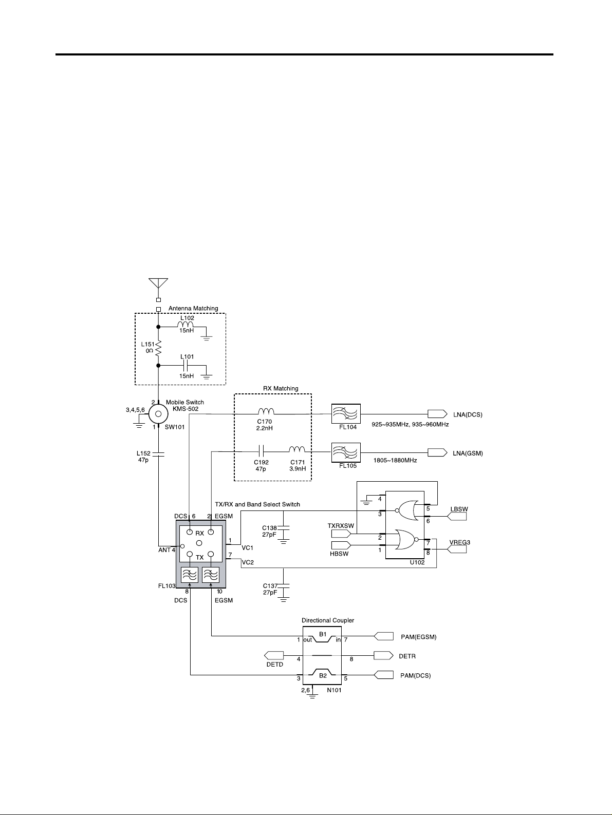
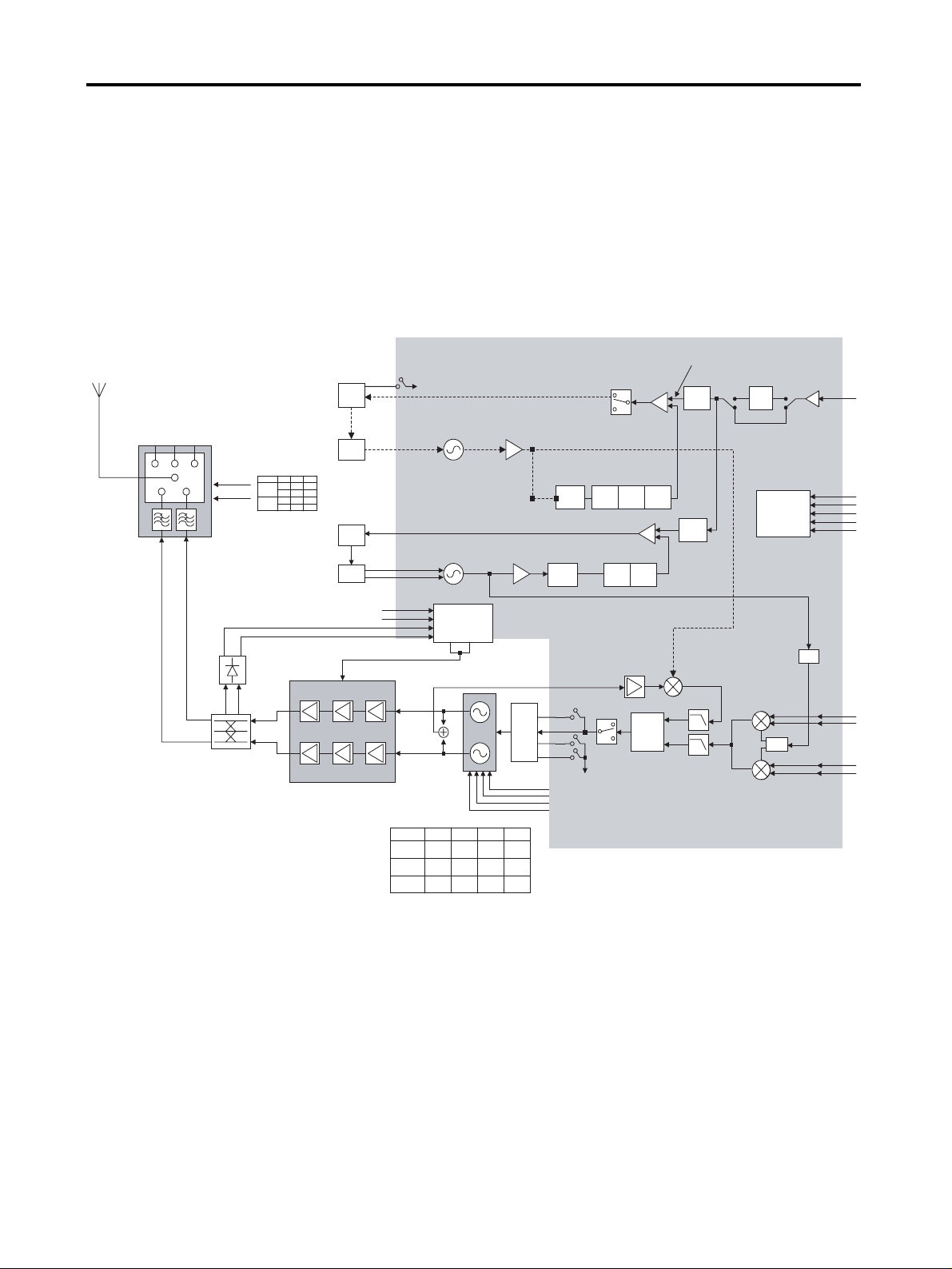
The receiver part consists of a dual band (GSM & DCS) antenna switch, two RF SAW filters, an
external dual RF VCO and a transceiver IC (TRF6150). All active circuits for a complete receiver
chain with the exception of RF VCO are contained in the transceiver IC (TRF6150).
The TRF6150 chip set has direct conversion structure, so the received RF signal is directly
converted to base band I and Q signal by the transceiver IC (IF frequency is 0 Hz), which contains
two LNAs and three direct conversion demodulators for E-GSM, DCS and PCS. The demodulated I
and Q signals pass two base band AGC amplifiers and a channel filter, which are on both I and Q
signal paths. The RF front-end circuit is shown Figure 3-1.
Figure 3-1. RF front-end circuit
3. TECHNICAL BRIEF
- 12 -

3. TECHNICAL BRIEF
- 13 -
3.1.1 RF front end
RF front end consists of an antenna, a dual band antenna switch, two RF SAWs and two LNAs for EGSM, DCS band, which are contained in the transceiver IC (TRF6150).
The RF received signals (GSM 925MHz ~ 960MHz, DCS 1805MHz ~ 1880MHz) are input via the
antenna or coaxial connector. An antenna matching circuit is between the antenna and the
connector.
The antenna switch (FL103) is used to control the Rx and TX paths, which has two control signals
VC1 and VC2 that are connected to 4-Input NOR Gate (U102) to switch either TX or RX path on.
When the RX path is turned on, the received RF signal, which has passed through the dual band
antenna switch, is filtered by an appropriate RF SAW filter for better stop band rejection. The filtered
RF signal is amplified by an LNA integrated in the transceiver IC(TRF6150) and pass to a direct
conversion demodulator. This process is the same both GSM and DCS.
The logic and current is given below. Table 3-1.
Table 3-1. The logic and current
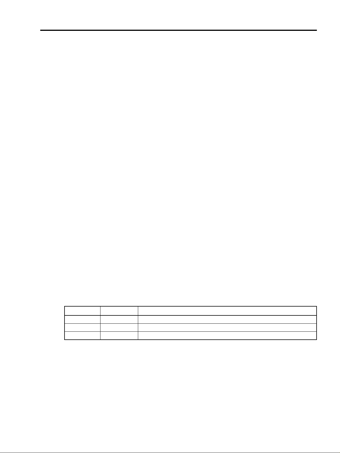
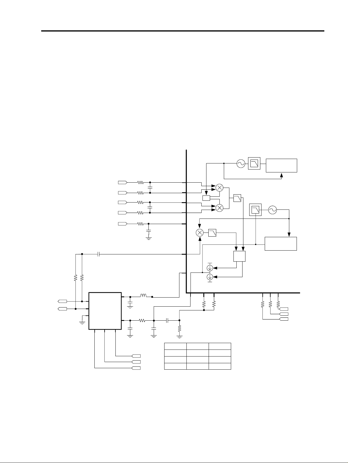
3.1.2 Demodulator and Baseband Processing
IF stage is not necessary in this system because the receiver is based on direct conversion
architecture. So the RX LO frequency is the same as input radio frequency. The amplified signal at
LNA stage passes to a direct conversion demodulator and is mixed down to generate I&Q BB
signals. The BB I&Q signals pass via two integrated baseband amplifiers with digitally programmable
gain and two fully integrated baseband channel filters to the baseband A/D converters which is
contained in baseband chipset. Figure 3-2 shows RX path block diagram.
3.1.3 DC offset compensation
The transceiver IC(TRF6150) is based on direct-conversion architecture. This implies that a parasitic
DC offset may appear at the output of the IQ demodulator. To reduce the static offset due to
components mismatch and LO self-mixing, the IC includes a hardware DC offset compensation
circuit on both I and Q base band paths. The transceiver IC uses a divider by 2 for LO generation in
EGSM and a multiplier by 2 in DCS to minimize the DC offset generated by self mixing and the LO
radiation. In addition, a quadrature demodulator gain mismatch calibration system is used to reduce
the signal distortion.
VC1 VC2
GSM TX 2.7 V 0 V
DCS TX 0 V 2.7 V
GSM/DCS RX 0 V 0 V

Figure 3-2. RX path block diagram
Table 3-2. Gain and Noise Figure of RX path
Table 3-3. Total Gain and Noise Figure of RX path
3. TECHNICAL BRIEF
- 14 -
Ant. switch RF SAW Filter I,Q demodulator (LNA+Mixer)
Gain(dB)
GSM -0.6 -2.5 26
DCS -0.7 -2.4 23
NF(dB)
GSM 3
DCS 3.5
Total Gain Total Noise Figure
GSM, EGSM 22.9 dB 7.2 dB
DCS 19.9 dB 7.4 dB
3. TECHNICAL BRIEF
- 15 -
3.2 Synthesizer
The TRF6150 includes two synthesizer parts. Two synthesizers consist of an IF synthesizer, which is
an integer-N synthesizer, and a RF synthesizer, which is a fractional-N synthesizer. The TRF6150 is
a transceiver IC suitable for GSM and DCS GPRS up to class 12 applications. So, synthesizers use
a number of techniques to improve lock time, making them well suited to GPRS.
The main fractional-N synthesizer (RF synthesizer), which includes a RF VCO with external tank
circuits, is necessary for both transmitting and receiving operation. The RF VCO works only when
the transmitting operation is on. The main fractional-N synthesizer has frequency band from 1294
MHz to 1356 MHz. Output frequency of the RF VCO is set by the factional number, prescaler and
counter. A buffer amplifier follows the RF VCO. The purpose of the buffer is to give reverse isolation
and prevent any frequency pulling of the VCO when the transceiver is powered UP and DOWN.
A dual band external VCO, which uses the PLL block of the main fractional-N synthesizer, is
necessary for transmitting and receiving operation. The dual band means that it can support GSM,
DCS frequency operation. For transmitting operation, the OPLL block of the TRF6150 directly
modulates the dual band external VCO with I and Q signals. For receiving operation, the external
VCO output frequency band is from 902 to 940MHz for DCS Rx and from 1850 to 1920MHz for GSM
Rx. The frequency of the signal from the external VCO is divided by 2 for GSM Rx and is doubled by
2 for DCS Rx operation before entering into the direct conversion mixer.
The auxiliary integer-N synthesizer (IF synthesizer), which includes an IF VCO with external tank
circuits, is necessary for transmitting operation only. The IF VCO has a frequency band from 832
MHz to 858 MHz. Output frequency of IF VCO is settled by prescaler and counter. The fractional
counter in the RF synthesizer just differs from the IF synthesizer. The IF VCO is also followed by a
buffer amplifier, which is to give reverse isolation and prevent any frequency pulling of the VCO
when the transceiver is powered UP and DOWN.
A fixed reference frequency of 1.3MHz for Rx (or 2.6MHz for Tx) is generated by a reference divider
from the external applied 13 MHz crystal oscillator.
The phase frequency detector with charge pump provides programmable output current, which could
drive the capability and the pulse width.
The counter and mode settings of the synthesizer in the TRF6150 are programmed via 3-wire
interface.
Table 3-4. 3-wire BUS of Synthesizer in the TRF6150
Pin Number Description
TSPCLK 11 Serial clock input to the synthesizer
TSPDATA 12 Serial data input to the synthesizer
TSPEN 13 Input latches the serial data transferred to the synthesizer
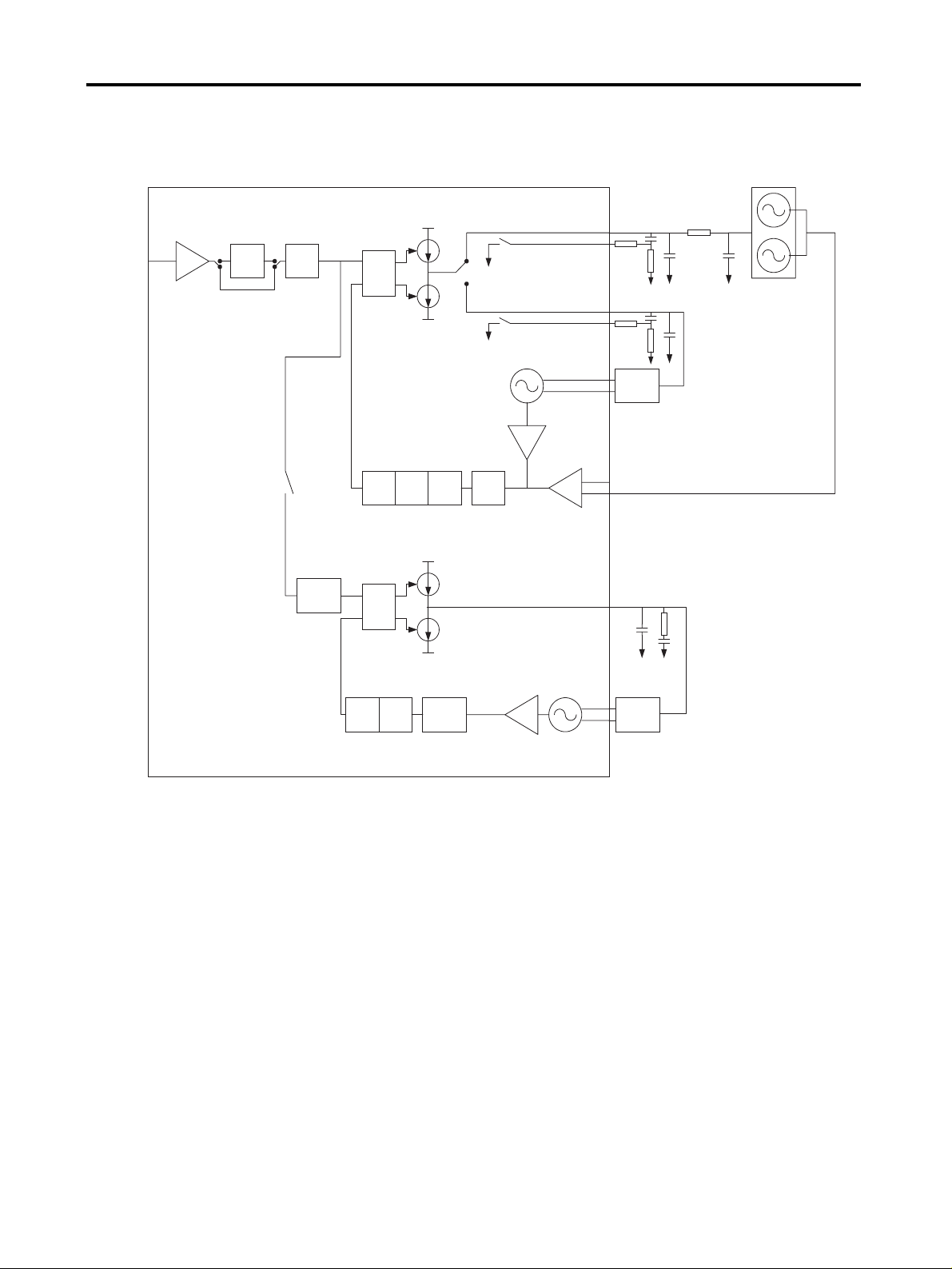
Figure 3-3. Synthesizer internal Block Diagram
3. TECHNICAL BRIEF
- 16 -
PFD
6 bitsA3bits
B
8/9
P/P+1
Delay
16/17
P/P+1
7 bitsA4 bitsB4 bits
FN
: 5/ 10
PFD
: 2
TANK
TANK
832 ~ 858MHz
IF SYNTHESIZER
2.6MHz
RX : OPEN
TX : CLOSED
RF SYNTHESIZER
2.6/1.3MHz
1294 ~ 1356MHz
Dual band VCO :
902 ~ 940MHz DCS Rx
1850 ~ 1920MHz GSM Rx
13MHz
or
26MHz
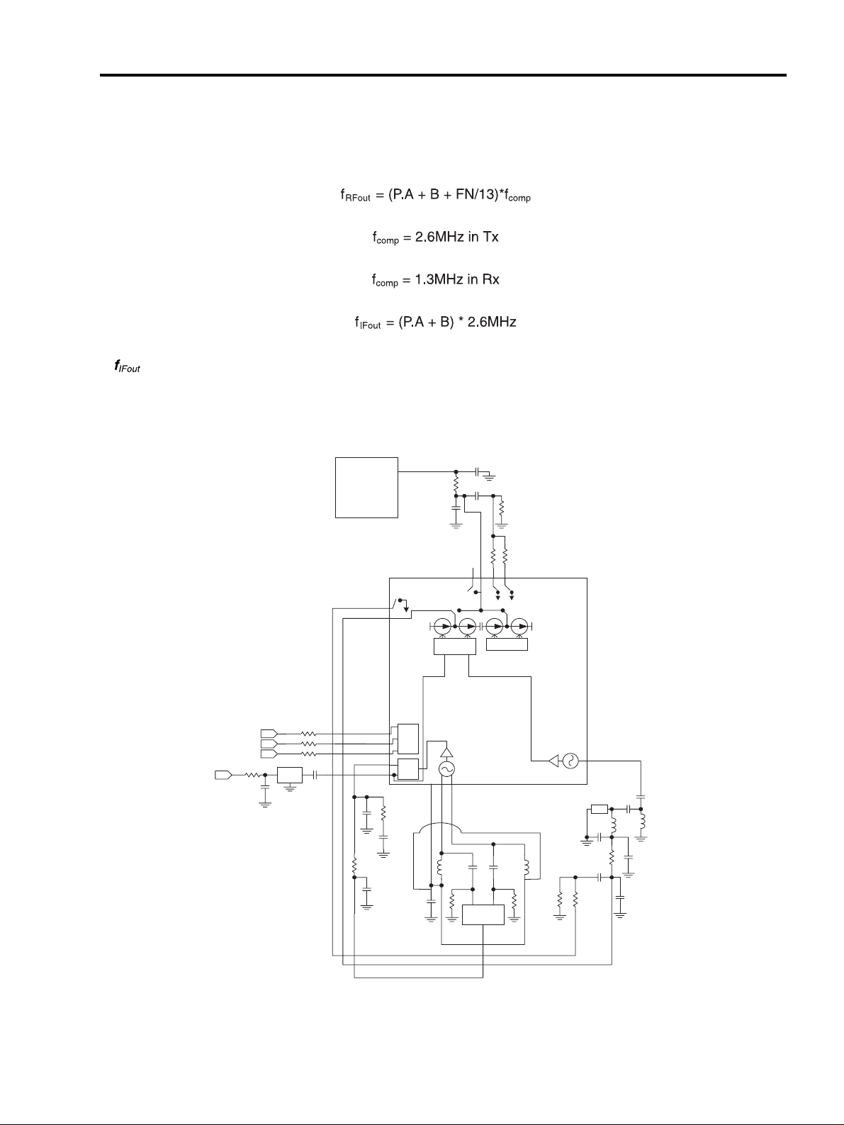
The IF and RF output frequencies of the TRF6150 are set by programming the internal divider registers.
The frequency setting equations of the IF and RF frequencies are as follows.
is the output frequency of the IF VCO (the auxiliary integer-N synthesizer) and fRFout is the output
frequency of the RF VCO (the main fractional-N synthesizer). The frequency band of the RF VCO is from
1294MHz to 1356 MHz, and the frequency band of the IF VCO is from 832MHz to 858Mhz, which
frequency bands are only for the transmitting operation.
Figure 3-4. Synthesizer circuit
3. TECHNICAL BRIEF
- 17 -
U105
TRF 6150
CLK 11
DATA 12
EN 13
AUXCP 14
CRF 16
MAINSPUP14
MAINCP 5
VCC7 22
AUXVCOP 23
AUXVCON 24
35 MAINVCO
59
TXRXCP
58 R2
57 MAINSPUP2
AFC
R131
C142
X101
VC-TCXO-208C
C146
R128
R123
R124
TSPEN
TSPDATA
TSPCLK
C175
R140
C174
R141
C178
L109
C179
R142
C176 C177
R143
L110
D103
R139
R137
C184
C183
C185
R145
C167
L105
C164
L108
C156
R109
R110
R111
C118
C117
R107
C116
VT 13
FL101
ENFVF382S18
D102
HVC369B
AUX.
PLL
Serial
Interface
MAIN
PLL
PFD
60
SMV 1233-074
3.3 Transmitter
The Transmitter part contains TRF6150 active parts, PAM, coupler, dual schottky diode and dual
band VCO. The TRF6150 active parts consist of the vector modulator and offset phase-locked loop
block (OPLL) including down-converter, phase detector, and APC IC for power control. The VCO
feed the output frequencies into PAM and TRF6150 for Tx local frequency. The peak output power
of the PAM is controlled by means of a closed feedback loop. A dual band directional coupler is
used to control the RF output from the PAM. The PAM outputs from the directional coupler pass to
the antenna connector via an integrated dual band antenna switch module.
Figure 3-5.Transmitter Block Diagram
3. TECHNICAL BRIEF
- 18 -
CLARA
TRF6150
LF PFD
PF08122B
IN
IP
QN
QP
HBRX
LBTX
HBTX
TXRXcp
OMIXrf
HBswitch
LBswitch
TXRXswitch
Vreg3
CRF
LF
:5/10 :2
7bits
A
4bits
B
6bits
A
3bits
B
8/9
P/P+1
LF
TANK
TANK
16/17
P/P+1
4bits
FN
Vapc FILT
DETD
DETR
APC DAC
APCEN
AUXcp
AUXvcop
AUXvcon
MAINcp
Delay
PA
CONTROLLER
Serial Control
Logic &
Resisters
VR4in
CLK
EN
DATA
90˚
/2
MAINvco
R3
MAINspup2
R 2
MAINspup1
LDC15D190A0007A
BAT15-05W
VC1
VC2
SHS-M090B
ENFVF382S18
EGSMDCS
L.B./L.P. L.B./H.P. H.B./L.P.H.B./H.P.
L.B
ON/OFF
H.B
ON/OFF
RX/TX
SWITCH
00
00
00
11
11
11
ON=0/OFF=1
RX=1/TX=0
VC1 VC2
TX
RX
TX
RX
GSM
DCS
2.6V
2.6V0V0V
0V 0V
0V0V
RESETZ
2.6/1.3MHZ
1294~1356 MHz
832~858 MHz
416-429MHz
IFout = (P*A + B)*13MHz
RFout_tx = (P*A + B + FN/13)*2.6MHz
RFout_rx = (P*A + B + FN/13)*1.3MHz
RFout_rx = (P*A + B + FN/13)*1.3MHzRFout_rx = (P*A + B + FN/13)*1.3MHz
RFout_rx = (P*A + B + FN/13)*1.3MHz
TX
RX
3. TECHNICAL BRIEF
- 19 -
3.3.1 Tx Modulator
The Tx I & Q signals from BB analog chipset are fed to the TRF6150 Tx modulator, where they are
modulated onto either a Tx of 880 MHz(for GSM-Tx) or 1710 MHz(for DCS-Tx) by the quadrature
mixer inside the U604. The Tx LO signal(1294 – 1356 MHz, 426.4 MHz) is fed from the internal main
and aux. VCO.
The modulator provides more than 40dBc of carrier and unwanted side-band rejection and produces
a GMSK modulated signal. The BB software is able to cancel out differential DC offsets in the I/Q BB
signals caused by imperfections in the D/A converters. The Tx-Modulator implements a quadrature
modulator. The frequency input signal is split into two precise orthogonal carriers, which are
multiplied by the BB modulation signal IP/IM and QP/QM. It is used as reference signal for the OPLL.
Figure 3-6. Tx IF Modulator and OPLL Circuit
51
59
58
62
OMIXRF
VREG3
MAINSPUP2
R2
57
TXRXCP
FL101
ENFVF382S18
R113
R114
1710 - 1785MHz(TX, DCS)
880 - 915MHz(TX, GSM)
TXVCO
LBSW
10
VT
GSM_OUT
11
13
1
VCC
C123
C110
R107
C117
C116
C118
R109
6
DCS_OUT
DCS_SW
PWR_SW
8
9
GSM_SW
HBSW
TXRXSW
GND
2,5,7 12,14
R110
R111
TRF6150
U105
11
TSPCLK
TSPDATA
TSPEN
18
QN
19
QP
22
RESETZ
QP
IP
IM
QM
RESETCL
R505
R506
C502
R501
20 IN
21
IP
R502
R129
C501
C143
DATA
1312
R124
R123
R128
CLK EN
:2
PFD
AUX PLL
N-integer
MAIN PLL
N-fractional
TXRXSW
LBSW
HBSW
GSM TX DCS TX
0 0
0 1
1 0
L153

3.3.2 OPLL
The down converter contained inside of the TRF6150 (U105) mixes the Tx RF frequency with the RF
VCO signal from the ENFVF382S18 (FL101) to generate a ‘feedback’ signal at 414.4MHz for
GSM,EGSM and DCS operation. The ‘feedback’ signal passes to one port of the phase detector.
The GMSK ‘reference’ signal from the Tx IF modulator passes via a second limiter to the other input
port of the phase detector. The phase detector generates an error current proportional to the phase
difference between the ‘feedback’ signal from the down-converter and the ‘reference’ signal from the
Tx IF modulator.
The error current is filtered by a second order low-pass filter to generate an output voltage, which
depends on the GMSK modulation and the desired channel frequency. This voltage controls the
transmit VCO such that the VCO output signal, centered on the correct RF channel is frequency
modulated with the original GMSK data. The center frequency of the transmit VCO is offset from the
RF VCO frequency by 414.4MHz for GSM, EGSM and DCS oper ation.
3.3.3 Power Amplifier
The PF08122B (U101) is Dual band power amplifier for EGSM (880 to 915 MHz) and DCS (1710 to
1785 MHz). The efficiency of module is the 55% at 35 dBm for E-GSM and the 50% at 32.5 dBm for
DCS for 3.5 V nominal battery use.
This module should be operated under the GSM burst pulse. To avoid permanent degradation, CW
operation should not be applied. To avoid the oscillation at no input power, before the input is cut off,
the control voltage Vapc should be control to less than 0.5 V. We have to improve thermal
resistance, the through holes should be layouted as many as possible on PCB under the module.
And to get good stability, all the GND terminals and the metal cap should be soldered to ground
plane of PCB.
Figure 3-7. Power Amplifier and its Control Part Circuits
3. TECHNICAL BRIEF
- 20 -
LDC15D190A0007A
N101
Directional Coupler
IN
OUT
1
GND
B1
B2
2,6
4
5
3
8
U101
PF08122B
C186
L150
C191
R135
R133
R134
PAM
+
H : GSM, L : DCS
C153
VBAT
C154
C130 C125
9,10,11,12
7
1
5
6
3
4
GSM
DCS
GND
Vapc
GSM
DCS
Vdd2
Vdd1
Bias Circuit
Vctl
2
8
C119
C150
C133
C198
U105
TRF6150
48
VAPC
C131
R116
R112
46
DETD
45
DETR
R138
R117
D101 BAT15-05w
C134
R119
R120
R103
47
FILT
8
APC9APCEN
R126
C188
R125
PA_LEVEL
PA_ON
FL103
SHS-M090B
7
C132
C107
C135
C136
C199
C120
L191
3. TECHNICAL BRIEF
- 21 -
3.3.4 PA Circuit and Control
The power amplifier control circuit ensures that the RF signal is regulated to the required limits of
operation. RF power is controlled by driving the power control pins of power amplifier and sensing.
The resultant RF output power via a directional coupler (N101). The RF sense voltage is peak
detected using an schottky diode of BAT15-05W (D101). This detected voltage is compared to the
DAC voltage in the TRF6150 to control the output power.
An internal input signal (PA_LEVEL) from CALYPSO, which is digital BB chipset (U503), is applied
to the APC IC in TRF6150 during the PA_ON mode and a directional coupler near the antenna feeds
a portion of the RF output signal back to the APC IC and peak detector converts this signal to a low
frequency feedback signal that balances the amplifier when this signal is equal to the RAMP input
signal level.
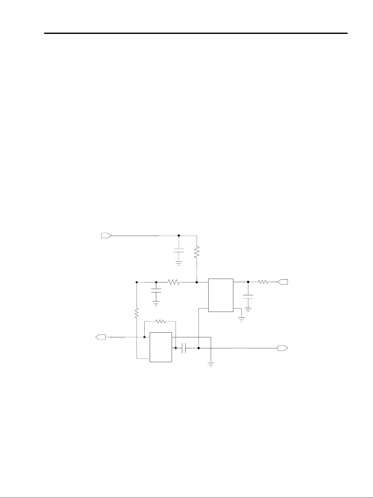
3.4 13 MHz Clock
The 13 MHz clock (VC-TCXO-208C) consists of a TCXO (Temperature Compensated Crystal
Oscillator), which oscillates at a frequency of 13 MHz.
The 13MHz clock is used within the Synthesizer block of the TRF6150, BB Analog chip-set
(NAUCICA_CS), and Digital (CALYPSO). The inverter IC, TC7SZ04AFE buffers the output to
NAUCICA_CS and CALYPSO.
Figure 3-8. VCTCXO Circuit
VC-T CXO-208C
X101
R121
R913
R130
C147
GND 2
VCONT 1
3 OUT
4 VCC
R131
C142
C140
R913
Pin#3@ U104
13MHz
CRF@TRF6150
AFC
C139
GND 3
A 2
NC 1
4 Y
5 VCC
TC7SZ04AFE
U103

3.5 Power Supplies and Control Signals
Three Regulators are integrated in the TRF6150 to provide DC power to the RF blocks (Regulator
R1, R2, R3). The Regulator R1 is used to provide DC power to the receiver, the transmitter and the
PA control loop of the TRF6150. The Regulator R2 is used to provide DC power to the DC offset
compensation circuit, the auxiliary synthesizer, the main synthesizer and VCOs. The Regulator R3
is used for the external Rx/Tx VCO, switchplexer control buffer. An external regulator is used to
provide DC power to the VCTCXO (X101).
Table 3-5. Regulator Specification
Figure 3-9. External Regulator Circuit
3. TECHNICAL BRIEF
- 22 -
Regulator Voltage Powers Enable Signal
Regulator R1, R2, R3
Receiver, Transmitter,
(These are all integrated 2.8 V 0.1 V
Synthesizers, VCOs
in the TRF6150)
LP3985IBPX_2.8V (U104) 2.85 V 0.1V VCTCXO TCXO_EN
TCXO_EN
2.85V_OUT
R132
1 VEN
BYPASS 5
2 GND
3 VOUT
U104
LP3985IBPX_2.8V
VIN 4
R182
C148
VBAT_RF
C149
RADIO_TEMP
PT101
R181
R183
3. TECHNICAL BRIEF
- 23 -
3.6 Digital Baseband (DBB) Processor
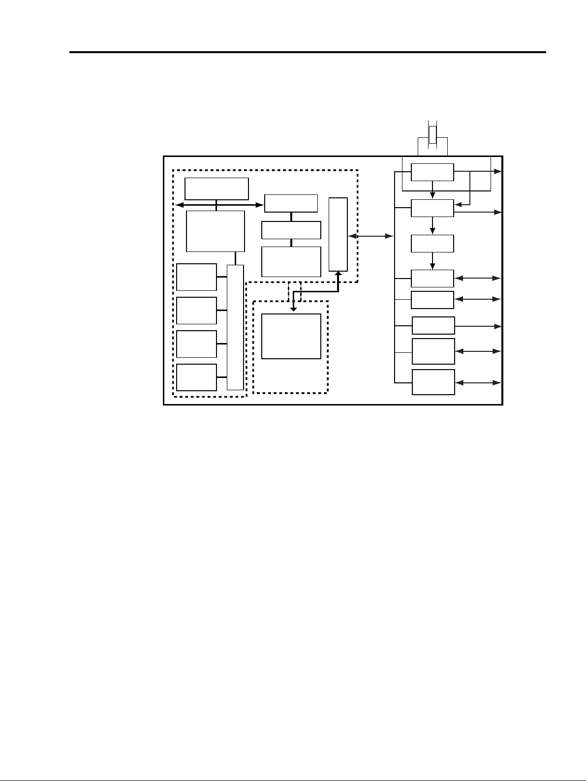
Figure 3-10. Top level block diagram of the Calypso G2 (HERCROM400G2)
3.6.1 General Description
CALYPSO is a chip implementing the digital base-band processes of a GSM/GPRS mobile phone.
This chip combines a DSP sub-chip (LEAD2 CPU) with its program and data memories, a MicroController core with emulation facilities (ARM7TDMIE), internal 8Kb of Boot ROM memory, 4M bit
SRAM memory, a clock squarer cell, several compiled single-port or 2-ports RAM and CMOS gates.
The chip will fully support the Full-Rate, Enhanced Full-Rate and Half-Rate speech coding.
CALYPSO implements all features for the structural test of the logic (full-SCAN, BIST, PMT, JTAG
boundary-SCAN).
1Mbit
SRAM
1Mbit
SRAM
1Mbit
SRAM
1Mbit
SRAM
W
r
i
t
e
b
u
f
Memory
protect
Unit
Boot ROM
External
ARM7
Memories
MEMIF
Debug Unit
ARM7
cDSP
s28c128
B
R
I
D
G
E
MCU top-cell
RREA bus
DSP subchip
8K API
GSM time
Ck32khz
IT Alarm
32KHz CRYSTAL
RTC
ULPD
TSP
TPU
SIM
PWL
UART
irda
UART
modrn

3.6.2 Block Description
CALYPSO architecture is based on two processor cores ARM7 and DSP using the generic RHEA
bus standard as interface with their associated application peripherals.
CALYPSO is composed from the following blocks:
• ARM7TDMI CPU core
• DSP subchip
• ARM peripherals:
General purpose peripherals
• ARM Memory Interface for external RAM, Flash or ROM
• 4 Mbit Static RAM with write-buffer
Application peripherals
• ARM General purposes I/O with keyboard interface and two PWM modulation signals
• UART 16C750 interface (UART_IRDA) with
- IRDA control capabilities (SIR)
- Software flow control (UART mode).
• UART 16C750 interface (UART_MODEM) with
- hardware flow protocol (DCD, CTS/RTS)
- autobaud function
• SIM Interface.
• TPU (Time Processing Unit) : Processing for GSM time base
• TSP (Time Serial Port) : GSM data interface with RF and ABB
Memory Interface : External/Internal Memory Interface
nCS0 : FLASH1, 16bit access, 3 wait state
nCS1 : Pseeudo - SRAM, 16bit access, 3 wait state
nCS2 : Not Used
nCS3 : Not Used
nCS6 : Int SRAM, 32bit access, 0 wait state
* Calypso internal 39MHz machine 3 wait state is necessary for the 80ns access because of 25ns
machine cycle. (25*4 = 100ns)
3. TECHNICAL BRIEF
- 24 -
 Loading...