


Table Of Contents
1. INTRODUCTION................................…5
1.1 Purpose ............................................….
1.2 Regulatory Information ..........................
1.3 Abbreviations .........................................
5
5
7
2. PERFORMANCE ..............................….9
2.1 H/W Feature .....................................…..
2.2 Technical Specification ..........................
9
11
3. TECHNICAL BRIEF ............................16
3.1 General Description of RF parts ......…..
3.2 Receiver Part ...................................….
3.3 Synthesizer Part …………………………
3.4 Transmitter Part ................................….
3.5 13 MHz Clock ...................................….
3.6 Power Supplies and Control Signals .….
3.7 Digital Main Processor ......................….
3.8 Analog Main Processor ......................…
3.9 Power Management IC .....................….
3.10 Memories ........................................... .
3.11 Display and Interface ......................... .
3.12 Keypad Switches and Scanning ........ .
3.13 Microphone ........................................ .
3.14 Earpiece .....................…………………
3.15 Hands-free Interface …………………..
3.16 Headset Jack Interface ...................….
3.17 Key Back-light Illumination ..............….
3.18 LCD Back-light Illumination ……………
3.19 Speaker & MIDI IC ..........................….
3.20 CAMERA IC …………………………….
16
16
19
20
23
24
25
30
36
39
40
40
42
43
43
43
46
47
48
49
4. TROUBLE SHOOTING ................… 53
4.1 RF Components .............................….
4.2 Rx Trouble ..........................................
4.3 Tx Trouble ..........................................
4.4 Power On Trouble ..........................….
4.5 Charging Trouble ...........................….
4.6 LCD Trouble .......................................
4.7 Receiver Trouble ................................
4.8 Speaker Trouble .................................
4.9 MIC Trouble ...................................….
4.10 Vibrator Trouble ...............................
4.11 Key Backlight LED Trouble ..............
4.12 Folder on/off Trouble ………………..
4.13 SIM Detect Trouble ..........................
4.14 Earphone Trouble ............................
4.15 HFK Trouble .....................................
4.16 CAMERA Trouble ……………………
53
54
63
73
76
78
80
82
84
87
89
91
93
95
100
106
5. DISASSEMBLY INSTRUCTION .... 110
5.1 Disassembly .......................................
110
6. DOWNLOAD AND
CALIBRATION ................................ 118
6.1 Download ......................................…..
6.2 Calibration .....................................…..
118
125
7. BLOCK DIAGRAM ........................... 128
-3 -

8. CIRCUIT DIAGRAM ......................... 129
8.1 MAIN .............................................…..
8.2 Memory & MMI & PMIC ..........……….
8.3 MMI …............................................….
8.4 Audio ………..................................…..
8.5 Camera ……………………..………….
8.6 RF Circuit ………………………………
129
130
131
132
133
134
9. PCB LAYOUT .................................. 135
10. ENGINEERING MODE .................. 137
13. EXPLODED VIEW &
REPLACEMENT PART LIST ...…. 149
13.1 Exploded View ...........................……
13.2 Accessory ...............................……..
13.3 Replacement Parts
< Mechanic component > ……………..
Replacement Parts
< Main component > ………………….
149
151
152
155
10.1 BB Test [MENU 1] .....................……
10.2 RF Test [MENU 2] .....................……
10.3 MF mode [MENU 3] ...................……
10.4 Trace option [MENU 4] ..............……
10.5 Call timer [MENU 5] ..................……
10.6 Fact. Reset [MENU 6] ................……
10.7 S/W version [MENU 7] ...............……
138
140
141
142
142
142
142
11. STAND ALONE TEST ................... 143
11.1 Introduction ................................……
11.2 Setting Method ..........................……
11.3 Means of Test ............................……
143
143
144
12. AUTO CALIBRATION ................... 146
12.1 Overview ....................................……
12.2 Requirements ............................……
12.3 Menu and Settings ........................…
12.4 AGC …………………………………..
12.5 APC …………………………………...
12.6 ADC ……………………………………
12.7 Setting …………………………………
12.8 How to do calibration .................……
146
146
146
148
148
148
148
148
-4 -

1. INTRODUCTION
1. INTRODUCTION
1.1 Purpose
This manual provides the information necessary to repair, calibration, description and download the
features of this model.
1.2 Regulatory Information
A. Security
Toll fraud, the unauthorized use of telecommunications system by an unauthorized part (for example,
persons other than your company’s employees, agents, subcontractors, or person working on your
company’s behalf) can result in substantial additional charges for your telecommunications services.
System users are responsible for the security of own system. There are may be risks of toll fraud
associated with your telecommunications system. System users are responsible for programming and
configuring the equipment to prevent unauthorized use. The manufacturer does not warrant that this
product is immune from the above case but will prevent unauthorized use of common-carrier
telecommunication service of facilities accessed through or connected to it.
The manufacturer will not be responsible for any charges that result from such unauthorized use.
B. Incidence of Harm
If a telephone company determines that the equipment provided to customer is faulty and possibly
causing harm or interruption in service to the telephone network, it should disconnect telephone service
until repair can be done. A telephone company may temporarily disconnect service as long as repair is
not done.
C. Changes in Service
A local telephone company may make changes in its communications facilities or procedure. If these
changes could reasonably be expected to affect the use of the this phone or compatibility with the network,
the telephone company is required to give advanced written notice to the user, allowing the user to take
appropriate steps to maintain telephone service.
D. Maintenance Limitations
Maintenance limitations on this model must be performed only by the manufacturer or its authorized agent.
The user may not make any changes and/or repairs expect as specifically noted in this manual. Therefore,
note that unauthorized alternations or repair may affect the regulatory status of the system and may void
any remaining warranty.
-5 -

1. INTRODUCTION
E. Notice of Radiated Emissions
This model complies with rules regarding radiation and radio frequency emission as defined by local
regulatory agencies. In accordance with these agencies, you may be required to provide information such as
the following to the end user.
F. Pictures
The pictures in this manual are for illustrative purposes only; your actual hardware may look slightly different.
G. Interference and Attenuation
Phone may interfere with sensitive laboratory equipment, medical equipment, etc.Interference from
unsuppressed engines or electric motors may cause problems.
H. Electrostatic Sensitive Devices
ATTENTION
Boards, which contain Electrostatic Sensitive Device (ESD), are indicated by the sign.
Following information is ESD handling:
• Service personnel should ground themselves by using a wrist strap when exchange system
boards.
• When repairs are made to a system board, they should spread the floor with anti-static mat
which is also grounded.
• Use a suitable, grounded soldering iron.
• Keep sensitive parts in these protective packages until these are used.
• When returning system boards or parts like EEPROM to the factory, use the protective
package as described.
-6 -
1.3 Abbreviations
For the purposes of this manual, following abbreviations apply:
Automatic Power ControlAPC
BasebandBB
Bit Error RatioBER
Constant Current – Constant VoltageCC-CV
Digital to Analog ConverterDAC
Digital Communication SystemDCS
1. INTRODUCTION
dB relative to 1 milli wattdBm
Digital Signal ProcessingDSP
Electrical Erasable Programmable Read-Only MemoryEEPROM
Electrostatic DischargeESD
Flexible Printed Circuit BoardFPCB
Gaussian Minimum Shift KeyingGMSK
General Purpose Interface BusGPIB
Global System for Mobile CommunicationsGSM
International Portable User IdentityIPUI
Intermediate FrequencyIF
Liquid Crystal DisplayLCD
Low Drop OutputLDO
Light Emitting DiodeLED
Offset Phase Locked LoopOPLL
-7 -
1. INTRODUCTION
Power Amplifier ModulePAM
Printed Circuit BoardPCB
Programmable Gain AmplifierPGA
Phase Locked LoopPLL
Public Switched Telephone NetworkPSTN
Radio FrequencyRF
Receiving Loudness RatingRLR
Root Mean SquareRMS
Real Time ClockRTC
Surface Acoustic WaveSAW
Subscriber Identity ModuleSIM
Sending Loudness RatingSLR
Static Random Access MemorySRAM
Pseudo SRAMPSRAM
Side Tone Masking RatingSTMR
Travel AdapterTA
Time Division DuplexTDD
Time Division Multiple AccessTDMA
Universal Asynchronous Receiver/TransmitterUART
Voltage Controlled OscillatorVCO
Voltage Control Temperature Compensated Crystal OscillatorVCTCXO
Wireless Application ProtocolWAP
-8 -
2. PERFORMANCE
2.1 H/W Features
Item Feature Comment
Standard Battery
Stand by Current
Talk time Up to 3hours (GSM TX Level 7)
Stand by time Up to 200hours (Paging Period: 9, RSSI: -85 dBm)
2. PERFORMANCE
Li-ion, 770 mAh
Size: 35 × 62 × 3.8mm
Weight: 16g
Under the minimum current consumption environment
(such as paging period 9), the level of standby current
is below 4mA.
Charging time
RX Sensitivity GSM, EGSM: -105dBm, DCS: -105dBm
TX output power
GPRS compatibility Class 10
SIM card type 3V Small
Display
Status Indicator
ANT External
EAR Phone Jack Yes
PC Synchronization Yes
Standard charge: 5hours
Rapid charge: Approx. 2.5hours
GSM, EGSM: 33dBm(Level 5),
DCS: 30dBm(Level 0)
Main LCD: 128 × 160 pixel 65K Color
Sub LCD: 96 × 64 pixel 256 Color
Hard icons. Key Pad
0 ~ 9, #, *, Up/Down Navigation Key
Confirm Key, Clear Key
Send Key, END/PWR Key
Speech coding EFR/FR/HR
Data and Fax Yes
Vibrator Yes
Loud Speaker Yes
Voice Recoding Yes
C-Mike Yes
-9 -
2. PERFORMANCE
Item Feature Comment
Receiver Yes
Travel Adapter Yes
MIDI 32 Poly
Camera VGA 640 × 320 pixel
Options Hands-free kit, CLA, Data Kit
- 10 -
2.2 Technical Specification
Item Description Specification
GSM
TX: 890 + n × 0.2 MHz
RX: 935 + n × 0.2 MHz (n=1~124)
EGSM
1 Frequency Band
TX: 890 + (n-1024) × 0.2 MHz
RX: 935 + (n-1024) × 0.2 MHz (n=975~1024)
DCS
TX: 1710 + (n-512) × 0.2 MHz
RX: 1805 + (n-512) × 0.2 MHz (n=512~885)
2. PERFORMANCE
2 Phase Error
3 Frequency Error < 0.1 ppm
4 Power Level
RMS < 5 degrees
Peak < 20 degrees
GSM, EGSM
Level Power Toler. Level Power Toler.
5 33dBm ±2dB 13 17dBm ± 3dB
6 31dBm ±3dB 14 15dBm ± 3dB
7 29dBm ±3dB 15 13dBm ± 3dB
8 27dBm ±3dB 16 11dBm ± 5dB
9 25dBm ±3dB 17 9dBm ± 5dB
10 23dBm ±3dB 18 7dBm ± 5dB
11 21dBm ±3dB 19 5dBm ± 5dB
12 19dBm ±3dB
DCS
Level Power Toler. Level Power Toler.
0 30dBm ±2dB 8 14dBm ± 3dB
1 28dBm ±3dB 9 12dBm ± 4dB
2 26dBm ±3dB 10 10dBm ± 4dB
3 24dBm ±3dB 11 8dBm ± 4dB
4 22dBm ±3dB 12 6dBm ± 4dB
5 20dBm ±3dB 13 4dBm ± 4dB
6 18dBm ±3dB 14 2dBm ± 5dB
7 16dBm ±3dB 15 0dBm ± 5dB
- 11 -
2. PERFORMANCE
Item Description Specification
GSM, EGSM
Offset from Carrier (kHz). Max. dBc
100 +0.5
200 -30
250 -33
400 -60
600~ <1,200 -60
1,200~ <1,800 -60
1,800~ <3,000 -63
3,000~ <6,000 -65
5
Output RF Spectrum
(due to modulation)
DCS
Offset from Carrier (kHz). Max. dBc
GSM, EGSM
6,000 -71
100 +0.5
200 -30
250 -33
400 -60
600~ <1,200 -60
1,200~ <1,800 -60
1,800~ <3,000 -65
3,000~ <6,000 -65
6,000 -73
Offset from Carrier (kHz). Max. dBm
Output RF Spectrum
6
(due to switching
transient)
- 12 -
400 -19
600 -21
1,200 -21
1,800 -24
Item Description Specification
DCS
Offset from Carrier (kHz). Max. dBm
Output RF Spectrum
6
7 Spurious Emissions Conduction, Emission Status
8 Bit Error Ratio
(due to switching
transient)
GSM, EGSM
BER (Class II) < 2.439% @-102 dBm
DCS
BER (Class II) < 2.439% @-100 dBm
400 -22
600 -24
1,200 -24
1,800 -27
2. PERFORMANCE
9 RX Level Report Accuracy ±3 dB
10 SLR 8±3 dB
Frequency (Hz) Max.(dB) Min.(dB)
11 Sending Response
12 RLR 2±3 dB
100 -
200 -
300 -12
1,000 -6
2,000 -6
3,000 -6
3,400 -9
4,000 -
-12
0
0
0
4
4
4
0
- 13 -
2. PERFORMANCE
Item Description Specification
Frequency (Hz) Max.(dB) Min.(dB)
13 Receiving Response
* Mean that Adopt a straight line in between 300 Hz
and 1,000 Hz to be Max. level in the range.
14 STMR 13±5 dB
15 Stability Margin > 6 dB
dB to ARL (dB) Level Ratio (dB)
100 -
200 -
300 -7
500 -5
1,000 -5
3,000 -5
3,400 -10
4,000
-35
-30
-12
0
2
*
0
2
2
2
17.5
22.5
-20
16 Distortion
17 Side Tone Distortion Three stage distortion < 10%
18
19 32.768KHz tolerance ≤ 30 ppm
20 Ringer Volume
System frequency
(13 MHz) tolerance
≤ 2.5 ppm
At least 80 dB under below conditions:
1. Ringer set as ringer.
2. Test distance set as 50 cm
-10
0
7
10
30.7
33.3
33.7
31.7
25.5
- 14 -
Item Description Specification
2. PERFORMANCE
21 Charge Current
22 Antenna Display
23 Battery Indicator
24 Low Voltage Warning
Fast Charge : < 500 mA
Slow Charge : < 60 mA
Antenna Bar Number Power
5
4
3
2
1
0
Battery Bar Number Voltage
0
1
2
3
3.62 ± 0.03V (Call)
3.5 ± 0.03V (Standby)
-85 dBm ~
-90 dBm ~ -86 dBm
-95 dBm ~ -91 dBm
-100 dBm ~ -96 dBm
-105 dBm ~ -101 dBm
~ -105 dBm
~ 3.62 V
3.62 ~ 3.73 V
3.73 ~ 3.82 V
3.82 V ~
25
26 Battery Type
27 Travel Charger
Forced shut down
Voltage
3.35 ± 0.03V
1 Li-ion Battery
Standard Voltage = 3.8 V
Battery full charge voltage = 4.2 V
Capacity: 770mAh
Switching-mode charger
Input: 100 ~ 240 V, 50/60 Hz
Output: 5.2 V, 600 mA
- 15 -
3. TECHNICAL BRIEF
3. TECHNICAL BRIEF
3.1 General Description of RF parts
The RF parts consists of a transmitter part,a receiver part,a synthesizer part,a voltage supply part,a
VCTCXO part. And the main RF Chipset CX74017[U603]is a single-chip dual-band transceiver for the
extended global system for mobile communication[E-GSM900MHz]/
Digital communication system[DCS1800MHz] voice and data transfer applications.
This device integrated a direct conversion receiver architecture, a transmitter based on a modulation loop
architecture and fractional-N synthesizer part with built in TXVCO and Local-VCO.
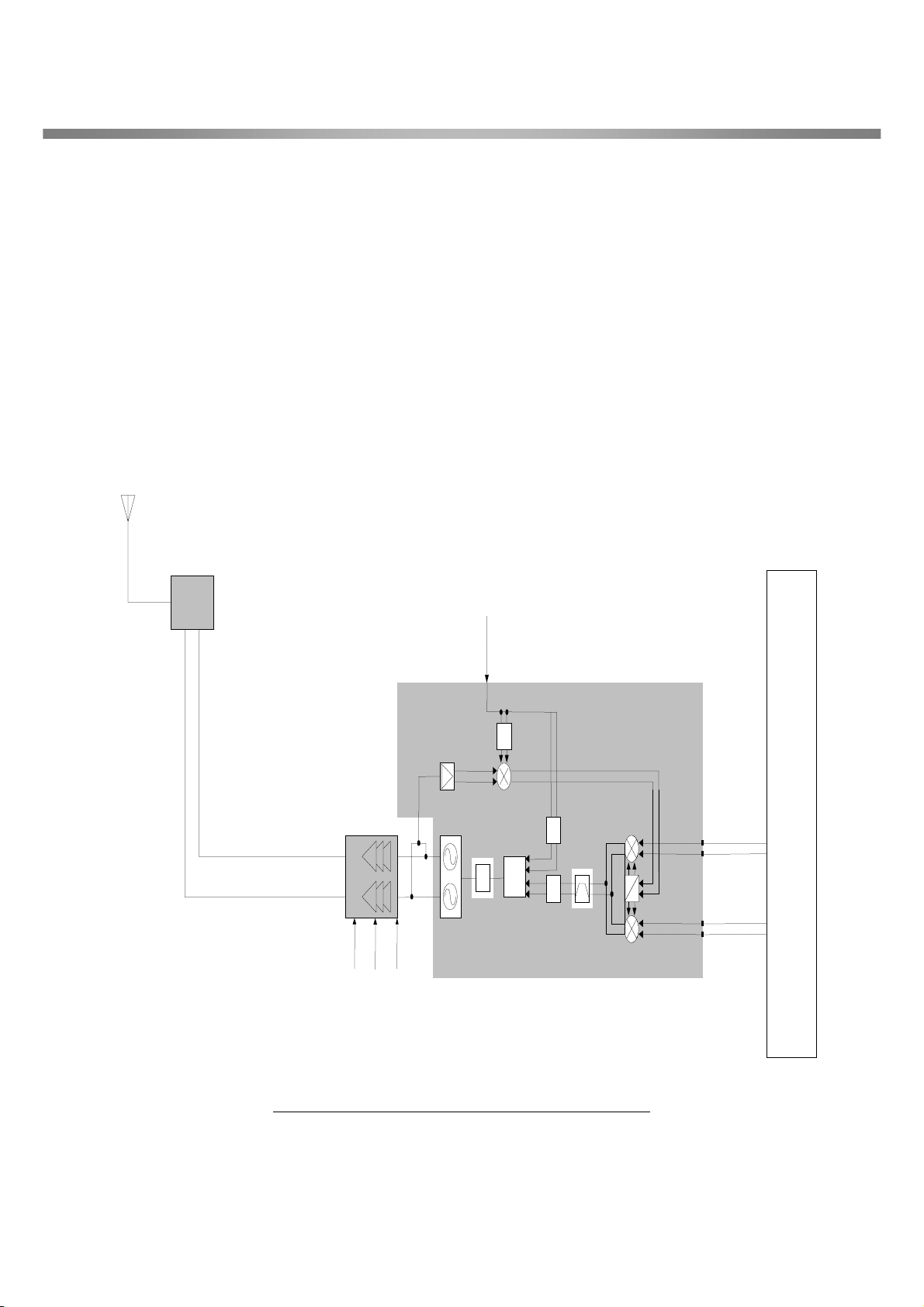
3.2 Receiver Part
The Receiver part in CX74017 contains all active circuits completely, full receiver chain with the
exception of discrete front-end RF SAW filters. The filtered and amplified signal is down converted in
the RF-mixer to the baseband output. The receiver path is supported by internal channel filtering.
DCS : 1805 ~ 1880MHz
GSM : 925 ~ 960MHz
ANT
S/W
U405(SHS-M090B)
U408(SAFSE942MAL)
U407(SAFSE1G84KA)
U603(CX74017)
0
90
VGA1 VGA2
0
90
VGA1 VGA2
DCOC
DCOC DCOC DCOC
DCOC DCOC
LO
RXQN
RXIP
RXIN
RXQP
Base
Band
Block
Figure. 3-1 Receiver Block diagram
- 16 -
3. TECHNICAL BRIEF
A. RF Front End
RF front end consists of Antenna Switch(FL405), an integrated two saw filters,(FL601),dual band
LNAs integrated in transceiver.
The Received RF signals(GSM 925MHz ~ 960MHz, DCS 1805MHz ~ 1880MHz) are fed into the
antenna or Mobile switch. An antenna matching circuit is between the antenna and the mobile
switch. The Antenna Switch(FL600) is used to control the Rx and Tx paths. And, the input signals
VC1 and VC2 of a FL600 are directly connected to baseband controller to switch either Tx or Rx
path on. Ant S/W module(FL600) is an antenna switch module for dual band phone.
The logic and current is given below table 3-1.
Table 3-1 The logic and current
CurrentVC2VC1
10.0 mA max2.5 to 3 V0 VGSM TX
10.0 mA max0 V2.5 to 3 VDCS TX
<0.1 mA0 V0 VGSM/DCS RX
The receiver part uses a low-IF receiver architecture that allows for the on-chip integration
of the channel selection filters, eliminating the external RF image reject filters and the IF
SAW filter required in conventional super-heterodyne architecture. The Receive part of
CX74017 integrates three differential input LNAs that are matched to the 200 Ohm
balanced-output SAW filters through external LC matching networks.
- 17 -

3. TECHNICAL BRIEF
B. Demodulator and baseband processing
In direct conversion receiver there is only one mixer down-converting received RF signal to BB signal
directly. The gain down converting mixer is 40dB at high gain mode and 22dB at low gain mode.
The Rx gain setting is done in the AGC algorithm. The nominal gain of the receiver is set as a
function of the expected signal strength at the antenna input so that a desired level is reached at the
Rx I/Q. 7 blocks in the receiver chain have variable gains, LNA, Mixer, LPF1, VGA1, gmC Filter,
Auxiliary gain control and VGA2. The gain settings can be adjustable via 3-wire bus control lines.
The baseband signals pass via integrated low-pass filters to the baseband A/D converters.
Theremainder of the channel filtering is performed by the baseband chipset. The demodulator
contains switches to maintain the sense of the baseband I/Q outputs with respect to the incoming RF
signal on both GSM900 and DCS1800.
C. DC offset compensation
Three correction loops ensure that DC offsets, generated in the CX74017, do not overload the
baseband chain at any point.
After compensation, the correction voltages are held on capacitors for the duration of the
receive slot(s). A rising edge on the RXEN signal, selected via the serial interface, placed the
DC compensation circuitry in the track mode.
- 18 -
3.3 Synthesizer Part
4/3 2/3
GSM
DCS
f
vco
CX74017
f
vco = (N+3.5+FN/2^22)
LF
Fractional-N
PLL
f
ref/R
/R
3. TECHNICAL BRIEF
2V7_VTCXO
13MHz
f
ref
13MHz
AFC
REFCLK
Base
Band
Block
/3
X2
DCS
GSM
The CX74017 includes a fully integrated UHF VCO with an on-chip LC tank.
A single sigma-delta fractional-N synthesizer can phase lock the local osillator used in both
transmit and receive path to a precision frequency reference input. Fractional-N operation offers
low phase noise and fast setting times, allowing for multiple slot applications such as GPRS.
The counter and mode settings of the synthesizer are also programmed via 3-wire interface.
f
LO
Figure.3-2 Synthesizer Block diagram
- 19 -
3. TECHNICAL BRIEF
3.4 Transmitter Part
The Transmitter part contains CX74017 active parts, PAM and Antenna Switch.
The CX74017 active part consists of a vector modulator and offset phase-locked loop block(OPLL)
including down-converter, phase detector, loop filter and dual band transmit VCO which can operate
at either final RF output frequency. The RF GMSK outputs from the transmit VCO are fed directly to
the RF power amplifiers. The peak output power and the profile of the transmitted burst are
controlled by means of a closed feedback loop. A dual band directional coupler is used to sample the
RF output from either PA. The PA outputs from the directional coupler pass to the antenna connector
via Antenna Switch.
FL600(LMSP54AA-097)
ANT
S/W
GSM : 880 ~ 925MHz
DCS : 1710 ~ 1785MHz
U601(CX77315))
TXRAMP TXPA
BANDSEL1
LO
f
LO
X2
f
f
TX
IF
Base
Band
TXVCO
/D1
PFD
LF
/D2
0
90
TXQP
TXQN
TXIP
TXIN
Block
Figure 3-3. RF Transmitter path Block Diagram
- 20 -

3. TECHNICAL BRIEF
A. IF Modulator
The baseband converter(BBC) within the GSM chipset generates I and Q baseband signals for the
transmit vector modulator. The modulator provides more than 40dBc of carrier and unwanted sideband rejection and produces a GMSK modulated signal. The baseband software is able to cancel out
differential DC offsets in the I/Q baseband signals caused by imperfections in the D/A converters.
The TX-Modulator implements a quadrature modulator. The IF-frequency input signal is split into two
precise orthogonal carriers, which are multiplied by the baseband modulation signal IT/ITX and
QT/QTX. It is used as reference signal for the OPLL.
B. OPLL
The offset mixer down converts the feedback Tx RF signal using LO to generate a IF modulating
signal. The IF signal goes via external passive bandpass filter to one port of the phase detector.
The other side of the phase detector input is LO signal. The phase detector generates an error
current proportional to the phase difference between the modulated signal from the offset mixer
and the reference signal from the LO. The error current is filtered by a second order low-pass filter
to generate an output voltage which depends on the GMSK modulation and the desired channel
frequency. This voltage controls the transmit VCO such that the VCO output signal, centered on
the correct RF channel, is frequency modulated with the original GMSK data. The OPLL acts as a
tracking narrowband band pass filter tuned to the desired channel frequency. This reduces the
wideband noise floor of the modulation and up-conversion process and provides significant
filtering of spurious products.
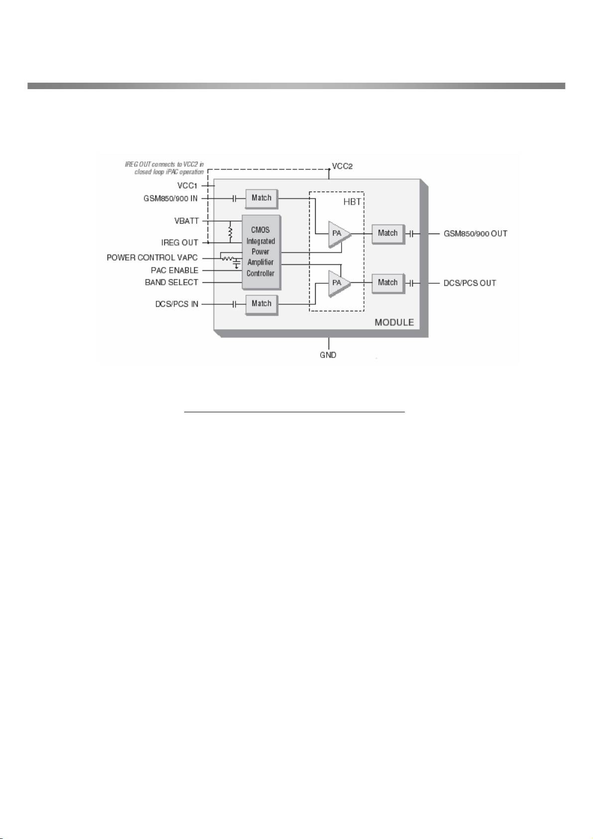
C. Power amplifier
The CX77315[U601] is designed in a compact form factor for quad-band cellular handsets comprising
GSM850/900, DCS1800, and PCS1900 operation. The PAM also supports Class 12 General Packet
Radio Service(GPRS) multi-slot operation. The module consists of separate GSM850/900 PA and
DCS1800/PCS1900 PA blocks, impedance-matching circuitry for 50 ohm input and output
impedances, and a Power Amplifier Control (PAC) block with and internal current-sense resistor.
- 21 -
3. TECHNICAL BRIEF
Figure 3-4. Power Amplifier Block Diagram
- 22 -
3. TECHNICAL BRIEF
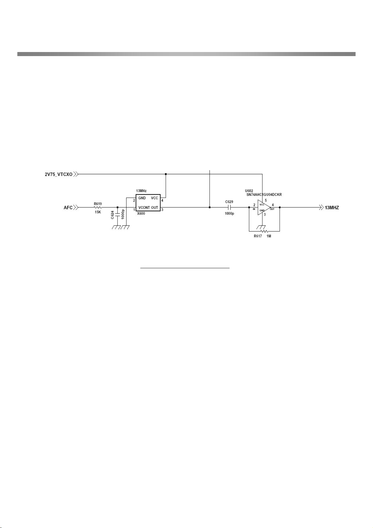
3.5 13 MHz Clock
The 13 MHz clock(X600) consists of a TCXO(Temperature Compensated Crystal Oscillator)
which oscillates at a frequency of 13 MHz. It is used within the CX74017 RF Main Chip,BB
Analog chip-set(U100 AD6521), Digital(U101 AD6525), CAMERA IC(U501 CLC344E) and
MIDI(U200) Chipset.
Figure 3-5. VCTCXO Circuit
- 23 -
3. TECHNICAL BRIEF
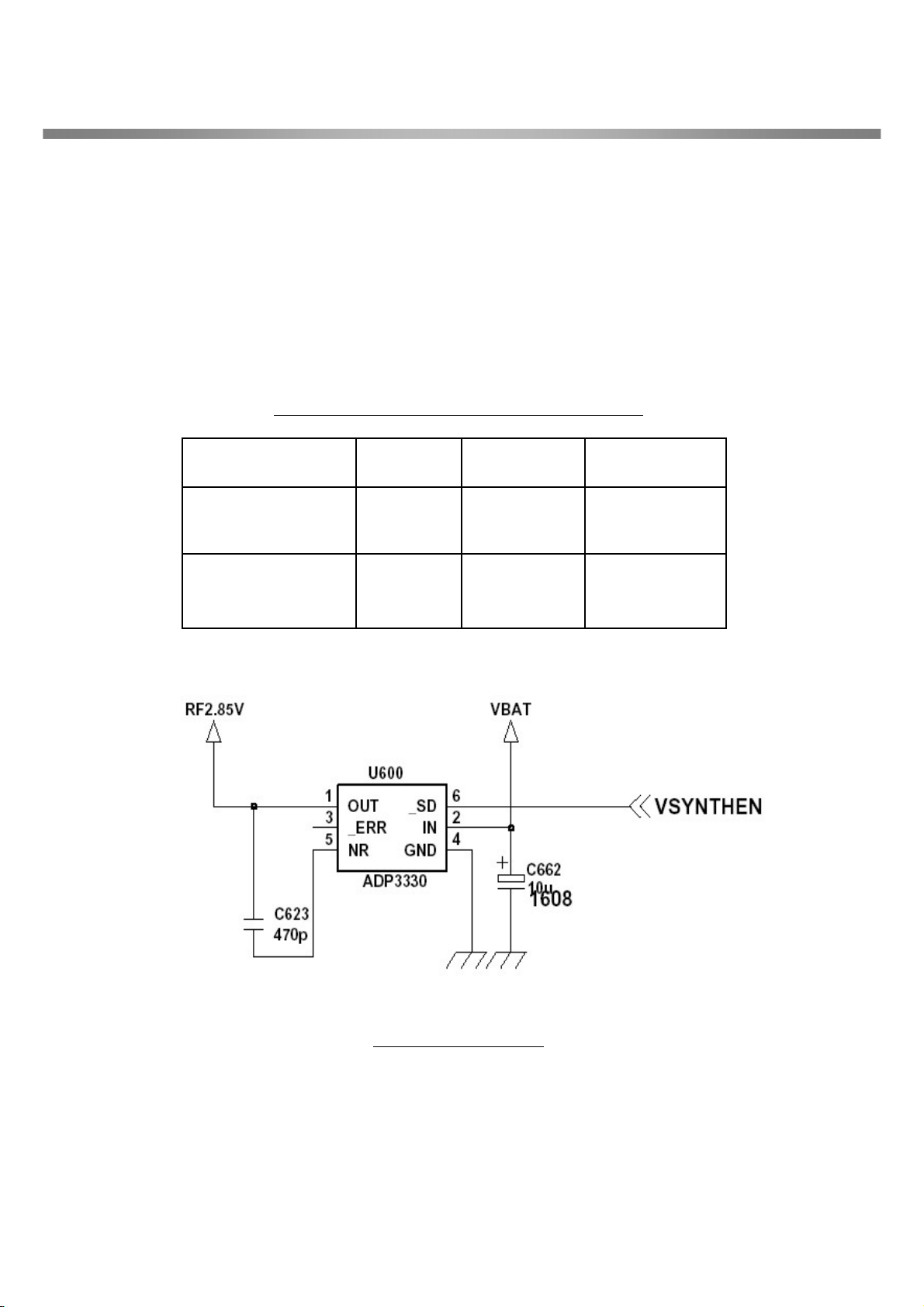
3.6 Power Supplies and Control Signals
There are two regulators used in the phone to provide RF power. One is contained inside of
ADP3522(U203), Power management IC to provide the power for the VCTCXO(X600). The other is
used to provide the power for remaining RF circuits. Figure 3-6 shows regulator 2.
Table 3-2.Power supplies and control signals.
Enable SignalPowersVoltageRegulator
Regulator 1
(U203,2V75_VTCXO)
Regulator 2
(U600,RF2.85V)
12.75V+/-
0.5V
2.85V +/-
0.5V
10.0 mA maxVTCXO
VSYNTHENRF circuitry
Figure 3-6. Regulator
- 24 -
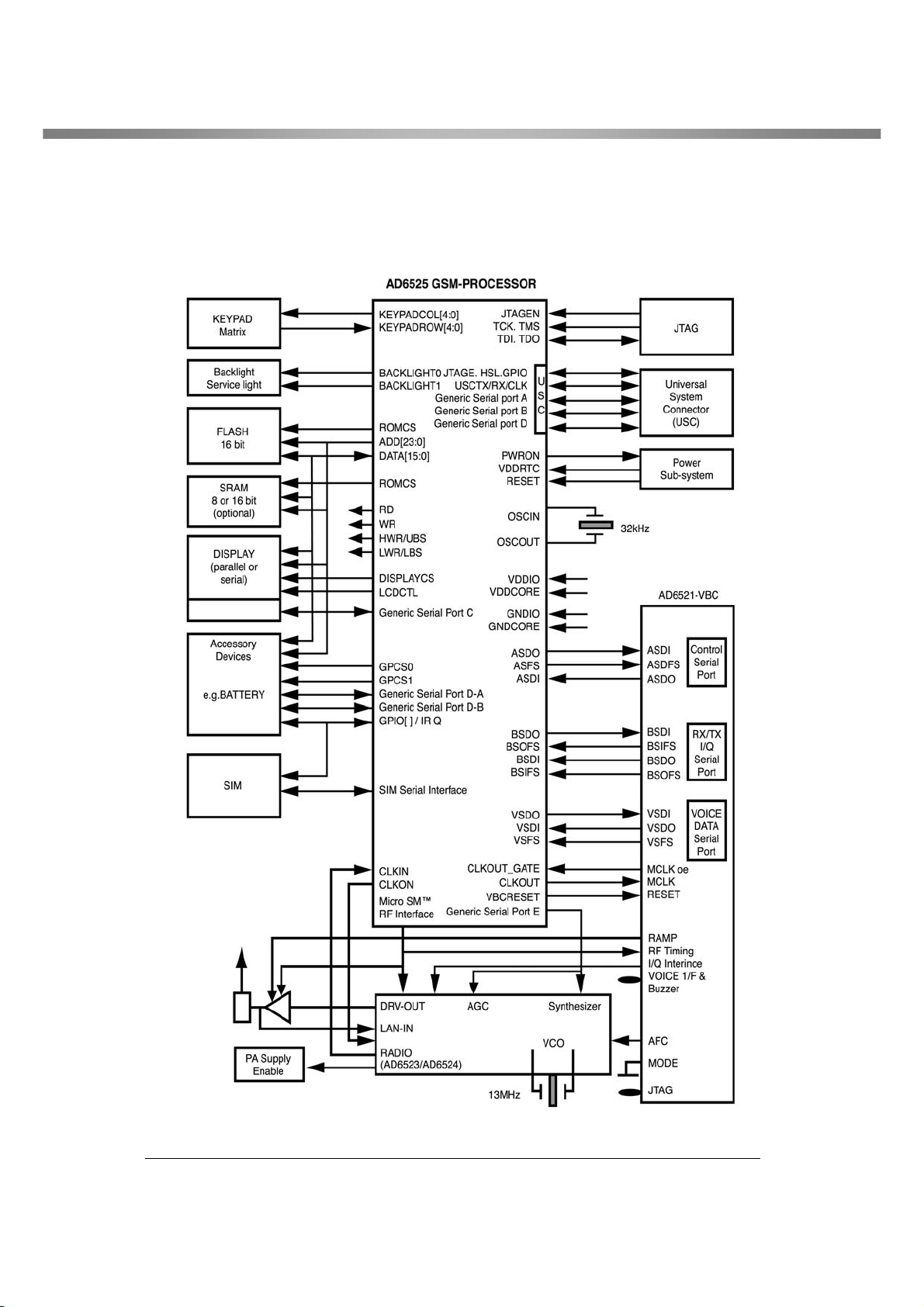
3.7 Digital Main Processor
AD6525
3. TECHNICAL BRIEF
Figure 3-7. Example of System interconnection of AD6525 External Interface
- 25 -

3. TECHNICAL BRIEF
• AD6525 is an ADI designed processor.
• AD6522 consists of
1. BUS arbitration Subsystem
• EBUS, RBUS, PBUS, SBUS, DMABUS,
IOBUS
2. DSP Subsystem
• ADI DSP, Viterbi coprocessor,
Ciphering unit,
Cache memory/controller system
3. MCU Subsystem
• ARM7TDMI, boot ROM, Clock generation and access control module
4. Peripheral Subsystem
• MMI group
⇒ Keyboard, Display, Backlight, RTC, GPIO interface
• House Keeping group
⇒ Watchdog Timer, Interrupt controller, General Timer
• GSM system group
• Direct Memory Access group
⇒ Between PBUS,RBUS, and EBUS
- 26 -
3. TECHNICAL BRIEF
3.7.1 Interconnection with external devices
A. RTC block interface
Countered by external X-TAL
The X-TAL oscillates 32.768KHz
B. LCD module interface
The LCD module is controlled by CAMERA IC, CLC344E.
If CLC344E is in the state of by-pass mode, the LCD control signals from AD6525 are by-passed
through CLC344E. In operating mode, the CLC344E controls the LCD module through
L_MAIN_LCD_CS, L_SUBLCD_CS, L_ADD1, L_WR, L_RD, L_DATA[00-15].
Table 3-3.
LCD_RS (L_ADD1)
Description
MAIN LCD driver chip enable. MAIN LCD driver IC has own CS pinL_MAIN_LCD_CS
This pin resets LCD module.LCD_RES
This pin determines whether the data to LCD module are display data
or control data. ADD1 can select 16 bit parallel bus. ADD1 is also used
to address flash memory.
Write control. The phone do not read data from LCD chip.L_WR
Parallel data lines. Color LCD driver chip uses the 16-bit data interface.L_ DATA
3V voltage is supplied to white colored LED driver for backlighting.2V8_VMEM
Control signal of white LED driver IC.LCD_BACKLIGHT
SUB LCD driver chip enable, Sub LCD driver IC has own CS pin.L_SUBLCD_CS
Parallel data lines, Sub LCD driver chip uses the 8-bit data in reface.L_DATA[08...15]
- 27 -
3. TECHNICAL BRIEF
C. RF interface
The AD6522 control RF parts through TX_EN, RX_EN, BAMDSEL1, DCSSEL, GSMSEL,
VSYNTHEN, TXPA, PLL_LE, PLL_DATA, PLL_CLK, PLL_PD
Table 3-4.
Transmitter Enable/DisableTX_EN2
Receiver Enable/DisableRX_EN3
PAM Band SelectBANDSEL14
Antenna switch Band Select(DCS Band)DCSSEL9
ResetDescriptionSignal NameGPO
Antenna switch Band Select(GSM Band)GSMSEL11
RF LDO Enable/DisableVSYNTHEN16
PAM Enable/DisableTXPA17
PLL Enable/DisablePLL_LE19
Serial Data to PLLPLL_DATA20
Clock to PLLPLL_CLK21
Powerdown InputPLL_PD22
D. SIM interface
The AD6525 check status periodically in call mode if SIM card is inserted or not, but the AD6525 don't
check in deep sleep mode.
Interface by SIMDATAOP, SIMCLK, SIM_RST(GPIO_23)
Table 3-5.
SIMDATAOP
Description
This pin receives and sends data to SIM card. This model support
1.8volt or 3.0 volt interface SIM card.
Clock 3.25MHz frequency.SIMCLK
Reset SIM blockSIM_RST(GPIO_23)
- 28 -
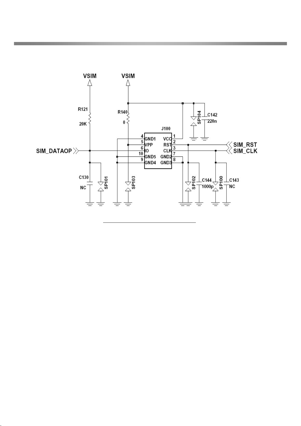
3. TECHNICAL BRIEF
Figure 3-8. SIM Interface of AD6525
E. Key interface
Include 5 column and 5 row. The AD6522 detect key press by interrupt.
F. ADP3522 interrupt
There are two interrupts, EOC and CHRDET
EOC: End of Charge. AD6525 makes charging operation stop when high signal is inputted.
CHRDET: This pin is activated when the charger is inserted.
- 29 -
3. TECHNICAL BRIEF
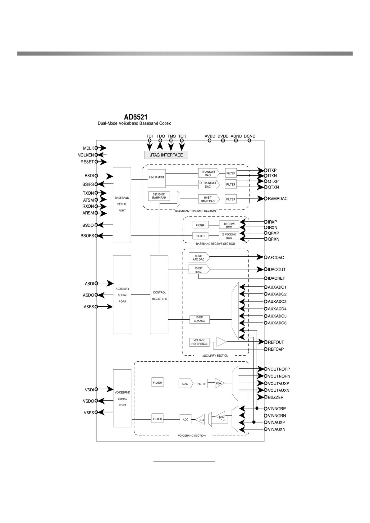
3.8 Analog Main Processor
AD6521
Figure 3-9. AD6521
- 30 -

• AD6521 is an ADI designed processor.
• AD6521 consists of
1. BB Transmit section
• This section generates in-phase and quadrature BB modulated GMSK signals.
• Digital GMSK modulator, 10-bit DACs,
Reconstruction Filter
2. BB Receive section
• 2 identical ADC channels that process BB in-phase and quadrature input signals.
3. Auxiliary section
• 2 auxiliary DASs ⇒AFC DAC, IDAC
AUX ADC
• AUX ADC : 6 channels 10 bits
AFC DAC : 13 bits
10 bits
3. TECHNICAL BRIEF
4. Voiceband section
• Receive audio signal from MIC.
Send audio signal to Speaker
• It interconnect with external device like main microphone, main receiver, earmicrophone and Hands-free kit.
- 31 -

3. TECHNICAL BRIEF
A. BB Transmit section
This section generates in-phase and quadrature BB modulated GMSK signals (BT = 0.3) in
accordance with GSM 05.05 Phase 2 specifications.
The transmit channel consists of a digital GMSK modulator, a matched pair of 10-bit DACs and a
matched pair of reconstruction filter.
B. BB Receive section
This section consists of two identical ADC channels that process baseband in-phase(I) and
quadrature(Q) input signals.
Each channel consists of a coarse switched capacitor input filter, followed by a high-order sigmadelta modulator and a lowpass digital filter.
C. Auxiliary section
This section contains two auxiliary DACs(AFC DAC, IDAC) for system control.
This section also contains AUX ADC and Voltage Reference
AUX ADC : 6 channel 10 bits
AFC DAC : 13 bits
IDAC : 10 bits
D. Voiceband section
Receive audio signal from MIC. The phones use differential configuration.
Send audio signal to Receiver. The phones use differential configuration.
It interconnects external devices such as main microphone, main receiver, ear-phone and Hands
free kit through the VINNORP, VINNORN, VOUTNORP, VOUTNORN, VINAUXP, VINAUXN,
VOUTAUXP, VOUTAUXN
VINNORP, VINNORN: Main MIC positive/negative terminal.
VOUTNORP, VOUTNORN: Main Receiver positive/negative terminal.
VINAUXP, VINAUXN: Hands free kit microphone positive/negative terminal.
VOUTAUXP, VOUTAUXON: Hands free kit speaker positive/negative terminal.
- 32 -

3. TECHNICAL BRIEF
Figure 3-10a. Voice band circuit Diagram
- 33 -

3. TECHNICAL BRIEF
Figure 3-10b. Voice band circuit Diagram
- 34 -

3. TECHNICAL BRIEF
- 35 -
Figure 3-10c. Voice band circuit Diagram

3. TECHNICAL BRIEF
3.9 Power Management IC
Figure 3-11. ADP3522 inner block diagram
Table 3-6
Description
2.85V(is provided to SIM card)VSIM
1.8V(is provided to the AD6525 & AD6521’s digital core)VCORE
2.0V(is provided to the RTC and Backup Battery)VRTC
2.55V(is provided to the AD6521 I/O and used as microphone bias)VAN
2.75V(is provided to VCTCXO)VTCXO
2.8V(is provided to Flash)VMEM
- 36 -

3. TECHNICAL BRIEF
A. Power up sequence logic
The ADP3522 controls power on sequence.
B. Power on sequence
If a battery is inserted, the battery powers the 6 LDOs. Then if PWRONKEY is detected,
the LDOs output turn on.
REFOUT is also enabled, Reset is generated and send to the AD6525.
C. LDO block
There are 6 LDOs in the ADP3522.
D. Battery charging block
It can be used to charge Lithium Ion and/or Nickel Metal Hydride batteries. The phones use
Li-Ion battery only. Charger initialization, trickle charging, and Li-Ion charging control are implemented in
hardware.
E. Charging Process
1. Check charger is inserted or not.
2. If ADP3522 detects that Charger is inserted, the CC-CV charging starts.
3. Exception: When battery voltage is lower than 3.2V, the precharge (low current charge mode)
starts firstly.
4. And the battery voltage reach to 3.2V the CC-CV charging starts.
F. Pins used for charging
CHGDET : Interrupt to AD6525 when charger is plugged.
CHGEN : Control signal from AD6525 to charge Li+ battery.
EOC : Interrupt to AD6525 when battery is fully charged.
GATEIN : Control signal from AD6525 to charge NiMH battery. But, not used.
MVBAT : Battery voltage divider. Divide ratio is 1:2.3 and it is sensed in AD6521 AUX_ADC4.
- 37 -

3. TECHNICAL BRIEF
G. TA (Travel Adaptor)
Input voltage : AC 85V ~ 264V, 47~63Hz
Output voltage : DC 5.2V(±0.2 V)
Output current : Max 750mA(±50mA )
H. Battery
Li-ion battery : Max 4.2V, Nom 4.0V
Standard battery : Capacity - 740mAh, Li-ion
- 38 -

3.10 Memories
3. TECHNICAL BRIEF
Figure 3-12. Memory block Diagram
• 128Mbit flash memory + 32Mbit PSRAM
• 16 bit parallel data bus
• ADD01 ~ ADD22.
• 2 Chip enables for Flash memory select.
• RF Calibration data, Audio parameters and battery calibration data etc are stored in Flash memory
area.
- 39 -

3. TECHNICAL BRIEF
3.11 Display and Interface
Table 3-7
144 X RGB X 177 dotsMain LCD Display Format
White LED BacklightMain LCD Backlight
96 X 64 dotsSub LCD Display Format
Sub LCD Backlight
G7100 Main LCD supports one 65536 color LCD module.
There are the control signals :
L_MAIN_LCD_CS (which is derived from CLC344E, this acts as the chip select enable for the LCD),
L_WR, L_ADD1(LCD_RS) and LCD_RES. CLC344E uses L_DATA[00:15] pins to send data for
displaying graphical text onto the LCD.
G7100 Sub LCD supports one 256 color LCD module.
There are the control signals : L_SUBLCD_CS (which is derived from CLC344E, this acts as the chip
select enable for the LCD), L_WR, L_ADD1(LCD_RS) and LCD_RES. CLC344E uses L_DATA[08:15]
pins to send data for displaying graphical text onto the LCD.
-
3.12 Keypad Switches and Scanning
The key switches are metal domes, which make contact between two concentric pads on the keypad
layer of the PCB when pressed. There are 25 switches (SW300-SW302,KB300,KB321), connected
in a matrix of 5 rows by 5 columns, as shown in Figure, except for the power switch (KD110), which
is connected independently. Functions, the row and column lines of the keypad are connected to
ports of AD6525. The columns are outputs, while the rows are inputs and have pull-up resistors built
in.
When a key is pressed, the corresponding row and column are connected together, causing the row
input to go low and generate an interrupt. The columns/rows are then scanned by AD65225 to
identify the pressed key.
- 40 -

3. TECHNICAL BRIEF
Figure 3-13. Keypad Switches and Scanning
- 41 -

3. TECHNICAL BRIEF
3.13 Microphone
The microphone is placed to the front cover and contacted to main PCB. The audio signal is passed to
VINNORP (#J10) and VINNORN (#K10) pins of AD6525. The voltage supply 2V55_VAN is output
from ADP3522, and is a bias voltage for the VINNORP. The VINNOR or VINAUX signal is then A/D
converted by the Voiceband ADC part of AD6521. The digitized speech is then passed to the DSP
section of AD6525 for processing (coding, interleaving etc.). AD6525 enables the MIC by USC3 signal,
which minimize the standby current.
VINNORP
VINNORN
Figure 3-14. Microphone
- 42 -

3. TECHNICAL BRIEF
3.14 Earpiece
The earpiece is driven directly from AD6521 VOUTNORP (#K8) and VOUTNORN (#K7) pins and the
gain is controlled by the PGA in an AD6521.
The earpiece is placed in the folder cover and contacted to LCD PCB.
Figure 3-15. Earpiece
3.15 Hands-free Interface
The audio out (VOUTAUXP & VOUTAUXN) to the hands-free kit consists of a pair of differential
signal from AD6521 auxiliary outputs (#K9, #K6), which are tracked down the board to carkit
connector (CN300) at the base of the handset. The DC level of the signal is supplied to the
VOUTAUX pin.
3.16 Headset Jack Interface
This phone chooses a 3-pole type ear-mic jack which has three electrodes such as Receiver +,
Mic+, and GND. This type usually supports only single-ended configuration in the audio path. But
most of phones use the common interface.
- 43 -

3. TECHNICAL BRIEF
Figure 3-16a. Hands-free & Headset Jack Interface
- 44 -

3. TECHNICAL BRIEF
- 45 -
Figure 3-16b. Hands-free & Headset Jack Interface

3. TECHNICAL BRIEF
3.17 Key Back-light Illumination
In key back-light illumination, there are 12 Blue LEDs in Main Board, which are driven by
KEY_BACKLIGHT line from AD6525.
Figure 3-17. Key Back-Light Illumination
- 46 -

3. TECHNICAL BRIEF
3.18 LCD Back-light Illumination
In LCD Back-light illumination, there is an driver in LCD Board, which is driven by LCD_backlight line
from AD6525.
The sub-LCD, organic light emitting diode (OLED), doesn’t need back-light illumination.
Figure 3-18. Main LCD Backlight Illumination
- 47 -

3. TECHNICAL BRIEF
3.19 Speaker & MIDI IC
LG-G7100 don’t use buzzer. but uses the loud speaker and Melody IC which makes the robust
joyful melody sounds.
• Melody IC control
2GPIO are assigned to control melody IC. Melody data is transferred to melody IC.
Figure 3-19. Speaker & MIDI IC
Basically, this phone have a melody IC of Oki ltd. ML2870(melody IC maker part number) is a
PCMbased hi-grade sound generator LSI for mobile phones that realize advanced game sounds. This
LSI stands in need of external amplifier. External amplifier used by mobile phones in addition to game
sounds and ringing melodies that are replayed by a sound generator. This melody IC has hi-grade
175 polyphonies based on General MIDI system level1, the standard spec for PCM sound generator.
- 48 -

3.20 CAMERA IC
3. TECHNICAL BRIEF
Figure 3-20. CLC344E block diagram
• External Clock Source Up to 27 MHz
• Internal Clock Divider 1/2, 1/3, 1/4 for Sensor Clock Output
• Support Standard SRAM Interface (6bit Address & 16bit Data) for CPU Interface
• 4Mbit Stacked SRAM
• Support LCD Signal By-pass Mode
• Fully Hardwired JPEG and Motion-JPEG Codec
• Support three General Port IO
• 8 x 8 100pin BGA Package
- 49 -

3. TECHNICAL BRIEF
The camera IC, CLC344E, is controlled through _RD, _WR, CAM_INT, CAM_HOLD, CAM_RST,
ADD[1-6], DATA[0-15] by AD6525. In by-pass mode, CLC344E bypasses all LCD control signal from
AD6525 to LCD module. In operating mode, CLC344E samples the image data from camera sensor
connected on CN501 through C_CD[0-7], C_MCLK, C_PCLK, C_HS, C_VS, C_SDA, C_SCK,
C_RST signals and controls the LCD module.
The camera power is provided by U500 ADP3330. It converts VBAT from battery to 2.85V
Table 3-8
Write control to CLC344E or LCD module._WR
Read control. The phone do not read data from LCD chip_RD
Interrupt to AD6525. It can be set to level or edge interruptCAM_INT
CAM_HOLD
This signal determines the camera operation mode. Making high,
disable all CLC344E functions.
This signal resets the CLC344ECAM_RST
Address lines.ADD[1-6]
Parallel data lines. DATA[0-15]
2.8V power supply to CLC344E2V85_CAM
Sensor Data bus C_D[0-7]
Sensor resetC_RST
Sensor input data sampling clockC_PCLK
Sensor clockC_MCLK
IIC bus data lineC_SDA
IIC bus clock lineC_SCK
Sensor power down control pinC_PWDN
- 50 -

3. TECHNICAL BRIEF
Figure 3-21a. CLC344E
- 51 -

3. TECHNICAL BRIEF
Figure 3-21b. Sensor connection
- 52 -

4. TROUBLE SHOOTING
4.1 RF Components
SW600
FL600
FL601
4. TROUBLE SHOOTING
U603
X600
U602
U601
Figure 4-1
Table 4-1. RF COMPONENTS
DescriptionReferenceDescriptionReference
Dual SAW FilterFL601RF Main ChipsetU603
VCTCXOX600Mobile S/WSW600
Inverter ICU602Ant. S/WFL600
PAMU601
- 53 -

4. TROUBLE SHOOTING
4.2 RX Trouble
Checking Flow Checking Points
START
HP8922 : Test mode (PCS band)
62 CH, 7 level setting (TCH)
62 CH, -60dBm setting (BCCH)
④
1. Check
Regulator Circuit
2. Check
VCTCXO Circuit
3. Check
Control Signal
4. Check
Ant SW &
Mobile SW
5. Check
Saw Filter
Circuit
⑤
①
②
⑥
Figure 4-2a
6. Check
RX IQ
Redownload SW, CAL
③
Figure 4-2b
- 54 -

4.2.1 Checking Regulator Circuit
4. TROUBLE SHOOTING
Test Points
U600 вывод 1
U600 вывод 6
Figure 4-3
Check Pin 1
RF 2.85V OK?
Yes
Regulator Circuit is OK
See next page to check
VCTCXO
Checking Flow
Check Pin 6
Pin 6 High?
No
Yes
Replace U600
Waveform
No
Change the board
Regulator part Circuit Diagram
Graph 4-1
- 55 -

4. TROUBLE SHOOTING
4.2.2 Checking VCTCXO Circuit
Test Points
X600 Pin 3 X600 Pin 4
Figure 4-4
Check Pin 3
Refer to graph 4-2
Check Pin 4
Refer to graph 4-2
Checking Flow
13MHz OK?
No
2.75V OK?
No
Check U203,ADP3522
Waveform
Yes
Yes
VCTCXO Circuit OK
See next page to check
ANT SW & Mobile SW
Change X600
Circuit Diagram
13MHz
2V75_VTCXO
Graph 4-2
- 56 -

4.2.3 Checking PLL Control Signal
Test Points Checking Flow
4. TROUBLE SHOOTING
PLL_CLK
PLL_LE
PLL_DATA
PLL_PD
Figure 4-5
Check PLL_PD
Check PLL_CLK,
PLL_DATA, PLL_LE
Check if there is any
major difference
* Refer or Graph 4-3
Waveform
Level is High?
Yes
Similar?
Yes
Control Signal is OK
See next page to check
ANT SW & Mobile SW
No
Download the SW
No
Download the SW
PLL_L
E
PLL_CLK
PLL_DAT
A
Graph 4-3
- 57 -

4. TROUBLE SHOOTING
4.2.4 Checking Ant SW & Mobile SW
For these 2 test case,
No call Connection is
needed
Check SW600 Pin 1,2 with
RF Cable connected
Check SW600 Pin 1,2 with
No RF Cable connected
Checking Flow
Open
Short
Yes
No
No
Changing SW600
Changing SW600
Check C608.2,C607.2
Check whether Ant SW set
as RX mode
* Refer to Table 4-2
Check RF Level of FL600
pin10 (for GSM)
pin 1 (for DCS)
For this RF level test
case, RX stand alone
mode is needed
Yes
VC1 : Low
VC2 : Low
Yes
Pin 10 : ~ -62dBm
Pin 1 : ~ -63dBm
Yes
Ant SW & Mobile SW is OK
See Next page to check
Saw Filter
No
No
Changing the
Board
Changing FL600
- 58 -

4. TROUBLE SHOOTING
Test Points Ant sw& Mobile sw part Circuit Diagram
SW600 Pin 1
L601
C608 Pin 2
C607 Pin 2
SW600 Pin 2
FL600
L604
Figure 4-6
Table 4-2. ANT SW Control Logic
VC2VC1ANT SW
10EGSM TX
01DCS TX
00EGSM,DCS RX
- 59 -

4. TROUBLE SHOOTING
4.2.5 Checking SAW Filter Circuit
Checking Flow
Check RF Level of Saw
Filter Input
For GSM : FL601.1
For DCS : FL601.3
Check RF Level of Saw
Filter Output
For GSM : FL601.7
For DCS : FL601.5
For these 2 test case,
RX Stand alone mode
is needed
Pin1 : ~ -61dBm
Pin3 : ~ -61dBm
Yes
Pin 7 : ~ -64dBm
Pin 5 : ~ -65dBm
Yes
Saw Filter is OK
See Next page to check Rx
IQ Signal
No
Check the parts are
well soldered
for GSM : L604
for DCS : L601
No
Check the parts are
well soldered
for GSM : L603
for DCS : L602
Changing L604 for GSM
Changing L601 for DCS
Soldering is
L603 for GSM
L602 for DCS
OK?
No
Changing
Yes
Changing
FL601
- 60 -

Test Points
4. TROUBLE SHOOTING
FL601 Pin 1
FL601 Pin 3
FL601 Pin 5
FL601 Pin 7
Figure 4-7
SAW filter part Circuit Diagram
- 61 -

4. TROUBLE SHOOTING
4.2.5 Checking RX IQ
Test Points Checking Flow
C658 C659
Figure 4-8
Check C658,C659.
Check if there is any Major
Difference
* Refer to graph 4-4
Waveform
ZOOM
Similar?
Yes
Redownload the
Software and calibrate
No
Replace U603
Graph 4-4
- 62 -

4.3 TX Trouble
④
⑤
4. TROUBLE SHOOTING
Test Points Checking Flow
START
HP8922 : Test mode (PCS band)
62 CH, 7 level setting (TCH)
62 CH, -60dBm setting (BCCH)
Spectrum analyzer setting
Oscilloscope setting
①
②
⑥
Figure 4-9a
1. Check
Regulator Circuit
2. Check
VCTCXO Circuit
3. Check
PLL Control Signal
4. Check
Ant SW &
Mobile SW
5. Check
PAM control
Signal
③
6. Check
TX IQ
Figure 4-9b
Redownload SW, CAL
- 63 -

4. TROUBLE SHOOTING
4.3.1 Checking Regulator Circuit
Test Points Checking Flow
U600 Pin 1
Check Pin 1
RF 2.85V OK?
Yes
Check Pin 6
No
Pin 6 High?
Yes
No
Change the board
U600 Pin 6
Figure 4-10
Regulator part Circuit Diagram
Regulator Circuit is OK
See next page to check
VCTCXO
Replace U600
Waveform
Graph 4-1
- 64 -

4.3.2 Checking VCTCXO Circuit
4. TROUBLE SHOOTING
Test Points
X600 Pin 3 X600 Pin 4
Figure 4-11
Check Pin 3
Refer to graph 4-2
Check Pin 4
Refer to graph 4-2
Checking Flow
13MHz OK?
No
2.75V OK?
No
Check U203,ADP3522
Waveform
Yes
Yes
VCTCXO Circuit OK
See next page to check
ANT SW & Mobile SW
Change X600
Circuit Diagram
13MHz
2V75_VTCXO
Graph 4-2
- 65 -

4. TROUBLE SHOOTING
4.3.3 Checking PLL Control Signal
PLL_CLK
PLL_LE
PLL_DATA
PLL_PD
Test Points
Figure 4-12
Check PLL_PD
Check PLL_CLK,
PLL_DATA, PLL_LE
Check if there is any
major difference
* Refer or Graph 4-3
Checking Flow
Level is High?
Yes
Similar?
Yes
Control Signal is OK
See next page to check
ANT SW & Mobile SW
No
Download the SW
No
Download the SW
PLL_L
E
PLL_CLK
PLL_DAT
A
Waveform
Graph 4-3
- 66 -

4.3.4 Checking Ant SW & Mobile SW
For these 2 test case,
No call Connection is
needed
Check SW600 Pin 1,2 with
RF Cable connected
Checking Flow
Open
4. TROUBLE SHOOTING
No
Changing SW600
Yes
For these 2 RF level
test cases, TX stand
alone mode is needed
Check SW600 Pin 1,2 with
No RF Cable connected
Check C608.2,C607.2
Check whether Ant SW set
as TX mode
* Refer to Graph 4-5
Check RF Level of FL600
pin 5 (for GSM)
pin 3 (for DCS)
Check RF Level of FL600
pin8
Short
Yes
Check DCSSEL &
GSMSEL
Yes
Pin 5 : ~ 33 dBm
Pin 3 : ~ 30 dBm
Yes
GSM : ~32 dBm
DCS: ~29 dBm
No
No
Changing SW600
Changing the Board
No
No
Goto 4.3.7
to check other RF level
Changing FL600
Ant SW & Mobile SW is OK
See Next page to check
PAM control signal
- 67 -
Yes

4. TROUBLE SHOOTING
Test Points
SW600 Pin 1
L601
C608 Pin 2
C607 Pin 2
SW600 Pin 2
FL600
L604
Figure 4-13
DCSSEL
GSMSEL
Graph 4-5a DCS TX mode
Waveform
DCSSEL
Low
GSMSEL
Low
Graph 4-5b GSM TX mode
- 68 -

4.3.5 Checking PAM Control Signal
Test Points Checking Flow
BANDSEL1
4. TROUBLE SHOOTING
TXRAMP
Figure 4-10
TXPA
Check TXRAMP, TXPA,
BANDSEL1.
Check if there is any major
difference
Refer to Graph 4-6
Waveform
Similar?
No
Yes
Control Signal is OK
See next page to check
TX IQ
Download the SW
BANDSEL1
TXRAMP
TXPA
Graph 4-6
- 69 -

4. TROUBLE SHOOTING
4.3.6 Checking TX IQ
Test Points Checking Flow
C660 C661
Figure 4-11
Check C660,C661.
Check if there is any major
difference
Refer to Graph 4-7
Waveform
Similar?
No
Yes
TX IQ signal is OK
See next page to check
RF TX Level
Download the SW
TXI
TXQ
Graph 4-7
- 70 -

4.3.7 Receiver and Transmitter RF Level
FAR-G6CS-1G8425-L250
4. TROUBLE SHOOTING
CX74017
LMSP54AA-097
⑧⑦
-63 dBm
DCS : 1805 ~ 1880MHz
GSM : 925 ~ 960MHz
-62 dBm
GSMSEL
ANT
DCSSEL
S/W
33 dBm30 dBm
-65 dBm
②④
①
-64 dBm
③
0
4/3
90
0
2/3
90
f
vco = (N+3.5+FN/2^22 )
f
vco
/3
X2
DCS
GSM
f
TX
X2
Fractional-N
LF
PLL
f
LO
f
IF
f
ref/R
f
ref
/R
Serial
I/O
Serial
I/O
13MHz
RXIP
RXIN
RXQP
RXQN
PLL_DATA
PLL_CLK
PLL_LE
PLL_PD
RXEN
TXEN
FEENA
BANDSEL1
BANDSEL2
2V7_VTCXO
13MHz
AFC
REFCLK
Base
Band
Block
GSM : 880 ~ 925MHz
DCS : 1710 ~ 1785MHz
PAM(PF08122B)
TXRAMP
TXPA
BANDSEL1
⑤
⑥
8 dBm
6 dBm
TXVCO
- 71 -
/D1
PFD
LF
/D2
0
90
TXIN
TXQP
TXQN
TXIP

4. TROUBLE SHOOTING
Test Points
②
①
⑥
④
③
⑦
⑧
Figure 4-12
- 72 -
⑤

4.4 Power On Trouble
SETTING : Connect PIF, and set remote switch off at PIF
Checking Flow
START
4. TROUBLE SHOOTING
Check Battery voltage
>3.35V ?
Yes
Push power-on key
and check the level change
of U203 pin 30
Yes
Check the voltage of
the following pins at U203
pin 21 = 1.8V?
Pin 25 = 2.75V?
Pin 20 = 2.8V?
Pin 3 = 2.0V?
Yes
No
No
Charge or Change Battery
Check the contact of
power-key or dome
switch
No
Replace U203
Logic level at Pin 29 of U203
= HIGH?
Yes
The phone will
power ON
No
Redownload software
- 73 -

4. TROUBLE SHOOTING
This signal should go HIGH
when the power-on procedure
is completed
Power-On Key
Signal Input
Power On part Circuit Diagram
These powers
should be
necessary to power
on
- 74 -

P25 : 2V75_VTCTO
4. TROUBLE SHOOTING
Test Points
P21 : 1V8_VCORE
P20 : 2V8_VMEM
P29 : RPWRON
P3 :2V0_VRTC
P30 : POWRKEY
Figure 4-13
- 75 -

4. TROUBLE SHOOTING
4.5 Charging Trouble
SETTING : Connect the battery and the charging adaptor(TA) to the phone
Checking Flow
START
Charging Connector(CN300)
well-soldered?
Yes
Voltage at Pin 7 of U203
= 5.2V?
Yes
Are R218,Q200,D200
well soldered?
Yes
Voltage across D200 < 0.3V?
Yes
Voltage across R218
is about 20~150mA?
Yes
No
No
The charging adaptor(TA) is out of order.
No
No
No
Resolder CN300
Change the charging adaptor
Resolder R218,Q200,D200
Replace D200
Replace R218
Voltage across Q200
< 1.0
Yes
Is the battery charged?
Yes
CHARGING WILL
OPERATE PROPERLY
- 76 -
No
No
Replace Q200
The battery may have the problem.
Change the battery and try again.

R218
4. TROUBLE SHOOTING
Test Points
D200Q200
The charging
current will
flow into this
direction.
Figure 4-14
Charging part Circuit Diagram
- 77 -

4. TROUBLE SHOOTING
4.6 LCD Trouble.
Checking Flow
START
Is the connection of LCD module
with connector on FPCB OK?
Yes
Is the connection of FPCB
with LCD connector on PCB OK?
Yes
Check the soldering of CN500 on
PCB
Yes
Check the soldering of pin1 on LCD
module
No
No
No
No
Reassemble LCD module with FPCB
connector
Reassemble FPCB with LCD connector
on PCB
Resolder CN500
Resolder Pin1
Yes
Does graphic data appear on LCD?
Yes
LCD Working !!
No
Replace LCD module or FPCB
- 78 -

Test Points
4. TROUBLE SHOOTING
Figure 4-15a
LCD Connector on PCB
PIN 1
Figure 4-15c
LCD Connector on LCD PCB
Figure 4-15b
LCD Module
Connection of
Pin1 on LCD
mudule
Connection of
CN500 on PCB
Figure 4-15d
FPCB Ass’y
- 79 -

4. TROUBLE SHOOTING
4.7 Receiver Trouble
SETTING : After initialize Agilent 8960, Test EGSM, DCS mode
Checking Flow
START
Check pin 33,
pin 35 of CN500. Are these
voltage almost 1.23V?
Yes
Check the soldering Receiver
Yes
Receiver will be work
properly
No
No
Check the soldering
CN500
Yes
Resoldering CN500
Replace the Main board.
ABB is out of order.
Replace the Receiver
- 80 -

4. TROUBLE SHOOTING
Test Points Receiver part Circuit Diagram
PIN 35,33
Figure 4-16
- 81 -

4. TROUBLE SHOOTING
4.8 Speaker Trouble
SETTING : Connect PIF to the phone, and Power on. Enter the engineering mode, and set
"Melodyon" at Buzzer of BB test menu.
Checking Flow
START
Check the
C201,C211. Are these
voltage = 2.8V?
Yes
Check the signal
level C208, C209
Yes
Check the
signal level Pin 6 and
Pin 10 at U201
Yes
No
No
No
Check the soldering
of U203
Yes
Resoldering U203
Check the
soldering C208,C209,R200,
R201, R202,R203
Yes
Resoldering C208,C209,
R200,R201, R202,R203
No
Replace the U203
Replace the U200
No
Replace the U201
Check the soldering Speaker
Yes
Speaker Working
No
Replace Speaker
- 82 -

Test Points
4. TROUBLE SHOOTING
R201
R203
U201
R202
R200
C201
U200
C208
Figure 4-17
C209
Speaker part Circuit Diagram
- 83 -

4. TROUBLE SHOOTING
4.9 MIC Trouble
SETTING : After initialize Agilent 8960, Test EGSM, DCS mode
Checking Flow
START
Check the C121
Voltage is almost
2.2V DC
Yes
Check the C147
voltage almost 1.9V,
C145 voltage a few
hundred mV
Yes
Check the R111
voltage almost 1.4V,
R112 voltage
almost 1.0V
No
No
Check the voltage at
Pin23 of U203 is
2.55V DC
Yes
Resoldering R115
Check the soldering
R113
Yes
Resoldering R113
No
No
Replace the U203
No
Replace the MIC100
Replace the Main Board
Yes
Is the voltage at Pin 3
of Q100 almost 0V DC?
Yes
MIC Working
No
Replace Q100
- 84 -

R112
R111
R113
C121
R115
4. TROUBLE SHOOTING
Test Points
C145
C147
Figure 4-18
- 85 -

4. TROUBLE SHOOTING
MIC part Circuit Diagram
VINNORP
VINNORN
- 86 -

4. TROUBLE SHOOTING
4.10 Vibrator Trouble
SETTING : After Initialize Agilent 8960, Test in EGSM, Connect PIF to the phone, and Power on.
Enter The engineering mode, and set ’Vibrator on’ at Vibration of BB test menu.
Checking Flow
START
Is the Voltage at pin 3
of Q300 near 0 V ?
Yes
Check the soldering
of R303
Yes
Check the Signal level of VIB1
When the vibrator works,
the signal at this point goes to 2.8V
Check the soldering
No
No
No
of R301
Yes
Replace Q300
Vibrator connector check !
No
Resolder R301
Resolder R303
Resolder Vibrator PAD
Yes
Replace Vibrator
Yes
Vibrator Working
- 87 -

4. TROUBLE SHOOTING
Test Points
D300
R303
Q300
Figure 4-19a
Vibrator part Circuit Diagram
R301
Figure 4-19b
VIB on LCD module
When the vibrator
works, the signal at this
point goes to 0V
When the vibrator
works, the signal at this
point goes to 2.8V
When the vibrator
works, the current flow
this direction
- 88 -

4. TROUBLE SHOOTING
4.11 Key Backlight LED Trouble
SETTING : Connect PIF to the phone, and power on, Enter engineering mode, and set
‘Backlight on’ at Backlight of BB test menu
Checking Flow
START
PIF Power On
Is the Voltage at pin 2 at Q301
about 1.3 V ?
Yes
Are all LEDs LD300-LD303,
LD306-LD313 not working
Yes
Replace Q301, and try
again
Yes
Key backlight LED
Working
No
No
Check the soldering R329,R331
Check the soldering and
replace LEDs not working
- 89 -

4. TROUBLE SHOOTING
Test Points
LD301, R306
LD300, R305
LD303, R309
LD302, R307
LD309, R311
LD306, R317
Q301
Figure 4-20a
LD308, R321
LD307, R318
LD311, R320
LD310, R319
LD313, R326
LD312, R324
Key backlight part Circuit Diagram
Figure 4-20b
- 90 -

4.12 Folder on/off Trouble
START
4. TROUBLE SHOOTING
Checking Flow
Check magnet in the
folder side
Yes
Voltage at Pin 1 of
U300/U301 = 2.8 V?
Yes
Open Folder.
Voltage at Pin 2 of
U300/U301 = 2.8 V?
Yes
Close Folder or
get close any magnet
to U300 / U301 Voltage at Pin 2 of
U300/U301 = 0V?
No
No
No
No
Place the magnet properly
Yes
Voltage at Pin 20 of
U203 = 2.8 V?
Yes
Resolder U300/U301
Resolder R300 & U300 /
Resolder R304 & U301
Replace U300/U301
No
Go to the Power On
trouble
Yes
Does it work properly?
Yes
END
No
Redownload software or
change the main board
- 91 -

4. TROUBLE SHOOTING
Test Points
U301 R304 U300
Folder on/off part Circuit Diagram
Figure 4-21
R300
- 92 -

4. TROUBLE SHOOTING
4.13 SIM Detect Trouble
SETTING : Insert the SIM into J100, Connect PIF to the phone, and power on
Checking Flow
START
Does the SIM
supports 3V?
Yes
Voltage at Pin 1 of
J100 = 2.85V?
Yes
Check the soldering
condition of J100
Yes
Check the contact
between J100 and
SIM card
Yes
No
No No
No
No
Change the SIM. Our phone not supports 5V SIM only
Voltage at Pin 18 of
U203 = 2.85V?
Resolder J100
Replace J100
Replace U203
Check the SIM and try
again. Does it work
properly?
Yes
The SIM is
malfunctioned.
Change the SIM
No
Does it work properly
after redownloading
S/W?
Yes
SIM will be detected
- 93 -
No
Change the main board

4. TROUBLE SHOOTING
Test Points
J100
Figure 4-22
SIM part Circuit Diagram
- 94 -

4.14 Earphone Trouble
SETTING : After initialize Agilent 8960, Test EGSM,DCS mode
Checking Flow
START
Insert earphone to the phone
Earphone detect problem
4. TROUBLE SHOOTING
Does the audio
profile of the phone
change to
the earphone mode?
Yes
Set audio part of the test
equipment to echo mode
④
Can you hear your voice
from the earphone?
Yes
Earphone will work
properly
Audio path problem
No
Change the earphone
and try again
Can you hear your voice
from the earphone?
Change earphone
Earphone sending path problem
No
①
No
Set the audio part of the
test equipment to PRBS
or continuous wave mode
Can you hear your voice
from the earphone?
No
②
Yes
- 95 -
③
Earphone receiving
path problem

4. TROUBLE SHOOTING
①
Earphone detect problem
Check voltage
at pin 1 at U403 2.8V?
Yes
④
②
Check the voltage
of pin 5 of U400.
is almost 1.2V?
No No No
Check the
soldering U403
Yes Yes
Resoldering U403
Check the
soldering J400
Resoldering J400
Earphone receiving path problem
No No
Check the voltage
of pin 3 of U400.
is almost
1.2V?
Replace the Main
board
Replace U403
Yes
Check the soldering
J400
Yes
Resoldering J400
Yes
Resolder or
replace U400
No
④
- 96 -

③
4. TROUBLE SHOOTING
Earphone sending path problem
Check the C412 voltage
is almost 1.6V DC?
Yes
Check the voltage
of Pin9 of U401.
Is it almost 1.67?
Yes
Check C409 voltage
Is it almost 1.7V
No No
No No
Check the voltage
of Pin20 of U203.
Is it 2.8V DC?
Yes
Resoldering
R417,R422
Check the soldering
U401
Yes
Resoldering
U401
No
Replace U203
Replace U401
Replace the Main
board
④
- 97 -

4. TROUBLE SHOOTING
Earphone part Circuit Diagram
- 98 -

Test Points
4. TROUBLE SHOOTING
C412
R417
R422
U400
U403
C409
U401
Figure 4-23a
Figure 4-23b
- 99 -
J400

4. TROUBLE SHOOTING
4.15 HFK Trouble
SETTING : After initializing GSM test equipment, connect PIF to the phone, and Power on
Checking Flow
START
Connect HFK to the phone
Does the audio
profile of the phone
change to the
car-kit mode?
Yes
Set the audio part of the
test equipment to echo
mode
Yes
Can you
Hear your voice
from the HFK?
③
Yes
HFK will work
properly
HFK detect problem
Audio path problem
No
Change the HFK and try again
Can you hear your voice
Voltage at pin 3 of
RA300 is 0 V?
from the HFK?
Yes
Change HFK
HFK sending path problem
NoNo
Set the audio part of the
No
equipment to PRBS or
continuous wave mode
Can you hear signal
Resolder RA300 &
from HFK
Yes
②
CN300
HFK Receive path
problem
No
①
- 100 -

①
4. TROUBLE SHOOTING
HFK Receiving path problem
Is the signal level at
PIN9 & 10 of CN300 a few tens
of hundred mV(AC)?
Yes
Check the HFK again
③
Is the signal level at
Pin3 & Pin9 of U400 a few tens
of hundred mV(AC)?
Resolder or Replace
U400
NoNo
Redownload SW
No
Does it work well?
Yes
Change the main
boad
- 101 -

4. TROUBLE SHOOTING
②
HFK Sending path problem
Is the signal level at
PIN1 of CN300 a few tens
of hundred mV(AC)?
Yes
Is the signal level at
PIN11 of U401 a few tens
of hundred mV(AC)?
Yes
Does it work well?
Yes
No
No
No
Resolder CN300
Replace the U401
Redownload SW
Does it work well?
No
Change the main board
- 102 -
Yes
③
 Loading...