

Page 1

User’ s Manual
LG Programmable Logic Controller
LG Industrial Systems
G3F-AD3A
G4F-AD3A
G6F-AD2A
Page 2
Safety Precautions
If not provided with proper prevention, it can cause death
If not properly observed, it can cause a hazard situation
CAUTION
Design Precautions
Do not run I/O signal lines near to high
voltage line or power line. Separate
them as 100mm or more as possible.
se can cause module
Installation Precautions
Operate the PLC in the environment
conditions given in the general
If operation in other environment not
specified, it can cause an electric shock,
a fire, malfunction or damage or
Make sure the module fixing projections
is inserted into the module fixing hole
Improper installation of the module can
Safety Precautions
Be sure to read carefully this safety precaution given in data sheet and user’s manual before
operating the module and follow them.
The precautions explained here only apply to the G3F-AD3A, G4F-AD3A, and G6F-AD2A.
For safety precautions on the PLC sys tem, please see the MASTER-K 200S/300S/1000S
User’s manual and the GLOFA GM3/4/6 User’s manual.
A precaution is given with a hazard alert triangular symbol to call your attention, and precautions
are represented as follows according to the degree of hazard.
However, a precaution followed with can also result in serious conditions.
Both of two symbols indicate that an important content is mentioned, therefore, be sure to
observe it.
Keep this manual handy for your quick reference in necessary.
WARNING
CAUTION
CAUTION
Otherwise, noi
malfunction.
or fatal injury or considerable loss of property.
to result in severe or slight injury or a loss of property.
CAUTION
specifications
degradation of the module.
and fixed.
cause malfunction, disorder or falling.
Page 3
Safety Precautions
Wiring Precautions
nal, be sure to provide class 3 grounding which is dedicated
Before the PLC wiring, be sure to check the rated voltage and terminal arrangement for
the module and observe them correctly. If a different power, not of the rated voltage, is
Fasten the terminal screws firmly to the defined torque. If loosely fasten, it can cause
should not enter into the module. It can
Test Run and Maintenance Precautions
the module from the
printed circuit board (PCB), or remodel
ey can cause disorder,
malfunction, damage of the module or a
When mounting or dismounting the
module, perform them after the power
Waste Disposal Precautions
When grounding a FG termi
to the PLC.
applied or wrong wiring is provided, it can cause a fire or disorder of the module.
short circuit, a fire or malfunction.
Be careful that any foreign matter like wire scraps
cause a fire, disorder or malfunction.
CAUTION
CAUTION
Do not contact the terminals while the
power is applied. It can cause
malfunction.
When cleaning or driving a terminal
screw, perform them after the power
has been turned off.
Do not perform works while the power
is applied, which can cause disorder
or malfunction.
WARNING
Do not separate
the module. Th
fire.
has been turned off.
CAUTION
When disposing the module, do it as an industrial waste.
Page 4

CONTENTS
◎
◎
Chapter 1. INTRODUCTION
1.1 Features·································································································································································1-1
1.2 Terminology··························································································································································1-2
1.2.1 Analog Value : A ··················································································································································1-2
1.2.2 Digital Value : D···················································································································································1-2
1.3 Analog to Digital Conversion Characteristics ····················································································1-3
1.3.1 Voltage input························································································································································1-3
1.3.2 Current input························································································································································1-5
Chapter 2. SPECIFICATIONS
2.1 General Specifications ··································································································································2-1
2.2 Performance Specifications ·······················································································································2-2
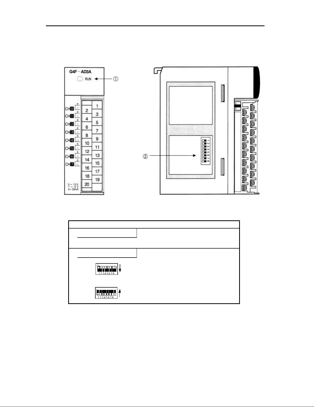
2.3 Names of Parts and Functions ··················································································································2-4
2.3.1 G3F-AD3A ·························································································································································2-4
2.3.2 G4F-AD3A ·························································································································································2-5
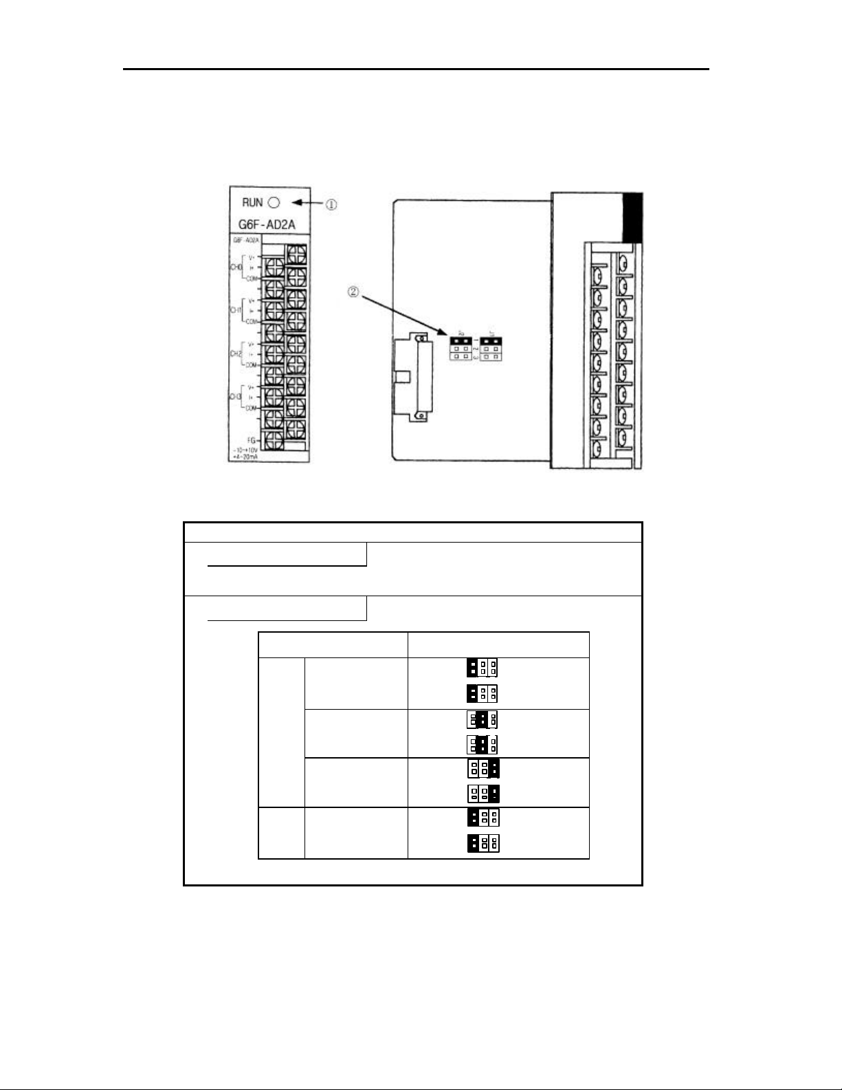
2.3.3 G6F-AD2A ·························································································································································2-6
2.4 I/O Conversion Characteristics ·················································································································2-7
2.4.1 Voltage Input Characteristics ··························································································································2-8
2.4.2 Current Input Characteristics ··························································································································2-10
2.4.3 Simultaneous Voltage and Current Input Characteristics ················································································2-11
2.4.4 Analog input and Digital output characteristics ·······························································································2- 12
2.5 Processing Specification······························································································································2-13
2.5.1 Sampling processing A/D conversion system ···································································································2- 13
2.5.2 Averaging processing A/D conversion system ·································································································2-13
Chapter 3. INSTALLATION AND WIRING
3.1 Installation ··························································································································································3-1
3.1.1 Installation Ambience··········································································································································3-1
3.1.2 Handling Precautions ········································································································································3-1
Page 5

3.2 Wiring ···································································································································································3-2
3.2.1 Wiring Precautions ············································································································································3-2
3.2.2 Wiring Examples ···············································································································································3-2
Chapter 4. FUNCTION BLOCK
4.1 Registration of the Function Block for the A/D Conversion Module on the GMWIN ·········4-1
4.2 Function Block for Local································································································································4-2
4.2.1 Module Initialization ···········································································································································4 -2
4.2.2 Module Reading - Array Type ···························································································································4-4
4.2.3 Module Reading - Single Type····························································································································4-5
4.3 Remote Function Block ································································································································4-6
4.3.1 Module Initialization ···········································································································································4 -6
4.3.2 Module Reading ··················································································································································4-8
4.4 Errors on Function Block ··························································································································4-10
Chapter 5. GM PROGRAMMING
5.1 Programming for Distinction of A/D Conversion Value····································································5-1
5.2 Programming for Display of A/D Conversion Value and Error Code on BCD Display...·····5-5
5.3 Programming for Loading the A/D Conversion Module on Remote I/O Station ··················5-8
Chapter 6. Buffer Memory
6.1 The configuration of buffer memory·········································································································6-1
6.1.1 G6F-AD2A···························································································································································6-1
6.1.2 G3F-AD3A / G4F-AD3A ······································································································································6-2
6.2 The contents and description of buffer memory·················································································6-3
6.2.1 G6F-AD2A···························································································································································6-3
6.2.2 G3F-AD3A / G4F-AD3A······································································································································6-8
Chapter 7. Buffer read/write instructions
7.1 Buffer read instructions··································································································································7-1
7.1.1 GET/GETP instruction·········································································································································7-1
7.1.2 RGET instruction·················································································································································7-3
7.2 Buffer write instructuins·································································································································7-6
7. 2.1 PUT/PUTP instruction ·········································································································································7-6
7. 2.2 RPUT instruction·················································································································································7-8
Page 6

Chapter 8. MK Programming
8.1 Basic Programming ········································································································································8-1
8.1.1 G6F-AD2A ·························································································································································8-1
8.1.2 G3F-AD3A / G4F-AD3A ····································································································································8-2
8.2 Example Programming ·································································································································8-3
8.2.1 A program for comparision of A/D conversion value ························································································8-3
8.2.2 Output the analog input value by 7-segment display ·······················································································8-5
8.2.3 An A/D module mounted on a remote station ·····································································································8-7
Chapter 9. DIMENSIONS
9.1 G3F-AD3A Dimensions ·································································································································9-1
9.2 G4F-AD3A Dimensions ·································································································································9-2
9.3 G6F-AD2A Dimensions ·································································································································9-3
Page 7

Chapter 1 Introduction
1 Introduction
The G3F-AD3A, G4F-AD3A, and G6F-AD2A modules are analog-to -digital conversion
modules for use with the GLOFA PLC GM1/2/3/4/6 series and MASTER-K PLC
K200S/300S/1000S series. The G3F-AD3A is used with GM1/2/3 series and K1000S
series, G4F-AD 3A is used with GM4 series and K300S series, and G6F -AD2A is used
with GM6 series and K200S series. (Hereafter the G3F-AD3A, G4F-AD3A, and G6FAD2A modules are called as the A/D conversion module)
The A/D conversion module is to convert an analog input sig nal (voltage or current) from
external devices into a 12-bit signed binary digital value.
1.1 Features
1) Multi-channel analog to digital conversion is possible with a single A/D module.
- G6F-AD2A : 4 channels
- G4F-AD3A and G3F-AD3A : 8 channels
2) The select of voltage input or current input is possible by channel of A/D module.
3) The unlimited number of A/D modules can be mounted on a base board.
The maximum number of A/D modules depends on the power capacity of power supply
module.( In case of use to the G6F-AD2A with G6F -DA2V and G6F-DA2I, it is depends
on the power capacity of the GM6 -PAFB)
1-1
Page 8
Chapter 1 Introduction
1.2 Terminology
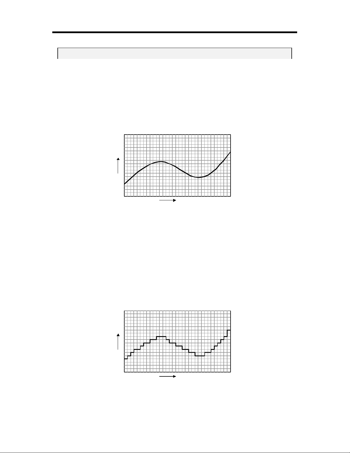
1.2.1 Analog value : A
Analog value is a continuously changing value such as voltage, current, temperature,
speed pressure, flux, etc. Temperatur e, for example, is continuously changing according
to the time. Because this temperature itself is not available for input of the PLC, the
temperature should be converted an analog electrical signal by transducer. Moreover, the
converted analog signal (voltage or current) has to be converted into a digital value with
the A/D module because the PLC can handle only digital values.
value
time
Figure 1.1 Analog value
1.2.2 Digital value : D
Digital value is a discrete data that are described in numbers such as 0, 1, 2, … In
general, a binary code system that are consist of 0(off) and 1(on) is used for expressing
digital value. Also, BCD or hexadecimal values are used.
Because the CPU module of PLC can handle dig ital value only, the analog signal from
external devices should be converted into analog signals with A/D module.
In the other hand, the digital output of CPU module should be converted into analog
signal to be used for external devices. The D/A module (digital-analog converter) is used
for converting digital values into analog output (voltage or current).
value
time
Figure 1.2 Digital value
1-2
Page 9

Chapter 1 Introduction
5V
Analog input voltage
1.3 Analog -to-Digital conversion characteristics
1.3.1 Voltage input
The A/D module converts the analog input from external devices to the digital value that
can be handled by CPU module.
When the analog input is voltage input, the K4F-AD3A and K7F-AD3A has two input
ranges such as 1 ~ 5VDC and 0 ~ 10VDC. The K3F-AD2A has three input range such as
1 ~ 5VDC, 0 ~ 10VDC, and –10 ~ 10VDC.
With all analog input range, the digital output is varied in the range of 0 ~ 4000. Therefore,
the resolution of the A/D module is obtained by following equation;
module A/DofResolution
=
−
voltage inputMinimumvoltageinputMaximum
4000
1) 1 ~ 5VDC range
When the A/D module operates with 1 ~ 5VDC range, the 1VDC analog input is
converted to digital 0, and the 5VDC analog input is converted into digital output 4000.
Therefore, the resolution per 1 digital value is 0.001VDC.
4000
2000
Digital output value
0
1V
2002
2001
2000
1999
1998
3V
2.998V
2.999V
Figure 1. 3 A/D conversion characteristics ( 1 ~ 5VDC )
3.000V
3.002V
3.001V
1-3
Page 10
Chapter 1 Introduction
2) 0 ~ 10VDC range
When the A/D module operates with 0 ~ 10VDC range, the 0VDC analog input is
converted to digital 0, and the 10VDC analog input is converted into digital output 40 00.
Therefore, the resolution per 1 digital value is 0.0025VDC.
4000
2002
2001
2000
2000
Digital output value
0
0V
Analog input voltage
5V
10V
1999
1998
4.995V
5.000V
Figure 1.4 A/D conversion characteristic ( 0 ~ 10VDC )
3) –10 ~ 10VDC range
When the A/D module operates with –10 ~ 10VDC range, the 10VDC analog input is
converted to digital 0, and the 10VDC analog input is converted into digital output 4000.
Therefore, the resolution per 1 digital value is 0.005VDC.
5.005V
5.0025V4.9975V
4000
2002
2001
2000
Digital output value
2000
1999
0
-10V
0V
Analog input voltage
10V
1998
-0.010V
-0.005V
0.010V
0.005V
0.000V
Figure 1.5 A/D conve rsion characteristic ( -10 ~ 10VDC )
1-4
Page 11

Chapter 1 Introduction
1.3.2 Current input
When the analog input is current input, the A/D conversion module has only one input
ranges such as 4 ~ 20mA.
With all analog input range, the digital output is varied in the range of 0 ~ 4000. Therefo re,
the resolution of the A/D module is obtained by following equation;
moduleA/DofResolution
=
−
currentinputMinimumcurrentinputMaximum
4000
1) 4 ~ 20mA range
When the A/D module operates with 4 ~ 20mA range, the 4mA analog input is converted
to digital 0, and the 20mA analog input is converted into digital output 4000. Therefore,
the resolution per 1 digital value is 0.004mA.
4000
2000
Digital output value
0
4mA
12mA 20mA
Analog input current
2002
2001
2000
1999
1998
11.992mA
11.996mA
12.000mA
12.004mA
12.008mA
Figure 1.6 A/D conversion characteristic ( 4 ~ 20mA )
1-5
Page 12
Chapter 2. SPECIFICATIONS
Operating ambient
temperature
Storage ambient
Operating ambient
humidity
10≤f∠57 Hz
57≤f≤150 Hz
9.8㎨ (1G)
10≤f∠57 Hz
57≤f≤150 Hz
4.9㎨(0.5G)
IEC 61131-2
IEC1000-4-3
Chapter 2 . SPECIFICATIONS
2.1 General Specifications
Table 2.1 shows the general specifications of GLOFA GM series and MASTER-K series.
Item Specifications Standard
0 ~ 55℃
temperature
Storage ambient
Humidity
Frequency Acceleration Amplitude
Vibration
Frequency Acceleration Amplitude
*Maximum shock acceleration: 147㎨ {15G}
Shocks
Noise immunity
Operating atmosphere Free from corrosive gases and excessive dust
Altitude for use Up to 2,000m
Pollution degree 2 or lower
Cooling method Self-cooling
*Duration time :11 ms
*Pulse wave: half sine wave pulse( 3 times in each of X, Y and Z directions )
Square wave impulse noise ±1,500 V
Electrostatic discharge Voltage :4kV(contact discharge)
Radiated electromagnetic field 27 ~ 500 MHz, 10 V/m
In case of occasional vibration Sweep count
- 0.075 mm
In case of continuos vibration
- 0.035 mm
Fast transient
&
burst noise
-25 ~ 70℃
5 ~ 95%RH, non-condensing
5 ~ 95%RH, non-condensing
-
-
Modules
Voltage 2 kV 1 kV 0.25 kV
All power
modules
Digital I/O s
( Ue≥ 24 V)
10 times in each
direction for
X, Y, Z
Digital I/Os
(Ue < 24 V)
Analog I/O s
communication
I/Os
IEC 61131-2
IEC 61131-2
LGIS
Standard
IEC 61131-2
IEC1000-4-2
IEC 61131-2
IEC1000-4-4
[Table 2.1 ] General specifications
REMARK
1) IEC(International Electrot echnical Commission)
: The international civilian organization which produces standards for electrical and electronics industry.
2) Pollution degree
: It indicates a standard of operating ambient pollution level.
The pollution degree 2 means the condition in which normally, only non-conductive pollution occurs.
Occasionally, however, a temporary conductivity caused by condensation shall be expected.
2 - 1
Page 13
Chapter 2. SPECIFICATIONS
2.2 Performance Specifications
Table 2-2 shows performance specifications of A/D conversion modul e.
1) G3F -AD3A, G4F-AD3A
Analog
input
Maximum
resolution
Items
Specifications
G3F-AD3A G4F-AD3A
I/O points 16 points
Voltage
Current
- Adjust input selection switch for each channel on side of module.
Voltage/Current selection
Digital output - 16 bit binary value
1 ~ 5VDC 1 mV (1/4000)
0 ~ 10VDC 2.5 mV (1/4000)
DC 4 ~20mA
Overall Accuracy
( ON : Current, OFF : Voltage)
- Selection of voltage range by program
1 ~ 5 VDC (input resistance 600㏀)
0 ~ 10 VDC (input resistance 600㏀)
DC 4 ~ 20 mA (input resistance 250Ω)
4㎂ (1/4000)
±0.5% (accuracy to full scale)
Max . conversion speed 5.0 ms/channel
Max . absolute input Voltage : 15V, Current : 25mA
Number of analog input point 8 channels/module
Isolation
Terminals connected 20-point terminal block
Internal current consumption 0.5 A 0.5 A
Weight 310 280
Between input terminals and PLC: Photo coupler isolation
(Between channels : Non-isolated)
[Table 2.2] Performance Specifications
CAUTION
The manufacturer set value of A/D conversion module has been current input mode.
2 - 2
Page 14
Chapter 2. SPECIFICATIONS
2) G6F-AD2A
Items Specifications
I/O points 16 points
Voltage
Analog
input
Current
Voltage/Current selection
1 ~ 5 VDC (input resistance 1㏁)
0 ~ 10 VDC (input resistance 1㏁)
-10 ~ 10VDC (input resistance 1㏁)
DC4 ~ 20 mA (input resistance 250Ω)
- Selection with Terminal
( It has to be connected between V and I terminal to select current. )
- Selection of voltage range by switch on the side of module
Digital output
1 ~ 5VDC 1 mV (1/4000)
Maximum
resolution
Overall Accuracy
Max . conversion speed 5.0 ms/channel
Max . absolute input Voltage : 15V, Current : 25mA
Number of analog input point 4 channels/module
Terminals connected 18-point terminal block
Current
Consumption
0 ~ 10VDC 2.5 mV (1/4000)
-10 ~10VDC 5 mV (1/4000)
DC 4 ~20mA
Isolation
+5VDC
+15VDC
-15VDC
Weight
- 12 bit binary value( -48 ~ 4047, -2048 ~ 2047)
-
Digital output value is selected by program.
4㎂ (1/4000)
±0.5% (accuracy to full scale)
Between input terminals and PLC: Photo coupler isolation
(Between channels : Non-isolated)
40mA
50mA
20mA
200g
[Table 2.2] Performance Specifications
CAUTION
The factory-set value of A/D conversion module has been current input mode.
The G6F-AD2A has to be used with the GM6-PAFB.
2 - 3
Page 15
Chapter 2. SPECIFICATIONS
2.3 Names of Parts and Functions
The names of parts and functions of the A/D conversion module are shown as below.
2.3.1 G3F-AD3A
2 - 4
Page 16
Chapter 2. SPECIFICATIONS
2.3.2 G4F-AD3A
No Description
←
RUN LED
Indicates the operating status of the G3F-AD3A and G4F-AD3A.
Selection switch of voltage/current
↑
1)The switch status at voltage selection
The switch locates off status.
2)The switch statues at current selection
The switch locates on status
2 - 5
Page 17
Chapter 2. SPECIFICATIONS
1 23
J1
J1
J2
1
2
3
2.3.3 G6F-AD2A
No Description
←
RUN LED
Indicates the operating status of the G6F-AD2A.
Selection switch of voltage/current
↑
Analog Input Input Range Selection Switch
DC 1~5V
Voltage
DC 0~10V
DC-10~10V
Current DC 4~20mA
J2
1 2 3
J1
1 2 3
J2
J1
J2
2 - 6
Page 18
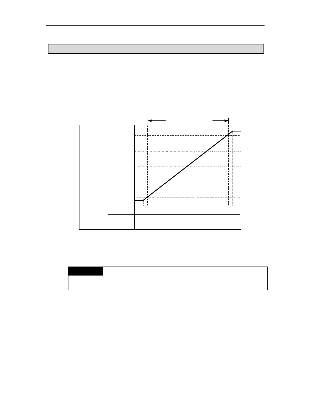
Chapter 2. SPECIFICATIONS
2.4 I/O Conversion Characteristics
Digital
4000
3000
2000
0
0V
5V
10V1V3V
5V
Analog
-0.12V
3.808
0.952V
10.12V
20.192
㎃
5.048V
4047
-48
Input / Output (hereafter I/O) conversion characteristics are expressed with the angle of the line between
analog input(voltage and current) and matched digital value.
I/O conversion characteristics of the G3F-AD3A, G4F-AD3A are expressed with Fig 2.1, and I/O conversion
characteristics of the G6F-AD2A is expressed with Fig 2.2
The voltage or current input for a channel is selected by analog input selection switch and the value of
Offset / Gain can not be changed because it is fixed.
Practical analog input range
Output
Value
1000
Input
DC 0 ~ 10V
DC 1 ~ 5V
DC 4 ~ 20㎃
㎃
4 ㎃ 12㎃ 20 ㎃
REMARK
1. The analog output value of over 4047 or –48 is fixed as 4047 or –48.
2. Keep the input voltage and current not to exceed +15V and 25mA.
[Fig 2.1] I/O Conversion Characteristics
2 - 7
Page 19
Chapter 2. SPECIFICATIONS
Input selection switch
- Off : Voltage
(This switch is located
On
Digital
1000
0V5V10V 1V3V
5V
Analog
-0.12V
-10.24V
0.952V
10.12V
10.24V
5.048V
48
3.808㎃20.192
2000
1000
0
2047
Practical analog input range
4047
4000
3000
Output
2000
Value
-1000
0
-
-10V
4㎃ 12 ㎃ 20㎃DC 4 ~ 20 ㎃
0V 10V
Input
-2000
-2048
DC 0 ~ 10V
DC 1 ~ 5V
DC-10 ~ 10V
[Fig 2.1] I/O Conversion Characteristics
REMARK
1. The analog output value of over 4047 or –48(2047 or –2048) is fixed as 4047 or –48(2047 or –2048).
2. Keep the input voltage and current not to exceed +15V and 25mA.
2.4.1 Voltage Input Characteristics
1) G3F -AD3A, G4F-AD3A
For voltage input, the corresponding input selection switch of each channel should be set to "off".
–
The voltage input range is selected in program.
Input selection switch has to be located at off.
(1)Voltage input range : DC 0 ~10V
Digital output value for input voltage is shown as follows.
1 2 3 4 5 6 7 8
on the side of module)
CH0 1234567 Number of channel
Analog input voltage (V)
- 0.12 0 2.5 5 7.5 10 10.12
㎃
Digital output value -48 0 1000 2000 3000 4000 4047
2 - 8
Page 20
Chapter 2. SPECIFICATIONS
12
J2
1 2 3
11
12 1 2 3 J1
J2 1 2
3J1J2
(2)Voltage input range : DC 1 ~5V
Digital output value for input voltage is shown as follows.
Analog input voltage (V)
0.952 1 2 3 4 5 5.048
Digital output value -48 0 1000 2000 3000 4000 4047
2) G6F-AD2A
For voltage input, the corresponding input is selected by selection switch and selected input voltage range is
same through whole channels.
1) Voltage input range
: DC 1 ~5V
Digital output value for input voltage is shown as follows.
Analog input voltage (V)
0.952 1 2 3 4 5 5.048
Digital output value
-48 0 1000 2000 3000 4000 4047
-2048 -2000 -1000 0 1000 2000 2047
2)
Voltage input range :
DC 0
~ 10
V
Digital output value for input voltage is shown as follows.
Analog input voltage (V)
-0.12 0 2.5 5 7.5 10 10.12
Input range selection
switch
11
J1
1 2 3
1 2 3
Input range selection
switch
Digital output value
-48 0 1000 2000 3000 4000 4047
-2048 -2000 -1000 0 1000 2000 2047
3)
Voltage input range :
DC - 10
~ 10
V
Digital output value for input voltage is shown as follows.
Analog input voltage (V)
Input range selection
switch
-10.24 -10 -5 0 5 10 10.24
Digital output value
-48 0 1000 2000 3000 4000 4047
-2048 -2000 -1000 0 1000 2000 2047
2 - 9
Page 21
Chapter 2. SPECIFICATIONS
On
- On : Current
(This switch is located
1 2 3
11
12 1 2
3
J1
J2
2.4.2
Current Input Characteristics
1) G3F-AD3A, G4F-AD3A
For current input, the corresponding input selection switch of each channel should be set to "on".
Input selection switch
1 2 3 4 5 6 7 8
CH0 1234567
on the side of module)
Number of channel
- Digital output value for input current is shown as follows.
Analog input current(㎃)
3.808 4 8 12 16 20 20.192
Digital output value -48 0 1000 2000 3000 4000 4047
2) G6F-AD2A
Digital output value for input voltage is shown as follows.
Analog input current (mA)
3.808 4 8 12 16 20 20.192
Digital output value
-48 0 1000 2000 3000 4000 4047
-2048 -2000 -1000 0 1000 2000 2047
It has to be connected between V and I terminal to select current.
Input range selection
switch
2 - 10
Page 22
Chapter 2. SPECIFICATIONS
On
- On : Current
1
2
3
J1
J2
V+
I+
COM + Analog Input
V+
I+
COM + Analog Input
2.4.3
Simultaneous Voltage and Current Input Characteristics
1) G3F- AD3A, G4F-AD3A
For simultaneous voltage and current input, the input conversion switch of each channel is set to corresponding
voltage and current range.
Ex) Voltage input range: 0 to 3 Current input range: 4 to 7
Input selection switch
- Off : Voltage
1 2 3 4 5 6 7 8
CH 0 1234567
(제품의 좌측면에 위치)
채널 번호
- Digital output value for analog input is shown as follows..
Analog input
Voltage
(V)
Current
(mA)
0~10V
1~ 5V
4 ~ 20 mA
-0.12 0 2.5 5 7.5 10 10.12
0.952 1 2 3 4 5 5.048
3.808 4 8 12 16 20 20.192
Digital output value -48 0 1000 2000 3000 4000 4047
2) G6F-AD2A
For simultaneous use of voltage and current input, the available input voltage rage is 0 ~ 5VDC only.
Digital output value for analog input is shown as follows..
Analog input
Voltage DC1~ 5V
Current DC4 ~ 20mA
Digital output value
0.952 1 2 3 4 5 5.048
3.808 4 8 12 16 20 20.192
-48 0 1000 2000 3000 4000 4047
-2048 -2000 -1000 0 1000 2000 2047
Ex) channel for voltage : 0, channel for current : 1
Input Rage Selection Switch
Wiring Example
Voltage Input(Channel “0”) Current Input(Channel ”1”)
2 - 11
Page 23
Chapter 2. SPECIFICATIONS
Analog input and Digital output
Analog input and digital output value
2000
2001
2002
2004
2005
2006
2007
2008
2009
Digital output value
2000
2001
2002
2004
2005
2006
2007
2008
2009
2.4.4 Analog input and Digital output characteristics
1) G3F-AD3A, G4F-AD3A
Digital output value
No
DC 0~10V 2.5 mV
ℵ
ℑ
ℜ
2) G6F-AD2A
Input
range
DC 1~5V 1mV
DC 4~20
㎃
Digital
output
value
0
~
4000
Resolution Analog input value
4 ㎂
3.000
~
3.001
12.000
~
12.004
5.000
~
5.0025
3.001
~
3.002
12.004
~
12.008
3.002
~
3.003
12.008
~
12.012
5.0025
5.005
3.003
~
3.004
12.012
~
12.016
~
② ③
3.004
~
3.005
12.016
~
12.020
3.005
~
3.006
12.020
~
12.024
5.005
~
5.0075
3.006
3.007
12.024
12.028
①
5.0075
~
5.010
3.007
3.008
~
~
3.008
12.028
~
~
12.032
~
3.009
12.032
~
12.036
3.009
~
3.010
12.036
~
12.040
③ ④
②
①
Digital
No Input range
Resolution Analog input value
output
value
DC-10~10V 5mV
ℵ
0 ~
DC 0~10V 2.5 mV
ℑ
4000
or
-2048
DC 1~5V 1mV
ℑ
~
2047
DC 4~20 ㎃
ℜ
4 ㎂
3.000
~
3.001
12.000
~
12.004
5.000
~
5.0025
3.001
~
3.002
12.004
~
12.008
0.000
~
0.005
3.002
~
3.003
12.008
~
12.012
5.0025
5.005
3.003
~
3.004
12.012
~
12.016
~
3.004
~
3.005
12.016
~
12.020
5.005
5.0075
3.005
~
3.006
12.020
~
12.024
~
3.006
~
3.007
12.024
~
12.028
0.005
~
0.010
3.007
~
3.008
12.028
~
12.032
5.0075
5.010
3.008
~
3.009
12.032
~
12.036
~
3.009
~
3.010
12.036
~
12.040
2 - 12
Page 24

Chapter 2. SPECIFICATIONS
2.5 Processing specifications
2.5.1 Sampling processing A/D conversion system
The anal og values input to the channels designated for sampling processing by the CPU are
converted to digital output values one by one and the digital output values are stored in the
buffer memory.
As the A/D module scans each channel, the value appearing at the instant is written to the
buffer memory as a digital value. The timing of this sampling depends on the number of
channels used, and may be found from the following expression.
Process time = Number of channels used × Maximum conversion time (5 ms)
The process time when 4 channels is used, for example, will be 20 msec = 4 × 5 ms
2.5.2 Averaging processing A/D conversion system
The A/D module makes the A/D conversion for any channels to which averaging processing
has been specified from the CPU. Using a preset count, an average is calculated (excluding the
maximum value and the minimum value) and stored to the buffer memory. The preset count
can be set as 2 to 255 times.
The time in which the average value by this processing is stored in the buffer memory varies
with the number of channels used.
Processing time = Count setting × No. of channels × 5ms (Max conversion time)
The processing time when count value is 50 and 4 channels are used, for example, will be 50 ×
4 × 5ms = 1000ms.
2 - 13
Page 25

Chapter 3 Installation and wiring
3 Installation and wiring
3.1 Installation
3.1.1 Installation ambiance
The A/D module has designed to have high reliability regardless of its installation
ambiance. However, please be sure to check the following precautions for higher
reliability and stability of system.
1) Ambiance requirements
Avoid installing the A/D module in following locations where;
① temperature may experience ambient drops or rising.
(It should stay within 0 °C ~ 55 °C or 32 °F ~ 131 °F)
② condensation may occur due to abrupt temperature changes
③ vibration and shock are directly transmitted to the PLC system.
④ the PLC system is exposed to the direct rays of the sun.
⑤ the PLC system is exposed to corrosive or inflammable gas.
⑥ the PLC system is exposed to conductive powder, oil mist, salt, or organic solvent.
2) Installing and wiring
① During wiring or other work, do not allow any wire scraps to enter into the module.
② Install the module on location that is convenient for operation.
③ Be sure that it is not located near high voltage equipment on the same panel.
④ Be sure to install the module at least 50 mm away from a duct or other devices.
⑤ Be sure to be grounded to locations that have good noise immunity.
3.1.2 Handling precautions
From unpacking to installation, be sure to check the following;
①
Do not drop it off, and make sure that strong impacts should not be applied.
② Do not dismount printed circuit boards from the case. It can cause malfunctions of
module.
③ Be sure to disconnect electrical power before mounting / dismounting the module.
3 - 1
Page 26

Chapter 3 Installation and wiring
R
- 15V
+15V
J1
J2
FG
V+
R R R R R
V+
- 15V
+15V
1 2 3
J2
FG
V+
R R R
R
*1
*1
3.2 Wiring
3.2.1 Wiring precautions
① Separate AC and external input signal of A/D module wiring not to be affected by
surge or induced noise in the AC.
② External wiring has to be at least AWG32 (0.3mm2 ), and be selected in consideration
of operating ambiance and/or allowable current.
③ Separate wiring from device and/or substances generating intense heat, and oil not to
make short-circuit which leads to damage and/or mis-operation.
④ Be careful not to connect external power supply with wrong polarity.
⑤ Separate external wiring sufficiently from high voltage and power supply cable not to
cause induced noise or malfunction of module.
3.2.2 Wiring examples
1) G6F-AD2A
① Voltage input
I+
COM
Input Range
Selection Switch
1 2 3
I+
COM
G6F -AD2A
② Current input
Input Range
COM
I+
Selection Switch
J1
V+
COM
I+
G6F -AD2A
*1: Use a two -core twisted pair shielded cable
*2 : If noise is expected, ground the cable and FG terminal as shown in figure.
3 - 2
Page 27

Chapter 3 Installation and wiring
R
CH7
CH0
selection switch
*1
R
R
R
R
R
selection switch
R
R
CH7
CH0
selection switch
R
R R R R R
R
2) G3F-AD3A / G4F -AD3A
① Voltage input
② Current input
Voltage/current
Voltage/current
Voltage range
Voltage range
*1: Use a two-core twisted pair shielded cable
*2 : If noise is expected, ground the cable as shown in figure.
3 - 3
Page 28

Chapter 4. FUNCTION BLOCK
4 .1 Registration of the Function Block for A/D Conversion Module on the GMWIN
Library Insertion(I)
G3F – AD3A
. ADR3RD
G4F – AD3A
. ADR3RD
Function block
Function block
G6F – AD2A
Function block
CHAPTER 4. FUNCTION BLOCK
This shows function block for A/D conversion module on the GMWIN.
A kind of function block is as follows.
G3F-AD3A G4F-AD3A G6F-AD2A
No
Function
Local Remote Local Remote Local Remote
1 AD3INI ADR3INI AD3INI ADR3INI AD2INI ADR62 INI Initializing module
2 AD3ARD ADR3RD AD3ARD ADR3RD AD2ARD ADR62RD Reading A/D converted value(array Type)
3 AD3RD - AD3RD - AD2RD - Reading A/D converted value(Single Type)
The function block type and functions of input/output parameters of G3F -AD3A and G4F-AD3A are same.
Function Block is inserted on the execution of the GMWIN according to following procedure.
Function block can be inserted only in the open condition of the Project.
select
Project(P)
1. Special.3fb
. AD3INI
. AD3ARD
. AD3RD
2. Remote3.3fb
. ADR3INI
. ADR3RD
3. Remote4.3fb
. ADR3INI
Insertio n for Local
Function block
insertion
for Remote GM3
Function block
insertion
for Remote GM4
1. Special.4fb
. AD3INI
. AD3ARD
. AD3RD
2. Remote4.4fb
. ADR3INI
. ADR3RD
3. Remote3.4fb
. ADR3INI
insertion
for Local
Function block
insertion
for Remote GM4
Function block
insertion
for Remote GM3
1. Special.6fb
. AD2INI
. AD2ARD
. AD2RD
2. Remote6.6fb
. ADR62INI
. ADR62RD
insertion
for Local
Function block
insertion
for Remote GM6
4 - 1
Page 29

Chapter 4. FUNCTION BLOCK
4 .2 Function Block for Local
4.2.1 Module Initialization
1) G3F-AD3A, G4F-AD3A
Module Initialization function block is used in a program with setting of A/D conversion module located
base number, slot number of located module on base, specifying a channel enable, analog input data
type and the information of average processing.
Function
block
AD3INI
REQ
BASE
SLOT
CH
TYPE
AVG_
AVG_
DONE
STAT
ACT
I/O Variable
Input
REQ BOOL
BASE USINT
SLOT USINT
CH BOOL[8]
TYPE BOOL[8]
AVG_
EN
AVG_
NUM
Output
DONE BOOL
STAT USINT
ACT BOOL[8]
REMARK
BOOL[8] and USINT[8] of data type means that the number of element is 8, and also this means the whole number of channels and channel
number.
Data
type
BOOL[8]
USINT
[8]
Descriptions
Function Block Execution Request Area
- The execution of function block initialization is requested in this area.
- If the status of condition connected with this area is changed from low(0) to high(1),
function block initialization for the module is executed.
Base Location Number Area
- The base No. on which A/D conversion module is mounted is written on this area.
- Setting range : 0 to 3
Slot Location Number Area
- The slot No. on which A/D conversion module is mounted is written on this area.
- Setting range: 0 to 7
Available Channel Specification Area
- Enabled channels are specified to 1 and disabled channels are specified to 0.
Analog Input Data Type Specification Area
- Output digital data type for each channel is specified in this area.
- 0 is for the range of 1 ~ 5VDC and DC4 ~ 20mA.
- 1 is for the range of 0 ~ 10VDC
Enable / Disable of Average processing
- 0 is for the sampling processing.
- 1 is for the average processing of the number of times.
Set a constant of the average processing of the number of times.
- Setting range : 2 ~ 255
Function Block Execution Complete Area
- When function block initialization is executed with no error, 1 is written and until
next execution, 1 is continuing. When error occurs, 0 is written and operation come
to stop.
Error Code Display Area
- When error occurs during function block initialization, the error code number is
written.
Channel Operation Display Area
- After execution the function block of initialization with no error, if the setting
condition of specified channel is normal then output ‘1’, or if abnormal, output 0’.
- No specified channel is ‘0’.-
4 - 2
Page 30

Chapter 4. FUNCTION BLOCK
TYPE
2) G6F-AD2A
Module Initialization function block is used in a program with setting of A/D conversion module located
base number, slot number of located module on base, specifying a channel enable, analog input data
type and information of average processing .
Function
block
AD2INI
REQ
BASE
SLOT
CH
DATA
AVG_
AVG_
DONE
STAT
ACT
I/O Variable
Input
Data
type
REQ BOOL
BASE USINT
SLOT USINT
CH BOOL[4]
DATA
TYPE
AVG_
EN
AVG_
NUM
BOOL[ 4]
BOOL[4]
USINT[4]
Descriptions
Function Block Execution Request Area
- The execution of function block initialization is requested in this area.
- If the status of condition connected with this area is changed from low(0) to high(1),
function block initialization for the module is executed.
Base Location Number Area
- The base No. on which A/D conversion module is mounted is written on this area.
- Setting range : 0
Slot Location Number Area
- The slot No. on which A/D conversion module is mounted is written on this area.
- Setting range: 0 to 7
Available Channel Specification Area
- Enabled channels are specified to 1 and disabled channels are specified to 0.
Digital Output Data Type Specification Area
- 0 is for the range of –48 ~ 4047
- 1 is for the range of –2048 ~ 2047
Enable / Disable of Average processing
- 0 is for the sampling processing.
- 1 is for the average processing for the number of times.
Set a constant of the average processing of the number of times.
- Setting range : 2 ~ 255
Output
DONE BOOL
STAT USINT
ACT BOOL[4]
Function Block Execution Complete Area
- When function block initialization is executed with no error, 1 is written and 1 is
kept until next execution. When error occurs, 0 is written and operation come to
stop.
Error Code Display Area
- When error occurs during function block initialization, the error code number is
written.
Channel Operation Display Area
- The channel specified after executing the function block initialization with no error
is right, 1 is written and, on the non -specified channel, 0 is written.
REMARK
BOOL[4] and USINT[4] of data type means that the number of element is 4, and also this means the whole number of channels and channel
number.
4 - 3
Page 31

Chapter 4. FUNCTION BLOCK
4.2.2 Module Read ing-Array Type
1) G3F-AD3A, G4F-AD3A
Array type of function block for reading the module is performed for every channel in block and the specified
channels are used to read output variable of data displayed from A/D conversion digital value.
Function
REQ
BASE
SLOT
CH
block
AD3ARD
DONE
STAT
ACT
DATA
I/O Variable
Input
output
REQ BOOL
BASE USINT
SLOT USINT
CH BOOL[8]
DONE BOOL
STAT USINT
ACT BOOL[8]
DATA INT[8]
REMARK
BOOL[8] and USINT[8] of data type means that the number of element is 8, and also this means the whole number of channels and channel number.
2) G6F-AD2A
Array type of function block for reading is performed for all channels in module and the specified
channel is used to read output variable of data displayed from A/D conversion digital value.
Function
REQ
BASE
SLOT
CH
block
AD2ARD
DONE
STAT
ACT
DATA
I/O Variab le
Input
Output
REQ BOOL
BASE USINT
SLOT USINT
CH BOOL[4]
DONE BOOL
STAT USINT
ACT BOOL[4]
DATA INT[4]
Data
type
Function Block Execution Request Area
- The execution of function block reading is requested in this area.
- If the status to be connected with this area is satisfied on the program operation
and input condition changes from low(0) to high(1), function block initialization for
the module is executed.
Base Location Number Area
- The base No. on which A/D conversion module is mounted is written on this area.
- Setting range : 0 to 3
Slot Location Number Area
- The slot No. on which A/D conversion module is mounted is written on this area.
- Setting range: 0 to 7
Available Channel Specification Area
- Enabled channels are specified to 1 and disabled channels are specified to 0.
Function Block Execution Complete Area
- When function block reading is executed with no error, 1 is written and until next
execution, 1 is continuing. When error occurs, 0 is written and operation come to
stop
Error Code Display Area
- When error occurs during function block reading, the error code number is written.
Channel Operation Display Area
- After execution the function block of initialization with no error, if the setting
condition of specified channel is normal then output ‘1’, or if abnormal, output 0’.
- No specified channel is ‘0’.-
A/D Conversion Value Output Area
Output data range : -48 ~ 4047
Data
type
Function Block Execution Request Area
- The execution of function block reading is requested in this area.
- If input condition is changed from low(0) to high(1), function block initializatio n for
the module is executed.
Base Module Location Number Area
- The base No. on which A/D conversion module is mounted is written on this area.
- Setting range : 0
Slot Location Number Area
- The slot No. on which A/D conversion module is mounted is written on this area.
- Setting range: 0 to 7
Available Channel Specification Area
- Available channels are specified in this area.
- Enabled channels are specified to 1 and disabled channels are specified to 0.
Function Block Execution Complete Area
- When function block reading is executed with no error, 1 is written and 1 is kept
until next execution. When error occurs, 0 is written and operation come to stop
Error Code Display Area
- When error occurs during function block reading, the error code number is written.
- Error code is referred to Manual 4.3.
Channel Operation Display Area
- The channel specified after executing the function block read with no error is
right, 1 is written and, on the non -specified channel, 0 is written
A/D Conversion Value Output Area
- Output data range : -48 ~ 4047 or –2048 ~ 2047
Descriptions
Descriptions
4 - 4
Page 32

Chapter 4. FUNCTION BLOCK
4.2.3 Module Read ing - Single Type
1) G3F-AD3A, G4F-AD3A
Single type of func tion block for reading the module is performed for only one channel and the specified
channel is used to read output variable of data displayed from A/D conversion digital value.
Function
block
I/O Variable
Input
AD3RD
REQ
DONE
STAT
BASE
DATA
SLOT
CH
output
2) G6F-AD2A
Single type of function block for reading the module is performed for only one channel and the specified
channel is used to read output variable of data displayed from A/D conversion digital value.
Function
REQ
BASE
SLOT
CH
block
AD2RD
DONE
STAT
DATA
I/O Variable
Input
Output
Data
type
REQ BOOL
BASE USINT
SLOT USINT
CH USINT
DO NE BOOL
STAT USINT
DATA INT
Data
type
REQ BOOL
BASE USINT
SLOT USINT
CH BOOL[4]
DONE BOOL
STAT USINT
DATA INT[4]
Descriptions
Function Block Execution Request Area
- The execution of function block reading is requested in this area.
- If the status to be connected with this area is satisfied on the program operation and
input condition changes from low(0) to high(1), function block initialization for the
module is executed.
Base Module Location Number Area
- The base No. on which A/D conversion module is mounted is written on this area.
- Setting range : 0 ~ 3
Slot Location Number Area
- The slot No. on which A/D conversion module is mounted is written on this area.
- Setting range: 0 to 7
Available Channel Specification Area
- Enabled channels are specified to 1 and disabled channels are specified to 0.
Function Block Execution Complete Area
- When function block reading is executed with no error, 1 is written and until next
execution, 1 is continuing. When error occurs, 0 is written and operation come to stop.
Error Code Display Area
- When error occurred during function block initialization, the error code number is
written.
A/D Conversion Value Output Area
Output data range : -47 ~ 4048
Descriptions
Function Block Execution Request Area
- The execution of function block reading is requested in this area.
- If input condition is changed from low(0) to high(1), function block initialization for
the module is executed.
Base Module Location Number Area
- The base No. on which A/D conversion module is mounted is written on this area.
- Setting range : 0
Slot Location Number Area
- The slot No. on which A/D conversion module is mounted is written on this area.
- Setting range: 0 to 7
Available Channel Specification Area
Setting range : 0 ~ 3
Function Block Execution Complete Area
- When function block reading is executed with no error, 1 is written and 1 is kept
until next execution. When error occurs, 0 is written and operation come to stop
Error Code Display Area
- When error occurs during function block reading, the error code number is written.
- Error code is referred to Manual 4.3.
A/D Conversion Value Output Are a
- Output data range : -48 ~ 4047 or –2048 ~ 2047
4 - 5
Page 33

Chapter 4. FUNCTION BLOCK
4.3 Remote Function Block
EN
NDR
4.3.1 Module Initialization
1) G3F-AD3A, G4F-AD3A
Module Initialization function block is a program for the use in setting the location number of the slot on
which the communi cation module of A/D conversion module of the master station is mounted, the address
number of communication module which a remote I/O station has, the base location number, and the slot
location number, and specifying the an available channel enable, a data type for A/D conversion, and
average process data.
Function
block
ADR3INI
REQ
NET_
NO
ST_N
O
BASE
SLOT
CH
TYPE
AVG_
AVG_
NUM
ERR
STAT
ACT
I/O Variable
Input
Output
REQ BOOL
NET_
NO
ST_NO USINT
BASE USINT
SLOT USINT
CH BOOL[8]
TYPE BOOL[8]
AVG_
AVG_
NUM
NDR BOOL
ERR BOOL
STAT USINT
ACT BOOL[8]
EN
REMARK
BOOL[8] and USINT[8] of data type means that the number of element is 8, and also this means the whole number of channels and channel number.
Data
type
USINT
BOOL[8]
USINT[8]
Descriptions
Function Block Execution Request Area on Rising Edge.
- The execution of write function block is requested in this area.
- If the status to be connected with this area is satisfied on the program operation and input
condition changes from low(0) to high(1), function block initialization for the module is
executed.
The location number of the slot on which the transmission module of the master station is
mounted. -Setting range: 0 to 7
Station number of the communication module which a remote I/O station has.
- Setting range : 0 to 63
Base Location Number Area
- The base No. on which A/D conversion module is mounted is written on this area.
- Setting range : 0 to 3
Slot Location Number Area
- The slot No. on which A/D conversion module is mounted is written on this area.
- Setting range: 0 to 7
Available Channel Specification Area
- Available channels are specified in this area.
- Enabled channels are specified to 1 and disabled channels are specified to 0.
Output Data Type Specification Area
- Output digital data type for each channel is specified in this area.
- 0 is for the range of 1 ~ 5V DC and DC 4 ~ 20mA
- 1 is for the range of 0 ~ 10V DC
Average Process Enable Specification Area
- 1 is for the average processing. - 0 is for the sampling process.
Set a constant of the average processing of the number of times.
- Setting range : 2 ~ 255
When function block execution is completed with no error, 1 is written. During the scan which
the execution condition has been made, 1 is continuing and at the next scan. 0 is written.
Error Data Display Area
- When error occurs during function block initialization, 1 is written and the operation comes
to stop. During the scan which the execution condition has been made, 1 is continuing
and at the next scan, 0 is written.
Error Code Display Area
- When error occurs during function block initialization, the error code number is written.
Channel Operation Display Area
- The channel specified after executing the function block initialization with no error is
right, 1 is written and, on the non -specified channel, 0 is written.
4 - 6
Page 34

Chapter 4. FUNCTION BLOCK
DATA
TYPE
EN
NDR
2) G6F-AD2A
Module Initialization function block is a program for the use in setting the location number of the slot on
which the communication module of A/D conversion module of the master station is mounted, the address
number of communication module which a remote I/O station has, the base location number, and the slot
location number, and specifying the an available channel enable, a data type for A/D conversion, and
average process data.
Function
block
ADR62INI
REQ
NET_
NO
ST_N
O
BASE
SLOT
CH
AVG_
AVG_
NUM
I/O Variable
t
Inpu
ERR
STAT
ACT
Output
REQ BOOL
NET_
NO
ST_NO USINT
BASE USINT
SLOT USINT
CH BOOL[4]
DATA
TYPE
AVG_
EN
AVG_
NUM
NDR BOOL
E RR BOOL
STAT USINT
ACT BOOL[4]
REMARK
BOOL[4] and USINT[4] of data type means that the number of element is 4, and also this means the whole number of channels and channel number.
Data
type
USINT
BOOL[4]
BOOL[4]
USINT[4]
Descriptions
Function Block Execution Request Area on Rising Edge.
- The execution of write function block is requested in this area.
- If the status to be connected with this area is satisfied on the program operation and input
condition changes from low(0) to high(1), function block initialization for the module is
executed.
The location number of the slot on which the transmission module of the master station is
mounted. -Setting range: 0 to 7
Station number of the communication module which a remote I/O station has.
- Setting range : 0 to 63
Base Location Number Area
- The base No. on which A/D conversion module is mounted is written on this area.
- Setting range : 0
Slot Location Number Area
- The slot No. on which A/D conversion module is mounted is written on this area.
- Setting range: 0 to 7
Available Channel Specification Area
- Available channels are specified in this area.
- Enabled channels are specified to 1 and disabled channels are specified to 0.
Output Data Type Specification Area
- Output digital data type for each channel is specified in this area.
- 0 is for the range of –48 to 4047. - 1 is for the range of -2048 to 2047.
Average Process Enable Specification Area
- 1 is for the average processing. - 0 is for the sampling process.
Set a constant of the average processing of the number of times.
- Setting range : 2 ~ 255
When function block execution is completed with no error, 1 is written. During the scan which
the execution condition has been made, 1 is continuing and at the next scan. 0 is written.
Error Data Display Area
- When error occurs during function block initialization, 1 is written and the operation comes
to stop. During the scan which the execution condition has been made, 1 is continuing
and at the next scan, 0 is written.
Error Code Display Area
- When error occurs during function block initialization, the error code number is written.
Channel Operation Display Area
- The channel specified after executing the function block initialization with no error is
right, 1 is written and, on the non -specified channel, 0 is written.
4 - 7
Page 35

Chapter 4. FUNCTION BLOCK
ERR
NDR
4.3.2 Module Reading
1) G3F-AD3A, G4F-AD3A
Function block for reading the module is performed for every channel in block and the specified channels
are used to read output variable of data displayed from A/D conversion digital value.
Function
block
I/O Variable
Input
Data
type
REQ BOOL
Descriptions
Function Block Execution Request Area
- The execution of read function block is requested in this area.
- If the status to be connected with this area is satisfied on the program operation
and input condition changes from low(0) to high(1), function block reading for the
module is executed.
REQ
NET_
NO
ST_N
O
BASE
SLOT
CH
ADR3RD
DATA
STAT
Output
NET_
NO
ST_NO USINT
BASE USINT
SLOT USINT
CH BOOL[8]
NDR BOOL
ERR BOOL
USINT
The location number of the slot on which the communication module of the master
station is mounted.
- Setting range: 0 to 7
The station number of the communication m odule which a remote I/O station has.
- Setting range : 0 to 63
Base Module Location Number Area
- The base No. on which A/D conversion module is mounted is written on this area.
- Setting range : 0 to 3
Slot Location Number Area
- The slot No. on which A/D conversion module is mounted is written on this area.
- Setting range: 0 to 7
Available Channel Specification Area
- Available channels are specified in this area.
- Enabled channels are specified to 1 and disabled channels are specified to 0.
When function block execution is completed with no error, 1 is written. During the scan
which the execution condition has been made, 1 is continuing and at the next scan. 0
is written.
Error Data Display Area
- When error occurs during the execution of function block reading, 1 is written and
the operation come s to stop. During the scan which the execution condition has
been made, 1 is continuing and at the next scan, 0 is written.
STAT USINT
ACT BOOL[8]
DATA INT[8]
Error Code Display Area
- When error occurs during the execution of function block reading, the error code
number is written.
Channel Operation Display Area
- The channel specified after executing the function block reading with no error is
right, 1 is written and, on the non-specified channel, 0 is written.
A/D Conversion Value Output Area
- Output data range : -48 ~ 4047 or –2048 ~ 2047
REMARK
BOOL[8] and USINT[8] of data type means that the number of element is 8, and also this means the whole number of channels and channel number.
4 - 8
Page 36

Chapter 4. FUNCTION BLOCK
O
ERR
NDR
2) G6F-AD2A
Function block for reading the module is performed for every channel in block and the specified channels
are used to read output variable of data displayed from A/D conversion digital value.
Function
block
I/O Variable
Input
Data
type
REQ BOOL
Descriptions
Function Block Execution Request Area
- The execution of read function block is requested in this area.
- If the status to be connected with this area is satisfied on the program operation
and input condition changes from low(0) to high(1), function block reading for the
module is executed.
REQ
NET_
NO
ST_N
BASE
SLOT
CH
ADR62RD
DATA
STAT
Output
NET_
NO
ST_NO USINT
BASE USINT
SLOT USINT
CH BOOL[4]
NDR BOOL
ERR BOOL
USINT
The location number of the slot on which the communication module of the master
station is mounted.
- Setting range: 0 to 7
The station number of the communication m odule which a remote I/O station has.
- Setting range : 0 to 63
Base Module Location Number Area
- The base No. on which A/D conversion module is mounted is written on this area.
- Setting range : 0
Slot Location Number Area
- The slot No. on which A/D conversion module is mounted is written on this area.
- Setting range: 0 to 7
Available Channel Specification Area
- Available channels are specified in this area.
- Enabled channels are specified to 1 and disabled channels are specified to 0.
When function block execution is completed with no error, 1 is written. During the scan
which the execution condition has been made, 1 is continuing and at the next scan. 0
is written.
Error Data Display Area
- When error occurs during the execution of function block reading, 1 is written and
the operation come s to stop. During the scan which the execution condition has
been made, 1 is continuing and at the next scan, 0 is written.
STAT USINT
ACT BOOL[4]
DATA INT[4]
Error Code Display Area
- When error occurs during the execution of function block reading, the error code
number is written.
Channel Operation Display Area
- The channel specified after executing the function block reading with no error is
right, 1 is written and, on the non-specified channel, 0 is written.
A/D Conversion Value Output Area
- Data output range : -48 ~ 4047
REMARK
BOOL[4] and USINT[4] of data type means that the number of element is 4, and also this means the whole number of channels and channel number.
4 - 9
Page 37

Chapter 4. FUNCTION BLOCK
4.4 Errors on Function Block
Function block
Read
Array
Single
0
Operating with no fault
-
Correct the number in accordance with the
2
H/W error of the base
Contact the service station
The slot location number is exceeding
Set the right number to the slot loading the A/D
The A/D conversion module on the slot is
Load the A/D conversion module to the specified
Load the A/D conversion module to the specified
The channel number is exceeding the
7
H/W error of the A/D conversion module
Contact the service station
The A/D conversion module's shared
H/W error of the communication module
See the manual for the remote communication
The slot location number is exceeding
Set the right number to the slot mounting the
Mount the A/D conversion module to the
135
H/W error of the A/D conversion module
Contact the service station
The A/D conversion module's shared
This shows errors and resolutions in accordance with them.
STAT
Local
No.
/Remote
Local
1
3
4
5 The module loaded isn't the A/D module О О О
6
8
9 The available channels are not specified -
The base location number is exceeding
the proper setting range
the proper setting range
empty
proper range
memory error
Descriptions Initiali-za
tion
О О О
О О О
О О О
О О О
О О О
- - О Specify the available channel correctly
О О О
О О О Contact the service station
type
О О
type
Resolutions
proper range
(See Section 4.2)
conversion module
slot
slot
Make a correct specification of the available
channel on the initialize function block
17
128
Remote
129
131
133 The module loaded isn't the A/D module О О
136
137 The available channels are not specified - О
145
Average number exceeding the proper
range
for remote
The base location number is exceeding
the proper setting range
the proper setting range
memory error
Average number exceeding the proper
range
О - -
О О
О О
О О
О О
О О Contact the service station
О -
Correct the value to the proper range
(Number: 2 to 255)
module
Correct the number in accordance with the
proper ra nge
(See Section 4.3)
A/D conversion module
specified slot
Make a correct specification of the available
channel on the initializ ing function block
Correct the value to the proper range
(Number: 2 to 255)
4 - 10
Page 38

Chapter 5. GM PROGRAMMING
5.1 Programming for Distinction of A/D Conversion Value
Chapter 5. GM PROGRAMMING
1) System Configuration
GM3PA1A
2) Initial Settings
(1) Available channel enable : channel 0, 2, 3
(2) Analog input : current input(DC 4 ~ 20 mA)
(3) Average processing setting : channel 2(100 times) , channel 3(50 times)
3) Descriptions of the Program
(1) The digital value less than 2,000 of channel 0 turns %Q0.1.0 on.
(2) The digital value more than 3,600 of channel 2 turns %Q0.1.1 on.
(3) The digital value more than 2,000 or same, and less than 3,600 or same of channel 4 turns %Q0.1.2 on.
(4) The digital value of the same as 2,800 of channel 4 turns %Q0.1.3 on.
GM3-
CPUA
G3 F-
AD3A
G3Q-
RY4A
5 -1
Page 39

Chapter 5. GM PROGRAMMING
AD_INI
REQ
DONE
0
BASE
STAT
INI_STAT
CH
AD_CH
TYPE
DATATYPE
AVG-
EN
AVG_EN
AVG-
NUM
SLOT
ACT
0
INI_ACT
0
SLOT
CH
AD_CH
RD_STAT
STAT
ACT
DATA
ROW 0
0
BASE
START
LT
EN
OUT
OUT
IN2 IN2
2000
GT
EN
ENO
DATA[2]
IN1
OUT
IN2 IN2
3600
DATA[0]
IN1
EQ
EN
ENO
OUT
IN2 IN2
2800
GE
EN
ENO
3600
IN1
OUT
IN2 IN2
DATA[4]
IN3
2000
DATA[4]
IN1
S
START
AD_RD
REQ
DONE
execution condition
Base location number
specific ation
Slot location number
specification
Available channel
enable specification
Data type specification
Average processing
enable/disable specification
Average number
value specification
Error code display
initialization
Channel operation
Base lo cation
Slot locatio n Number
specification
Available channel
enable specific ation
Error code display in the processing
Channel operation display in the process-
Data display of A/D conversion
value of enabled channel
Normal completion of
A/D conve rsion reading
A/D conversion
value of channel 3
A/D conversion
value of channel 4
The digital value more than 3600 of channel 2 turns %Q0.1.1 on.
The digital value less than 2000 of channel 0 turns %Q0.1.0 on.
The digital value 2800 of channel 4 turns %Q0.1.3 on.
The digital value more than 2000 or same, and less than 3600 or same
A/D conversion
value of channel 2
A/D conversion
value of channel 0
READY
AVG_NUM
ROW 1
ROW 2
ROW 3
ROW 4
ROW 5
ROW 6
ROW 7
ROW 8
ROW 9
ROW 10
ROW 11
ROW 12
ROW 13
ROW 14
ROW 15
ROW 16
ROW 17
ROW 18
ROW 19
ROW 20
ROW 21
ROW 22
ROW 23
ROW 24
4 ) Programming Example
AD3INI
AD3RD
in the function block
러정보
display in the
function block
initializ ation
number specification
of the read function block
RD_ACT
ing of read function block initialization
DATA
%Q0.1.0
%Q0.1.1
of channel 4 turns %Q0.1.2 on.
5 -2
%Q0.1.2
%Q0.1.3
Page 40

Chapter 5. GM PROGRAMMING
This denotes
Select this
Select this
To select
To select
Enabled channel : 1
5) Specifying initial value of input/output variables on the program.(Specifying channels)
and this screen appears
4 channels
Channel No.
and this screen appears
previous Ch.
Disabled channel : 0
To specify channel enable/disable
5 -3
next Ch.
Page 41

Chapter 5. GM PROGRAMMING
6) Input/output variables on Programming
Variable Name Var_Kind Data Type (AT Address) (Initial Value)
AD_CH : VAR : ARRAY [0..7] OF BOOL : = { 1,0,1,0,1,0,0,0,0 }
AD_INI : VAR : FB instance
AD_RD : VAR : FB instance
AVG_EN : VAR : ARRAY [0..7] OF BOOL : = { 0,1,0,1,0,0,0,0 }
AVG_NUM : VAR : ARRAY [0..7] OF USINT : = { 0,0,100,50,0,0,0,0 }
DATA : VAR : ARRAY [0..7] OF INT
DATATYPE : VAR : ARRAY [0..7] OF BOOL : = { 0,0,0,0,0,0,0,0 }
INI_ACT : VAR : ARRAY [0..7] OF BOOL
INI_STAT : VAR : USINT
RD_ACT : VAR : ARRAY [0..7] OF BOOL
RD_STAT : VAR : USINT
READY : VAR : BOOL
START : VAR : BOOL
5 -4
Page 42

Chapter 5. GM PROGRAMMING
A/D Conversion Value and Error Code on BCD
Initialize
%I0.0.0
Display error code with BCD
%I0.0.1
%I0.0.2
Display A/D conversion
Digital BCD Di splay
Channel 0 (4~20mA)
%Q0.2.0
Digital BCD Di splay
%Q0.1.0
5. 2 Programming for Display of
Display
1) System Configuration
data with BCD
2) Initial Settings
(1) Available channel enabled : channel 0,
(2) Analog input : current input(DC 4 to 20 mA)
(3) Average processing setting : 10 times
3) Descriptions of the Program
(1) % I0.0.0 turning On leads to the initial setting of A/D conversion module.
(2) % I0.0.1 turning On leads to displaying A/D conversion value on the BCD display.(%Q0.1.0 to %Q0 .1.15)
(3) % I0.0.2 turning On leads to displaying error code of function block on the BCD display,
(%Q0.2.0 to %Q0.2.7)
GM4PA2A
GM4CPUA
G4ID22A
G4Q-
RY2A
G4Q-
RY2A
~%Q0.2.7
~%Q0.1.15
G4F-
AD3A
(displaying error)
(displaying A/D conversion value)
5 -5
Page 43

Chapter 5. GM PROGRAMMING
AD_INI
%I0.0.0
REQ
DONE
0
BASE
STAT
INI_STAT
CH
AD_CH
TYPE
DATATYPE
AVG-
EN
AVG_EN
AVG-
NUM
SLOT
ACT
3
INI_ACT
3
SLOT
CH
0
RD_STAT
STAT
DATA
0
BASE
START
S
START
AD_RD
REQ
DONE
AVG_NUM
%I0.0.1
INT_TO_BCD
EN
ENO
OUT
IN1
%QW0.1.0
USINT_TO_
BCD
EN
ENO
OUT
RD_STAT
IN1
%QB0.2.0
%I0.0.2
Execution condition and
Base location number
specific ation
Available channel
enable specific ation
Data type specific ation
Average processing
enable/disable specification
Average number
value specification
Channel operation display
in the function block
Slot location
specification
Available channel
enable specific ation
Error code display in the processing
Data display of A/D conversion
value of enabled channel
Slot location number
specific ation
A/D conversion read has
This program converts the integer type of the A/D conversion value
CH0_DATA into BCD data type to display onto the BDC digital display.
Command for displaying the
error code onto BCD digital
display
Error code display in
A/D conversion value
of channel 0
Error code on the
This program converts the unsigned integer type of RD_STAT, which indicates the error status
of the reading function block, into BCD data type to display it onto the BDC digital display.
Command for displaying the
value onto BCD
digital display
Base location
specification
ROW 0
ROW 1
ROW 2
ROW 3
ROW 4
ROW 5
ROW 6
ROW 7
ROW 8
ROW 9
ROW 10
ROW 11
ROW 12
ROW 13
4) Programming
AD3INI
AD3AD
Initial Setting
A/D conversion
the processing of
function block initialization
러정보
initialization
CH0_DATA
reading function
number
number
been completed normally.
of the reading function block
CH0_DATA
5 -6
Page 44

Chapter 5. GM PROGRAMMING
Variable Name
Var_Kind
Data Type
(AT Address) (Initial Value)
5) Input/output variables on the programming
AD_CH : VAR : ARRAY [0..7] OF BOOL : = {1,0,0,0,0,0,0,0}
AD_INI : VAR : FB Instance
AD_RD : VAR : FB Instance
AVG_EN : VAR : ARRAY [0..7] OF BOOL : = {1,0,0,0,0,0,0,0}
CH0_DATA : VAR : INT
DATA : VAR : DINT
DATATYPE : VAR :ARRAY [0..7] OF BOOL : = {0,0,0,0,0,0,0,0}
INI_ACT : VAR : ARRAY [0..7] OF BOOL
INI_STAT : VAR : USINT
AVG_NUM : VAR : ARRAY [0..7] OF UINT : = {10,0,0,0,0,0,0,0}
RD_STAT : VAR : USINT
START : VAR : BOOL
5 -7
Page 45

Chapter 5. GM PROGRAMMING
5.3 Programming for Loading the A/D Conversion Module on Remote
GM4-
PA1A
G4L-
RBEA
G4FAD3A
Remote Station No. ”1”
Slot 0
GM4 -
PA1A
GM4-
CPUA
G4L-
FUEA
G4QRY2A
Slot 0
1) System Configuration
2) Initial Settings
(1) A/D conversion enabling channel: channel 0
(2) Conversion data range: DC 4~20mA
(3) Average processing setting: channel 0(setting value: 50 times)
3) Descriptions of the Program
(1)The digital value less than 2000of channel 0 turns % Q0.1.0 on.
(2)The digital value more than 2000 or same, and less than 10,000 or same of channel 0 turns %Q0.1.1 on.
(3)The digital value more than 3,000 or same, and less than 12,000 of channel 0 turns %Q0.1.2 on.
(4)The digital value more than 4,000 or same of channel 0 turns %Q0.1.3 on.
5 -8
Page 46

Chapter 5. GM PROGRAMMING
Execution condition
Execution request when the
initializing function block is not
It indicates on when operated normally,
It indicates information on
opposite
station. If restored, it turns
state is
retained until the user
Slot location number of master
Base location number of
Slot location number of
Available channel enable
Conversion data range
Average processing
Average processing
Execution request on the reading function
Slot location number of
Base location number of
Slot location number of
Error code display at
Error data display in processing of
Error code display in processing of
Normal channel operation
The digital value less than
The digital value more than
The digital value more than
%Q0.1.2
The digital value more than
READY
START
AD_INI
REQ
NDR
NET_
NO
NDR
ST_
NO
BASE
ST AT
ACT
SLOT
CH
TYPE
AVG
0
1
0
SRD_ST
INI_ACT
AC_CH
INI_STAT
INPUT TYPE
AVG_EN
AVG_NUM
MOVE EN
ENO
IN1
OUT
0
Line 0
Line 1
Line 2
Line 3
Line 4
Line 5
Line 6
Line 7
Line 8
Line 9
Line 10
Line 11
Lind 12
Line 13
Line 14
Line 15
Line 16
Line 17
Line 18
Line 19
Line 20
Line 21
Line 22
Line 23
Line 24
Line 25
Line 26
Line 27
Line 28
START
_NETO_LIV[1]
0
AVG
S
_NETO_RST[1]
_NETO_LIV[1]
MOVE EN
ENO
IN1
OUT
0
START
AD_RD.NDR
_NETO_LIV[1]
AD_RD
REQ
NDR
NET_
NO
ERR
ST_
NO
BASE
STAT
ACT
SLOT
010
RD_ERR
RD_ACT
RD_STAT
0
DATA
AD_DATA
CH
AD_CH
LT
EN
ENO
IN1
OUT
AD_DATA[0]
IN2
2000
GE
EN
ENO
IN1
OUT
AD_DATA[0]
IN2
2000
LT
EN
ENO
IN1
OUT
AD_DATA[0]
IN2
3000
GE EN
ENO
IN1
OUT
AD_DATA[0]
IN2
3000
LT
EN
ENO
IN1
OUT
AD_DATA[0]
IN2
4000
GE EN
ENO
IN1
OUT
AD_DATA[0]
IN2
4000
4) Programming example
and off when operated abnormally or down
from Live data of opposite station
ADR3INI
and initial setting
operated
power-off state of
“On” and the “On”
program turns it “Off”.
block with communication intervals.
master communication module
Address of remote station
A/D conversion module
A/D conversion module
%Q0.1.0
2000 of channel 0
turns %Q0.1.0 on.
READY
ADR3RD
communication module
A/D conversion module
_NETO_RST[1]
A/D conversion module
specification
specification
enable/disable specification
Error data display
occurring error
Normal channel
operation display
A/D conversion value
Address of remote
station
number specification
_EN
_NUM
initialization function block
initialization function block
display
%Q0.1.1
2000 or sa me, and less than
3000 or same turns %Q0.1.1
on.
% Q0.1.2
3000 or same, and less
than 4000 turns
on.
5 -9
%Q0.1.2
12000 or same
turns %Q0.1.3 on.
Page 47

Chapter 5. GM PROGRAMMING
Variable Name
Var_Kind
Data Type
(AT Address) (Initial Value)
5) Input/output variables used on the programming
AD_CH : VAR : ARRAY [0..7] OF BOOL : = {0,0,0,0,0,0,0,0}
AD_DATA : VAR : ARRAY [0..7] OF INT
AD_INI : VAR : FB Instance
AD_RD : VAR : FB Instance
AVG_EN : VAR : ARRAY [0..7] OF BOOL : = {1,0,0,0,0,0,0,0}
AVG_SEL : VAR : ARRAY [0..7] OF BOOL : = {1,0,0,0,0,0,0,0}
INPUTTYPE : VAR :ARRAY [0..7] OF BOOL : = {0,0,0,0,0,0,0,0}
INI_ACT : VAR : ARRAY [0..7] OF BOOL
INI_ERR : VAR : BOOL
INI_STAT : VAR : USINT
AVG_NUM : VAR : ARRAY [0..7] OF UINT : = {50,0,0,0,0,0,0,0}
RD_STAT : VAR : ARRAY [0..7] OF BOOL
RD_ERR : VAR : BOOL
RD_STAT : VAR : USINT
READY : VAR : BOOL
5 -10
Page 48

Chapter 6 Buffer memory
6 Buffer memory
The A/D module has buffer memory used for data exchange with CPU module. This chapter
describes the configuration and contents of buffer memory.
6.1 The configuration of buffer memory
6.1.1 G6F-AD2A
Address
(decimal)
00 Channel enable Enable / disable channel operation h00 R / W1
01 Output data range Assign the range of digital output value h00 R / W
02
03 Avg. count of Ch0 Assign the count of Avg. processing of Ch0 h02 R / W
04 Avg. count of Ch1 Assign the count of Avg. processing of Ch1 h02 R / W
05 Avg. count of Ch2 Assign the count of Avg. processing of Ch2 h02 R / W
06 Avg. count of Ch3 Assign the count of Avg. processing of Ch3 h02 R / W
07 Data enable Make enable the new setting of buffer 0 ~ 6 h00 R / W
08 Ch0 digital output value Digital output value of channel 0 - R2
09 Ch1 digital output value Digital output value of channel 1 - R
10 Ch2 digital output value Digital output value of channel 2 - R
11 Ch3 digital output value Digital output value of channel 3 - R
12 Channel status Indicate run/stop of each channel - R
13 Ch0 error code
14 Ch1 error code
15 Ch2 error code
16 Ch3 error code
Average count
processing enable
Name Description
Enable / disable average count processing
per each channel
Shows error code when an error occurred
on channel 0
Shows error code when an error occurred
on channel 1
Shows error code when an error occurred
on channel 2
Shows error code when an error occurred
on channel 3
Default
value
h00 R / W
Remark
- R
- R
- R
- R
1
R/W : Read and write are both available
2
R : Read only
* All 16-bit data
6 - 1
Page 49

Chapter 6 Buffer memory
g input
6.1.2 G3F-AD3A / G4F-AD3A
The buffer memory of G3F -AD3A and G4F-AD3A has same configuration.
Address
(decimal)
00 Channel enable Enable / disable channel operation h00 R / W
01
02
03 Avg. count of Ch0 Assign the count of Avg. processing of Ch0 h02 R / W
04 Avg. count of Ch1 Assign the count of Avg. processing of Ch1 h02 R / W
05 Avg. count of Ch2 Assign the count of Avg. processing of Ch2 h02 R / W
06 Avg. count of Ch3 Assign the count of Avg. processing of Ch3 h02 R / W
07 Avg. count of Ch4 Assign the count of Avg. processing of Ch4 h02 R / W
08 Avg. count of Ch5 Assign the count of Avg. processing of Ch5 h02 R / W
09 Avg. count of Ch6 Assign the count of Avg. processing of Ch6 h02 R / W
10 Avg. count of Ch7 Assign the count of Avg. processing of Ch7 h02 R / W
11 Data enable Make enable the new setting of buffer 0~10 h00 R / W
12 Ch0 digital output value Digital output value of channel 0 - R
13 Ch1 digital output value Digital output value of channel 1 - R
14 Ch2 digital output value Digital output value of channel 2 - R
15 Ch3 digital output value Digital output value of channel 3 - R
16 Ch4 digital output value Digital output value of channel 4 - R
17 Ch5 digital output value Digital output value of channel 5 - R
18 Ch6 digital output value Digital output value of channel 6 - R
19 Ch7 digital output value Digital output value of channel 7 - R
20 Channel status Indicate run/stop of each channel - R
21 Ch0 error code
22 Ch1 error code
23 Ch2 error code
24 Ch3 error code
25 Ch4 error code
26 Ch5 error code
27 Ch6 error code
28 Ch7 error code
Input voltage / current
type
Average count
processing enable
Name Description
Assign the type of analo
voltage / current
Enable / disable average count processing
per each channel
Shows error code when an error occurred
on channel 0
Shows error code when an error occurred
on channel 1
Shows error code when an error occurred
on channel 2
Shows error code when an error occurred
on channel 3
Shows error code when an error occurred
on channel 4
Shows error code when an error occurred
on channel 5
Shows error code when an error occurred
on channel 6
Shows error code when an error occurred
on channel 7
Default
value
h00 R / W
h00 R / W
Remark
- R
- R
- R
- R
- R
- R
- R
- R
6 - 2
* All 16-bit data
Page 50

Chapter 6 Buffer memory
Channel enable
Assign the output data range
6.2 The Contents and description of buffer memory
6.2.1 G6F-AD2A
1) Channel enable (Address 00)
- When the power is on, all bits are set as 0 (off) and all channels are disabled.
- In order to enable a channel, set the corresponding bit as 1 (on). For example, turn on
the bit 2 to enable the channel 2.
- Because the conversion time depends on the number of used channel, turning on just
necessary channel can reduce A/D conversion time.
bit15 bit14 bit13 bit12 bit11 bit10 bit9 bit8 bit7 bit6 bit5 bit4 bit3 bit2 bit1 bit0
– – – – – – – – – – – – Ch3 Ch2 Ch1 Ch0
Example) To enable channel 1 and 2 :
Ignored
0 : A/D conversion disable
1 : A/D conversion enable
Write h0006 ( turn on bit 1 and 2 ) to buffer 00, and sampling time is
obtained as 2 × 5ms = 10ms.
2) Output data range (Address 01)
- Only G6F-AD2A has the function of selecting the range of digital output data. (It is not
available with G3F-AD3A and G4F-AD3A).
- Each channel can be set independently.
- Turn on the corresponding bit as ‘1’ to set the output data range as -2048 ~ 2047. The
default value is ‘0’ ( -48 ~ 4047 ).
bit15 bit14 bit13 bit12 bit11 bit10 bit9 bit8 bit7 bit6 bit5 bit4 bit3 bit2 bit1 bit0
– – – – – – – – – – – – Ch3 Ch2 Ch1 Ch0
Ignored
0 : -48 ~ 4047
1 : -2048 ~ 2047
6 - 3
Page 51

Chapter 6 Buffer memory
average processing enable
Data enable
3) Average processing enable (Address 02)
- To use the average processing, set the corresponding bit as ‘1’.
- The default value is 0 (sampling processing).
bit15 bit14 bit13 bit12 bit11 bit10 bit9 bit8 bit7 bit6 bit5 bit4 bit3 bit2 bit1 bit0
– – – – – – – – – – – – Ch3 Ch2 Ch1 Ch0
4) Averaging count (Address 03 ~ 06)
- Assign the number of count that is used for the calculation of average value.
- Each channel can be set with different values.
Ignored
0 : sampling processing
1 : average processing
- If the channel is not designated as average processing in address 02, the setting of
averaging count is ignored.
Address Description
03 The number of averaging count of channel 0.
04 The number of averaging count of channel 1.
05 The number of averaging count of channel 2.
06 The number of averaging count of channel 3.
5) Data enable (Address 07)
- By turning on the bit 0 of address 07, the contents of address 00 ~ 06 are valid ated.
- While the bit 0 of address 07 is off, the A/D module operates according to the previous
value of address 00 ~ 06 (channel enable, average processing enable, etc.) even if the
contents of address 00 ~ 06 is changed by CPU module.
bit15 bit14 bit13 bit12 bit11 bit10 bit9 bit8 bit7 bit6 bit5 bit4 bit3 bit2 bit1 bit0
– – – – – – – – – – – – – – – DE
Ignored
0 : Ignore new data
1 : Validate new data
6 - 4
Page 52

Chapter 6 Buffer memory
Channel status
6) Digital output value (Address 08 ~ 11)
- The digital value converted from analog input value is stored at this area.
- If an error occurs, the digital output value keeps the previous value.
Address Description
08 The digital output value of channel 0
09 The digital output value of channel 1
10 The digital output value of channel 2
11 The digital output value of channel 3
7) Channel status (Address 12)
- Indicates a channel is operating or not by turning on/off the corresponding bit.
bit15 bit14 bit13 bit12 bit11 bit10 bit9 bit8 bit7 bit6 bit5 bit4 bit3 bit2 bit1 bit0
– – – – – – – – – – – – Ch3 Ch2 Ch1 Ch0
Ignored
0 : Not operating
1 : Operating
8) Error code (Address 13 ~ 16)
- Shows an error code when an error occurred.
Error code Description
h00 No error
h11 The averaging count setting error
6 - 5
Page 53

Chapter 6 Buffer memory
Channel en able
Assign input voltage range
6.2.2 G3F-AD3A / G4F-AD3A
1) Channel enable (Address 00)
- When the power is on, all bits are set as 0 (off) and all channels are disabled.
- In order to enable a channel, set the corresponding bit as 1 (on). For example, turn on
the bit 2 to enable the channel 2.
- Because the conversion time depends on the number of used channel, turning on just
necessary channel can reduce A/D con version time.
bit15 bit14 bit13 bit12 bit11 bit10 bit9 bit8 bit7 bit6 bit5 bit4 bit3 bit2 bit1 bit0
– – – – – – – – Ch7 Ch6 Ch5 Ch4 Ch3 Ch2 Ch1 Ch0
Example) To enable channel 1, 2, and 3 for G4F-AD3A :
Ignored
0 : A/D conversion disable
1 : A/D conversion enable
Write h000D ( turn on bit 1, 2, and 3 ) to buffer 00, and sampling time is
obtained as 3 × 5ms = 15ms.
2) Input voltage/current type (Address 01)
- This function is available with G3F-AD3A and G4F-AD3A. With the G6F-AD2A, the input
voltage/current type isn’t set by sequence program.
- Turn on the corresponding bit as ‘1’ to set the input voltage/current type as 0 ~ 10 VDC.
The default value is ‘0’ ( 1 ~ 5 VDC and DC4~20mA ).
- When use current input, be sure to set the corresponding bit as ‘0’. Otherwise, the
module will not operate normally.
bit15 bit14 bit13 bit12 bit11 bit10 bit9 bit8 bit7 bit6 bit5 bit4 bit3 bit2 bit1 bit0
– – – – – – – – Ch7 Ch6 Ch5 Ch4 Ch3 Ch2 Ch1 Ch0
Ignored
0 : 1 ~ 5 VDC and DC4~20mA
1 : 0 ~ 10 VDC
6 - 6
Page 54

Chapter 6 Buffer memory
Data enable
average processing enable
3) Average processing enable (Address 02)
- To use the average processing, set the corresponding bit as ‘1’.
- The default value is 0 (sampling processing).
bit15 bit14 bit13 bit12 bit11 bit10 bit9 bit8 bit7 bit6 bit5 bit4 bit3 bit2 bit1 bit0
– – – – – – – – Ch7 Ch6 Ch5 Ch4 Ch3 Ch2 Ch1 Ch0
4) Averaging count (Address 03 ~ 10)
- Assign the number of count that is used for the calculation of average value.
- Each channel can be set with different values.
- If the channel is not designated as average processing in address 02, the setting of
averaging count is ignored.
Ignored
0 : sampling processing
1 : average processing
Address Description
03 The number of averaging count of channel 0.
04 The number of averaging count of channel 1.
05 The number of averaging count of channel 2.
06 The number of averaging count of channel 3.
07 The number of averaging count of channel 4.
08 The number of averaging count of channel 5.
09 The number of averaging count of channel 6.
10 The number of averaging count of channel 7.
5) Data enable (Address 11)
- By turning on the bit 0 of address 07, the contents of address 00 ~ 06 are validated.
- While the bit 0 of address 11 is off, the A/D module operates according to the previous
value of address 00 ~ 10 (channel enable, average processing enable, etc.) even if the
contents of address 00 ~ 10 is changed by CPU module.
bit15 bit14 bit13 bit12 bit11 bit10 bit9 bit8 bit7 bit6 bit5 bit4 bit3 bit2 bit1 bit0
– – – – – – – – – – – – – – – DE
Ignored
0 : Ignore new data
1 : Validate new data
6 - 7
Page 55

Chapter 6 Buffer memory
Channel status
6) Digital output value (Address 12 ~ 19)
- The digital value converted from analog input value is stored at this area.
- If an error occurs, the digital output value keeps the previous value.
Address Description
12 The digital output value of channel 0
13 The digital output value of channel 1
14 The digital output value of channel 2
15 The digital output value of channel 3
16 The digital output value of channel 4
17 The digital output value of channel 5
18 The digital output value of channel 6
19 The digital output value of channel 7
7) Channel status (Address 20)
- Indicates a channel is operating or not by turning on/off the corresponding bit.
bit15 bit14 bit13 bit12 bit11 bit10 bit9 bit8 bit7 bit6 bit5 bit4 bit3 bit2 bit1 bit0
– – – – – – – – Ch7 Ch6 Ch5 Ch4 Ch3 Ch2 Ch1 Ch0
Ignored
0 : Not operating
1 : Operating
8) Error code (Address 21 ~ 28)
- Shows an error code when an error occurred.
Error code Description
h00 No error
h11 The averaging count setting error
6 - 8
Page 56

Chapter 7 Buffer read/write instructions
Input
7 Buffer read/write instructions
7.1 Buffer read instructions
7.1.1 GET / GETP instruction
Steps
9
K200S
K300S
K1000S
Error
(F110)
¡
Zero
(F111)
Carry
(F112)
GET, GETP
Instructions
GET
GETP
FUN(230) GET
FUN(231) GETP
Applicable CPU
Available devices Flag
M P K L F T C S D #D Integer
n1 ¡
S ¡
D ¡ ¡ ¡ ¡* ¡ ¡ ¡ ¡
n2 ¡
Operand setting
Slot number at which A/D
n1
module is mounted
condition
GET(P) n1 S D n2
Start address of buffer
S
memory to be read
Start address of CPU memory
D
at which read data is stored
n2 Number of word to be read
* Available only when do not use computer link module or data link module
1) Functions
- Reads the data of ‘n2’ words, which start at the address specified as ‘S’ of buffer
memor y inside the special module mounted at the slot ‘n1’, and stores the data into the
memory of CPU which begin with the device specified as ‘D’.
Buffer memory
of A/D module
[ S ]
‘n2 ’ words
CPU module
[ D ]
‘n2 ’ words
[ S+n2-1 ]
[ D+n2 -1 ]
7 - 1
Page 57

Chapter 7 Buffer read/write instructions
Input
GET 00003 00009 D0014 00002
- In the following cases, operation error occurs;
a) Special function module is not founded at the slot number specified at ‘n1’
b) The value of ‘n2’ is greater than 512, or [ D + n2 ] is exceeds the range of specified
device.
- Execution conditions
Input condition
GET
Executed per scan Executed per scan
GETP
Executed only once Executed only once
2) Program example
- Program that reads address 14, 15 of buffer memory of the A/D module (G4F-AD3A)
mounted at the slot 3, and stores them to the D0014, D0015 of CPU module.
condition
GET 00003 00014 D0014 00002
- Program that reads address 09, 10 of buffer memory of the A/D module (G6F-AD2A) mounted
at the slot 3, and stores them to the D0014, D0015 of CPU module.
Input
condition
G4F -AD3A
(G6F-AD2A)
12 (07)
13 (08)
14 (09)
15 (10)
16 (11)
Buffer memory
of A/D module
2001
1999
2 words
7 - 2
CPU module
D0012
D0013
D0014
D0015
D0016
2001
1999
2 words
Page 58

Chapter 7 Buffer read/write instructions
Input
7.1.2 RGET instructions
K200S
Steps
13
K300S
K1000S
Error
(F110)
¡
Zero
(F111)
Carry
(F112)
RGET FUN(232) RGET Applicable CPU
Available devices Flag
Instructions
M P K L F T C S D #D Integer
sl ¡
¡
RGET
st
D ¡ ¡ ¡ ¡* ¡ ¡ ¡ ¡
S ¡
n
¡
¡
SS ¡ ¡ ¡ ¡* ¡ ¡ ¡ ¡
condition
RGET sl st D S n SS
Operand setting
Type of remote special function
module
Slot number of Fnet module of
self-station
Slot number of remote special
function module
Station number of Fnet remote
module
Start address of buffer memory
S
of A/D module of remote
station
n Number of words to be read
Device at which the link status
SS
is stored
sl
st
D
Upper
byte
Lower
byte
Upper
byte
Lower
byte
Start address of destination device of self station
* Available only when do not use computer link module or data link module
1) Functions
- Reads the data of ‘n2’ words, which starts at the address specified as ‘S’ of buffer
memory inside the special function module of remote station (station number & slot
number is specified as ‘st’) through the Fnet communication module (the slot number is
specified as ‘sl’), and stores the data into devices which begin with the device specified
as ‘D’. Then stores the link status into the device specified as ‘SS’ of self -station.
7 - 3
Page 59

Chapter 7 Buffer read/write instructions
Fnet
Fnet
[ Remote station ] [ Self station ]
Buffer memory
of A/D module
[ S ]
[ S+n2 -1 ]
‘n2’
words
remote
module
- Code of remote special function modules are as followings;
Module Code
G3F-AD3A h40
G4F-AD3A hC0
G6F-AD2A h02
( For the codes of other special function modules, please refer
the user’s manual of the related special function module)
module
Station
No = ‘st’
CPU module
[ D ]
[ D+n2 -1 ]
‘n2 ’
words
- An operation error occurs when [ S + n2 – 1 ] or [ D + n2 – 1 ] is exceeds the range of
specified device.
- Execution conditions
Input condition
RGET
Executed only once Executed only once
7 - 4
Page 60

Chapter 7 Buffer read/write instructions
Input
2) Program example
- Program that reads 8 words, through the Fnet module mounted at the slot 03, from the
address 11 of the buffer memory of the G3F-AD3A module mounted at the slot 01 of
remote station h1D. Then, stores the read data to the 8 words which begin with D0300 of
self-station. The link status will be stored at M020 of self-station.
[ System configuration ]
Self-station
GM4-
PA2A
slot 0 slot 1 slot 2 slot 3 slot 4
K4P-
15AS
G4I-
D22A
G4I-
D22A
G4L -
FUEA
Station
No=h01
G4L-
FUEA
Station
No=h02
G4Q -
RY2A
Remote station
GM3-
PA2A
G3L -
RBEA
Station
No=h1D
slot 0 slot 1 slot 2
[ Example program ]
condition
‘sl’ : upper byte à the code of remote module is hC0
lower byte à slot number of Fnet module of self station is h03
‘st’ : upper byte à slot number of remote A/D module is h01
lower byte à the station number of remote station is h1D
G3I-
D22A
G3F -
AD3A
G3Q -
RY2A
RGET hC003 h011D D0300 00011 0008 M020
7 - 5
Page 61

Chapter 7 Buffer read/write instructions
Input
7.2 Buffer write instructions
7.2.1 PUT / PUTP instructions
PUT, PUTP
FUN(234) PUT
FUN(235) PUTP
Applicable CPU
Available devices Flag
Instructions
M P K L F T C S D #D Integer
n1 ¡
PUT
PUTP
S ¡
D ¡ ¡ ¡ ¡* ¡ ¡ ¡ ¡
n2 ¡
Operand setting
Slot number at which A/D
n1
condition
PUT(P) n1 D S n2
module is mounted
Start address of buffer memory
D
at which data will be written
Start address of source data of
D
CPU module
n2 Number of word to be written
* Available only when do not use computer link module or data link module
Steps
9
K200S
K300S
K1000S
Error
(F110)
¡
Zero
(F111)
Carry
(F112)
1) Functions
Write the data of ‘n2’ words, which start at the address specified as ‘S’ of CPU, and
transfer the data into the block starting at the address specified as ‘D’ of buffer memory
inside the A/D module mounted at the slot number ‘n1’.
[ D+n2-1 ]
Buffer memory
of A/D module
[ D ]
‘n2 ’ words
CPU module
[ S ]
[ S+n2 -1 ]
7 - 6
‘n2 ’ words
Page 62

Chapter 7 Buffer read/write instructions
Input
- In the following cases, operation error occurs;
a) Special function module is not founded at the slot number specified at ‘n1’
b) The value of ‘n2’ is greater than 512, or [ D + n2 ] is exceeds the range of specified
device.
- Execution conditions
Input condition
PUT
Executed per scan Executed per scan
PUTP
Executed only once Executed only once
2) Program example
- Program that write 3 words of D0049 ~ D0051 of CPU module to the address 02 ~ 04 of
buffer memory of the A/D module mounted at the slot 3.
condition
PUTP 00003 00002 D0049 00003
Buffer memory
of A/D module
01
02
03
04
05
h0003
h0020
h0020
3 words
CPU module
D0048
D0049
D0050
D0051
D0052
h0003
h0020
h0020
3 words
7 - 7
Page 63

Chapter 7 Buffer read/write instructions
Input
7.2.2 RPUT instructions
K200S
Steps
13
K300S
K1000S
Error
(F110)
¡
Zero
(F111)
Carry
(F112)
RPUT FUN(233) RPUT Applicable CPU
Available devices Flag
Instructions
M P K L F T C S D #D Integer
sl ¡
¡
RPUT
st
S ¡
D ¡ ¡ ¡ ¡* ¡ ¡ ¡ ¡
n
¡
¡
SS ¡ ¡ ¡ ¡* ¡ ¡ ¡ ¡
condition
RPUT sl st S D n SS
Operand setting
Type of remote special function
module
Slot number of Fnet module of
self-station
Slot number of remote special
function module
Station number of Fnet remote
module
Start address of buffer memory
D
of A/D module of remote
station
n Number of words to be read
Device at which the lin k status
SS
is stored
sl
st
S
Upper
byte
Lower
byte
Upper
byte
Lower
byte
Start address of device at which source
data is stored (self -station)
* Available only when do not use computer link module or data link module
1) Functions
- Write the data of ‘n’ words which start at the device specified as ‘S’ to the block which
begin with the address specified as ‘D’ of buffer memory inside the special function
module of remote station. (station number & slot number is specified as ‘st’) through the
Fnet communication module. Then stores the link status into the device specified as ‘SS’
of self -station.
7 - 8
Page 64

Chapter 7 Buffer read/write instructions
Fnet
Fnet
[ Remote station ] [ Self station ]
Buffer memory
of A/D module
[ D ]
[ D+n2 -1 ]
‘n2’
words
remote
module
- Code of remote special function modules are as followings;
Module Code
G3F-AD3A h40
G4F -AD3A hC0
G6F-AD2A h02
( For the codes of other special function modules, please refer
the user’s manual of the related special function module)
module
Station
No = ‘st’
CPU module
[ S ]
[ S+n2 -1 ]
‘n2 ’
words
- An operation error occurs when [ S + n2 – 1 ] or [ D + n2 – 1 ] is exceeds the range of
specified device.
- Execution conditions
Input condition
RPUT
Executed only once Executed only once
7 - 9
Page 65

Chapter 7 Buffer read/write instructions
Input
2) Program example
- Program that write 10 words, through the Fnet module mounted at the slot 02, from the
D0200 ~ D0209 of self station to the address 11~20 of the buffer memory of the G3FAD3A module mounted at the slot 02 of remote station h0E. The link status will be stored
at M020 of self station.
[ System configuration ]
Self-station
GM4-
PA2A
slot 0 slot 1 slot 2 slot 3 slot 4
K4P-
15AS
G4I-
D22A
G4I-
D22A
G4L -
FUEA
Station
No=h01
G4L-
FUEA
Station
No=h02
G4Q -
RY2A
Remote station
GM3-
PA2A
G3L -
RBEA
Station
No=h0E
slot 0 slot 1 slot 2
[ Example program ]
condition
‘sl’ : upper byte à the code of remote module is hC0
lower byte à slot number of Fnet module of self station is h02
‘st’ : upper byte à slot number of remote A/D module is h02
lower byte à the station number of remote station is h0E
G3I-
D22A
G3QRY2A
G3F-
AD3A
RPUT hC002 h020E D0200 00011 0010 M020
7 - 10
Page 66

Chapter 7 Buffer read/write instructions
Remarks
The structure of ‘SS’ (Link status) of RPUT/RGET instruction is as following;
bit15 bit14 bit13 bit12 bit11 bit10 bit9 bit8 bit7 bit6 bit5 bit4 bit3 bit2 bit1 bit0
Bit 0 : Turns on during 1 scan after the communication is completed normally.
Bit 1 : Turns on during 1 scan after a communication error is occurred.
Bit 2 ~ 7 : Not used
Bit 8 ~ 15 : When the bit 1 turns on, the corresponding error code is stored.
Error code Error Done
7 - 11
Page 67

Chapter 8 MK Programming
PUT 0002 00000 h000B 00001
PUT 0002 00001 00000 00001
PUT 0002 00002 h0009 00001
PUT 0002 00003 00100 00001
PUT 0002 00006 00050 00001
PUT 0002 00007 00001 00001
GET 0002 00008 D0108 00001
GET 0002 00009 D0109 00001
GET 0002 00011 D0111 00001
GET 0002 00012 D0112 00001
GET 0002 00013 D0113 00001
GET 0002 00014 D0114 00001
GET 0002 00016 D0116 00001
Slot
Buffer
No. of
Channel to be used
Assign analog input
Assign average
Set Averaging count of
Set Averaging count of
Validate the new setting
Execution
Read the A/D converted
Read the A/D converted
Read the A/D converted
Read the operating
Read the error code of
Read the error code of
Read the error code of
8 MK Programming
8.1 Basic programming
The following example program shows how to set the operation condition for buffer memory of
A/D conversion module. In this example, assume that the A/D module is mounted on the slot 2.
8.1.1 G6F-AD2A
Execution
condition
number
memory
condition
Slot
number
Buffer
memory
Data
Destination
of data
words
No. of
words
(use channel 0, 1, and 3)
range (DC4 ~ 20mA)
processing channel
(channel 0 and 3)
channel 0 (100 times)
channel 3 (50 times)
value
value of channel 0, and
store it into D0108
value of channel 1, and
store it into D0109
value of channel 3, and
store it into D0111
status, and store it into
D0112
channel 0, and store it
into D0113
channel 3, and store it
into D0114
channel 4, and store it
into D0116
8 - 1
Page 68

Chapter 8 MK Programming
PUT 0002 00000 h0019 00001
PUT 0002 00001 00000 00001
PUT 0002 00002 h0009 00001
PUT 0002 00003 00100 00001
PUT 0002 00006 00050 00001
PUT 0002 00011 00001 00001
GET 0002 00012 D0112 00001
GET 0002 00015 D0115 00001
GET 0002 00016 D0116 00001
GET 0002 00020 D0120 00001
GET 0002 00021 D0121 00001
GET 0002 00024 D0124 00001
GET 0002 00025 D0125 00001
Slot
Buffer
No. of
Execution
Execution
Slot
Buffer
Destination
No. of
Read the A/D converted
Read the A/D converted
Read the A/D converted
Read the operating
Read the error code of
Read the error code of
Read the error code of
8.1.2 G3F-AD3A / G4F-AD3A
condition
number
memory
Data
words
Channel to be used
(use channel 0, 3, and 4)
Assign analog input
range (DC4 ~ 20mA)
Assign average
processing channel
(channel 0 and 3)
Set Averaging count of
channel 0 (100 times)
Set Averaging count of
channel 3 (50 times)
Validate the new setting
value
condition
number
memory
of data
words
value of channel 0, and
store it into D0112
value of channel 3, and
store it into D0115
value of channel 4, and
store it into D0116
status, and store it into
D0120
channel 0, and store it
into D0121
channel 3, and store it
into D0124
channel 4, and store it
into D0125
8 - 2
Page 69

Chapter 8 MK Programming
GM3-
K7P-
G3F -
G3I-
G3Q-
G3Q-
8.2 Example programming
8.2.1 A program for comparison of A/D converted value
1) System configuration
PA2A
2) Initial setting for A/D module
No Item Setting
1 Channel to be used Ch 0, 2, 4 0 h0015
2 Analog input type and range DC4~20mA 1 h0000
3 Averaging processing enable Ch 2, 4 2 h0014
4 Averaging count
5 Validate setting 11 h0001
3) Description of program
30AS
AD3A
D22A
RY4A
RY4A
Ch2 : 100 times 5 h0064
Ch 4 : 50 times 7 h0032
(A/D module is mounted on slot 0)
Buffer memory
address
Data to be
written
① Turns on P0010 bit when the digital value of channel 0 is less than 2000
② Turns on P0011 bit when the digital value of channel 2 is greater than 3600
③ Turns on P0012 bit when the digital value of channel 4 is in the range of 2000 ~ 3600
④ Turns on the P0013 bit when the digital value of channel 4 is 2800.
8 - 3
Page 70

Chapter 8 MK Programming
PUT 0000 00000 h0015 00001
PUT 0000 00001 00000 00001
PUT 0000 00002 h0014 00001
PUT 0000 00005 00100 00001
PUT 0000 00007 00050 00001
PUT 0000 00011 00001 00001
GET 0000 00012 D0012 00001
GET 0000 00014 D0014 00001
GET 0000 00016 D0016 00001
GET 0000 00021 D0021 00001
GET 0000 00023 D0023 00001
GET 0000 00025 D0025 00001
Slot
Buffer
No. of
Channel to be used
Assign average
Set Averaging count of
Set Averaging count of
Validate the new setting
Slot
Buffer
Destination
No. of
Read the A/D converted
Read the A/D converted
Read the A/D converted
Read the error code of
Read the error code of
Read the error code of
= D0021 00000
> 02000 D0012
= D0023 00000
< 03600 D0014
= D0025 00000
<= 02000 D0016
= 02800 D0016
>= 03600 D0016
END
4) Programming
F0012
number
memory
Data
words
(use channel 0, 2, and 4)
Assign analog input
range (DC4 ~ 20mA)
F0010
number
memory
of data
words
P0010
P0011
P0012
P0013
processing channel
(chann el 2 and 4)
channel 2 (100 times)
channel 4 (50 times)
value
value of channel 0, and
store it into D0012
value of channel 2, and
store it into D0014
value of channel 4, and
store it into D0016
channel 0, and store it
into D0021
channel 2, and store it
into D0023
channel 4, and store it
into D0025
Turn on P0010 when
D0012 is greater than 2000
and no error at Ch 0
Turn on P0011 when
D0014 is less than 3600
and no error at Ch 2
Turn on P0012 when
D0016 is 2000~3600 and
no error at Ch 4
Turn on P0013 when
D0016 is 2800 and no
error at Ch 4
8 - 4
Page 71

Chapter 8 MK Programming
GM6-
K3P-
G6I-
G6Q -
G6F-
8.2.2 Output the analog input value by 7-segment display
1) System configuration
P000 P001 P002
PAFB
Initialize A/D module
Read digital value
Output digital value to
2) Initial setting for A/D module
No Item Setting
1 Channel to be used Ch 0 0 h0001
2 Analog input type and range DC4~20mA 1 h0000
3 Averaging processing enable Ch 0 2 h0001
4 Averaging count Ch 0 : 10 times 3 h000A
5 Validate setting 7 h0001
07AS
P0000
P0001
P0002
D22A
TR2A
(A/D module is mounted on slot 2)
AD2A
Channel 0 : Analog input (DC4 ~ 20mA
7 -segment display
Buffer memory
address
Data to be
written
3) Description of program
① When the P00 00 is on, initialize the A/D module.
② When the P0001 is on, read the digital value of channel 0 from buffer memory of A/D
module and store it into the D0008.
③ When the P0002 is on, output the contents of D0008 to the 7-segment display.
8 - 5
Page 72

Chapter 8 MK Programming
PUT 0002 00000 h0001 00001
PUT 0002 00001 00000 00001
PUT 0002 00002 h0001 00001
PUT 0002 00003 00010 00001
PUT 0002 00007 00001 00001
GET 0000 00008 D0008 00001
GET 0000 00013 D0013 00001
Slot
Buffer
No. of
Assign digital output
Assign average
Set Averaging count of
Slot
Buffer
Destination
No. of
Read the A/D converted
Read the error code of
SET M0000
Set M0000 to execute
BCD D0010 P001
Convert digital value to
END
4) Programming
P0000
M0000
number
memory
Data
words
Channel to be used
(use channel 0)
range (-48 ~ 4047)
processing channel
(channel 0)
channel 0 (10 times)
Validate the new setting
value
above program block
only one time
P0001
M0000
P0002
number
memory
of data
words
value of channel 0, and
store it into D0008
channel 0, and store it
into D0013
BCD format and output it
to P001 (7 segment
display)
8 - 6
Page 73

Chapter 8 MK Programming
GM4-
K4P-
G4X-
G4Q -
G4L-
GM4-
G4L-
G4F -
G 4Q-
Station
Start switch for A/D
8.2.3 An A/D module mounted on a remote station
1) System configuration
PA2A
15AS
P000 P001 P002
D22A
TR2A
FUEA
P0000
Fnet communication module on self -station : slot 2
Fnet remote module of remote station : station number 01
A/D module of remote station : slot 0, remote code = hC0
PA2A
number : 01
RBEA
AD3A
Slot 0
TR2A
2) Initial setting of A/D module
No Item Setting
Buffer memory
address
1 Channel to be used Ch 0 0 h0001
2 Analog input type and range 0 ~ 10 VDC 1 h0001
3 Averaging processing enable Ch 0 2 h0001
4 Averaging count Ch 0 : 10 times 3 h000A
5 Validate setting 7 h0001
3) Description of program
① When the digital converted value of channel 0 of remote A/D module is less than
2000, turns on P0010 of self-station.
② When the digital converted value of channel 0 of remote A/D module is 2000 ~ 2999,
turns on P0011 of self-station.
③ When the digital converted value of channel 0 of remote A/D module is 3000 ~ 3999,
turns on P0012 of self-station.
Data to be
written
④ When the digital converted value of channel 0 of remote A/D module is 4000 or
greater, turns on P0013 of self-station.
8 - 7
Page 74

Chapter 8 MK Programming
MOVP 00001 D0000
RPUT hC002 h0001 D0000 00000 00004 M000
Buffer
Start address
No. of
Channel to be used
Assign analog input
Assign average
Set Averaging count of
Send the setting data to
END
MOVP 00001 D0001
MOVP 00001 D0002
MOVP 00010 D0003
Remote code
Slot number
MOVP 00001 D0011
Validate the setting of
RPUT hC002 h0001 D0011 00011 00001 M001
Send the setting data to
RGET hC002 h0001 D0012 00012 00001 M002
Read buffer 12 of remote
Buffer
Start address
No. of
Remote code
Slot number
< 2000 D0012
Turns on P0010 when
< D0012 3000
>= D0012 2000
Turns on P0011 when
< D0012 4000
>= D0012 3000
Turns on P0012 when
>= D0012 4000
Turns on P0013 when
Slot number of
Station number of
4) Programming
P0000
of A/D module
of A/D module
of data
memory
words
Link status
(use channel 0)
range (0 ~ 10 VDC)
processing channel
(channel 0)
channel 0 (10 times)
P0000
P0000
the remote A/D module
via Fnet module at slot 2
Fnet module
F0093 P0000
of A/D module
Slot number of
Fnet module
Fnet remote module
of A/D module
Station number of
Fnet remote module
of data
memory
words
A/D module
the remote A/D module
via Fnet module at slot 2
Link status
A/D module per 1
second, and store it to
D0012 of self -station
P0010
the digital value is less
than 2000
P0011
the digital value is 2000
~ 2999
P0012
the digital value is 3000
~ 3999
P0013
the digital value is 4000
or greater
8 - 8
Page 75

Chapter 9 Dimension
9 Dimension
9.1 G3F-AD3A
Unit : mm
9 - 1
Page 76

Chapter 9 Dimension
9.2 G4F-AD3A
Unit : mm
9 - 2
Page 77

Chapter 9 Dimension
9.3 G6F-AD2A
Unit : mm
9 - 3
Page 78

Chapter 9 Dimension
9 - 4
 Loading...