

LG G5500, G7050 Service Manual

REVISED HISTORY
DATE ISSUE CONTENTS OF CHANGES S/W VERSION
13/MAY/2003 ISSUE 0.1 Initial Release
01/Sep./2003 ISSUE 0.2
The information in this manual is subject to change without notice and should not be construed as
a commitment by LGE Inc. Furthermore, LGE Inc. reserves the right, without notice, to make
changes to equipment design as advances in engineering and manufacturing methods warrant.
This manual provides the information necessary to install, program, operate and maintain the
G5500/7050.
-1-

Table of Contents
1. INTRODUCTION.................................. 5
1.1 Purpose ............................................….
1.2 Regulatory Information ..........................
1.3 Abbreviations .........................................
5
5
7
2. General Performance .....................… 8
2.1 Product Name ................................…….
2.2 Supporting Standard ……………………..
2.3 Main Parts …………………………………
2.4 H/W Features …………………………….
2.5 S/W Features …………………………….
11
3. H/W Circuit Description ....................13
3.1 RF Transceiver General Description ……
3.2 Receiver Part …………………………….
3.3 Digital Baseband (DBB) Processor ………
3.4 Analog Baseband (ABB) Processor …...…
3.5 Camera Circuit ……..………………………
13
13
20
25
44
4.14 Earphone Trouble ……….……………….
4.15 Infrared Data Association Trouble ……
4.16 Camera Trouble ………………………….
76
81
84
5. ASSEMBLY INSTRUCTION ………....102
8
8
8
9
5.1 Disassembly (G5500) .............................
5.2 Disassembly (G7050) …........………….
102
108
6. DOWNLOAD ……………………...……114
6.1 Download Setup .....................................
6.2 Download Procedure ………...….……….
114
115
7. SERVICE AND CALIBRATION …….. 122
7.1 Service S/W ……....................................
7.2 Calibration ……………….…...….……….
122
125
4. TROUBLE SHOOTING ................… 51
4.1 Main Components Placement(G5500) ...
Main Components Placement(G7050) ...
4.2 Main Components .....................…..........
4.3 Keypad Components Placement ............
4.4 Baseband Components ..……………..…
4.5 Power On Trouble …..........…………..….
4.6 Charging Trouble ........................…..…..
4.7 LCD Display Trouble ………....................
4.8 Receiver Trouble ………….....................
4.9 Microphone Trouble ………………………
4.10 Vibrator Trouble ……….…………………
4.11 Keypad Backlight Trouble …….…………
4.12 Slide Open/Close Trouble ……….………
4.13 SIM Detect Trouble …….....……………..
51
52
53
54
55
56
57
59
61
65
68
70
72
74
8. CIRCUIT DIAGRAM .............………... 129
8.1 BB ………..…………….........................
8.2 MEMORY, etc. …………………………….
8.3 MIDI, AUDIO ………….………………….
8.4 I/O, Connector ……….…………….……
8.5 RF ………………………..….……..…….
8.6 CAMERA ………………………………...
8.7 KEYPAD ………………………………….
9. PCB LAYOUT .............……………..... 137
-3-
129
130
131
132
133
134
135

Table of Contents
10. ENGINEERING MODE ................... 141
11. STANDALONE TEST ..................... 142
11.1 Setting Method .................................….
12. EXPLODED VIEW &
REPLACEMENT PART LIST.......... 143
12.1 Exploded View .................................….
12.2 Accessory ………………………………..
12.3 Replacement Parts
<Mechanic components> ………………..
Replacement Parts
<Main components>………………………
142
143
145
146
148
-4-

1. Introduction
1.1 Purpose
This manual provides the information necessary to repair, calibration, description and download the
features of the G5500/7050.
1.2 Regulatory Information
A. Security
Toll fraud, the unauthorized use of telecommunications system by an unauthorized part (for example,
persons other than your company’s employees, agents, subcontractors, or person working on your
company’s behalf) can result in substantial additional charges you’re your telecommunications
services. System users are responsible for the security of own system. There are may be risks of toll
fraud associated with your telecommunications system. System users are responsible for
programming and configuring the equipment to prevent unauthorized use. LGE does not warrant that
this product is immune from the above case but will prevent unauthorized use of common-carrier
telecommunication service of facilities accessed through or connected to it. LGE will not be
responsible for any charges that result from such unauthorized use.
B. Incidence of Harm
If a telephone company determines that the equipment provided to customer is faulty and possibly
causing harm or interruption in service to the telephone network, it should disconnect telephone
service until repair can be done. A telephone company may temporarily disconnect service as long as
repair is not done.
C. Changes in Service
A local telephone company may make changes in its communications facilities or procedure. If these
changes could reasonably be expected to affect the use of the G5500/7050 or compatibility with the
network, the telephone company is required to give advanced written notice to the user, allowing the
user to take appropriate steps to maintain telephone service.
D. Maintenance Limitations
Maintenance limitations on the G5500/7050 must be performed only by the LGE or its authorized
agent. The user may not make any changes and/or repairs expect as specifically noted in this manual.
Therefore, note that unauthorized alternations or repair may affect the regulatory status of the system
and may void any remaining warranty.
-5-

E. Notice of Radiated Emissions
The G5500/7050 complies with rules regarding radiation and radio frequency emission as defined by
local regulatory agencies. In accordance with these agencies, you may be required to provide
information such as the following to the end user.
F. Pictures
The pictures in this manual are for illustrative purposes only; your actual hardware may look slightly
different.
G. Interference and Attenuation
An G5500/7050 may interfere with sensitive laboratory equipment, medical equipment, etc.
Interference from unsuppressed engines or electric motors may cause problems.
H. Electrostatic Sensitive Devices
ATTENTION
Boards, which contain Electrostatic Sensitive Device (ESD), are indicated by the sign.
Following information is ESD handling:
• Service personnel should ground themselves by using a wrist strap when exchange
system boards.
• When repairs are made to a system board, they should spread the floor with anti-static mat
which is also grounded.
• Use a suitable, grounded soldering iron.
• Keep sensitive parts in these protective packages until these are used.
• When returning system boards or parts like EEPROM to the factory, use the protective
package as described.
-6-

1.3 Abbreviations
For the purposes of this manual, following abbreviations apply:
APC Automatic Power Control
BB Baseband
BER Bit Error Ratio
CC-CV Constant Current – Constant Voltage
DAC Digital to Analog Converter
DCS Digital Communication System
dBm dB relative to 1 milliwatt
DSP Digital Signal Processing
EEPROM Electrical Erasable Programmable Read-Only Memory
EL Electroluminescence
ESD Electrostatic Discharge
FPCB Flexible Printed Circuit Board
GMSK Gaussian Minimum Shift Keying
GPIB General Purpose Interface Bus
GSM Global System for Mobile Communications
IPUI International Portable User Identity
IF Intermediate Frequency
LCD Liquid Crystal Display
LDO Low Drop Output
LED Light Emitting Diode
OPLL Offset Phase Locked Loop
PAM Power Amplifier Module
PCB Printed Circuit Board
PGA Programmable Gain Amplifier
PLL Phase Locked Loop
PSTN Public Switched Telephone Network
RF Radio Frequency
RLR Receiving Loudness Rating
RMS Root Mean Square
RTC Real Time Clock
SAW Surface Acoustic Wave
SIM Subscriber Identity Module
SLR Sending Loudness Rating
SRAM Static Random Access Memory
STMR Side Tone Masking Rating
TA Travel Adapter
TDD Time Division Duplex
TDMA Time Division Multiple Access
UART Universal Asynchronous Receiver/Transmitter
VCO Voltage Controlled Oscillator
VCTCXO Voltage Control Temperature Compensated Crystal Oscillator
WAP Wireless Application Protocol
-7-
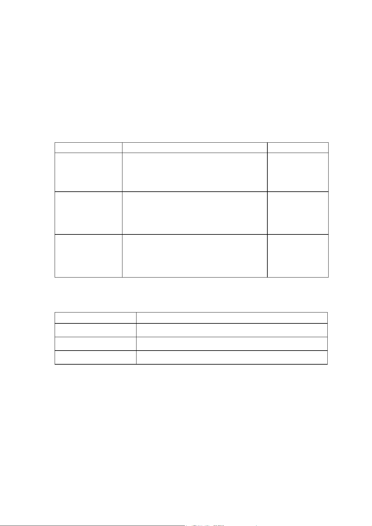
2. General Performance
2.1 Product Name
G5500/7050: Support GPRS (Class 10)
2.2 Supporting Standard
Item Feature Comment
E-GSM/ DCS Dual Band
Supporting Standard
Frequency Range
Application
Standard
with seamless handover
Phase 2+
SIM Toolkit : Class 1,2,3,A~E
E-GSM TX : 880 – 915 MHz
E-GSM RX : 925 – 960 MHz
DCS 1800 TX : 1710 – 1785 MHz
DCS 1800 RX : 1805 – 1880 MHz
WAP 2.0 : Yes
MMS : Yes
JAVA : MIDP v1.0.3
IrDA 1.3
2.3 Main Parts: GSM Solution
Digital Baseband CALYPSO @39MHz (D751992GHH)
Analog Baseband IOTA (TWL3014CGGM)
RF Chip Aero (Multi slot) (Si4200-BM, Si4201-BM, Si4133T-BM)
G5500/7050
-8-
2.4 H/W Features
Item Feature Comment
Form Factor Slide Down LCD (65K Color)
Battery
Capacity
Standard: Li-Ion, 860mAh
Cell Size: Standard
55(L)×33.7(W)×49.5(H)mm
Packing Type: Hard Pack
Size Standard: 94×44×21.5mm L×W×H
Weight 89g With Battery
PCB
AVG TCVR
current (mA)
Main PCB: 8Layers, 1t
Keypad PCB: 2Layers, 0.6t
Max : 260 mA (Power Level 5)
Max : 120 mA (Power Level 19)
Estimated
Standby Current 4.6mA @ Paging Period 9
Standby time
Charging time
Talk time
RX sensitivity
Up to 150 hours @ Paging Period 9
Below 3 hr. @ Power Off / 860mAh
Min : 4hr @Power Level 7
Min : 6hr @Power Level 12
@ 860mAh
GSM 900 : -105 dBm
DCS 1800 : -105 dBm
TX output power
GSM 900 : 32 dBm
DCS 1800 : 29 dBm
GPRS compatibility GPRS Class 10
SIM card type
Plug-In SIM - 3V
- LCD : 65K Color-STN (128 X160)
- Pixels : 0.219 x 0.219 mm
Display
- View Area : 30.54 x 36.04 mm
- Active Area : 28.02 x 35.028 mm
- Backlight : White LED
Status Indicator
Yes (Red, Green)
Alphanumeric Key : 12
Keypad
Function Key : 12
Side Key : 2
Total Number of Keys : 26
Class4 (GSM)
Class1 (DCS)
Function Key:
4 Key Navigation & OK,
F1, F2, SND, END/PWR,
Clear, Book Mark (Camera),
Voice Recording
-9-
Item Feature Comment
Antenna Fixed Type
System connector 24 Pin
Ear Phone Jack
PC synchronization
Memory Flash : 128Mbit / SRAM : 64Mbit AMD
Speech coding FR, EFR, HR
Data & Fax Built in Data & Fax support
Vibrator Built in Vibrator
IrDA Built in IrDA PC sync support
MIDI (for Buzzer
Function)
Voice Recording
Travel Adapter Yes
Camera Sensor
Options
3 Pole (φ2.5mm)
Yes
40 Poly
up to 90 sec 30sec x 3
VGA / CIS G7050 only
Travel Adapter
Ear-Microphone
Hand Strap
Cigarette Lighter Adapter
Data Cable
Handsfree Car Kit
Simple Hands Free kit
CDROM
Buzzer Function By Using
MIDI IC
TBD
TBD
-10-
2.5 S/W Features
Item Feature Comment
RSSI 0~5 level Antenna
Battery Charging 0~3 level
Key Volume 0~5 level
Keypad Volume 0~5 level
Effect sound volume 0~5 level
Ring Volume 1~5 level
Time/Date Display Yes
Text Input T9
Multi-language Yes
Quick Access Mode
PC Sync Schedule/Phonebook/SMS MS Scheduler & Outlook
Speed Dial
Profile
CLIP/CLR
Phonebook
Last Dial Number
Last Received
Number
Last Missed Number
Search Number/Name
Group
Fixed Dial Number
Voice Memo
Schedule/Ring Tone/Phonebook
Camera/GPRS/Phonebook(G7050)
Yes (2~9) Voice mail center → 1 key
Yes
Yes
3 Number + 1 Memo + 1 e-mail Phone (Up to 255 entries)
Yes (20)
Yes (20)
Yes (10)
Yes
7 / User Editor
Yes
30 secs * 3
Call Remainder
Network Selection
Yes
Automatic / Manual
-11-
Item Feature Comment
Mute Yes
Call Divert Yes
Call Barring Yes
Call Charge
Call Duration
SMS (EMS)
EMS
Send/Receive/Save
MMS
WAP Browser
Java
Wall Paper
Download Melody/
Wallpaper (MMS)
Long Message
Cell Broadcast
Calendar
Memo
Yes
Yes
100
Yes
Yes
WAP 2.0
CLDC v1.0.3 / MIDP v1.0.3
Yes Max. 10 preset
Over the WAP
Mac. 918 Character(6page*153)
Yes
Yes
20
Melody/Picture/Animation
World Clock
Unit Convert
Fax & Data
SIM Lock
SIM Toolkit
Camera
Phone lock/Key lock
Security
CPHS
IM
Yes
Length/Surface/Volume/Weight
Yes
Yes Operator Dependent
Class 1,2,3
Image resolution : 640 x 480
300 KB dynamic memory for
images : Max 100 photos (128 x 96)
Max 4x zoom
Yes
DRM (Forward-lock only)
Yes
Yes G7050 for T-Mobile only
G7050 only
-12-
3. H/W Circuit Description
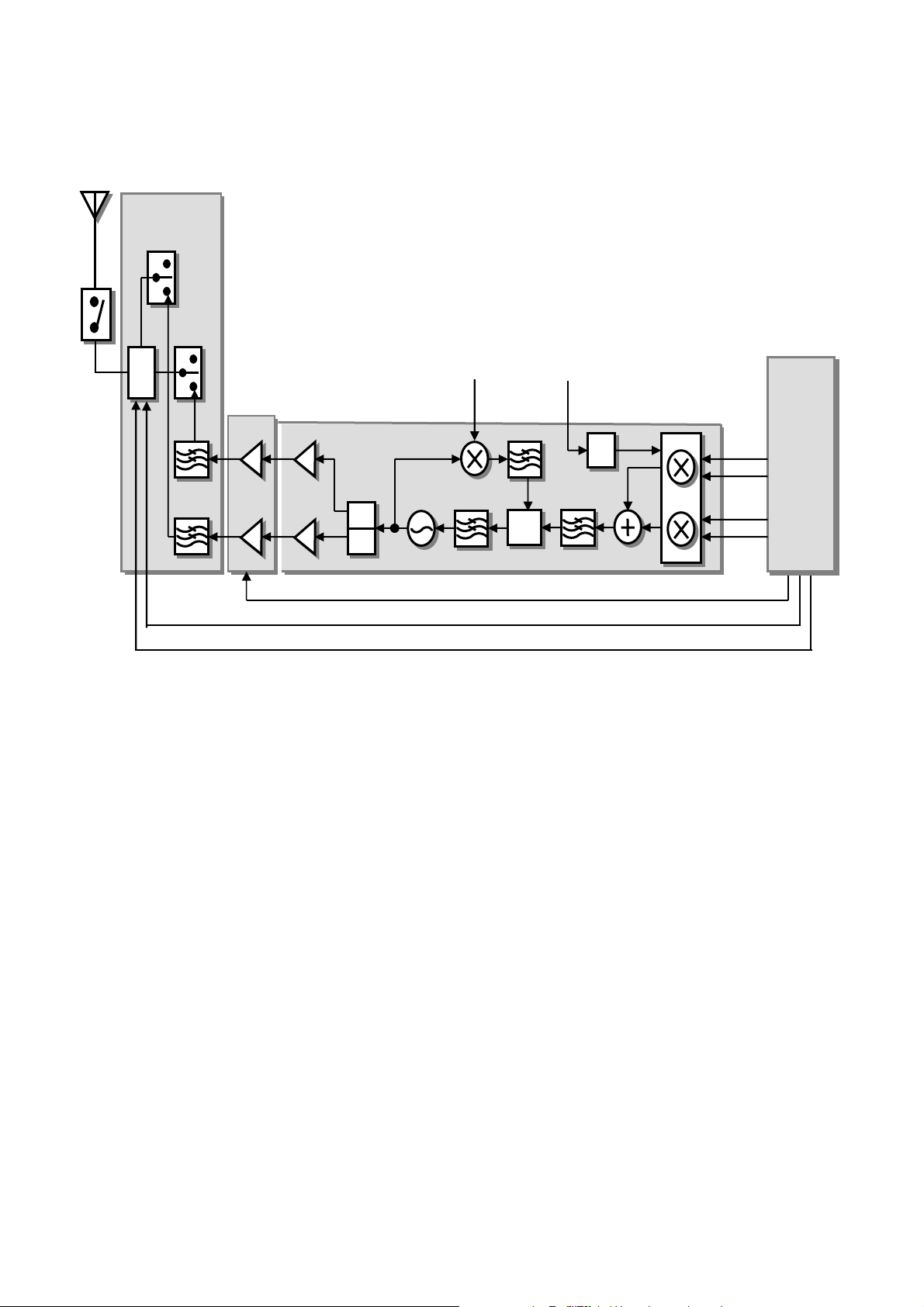
3.1 RF Transceiver General Description
The RF parts consist of a transmitter part, a receiver part, a frequency synthesizer part, a voltage
supply part, and a VC-TCXO part.
The Aero transceiver is composed of three RF chipsets, Si4200-BM[U502], Si4133T-BM[U505] and
Si4201-BM[U503] which is a dual and triple-band GSM/GPRS wireless communications.
This device integrated a receiver based on a low IF (100KHz) architecture and a transmitter based on
modulation loop architecture. And, the synthesizer[U505] part employed the Silicon Labs Si4133T-BM,
a complete dual band synthesizer with built in VCOs.
The transceiver employed a 3 wire serial interface to allow an external system controller to write the
control registers for dividers, receive path gain, power down setting, and other controls.
3.2 Receiver Part
The receiver part uses a low-IF receiver architecture that allows for the on-chip integration of the
channel selection filters, eliminating the external RF image reject filters and the IF SAW filter
required in conventional super-heterodyne architecture. The Si4200-BM[U502] integrates three
differential input LNAs that are matched to the 200 Ohm balanced-output SAW filters through
external LC matching networks. A quadrature image-rejection mixer downconverts the RF signal
to a 100kHz intermediate frequency (IF) with the RFLO from the Si4133T-BM[U505]. The mixer
output is amplified with an analog programmable gain amplifier (PGA) and quadrature IF signal is
digitized with high resolution A/D converters (ADCs). The Si4201-BM[U503] downconverts the ADC
output to baseband with a digital 100kHz quadrature LO signal. Digital decimation and IIR filters
perform channel selection to remove blocking and reference interference signals. After channel
selection, the digital output is scaled with digital PGA, which is controlled with the DGAIN[5:0] bits
in register 05h.The amplified digital output signal go through with DACs that drive a differential
analog signal onto the RXIP,RXIN,RXQP and RXQN pins to interface to standard analog ADC
input baseband ICs.
Antenna Display
Antenna Bar Number
5 ≥ -85
4 ≥ -90
3 ≥ -95
2 ≥ -100
2 ≥ -105
1 < -105
-13-
Power (dBm)
Figure 1. RF Receiver Block
FL501
Antenna Switch
EGSM
DCS
D
D
I
I
P
P
FL502
FL503
PAM
U504
RF3133
LNA
EGSM
DCS
PCS
0˚/
0˚/
90˚
90˚
U502/Si4200 U503/Si4201
PGA PGA
ADC
ADC
ADC
ADC
÷2:GSM
÷2:GSM
÷1:DCS
÷1:DCS
RF1
100KHz
100KHz
U505/Si4133T
RF
RF
PLL
PLL
Channel Filter
Channel Filter
IF
IF
PLL
PLL
RF2 IF
DAC
DAC
13MHz
DAC
DAC
U506
VC-TCXO
I
Q
Baseband
Baseband
Calypso
Calypso
(CO35)
(CO35)
3.2.1. RF Front End
RF front end consists of Antenna Switch(FL501), dual band LNAs integrated in transceiver(U502).
The Received RF signals (EGSM 925MHz ~ 960MHz, DCS 1805MHz ~ 1880MHz) are fed into the
antenna or mobile switch. An antenna matching circuit is between the antenna and the mobile switch.
The Antenna Switch(FL501) is used for control the Rx and TX paths. And, the input signals VC1 and
VC2 of a FL501 are directly connected to baseband controller to switch either TX or RX path on. Ant
S/W module(FL501) is an antenna switch module for dual band phone. The logic and current is given
below Table 3-1.
(TI)
(TI)
U102
U102
IOTA
IOTA
+
+
U101
U101
Table 3-1. The Logic and Current
EGSM TX
DCS TX
EGSM/DCS RX
VC1
0 V
2.5~3.0 V
0 V
VC2
2.5~3.0 V
0 V
0 V
Current
10.0 mA max
10.0 mA max
< 0.1 mA
The receiver part uses a low-IF receiver architecture that allows for the on-chip integration of the
channel selection filters, eliminating the external RF image reject filters and the IF SAW filter required
in conventional super-heterodyne architecture. The Si4200-BM[U502] integrates three differential
input LNAs that are matched to the 200 ohm balanced-output SAW filters through external LC
matching networks.
-14-

3.2.2. IF
A quadrate image-rejection mixer downconverts the RF signal to a 100kHz intermediate frequency (IF)
with the RFLO from the Si4133T-BM[U505]. The RFLO frequency is between 1849.8 and 1918.8 MHz,
and is divided by two in the Si4200 for EGSM modes. The RFLO frequency is between 1804.9 and
1879.9 MHz, and is divided by one in the Si4200 for DCS modes. The mixer output is amplified with
an analog programmable gain amplifier (PGA), which is controlled with the AGAIN[2:0] bits in register
05h.
The quadrate IF signal is digitized with high resolution A/D converters (ADCs).
The Si4201-BM[U503] down-converts the ADC output to baseband with a digital 100kHz quadrate LO
signal. Digital decimation and IIR filters perform channel selection to remove blocking and reference
interference signals. The response of the IIR filter is programmable to a high selectivity
setting(CSEL=0) or a low selectivity setting (CSEL=1). After channel selection, the digital output is
scaled with digital PGA, which is controlled with the DGAIN[5:0] bits in register 05h.
3.2.3. Demodulator and Baseband Processing
The amplified digital output signal go through with DACs that drive a differential analog signal onto the
RXIP, RXIN, RXQP and RXQN pins to interface to standard analog ADC input baseband ICs.
No special processing is required in the baseband for offset compensation or extended dynamic range.
Compared to a direct-conversion architecture, the low-IF architecture has a much greater degree of
immunity to dc offsets that can arise from RF local oscillator(RFLO) self-mixing, 2nd order distortion of
blockers, and device 1/f noise.
3.2.4. Synthesizer Part
The synthesizer IC, the Si4133T-BM[U505] is a monolithic CMOS integrated circuit that performs IF
and RF synthesis. Two complete PLLs are integrated including VCOs, varactors, resonators, loop
filters, reference and VCO dividers, and phase detectors. Differential outputs for the IF and RF PLLs
are provided for direct connection to the Si4200-BM[U502] transceiver IC. The RF PLL uses two
multiplexed VCOs.
The RF1 VCO is used for Receive mode, and the RF2 VCO is used for Transmit mode. The IF PLL is
used only during Transmit mode and uses a single VCO. The center frequency of each of the three
VCOs on the Si4133T is set by connection of an external inductance(Lext). The IF and RF output
frequencies are set by programming the N-Divider registers, N[RF1], N[RF2] and N[IF]. Programming
the N-Divider register for either RF1 or RF2 automatically selects the proper VCO. The output
frequency of each PLL is as follows:
fout = N * fø
A programmable divider at the XIN pin allows either a 13 or 26MHz from the external applied crystal
oscillator. The RF PLL phase detector update rate(fø) can be programmed with the RFUP bit in
register 31h to either fø = 100kHz or fø= 200kHz. The IF PLL always uses fø = 200kHz. Receive
mode should use fø = 100kHz in DCS1800 and PCS1900 bands, and fø = 200kHz in the GSM850 and
E-GSM 900 bands.
-15-
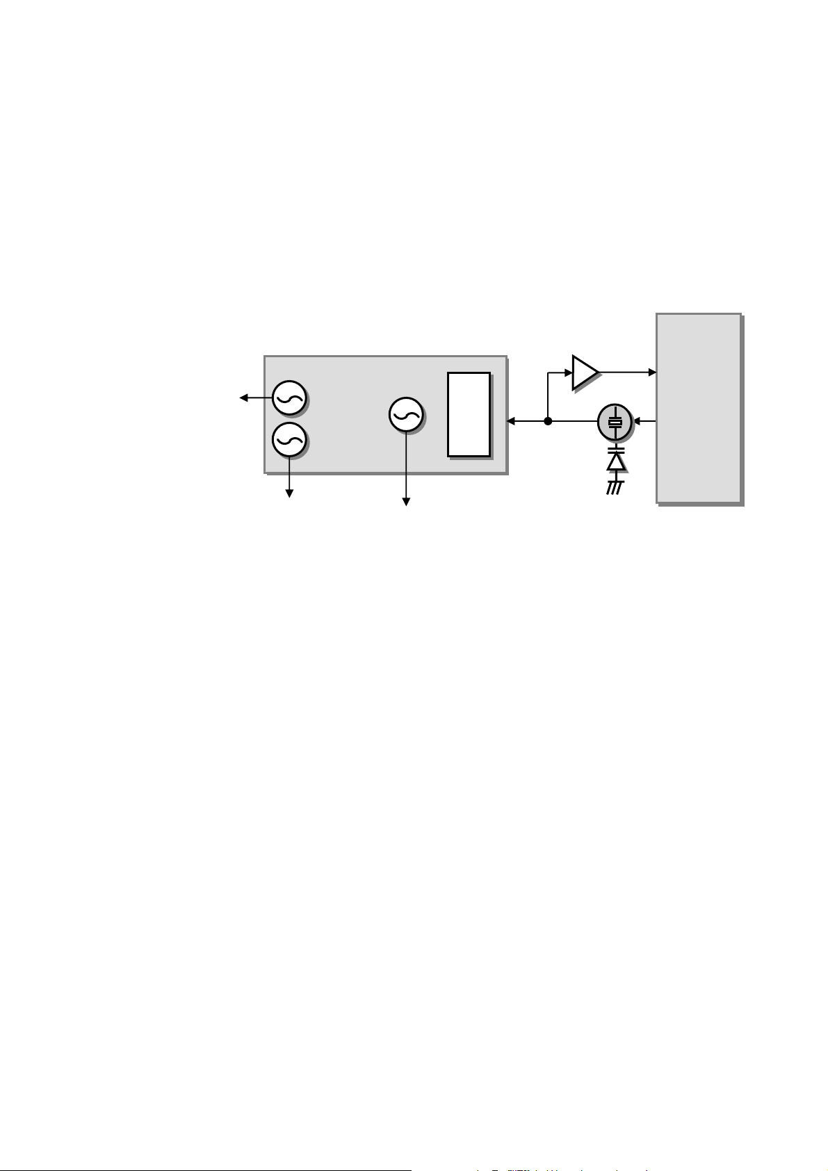
Transmit modes should always use fø = 200kHz. The IF and RF output frequencies are set by
programming the N-Divider registers and also programmed via 3-wire interface with external system
controller.
Figure 2. Synthesizer Block
Baseband
Baseband
(TI)
(TI)
U102
U102
IOTA
IOTA
+
+
U101
U101
Calypso
Calypso
(CO35)
(CO35)
RF_Lo(Rx)
U505/Si4133T
RF1
RF2 IF
IF
IF
PLL
PLL
U506
VC-TCXO
13MHz
RF_Lo(Tx)
IF_Lo(Tx)
3.2.5. Transmitter Part
The Transmitter part contains Si4200-BM[U502] active parts, Power Amp Module[U504] and Antenna
switch[FL501].
The transmit section of Si4200-BM [U502] consists of an I/Q baseband upconverter, an offset phaselocked loop (OPLL) and two 50 ohm output buffers that can drive external power amplifiers.
The RF GMSK outputs from the transmit VCO are fed directly to the RF power amplifiers.
The peak output power and the profile of the transmitted burst are controlled by means of incorporated
power control circuits inside of PA and DAC output. from the Baseband Controller. The PA outputs
pass to the antenna connector via Antenna Switch.
-16-
FL501
Antenna Switch
D
D
I
I
P
P
PAM
U504
RF3133
DCS
EGSM
Figure 3. RF Transmit Block
RF_Lo(Tx) IF_Lo(Tx)
÷1
÷1
÷2
÷2
PA_BAND
GATE_VC1
GATE_VC2
Φ
Φ
DET
DET
÷2
÷2
Q
I
Baseband
Baseband
(TI)
(TI)
U102
U102
IOTA
IOTA
+
+
U101
U101
Calypso
Calypso
(CO35)
(CO35)
3.2.6. IF Modulator
The baseband converter(BBC) within the GSM chipset generates I and Q baseband signals for the
Transmit vector modulator. The modulator provides more than 40dBc of carrier and unwanted sideband. Rejection and produces a GMSK modulated signal. The baseband software is able to cancel out
differential DC offsets in the I/Q baseband signals caused by imperfections in the D/A converters.
The TX-Modulator implements a quadrature modulator. A quadrature mixer upconverts the differential
I/Q signals with the IFLO to generate a SSB IF signal, which is filtered and used as the reference input
to the OPLL. The Si4133T[U706] generates the IFLO frequency. The IFLO is divided by two to
generate the quadrature LO signals for the quadrature modulator.
3.2.7. OPLL
The OPLL consists of a feedback mixer, a phase detector, a loop filter, and a fully integrated TXVCO.
The TXVCO is centered between the DCS 1800 and PCS 1900 bands, and its output is divided by 2
for the GSM 850 and E-GSM 900 bands. The Si4133T generates the RFLO frequency between 1327
and 1402 MHz. To allow a single VCO to be used for the RFLO, high-side injection is used for the
GSM 850 and E-GSM 900 bands, and low-side injection is used for the DCS 1800 and PCS 1900
bands. Low-pass filters before the OPLL phase detector reduce the harmonic content of the quadrature
modulator and feedback mixer outputs. The cutoff frequency of the filters is programmable with the
FIF[3:0] bits in register 04h. The OPLL requires no external duplexer to attenuate transmitter noise
and spurious signals in the receive band. Additionally, the output of the transmit VCO (TXVCO) is a
constant-envelope signal which reduces the problem of spectral spreading caused by non-linearity in
the PA.
-17-
3.2.8. Power Amplifier
The RF3133 [U504] is a triple-band GSM/DCS/PCS power amplifier module that incorporates an
indirect closed loop method of power control. The indirect closed loop is fully self-contained and it
does not require loop optimization. It can be driven directly from the DAC output in the baseband
circuit. On-board power control provides over 37 dB of control range with an analog voltage input
(Vramp). Efficiency is 55% at GSM and 52% at DCS.
Figure 4. Power Amp
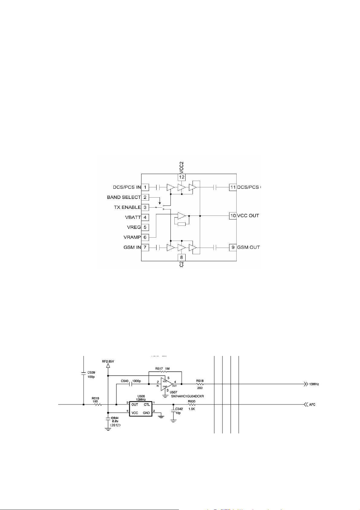
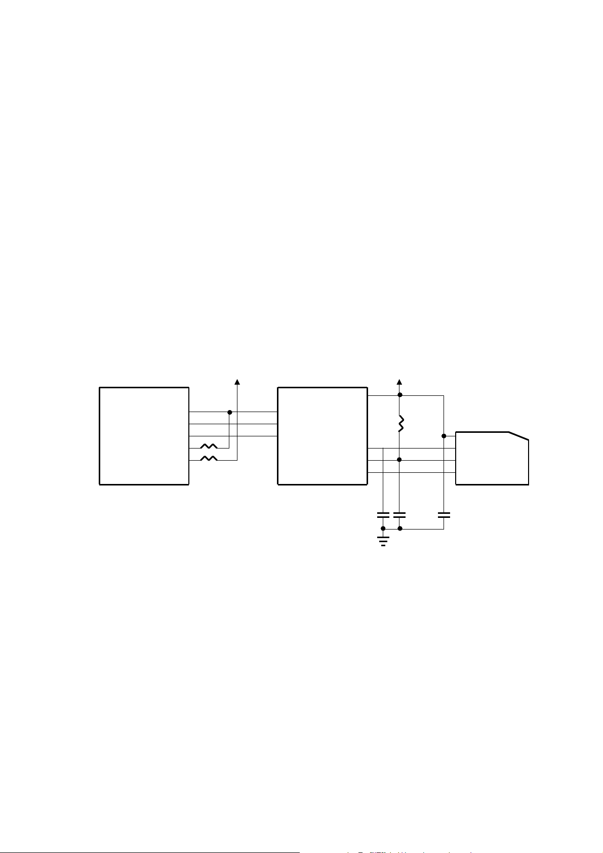
3.2.9. 13MHz Clock
The 13 MHz clock(U506) consists of a TCXO(Temperature Compensated Crystal Oscillator) which
oscillates at a frequency of 13 MHz. It is used within the Si4133T/Si4201 RF Main Chip, BB Analog
chip-set(IOTA), Digital chip-set(Calypso G2).
Figure 5. VC-TCXO Circuit
-18-
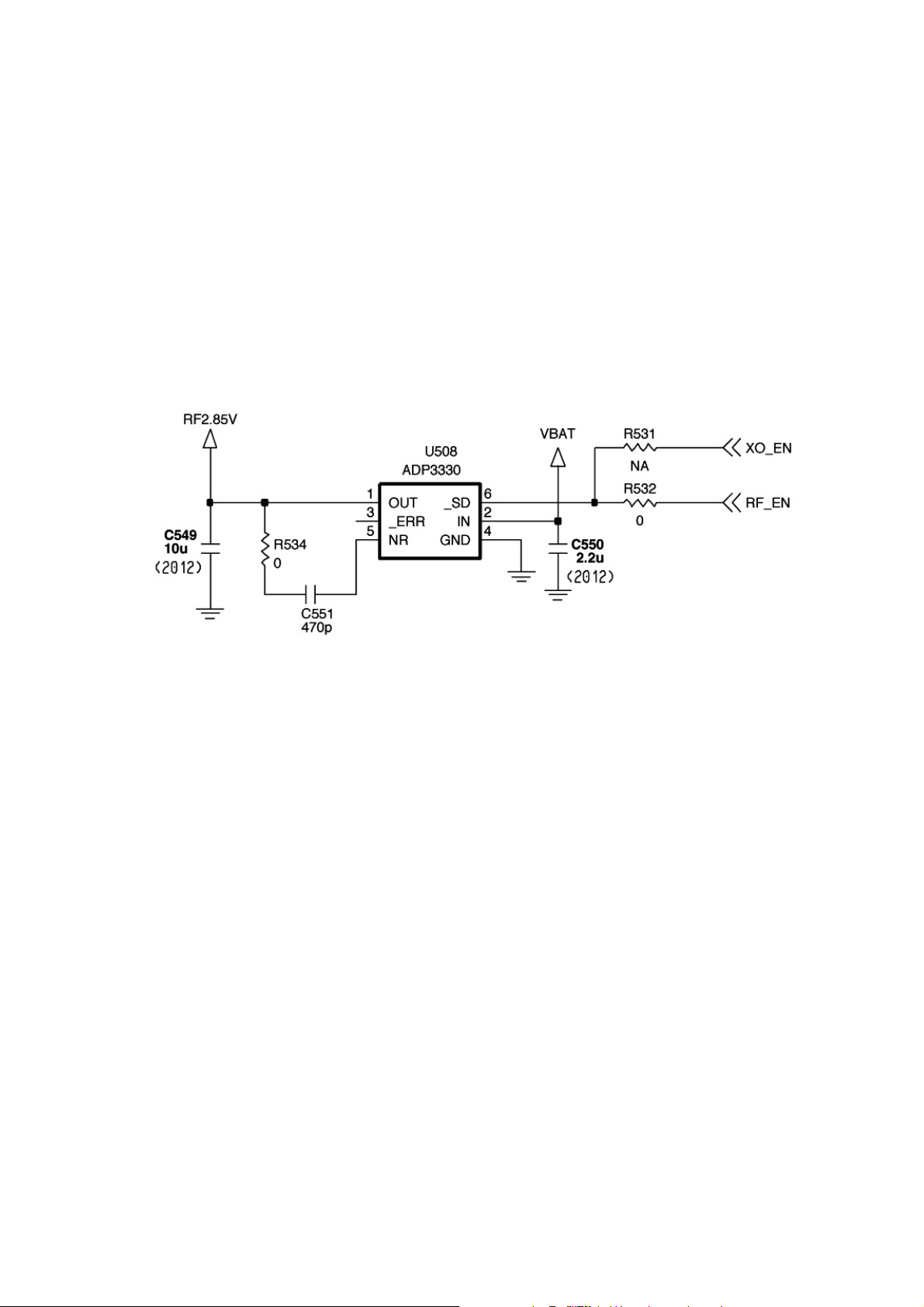
3.2.10. Power Supplies and Control Signals
An external regulator(U508) is used to provide DC power to RF part. Every RF component except
power amp module uses this external regulator.
Figure 6 External regulator Circuit
-19-
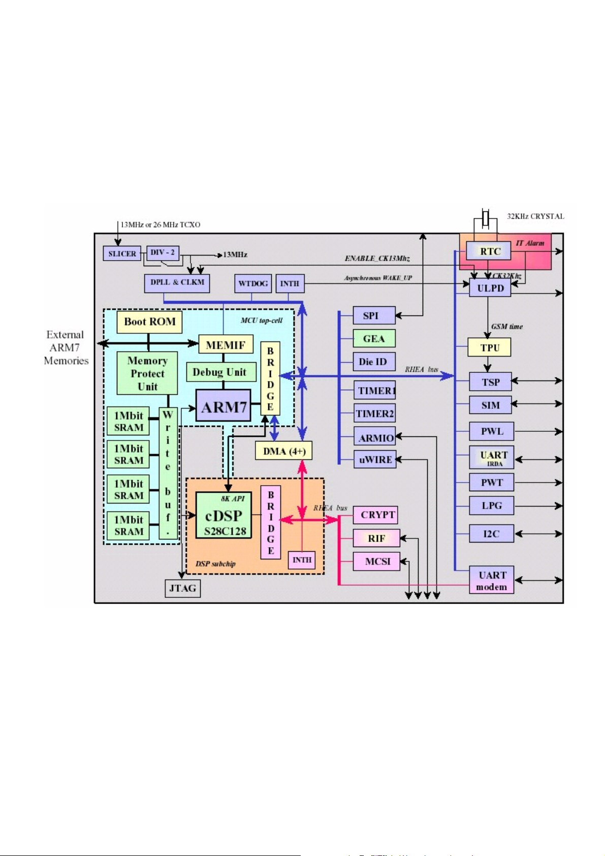
3.3 Digital Baseband (DBB) Processor
Figure 7. Top level block diagram of the Calypso G2(HERCROM400G2)
3.3.1. General Description
CALYPSO is a chip implementing the digital base-band processes of a GSM/GPRS mobile phone.
This chip combines a DSP sub-chip (LEAD2 CPU) with its program and data memories, a Micro- Controller core with emulation facilities (ARM7TDMIE), internal 8Kb of Boot ROM memory, 4M bit
SRAM memory, a clock squarer cell, several compiled single-port or 2-ports RAM and CMOS gates.
The chip will fully support the Full-Rate, Enhanced Full-Rate and Half-Rate speech coding.
CALYPSO implements all features for the structural test of the logic (full-SCAN, BIST, PMT, JTAG
boundary-SCAN).
-20-

3.3.2. Block Description
CALYPSO architecture is based on two processor cores ARM7 and DSP using the generic RHEA bus
standard as interface with their associated application peripherals.
CALYPSO is composed from the following blocks:
• ARM7TDMIE : ARM7TDMI CPU core
• DSP subchip
• ARM peripherals:
General purpose peripherals
• ARM Memory Interface for external RAM, Flash or ROM
• 4 Mbit Static RAM with write-buffer
Application peripherals
• ARM General purposes I/O with keyboard interface and two PWM modulation signals
• UART 16C750 interface (UART_IRDA) with
→ IRDA control capabilities (SIR)
→ Software flow control (UART mode).
• UART 16C750 interface (UART_MODEM) with
→ Hardware flow protocol (DCD, CTS/RTS)
→ Autobaud function
• SIM Interface.
• TPU(Time Processing Unit) : Processing for GSM time base
• TSP(Time Serial Port) : GSM data interface with RF and ABB
Memory Interface : External/Internal Memory Interface
nCS0 : FLASH1, 16bit access, 3 wait state
nCS1 : FLAHS2, 16bit access, 3 wait state
nCS2 : Ext SRAM, 16bit access, 3 wait state
nCS3 : Main LCD(16bit access), OEL(8bit access) addressing, 3 wait state
nCS4 : MIDI(8bit access), USB(8bit access) addressing, 3 wait state
nCS6 : Int SRAM, 32bit access, 0 wait state
* Calypso is internally 39MHz machine (25ns machine cycle), so it requires 3 wait-state for 80ns
access(25*4 = 100 ns).
-21-
3.3.3. External Devices connected to memory interface
Table 3-2. Memory interface
Device Name Maker
FLASH1 AM50DL128CG70I AMD 70ns 70ns
FLASH2 AM50DL128CG70I AMD 70ns 70ns
SRAM AM50DL128CG70I AMD 70ns 70ns
LCD S6B33B0A SDI 50ns 50ns
Melody IC YMU762 Yamaha 50ns 80ns
Write
Access Time
Read
Access Time
3.3.4. RF Interface (TPU, TSP Block)
Calypso uses this interface to control IOTA_CS(ABB Processor) and AERO(RF Processor) with GSM
Time Base
Table 3-3. RF Interface Spec.
TSP (Time Serial Port)
Resource Interconnection Description
TSPDO ABB & RF main Chip Control Data
TSPEN0 ABB ABB Control Data Enable Signal
TSPEN1 RF main Chip RF Control Data Enable Signal
TSP (Time Serial Port)
TSPACT00 PDNB RF main Chip Reset Signal
TSPACT01 PA_ON Power Amp ON signal
-22-
3.3.5. SIM Interface
SIM interface scheme is shown in (Figure 8).
SIM_IO, SIM_CLK, SIM_RST ports are used to communicate DBB with ABB and the Charge Pump in
ABB enables 1.8V/3V SIM operation.
SIM Interface
SIM_CLK SIM card reference clock
SIM_RST SIM card async/sync reset
SIM_IO SIM card bidirectional data line
SIM_PWCTRL SIM card power activation
SIM_CD SIM card presence detection
Figure 8. SIM Interface
DBB ABB
DBB ABB
SIM_IO
SIM_IO
SIM_CLK
SIM_CLK
SIM_RST
SIM_RST
SIM_PWRCTRL
SIM_PWRCTRL
SIM_CD
SIM_CD
10k
10k
V_IO
V_IO
DBBSIO
DBBSIO
DBBSCK
DBBSCK
DBBSRST
DBBSRST
3.3.6. UART Interface
G5500/7050 has two UART Drivers as follow :
UART1 : Hardware Flow Control / Fax & Data Modem
UART2 : Handsfree Control / SW trace or IrDA Modem
VRSIM
VRSIM
SIMCLK
SIMCLK
SIMIO
SIMIO
SIMRST
SIMRST
150p 22p
150p 22p
V_SIM
V_SIM
10k
10k
1u
1u
VPP
VPP
CLK
CLK
IO
IO
RST
RST
SIM
SIM
-23-
Figure 3-4. UART Interface spec.
UART MODEM (UART1)
Resource Name Description
TX_MODEM TXD Transmit Data
RX_MODEM RXD Receive Data
CTS_MODEM CTS Clear To Send
RTS_MODEM RTS Request To Send
GPIO 3 DSR Data Set Ready
UART IrDA (UART2)
Resource Name Description
TXIR_IRDA TX_IRDA Infra-Red Transmit Pulse
TX_IRDA TX Transmit Data(UART2)
RXIR_IRDA RX_IRDA Infra-Red Receive Pulse
RX_IRDA RX Receive Data(UART2)
SD_IRDA SD_IRDA IRDA transceiver Shutdown Mode
-24-

3.3.7. GPIO Map
In total 16 allowable resources, G5500/7050 is using 13 resources except 3 resources dedicated to
SIM and Memory. G5500/7050 GPIO (General Purpose Input/Output) Map, describing application, I/O
state, and enable level, is shown in below table.
Table 5. GPIO Map Table
I/O # Application I/O
I/O (0) FLIP I GPIO HIGH (Open) LOW (Closed)
I/O (1) MIDI_INT I GPIO HIGH LOW
I/O (2) CAM_INT I GPIO HIGH LOW
I/O (3) DSR I GPIO HIGH LOW
I/O (4) LCD_ID I GPIO LOW HIGH
I/O (5) SIM_PWRCTRL O SIM HIGH HIGH
I/O (6) JACK_DETECT I GPIO LOW HIGH
I/O (7) LCD_RESET O GPIO HIGH LOW
I/O (8) SPK_EN O GPIO LOW(REC) HIGH(SPK)
I/O (9) CAM_HOLD O GPIO LOW HIGH
I/O (10) INDLED_R O GPIO LOW HIGH
I/O (11) INDLED_G O GPIO LOW HIGH
I/O (12) STROBE O GPIO RESERVED
I/O (13) HANDSFREE I GPIO HIGH LOW
I/O (14) NBHE O MEMORY
I/O (15) NBLE O MEMORY
Resource
State
Inactive
State
Active
State
3.4 Analog Baseband (ABB) Processor
3.4.1. General Description
IOTA is Analog Baseband (ABB) Chip supports GSM900, DCS1800, PCS1900, GPRS Class 10 with
Digital Basband Chip (Calypso G2).
IOTA processes GSM modulation/demodulation and power management operations.
Block Description
• Audio Signal Processing & Interface
• Baseband in-phase(I), quadrature(Q) Signal Processing
• RF interface with DBB (time serial port)
• Supply voltage regulation
-25-

• Battery charging control
• Switch ON/OFF
• 1.8V/3V SIM card Interface
• 4 internal & 4external ADC channels
Figure 9. Top level block diagram of the IOTA(TWL3014CGGM)
-26-
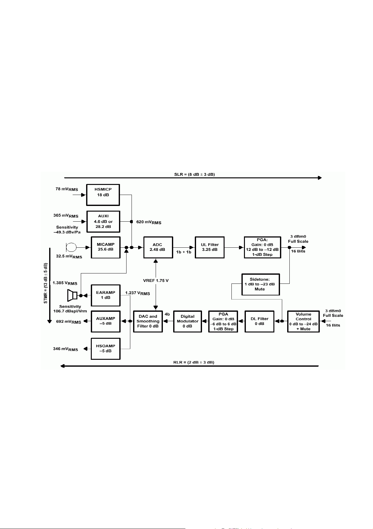
3.4.2. Audio Signal Processing & Interface
The voice codec circuitry processes analog audio components in the voice uplink (VUL) path and
applies this signal to the voice signal interface for eventual baseband modulation. In the voice
downlink (VDL) path, the codec circuitry changes voice component data received from the voice serial
interface (VSP) into analog audio.
Figure 10. Audio Interface Block Diagram
-27-
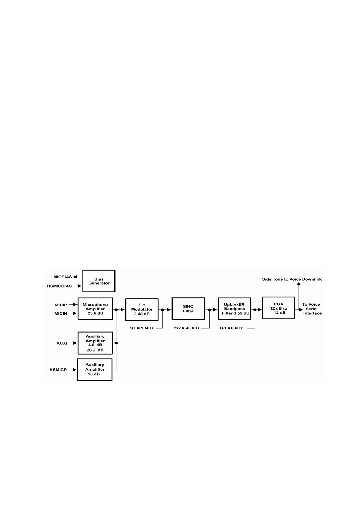
3.4.3. Audio uplink processing
The VUL path includes two input stages. The first stage is a microphone amplifier, compatible with
electret microphones containing a FET buffer with open drain output. The microphone amplifier has a
gain of typically 25.6 dB (±1 dB) and provides an external voltage of 2.0 V or 2.5 V to bias the
microphone (MICBIAS). The auxiliary audio input can be used as an alternative source for higher level
speech signals. This stage performs single-ended-to differential conversion and provides a
programmable gain of 4.6 dB or 28.2 dB. The third stage is a headset microphone amplifier,
compatible with electret microphones. The headset microphone amplifier has a gain of typically 18 dB
and provides an external voltage of 2.0 V or 2.5 V to bias the headset microphone (HSMICBIAS).
When one of the input stages (MICI, AUXI, HSMICP) is in use, the two other input stages are disabled
and powered down. The resulting fully differential signal is fed to the analog-to-digital converter (ADC).
The ADC conversion slope depends on the value of the internal voltage reference. Analog-to-digital
conversion is performed by a third-order Σ-Δ modulator with a sampling rate of 1 MHz. Output of the
ADC is fed to a speech digital filter, which performs the decimation down to 8 kHz and band-limits the
signal with both low-pass and high-pass transfer functions. Programmable gain can be set digitally
from -12 dB to +12 dB in 1-dB steps and is programmed with bits 4-0 (VULPG(4:0)) of the voiceband
uplink register. The speech samples are then transmitted to the DSP via the VSP at a rate of 8 kHz.
There are 15 meaningful output bits. Programmable functions of the VUL path, power-up, input
selection, and gain are controlled by the BSP or the USP via the serial interfaces.
The VUL path can be powered down by bit 0 (VULON) of the power down register.
Figure 11. Uplink Path
-28-
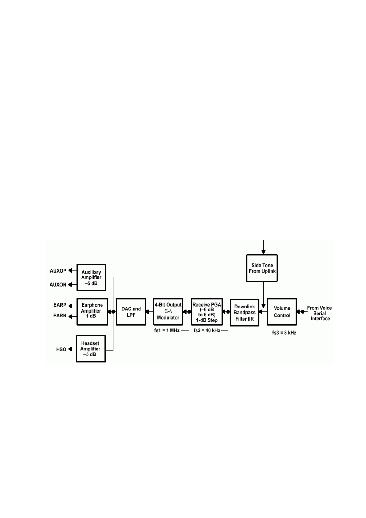
3.4.4. Audio downlink processing
The VDL path receives speech samples at the rate of 8 kHz from the DSP via the VSP and converts
them to analog signals to drive the external speech transducer. The digital speech coming from the
DSP is first fed to a speech digital filter that has two functions. The first function is to interpolate the
input signal and to increase the sampling rate from 8 kHz up to 40 kHz to allow the digital-to-analog
conversion to be performed by an oversampling digital modulator. The second function is to band-limit
the speech signal with both low-pass and high-pass transfer functions. The filter, the PGA gain, and
the volume gain can be bypassed by programming bit 9 (VFBYP) in the voiceband control register 1.
The interpolated and band-limited signal is fed to a second order Σ-Δ digital modulator sampled at 1
MHz to generate a 4-bit (9 levels) oversampled signal. This signal is then passed through a dynamic
element matching block and then to a 4-bit digital-to-analog converter (DAC). The volume control and
the programmable gain are performed in the voiceband digital filter. Volume control is performed in
steps of 6 dB from 0 dB to -24 dB. In mute state, attenuation is higher than 40 dB. A fine adjustment of
gain is possible from -6 dB to +6 dB in 1-dB steps to calibrate the system depending on the earphone
characteristics. This configuration is programmed with the voiceband downlink control register.
Figure 12. Downlink Path
-29-
3.4.5. Baseband Codec (BBC)
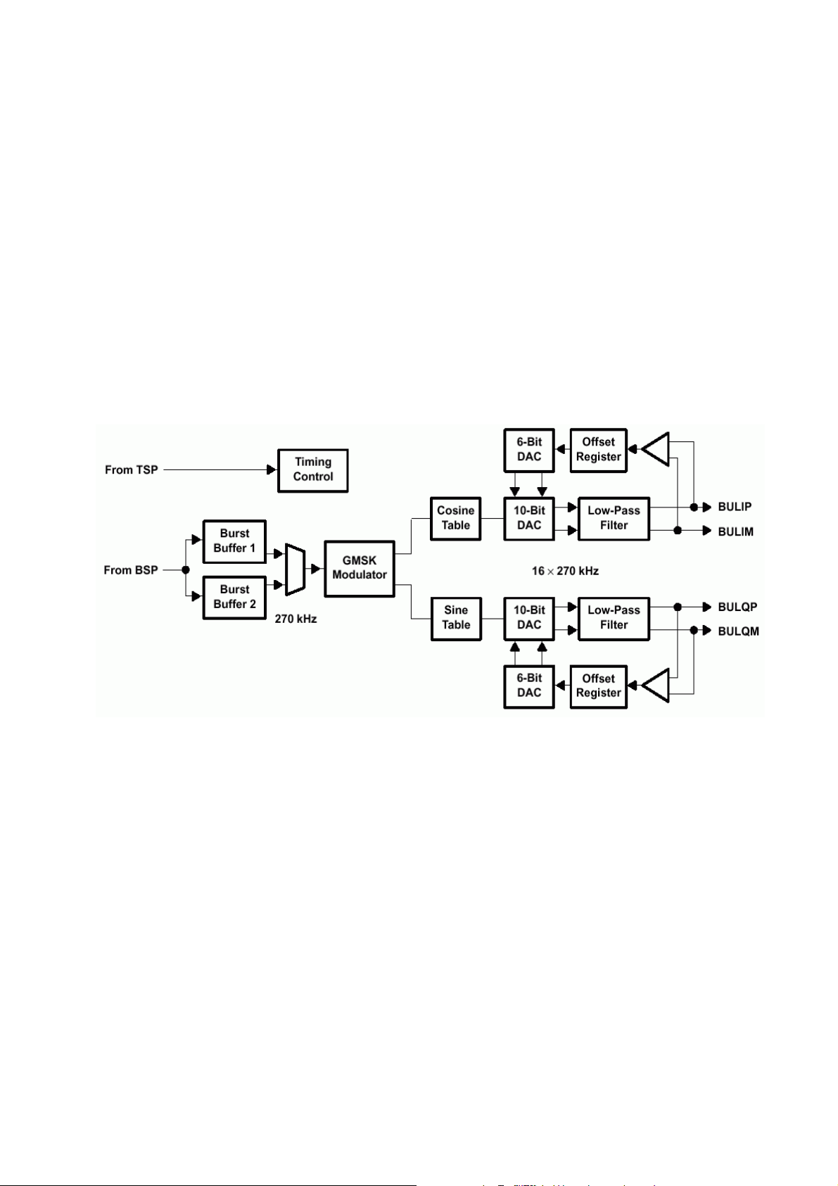
Baseband codec is composed of baseband uplink path (BUL) and baseband downlink path (BDL).
BUL makes GMSK (Gaussian Minimum Shift Keying) modulated signal which has In-phase (I)
component and quadrature (Q) component with burst data from DBB. This modulated signal is
transmitted through RF section via air.
BDL process is opposite procedure of BUL. Namely, it performs GMSK demodulation with input
analog I&Q signal from RF section, and then transmit it to DSP of DBB chip with 270.833kHz data rate
through BSP.
Figure 13. Baseband Codec Block Diagram
3.4.6. Voltage Regulation (VREG)
There are 7 LDO (Low Drop Output) regulators in ABB chip.
The output of these 7 LDOs are as following table. (Figure14) shows the power supply related blocks
of DBB/ABB and their interfaces in G5500/7050.
-30-
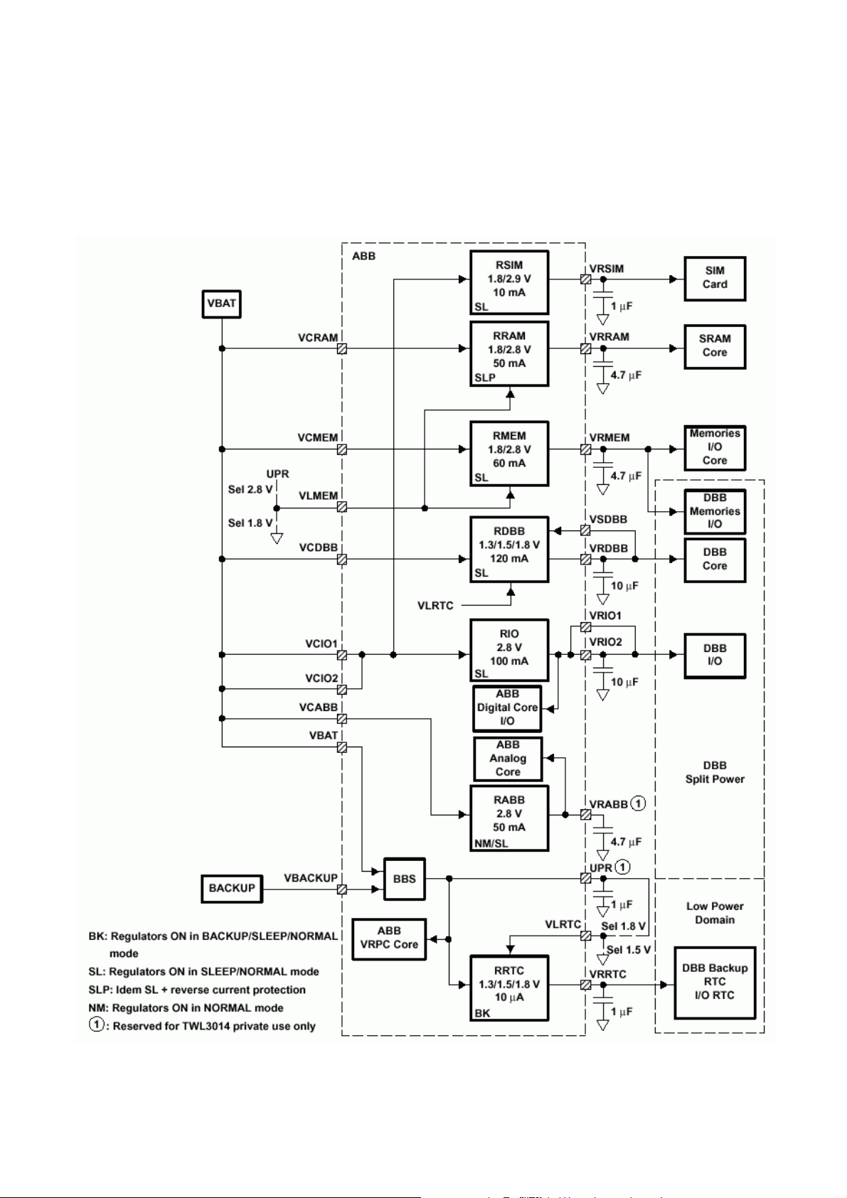
Figure 14. Power Supply Scheme
-31-
 Loading...