

LG G5400 Service Manual

Service Manual
Service Manual
G5400
Model : G5400
P/N : MMBD0022701 Date: May, 2003

- 3 -
Table Of Contents
1. INTRODUCTION
..................................
5
1.1 Purpose
.................................................
5
1.2 Regulatory Information
..........................
5
A. Security
.............................................
5
B. Incidence of Harm
.............................
5
C. Changes in Service
...........................
5
D. Maintenance Limitations
...................
5
E. Notice of Radiated Emissions
............
6
F. Pictures
.............................................
6
G. Interference and Attenuation
............
6
H. Electrostatic Sensitive Devices
.........
6
1.3 Abbreviations
.........................................
7
2. PERFORMANCE
....................................
8
2.1 H/W Feature
..........................................
8
2.2 Technical Specification
..........................
9
3. TECHNICAL BRIEF
............................
13
3.1 General Description
.............................
13
3.2 Receiver Part
.......................................
13
A. RF front end
....................................
13
B. IF
.....................................................
13
C. Demodulator and base processing..14
3.3 Synthesizer Part
..................................
14
3.4 Transmitter Part
...................................
15
A. IF Modulator
....................................
16
B. OPLL
...............................................
16
C. Power Amplifier
................................
16
3.5 13MHz Clock
.......................................
17
3.6 Power Supplies and Control Signals
...
17
3.7 Digital Main Processor
.........................
18
3.8 Analog Main Processor
........................
21
3.9 Power management IC
........................
27
3.10 Memories
...........................................
27
3.11 Display and Interface
.........................
27
3.12 Keypad Switches and Scanning
........
27
3.13 Microphone
........................................
29
3.14 Earpiece
.............................................
30
3.15 Hands-free Interface
..........................
30
3.16 Headset Jack Interface
......................
30
3.17 Key Back-light Illumination
.................
31
3.18 LCD Back-light Illumination
................
31
3.19 Speaker & MIDI IC
..............................
32
4. TROUBLE SHOOTING
.....................
33
4.1 RF Components
.................................
33
4.2 RX Trouble
.........................................
34
4.2.1 Checking Regulator Circuit
........
35
4.2.2 Checking VCTCXO Circuit
........
36
4.2.3 Checking PLL Control Signal
.....
37
4.2.4 Checking Ant SW & Mobile SW..38
4.2.5 Checking SAW Filter Circuit
.......
39
4.2.6 Checking RX IQ
.........................
40
4.3 Tx Trouble
..........................................
41
4.3.1 Checking Regulator Circuit
........
42
4.3.2 Checking VCTCXO Circuit
........
43
4.3.3 Checking PLL Control Signal
.....
44
4.3.4 Checking Ant SW & Mobile SW..45
4.3.5 Checking SAW Filter Circuit
........
46
4.3.6 Checking TX IQ
.........................
47
4.3.7 Receiver and Transmitter
RF Level
....................................
48
4.4 Power On Trouble
..............................
49
4.5 Charging Trouble
...............................
51
4.6 LCD Trouble
.......................................
53
4.7 Receiver Trouble
................................
55
4.8 Speaker Trouble
.................................
57
4.9 MIC Trouble
.......................................
59
4.10 Vibrator Trouble
...............................
61
4.11 Key Backlight LED Trouble
..............
63
4.12 Folder on/off Trouble
........................
65
4.13 SIM Detect Trouble
..........................
67
4.14 Earphone Trouble
............................
69
4.15 HFK Trouble
.....................................
73
5. DISASSEMBLY
INSTRUCTION
.....................................
77
5.1 Disassembly
.......................................
77

- 4 -
6. DOWNLOAD AND
CALIBRATION
.....................................
84
6.1 Download
............................................
84
A. Download Setup
...............................
84
B. Download Procedure
.......................
85
6.2 Calibration
..........................................
91
A. Equipment List
................................
91
B. Equipment Setup
.............................
91
C. Test Jig Operation
...........................
92
7. BLOCK DIAGRAM
...............................
94
8. CIRCUIT DIAGRAM
.............................
95
8.1 MAIN
..................................................
95
8.2 AUDIO
................................................
96
8.3 MIDI
....................................................
97
8.4 RF CIRCUIT
.......................................
98
8.5 Keypad
...............................................
99
8.6 SIM, IrDA, Battery
............................
100
9. PCB LAYOUT
.....................................
100
10. ENGINEERING MODE
..................
103
A. About Engineering Mode
...............
103
B. Access Codes
...............................
103
C. Key Operation
...............................
103
10.1 BB Test [MENU 1]
........................
103
A. LCD [1-1]
.......................................
103
B. LCD [1-2]
.......................................
103
C. Backlight [1-3]
...............................
103
D. Buzzer [1-4]
...................................
103
E. Vibrator [1-45]
...............................
103
F. ADC (Analog to Digital
Converter) [1-6]
..............................
103
G. BATTERY [1-7]
.............................
103
H. Audio [1-8]
.....................................
103
I. DAI (Digital Audio Interface) [1-9]
...
103
10.2 RF Test [MENU 2]
........................
105
A. SAR Test [2-1]
...............................
105
10.3 MF Mode [MENU 3]
......................
105
A. All auto test [3-1]
...........................
105
B. LED [3-2]
.......................................
105
C. Backlight [3-3]
...............................
105
D. Buzzer [3-4]
...................................
105
E. Vibrator [3-5]
.................................
105
F. LCD [3-6]
.......................................
105
G. Keypad
..........................................
105
H. Sub LCD
.......................................
105
10.4 Trace option [MENU 4]
.................
106
10.5 Call Timer [MENU 5]
.....................
106
A. All calls [5-1]
..................................
106
B. Reset settings [5-2]
.......................
106
10.6 Fact. Reset [MENU 6]
...................
106
10.7 S/W version [MENU 7]
..................
106
11. STAND ALONE TEST
...................
107
11.1 Introduction
...................................
107
A. Tx Test
..........................................
107
B. Rx Test
..........................................
107
11.2 Setting Method
.............................
107
A. COM port
.......................................
107
B. Tx
..................................................
107
C. Rx
..................................................
107
11.3 Means of Test
...............................
108
12. AUTO CALIBRATION
...................
110
12.1 Overview
.......................................
110
12.2 Requirements
...............................
110
12.3 Menu and settings
........................
110
12.4 AGC
..............................................
112
12.5 APC
..............................................
112
12.6 ADC
..............................................
112
12.7 Setting
..........................................
112
12.8 How to do calibration
....................
112
13. EXPLODED VIEW &
REPLACEMENT PART LIST
......
113
13.1 Exploded View
..............................
113
13.2 Accessories
..................................
117
13.3 Replacement Part List
..................
118

1. INTRODUCTION
- 5 -
1. INTRODUCTION
1.1 Purpose
This manual provides the information necessary to repair, calibration, description and download the
features of this model.
1.2 Regulatory Information
A. Security
Toll fraud, the unauthorized use of telecommunications system by an unauthorized part (for
example, persons other than your company’s employees, agents, subcontractors, or person working
on your company’s behalf) can result in substantial additional charges for your telecommunications
services. System users are responsible for the security of own system. There are may be risks of
toll fraud associated with your telecommunications system. System users are responsible for
programming and configuring the equipment to prevent unauthorized use. The manufacturer does
not warrant that this product is immune from the above case but will prevent unauthorized use of
common-carrier telecommunication service of facilities accessed through or connected to it. The
manufacturer will not be responsible for any charges that result from such unauthorized use.
B. Incidence of Harm
If a telephone company determines that the equipment provided to customer is faulty and possibly
causing harm or interruption in service to the telephone network, it should disconnect telephone
service until repair can be done. A telephone company may temporarily disconnect service as long
as repair is not done.
C. Changes in Service
A local telephone company may make changes in its communications facilities or procedure. If
these changes could reasonably be expected to affect the use of the this phone or compatibility with
the network, the telephone company is required to give advanced written notice to the user, allowing
the user to take appropriate steps to maintain telephone service.
D. Maintenance Limitations
Maintenance limitations on this model must be performed only by the manufacturer or its authorized
agent. The user may not make any changes and/or repairs expect as specifically noted in this
manual. Therefore, note that unauthorized alternations or repair may affect the regulatory status of
the system and may void any remaining warranty.

1. INTRODUCTION
- 6 -
E. Notice of Radiated Emissions
This model complies with rules regarding radiation and radio frequency emission as defined by local
regulatory agencies. In accordance with these agencies, you may be required to provide information
such as the following to the end user.
F. Pictures
The pictures in this manual are for illustrative purposes only; your actual hardware may look slightly
different.
G. Interference and Attenuation
Phone may interfere with sensitive laboratory equipment, medical equipment, etc.Interference from
unsuppressed engines or electric motors may cause problems.
H. Electrostatic Sensitive Devices
ATTENTION
Boards, which contain Electrostatic Sensitive Device (ESD), are indicated by the sign.
Following information is ESD handling:
Service personnel should ground themselves by using a wrist strap when exchange system
boards.
When repairs are made to a system board, they should spread the floor with anti-static mat which
is also grounded.
Use a suitable, grounded soldering iron.
Keep sensitive parts in these protective packages until these are used.
When returning system boards or parts like EEPROM to the factory, use the protective package
as described.
1. INTRODUCTION
- 7 -
APC Automatic Power Control
BB Baseband
BER Bit Error Ratio
CC-CV Constant Current – Constant Voltage
DAC Digital to Analog Converter
DCS Digital Communication System
dBm dB relative to 1 milliwatt
DSP Digital Signal Processing
EEPROM Electrical Erasable Programmable Read-Only Memory
ESD Electrostatic Discharge
FPCB Flexible Printed Circuit Board
GMSK Gaussian Minimum Shift Keying
GPIB General Purpose Interface Bus
GSM Global System for Mobile Communications
IPUI International Portable User Identity
IF Intermediate Frequency
LCD Liquid Crystal Display
LDO Low Drop Output
LED Light Emitting Diode
OPLL Offset Phase Locked Loop
PAM Power Amplifier Module
PCB Printed Circuit Board
PGA Programmable Gain Amplifier
PLL Phase Locked Loop
PSTN Public Switched Telephone Network
RF Radio Frequency
RLR Receiving Loudness Rating
RMS Root Mean Square
RTC Real Time Clock
SAW Surface Acoustic Wave
SIM Subscriber Identity Module
SLR Sending Loudness Rating
SRAM Static Random Access Memory
PSRAM Paeudo SRAM
STMR Side Tone Masking Rating
TA Travel Adapter
TDD Time Division Duplex
TDMA Time Division Multiple Access
UART Universal Asynchronous Receiver/Transmitter
VCO Voltage Controlled Oscillator
VCTCXO Voltage Control Temperature Compensated Crystal Oscillator
WAP Wireless Application Protocol
1.3 Abbreviations
For the purposes of this manual, following abbreviations apply:

2. PERFORMANCE
- 8 -
Item Feature Comment
Li-ion, 740 mAh
Standard Battery Size: 34 X50 X4.5mm
Weight: 17.2g
Under the minimum current consumption environment
Stand by Current (such as paging period 9), the level of standby current is
below 4mA.
Talk time Up to 3 hours (GSM TX Level 7)
Stand by time Up to 200 hours (Paging Period: 9, RSSI: -85 dBm)
Charging time 2.3 hours
RX Sensitivity GSM, EGSM: -105dBm, DCS: -105dBm
TX output power
GSM, EGSM: 32 dBm (Level 5)
DCS: 29dBm (Level 0)
GPRS compatibility Class 10
SIM card type 3V Small
Display 128 X128 pixel 65K Color LCD
Hard icons
Key Pad:
Status Indicator
0 ~ 9, #, * , Up/Down Navigation Key
& keypad
Confirm Key, Clear Key
Send Key, END/PWR Key
ANT external
EAR Phone Jack Yes
PC Synchronization Yes
Speech coding EFR/FR/HR
Data and Fax Yes
Vibrator Yes
Loud Speaker Yes
Voice Recording Yes
C-Mike Yes
Receiver Yes
Travel Adapter Yes
Options Hands-free kit, CLA, Data Kit
2. PERFORMANCE
2.1 H/W Features
2. PERFORMANCE
- 9 -
Item Description Specification
GSM
TX: 890 + n X0.2 MHz
RX: 935 + n X0.2 MHz (n = 1 ~ 124)
EGSM
1 Frequency Band TX: 890 + (n – 1024) X0.2 MHz
RX: 935 + (n – 1024) X0.2 MHz (n = 975 ~ 1024)
DCS
TX: 1710 + (n – 512) X0.2 MHz
Rx: 1805 + (n – 512) X0.2 MHz (n = 512 ~ 885)
2 Phase Error
RMS < 5 degrees
Peak < 20 degrees
3 Frequency Error < 0.1 ppm
GSM, EGSM
Level Power Toler. Level Power Toler.
5 33 dBm ± 2dB 13 17 dBm ± 3dB
6 31 dBm ± 3dB 14 15 dBm ± 3dB
7 29 dBm ± 3dB 15 13 dBm ± 3dB
8 27 dBm ± 3dB 16 11 dBm ± 5dB
9 25 dBm ± 3dB 17 9 dBm ± 5dB
10 23 dBm ± 3dB 18 7 dBm ± 5dB
11 21 dBm ± 3dB 19 5 dBm ± 5dB
4 Power Level 12 19 dBm ± 3dB
DCS
Level Power Toler. Level Power Toler.
0 30 dBm ± 2dB 8 14 dBm ± 3dB
1 28 dBm ± 3dB 9 12 dBm ± 4dB
2 26 dBm ± 3dB 10 10 dBm ± 4dB
3 24 dBm ± 3dB 11 8 dBm ± 4dB
4 22 dBm ± 3dB 12 6 dBm ± 4dB
5 20 dBm ± 3dB 13 4 dBm ± 4dB
6 18 dBm ± 3dB 14 2 dBm ± 5dB
7 16 dBm ± 3dB 15 0 dBm ± 5dB
2.2 Technical Specification

2. PERFORMANCE
- 10 -
Item Description Specification
GSM, EGSM
Offset from Carrier (kHz). Max. dBc
100 +0.5
200 -30
250 -33
400 -60
600 ~ <1,200 -60
1,200 ~ <1,800 -60
1,800 ~ <3,000 -63
3,000 ~ <6,000 -65
5 Output RF Spectrum 6,000 -71
(due to modulation)
DCS
Offset from Carrier (kHz). Max. dBc
100 +0.5
200 -30
250 -33
400 -60
600 ~ <1,200 -60
1,200 ~ <1,800 -60
1,800 ~ <3,000 -65
3,000 ~ <6,000 -65
6,000 -73
GSM, EGSM
Offset from Carrier (kHz) Max. (dBm)
400 -19
600 -21
1,200 -21
6 Output RF Spectrum 1,800 -24
(due to switching transient)
GSM
Offset from Carrier (kHz) Max. (dBm)
400 -22
600 -24
1,200 -24
1,800 -27
7 Spurious Emissions Conduction, Emission Status

2. PERFORMANCE
- 11 -
Item Description Specification
GSM, EGSM
8 Bit Error Ratio
BER (Class II) < 2.439% @-102 dBm
DCS
BER (Class II) < 2.439% @-100 dBm
9 RX Level Report Accuracy ± 3 dB
10 SLR 8 ± 3 dB
Frequency (Hz) Max.(dB) Min.(dB)
100 -12 200 0 300 0 -12
11 Sending Response 1,000 0 -6
2,000 4 -6
3,000 4 -6
3,400 4 -9
4,000 0 -
12 RLR 2 ±3 dB
Frequency (Hz) Max.(dB) Min.(dB)
100 -12 200 0 300 2 -7
500
*
-5
13 Receiving Response 1,000 0 -5
3,000 2 -5
3,400 2 -10
4,000 2
* Mean that Adopt a straight line in between 300 Hz
and 1,000 Hz to be Max. level in the range.
14 STMR 13 ± 5 dB
15 Stability Margin > 6 dB
dB to ARL (dB) Level Ratio (dB)
-35 17.5
-30 22.5
16 Distortion
-20 30.7
-10 33.3
0 33.7
7 31.7
10 25.5
17 Side Tone Distortion Three stage distortion < 10%
18
System frequency (13 MHz) tolerance
≤ 2.5 ppm

2. PERFORMANCE
- 12 -
Item Description Specification
19 32.768KHz tolerance ≤ 30 ppm
At least 80 dB under below conditions:
20 Ringer Volume 1. Ringer set as ringer.
2. Test distance set as 50 cm
21 Charge Voltage
Fast Charge : < 500 mA
Slow Charge: < 60 mA
Antenna Bar Number Power
5 -85 dBm ~
4 -90 dBm ~ -86 dBm
22 Antenna Display 3 -95 dBm ~ -91 dBm
2 -100 dBm ~ -96 dBm
1 -105 dBm ~ -101 dBm
0 ~ -105 dBm
Battery Bar Number Voltage
0 ~ 3.62 V
23 Battery Indicator 1 3.62 ~ 3.73 V
2 3.73 ~ 3.82 V
3 3.82 V ~
24 Low Voltage Warning
3.5 ± 0.03 V (Call)
3.62 ± 0.03 V (Standby)
25 Forced shut down Voltage 3.35 ±0.03 V
1 Li-ion Battery
Standard Voltage = 3.7 V
26 Battery Type
Battery full charge voltage = 4.2 V
Capacity: 740mAhSwitching-mode charger
27 Travel Charger Input: 100 ~ 240 V, 50/60 Hz
Output: 5.2 V, 600 mA
3. TECHNICAL BRIEF
- 13 -
3. TECHNICAL BRIEF
3.1 General Description
The RF parts consist of a transmitter part, a receiver part, a frequency synthesizer part, a voltage
supply part, and a VCTCXO part.
The Aero transceiver is composed of three RF chipsets, Si4200-BM[U401],Si4133T-BM[U403] and
Si4201-BM[U402] which is dual and triple-band GSM/GPRS wireless communications.
This device integrated a receiver based on a low IF(100KHz) architecture and a transmitter based
on amodulation loop architecture. And the synthesizer[U403] part employed the Silicon Labs
Si4133T-BM,a complete dual band synthesizer with built in VCOs.
The transceiver employed a 3 wire serial interface to allow an external system controller to writethe
control registers for dividers, receive path gain, power down setting, and other controls.
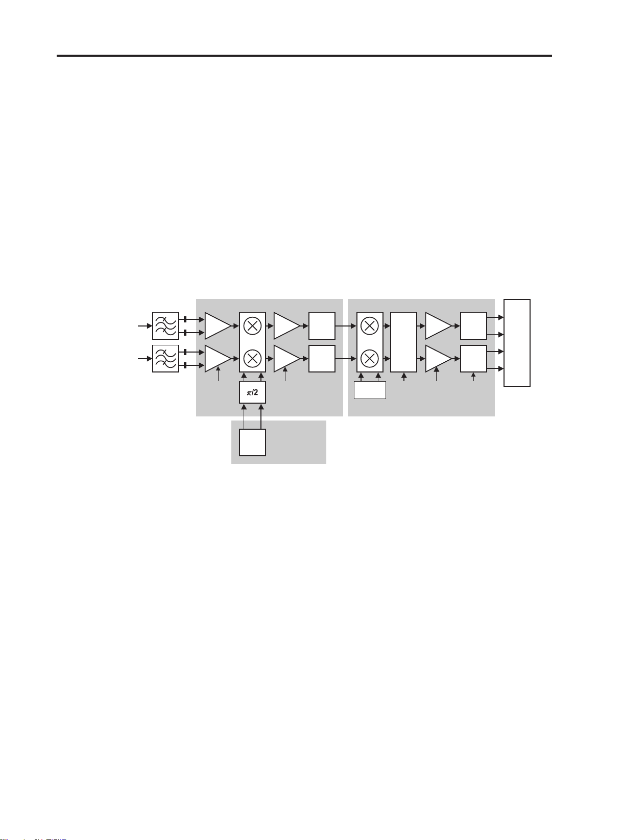
3.2 Receiver Part
A. RF front end
RF front end consists of Antenna Switch(FL401), two SAW Filters(FL402, FL403) dual band LNAs
integrated in transceiver(U401).
The Received RF signals(GSM 925MHz ~ 960MHz, DCS 1805MHz ~ 1880MHz) are fed into the
antenna or Mobile switch. An antenna matching circuit is between the antenna and the mobile
switch.
The Antenna Switch(FL401) is used to control the Rx and Tx paths. And, the input signals VC1 and
VC2 of a FL401 are directly connected to baseband controller to switch either Tx or Rx path on.
Ant S/W module(FL401) is an antenna switch module for dual band phone.
The logic and current is given below table 3-1.
Table 3-1. The logic and current
The receiver part uses a low-IF receiver architecture that allows for the on-chip integration of the
channel selection filters, eliminating the external RF image reject filters and the IF SAW filter
required in conventional super-heterodyne architecture. The Si4200-BM[U401] integrates three
differential input LNAs that are matched to the 200 Ohm balanced-output SAW filters through
external LC matching networks.
B. IF
A quadrature image-rejection mixer downconverts the RF signal to a 100kHz intermediate
frequency(IF) with the RFLO from the Si4133T-BM[U403]. The RFLO frequency is between 1737.8
and 1989.8 MHz, and is divided by two in the Si4200 for GSM850 and E-GSM 900 modes. The
mixer output is amplified with an analog programmable gain amplifier(PGA), which is controlled with
the AGAIN[2:0] bits in register 05h.
The quadrature IF signal is digitized with high resolution A/D converters(ADCs).
The Si4201-BM[U402] downconverts the ADC output to baseband with a digital 100kHz quadrature
LO signal. Digital decimation and IIR filters perform channel selection to remove blocking and
VC1 VC2 Current
GSM TX 0V 2.5 ~ 3.0V 10.0 mA max
DCS TX 2.5 ~ 3.0V 0V 10.0 mA max
GSM/DCS RX 0V 0V < 0.1 mA
3. TECHNICAL BRIEF
- 14 -
reference interference signals.
The response of the IIR filter is programmable to a high selectivity setting(CSEL=0) or a low
selectivity setting(CSEL=1). After channel selection, the digital output is scaled with digital PGA,
which is controlled with the DGAIN[5:0] bits in register 05h.
C. Demodulator and base band processing
The amplified digital output signal go through with DACs that drive a differential analog signal onto
the RXIP,RXIN,RXQP and RXQN pins to interface to standard analog ADC input baseband ICs.
No special processing is required in the baseband for offset compensation or extended dynamic
range.
Compared to a direct-conversion architecture, the low-IF architecture has a much greater degree of
immunity to dc offsets that can arise from RF local oscillator(RFLO) self-mixing, 2nd order distortion
of blockers, and device 1/f noise.
Figure 3-1. RF Receiver path Block diagram
3.3 Synthesizer Part
The synthesizer IC, the Si4133T-BM[U403] is a monolithic CMOS integrated circuit that performs IF
and RF synthesis. Two complete PLLs are integrated including VCOs, varactors, resonators, loop
filters, reference and VCO dividers, and phase detectors. Differential outputs for the IF and RF PLLs
are providedfor direct connection to the Si4200-BM[U401] transceiver IC. The RF PLL uses two
multiplexed VCOs.
The RF1 VCO is used for Receive mode, and the RF2 VCO is used for Transmit mode.
The IF PLL is used only during Transmit mode and uses a single VCO.
The center frequency of each of the three VCOs on the Si4133T is set by connection of an external
inductance(Lext). The IF and RF output frequencies are set by programming the N-Divider
registers,N[RF1],N[RF2], and N[IF]. Programming the N-Divider register for either RF1 or RF2
automatically selects the proper VCO. The output frequency of each PLL is as follows:
fout = N * fø
A programmable divider at the XIN pin allows either a 13 or 26MHz from the external applied crystal
oscillator.
The RF PLL phase detector update rate( fø) can be programmed with the RFUP bit in register 31h
to either fø= 100kHz or fø= 200kHz. The IF PLL always uses fø= 200kHz.
Receive mode should use fø= 100kHz in DCS1800 and PCS1900 bands, and fø= 200kHz in the
GSM850 and E-GSM 900 bands.
Transmit modes should always use fø= 200kHz. The IF and RF output frequencies are set by
GSM
DCS
RXBAND[1:0]
LNAC[1:0]
LNAG[1:0]
AGAIN[2:0]
CSEL DGAIN[5:0]
N
RF1
[15:0]
RFUP
DACCM[1:0]
DACFS[1:0]
ZERODEL[2:0]
U401(Si4200-BM)
Si4133T
U402(Si4201-BM)
I
Q
LNA
PGA ADC
ADC
PGA
PGA DAC
DAC
PGA
CHANNEL
FILTER
BASEBAND
RF
PLL
100 kHz
LNA
LNA

3. TECHNICAL BRIEF
- 15 -
programming the N-Divider registers and also programmed via 3-wire interface with external system
controller.
Figure 3-2. Si4133T Frequency Synthesizer Block Diagram
3.4 Transmitter Part
The Transmitter part contains Si4200-BM[U401] active parts, PAM[U404] and Antenna
Switch[FL401].
The transmit section of Si4200-BM [U401] consists of an I/Q baseband upconverter, an offset
phase-locked loop (OPLL) and two 50 ohm output buffers that can drive external power amplifiers
(PA).
The RF GMSK outputs from the transmit VCO are fed directly to the RF power amplifiers.
The peak output power and the profile of the transmitted burst are controlled by means of
incorporated power control circuits inside of PA and DAC output from the Baseband Controller. The
PA outputs pass to the antenna connector via Antenna Switch.
Figure 3-3. RF Transmit path Block Diagram
XIN
PDNB
SDI
SDO
SCLK
SENB
1, 2
Power
Control
Serial
I/O
RF1
RF2
N
N
65,
130
¿
DET
¿
DET
Self
Tune
Self
Tune
RFLC, RFLD
RFLA, RFLB
IFLOP
IFLON
RFLOP
RFLON
RF PLL
IF PLL
IFLA
IFLB
V403(Si4133 T -BM)
DIV2 RFUP
PDIB
PDRB
SDOSEL[4:0]
N
RF1
[15:0]
N
RF2
[15:0]
N
IP
[15:0]
GSM
DCS
I
Q
2
1, 2
RF
PLL
REG
REG
PA
PA
IF
PLL
BASEBAND
¿
DET
V403(Si4133 T -BM)
V401(Si4200-BM)
N
RF1
[15:0]
PDRB
NIP[15:0]
PDIB
FIF[3:0]
PDG[3:0]
TXBAND[1:0]
BBG[1:0]
SWAP

A. IF Modulator
The baseband converter(BBC) within the GSM chipset generates I and Q baseband signals for the
Transmit vector modulator. The modulator provides more than 40dBc of carrier and unwanted sideband Rejection and produces a GMSK modulated signal. The baseband software is able to cancel
out differential DC offsets in the I/Q baseband signals caused by imperfections in the D/A
converters.
The TX-Modulator implements a quadrature modulator. A quadrature mixer upconverts the
differential I/Q signals with the IFLO to generate a SSB IF signal which is filtered and used as the
reference input to the OPLL. The Si4133T [U403] generates the IFLO frequency. The IFLO is
divided by two to generate The quadrature LO signals for the quadrature modulator.
B. OPLL
The OPLL consists of a feedback mixer, a phase detector, a loop filter, and a fully integrated
TXVCO.
The TXVCO is centered between the DCS 1800 and PCS 1900 bands, and its output is divided by
two for the GSM 850 and E-GSM 900 bands. The Si4133T generates the RFLO frequency between
1272 and 1483 MHz. To allow a single VCO to be used for the RFLO, high-side injection is used for
the GSM 850 and E-GSM 900 bands, and low-side injection is used for the DCS 1800 and PCS
1900 bands.
Low-pass filters before the OPLL phase detector reduce the harmonic content of the quadrature
modulator and feedback mixer outputs. The cutoff frequency of the filters is programmable with
the FIF[3:0] bits in register 04h.
The OPLL requires no external duplexer to attenuate transmitter noise and spurious signals in the
receive band. Additionally, the output of the transmit VCO (TXVCO) is a constant-envelope signal
which reduces the problem of spectral spreading caused by non-linearity in the PA.
C. Power Amplifier
The RF3133 [U404] is a triple-band GSM/DCS/PCS power amplifier module that incorporates an
indirect closed loop method of power control. The indirect closed loop is fully self contained and
does not require loop optimization. It can be driven directly from the DAC output in the baseband
circuit.
On-board power control provides over 37 dB of control range with an analog voltage input(Vramp).
It efficiency is 55% at GSM and 52% at DCS.
Figure 3-4. Power Amplifier Block Diagram
3. TECHNICAL BRIEF
- 16 -
DCS/PCS IN
BAND SELECT
TX ENABLE
VBATT
VREG
VRAMP
GSM IN
GSM OUT
VCC OUT
DCS/PCS
VCC2C2
1
2
3
4
5
6
7
9
10
11
12
8

3. TECHNICAL BRIEF
- 17 -
3.5 13 MHz Clock
The 13 MHz clock(X401) consists of a TCXO(Temperature Compensated Crystal Oscillator) which
oscillates at a frequency of 13 MHz. It is used within the Si4133T/Si4201 RF Main Chip,BB Analog
chip-set(U102 AD6521), Digital(U101 AD6525), and MIDI(U201) Chipset.
Figure 3-5. VCTCXO Circuit
3.6 Power Supplies and Control Signals
There are two regulators used in the phone to provide RF power. One is contained inside of
ADP3522(U302), Power management IC to provide the power for the VCTCXO(X401).
The other is used to provide the power for remaining RF circuits.
Table 3-2. Power supplies and control signals.
Figure 3-6. Regulator
Regulator Voltage Powers Enable Signal
12.75V +/- 0.5V VTCXO 10.0 mA max
2.85V +/- 0.5V RF circuitry RF_EN
Regulator 1
(U302, 2V75_VTCXO)
Regulator 2
(U405, RF2.85V)

3.7 Digital Main Processor
AD6525
Figure 3-7. Example of System interconnection of AD6525 External Interface
3. TECHNICAL BRIEF
- 18 -

3. TECHNICAL BRIEF
- 19 -
Interconnection with external devices
RTC block interface
Countered by external X-TAL
The X-TAL oscillates 32.768KHz
LCD module interface
Main controlled by _MAIN_LCD_CS, _SUBLCD_CS, LCD_RES,
LCD_RS(ADD1),_WR,DATA[00...15] signals.
Table 3-3.
RF interface
The AD6522 control RF parts through TXEN, RXON1, RXON2, AGCEN, PLL_DATA, PLL_CLK,
PLL_LE etc.
Table 3-4.
Description
_MAIN_LCD_CS MAIN LCD driver chip enable. MAIN LCD driver IC has own CS pin
LCD_RES This pin resets LCD module.
LCD_RS (ADD1)
This pin determines whether the data to LCD module are display data or
control data. ADD1 can select 16 bit parallel bus. ADD1 is also used to
address flash memory.
__WR Write control. The phone do not read data from LCD chip.
DATA [00...15] Parallel data lines. Color LCD driver chip uses the 16-bit data interface.
2V8_VMEM 3V voltage is supplied to white colored LED driver for backlighting.
LCD_BACKLIGHT Control signal of white LED driver IC.
_SUBLCD_CS SUB LCD driver chip enable, Sub LCD driver IC has own CS pin.
DATA[08...15] Parallel data lines, Sub LCD driver chip uses the 8-bit data in reface.
GPO
Signal
Description Reset
Name
0 RXON RX Enable/Disable L
1 TXON TX Enable/Disable L
4 RF_EN RF LDO Enable/Disable L
8 VREG
Regulating Voltage input
L
for Power Control function
(2.8V nominal)
9 ANT_SW1
Antenna Switch Band Select
L
(DCS Band)
10 ANT_SW1
Antenna Switch Band Select
L
(GSM Band)
16 PA_EN PAM Enable/Disable L
17 PA_BAND PAM Band Selectl
18 PDNB Powerdown Input L
19 S_EN Serial Enable Input L
20 S_DATA Serial Data Input L
21 S_CLK Serial Clock Input L

3. TECHNICAL BRIEF
- 20 -
SIM interface
The AD6525 check status periodically in call mode if SIM card is inserted or not, but the AD6525
don't check in deep sleep mode.
Interface by SIMDATAOP, SIMCLK, SIM_RST(GPIO_23)
Table 3-5.
SIM CONNECTOR
Figure 3-8. SIM Interface of AD6525
Key interface
Include 5 column and 5 row. The AD6522 detect key press by interrupt.
ADP3522 interrupt
There are two interrupts EOC and CHARGEDET
EOC: End of Charge. AD6525 makes charging operation stop when high signal is inputted.
CHARGEDET: This pin is activated when the charger is inserted.
Description
SIMDATAOP This pin receives and sends data to SIM card. This model support 1.8volt
or 3.0 volt interface SIM card.
SIMCLK Clock 3.25MHz frequency.
SIM_RST(GPIO_23) Reset SIM block.
Description
SIMDATAOP
This pin receives and sends data to SIM card. This model support
1.8volt or 3.0 volt interface SIM card.
SIMCLK Clock 3.25MHz frequency.
SIM_RST(GPIO_23) Reset SIM block.
3. TECHNICAL BRIEF
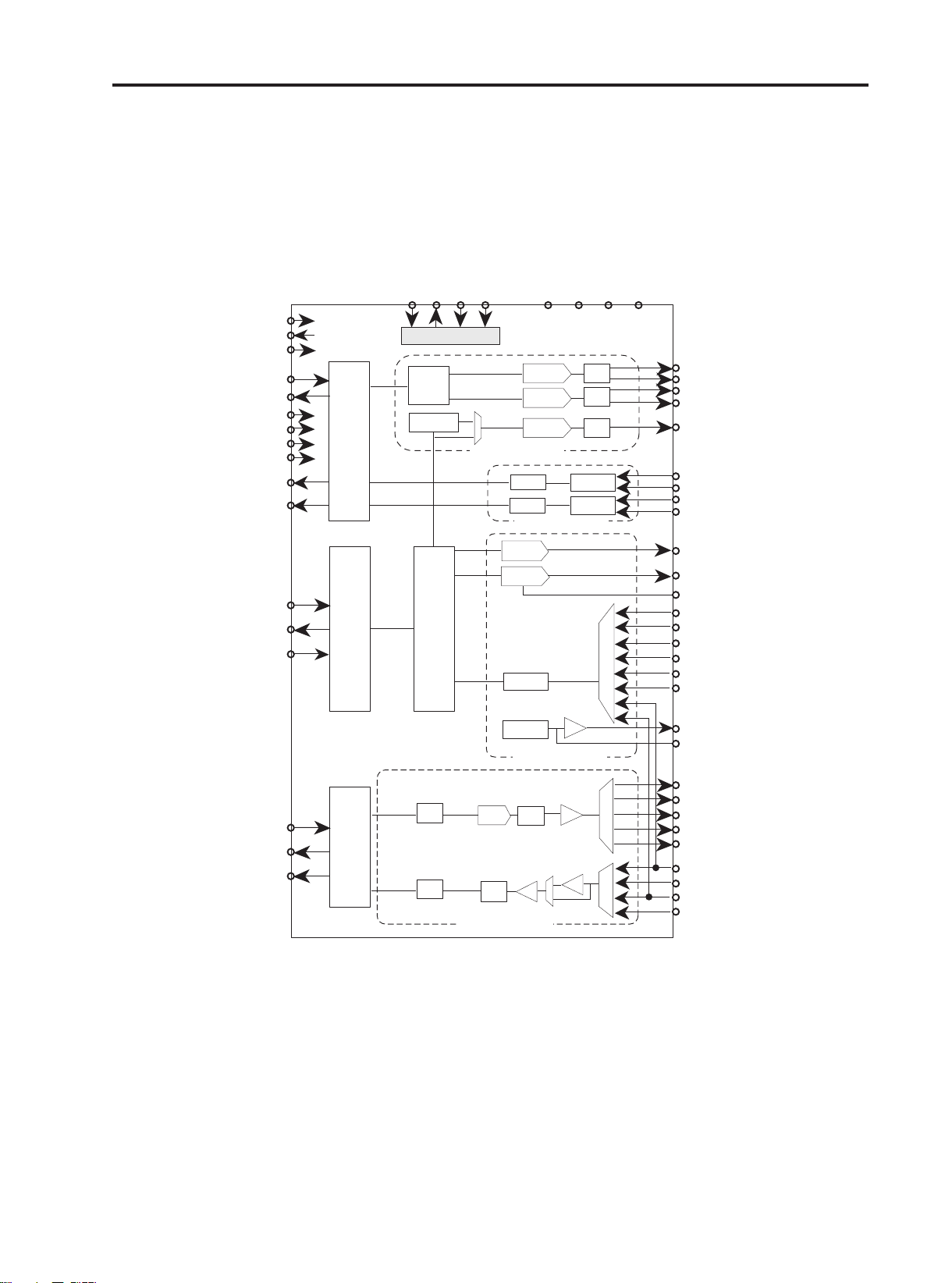
- 21 -
3.8 Analog Main Processor
AD6521
Figure 3-9. AD6521 function block diagram
AUXILIARY
SERIAL
PORT
CONTROL
REGISTERS
CMEK MOD
32X10-BIT
RAMP RAM
I TRANSMIT
DAC
Q TRA NSMIT
DAC
10-BIT
RAMP DAC
13-BIT
AFC DAC
10-BIT
IDAC
FILTER
FILTER
FILTER
FILTER
I RECEIVE
DCC
Q RECEIVE
DCC
10-BIT
AUXADC
VOLTAGE
REFERENCE
AUXILIARY SECTION
VOICEBAND SECTION
BASEBAND RECEIVE SECTION
BASEBAND TRANSMIT SECTION
FILTER
VOICEBAND
SERIAL
PORT
FILTER
DAC
PGA
PGA
MIC
FILTER
FILTER
ADC
JTAG INTERFACE
MCLK
TDI TDO TMS TCK AVDD DVDD AGND DGND
ITXP
ITXN
QTXP
QTXN
RAMPDAC
IRXP
IRXN
QRXP
QRXN
AUXADC2
AUXADC3
AUXACD4
AUXADC5
AUXADC6
REFOUT
REFCAP
VOUTNORP
VOUTNORN
VOUTAUXP
VOUTAUXN
BUZZER
VINNORP
VINNORN
VINAUXP
VINAUXN
IDACOUT
IDACREF
AFCDAC
AUXADC1
MCLKEN
RESET
BSDI
BSIFS
TXON
ATSM
RXON
ARSM
BSDO
BSOFS
ASDI
ASDO
ASFS
VSDI
VSDO
VSFS
BASEBAND
SERIAL
PORT
AD6521
Dual-Mode Voiceband B aseband Codec

BB Transmit section
This section generates in-phase and quadrature BB modulated GMSK signals (BT = 0.3) in
accordance with GSM 05.05 Phase 2 specifications.
The transmit channel consists of a digital GMSK modulator, a matched pair of 10-bit DACs and a
matched pair of reconstruction filter.
BB Receive section
This section consists of two identical ADC channels that process baseband in-phase(I) and
quadrature(Q) input signals.
Each channel consists of a coarse switched capacitor input filter, followed by a high-order sigma-
delta modulator and a lowpass digital filter.
Auxiliary section
This section contains two auxiliary DACs(AFC DAC, IDAC) for system control.
This section also contains AUX ADC and Voltage Reference
AUX ADC : 6 channel 10 bits
AFC DAC : 13 bits
IDAC : 10 bits
Voiceband section
Receive audio signal from MIC. The phones use differential configuration.
Send audio signal to Receiver. The phones use differential configuration.
It interconnects external devices such as main microphone, main receiver, ear-phone and Hands
free kit through the VINNORP, VINNORN, VOUTNORP, VOUTNORN, VINAUXP, VINAUXN,
VOUTAUXP, VOUTAUXN
VINNORP, VINNORN: Main MIC positive/negative terminal.
VOUTNORP, VOUTNORN: Main Receiver positive/negative terminal.
VINAUXP, VINAUXN: Hands free kit microphone positive/negative terminal.
VOUTAUXP, VOUTAUXON: Hands free kit speaker positive/negative terminal.
3. TECHNICAL BRIEF
- 22 -

Figure 3-10. Voice band circuit diagram
3. TECHNICAL BRIEF
- 23 -

3. TECHNICAL BRIEF
- 24 -
Figure 3-11. Voice band circuit diagram

3. TECHNICAL BRIEF
- 25 -
3.9 Power Management IC
Figure 3-12. ADP3522 inner block diagram
Table 3-6.
Description
VSIM 2.85V(is provided to SIM card)
VCORE 1.8V(is provided to the AD6525 & AD6521’s digital core)
VRTC 2.0V(is provided to the RTC and Backup Battery)
VAN 2.55V(is provided to the AD6521 I/O and used as microphone bias)
VTCXO 2.75V(is provided to VCTCXO)
VMEM 2.8V(is provided to Flash)

3. TECHNICAL BRIEF
- 26 -
Power up sequence logic
The ADP3522 controls power on sequence.
Power on sequence
If a battery is inserted, the battery powers the 6 LDOs.
Then if PWRONKEY is detected, the LDOs output turn on.
REFOUT is also enabled, Reset is generated and send to the AD6525.
LDO block
There are 6 LDOs in the ADP3522.
Battery charging block
It can be used to charge Lithium Ion and/or Nickel Metal Hydride batteries. The phones use Li-Ion
battery only. Charger initialization, trickle charging, and Li-Ion charging control are implemented in
hardware.
Charging Process
1. Check charger is inserted or not.
2. If ADP3522 detects that Charger is inserted, the CC-CV charging starts.
3. Exception: When battery voltage is lower than 3.2V, the precharge (low current charge mode)
starts firstly.
4. And the battery voltage reach to 3.2V the CC-CV charging starts.
Pins used for charging
CHGDET : Interrupt to AD6525 when charger is plugged.
CHGEN : Control signal from AD6525 to charge Li+ battery.
EOC : Interrupt to AD6525 when battery is fully charged.
GATEIN : Control signal from AD6525 to charge NiMH battery. But, not used.
MVBAT : Battery voltage divider. Divide ratio is 1:2.3 and it is sensed in AD6521 AUX_ADC4.
TA (Travel Adaptor)
Input voltage : AC 85V ~ 264V, 47~63Hz
Output voltage : DC 5.2V(±0.2 V)
Output current : Max 750mA(±50mA )
Battery
Li-ion battery : Max 4.2V, Nom 4.0V
Standard battery : Capacity - 740mAh, Li-ion
3. TECHNICAL BRIEF
- 27 -
3.10 Memories
128Mbit flash memory + 32Mbit PSRAM
16 bit parallel data bus
ADD01 ~ ADD22.
2 Chip enables for Flash memory select.
RF Calibration data, Audio parameters and battery calibration data etc are stored in
Flash memory area.
3.11 Display and Interface
Table 3-7.
G5400 Main LCD supports one 65000 color resolution LCD module.
There are the control signals :_MAIN_LCD_CS (which is derived from AD6525, this acts
as the chip select enable for the LCD), _WR, LCD_RS and LCD_RES. AD6525 uses DATA[00:15]
pins to send data for displaying graphical text onto the LCD.
G5400 Sub LCD supports one 65000 mono resolution LCD module.
There are the control signals :_SUBLCD_CS (which is derived from AD6525, this acts as the chip
select enable for the LCD), _WR, LCD_RS and LCD_RES. AD6525 uses DATA[08:15] pins to send
data for displaying graphical text onto the LCD.
LCD
Main LCD Display Format 128×RGB×160dots
Main LCD Backlight White LED Backlight
Sub LCD Display Format 96×16dots
Sub LCD Backlight 7Color LED Backlight
3. TECHNICAL BRIEF
- 28 -
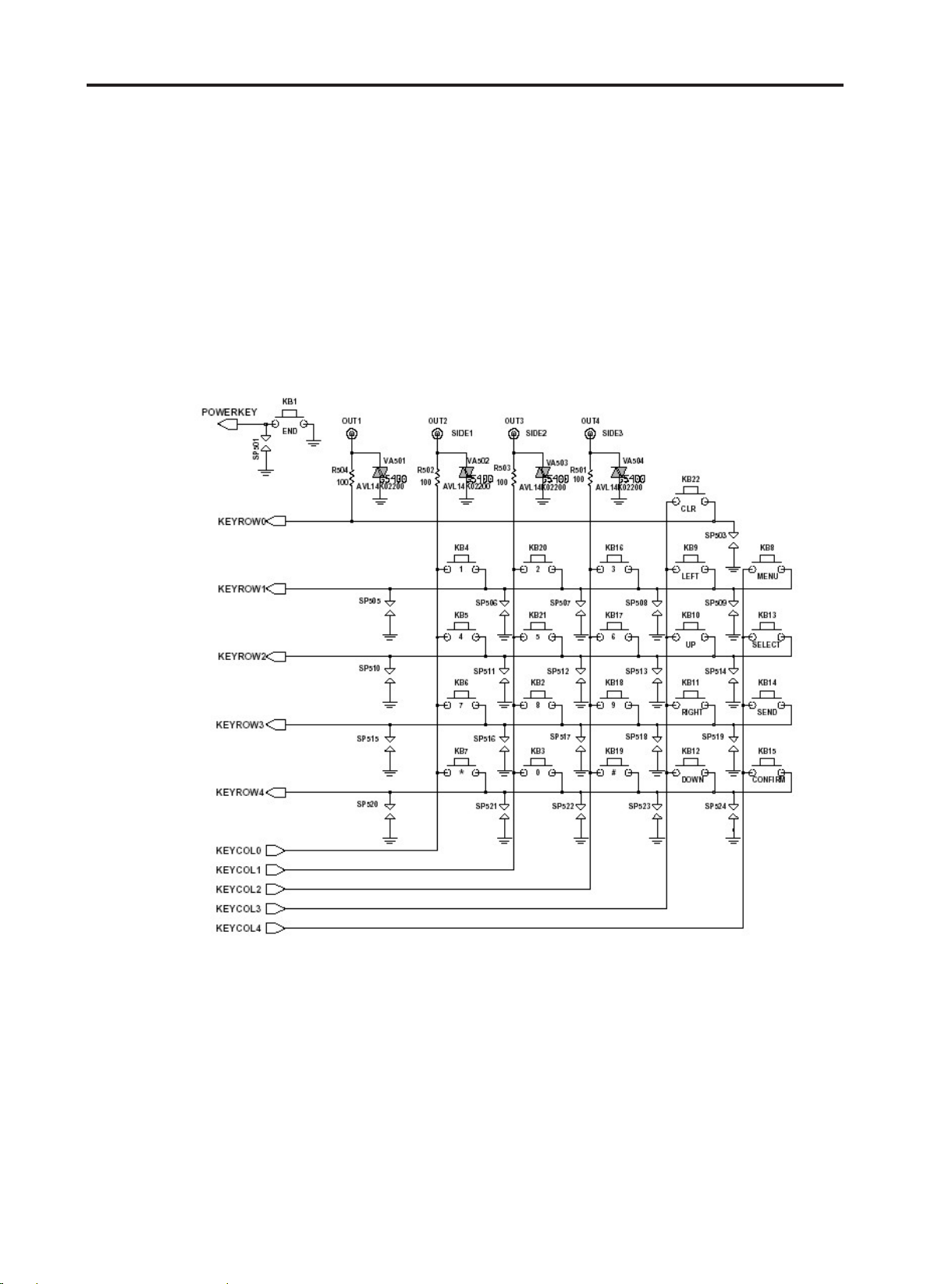
3.12 Keypad Switches and Scanning
The key switches are metal domes, which make contact between two concentric pads on the
keypad layer of the PCB when pressed. There are 25 switches (KB1-KB22), connected in a matrix
of 5 rows by 5 columns, as shown in Figure, except for the power switch (KD110), which is
connected independently. Functions, the row and column lines of the keypad are connected to ports
of AD6525. The columns are outputs, while the rows are inputs and have pull-up resistors built in.
When a key is pressed, the corresponding row and column are connected together, causing the row
input to go low and generate an interrupt. The columns/rows are then scanned by AD65225 to
identify the pressed key.
Figure 3-13. Keypad Switches and Scanning
3. TECHNICAL BRIEF
- 29 -
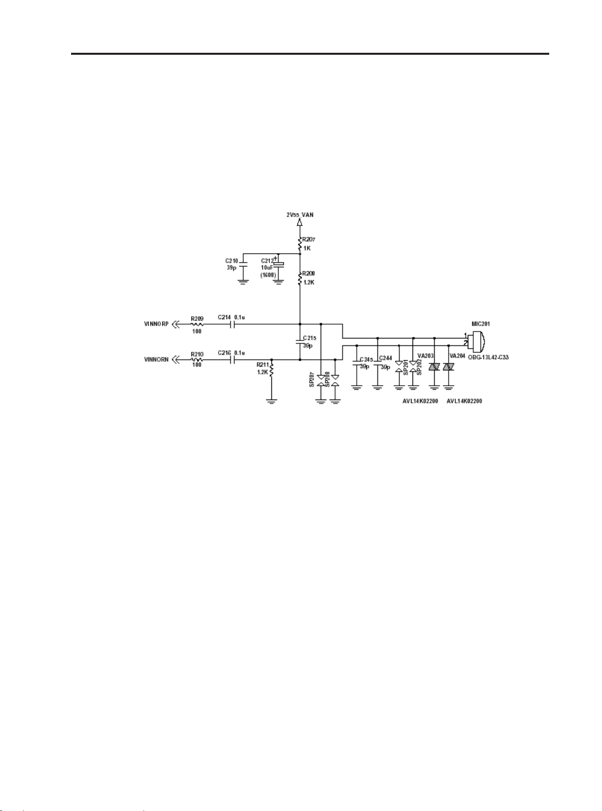
3.13 Microphone
The microphone is placed to the front cover and contacted to main PCB. The audio signal is passed
to VINNORP (#J10) and VINNORN (#K10) pins of AD6525. The voltage supply 2V55_VAN is output
from ADP3522, and is a bias voltage for the VINNORP. The VINNOR or VINAUX signal is then A/D
converted by the Voiceband ADC part of AD6521. The digitized speech is then passed to the DSP
section of AD6525 for processing (coding, interleaving etc.).
Figure 3-14. Microphone

3. TECHNICAL BRIEF
- 30 -
3.14 Earpiece
The earpiece is driven directly from AD6521 VOUTNORP (#K8) and VOUTNORN (#K7) pins and
the gain is controlled by the PGA in an AD6521.
The earpiece is placed in the folder cover and contacted to LCD PCB.
Figure 3-15. Earpiece
3.15 Hands-free Interface
The audio out (VOUTAUXP & VOUTAUXN) to the hands-free kit consists of a pair of differential
signal from AD6521 auxiliary outputs (#K9, #K6), which are tracked down the board to carkit
connector (CN602) at the base of the handset. The DC level of the signal is supplied to the
VOUTAUX pin.
3.16 Headset Jack Interface
This phone chooses a 3-pole type ear-mic jack which has three electrodes such as Receiver +,
Mic+, and GND. This type usually supports only single-ended configuration in the audio path. But
most of phones use the common interface.
3. TECHNICAL BRIEF
- 31 -
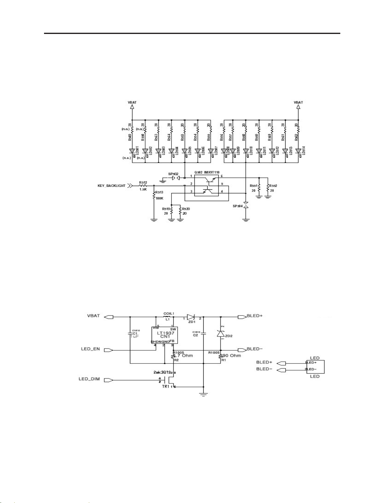
3.17 Key Back-light Illumination
In key back-light illumination, there are 12 Blue LEDs in Main Board, which are driven by
KEY_BACKLIGHT line from AD6525.
Figure 3-16. Key Back-light Illumination
3.18 LCD Back-light Illumination
In LCD Back-light illumination, there is an driver in LCD Board, which is driven by BACKLIGHT
line from AD6525.
Figure 3-17. Main LCD Back light Illumination
 Loading...