LG G1500 Service Manual

REVISED HISTORY
DATE ISSUE CONTENTS OF CHANGES S/W VERSION
Initial Release
The information in this manual is subject to change without notice and should not be construed as
a commitment by LGE Inc. Furthermore, LGE Inc. reserves the right, without notice, to make
changes to equipment design as advances in engineering and manufacturing methods warrant.
This manual provides the information necessary to install, program, operate and maintain the
G1500.
-1-

Table Of Contents
1. INTRODUCTION................................…5
1.1 Purpose ............................................….
1.2 Regulatory Information ..........................
1.3 Abbreviations .........................................
5
5
7
2. PERFORMANCE ..............................….9
2.1 H/W Features .....................................…..
2.2 Technical Specification ..........................
10
3. TECHNICAL BRIEF ............................16
3.1 General Description ......……..…………..
3.2 Receiver .............................................….
3.3 Transmitter Part …..………………………
3.4 13MHz Clock …………………….........….
3.5 Power Supplies for RF Circuits ………….
3.6 Testing Set-up and Checking Signals ..….
3.7 Digital Main Processor ….....................….
3.8 Analog Main Processor ……..................…
3.9 Power Management …….....................….
3.10 Memories ................................................
3.11 Display and Interface ..............................
3.12 Keypad Switches and Scanning ........... .
3.13 Microphone ..................………………..…
3.14 Earpiece …………………………………...
3.15 Headset Jack Interface ……..............….
3.16 Key Back-light Illumination ………..……
3.17 LCD Back-light Illumination ……………..
3.18 Speaker & MIDI IC ……………………….
16
16
19
22
22
23
36
41
44
46
46
46
47
49
49
49
50
51
4. TROUBLESHOOTING .................… 52
4.1 RF Components .............................….
4.2 Rx Trouble ..........................................
4.3 Tx Trouble ..........................................
4.4 Power On Trouble ..........................….
4.5 Charging Trouble ...........................….
4.6 LCD Trouble .......................................
9
4.7 Receiver Trouble ................................
4.8 Speaker Trouble .................................
4.9 Mic. Trouble ...................................….
4.10 Vibrator Trouble ...............................
4.11 Backlight LED Trouble ......................
4.12 SIM Detect Trouble ..........................
4.13 Earphone Trouble ............................
52
53
61
74
76
78
80
82
84
87
89
91
93
5. DISASSEMBLY INSTRUCTION ...... 97
5.1 Disassembly .........................................
97
6. DOWNLOAD AND
CALIBRATION ……………............. 100
6.1 Download ……….............................…..
6.2 Calibration …………........................…..
100
102
7. BLOCK DIAGRAM ........................... 105
-3 -

8. CIRCUIT DIAGRAM ......................... 107
8.1 Main Chipset ………………….............…..
8.2 Memory & MMI …………….........……….
8.3 MIDI ……………………………….......….
8.4 RF Circuit ……..................................…..
107
108
109
110
9. PCB LAYOUT .................................. 111
10. STAND ALONE TEST ................... 113
10.1 What’s the Standalone Test? .....……
10.2 Standalone Test Equipment Setup…
10.3 H/W Test …….............................……
10.4 Tx Stand alone Test Setting …………..
10.5 Rx Stand alone Test Setting …………..
10.6 What’s the Rx Calibration …………….
10.7 What’s the Tx Calibration ……………..
10.8 How to Rx Calibration …………………
10.9 How to Tx Calibration ………………….
10.10 Target powers in dBm for each
power level ……………………………..
113
114
115
116
118
120
120
121
121
121
11. EXPLODED VIEW &
REPLACEMENT PART LIST ...…. 127
11.1 Exploded View ...........................……
11.2 Accessory ...............................……..
11.3 Replacement Parts
< Mechanic component > ……………..
Replacement Parts
< Main component > ………………….
127
129
130
132
-4 -

1. INTRODUCTION
1. INTRODUCTION
1.1 Purpose
This manual provides the information necessary to repair, calibration, description and download the
features of LG-G1500.
1.2 Regulatory Information
A. Security
Toll fraud, the unauthorized use of telecommunications system by an unauthorized part (for example,
persons other than your company’s employees, agents, subcontractors, or person working on your
company’s behalf) can result in substantial additional charges for your telecommunications services.
System users are responsible for the security of own system. There may be risks of toll fraud associated
with your telecommunications system. System users are responsible for programming and configuring the
equipment to prevent unauthorized use. The manufacturer does not warrant that this product is immune
from the above case but will prevent unauthorized use of common-carrier telecommunication service of
facilities accessed through or connected to it. The manufacturer will not be responsible for any charges
that are resulted from such unauthorized use.
B. Incidence of Harm
If a telephone company determines that the equipment provided to customer is faulty and possibly
causing harm or interruption in service to the telephone network, it should disconnect telephone service
until repair can be done. A telephone company may temporarily disconnect service as long as repair is
not done.
C. Changes in Service
A local telephone company may make changes in its communications facilities or procedure. If these
changes could reasonably be expected to affect the use of this phone or compatibility with the network,
the telephone company is required to give advanced written notice to the user, allowing the user to take
appropriate steps to maintain telephone service.
D. Maintenance Limitations
Maintenance limitations on this model must be performed only by the manufacturer or its authorized agent.
Therefore, note that unauthorized alternations or repair may affect the regulatory status of the system and
may void any remaining warranty.
E. Notice of Radiated Emissions
The LG-G1500 complies with rules regarding radiation and radio frequency emission as defined by local
regulatory agencies. In accordance with these agencies, you may be required to provide information such as
the following to the end user.
-5 -

1. INTRODUCTION
F. Pictures
The pictures in this manual are for illustrative purposes only; your actual hardware may look slightly different.
G. Interference and Attenuation
The LG-G1500 may interfere with sensitive laboratory equipment, medical equipment, etc. Interference from
unsuppressed engines or electric motors may cause problems.
H. Electrostatic Sensitive Devices
ATTENTION
Boards, which contain Electrostatic Sensitive Device (ESD), are indicated by the sign.
Following information is ESD handling:
• Service personnel should ground themselves by using a wrist strap when exchange system
boards.
• When repairs are made to a system board, they should spread the floor with anti-static mat
which is also grounded.
• Use a suitable, grounded soldering iron.
• Keep sensitive parts in these protective packages until these are used.
• When returning system boards or parts like EEPROM to the factory, use the protective
package as described.
-6 -

1.3 Abbreviations
For the purposes of this manual, following abbreviations apply:
Automatic Power ControlAPC
BasebandBB
Bit Error RateBER
Constant Current – Constant VoltageCC-CV
Digital to Analog ConverterDAC
Digital Communication SystemDCS
1. INTRODUCTION
dB relative to 1 milli wattdBm
Digital Signal ProcessingDSP
Electrostatic DischargeESD
Flexible Printed Circuit BoardFPCB
Gaussian Minimum Shift KeyingGMSK
General Purpose Interface BusGPIB
Global System for Mobile CommunicationsGSM
International Portable User IdentityIPUI
Intermediate FrequencyIF
Liquid Crystal DisplayLCD
Low Drop OutputLDO
Light Emitting DiodeLED
Offset Phase Locked LoopOPLL
-7 -

1. INTRODUCTION
Power Amplifier ModulePAM
Printed Circuit BoardPCB
Programmable Gain AmplifierPGA
Phase Locked LoopPLL
Public Switched Telephone NetworkPSTN
Radio FrequencyRF
Receiving Loudness RatingRLR
Root Mean SquareRMS
Real Time ClockRTC
Surface Acoustic WaveSAW
Subscriber Identity ModuleSIM
Sending Loudness RatingSLR
Static Random Access MemorySRAM
Pseudo SRAMPSRAM
Side Tone Masking RatingSTMR
Travel AdapterTA
Time Division DuplexTDD
Time Division Multiple AccessTDMA
Universal Asynchronous Receiver/TransmitterUART
Voltage Controlled OscillatorVCO
Voltage Control Temperature Compensated Crystal OscillatorVCTCXO
Wireless Application ProtocolWAP
-8 -
2. PERFORMANCE
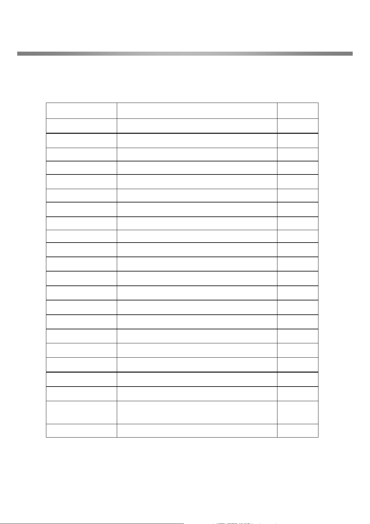
2.1 H/W Features
Item Feature Comment
Support Dual band (EGSM/DCS) Bar Type GPRS
Size 105.2 × 45.6 × 21.3 mm (Max)
Weight 80g (Standard battery)
Battery 3.7V > 850mAh Li-Ion (Standard)
Talk Time (PL : 7) 3hours (Min) at 850mAh (Standard)
Standby Time (PL : 9) 200hours (Min) at 850mAh (Standard)
ANT Type Internal Antenna
2. PERFORMANCE
LCD 128 × 64 Dot, B/W
Back Light LED Back Light
Back Light Color Blue Color
Vibrator Yes (Coin Type)
LED Indicator Use LCD Backlight
Buzzer Yes
C-MIC Yes
Receiver Yes
Earphone Jack Yes (3 Pole Type)
SIM Socket Yes (SIM Block Type)→3V only
Volume key Navigation Key
Voice Dialing Yes
I/O Connect 18 Pin (Batt. 3Pole)
Basic ACC’Y
Option Hand/Neck Strap, Data Kit, CLA, CD
Travel Adapter(3hour-Charging Time)Standard Battery
(LI-Ion 850mAh)Earphone (include Hook Switch)
-9 -

2. PERFORMANCE
2.2 Technical Specification
Item Description Specification
1 Frequency Band
GSM
TX: 890 + n × 0.2 MHz
RX: 935 + n × 0.2 MHz (n=1~124)
EGSM
TX: 890 + (n-1024) × 0.2 MHz
RX: 935 + (n-1024) × 0.2 MHz (n=975~1024)
DCS
TX: 1710 + (n-512) × 0.2 MHz
RX: 1805 + (n-512) × 0.2 MHz (n=512~885)
2 Phase Error
3 Frequency Error < 0.1 ppm
4 Power Level
RMS < 5 degrees
Peak < 20 degrees
GSM, EGSM
Level Power Toler. Level Power Toler.
5 33dBm ±2dB 13 17dBm ± 3dB
6 31dBm ±3dB 14 15dBm ± 3dB
7 29dBm ±3dB 15 13dBm ± 3dB
8 27dBm ±3dB 16 11dBm ± 5dB
9 25dBm ±3dB 17 9dBm ± 5dB
10 23dBm ±3dB 18 7dBm ± 5dB
11 21dBm ±3dB 19 5dBm ± 5dB
12 19dBm ±3dB
DCS
Level Power Toler. Level Power Toler.
0 30dBm ±2dB 8 14dBm ± 3dB
1 28dBm ±3dB 9 12dBm ± 4dB
2 26dBm ±3dB 10 10dBm ± 4dB
3 24dBm ±3dB 11 8dBm ± 4dB
4 22dBm ±3dB 12 6dBm ± 4dB
5 20dBm ±3dB 13 4dBm ± 4dB
6 18dBm ±3dB 14 2dBm ± 5dB
7 16dBm ±3dB 15 0dBm ± 5dB
- 10 -
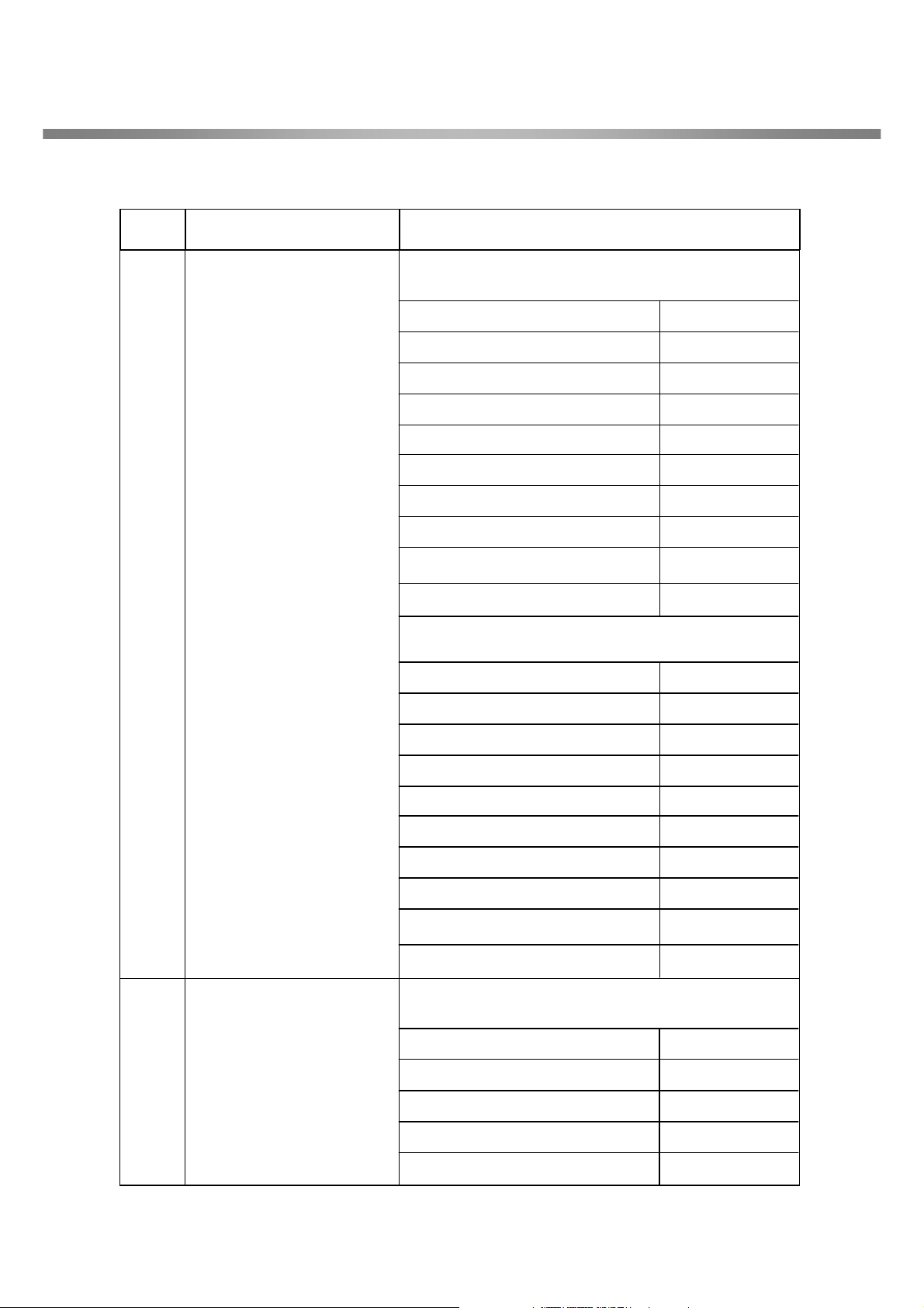
Item Description Specification
GSM, EGSM
Offset from Carrier (kHz). Max. dBc
100 +0.5
200 -30
250 -33
400 -60
600~ <1,200 -60
1,200~ <1,800 -60
1,800~ <3,000 -63
2. PERFORMANCE
3,000~ <6,000 -65
5
Output RF Spectrum
(due to modulation)
DCS
Offset from Carrier (kHz). Max. dBc
GSM, EGSM
6,000 -71
100 +0.5
200 -30
250 -33
400 -60
600~ <1,200 -60
1,200~ <1,800 -60
1,800~ <3,000 -65
3,000~ <6,000 -65
6,000 -73
Offset from Carrier (kHz). Max. dBm
Output RF Spectrum
6
(due to switching
transient)
- 11 -
400 -19
600 -21
1,200 -21
1,800 -24
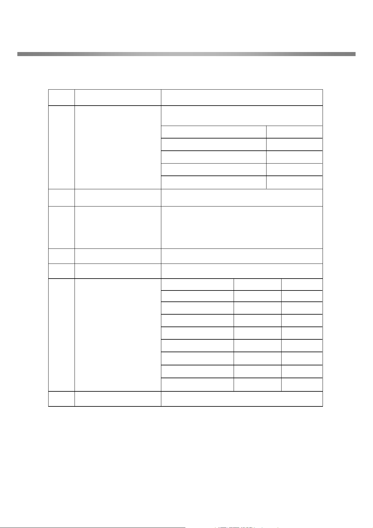
2. PERFORMANCE
Item Description Specification
DCS
Offset from Carrier (kHz). Max. dBm
Output RF Spectrum
6
7 Spurious Emissions Conduction, Emission Status
8 Bit Error Ratio
(due to switching
transient)
GSM, EGSM
BER (Class II) < 2.439% @-102 dBm
DCS
BER (Class II) < 2.439% @-100 dBm
400 -22
600 -24
1,200 -24
1,800 -27
9 RX Level Report Accuracy ±3 dB
10 SLR 8±3 dB
Frequency (Hz) Max.(dB) Min.(dB)
11 Sending Response
12 RLR 2±3 dB
100 -
200 -
300 -12
1,000 -6
2,000 -6
3,000 -6
3,400 -9
4,000 -
-12
0
0
0
4
4
4
0
- 12 -

Item Description Specification
Frequency (Hz) Max.(dB) Min.(dB)
2. PERFORMANCE
13 Receiving Response
* Mean that Adopt a straight line in between 300 Hz
and 1,000 Hz to be Max. level in the range.
14 STMR 13±5 dB
15 Stability Margin > 6 dB
dB to ARL (dB) Level Ratio (dB)
100 -
200 -
300 -7
500 -5
1,000 -5
3,000 -5
3,400 -10
4,000
-35
-30
-12
0
2
*
0
2
2
2
17.5
22.5
-20
16 Distortion
17 Side Tone Distortion Three stage distortion < 10%
18
19 32.768KHz tolerance ≤ 30 ppm
20 Power Consumption
System frequency
(13 MHz) tolerance
≤ 2.5 ppm
Full power
< 243mA (GSM,EGSM), < 209mA (DCS)
Standby
Normal < 4mA (Max. power)
-10
0
7
10
30.7
33.3
33.7
31.7
25.5
- 13 -

2. PERFORMANCE
Item Description Specification
21 Talk Time
22 Standby Time
23 Ringer Volume
24 Charge Voltage
25 Antenna Display
GSM/Level 7 (Battery Capacity 850mA): Up to 180 Min
GSM/Level 12 (Battery Capacity 850mA): Up to 300 Min
Under conditions, Up to 200hours:
1. Brand new and full 850mAh battery
2. Full charge, no receive/send and keep GSM in idle
mode.
3. Broadcast set off.
4. Signal strength display set at 3 level above.
5. Backlight of phone set off.
At least 80dB under below conditions:
1. Ringer set as ringer.
2. Test distance set as 50cm
Fast Charge: < 500mA
Slow Charge: < 60mA
Antenna Bar Number Power
5
4
3
2
-85 dBm ~
-90 dBm ~ -86 dBm
-95 dBm ~ -91 dBm
-100 dBm ~ -96 dBm
1
0
Battery Bar Number Voltage
0
26 Battery Indicator
3.5 ± 0.03V (Call)
27 Low Voltage Warning
3.62 ± 0.03V (Standby)
28 Forced shut down Voltage 3.35 ± 0.03V
1 Li-ion Battery
29 Battery Type
Standard Voltage = 3.7 V
Battery full charge voltage = 4.2 V
Capacity: 850mAh
1
2
3
-105 dBm ~ -101 dBm
~ -105 dBm
~ 3.62 V
3.62 ~ 3.73 V
3.73 ~ 3.82 V
3.82 V ~
- 14 -

Item Description Specification
Switching-mode charger
27 Travel Charger
Input: 100 ~ 240 V, 60 Hz
Output: 5.2 V, 800 mA
2. PERFORMANCE
- 15 -
3. TECHNICAL BRIEF
3. TECHNICAL BRIEF
3.1 General Description
The RF parts consists of a transmitter part,a receiver part,a synthesizer part,a voltage supply part,a
VCTCXO part. And the main RF Chipset CX74017[U441]is a single-chip dual-band transceiver for the
extended global system for mobile communication[E-GSM900MHz]/
Digital communication system[DCS1800MHz] voice and data transfer applications.
This device integrated a direct conversion receiver architecture, which eliminates the need of
Intermediate Frequency, a transmitter based on a modulation loop architecture and fractional-N
synthesizer part with built in TXVCO and Local-VCO.
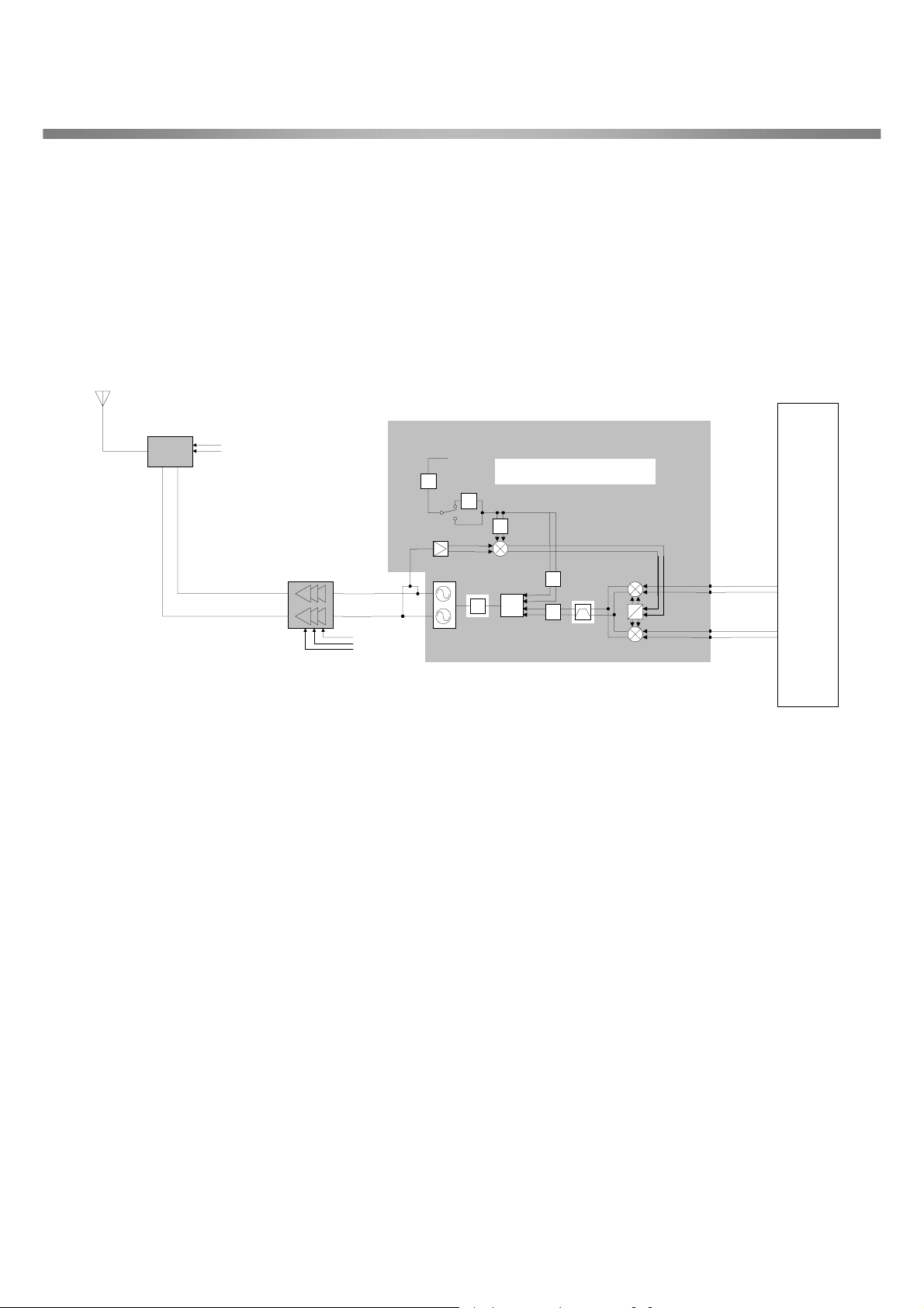
3.2 Receiver
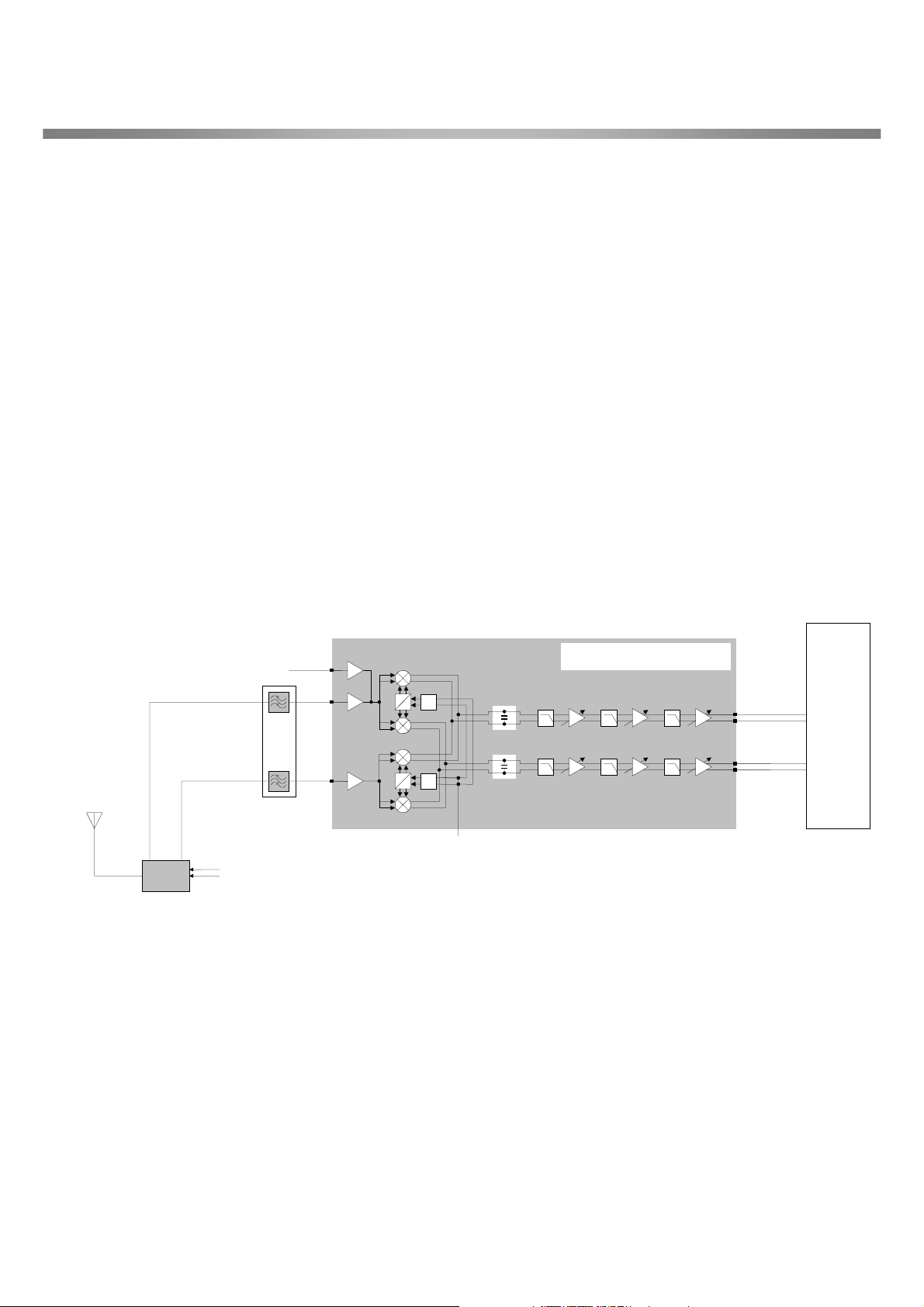
The Receiver part in CX74017 contains all active circuits completely, full receiver chain with the
exception of discrete front-end RF SAW filters. The filtered and amplified signal is down converted in
the RF-mixer to the baseband output. The receiver path is supported by internal channel filtering.
The RF front-end circuit is shown Fig. 3-1.
LMSP54AA-097
DCS : 1805 ~ 1880MHz
GSM : 925 ~ 960MHz
ANT
S/W
GSMSEL
DCSSEL
PCS : 1805 ~ 1880MHz
FAR-G6CS-1G8425-L257
0
4/3
90
0
2/3
90
vco
f
Figure. 3-1 RF Front-end Circuit
CX74017
RXQP
RXQN
RXIP
RXIN
Base
Band
Block
- 16 -

3. TECHNICAL BRIEF
A. RF Front End
RF front end consists of Antenna Switch(FL407), dual band LNAs integrated in transceiver(U441).
The Received RF signals (GSM 925MHz ∼ 960MHz, DCS 1805MHz ∼ 1880MHz) are fed into the
antenna or mobile switch. An antenna matching circuit is between the antenna and the mobile switch.
The Antenna Switch (FL407) is used to control the Rx and TX paths. And, the input signals VC1 and
VC2 of a FL407 are connected to DCSSEL(GPO_9) and GSMSEL(GPO_11) ports of U105 to switch
either TX or RX path on. When the RX path is turned on, the received RF signal then feeds either Rx
_900_RF or RX_1800_RF path controlled by GSM-RX and DCS-RX respectively. This Rx_900_RF
path contains one SAW filter, followed after the Antenna Switch (FL407), to filter any unwanted signal
apart from the DCS RX band. And, the RX_1800_RF path is the same case.
The logic and current for Antenna Switch is given below Table 3-1
Table 3-1 The logic and current
CurrentVC2VC1
10.0 mA max2.7 V0 VGSM TX
10.0 mA max0 V2.7 VDCS TX
<0.1 mA0 V0 VGSM/DCS RX
These two paths are then connected to the LNAGSMN (#11) and LNADCSIN (#13) of CX74017 (U
441), respectively. A low-noise bipolar RF amplifier, contained within the U441, amplifies the RF
signal. The RF signals from the front-end pass to the receiver mixers within the U441 device.
B. Demodulator and baseband processing
In direct conversion receiver there is only one mixer down-converting received RF signal to BB signal
directly. The gain down converting mixer is 40dB at high gain mode and 22dB at low gain mode.
The Rx gain setting is done in the AGC algorithm. The nominal gain of the receiver is set as a
function of the expected signal strength at the antenna input so that a desired level is reached at the
Rx I/Q. 7 blocks in the receiver chain have variable gains, LNA, Mixer, LPF1, VGA1, gmC Filter,
Auxiliary gain control and VGA2. The gain settings can be adjustable via 3-wire bus control lines.
The baseband signals pass via integrated low-pass filters to the baseband A/D converters.
The remainder of the channel filtering is performed by the baseband chipset. The demodulator
contains switches to maintain the sense of the baseband I/Q outputs with respect to the incoming RF
signal on both GSM900 and DCS1800.
- 17 -

3. TECHNICAL BRIEF
C. DC offset compensation
Three correction loops ensure that DC offsets, generated in the CX74017, do not overload the
baseband chain at any point.
After compensation, the correction voltages are held on capacitors for the duration of the
receive slot(s). A rising edge on the RXEN signal, selected via the serial interface, placed the
DC compensation circuitry in the track mode.
- 18 -
3. TECHNICAL BRIEF
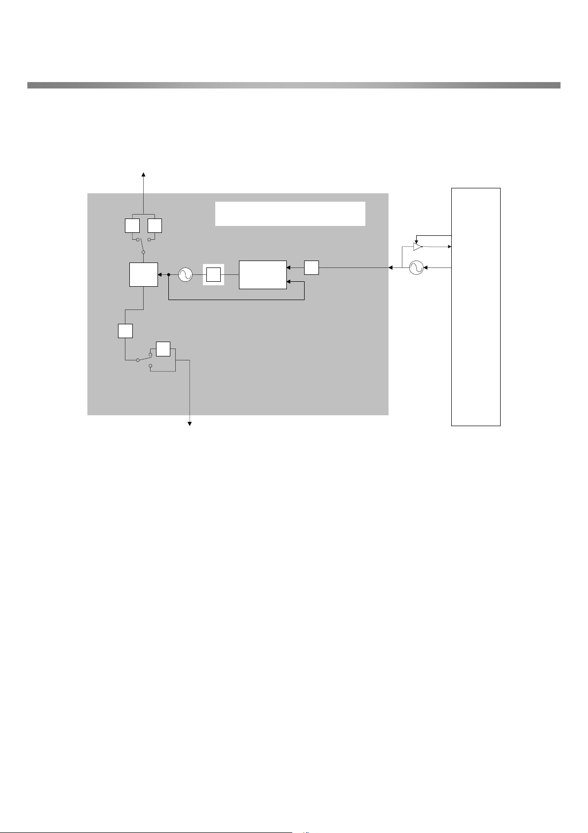
3.3 Transmitter Part
The Transmitter part contains CX74017 active parts, PAM and Antenna Switch. The CX74017 active part
consists of a vector modulator and offset phase-locked loop block(OPLL) including down-converter,
phase detector, loop filter and dual band transmit VCO which can operate at either final RF output
frequency. The RF GMSK outputs from the transmit VCO are fed directly to the RF power amplifiers.
GSMSEL
ANT
LMSP54AA-097
S/W
GSM : 880 ~ 925MHz
DCS : 1710 ~ 1785MHz
DCSSEL
PAM(RF3110B)
TXRAMP
TXPA
BANDSEL1
vco
f
LO
f
X2
CX74017
IF
f
Base
/3
X2
DCS
GSM
TX
f
Band
Block
TXVCO
/D1
PFD
LF
/D2
0
90
TXIP
TXIN
TXQP
TXQN
Fig.3-2 Transmitter Block diagram
The peak output power and the profile of the transmitted burst are controlled by means of power control
loop. The power control function is integrated, eliminating the need for directional couplers, detector
diodes, power control IC and other power control circuitry. This allows the module to be driven directly
from the DAC output. The PA outputs from the directional coupler pass to the antenna connector via
Antenna Switch.
A. IF Modulator
The baseband converter(BBC) within the GSM chipset generates I and Q baseband signals for the
transmit vector modulator. The modulator provides more than 40dBc of carrier and unwanted side-band
rejection and produces a GMSK modulated signal. The baseband software is able to cancel out
differential DC offsets in the I/Q baseband signals caused by imperfections in the D/A converters.
The TX-Modulator implements a quadrature modulator. The IF-frequency input signal is split into two
precise orthogonal carriers, which are multiplied by the baseband modulation signal IT/ITX and QT/QTX.
It is used as reference signal for the OPLL.
- 19 -

3. TECHNICAL BRIEF
B. OPLL
The offset mixer down converts the feedback Tx RF signal using LO to generate a IF modulating signal.
The IF signal goes via external passive bandpass filter to one port of the phase detector. The other side
of the phase detector input is LO signal. The phase detector generates an error current proportional to the
phase difference between the modulated signal from the offset mixer and the reference signal from the
LO.
The error current is filtered by a second order low-pass filter to generate an output voltage which depends
on the GMSK modulation and the desired channel frequency. This voltage controls the transmit VCO
such that the VCO output signal, centered on the correct RF channel, is frequency modulated with the
original GMSK data. The OPLL acts as a tracking narrowband band pass filter tuned to the desired
channel frequency. This reduces the wideband noise floor of the modulation and up-conversion process
and provides significant filtering of spurious products.
C. Synthesizer Part
The CX74017 includes a fully integrated UHF VCO with an on-chip LC tank.
A single sigma-delta fractional-N synthesizer can phase lock the local osillator used in both transmit
and receive path to a precision frequency reference input. Fractional-N operation offers low phase
noise and fast setting times, allowing for multiple slot applications such as GPRS.
The generated frequency is given by the following equation.
FN
++
f
ref
22
2
R
f
=
VCO
where : = Generated VCO frequency
f
VCO
N = N-divider ratio integer part
FN = Fractional setting
R = R-divider ratio
f
VCO
= Reference Frequency
N
5.3
- 20 -
3. TECHNICAL BRIEF
The counter and mode settings of the synthesizer are also programmed via 3-wire interface.
4/3 2/3
DCS
/3
DCS
GSM
CX74017
2V7_VTCXO
GSM
f
vco
X2
f
vco = (N+3.5+FN/2^22)fref/R
LF
f
LO
Fractional-N
PLL
f
ref
/R
13MHz
Figure 3-3. Synthesizer Block diagram.
13MHz
AFC
REFCLK
Base
Band
Block
D. Power Amplifier Module
The RF3110B[U416] is a Dual band amplifier for E-GSM(880 to 915MHz) and DCS1800(1710 to
1785MHz). The efficiency of module is the 50% at nominal output power for E-GSM and the 45% for DCS
1800. This module should be operated under the GSM burst pulse. To avoid permanent degradation,
CW operation should not be applied. To avoid the oscillation at no input power, before the input is cut off,
the control voltage Vapc should be control to less than 0.5V.
We have to improve thermal resistance, the through holes should be layouted as many as possible on
PCB under the module. And to get good stability, all the GND terminals should be soldered to ground
plane of PCB.
- 21 -
3. TECHNICAL BRIEF
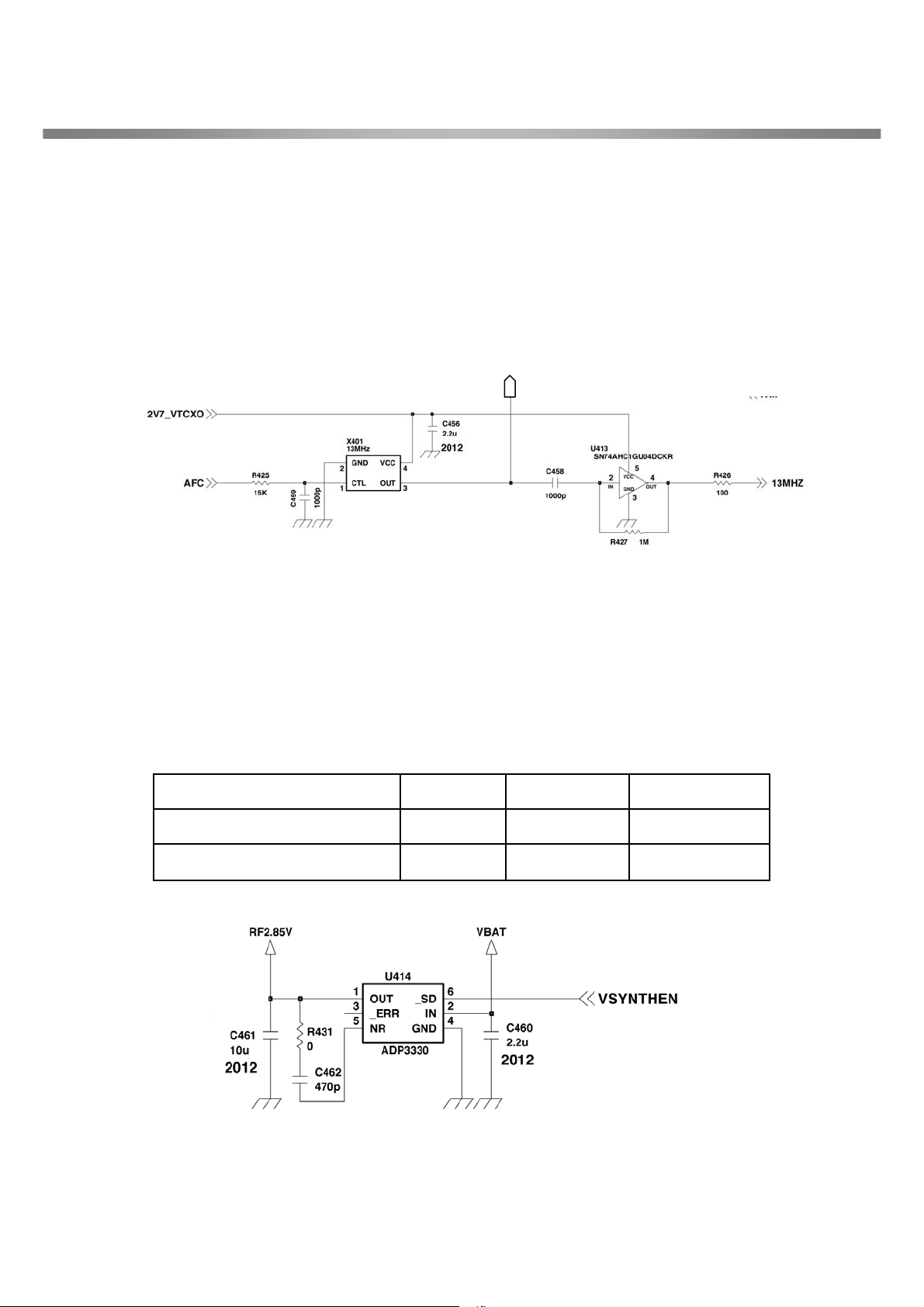
3.4 13 MHz Clock
The 13 MHz clock (VC-TCXO-208C) consists of a TCXO (Temperature Compensated Crystal Oscillator)
which oscillates at a frequency of 13 MHz.
It is used within the CX74017 RF Main Chip, BB Analog chip-set (AD6521), and Digital (AD6522).
FREF
Figure 3-4. VCTCXO Circuit.
3.5 Power Supplies for RF Circuits
There are two regulators used in the phone to provide RF power. One is contained inside of ADP3408
(U101), power management IC to provide the power for the VCTXO (X401). The other is used to
provide the power for remaining RF circuits.
Enable SignalPowersVoltageRegulator
VCTCXO2.7V± 0.5VRegulator 1(U101,2V7_VTCXO)
VSYNTHENRF circuitry2.85V± 0.5VRegulator 2 (U414,RF2V8)
Figure 3-5. Regulator Circuit.
- 22 -

3. TECHNICAL BRIEF
3.6 Testing Set-up and Checking Signals
A. Received RF Level and Checks
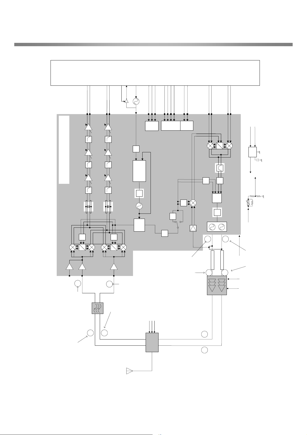
This section shows the typical RF power levels expected throughout the receiver path. A block diagram
shows the locations of the RF measurement points and levels as shown in Fig. 3-11.
Receiver Testing Set-up
To check the receiver the following conditions have to be set:
On a signal generator or a GSM/DCS test box, output amplitude of CW sugnal = -60 dBm at either:
947.4 MHz (CH62) when testing the GSM RX path or 1842.6 MHz (CH699) when testing the DCS
RX path. Set the DC power supply to 4.0 V.
Note: All RF values shown are only intended as a guide figure and may differ from readings taken
with other test equipment and leads. Lead and connector losses should always be taken into
account when performing such RF measurements.
Testing Receiver
Using a suitable high frequency probe measure the RF levels at the relevant points shown in Fig. 3-9
and compare your measurements with those shown in the diagram. If there are any major difference
between the readings taken and those indicated then further investigation of that particular point will be
required. It will also be necessary to ensure that all the following power supplies and signals are
present which control this part of the receiver circuit:
1. The Control Signal of FEM (see Fig. 3-15, 16, 17)
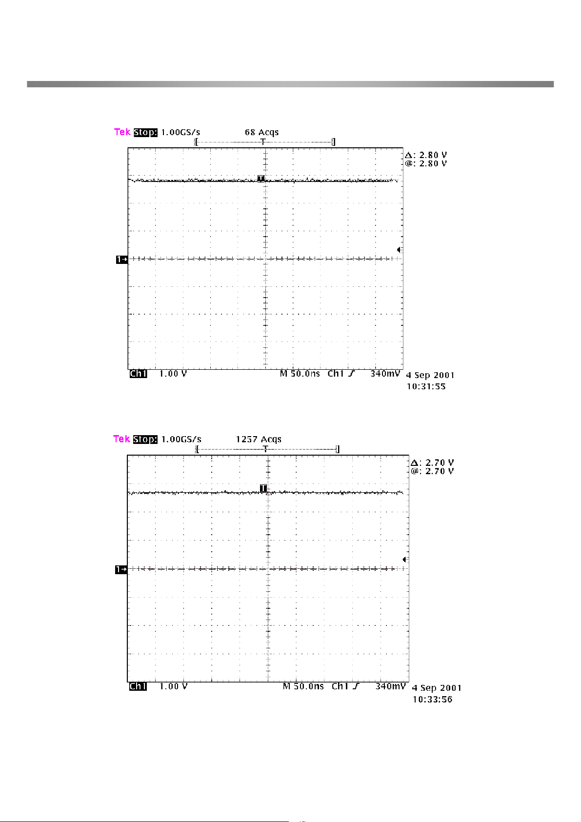
2. RF2V8 (see Fig. 3-12)
3. 2V7_VTCXO (see Fig. 3-13)
4. 13MHz (see Fig. 3-14)
5. CLK, DATA, SEN (see Fig. 3-18)
8. RX IP, IN, QP, QN (see Fig. 3-21)
B. Transmitted RF Power Level and Checks
This section shows the typical RF power levels expected throughout the transmitter path. A block
diagram shows the locations of the RF measurement points and levels as shown in Fig. 3-8.
Transmitter Testing Set-up
To check the transmitter the following conditions have to be set:
1. Set the DC Power supply to 4.0 V.
2. Power up the GSM/DCS test set and then establishing a call with an attached mobile on active
mode.
3. Select Channel, TX Level and Input Level according to which parameter is required.
Note: All RF values shown are only intended as a guide figure and may differ from readings taken with
other test equipment and leads. Lead and connector losses should always be taken into account when
performing such RF measurements.
- 23 -

3. TECHNICAL BRIEF
Testing Transmitter
Using a suitable high frequency probe measure the RF levels at the relevant points shown in Fig. 3-9,
10. and compare your measurements with those shown in the diagram. If there are any major
difference between the readings taken and those indicated then further investigation of that particular
point will be required. It will also be necessary to ensure that all the following power supplies and
signals are present which control this part of the transmitter circuit:
1. The Control Signal of FEM (see Fig. 3-15, 16, 17)
2. RF2V8 (see Fig. 3-12)
3. 2V7_VTCXO (see Fig. 3-13)
4. 13 MHz (see Fig. 3-14)
5. TXEN, TXRAMP, TXPA (see Fig. 3-19)
6. TX IP, IN, QP, QN (see Fig. 3-20)
- 24 -
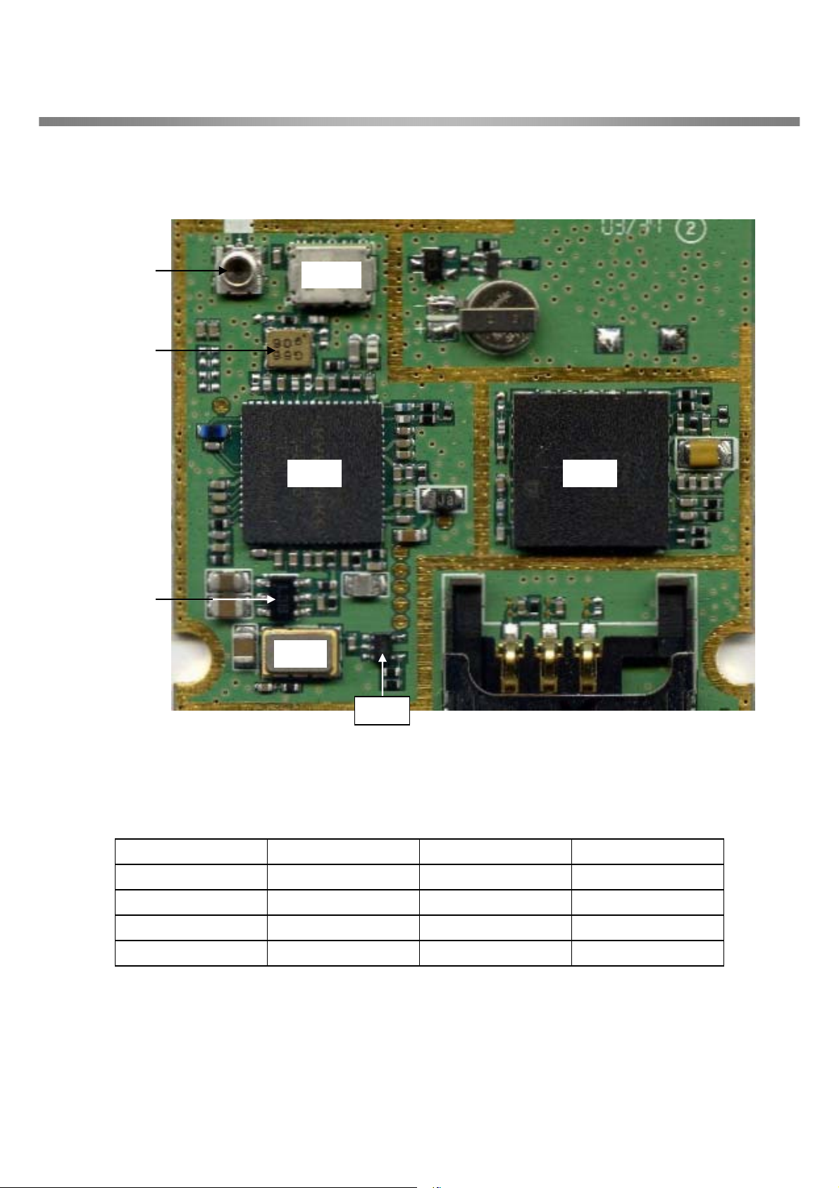
RF components (Component Side)
3. TECHNICAL BRIEF
CN303
FL406
U414
FL407
U441 U416
X401
U413
Figure 3-6. RF components (Component Side).
Reference Description Reference Description
U441 RF Main Chipset FL406 Dual SAW Filter
CN303 Mobile S/W X401 VCTCXO
FL407 Ant. S/W U414 LDO
U416 PAM U413 Inverter IC
- 25 -
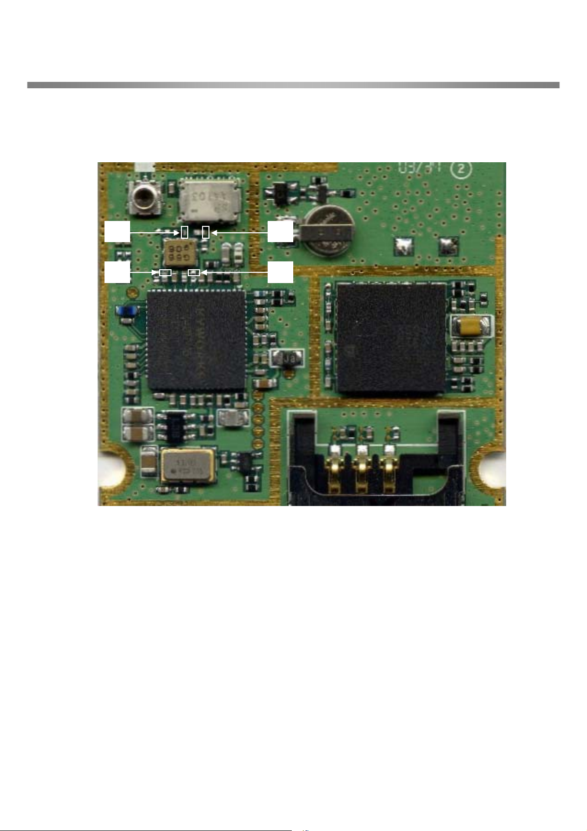
3. TECHNICAL BRIEF
Test point of Rx Levels
①
③
②
④
Figure 3-7. Test point of Rx Power Levels.
- 26 -
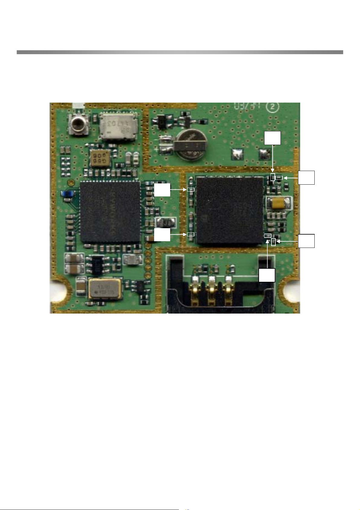
Test point of Tx Power Levels
3. TECHNICAL BRIEF
⑤
⑥
⑨
⑩
Figure 3-8. Test point of Tx Power Levels.
⑦
⑧
- 27 -
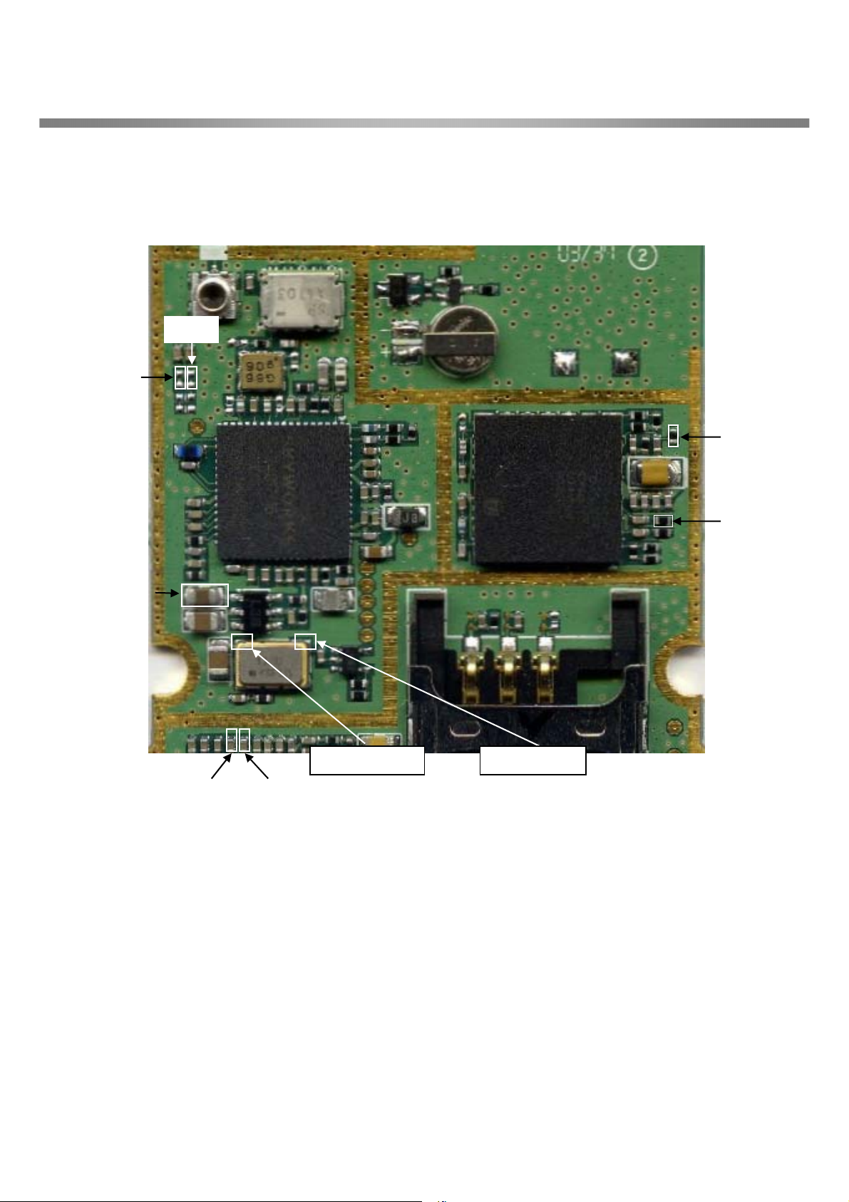
3. TECHNICAL BRIEF
Test point of Tx Power Levels
C444
C448
TXRAMP
(R401)
RF2.85V
TXQN TXIN
TXQP TXIP
TXPA
(R404)
2V7_VCTCXO 13MHz Clock
RXIN RXQN
RXIP RXQP
Figure 3-9. Control signal test points
- 28 -
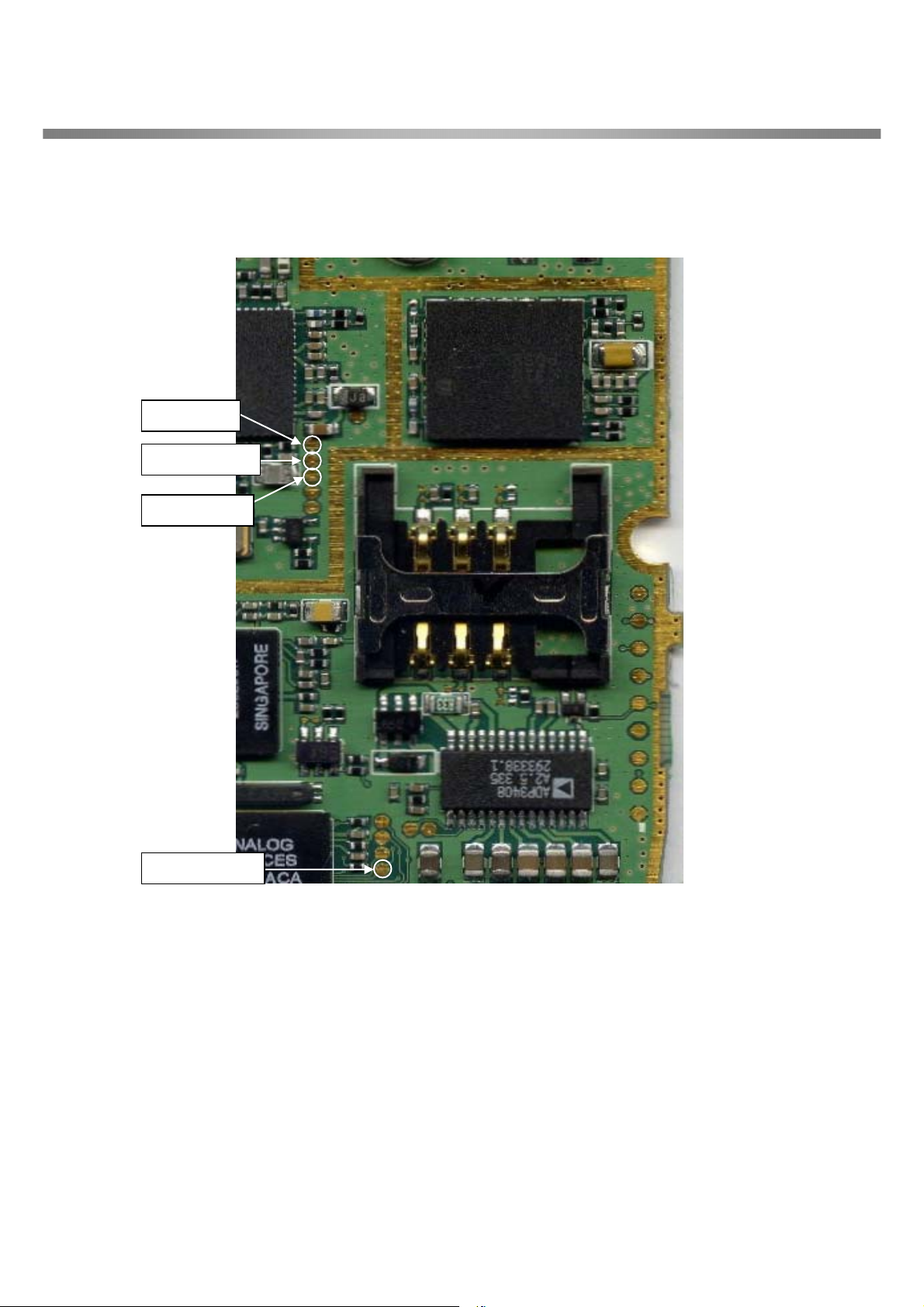
Control signal test points
TP402(LE)
TP404(Clock)
TP406(Data)
3. TECHNICAL BRIEF
TP403(RXEN)
Figure 3-10. Control signal test points
- 29 -
3. TECHNICAL BRIEF
RXIP
RXIN
CX74017
4/3
90
0
3
Base
Band
Block
AFC
13MHz
2V7_VTCXO
RXQP
RXQN
2/3
90
0
REFCLK
TXIP
PLL_LE
PLL_CLK
PLL_DATA
13MHz
I/O
Serial
ref
f
/R
ref/R
f
PLL
Fractional-N
vco = (N+3.5+FN/2^22)
f
LF
vco
f
TXEN
RXEN
FEENA
PLL_PD
I/O
Serial
/3
BANDSEL2
BANDSEL1
IF
f
LO
f
X2
X2
GSM
DCS
TX
f
TXIN
/D1
5
10 dBm
7
TXQP
TXQN
VBAT
VSYNTHEN
90
0
/D2
PFD
LF
TXVCO
/SD
OUT Vin
ADP3330_2V85
RF2.85V
TEMPSENSE
RF2.85V
6
8 dBm
Attanuator
Attanuator
TXEN
8
6 dBm
8 dBm
4
-64 dBm
PAM(RF3110B)
TXRAMP
-64.5 dBm
-61 dBm
-61 dBm
Dual Saw Filter L257
1
2
GSM
925 ~ 960MHz
GSMSEL
TXPA
DCSSEL
ANT
LMSP54AA-097
S/W
DCS
1805~1880MHz
-60 dBm
Figure 3-9. Transmitter & Receiver RF Levels
- 30 -
9
34 dBm32 dBm
10
GSM : 880~925MHz
DCS : 1710 ~ 1785MHz
3. TECHNICAL BRIEF
Figure 3-12. Regulator Output (RF2V8)
Figure 3-13. VCTCXO Power Supply (2V7_VTCXO).
- 31 -
 Loading...