

LG FM300 Service Manual

Internal Use Only
Service Manual
FM300
Date: January, 2011 / Issue 1.0

- 2 -
Copyright © 2011 LG Electronics. Inc. All right reserved.
Only for training and service purposes
LGE Internal Use Only
Table Of Contents
1. INTRODUCTION ..................................................................... 3
1.1 Purpose ........................................................................................................3
1.2 Regulatory Information .........................................................................3
1.3 Abbreviations.............................................................................................5
2. PERFORMANCE ...................................................................... 8
2.1 H/W Features ..............................................................................................8
2.2 LTE Technical Specification (TS 36.101 v10.0.0)............................9
3. TECHNICAL BRIEF ................................................................12
3.1 MAIN ........................................................................................................... 12
3.2 LTE(SUB) .................................................................................................... 19
4. TROUBLE SHOOTING .......................................................... 24
4.1 Power on Trouble – 3.3V Main power ........................................... 24
4.2 Power on Trouble – BCM Booting Trouble .................................. 27
4.3 Power on Trouble – 3.75V LTE power ............................................31
4.4 SIM card Trouble .................................................................................... 35
4.5 Power LED Indication Trouble .......................................................... 41
4.6 Ethernet LED Indication Trouble ..................................................... 43
4.7 RGB LED Indication Trouble .............................................................. 45
4.8 USB Connection Trouble .................................................................... 47
4.9 Ethernet Connection Trouble ........................................................... 52
4.10 LTE RF Component (Primary) ......................................................... 55
4.11 LTE VCXO Trouble ................................................................................ 56
4.12 LTE Tx Trouble ....................................................................................... 58
4.13 Power on Trouble – LTE Booting Trouble .................................. 60
4.14 Memory Trouble shooting ..............................................................64
5. DOWNLOAD ......................................................................... 67
6. BLOCK DIAGRAM ................................................................. 73
7. CIRCUIT DIAGRAM ..............................................................74
8. BGA PIN MAP
......................................................................85
9. PCB LAYOUT ......................................................................... 86
10. CALIBRATION ..................................................................... 90
10.1 LTE AUTO CALIBRATION ...................................................................90
11. STAND ALONE TEST .......................................................... 97
11.1 Introduction .......................................................................................... 97
12. EXPLODED VIEW & REPLACEMENT PART LIST ............... 99
12.1 EXPLODED VIEW .................................................................................. 99
12.2 Replacement Parts ...........................................................................101
12.3 Accessory .............................................................................................128

- 3 -
Copyright © 2011 LG Electronics. Inc. All right reserved.
Only for training and service purposes
LGE Internal Use Only
1. INTRODUCTION
1. INTRODUCTION
1. INTRODUCTION
1.1 Purpose
This manual provides the information necessary to repair, calibration, description and download the features
of this model.
1.2 Regulatory Information
A. Security
Toll fraud, the unauthorized use of telecommunications system by an unauthorized part (for example, persons
other than your company’s employees, agents, subcontractors, or person working on your company’s behalf)
can result in substantial additional charges for your telecommunications services. System users are responsible
for the security of own system. There are may be risks of toll fraud associated with your telecommunications
system. System users are responsible for programming and configuring the equipment to prevent
unau
thorized use. The manufacturer does not warrant that this product is immune from the above case but
will prevent unauthorized use of common-carrier telecommunication service of facilities accessed through or
connected to it.
The manufacturer will not be responsible for any charges that result from such unauthorized use.
B. Incidence of Harm
If a telephone company determines that the equipment provided to customer is faulty and possibly causing
harm or interruption in service to the telephone network, it should disconnect telephone service until repair
can be done. A telephone company may temporarily disconnect service as long as repair is not done.
C. Changes in Service
A local telephone company may make changes in its communications facilities or procedure. If these changes
could reasonably be expected to affect the use of the this phone or compatibility with the network, the
telephone company is required to give advanced written notice to the user, allowing the user to take
appropriate steps to maintain telephone service.
D. Maintenance Limitations
Maintenance limitations on this model must be performed only by the manufacturer or its authorized agent.
The user may not make any changes and/or repairs expect as specifically noted in this manual. Therefore, note
that unauthorized alternations or repair may affect the regulatory status of the system and may void any
remaining warranty.
1. INTRODUCTION

- 4 -
Copyright © 2011 LG Electronics. Inc. All right reserved.
Only for training and service purposes
LGE Internal Use Only
1. INTRODUCTION
1. INTRODUCTION
E. Notice of Radiated Emissions
This model complies with rules regarding radiation and radio frequency emission as defined by local regulatory
agencies. In accordance with these agencies, you may be required to provide information such as the following
to the end user.
F. Interference and Attenuation
Phone may interfere with sensitive laboratory equipment, medical equipment, etc.Interference from
unsuppressed engines or electric motors may cause problems.
G. Electrostatic Sensitive Devices
ATTENTION
Boards, which contain Electrostatic Sensitive Device (ESD), are indicated by the sign.
Following information is ESD handling:
• Service personnel should ground themselves by using a wrist strap when exchange system boards.
• When repairs are made to a system board, they should spread the floor with anti-static mat which is also
grounded.
• Use a suitable, grounded soldering iron.
• Keep sensitive parts in these protective packages until these are used.
• When returning system boards or parts like EEPROM to the factory, use the protective package as described.

- 5 -
Copyright © 2011 LG Electronics. Inc. All right reserved.
Only for training and service purposes
LGE Internal Use Only
1. INTRODUCTION
1.3 Abbreviations
1. INTRODUCTION
For the purposes of this manual, following abbreviations apply:
Automatic Power ControlAPC
Adjacent Channel Selectivity ACS
Adjacent Channel Leakage Ratio ACLR
Bit Error RatioBER
BasebandBB
Additive White Gaussian Noise AWGN
Additional Maximum Power Reduction A-MPR
j y
Constant Current – Constant VoltageCC-CV
Base Station BS
Cyclic Prefix CP
dB relative to 1 milli wattdBm
Digital to Analog ConverterDAC
Continuous Wave CW
Downlink Control Information DCI
Digital Signal ProcessingDSP
Digital C
ommunication System
DCS
Downlink
DL
E-UTRA Absolute Radio Frequency Channel Number EARFCN
Electrostatic DischargeESD
Electrical Erasable Programmable Read
-
Only Memory
EEPROM
- 6 -
Copyright © 2011 LG Electronics. Inc. All right reserved.
Only for training and service purposes
LGE Internal Use Only
1. INTRODUCTION
1. INTRODUCTION
Error Vector Magnitude EVM
Evolved UMTS Terrestrial Radio Access Network EUTRAN
Evolved UMTS Terrestrial Radio Access E-UTRA
Energy Per Resource Element EPRE
General Purpose Interface BusGPIB
Gaussian Minimum Shift KeyingGMSK
Flexible Printed Circuit BoardFPCB
Frequency Division Duplex FDD
Liquid Crystal DisplayLCD
Intermediate FrequencyIF
International Portable User IdentityIPUI
Global System for Mobile Communications
GSM
Light Emitting DiodeLED
Low Drop Output
LDO
Modulation and Coding Scheme MCS
Orthogonal Frequency Division Multiple Access OFDMA
Offset Phase Locked Loop
OPLL
Phase Locked Loo
p
PLL
Programmable Gain AmplifierPGA
Printed Circuit BoardPCB
Power Amplifier ModulePAM
Public Switched Telephone NetworkPSTN
p

- 7 -
Copyright © 2011 LG Electronics. Inc. All right reserved.
Only for training and service purposes
LGE Internal Use Only
1. INTRODUCTION
1. INTRODUCTION
Radio FrequencyRF
Real Time ClockRTC
Root Mean SquareRMS
Receiving Loudness RatingRLR
Reference Signal RS
Static Random Access MemorySRAM
Sending Loudness RatingSLR
Subscriber Identity ModuleSIM
Surface Acoustic WaveSAW
Travel AdapterTA
Side Tone Masking RatingSTMR
Pseudo SRAMPSRAM
Signal-to-Noise Ratio SNR
Universal Asynchronous Receiver/TransmitterUART
Time Division Multiple AccessTDMA
Time Division DuplexTDD
User Equipment UE
Wireless Application Protocol
WAP
Voltage Control Temperature Compensated Crystal OscillatorVCTCXO
Voltage Controlled OscillatorVCO
Uplink UL
2. PERFORMANCE
- 8 -
Copyright © 2011 LG Electronics. Inc. All right reserved.
Only for training and service purposes
LGE Internal Use Only
2. PERFORMANCE
2.1 H/W Features
2. PERFORMANCE
Item Feature Comment
Standard Battery No: use external power adapter
Talk Current Under 450mA: LTE power 22.5dBm
Stand by Current Under 250mA: LTE network
Ch
arging time
N
o: use external power adapter
RX Sensitivity LTE: -101dBm(BW10MHz)
TX output power LTE:22.5dBm (class3)
SIM card type 8pin push-push type
Display No: LED indicators only
Power Indicator
Blinking white: Start up or new firmware is being
downloaded. Do not turn off or reboot the device
during the process.
Solid white: Normal operation
Off: Power off
Signal Indicator Red: Internet connection is not available. Weak
signal strength
Yellow: Internet connection is available. Medium
signal strength
Green: Internet connection is available. Strong
signal strength
ANT External
Ear phone jack No: only CPE
Speech coding No: only CPE
Vibrator No: only CPE
Loud Speaker No: only CPE
Microphone No: only CPE
Speaker/Receiver No: only CPE
T
ravel Adapter Yes: External power source
MIDI No: only CPE
2. PERFORMANCE
2. PERFORMANCE
- 9 -
Copyright © 2011 LG Electronics. Inc. All right reserved.
Only for training and service purposes
LGE Internal Use Only
2.2 LTE Technical Specification (TS 36.101 v10.0.0)
2. PERFORMANCE
ItemS
pec
ificati
on
Transmit Frequency
E-UTRA Band 20
832MHz ~ 862MHz
Maximum Output Power
+23 dBm , ·2 dB (class 3)
Frequency Error |Δf| ≤ (0.1 PPM + 15 Hz)
Open Loop Power Control
Normal Conditions : within ·9 dB,
Extreme Conditions : within ·12 dB
Minimum Output Power
< -40 dBm
Occupied Bandwidth
10 MHz
Channel Bandwidth 10 MHz
Adjacent Channel Leakage
Power Ratio (ACLR)
UTRAACLR1 33 dB
Adjacent channel center frequency offset
(in MHz)
+ / - 7.5 MHz
UTRA
ACLR2 36 dB
Adjacent channel center frequency offset
(in MHz)
+ / - 12.5 MHz
E-UTRA
ACLR 30 dB
Adjacent channel center frequency offset
(in MHz)
+ / - 10 MHz
E-UTRA channel Measurement bandwidth 9 MHz
UTRA 5MHz channel Measurement
bandwidth
3.84 MHz
BW Channel 10 MHz
Transmit Intermodulation
Interference Signal Frequency Offset
10 MHz
20MHz
Interference CW Signal Level - 40 dBc
Intermodulation Product -29 dBc -35 dBc
Measured Bandwidth 9 MHz 9 MHz
2. PERFORMANCE
- 10 -
Copyright © 2011 LG Electronics. Inc. All right reserved.
Only for training and service purposes
LGE Internal Use Only
2. PERFORMANCE
Item
Specification
Error Vector Magnitude
< 17.5 %, when Pout ≥ -40 dBm (for BPSK or QPSK)
< 12.5 %, when Pout ≥ -40 dBm (for 16QAM)
EVM equalizer Spectrum
Flatness
If FUL_measurement - FUL_low ≥ 3MHz
and
If FUL_high - FUL_measurement ≥ 3 MHz
Æ+2/-2 dB
If FUL_measurement - FUL_low < 3 MHz
or
If FUL_high - FUL_measurement < 3 MHz
Æ+3/-5 dB
ΔfOOB boundary between E-UTRA channel and spurious emission
domain for 10 MHz channel bandwidth = 15 MHz
Frequency Range Maximum Level
Measurement
Bandwidth
Transmitter Spurious
Emission
9 kHz d f < 150 kHz
-36 dBm 1 kHz
150 kHz d f < 30 MHz
-36 dBm 10 kHz
30 MHz d f < 1000 MHz
-36 dBm 100 kHz
1 GHz d f < 12.75 GHz
-30 dBm 1 MHz
2. PERFORMANCE
- 11 -
Copyright © 2011 LG Electronics. Inc. All right reserved.
Only for training and service purposes
LGE Internal Use Only
2. PERFORMANCE
ItemS
pec
ificati
on
Receive Frequency
E-UTRA Band 20
792MHz ~ 822MHz
Reference Sensitivity Level Maximum throughput >=95% when Î
or
= -94 dBm / 10 MHz (Single)
Maximum throughput >=95% when Î
or
= -97 dBm / 10 MHz (Dual)
M
a
ximum In
put Leve
l Maximum thr
oughput
>=
95%
when Î
= -25 dBm
(at each antenna port)
a u put e e
a u t oug put 95% e
or
5dB(at eac a te a po t)
Adjacent Channel Selectivity
(ACS)
ACS > 33 dB where Maximum throughput >=95%
for Channel BW = 10MHz
Adjacent Channel Interferer(ACI) frequency offset = ·7.5MHz
ACI BW = 5MHz
Spurious Response Maximum throughput >=95%
-
when
Îor= refsens
+ 6 dBm
& I
blocki
ng
= 44 dBm
Intermodulation Maximum throughput >=95%
when Î
or
= refsens + 6dBm
& P
interferer1
= -46 dBm /5MHz @ F
interferer1
(offset) = ·12.5 MHz
& P
interferer2
= -46 dBm /5MHz @ F
interferer2
(offset) = ·25 MHz
Spurious Emissions < -57 dBm / 100 kHz @ 30MHz ≤ f < 1 GHz
< -47 dBm/ 1 MHz @ 1 GHz ≤ f ≤ 12.75 GHz
3. TECHNICAL BRIEF
- 12 -
Copyright © 2011 LG Electronics. Inc. All right reserved.
Only for training and service purposes
LGE Internal Use Only
3. TECHNICAL BRIEF
3. TECHNICAL BRIEF
The Broadcom® BCM5358U processor is the highest performance chip in the Intensi-fi® XLR processor family.
Integrating a powerful 533 MHz MIPS32® 74KTM core with a four-way set associative 32 KB instruction cache,
a 2-way set associative 32 KB data cache, and a 64-entry TLB, the BCM5358U offers significant performance
improvements in both transfer rates and CPU utilization.
3.1 MAIN
3.1.1 Network Processor (BCM5358U, U200)
Flexible support for a variety of system bus interfaces is provided, including one USB 2.0 EHCI (OHCI 1.0 support)
host port, one USB HSIC port , 16-bit DDR400 memory control, serial Flash port . There are shared GPIOs with
other functions on the BCM5358U processor. All inputs can be used to generate processor interrupts. The
sections below describe each major functional block in more detail.
The BCM5358U has a 5-port, non-blocking 10/100 Ethernet switch. Any of the five ports can be configured as
the WAN port, with the other four being LAN ports. Each port can be programmed to support four-level priority
queues for quality of service (IEEE 802.1p QoS). IEEE 802.1q VLAN, IGMP snooping, and IP DiffServ/ToS are also
™
supported. The MAC is IEEE 802.3u compliant and supports a frame size up to 1536 bytes.
General:
• IEEE 802.11n-compliant.
• Integrated 2.4 GHz radio.
• Internal PAs capable of Pout > 18 dBm (G band).
• Simultaneous dual-band support with additional MAC/PHY/Radio (e.g., BCM43236).
• 2-stream spatial multiplexing up to 200 Mbps.
• Supports 2 Ý 2 and optional diversity with 3 antennas.
• Supports MCS 0 – 15 and MCS 32 modulation and coding rates in 802.11n.
• Supports 20 MHz and 40 MHz channels with optional SGI.
• Support for STBC in both TX and RX.
• Full IEEE 802.11b/g legacy compatibility with enhanced performance.
• Advanced MIPS32® 74KTM Core:
- 32 KB I-cache, 32 KB D-cache
- CPU can run up to 533 MHz/960 DMIPs
• MMU/TLB support for Linux®.
• Five-port integrated 10/100BASE-TX IEEE 802.3u™ compliant Auto-MDIX transceivers and LAN/WAN switch
controller.
• Advanced Ethernet MAC (BCM5358 only):
- MII PHY interface.
- Supports external 10/100 switch, such as the BCM5325E.
• One USB 2.0 host port plus one 480 MHz HSIC port
• 16-bit DDR400 su
pp
ort up to 2 Gbit capacity.
pp p p y
• Supports serial Flash up to 16 MB.
• UART and JTAG interface, up to 32 GPIOs.
• BCM5358U package: 15 mm Ý 15 mm 366-pin TFBGA
3. TECHNICAL BRIEF
3. TECHNICAL BRIEF
- 13 -
Copyright © 2011 LG Electronics. Inc. All right reserved.
Only for training and service purposes
LGE Internal Use Only
3. TECHNICAL BRIEF
3.1.2 DDR1 Memory (MT46V16M16P-6TIT, U201)
T
he MT46V16M16P-6TIT is a 256Mb Double Data Rate(DDR) SDRAM. The DDR SDRAM uses a double data rate
architecture to achieve high-speed operation. The double data rate architecture is essentially a 2n-prefetch
architecture with an interface designed to transfer two data words per clock cycle at the I/O pins. A single read or
write access for the DDR SDRAM effectively consists of a single 2n-bit-wide, one-clockcycle
data transfer at the internal DRAM core and two corresponding n-bit-wide, onehalf-clock-cycle data transfers at
the I/O pins.
•
VDD = +2.5V
·
0.2V, VDDQ = +2.5V
·
0.2V
• VDD = +2.6V ·0.1V, VDDQ = +2.6V ·0.1V (DDR400)
• Bidirectional data strobe (DQS) transmitted/received with data, that is, source-synchronous data capture
(x16 has two – one per byte)
• Internal, pipelined double-data-rate (DDR) architecture; two data accesses per clock cycle
• Differential clock inputs (CK and CK#)
• Commands entered on each positive CK edge
• DQS edge-aligned with data for READs; centeraligned with data for WRITEs
•
DLL t
o align DQ and
DQS t
rans
iti
ons w
ith CK
• Four internal banks for concurrent operation
• Data mask (DM) for masking write data (x16 has two – one per byte)
• Programmable burst lengths (BL): 2, 4, or 8
• Auto refresh
– 64ms, 8192-cycle(Commercial & Industrial)
– 16ms, 8192-cycle (Automotive)
• Self refresh (not available on AT devices)
• Longer-lead
TSOP f
or improved relia
bili
ty
(OCPL)
• 2.5V I/O (SSTL_2-compatible)
• Concurrent auto precharge option supported
• 66-pin TSOP (Pb-free) (22.22mm x 11.76mm x 1.2mm)
CKE
CK#
DQ0-DQ15
256Mb
DDR1 SDRAM
Memory
CK
CS#
WE#
CAS#
RAS#
A0-A12
LDQS
UDQS
LDM
UDM
Figure 3.2 MT46V16M16P-6TIT Block Diagram
BA0,BA1
3. TECHNICAL BRIEF
- 14 -
Copyright © 2011 LG Electronics. Inc. All right reserved.
Only for training and service purposes
LGE Internal Use Only
3. TECHNICAL BRIEF
3.1.3 Serial Flash (N25Q128, U202)
T
he N25Q128 is a 128 Mbit (16Mb x 8) serial Flash memory, with advanced write protection mechanisms.
It is accessed by a high speed SPI-compatible bus and features the possibility to work in XIP (“eXecution in
Place”) mode.
The N25Q128 supports innovative, high-performance quad/dual I/O instructions, these new instructions allow
to double or quadruple the transfer bandwidth for read and program operations.
• SPI-compatible serial bus interface
•
108 MHz (
maximum) clock frequency
• 2.7 V to 3.6 V single supply voltage
• Supports legacy SPI protocol and new Quad I/O or Dual I/O SPI protocol
• Quad/Dual I/O instructions resulting in an equivalent clock frequency up to 432 MHz:
• XIP mode for all three protocols
– Configurable via volatile or non-volatile registers (enabling the memory to work in XiP mode directly after
power on)
• Program/Erase suspend instructions
• Continuous read of entire memory via single instruction:
– Fast Read
– Quad or Dual Output Fast Read
– Quad or Dual I/O Fast Read
• Flexible to fit application:
– Configurable number of dummy cycles
– Output buffer configurable
– Fast POR instruction to speed up power on phase
– Reset function available upon customer Request
• 64-byte user-lockable, one-time programmable (OTP) area
• Packages VDFPN8(F8) 8 x 6 mm(MLP8)
Figure 3.3 N25Q128 Block Diagram
3. TECHNICAL BRIEF
- 15 -
Copyright © 2011 LG Electronics. Inc. All right reserved.
Only for training and service purposes
LGE Internal Use Only
3. TECHNICAL BRIEF
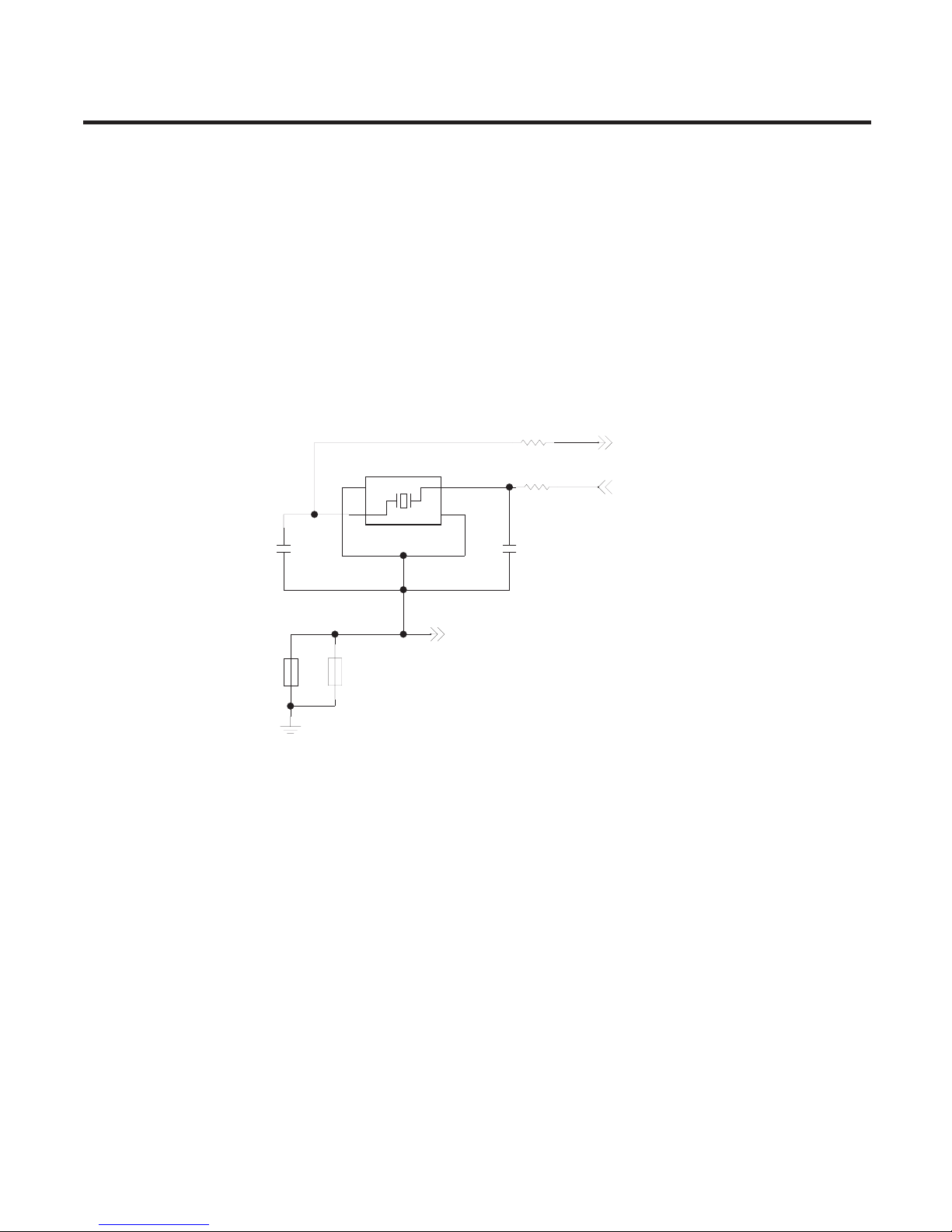
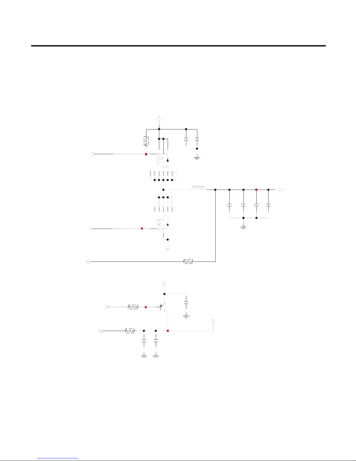
3.1.4 20 MHz Clock (Crystal, X400)
For the generation of the reference frequency for BCM5358U an external Crystal unit is used.
The XTAL ground is separated from main ground for reducing noise. It is used for the various clocks,
including the clock for the 10/100 MAC core (25 MHz) and the MIPS32 74K, UART, and USB 2.0 host in
BCM5358U.
Figure 3.4 Crystal Circuit diagram
600
FB400
220
R407
0R406
33p
C422
33p
C423
20MHz
CXC3X200000GHVRG00
EXXY0027801
X400
4
2
3
1
HOT1
HOT2
GND1
GND2
600
FB401
XTAL_OUT
XTAL_IN
XTAL_GND
GND
20MHz CRYSTAL
3. TECHNICAL BRIEF
- 16 -
Copyright © 2011 LG Electronics. Inc. All right reserved.
Only for training and service purposes
LGE Internal Use Only
3. TECHNICAL BRIEF
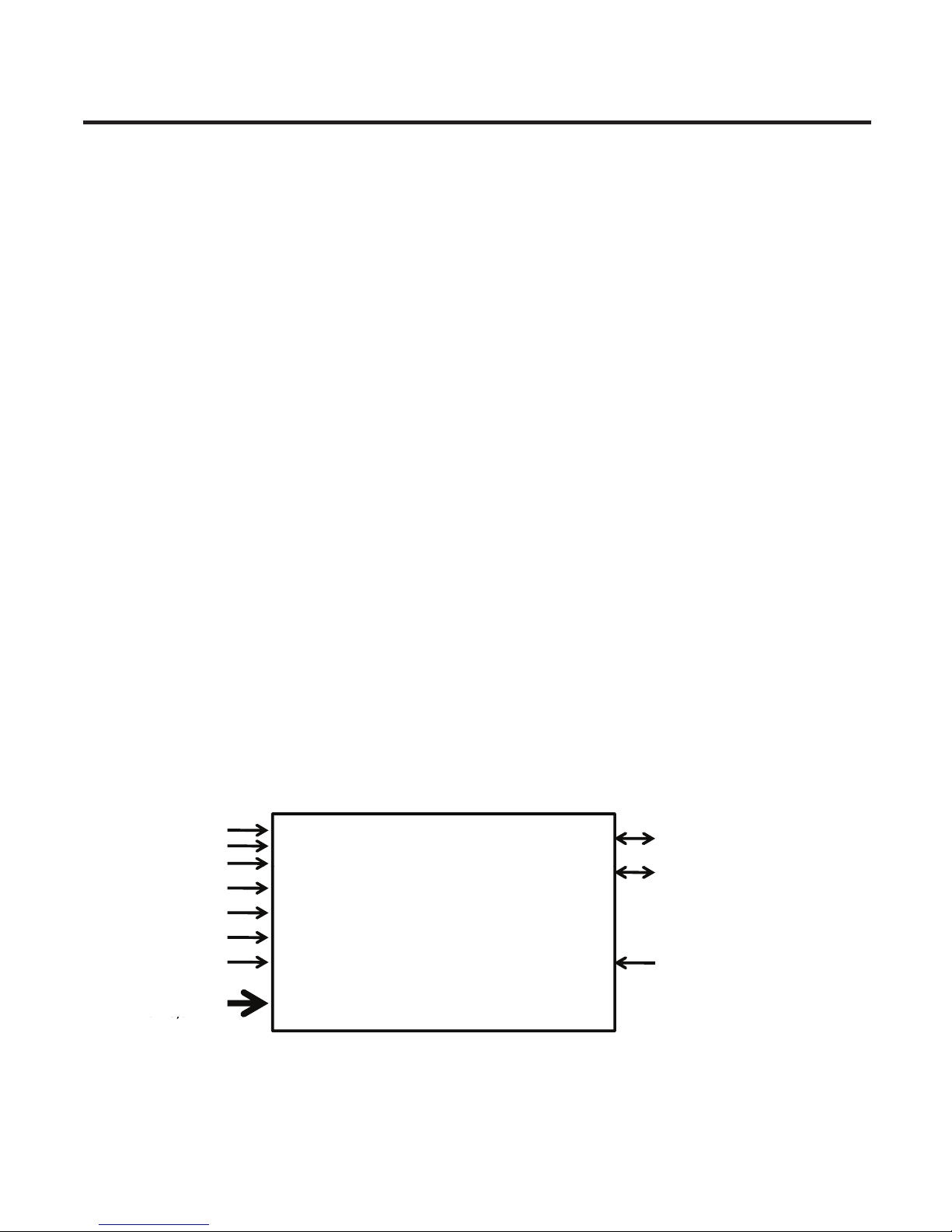
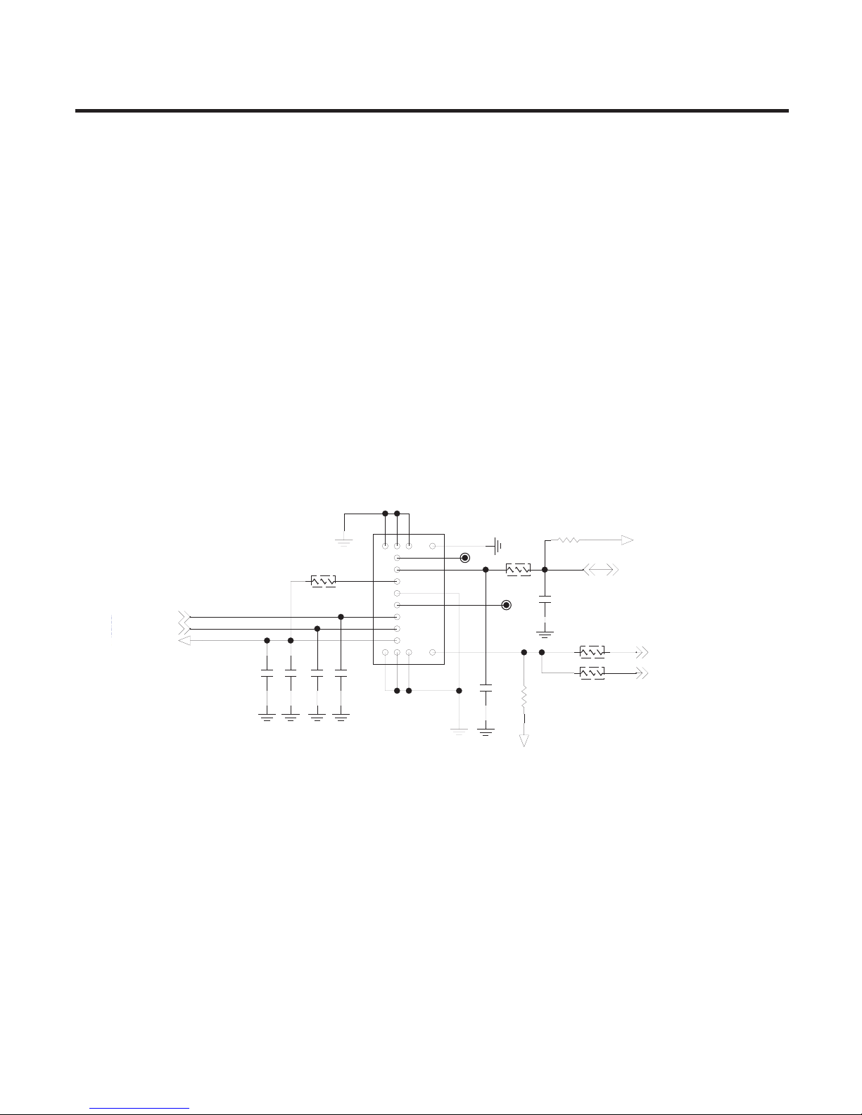
3.1.5 SIM Interface (S300)
This SIM interface is placed in main board, but is connected with LTE module. Also it is controlled and
detected from LTE module. It is the push-push type SIM socket. SIM interface scheme is shown in figure.
SIM Interface
SIM_CLK : SIM card reference clock
SIM_RST : SIM card Async /sync reset
SIM_DATA : SIM card data
SIM_PWR : SIM card power source
LTE_USIM_DET/ : SIM card detection to LTE Module
NP_USIM_DET/ : SIM card detection to BCM5358U ( It is optional. Not used )
Figure 3.5 SIM
0.1u
C339
R350 0
60
3R
K1
TP302
TP303
DNIR351
100p
C340
33p
C341
33p
C342
4.7K
R348
SIM_PWR
S300
ENSY0023001
SCGC1B0100
1
2
3
4
5
6
7
8
G5 G3 G1
COMMON
G6 G4 G2
SW
DNI
C350
VDD_3.3
0R308
SIM_PWR
R307 0
DNI
C349
NP_USIM_DET/
LTE_USIM_DET
/
SIM_RST/
SIM_CLK
SIM_DATA
3. TECHNICAL BRIEF
- 17 -
Copyright © 2011 LG Electronics. Inc. All right reserved.
Only for training and service purposes
LGE Internal Use Only
3. TECHNICAL BRIEF
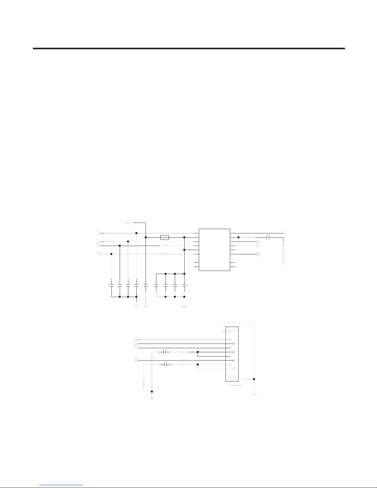
3.1.6 Ethernet Interface (Transformer & RJ-45, U104 & CN101)
This Ethernet Interface is connected to the outside device through the RJ-45 connecter.
And the Ethernet signals from the connecter go into the transformer with the function which is line impedance
matching of Ethernet port.
This transformed impedance required the differential 100ohm for the Main chipset (BCM5358U).
The Ethernet signals go from the transformer to BCM5358U which is the Main chipset.
Ethernet Interface
PORT1_TDP : Plus signal of Ethernet transmit pair.
PORT1_TDN : Minus signal of Ethernet transmit pair.
PORT1_RDP : Plus signal of Ethernet receive pair.
PORT1_RDN : Minus signal of Ethernet receive pair.
Figure 3.6 Transformer & RJ-45
220FB100
8.2p
C153
8.2p
C154
8.2p
C151
8.2p
C152
0.1u
C132
0.1u
C131
0.1u
C128
75R134
0
631R
VDD_2.5
10u
C130
10u
C129
0R138
0R137
0R135
C127 1n
0R133
U104
ELCP0009412
TLA-6T118LF
14
16
12
10
1
8 9
13
116
7
5
4
3
2 15
CM2V_CTR1
TD-
NC1
NC2
V_CTR2
RD+ RX+
NC4
RX-RD-
TD+
CM1
NC3
TX+
TX-
PORT1_RDN
PORT1_RDP
PORT1_TDN
PORT1_TDP
P1_RDP
P1_RDN
P1_TDP
P1_TDN
C137 1n
C138 1n
CN101
ENZY0030801
85507-5001
10
8
4
7
3
6
2
5
1
9
G1G4G3
G2
0
0
51
R
0
15
1
R
75R148
75R146
P1_RDP
P1_RDN
P1_TDP
P1_TDN
3. TECHNICAL BRIEF
- 18 -
Copyright © 2011 LG Electronics. Inc. All right reserved.
Only for training and service purposes
LGE Internal Use Only
3. TECHNICAL BRIEF
3.1.7 Buck Convertor (SC424, U1&2)
We use two SC424. U2 is for BCM5358U and U1 is for LTE Module. U2 output voltage is set to 3.3V and U1 output
voltage is set to 3.75V. The current limit setting is 2.16A same. We use 12V main power source from Adaptor.
The SC424 convert down from 12V to 3.3V and 3.75V for all circuit applications.
Figure 3.7 SC424 Circuit Diagram
C3
1u
C8
2.2u
C9
10n
2R
K1.91
C12
47p
C1
DNI
SPPH410100
4
3
5
261
2
0
1NC
ESPY0001701
C4 1u
R7 2.7K
01R
K74
U2
EUSY0369702
SC424
3
31
6
1
30
32
729262
22
01
52
15
31
16
20
19
82
41
21
8
9
7
2
42
2
1
5
18
11
174
VOUT PGND4
4NIV
PGND5
VIN
TSBXL
SXL
V5V
BST
2NIV
1N
IV
LX3
2DNGP
LNE
PGND6
LX2
PGND3
1DNGP
LX1
VSP
/NE
3NIV
DOOGP
2DNGA
3DNGA
NOT
MILI
VIN5
FB
VLDO
LX4
AGND1
R11 100K
C18
100n
100n
C19
SC424
EUSY0369702
U1
3
31
6
1
30
32
729262
22
0
1
5
2
15
3
1
16
20
19
82
4
1
21
8
9
7
2
42
21
5
18
11
174
VOUT PGND4
4
NIV
PGND5
VIN
TSBXL
SX
L
V5V
BST
2NIV
1NIV
LX3
2DNGP
LNE
PGND6
LX2
PGND3
1DNGP
LX1
VSP/NE
3NIV
DOOGP
2DNGA
3D
NGA
N
OT
MILI
VIN5
FB
VLDO
LX4
AGND1
K74
9R
1uC5
DNI
C2
47p
C11
K1.91
1
R
10n
C10
2.2u
C7
1u
C6
C115
DNI
KRX102U
EQBA0000601
1
0
1
Q
5
4
1 2
3
04
21
R
3
21
R
K
0
1
C126
DNI
L100
2.2u
2.2u
L101
100KR12
DNIR13
R14 100K
VA100
5
1R
K0
21
LD100
EDLM0009901
67-21-L9C-W4556W1X1B2-2T
C15
10u
VDD_3.75
0.1u
C103
VDD_3.3
R8 2.7K
0.1u
C121
C104
22u
IND011R
DNI
C110
C119
22u
5
R
K
03
DNI
C116
C14
10u
551R I
N
D
6
R
K61
3
R
K65
R102 100K
R104
10
100KR103
1K
R114 Q100
EQBN0005301
UMT2222A
1
2
3
C120
22u
C101
22u
C105
22u
10u
C13
C102
22u
PWR_LED
LTE_PWR_EN
NP_EN
LTE_EN
Power LED(White)
FOR N.P POWER [3.3V/2.16A]
FOR LTE MODULE POWER [3.75V/2.16A]
3. TECHNICAL BRIEF
- 19 -
Copyright © 2011 LG Electronics. Inc. All right reserved.
Only for training and service purposes
LGE Internal Use Only
3. TECHNICAL BRIEF
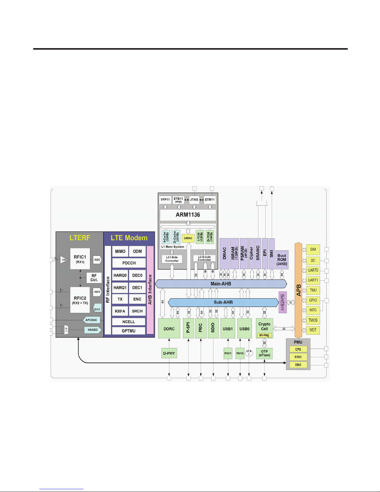
3.2 LTE(SUB)
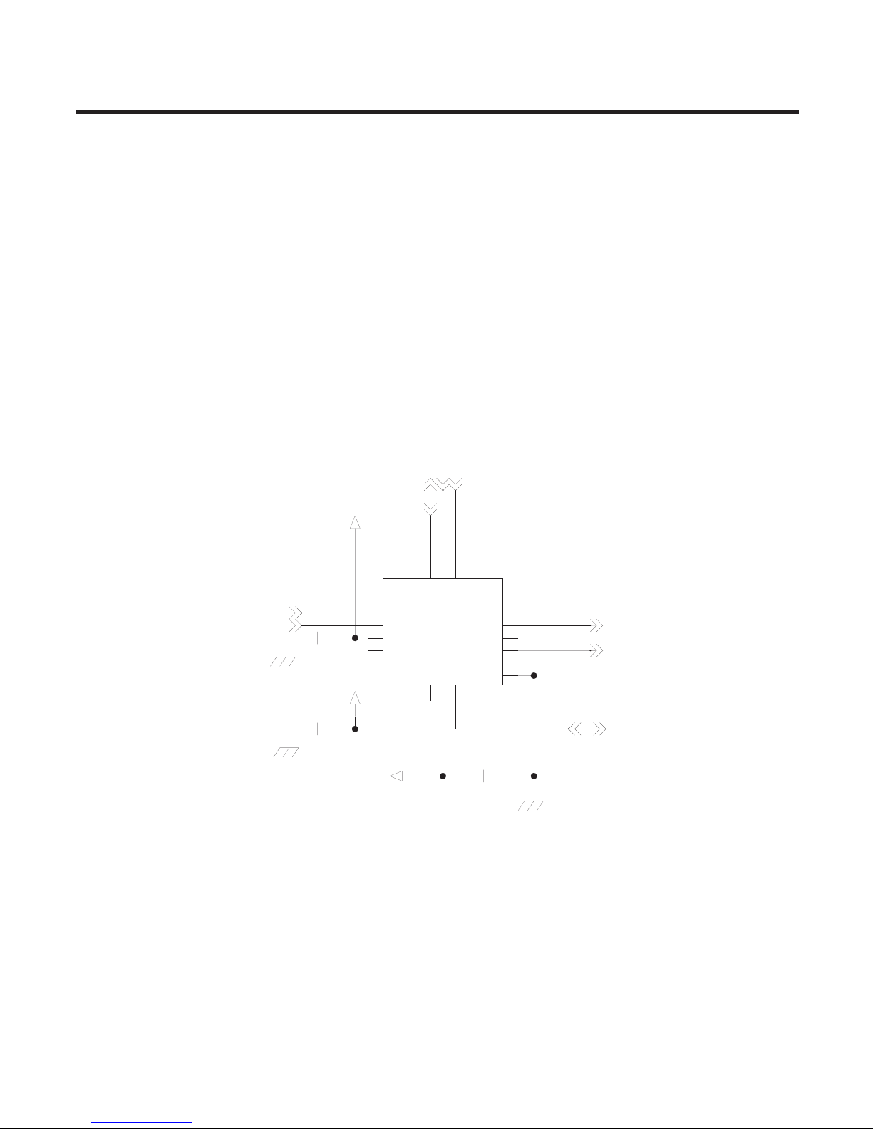
The L2000 CPU Subsystem consists of an embedded ARM1136JF-S microprocessor and peripherals, which
supports AMBA AHB bus interface(Main-AHB & Sub-AHB).
The peripherals was included the DMA Controller, DDR Controller, L2000 Modem Subsystem, EPI, P-SPI, SMI,
SRAM Controller, Flash Memory Controller, SDIO, USBs, Crypto C ell, Boot ROM, Internal SRAM by AMBA AHB
bus interface and CPU APB Bridge(AHB2APB) which controls SIM, UART0, UART1, GPIO, Timer(TMU, TMOS),
3.2.1 LTE Mod
em
(L2000, U201)
Watch D
og Timer,
I2C, Int
errupt Controller,
SYSC, CPG, DBG, by AMBA APB b
us interface.
Figure 3.8 L2000 Functional Block Diagram
3. TECHNICAL BRIEF
- 20 -
Copyright © 2011 LG Electronics. Inc. All right reserved.
Only for training and service purposes
LGE Internal Use Only
3. TECHNICAL BRIEF
3.2.2 Memory(N25Q128[VDFPN8 (F8)], U601)
The N25Q128 i
s a
128 Mbit (16Mb
x 8) serial Flash memory, w
ith ad
vanced write protection mechanisms.
It is accessed by a high speed SPI-compatible bus and features the possibility to work in XIP (“eXecution in
Place”) mode.
The N25Q128 supports innovative, high-performance quad/dual I/O instructions, these new instructions allow
to double or quadruple the transfer bandwidth for read and program operations.
Furthermore the memory can be operated with 3 different protocols:
Standard SPI (Extended SPI protocol)
Dual I/O SPI
Quad I/O SPI
The Standard SPI protocol is enriched by the new quad and dual instructions (Extended SPI protocol).
For Dual I/O SPI (DIO-SPI) all the instructions codes, the addresses and the data are always transmitted across
two data lines. For Quad I/O SPI (QIO-SPI) the instructions codes, the addresses and the data are always
transmitted across four data lines thus enabling a tremendous improvement in both random access time and
data throu
ghp
ut.
g p
The memory can work in “XIP mode”, that means the device only requires the addresses and not the
instructions to output the data. This mode dramatically reduces random access time thus enabling many
applications requiring fast code execution without shadowing the memory content on a RAM.
Figure 3.9 Memory
3. TECHNICAL BRIEF
- 21 -
Copyright © 2011 LG Electronics. Inc. All right reserved.
Only for training and service purposes
LGE Internal Use Only
3. TECHNICAL BRIEF
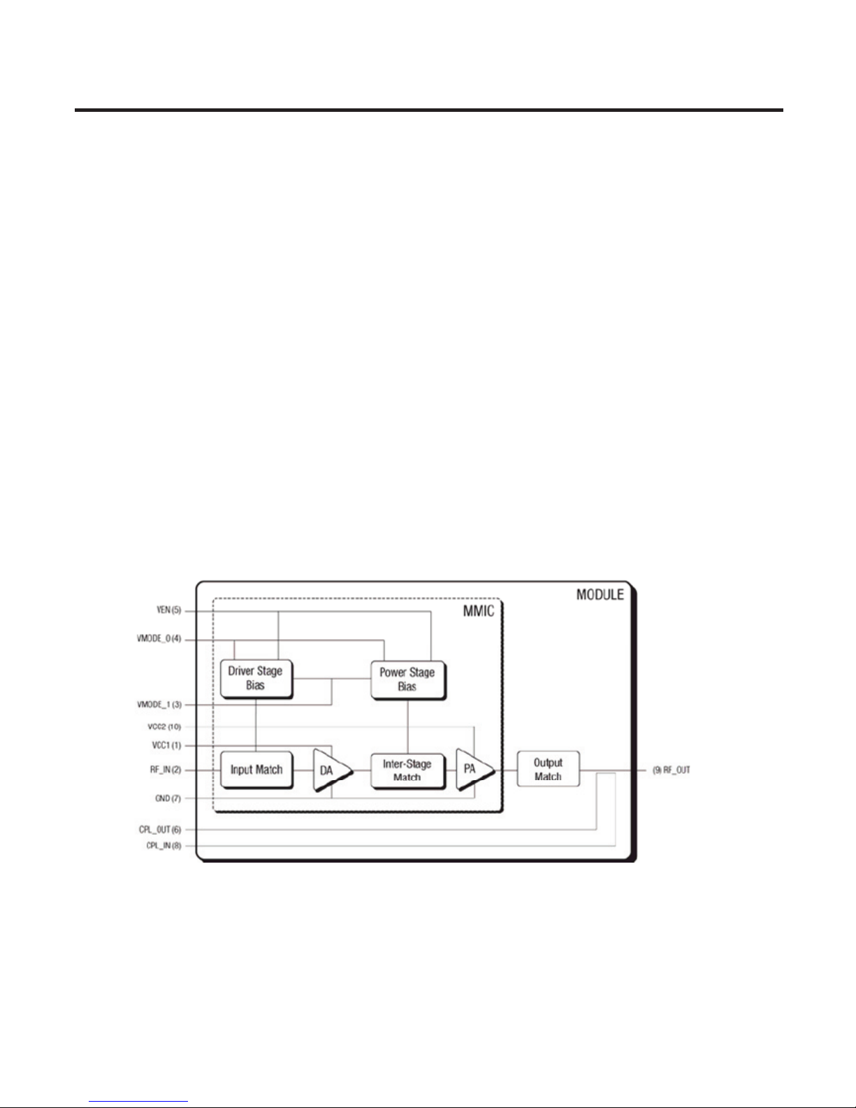
3.2.3 LTE PAM (SKY77704-8, U101, U102)
T
he SKY77704-8 Power Amplifier Module (PAM) is a fully matched, surface mount module developed for LTE /
EUTRAN applications. This small and efficient module packs full coverage of LTE Band IIX into a single
compact package.
The SKY77704-8 meets the stringent spectral linearity requirements of LTE modulation with QPSK / 16QAM
modulations from 1.4 MHz to 20 MHz bandwidth and full or partial resource block allocations with high power
added efficiency.
The single Gallium Arsenide (GaAs) Microwave Monolithic Integrated Circuit (MMIC) contains all active
circuitry in the module, including the PA, input, and interstage matching. Output match is realized offchip
within the module package to optimize efficiency and power performance into a 50 Ω load.
The SKY77704-8 is manufactured with Skyworks’ BiFET process which provides for all positive voltage DC
supply operation while maintaining high efficiency and good linearity. Primary bias is supplied via the
VCC1 and VCC2 pads directly from battery output in the 3.2 to 4.2 volt range. Power-down is accomplished by
setting a logic low level on the VEN pad. No external supply side switch is needed as typical “off” leakage is a
few microamperes with full primary voltage supplied from the battery.
The VMODE0 and VMODE1 pads are used to switch between high, medium and low power modes to reduce
current consumption and gain in the back-off conditions.
Figure 3.10 PAM Module
3. TECHNICAL BRIEF
- 22 -
Copyright © 2011 LG Electronics. Inc. All right reserved.
Only for training and service purposes
LGE Internal Use Only
3. TECHNICAL BRIEF
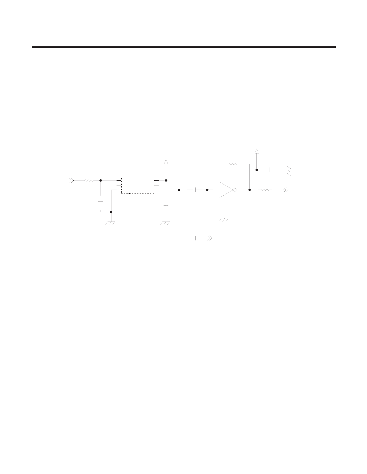
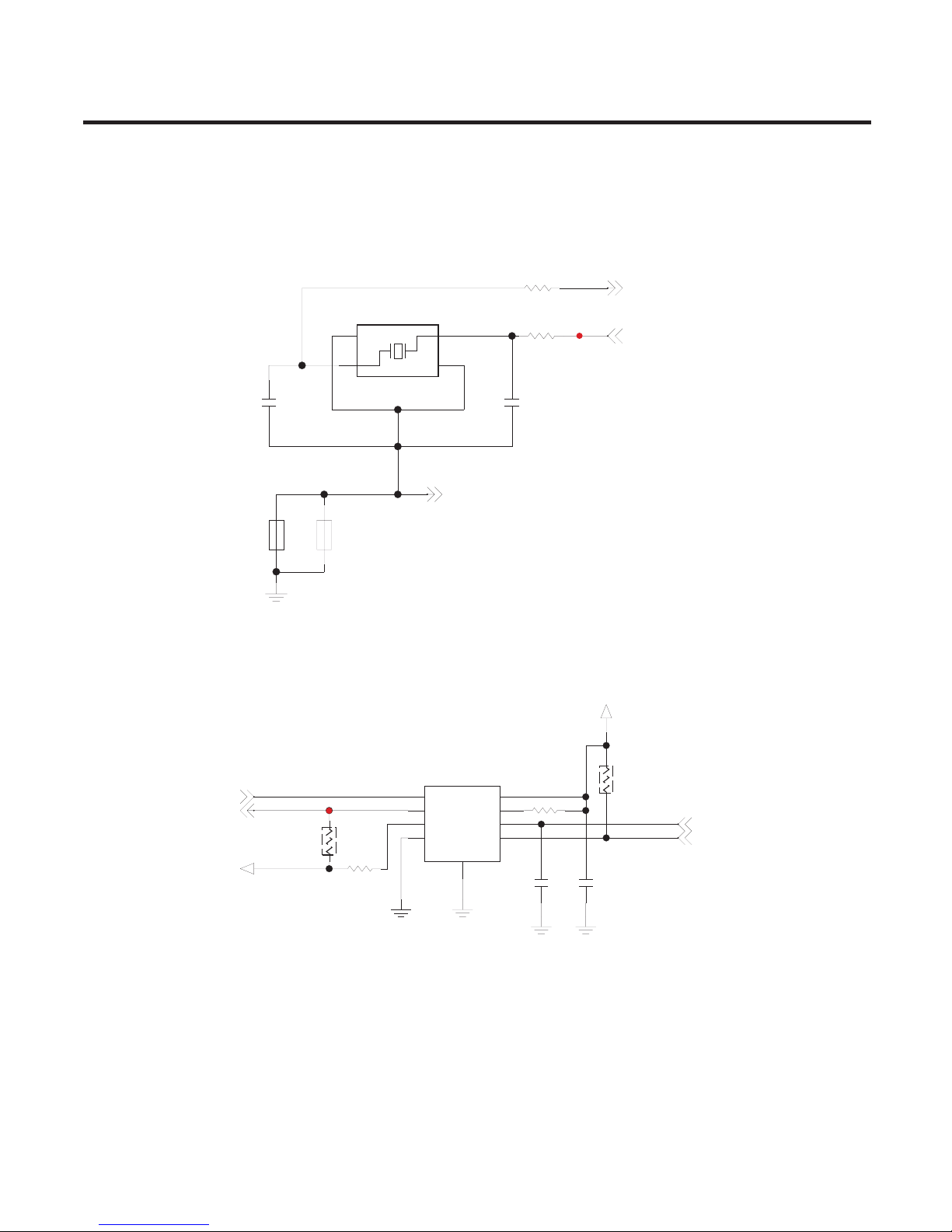
3.2.4 LTE Modem 19.2 MHz Clock (Crystal, X200)
For the generation of the reference frequency an external TCVCXO module is used.
The temperature Compensation helps to minimize the initial synchronization time within a UMTS network.
The module has no Dedicated enable pin as its supply line is routed through SMARTi UE and open if not needed.
Figure 3.11 TCXO Circuit Diagram
10n
C205
100n
C200
200KR203
2V8_TCXO
33R202
U200
NL17SZ04XV5T2G
3
42
5
VCC
GND
2V8_TCXO
10n
C201
100n
C204
33n
C203
100R200
19.2MHz
X200
TG-5025CG-19_2M
32
65
41
VC VCC
TP1 TP2
GND OUT
TCXO_IN
A
FC_OUT
REF_CLK_OUT
3. TECHNICAL BRIEF
- 23 -
Copyright © 2011 LG Electronics. Inc. All right reserved.
Only for training and service purposes
LGE Internal Use Only
3. TECHNICAL BRIEF
3.2.5 SIM interface (sub board, U600)
Xenon[FM300] supports 1.8V & 2.9V plug in SIM, SIM interface scheme is shown in figure SIM_IO, SIM_CLK,
SIM_RST ports are used to communicate with BBP(S-Gold3) and the SIM power supply enabled by PMIC.
SIM Interface
SIM_CLK : SIM card reference clock
SIM_RST : SIM card As
y
nc /sync reset
y y
SIM_IO : SIM card bidirectional reset
Figure 3.12 SIM Interface
2V6_IO
100n
C600
U600
NCN4555
2
17
5
4
1
1
31
10
11
6
3
9
8
12
4
6
151
7
C
CV_
M
IS
O
I
4CN
NC1
NC3
OI_MIS
SIM_RST
VDD
2C
N
SIM_CLK
GND
K
LC
STOP_
TS
R
TABV
G_SLUG
MOD_VCC
SYS_PWR
100n
C604
SIM_PWR
100n
C605
SIM_RST
SIM_CLK
SIM_DAT
A
SIM_PWRDOWN
SIM_PWRSEL
T
S
RM
I
S
K
L
CMIS
A
TAD
M
IS
4. TROUBLE SHOOTING
- 24 -
Copyright © 2011 LG Electronics. Inc. All right reserved.
Only for training and service purposes
LGE Internal Use Only
4. TROUBLE SHOOTING
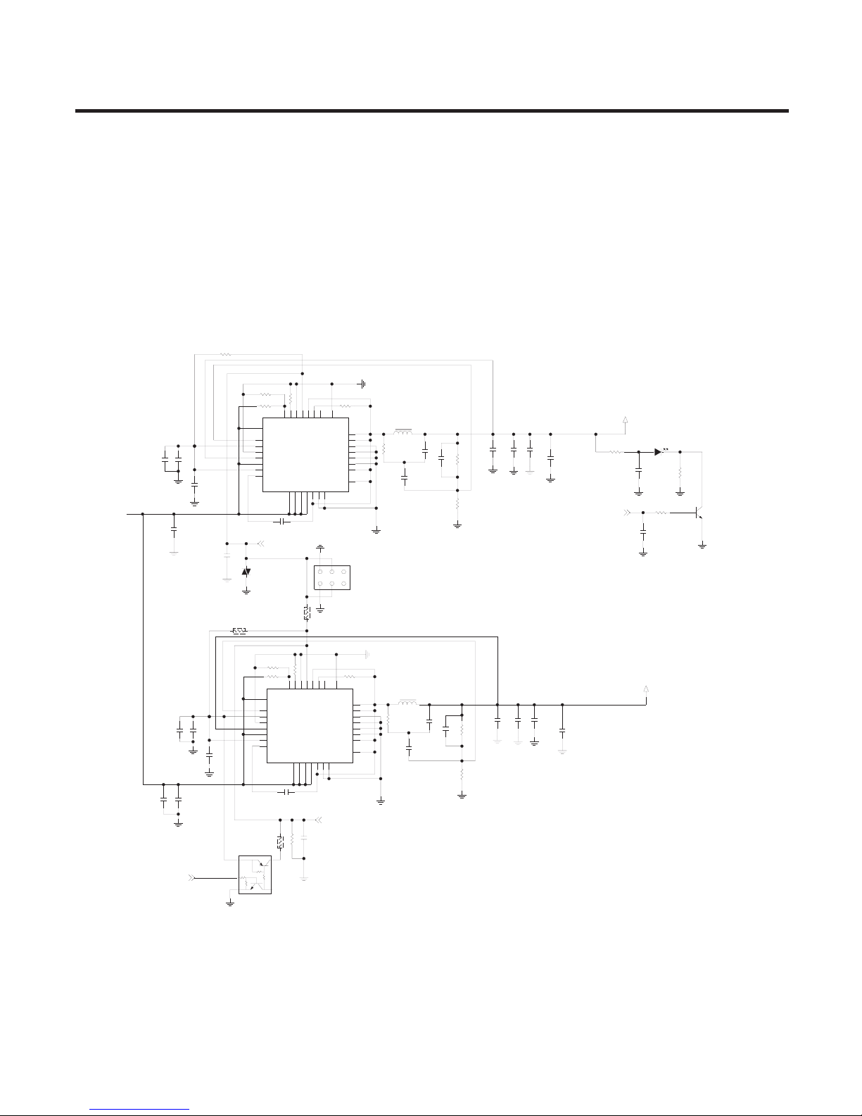
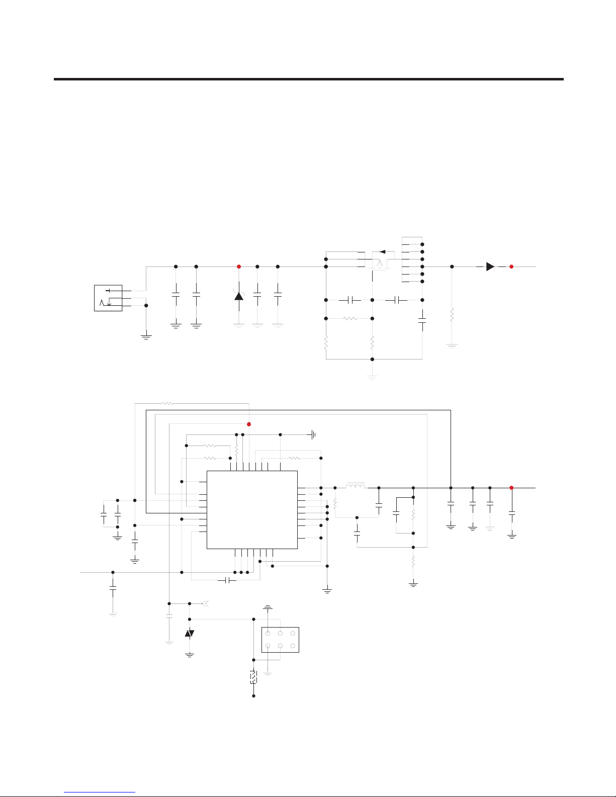
4.1 Power on Trouble – 3.3V Main power
Main source power of BCM5358U :
12V is Supplied From Adaptor to Modem Æ Passes DC/DC and 3.3V is supplied for BCM
4. TROUBLE SHOOTING
001R
IND
0.1u
C17
6
1
C
IND
02C
u
1
6
1
R
K021
0.1u
C107
71R
K
02
1
R101
DNI
CN100
ENJW0002601
KJA-DC-0-0037
4
5
3
10n
C108
ZD100
EAH61438301
PSD24C-LF
1
2
Q1
EBK61571901
SI7121DN
1S
2S
3S
G
1D 2D 3D 4D 5D 6D 7D
C106
DNI DNI
C109
D1
EDSY0020101
B340A
C3
1u
C8
2.2u
C9
10n
2R
K1.
9
1
C12
47p
C1
DNI
SPPH410100
435
261
2
0
1NC
ESPY0001701
C4 1u
0
1R
K
7
4
U2
EUSY0369702
SC424
3
31
6
1
30
32
72
92
62
22
01
52
15
31
16
20
19
82
41
21
8
9
7
2
42
2
1
5
18
11
174
VOUT PGND4
4NIV
PGND5
VIN
TSBXL
SXL
V5V
BST
2NIV
1N
IV
LX3
2DNGP
LNE
PGND6
LX2
PGND3
1DNGP
LX1
VSP/NE
3NIV
DO
OGP
2D
N
GA
3DNGA
NO
T
MILI
VIN5
FB
VLDO
LX4
AGND1
R11 100K
C18
100n
C115
DNI
L100
2.2u
R14 100K
VA100
C15
10u
0.1u
C103
R8 2.7K
C104
22u
551R I
N
D
6R
K61
3R
K65
R102 100K
C101
22u
C102
22u
NP_EN
TP1 TP2
TP3
TP4
4. TROUBLE SHOOTING
- 25 -
Copyright © 2011 LG Electronics. Inc. All right reserved.
Only for training and service purposes
LGE Internal Use Only
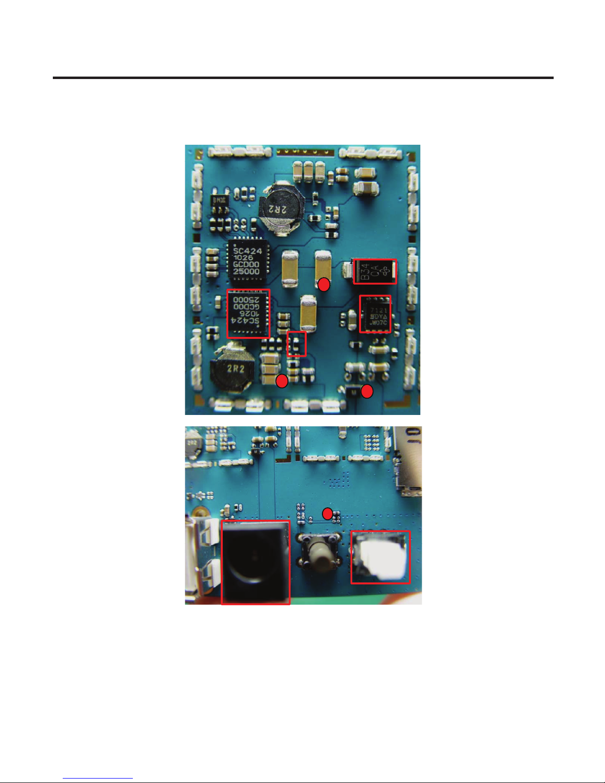
4. TROUBLE SHOOTING
D1
TP2 Q1
U2
R14
TP4
TP1
TP3
CN100
CN102
4. TROUBLE SHOOTING
- 26 -
Copyright © 2011 LG Electronics. Inc. All right reserved.
Only for training and service purposes
LGE Internal Use Only
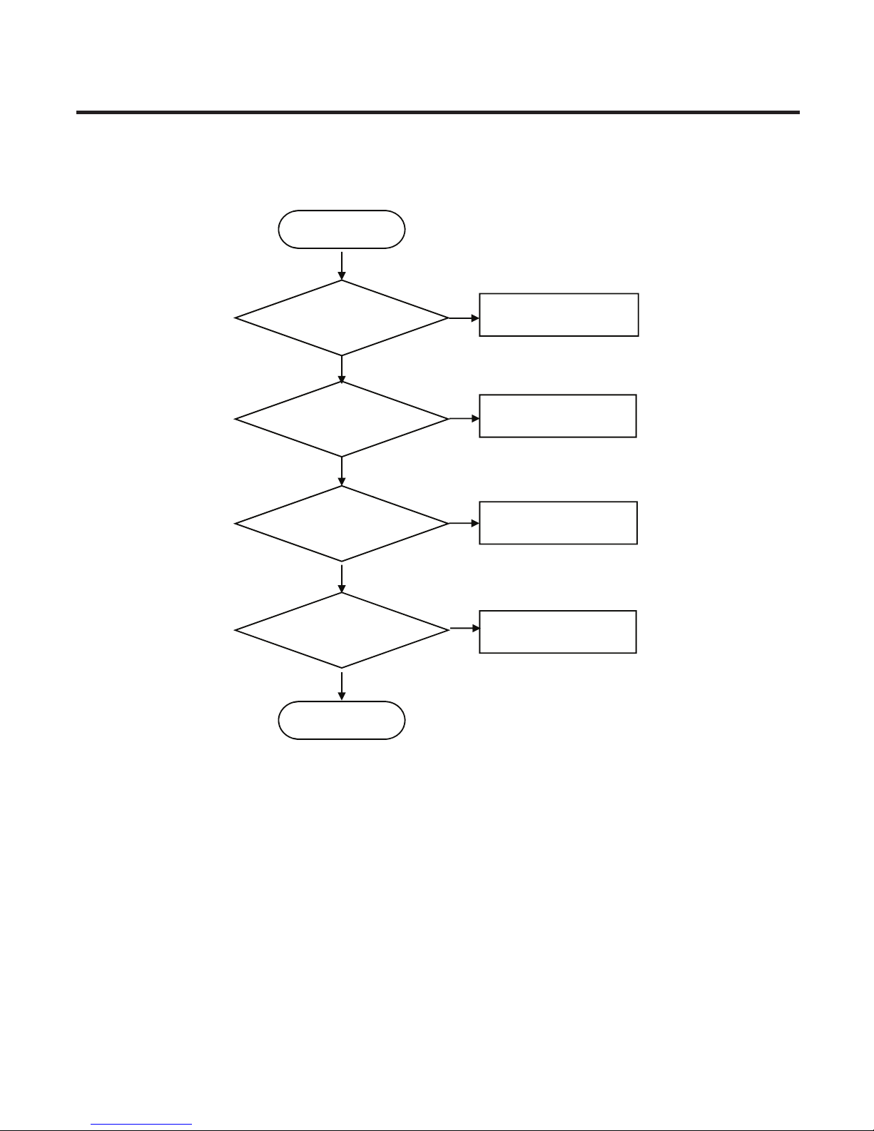
(1) Check the 12V
voltage(TP1)
No
Check soldering CN100(
DC-Jack) or replace
START
(2) Check the 12V
voltage(TP2)
Yes
No
Check soldering
Q1 & D1
Yes
(3) Push the PWR S/W
Check TP3 is high?
No
Check soldering CN102&
R14.
(4) Check the TP4
Check soldering of U2 or
No
Yes
Yes
T
P4= 3.3V
replace
FINISH
4. TROUBLE SHOOTING
- 27 -
Copyright © 2011 LG Electronics. Inc. All right reserved.
Only for training and service purposes
LGE Internal Use Only
4. TROUBLE SHOOTING
4.2 Power on Trouble – BCM Booting Trouble
Q103
EBK61591901
SIA426DJ
D1 D2 D3 D4 D5
G
S1 S2
0R144
1u
C111
R152 0
0R154
1
R140
VDD_3.3
4
01Q
EQBP0008701
2SB1424
1
3
2
C
E
B
Q102
EBK61473001
SI7403BDN
S1 S2 S3
G
D1 D2 D3 D4 D5 D6 D7
1
R141
VDD_3.3
10u
C133
0.1u
C134
IND93
1
R
VDD_1.2
VDD_2.5
0.1u
C139
0.1u
C149
10u
C150
C156
22u
L102
EAP61746101
NR5040T3R3N
3.3u
22u
C135
22u
C136
VCNTL
SWREG_NDRIVE
SWREG_PDRIVE
VSENSE2P5
SWREG_VFB_SEN
TP1
TP2
TP3
TP4
TP5
4. TROUBLE SHOOTING
- 28 -
Copyright © 2011 LG Electronics. Inc. All right reserved.
Only for training and service purposes
LGE Internal Use Only
0.1u
C224
I
N
D
332R
10K
R238
10KR231
DNI
C223
VDD_3.3
VDD_3.3
DNI
R224
U202
EUSY0432601
N25Q128-A13BF840E
9
54
63
72
81
S_ VCC
DQ1 HOLD_/DQ3
W_VPP/DQ2 C
VSS DQ0
G_SLUG
SFLASH_DATA_IN
SFLASH_CS
SFLASH_DATA_OUT
SFLASH_CLK
SERIAL FLASH[128Mb]
600
FB400
220
R407
0R406
33p
C422
33p
C423
20MHz
CXC3X200000GHVRG00
EXXY0027801
X400
4
2
3
1
HOT1
HOT2
GND1
GND2
600
FB401
XTAL_OUT
XTAL_IN
XTAL_GND
GND
20MHz CRYSTAL
TP7
TP6
4. TROUBLE SHOOTING
- 29 -
Copyright © 2011 LG Electronics. Inc. All right reserved.
Only for training and service purposes
LGE Internal Use Only
4. TROUBLE SHOOTING
TP6
X400
TP2
TP3
R140
R141
Q103
U202
TP1
Q102
L102
TP7
TP5
Q104
TP4
R152
4. TROUBLE SHOOTING
- 30 -
Copyright © 2011 LG Electronics. Inc. All right reserved.
Only for training and service purposes
LGE Internal Use Only
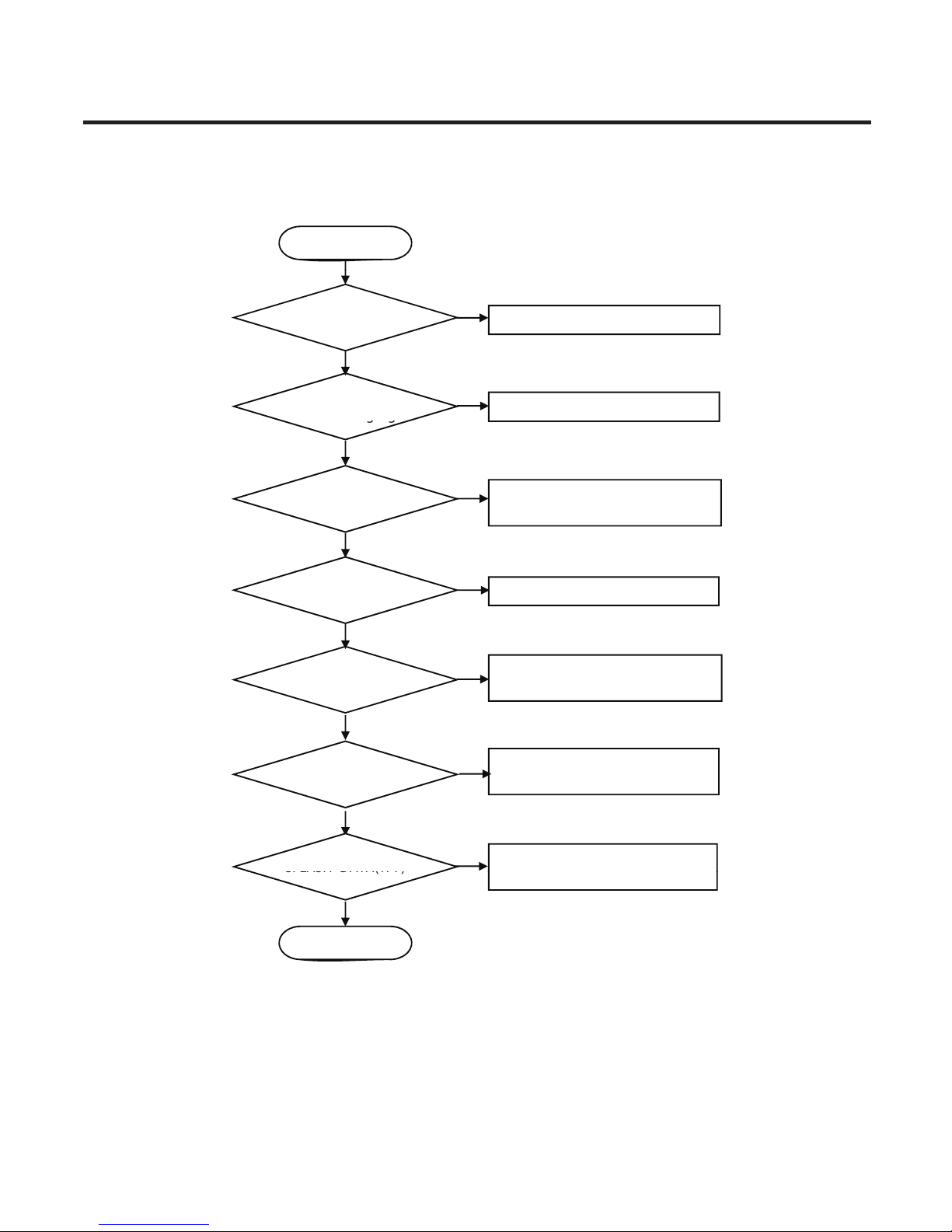
START
(1) Check TP1
TP1= Switching Signal
(2) Check TP2
T
P2 = Switching Signal
Yes
No
Check the R140 Soldering
No
Check the R141 Soldering
g g
(3) Check core
voltage(TP3)
TP3= 1.2V
Yes
No
Check Soldering Q102, Q103 L102
If soldering is fine, replace them
Yes
(5) Check voltage(TP5)
TP5= 2.5V
Yes
No
Check the Q104 Soldering
If soldering is fine, replace Q104
(4) Check voltage(TP4)
TP4= 2.5V
Check the R152 Soldering
N
o
Yes
(6) Check XTAL_OUT
Signal (TP6)
TP6= 20MHz
No
Check the X400 Soldering
If soldering is fine, replace X400
Yes
(7) Check
No
Check the U202 Soldering
FINISH
SFLASH_DATA(TP7)
TP7= Data pulse
If
soldering is fine, replace
U202
Yes
 Loading...