

LG FFH-818 Schematic
4
SERVICING PRECAUTIONS
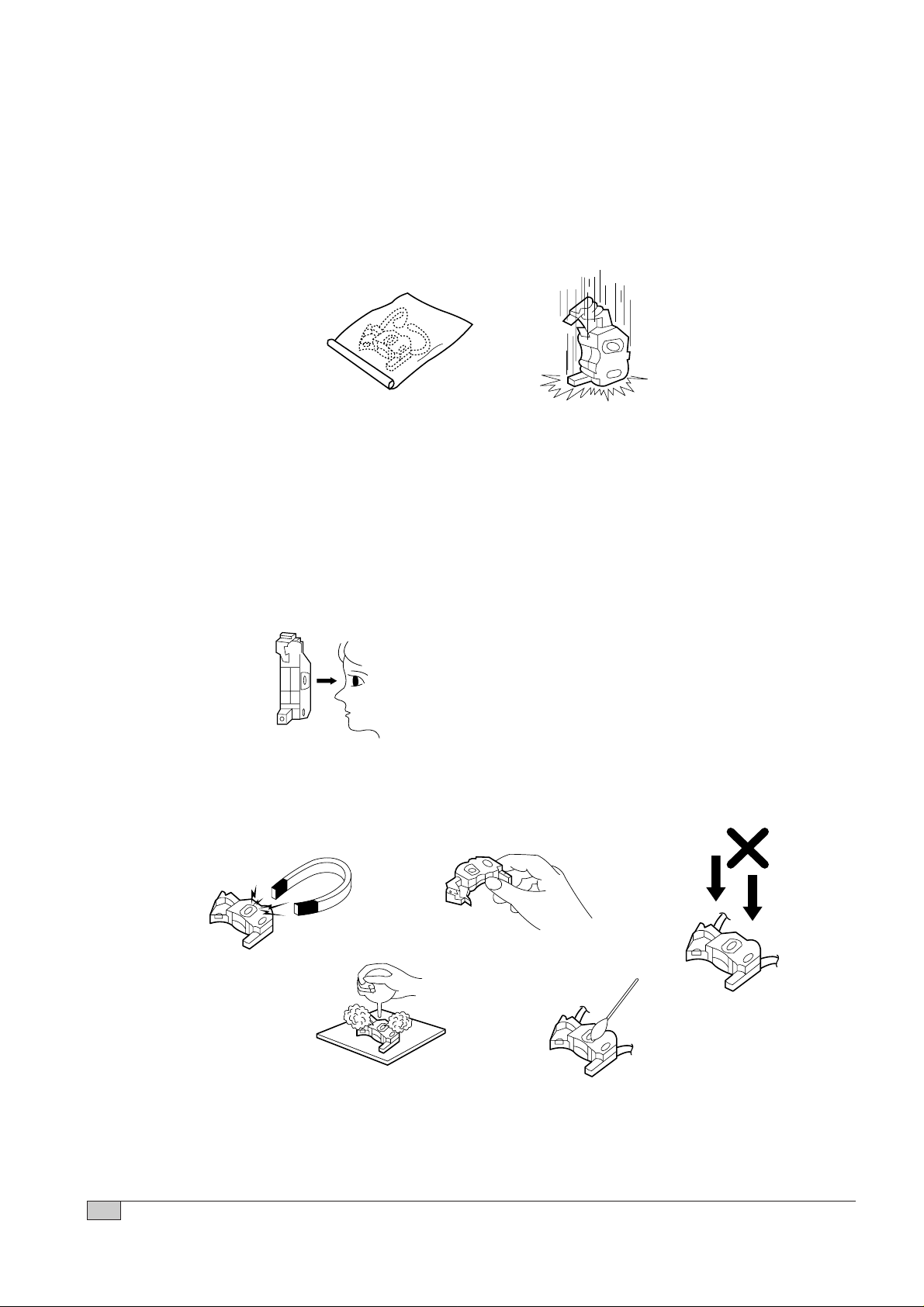
NOTES REGARDING HANDLING OF THE PICK-UP
1. Notes for transport and storage
1) The pick-up should always be left in its conductive bag until immediately prior to use.
2) The pick-up should never be subjected to external pressure or impact.
2. Repair notes
1) The pick-up incorporates a strong magnet, and so should never be brought close to magnetic materials.
2) The pick-up should always be handled correctly and carefully, taking care to avoid external pressure and
impact. If it is subjected to strong pressure or impact, the result may be an operational malfunction and/or
damage to the printed-circuit board.
3) Each and every pick-up is already individually adjusted to a high degree of precision, and for that reason
the adjustment point and installation screws should absolutely never be touched.
4) Laser beams may damage the eyes!
Absolutely never permit laser beams to enter the eyes!
Also NEVER switch ON the power to the laser output part (lens, etc.) of the pick-up if it is damaged.
5) Cleaning the lens surface
If there is dust on the lens surface, the dust should be cleaned away by using an air bush (such as used
for camera lens). The lens is held by a delicate spring. When cleaning the lens surface, therefore, a
cotton swab should be used, taking care not to distort this.
6) Never attempt to disassemble the pick-up.
Spring by excess pressure. If the lens is extremely dirty, apply isopropyl alcohol to the cotton swab. (Do
not use any other liquid cleaners, because they will damage the lens.) Take care not to use too much of
this alcohol on the swab, and do not allow the alcohol to get inside the pick-up.
Storage in conductive bag
Drop impact
NEVER look directly at the laser beam, and don
¡˙t let
contact fingers or other exposed skin.
Magnet
How to hold the pick-up
Pressure
Pressure
Cotton swab
Conductive Sheet
5
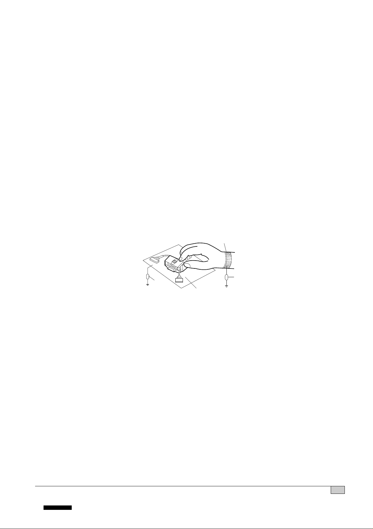
NOTES REGARDING COMPACT DISC PLAYER REPAIRS
1. Preparations
1) Compact disc players incorporate a great many ICs as well as the pick-up (laser diode). These
components are sensitive to, and easily affected by, static electricity. If such static electricity is high
voltage, components can be damaged, and for that reason components should be handled with care.
2) The pick-up is composed of many optical components and other high-precision components. Care must
be taken, therefore, to avoid repair or storage where the temperature of humidity is high, where strong
magnetism is present, or where there is excessive dust.
2. Notes for repair
1) Before replacing a component part, first disconnect the power supply lead wire from the unit
2) All equipment, measuring instruments and tools must be grounded.
3) The workbench should be covered with a conductive sheet and grounded.
When removing the laser pick-up from its conductive bag, do not place the pick-up on the bag. (This is
because there is the possibility of damage by static electricity.)
4) To prevent AC leakage, the metal part of the soldering iron should be grounded.
5) Workers should be grounded by an armband (1MΩ)
6) Care should be taken not to permit the laser pick-up to come in contact with clothing, in order to prevent
static electricity changes in the clothing to escape from the armband.
7) The laser beam from the pick-up should NEVER be directly facing the eyes or bare skin.
Armband
Conductive
Sheet
Resistor
(1 Mohm)
Resistor
(1 Mohm)

6
ESD PRECAUTIONS
Electrostatically Sensitive Devices (ESD)
Some semiconductor (solid state) devices can be damaged easily by static electricity. Such components
commonly are called Electrostatically Sensitive Devices (ESD). Examples of typical ESD devices are integrated
circuits and some field-effect transistors and semiconductor chip components. The following techniques should
be used to help reduce the incidence of component damage caused by static electricity.
1. Immediately before handling any semiconductor component or semiconductor-equipped assembly, drain off
any electrostatic charge on your body by touching a known earth ground. Alternatively, obtain and wear a
commercially available discharging wrist strap device, which should be removed for potential shock reasons
prior to applying power to the unit under test.
2. After removing an electrical assembly equipped with ESD devices, place the assembly on a conductive
surface such as aluminum foil, to prevent electrostatic charge buildup or exposure of the assembly.
3. Use only a grounded-tip soldering iron to solder or unsolder ESD devices.
4. Use only an anti-static solder removal device. Some solder removal devices not classified as "anti-static" can
generate electrical charges sufficient to damage ESD devices.
5. Do not use freon-propelled chemicals. These can generate electrical charges sufficient to damage ESD
devices.
6. Do not remove a replacement ESD device from its protective package until immediately before you are
ready to install it. (Most replacement ESD devices are packaged with leads electrically shorted together by
conductive foam, aluminum foil or comparable conductive materials).
7. Immediately before removing the protective material from the leads of a replacement ESD device, touch the
protective material to the chassis or circuit assembly into which the device will by installed.
CAUTION : BE SURE NO POWER IS APPLIED TO THE CHASSIS OR CIRCUIT, AND OBSERVE ALL OTHER
SAFETY PRECAUTIONS.
8. Minimize bodily motions when handing unpackaged replacement ESD devices. (Otherwise harmless motion
such as the brushing together of your clothes fabric or the lifting of your foot from a carpeted floor can
generate static electricity sufficient to damage an ESD device).
- 30 -
Pre Out
Ch2
3.3µF
3.3µF
3.3µF
3.3µF
3.3µF
1000µF
1000µF
47µF
47µF
47µF
0.018µF
1000µF
3.3µF
47µF
1.2µF
100
µF
R . R
Vcc
1000
µF
47µF
0.018µF
10kΩ
10kΩ
150kΩ
150kΩ
1MΩ
2.2kΩ
2.2kΩ
Rec IN
Ch2
Rec
IN
Rec IN
Ch1
ALC
Rec Out
Ch2
180kΩ
180kΩ
Gv
Gvo
180kΩ
180kΩ
1kΩ
1kΩ
1kΩ
1kΩ
100kΩ
100Ω
10kΩ
10kΩ
10Ω
300kΩ
9.1kΩ
100Ω
Pre IN
Ch2/B
(Play Rec)
Pre IN
Ch2/A
(Play only)
Pre IN
Ch1/B
(Play Rec)
Pre Out
Ch1
Pre IN
Ch1/A
Ch1/B
NF
Ch2/A
Ch1/A
Ch1/B
Gvo
Gv
Gvo
Gv
Vcc
M
N
NF
NF
Ch1
Ch1
Ch2
Gvc
GV
Ch2
ALC
GND
Rec
15
14
13
12
11
23
24
1
2
161718192122
IN
Vref1
Vref
Vref2
A/B
Metal
Out
Pre
Out
REC
Out
Rec Out
Ch1
Mix
Out
GND1 M/N
6.8kΩ
A
B
1000pF
1000pF
6.8kΩ
9.1kΩ
20
10 9876435
M/N
REC SW REC SWGND P/B SW P/B SWCONT GND GNDV
CC
123456789
KA3082
KIA6289N
- 30 -
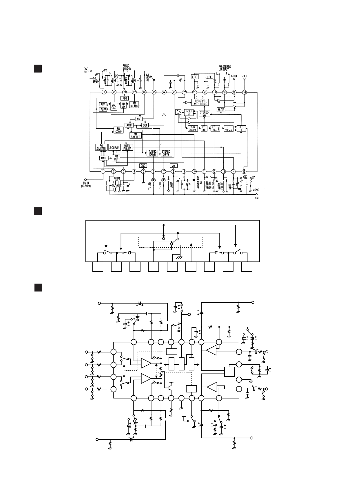
INTERNAL BLOCK DIAGRAM OF ICs
LA1837
- 31 -
KA8301
KIA7805 P/PI ~ KIA7824P/PI
DRIVER
PRE
LOGIC
2 3 4 5 6 7 8 9 101
GND
Vout1
Vz1VrFin
Rin
Vcc1
Vcc2
Vz2
Vout2
3
1
2
4
R
12
R
1
C
21
R
12
Q
1
Q
7
Q
13
Q
10
Q
6
Q
5
Q
4
Q
3
Q
11
Q
15
Q
14
Q
9
Q
8
Q
16
Q
17
Q
INPUT
OUTPUT
GND
2
Q
1
Z
18
R
8
R
9
R
13
R
11
R
17
R
5
R
6
R
1
R
2
R R
16
R
20
R
19
R
14
R
10
R
7
R
- 32 -
LC7273M
TDA7440D
+5V
+5V
VREF
CINFLOUTVREF
Vdda
Vssa
MPXIN
TEST
XIN XOUT
Vssd
Vddd
RDCL
RDDA
MODE
RST
RDS-ID
READY
CLK(4.332MHz)
SMOOTHING
FILTER
OSC
PLL
(57kHz)
DATA
DECODER
RAM
(128bit)
RDS-ID
DETECT
CLOCK
RECOVERY
(1187.5Hz)
ANTIALIASING
FILTER
REFERENCE
VOLTAGE
57kHz
BPF
(SCF)
TEST
L-IN1
100K
100K
100K
100K
100K
100K
100K
100K
4 8 9 18
27
21
22
20
26
24
25
LOUT
SCL
SDA
DIG_GND
ROUT
V
S
AGND
R
B
R
B
14 15
10 11 19 12 13 23
5
G
G
6
7
3
2
INPUT MULTIPLEXER
+GAIN
MUXOUTR INR TREBLE(R) BIN(R) BOUT(R) CREF D98AU883
0/30dB
2dB STEP
MUXOUTL
VOLUME TREBLE
I CBUS DECODER + LATCHES
BASS
SPKR ATT
LEFT
VOLUME TREBLE BASS
SUPPLY
V
REF
SPKR ATT
RIGHT
INL TREBLE(L) BOUT(L)BIN(L)
1
28
L-IN2
L-IN3
L-IN4
R-IN1
R-IN2
R-IN3
R-IN4
2
- 33 -
STK411-220E
- 34 -
MSGEQ7
Audio
In
Anti-Alias
Filter
Clock
Oscillator
Output
Multiplexor
CKIN
Reset
63Hz
Bandpass
160Hz
Bandpass
400Hz
Bandpass
1kHz
Bandpass
2.5kHz
Bandpass
6.25kHz
Bandpass
16kHz
Bandpass
Peak
Detector
Peak
Detector
Peak
Detector
Peak
Detector
Peak
Detector
Peak
Detector
Peak
Detector
Strobe
DC Out
LC72131, 72131M
B01 B02 B03 B04 I01 I02
XIN
PD
AIN
AOUT
IFIN
XOUT
FMIN
AMIN
CE
DI
CL
D0
VDD
VSS
REFERENCE
DIVIDER
PHASE DETECTOR
CHARGE PUMP
UNLOCK
DETECTOR
UNIVERSAL
COUNTER
DATA SHIFT REGISTER
LATCH
12bits PROGRAMMABLE
DIVIDER
SWALLOW COUNTER
1/16. 1/17 4bits
POWER
ON
RESET
CCB
I/F
1
2
- 35 -
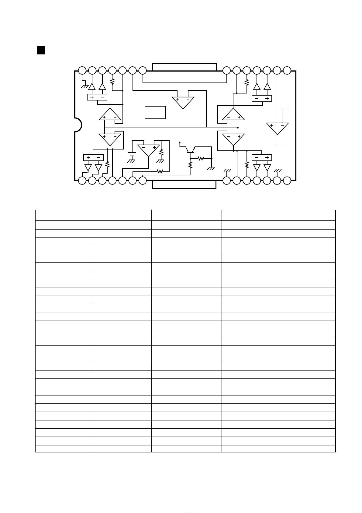
KA3010
PIN DESCRIPTION
28 27
26 25 24 23 22
T S D
REGULATOR
MUTE
LEVEL
SHIFT
LEVEL
SHIFT
100K
50K
50K
10K
10K
10K 10K
10K
BUY
BUY
BUY
LEVEL
SHIFT
LEVEL
SHIFT
1 2 3 4 5 6 7
8 9 10 11 12 13 14
21 20 19 18 17 16 15
Pin No. Symbol I/O Description
1 DO1.1 O DRIVE OUTPUT
2 DO1.2 O DRIVE OUTPUT
3 DI1.1 I DRIVE INPUT
4 DI1.2 I DRIVE INPUT
5 REG REGULATOR
6 REO O REGULATOR OUTPUT
7 MUTE MUTE
8 GND1 GROUND
9 DI2.1 I DRIVE INPUT
10 DI2.2 I DRIVE INPUT
11 DO2.1 O DRIVE OUTPUT
12 DO2.2 O DRIVE OUTPUT
13 GND2 GROUND
14 OPOUT O OPAMP OUTPUT
15 OPIN (-) I OPAMP OUTPUT (-)
16 OPIN (+) I OPAMP INPUT (+)
17 DO3.1 O DRIVE OUTPUT
18 DO3.2 O DRIVE OUTPUT
19 DI3.1 I DRIVE INPUT
20 DI3.2 I DRIVE INPUT
21 VCC1 SUPPLY VOLTAGE
22 VCC2 SUPPLY VOLTAGE
23 VREF 2.5V BIAS VOLTAGE
24 DI4.1 I DRIVE INPUT
25 DI4.2 I DRIVE INPUT
26 DO4.1 O DRIVE OUTPUT
27 DO4.2 O DRIVE OUTPUT
28 GND3 GROUND
- 36 -
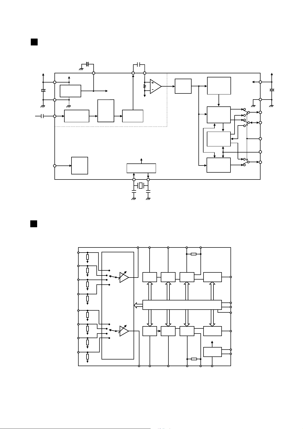
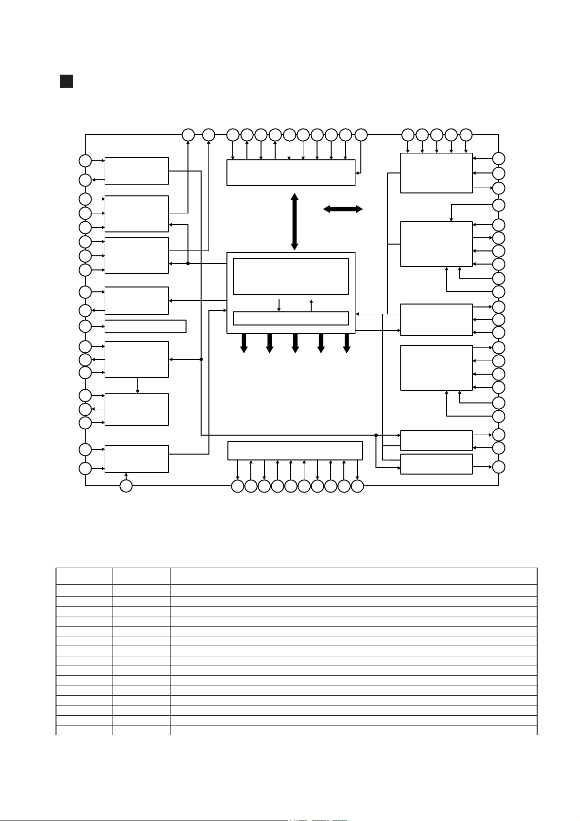
KB9223
MICOM TO SERVO CONTROL
AUTO SEQUENCER
FOK DETECTION
CIRCUIT
MIRROR DETECTION
CIRCUIT
Spindle Servo LPF
(Double Speed)
Sled Servo Amplifier
& Sled Kick GEN.
Tracking Phase
Compensation Block
& Jump Pulse GEN.
Focus Phase
Compensation
& Offset cancel circuit
Micom Data
Interface Logic
RF Amp
73
74
65
66
63
67
68
79
69
70
71
78
76
75
32
33
77
2
4
RF-
RFO
PD1
PD2
F
E
EI
PD
LD
VR
ARF
IRF
ASY
EFM
RFI
DCB
DCC1
GC1O
MLT
TZC
FE2
FLB
FGD
FS3
TE1
FE1
GC1I
CH1O
CH1I
MUTEI
RRC
CH2O
CH2I
GC2I
GC2O
5
15 16 13 14 19 17 12 11 9 10
40
1
39
6
25
24
23
45
46
42
44
43
61
62
55
53
50
49
57
48
47
60
FOK
MCP
MIRROR
FSET
SMEF
SMON
FS1 to
FS4
TM1 to
TM6
BAL1 to
BAL5
PS1 to
PS4
GA1 to
GA5
SMPD
SPDL-
SPDLO
SL+
SL-
SLO
TGU
TG2
LPFT
TE2
TEO
TE-
TDFCT
FEO
FE-
FDFCT
327282658525135363738312930225459
APC Amp
Center Voltage Amp.
Focus Error Amp
FE-BIAS Adjustment
Tracking Error Amp
E/F Balance & Gain
Control
RF Level AGC
&
Equalizer
EFM
Comparator
Defect Detection
CircuitT
ADJUSTMENT-FREE CONTROL
Built-in Post Filter Amp(L&R)
LDON
PIN DESCRIPTION
Pin No. System Description
1 MCP Capacitor connection pin for mirror hold
2 DCB Capacitor connection pin for defect Bottom hold
3 FRSH. Capacitor connection pin for time constant to generate focus search waveform
4 DCC2 The input pin through capacitor of defect bottom hold output
5 DCC1 The output pin of defect bottom hold
6 FSET The peak frequency setting pin for focus, tracking servo and cut off frequency of CLV LPF
7 VDDA Analog VCC for servo part
8 VCCP VCC for post filter
9 GC2I Amplifier negative input pin for gain and low pass filtering of DAC output CH2
10 GC2O Amplifier output pin for gain and low pass filtering of DAC output CH2
11 CH2I The input pin for post filter channel2
12 CH2O The output pin for post filter channel2
13 CH1O The output pin for post filter channl1
14 CH1I The input pin for post filter channel1
15 GC1O Amplifier output pin for gain and low pass filtering of DAC output CH1
 Loading...