

Page 1

- 1-1 -
CONTENTS
SECTION 1. GENERAL
• SERVICING PRECAUTIONS
....................................................................................................................
1-2
• ESD PRECAUTIONS
.................................................................................................................................
1-4
• SPECIFICATIONS
.....................................................................................................................................
1-5
SECTION 2. ELECTRICAL
• ADJUSTMENTS
.........................................................................................................................................
2-1
• TROUBLESHOOTING
...............................................................................................................................
2-3
• WAVEFORMS OF MAJOR CHECK POINT
..............................................................................................
2-7
• BLOCK DIAGRAM
...................................................................................................................................
2-17
• SCHEMATIC DIAGRAMS
........................................................................................................................
2-19
• WIRING DIAGRAM
..................................................................................................................................
2-29
• PRINTED CIRCUIT DIARGAMS
..............................................................................................................
2-31
• INTERNAL BLOCK DIAGRAM OF IC’s
...................................................................................................
2-38
• REPAIRS REGARDING CD MECHANISM
.............................................................................................
2-45
SECTION 3. EXPLODED VIEWS
• CABINET AND MAIN FRAME SECTION
.................................................................................................
3-1
• TAPE DECK MECHANISM: AUTO STOP DECK(OPTIONAL)
..................................................................
3-3
• TAPE DECK MECHANISM: AUTO REVERSE DECK
................................................................................
3-5
• CD MECHANISM
........................................................................................................................................
3-7
SECTION 4. SPEAKER
..................................................................................................................
4-1
SECTION 5. REPLACEMENT PARTS LIST
..................................................................................
5-1
Page 2
SECTION 1. GENERAL
SERVICING PRECAUTIONS
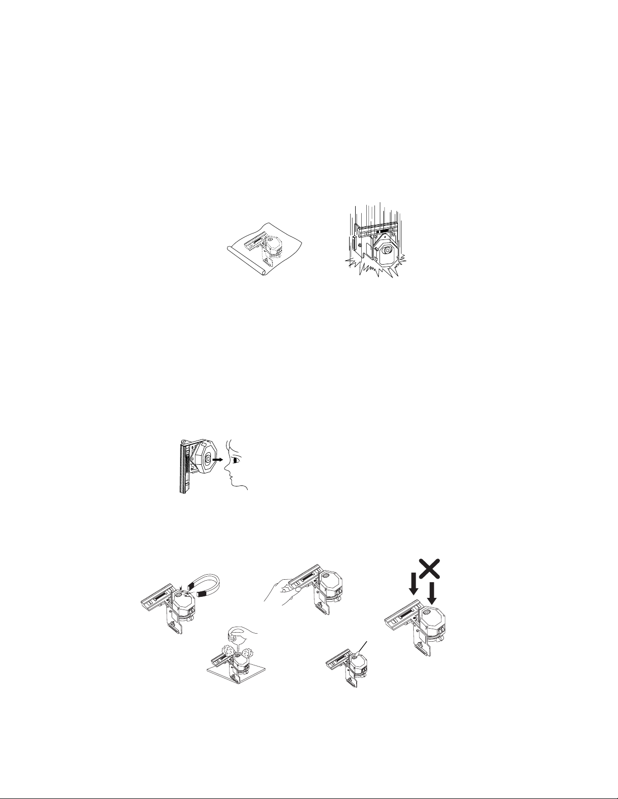
NOTES REGARDING HANDLING OF THE PICK-UP
1. Notes for transport and storage
1) The pick-up should always be left in its conductive bag until immediately prior to use.
2) The pick-up should never be subjected to external pressure or impact.
2. Repair notes
1) The pick-up incorporates a strong magnet, and so should never be brought close to magnetic materials.
2) The pick-up should always be handled correctly and carefully, taking care to avoid external pressure and
impact. If it is subjected to strong pressure or impact, the result may be an operational malfunction and/or
damage to the printed-circuit board.
3) Each and every pick-up is already individually adjusted to a high degree of precision, and for that reason
the adjustment point and installation screws should absolutely never be touched.
4) Laser beams may damage the eyes!
Absolutely never permit laser beams to enter the eyes!
Also NEVER switch ON the power to the laser output part (lens, etc.) of the pick-up if it is damaged.
5) Cleaning the lens surface
If there is dust on the lens surface, the dust should be cleaned away by using an air bush (such as used
for camera lens). The lens is held by a delicate spring. When cleaning the lens surface, therefore, a
cotton swab should be used, taking care not to distort this.
6) Never attempt to disassemble the pick-up.
Spring by excess pressure. If the lens is extremely dirty, apply isopropyl alcohol to the cotton swab. (Do
not use any other liquid cleaners, because they will damage the lens.) Take care not to use too much of
this alcohol on the swab, and do not allow the alcohol to get inside the pick-up.
- 1-2 -
Storage in conductive bag
Drop impact
NEVER look directly at the laser beam, and don’t let
contact fingers or other exposed skin.
Magnet
How to hold the pick-up
Pressure
Pressure
Cotton swab
Conductive Sheet
Page 3
NOTES REGARDING COMPACT DISC PLAYER REPAIRS
1. Preparations
1) Compact disc players incorporate a great many ICs as well as the pick-up (laser diode). These
components are sensitive to, and easily affected by, static electricity. If such static electricity is high
voltage, components can be damaged, and for that reason components should be handled with care.
2) The pick-up is composed of many optical components and other high-precision components. Care must
be taken, therefore, to avoid repair or storage where the temperature of humidity is high, where strong
magnetism is present, or where there is excessive dust.
2. Notes for repair
1) Before replacing a component part, first disconnect the power supply lead wire from the unit
2) All equipment, measuring instruments and tools must be grounded.
3) The workbench should be covered with a conductive sheet and grounded.
When removing the laser pick-up from its conductive bag, do not place the pick-up on the bag. (This is
because there is the possibility of damage by static electricity.)
4) To prevent AC leakage, the metal part of the soldering iron should be grounded.
5) Workers should be grounded by an armband (1MΩ)
6) Care should be taken not to permit the laser pick-up to come in contact with clothing, in order to prevent
static electricity changes in the clothing to escape from the armband.
7) The laser beam from the pick-up should NEVER be directly facing the eyes or bare skin.
CLEARING MALFUNCTION
You can reset your unit to initial status if malfunction occur(button malfunction, display, etc.).
Using a pointed good conductor(such as driver), simply short the RESET jump wire on the inside of the
volume knob for more than 3 seconds.
If you reset your unit, you must reenter all its settings(stations, clock, timer)
NOTE: 1. To operate the RESET jump wire, pull the volume rotary knob and release it.
2. If you wish to operate the RESET jump wire, it is necessary to unplug the power cord.
- 1-3 -
Armband
Conductive
Sheet
Resistor
(1 Mohm)
Resistor
(1 Mohm)
VOLUME KNOB
UP
DOWN
VOLUME
RESET TACT SWITCH
Page 4

ESD PRECAUTIONS
Electrostatically Sensitive Devices (ESD)
Some semiconductor (solid state) devices can be damaged easily by static electricity. Such components
commonly are called Electrostatically Sensitive Devices (ESD). Examples of typical ESD devices are integrated
circuits and some field-effect transistors and semiconductor chip components. The following techniques should
be used to help reduce the incidence of component damage caused by static electricity.
1. Immediately before handling any semiconductor component or semiconductor-equipped assembly, drain off
any electrostatic charge on your body by touching a known earth ground. Alternatively, obtain and wear a
commercially available discharging wrist strap device, which should be removed for potential shock reasons
prior to applying power to the unit under test.
2. After removing an electrical assembly equipped with ESD devices, place the assembly on a conductive
surface such as aluminum foil, to prevent electrostatic charge buildup or exposure of the assembly.
3. Use only a grounded-tip soldering iron to solder or unsolder ESD devices.
4. Use only an anti-static solder removal device. Some solder removal devices not classified as "anti-static" can
generate electrical charges sufficient to damage ESD devices.
5. Do not use freon-propelled chemicals. These can generate electrical charges sufficient to damage ESD
devices.
6. Do not remove a replacement ESD device from its protective package until immediately before you are ready
to install it. (Most replacement ESD devices are packaged with leads electrically shorted together by
conductive foam, aluminum foil or comparable conductive materials).
7. Immediately before removing the protective material from the leads of a replacement ESD device, touch the
protective material to the chassis or circuit assembly into which the device will by installed.
CAUTION : BE SURE NO POWER IS APPLIED TO THE CHASSIS OR CIRCUIT, AND OBSERVE ALL OTHER
SAFETY PRECAUTIONS.
8. Minimize bodily motions when handing unpackaged replacement ESD devices. (Otherwise harmless motion
such as the brushing together of your clothes fabric or the lifting of your foot from a carpeted floor can
generate static electricity sufficient to damage an ESD device).
CAUTION. GRAPHIC SYMBOLS
THE LIGHTNING FLASH WITH APROWHEAD SYMBOL. WITHIN AN EQUILATERAL TRIANGLE, IS
INTENDED TO ALERT THE SERVICE PERSONNEL TO THE PRESENCE OF UNINSULATED
“DANGEROUS VOLTAGE” THAT MAY BE OF SUFFICIENT MAGNITUDE TO CONSTITUTE A RISK OF
ELECTRIC SHOCK.
THE EXCLAMATION POINT WITHIN AN EQUILATERAL TRIANGLE IS INTENDED TO ALERT THE
SERVICE PERSONNEL TO THE PRESENCE OF IMPORTANT SAFETY INFORMATION IN SERVICE
LITERATURE.
- 1-4 -
Page 5
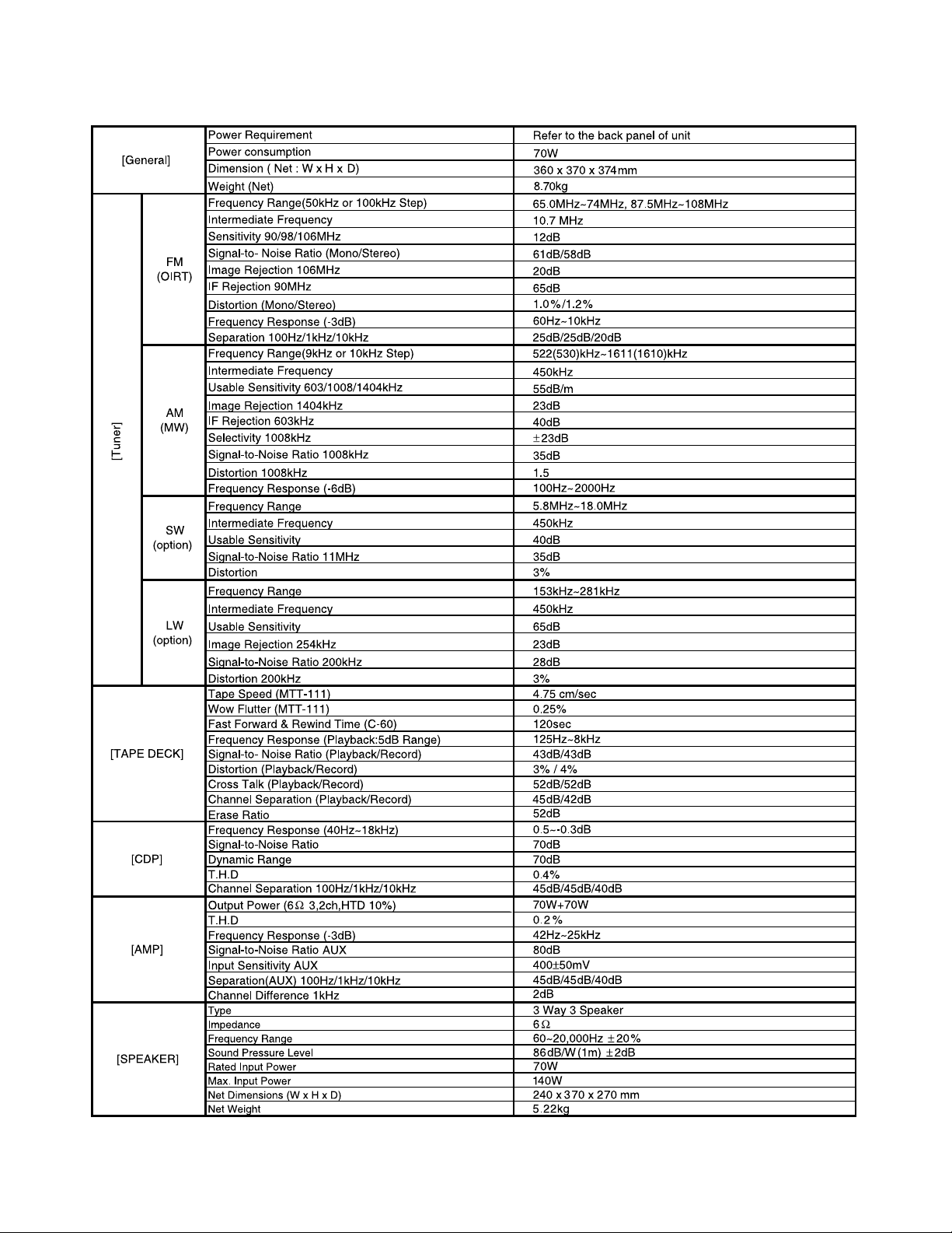
- 1-5 -
NOTE : Specification are subject to change without notice in the course of product improvement.
SPECIFICATIONS
Page 6

- 1-6 -
MEMO
Page 7
- 2-1 -
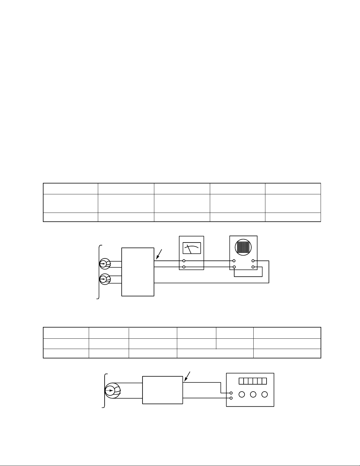
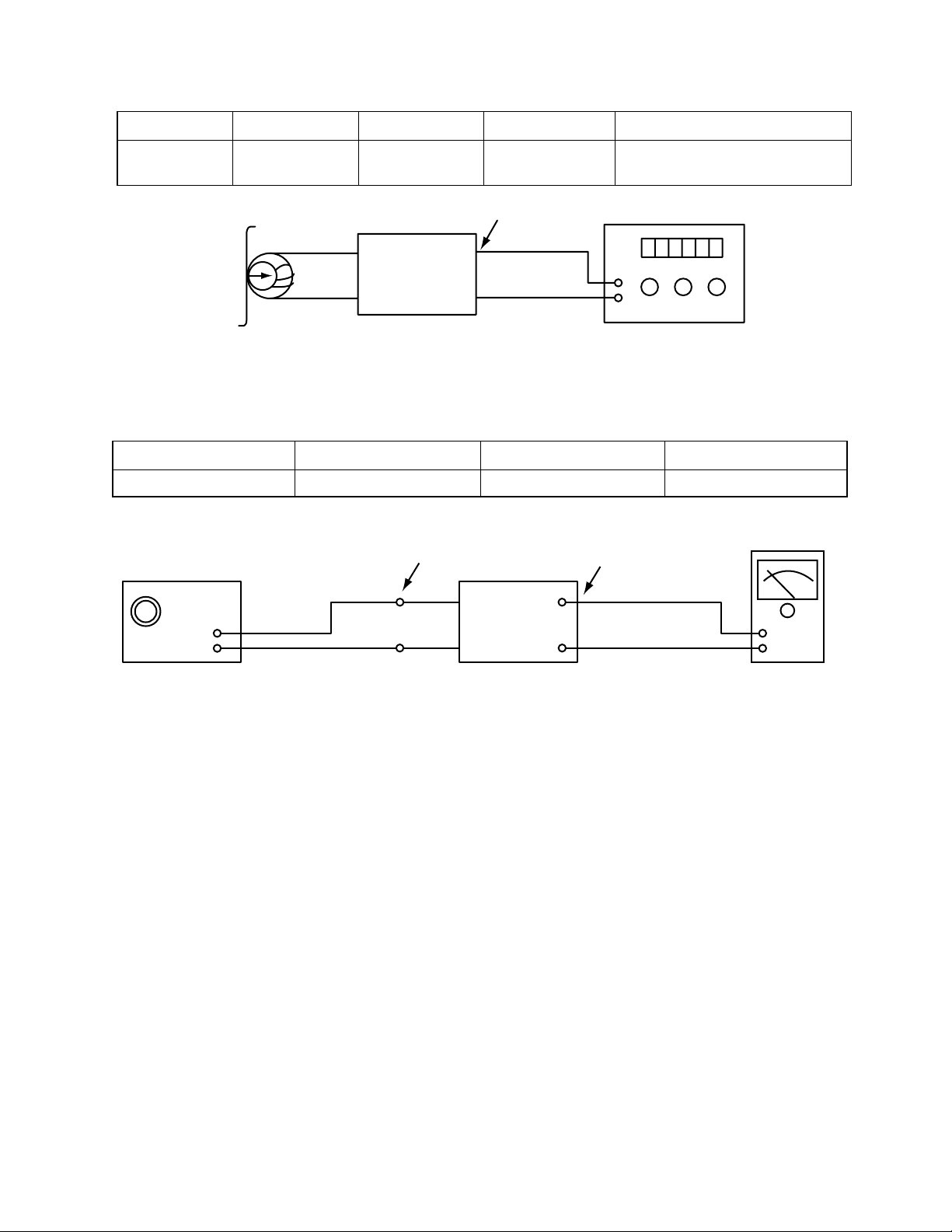
TAPE DECK ADJUSTMENT
1. AZIMUTH ADJUSTMENT
Figure 1. Azimuth Adjustment Connection Diagram
CH1 CH2
Speaker Out
Playback Mode
Head
Test Tape
MTT-114
L ch
R ch
GND
Dual-trace
synchroscope
Electronic
Voltmeter
L out
R out
Unit
SECTION 2. ELECTRICAL
ADJUSTMENTS
This set has been aligned at the factory and normally will not require further adjustment. As a result, it is not
recommended that any attempt is made to modificate any circuit. If any parts are replaced or if anyone tampers
with the adjustment, realignment may be necessary.
IMPORTANT
1. Check Power-source voltage.
2. Set the function switch to band being aligned.
3. Turn volume control to minimum unless otherwise noted.
4. Connect low side of signal source and output indicator to chassis ground unless otherwise specified.
5. Keep the signal input as low as possible to avoid AGC and AC action.
Deck Mode Test Tape Test Point Adjustment Adjust for
A Deck Playback MTT-114 Speaker Out
DECK Screw
Maximum
Azimuth Screw
B Deck Playback MTT-114 Speaker Out Azimuth Screw Maximum
2. MOTOR SPEED ADJUSTMENT
Figure 2. Motor Speed Adjustment Connection Diagram
Head
Playback Mode
Unit
Speaker Out
GND
L out
R out
Record/Playback
head
Test Tape
MTT-111
Frequency Counter
Deck Mode Test Tape Test Point Adjustment Adjust for Remark
Normal Speed MTT-111 Speaker Out VR201 3kHz ± 1% A Deck
HI-Speed MTT-111 Speaker Out more than 5.4kHz HI-Speed Dubbing Mode
Page 8
- 2-2 -
3. RECORD BIAS ADJUSTMENT
Head
Unit
PN202
GND
Record/Playback
head
Test Tape
MTT-5511
Record/Playback
and Pause Mode
Frequency Counter
Deck Mode Test Tape Test Point Adjustment Adjust for
Rec/Pause MTT-5511
ERASE HEAD
L203
60kHz±5kHz (Auto stop)
WIRE(PN202) 85kHz±5kHz(Auto Reverse)
Figure 3. Record Bias Adjustment Connection Diagram
4. TUNER ADJUSTMENT
Figure 4. Tuner(S curve) Adjustment Connection Diagram
Unit
Signal Generator
GND
Electronic
OSCILLOSCOPE
FM Antenna
Terminal
Speaker
Item Test Point Adjustment Adjust for
DC Voltage Checker IC Pin 26, 28 L106 0V±50mV
(FM)
Page 9
- 2-3 -
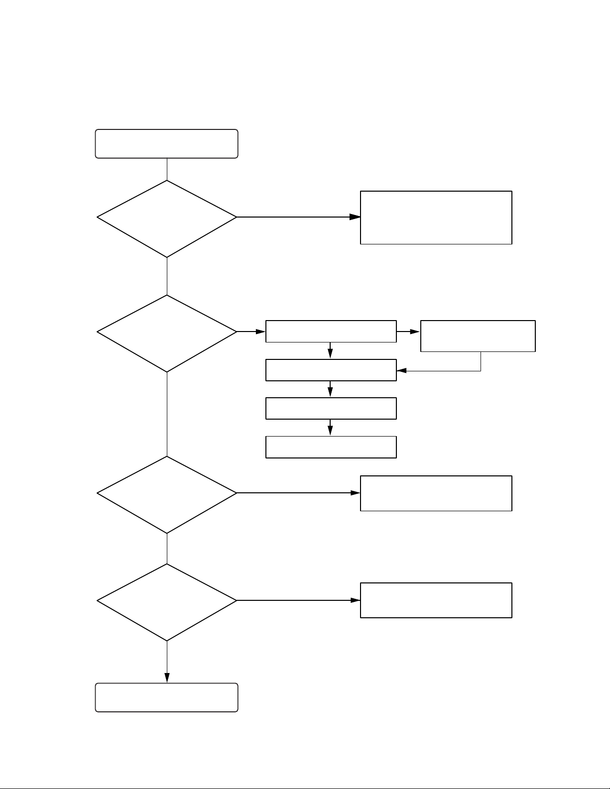
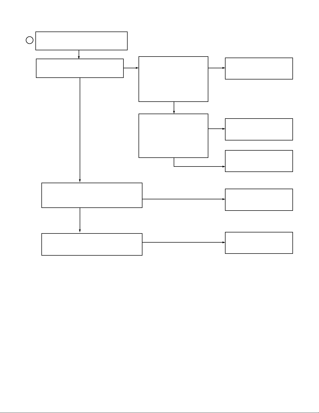
TROUBLESHOOTING
Turn power on.
Is power on?
Does initial read work?
Does it play?
Does it output audio?
Check power supply circuit.
PN807 PIN5, 6.2V
PN807 PIN7, 5V
IC803 PIN 2, 3.3V
Check the connector
PN801, PN802, PN809
Check the tracking servo circuit.
Check the PN807 PIN1, 3
OK
YES
YES
YES
YES
YES
YES
NO
NONO
Check the DISK turns
Check the Laser
Check the focus circuit
Check the TRAKING circuit
NO
NO
Page 10
- 2-4 -
Fails to initial read
A
B
2V
5V
0V
5V
0V
1V
0V
1.2V
0V
0.8V
NO NO
NO
NO
NO
NO
NO
NO
NO
NO
YES
YES
YES
YES
YES
YES
YES
YES
YES
YES
YES
YES
Disc motor turns
Does RF waveform appear?
IC801 Pin3
Check the Data transmission from
PN809 pin11 to CD DSP
Check the Data transmission from
PN809 pin13 to MICOM
Check the change of SLDO
Voltage(IC801 pin23)
Check the change of SL +,
SL - Voltage
(IC802 pin 18, 19)
Check the Voltage change of PN 809
PIN20(OPEN, CLOSE)
Defective connector
PN809
Defective connector
PN809, Defective
MICOM
Defective connector
PN809, Defective
IC801
Defective IC801
Defective IC802
Defective contact PN802
Defective PICK-UP
Does laser light?
focus coil drive wareform.
TRACKING ERROR wareform
Is rotation normal?
Defective IC801
Defective PICK-UP
Is there no dropout of RF signal?
Does FA+ waveform appear at
IC802 pin13?
Does TE waveform appear at
801 pin 15?
Page 11
- 2-5 -
NO
NO
NO
NO
NO
NO
Laser does not light.
Is “3.5V” applied to pin of IC 801?
Is power supplied to laser Q801?
(Q 801 collector: about 1.8V)
Does laser current flow?
1.0V across R808
Is data transferred from
MICOM IC ?
Does voltage appear at IC
802 pin 17, 18?
Defective MICOM.
Defective MICOM.
Defective connector.
Defective IC 801, 802
Defective slide motor and/or
connector.
Defective LMT SW and/or
connector.
Defective Q 801 and/or laser.
Defective laser and/or
connector.
Did pickup return to
innermost circular?
Does it stop at inner pick
circular after shift?
Is defect output from LM
SW applied to pin 2 of
PN802?
R808»1.0V
R808«1.0V
YES
YES
YES
YES
OPEN
CLOSE
YES
YES
YES
YES
YES
YES
70
Page 12
- 2-6 -
B
NO
NO
NO
NO
NO
YES
YES
YES
YES
Laser lights
Does lens move up/down?
Check the signal of
FOCUS SEARCH
(IC801 Pin 21)
Chekc the signal of PN802
pin 13, 14
Does FE signal appear?
(IC801 pin 13)
Does DRF signal appear? (IC 801 pin67)
Defective IC801
Defective IC802
Open activator and/or connector
Defective IC801
Degraded laser diode
Defective PICK-UP
Page 13
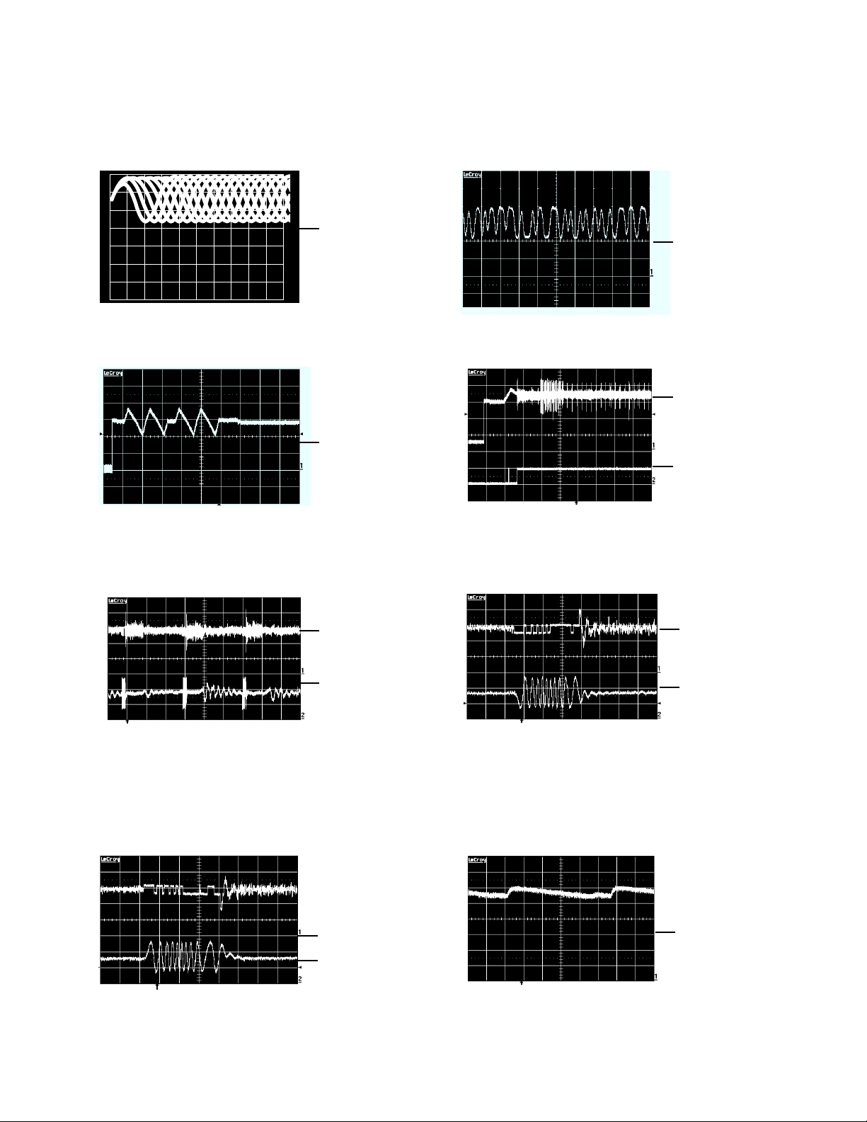
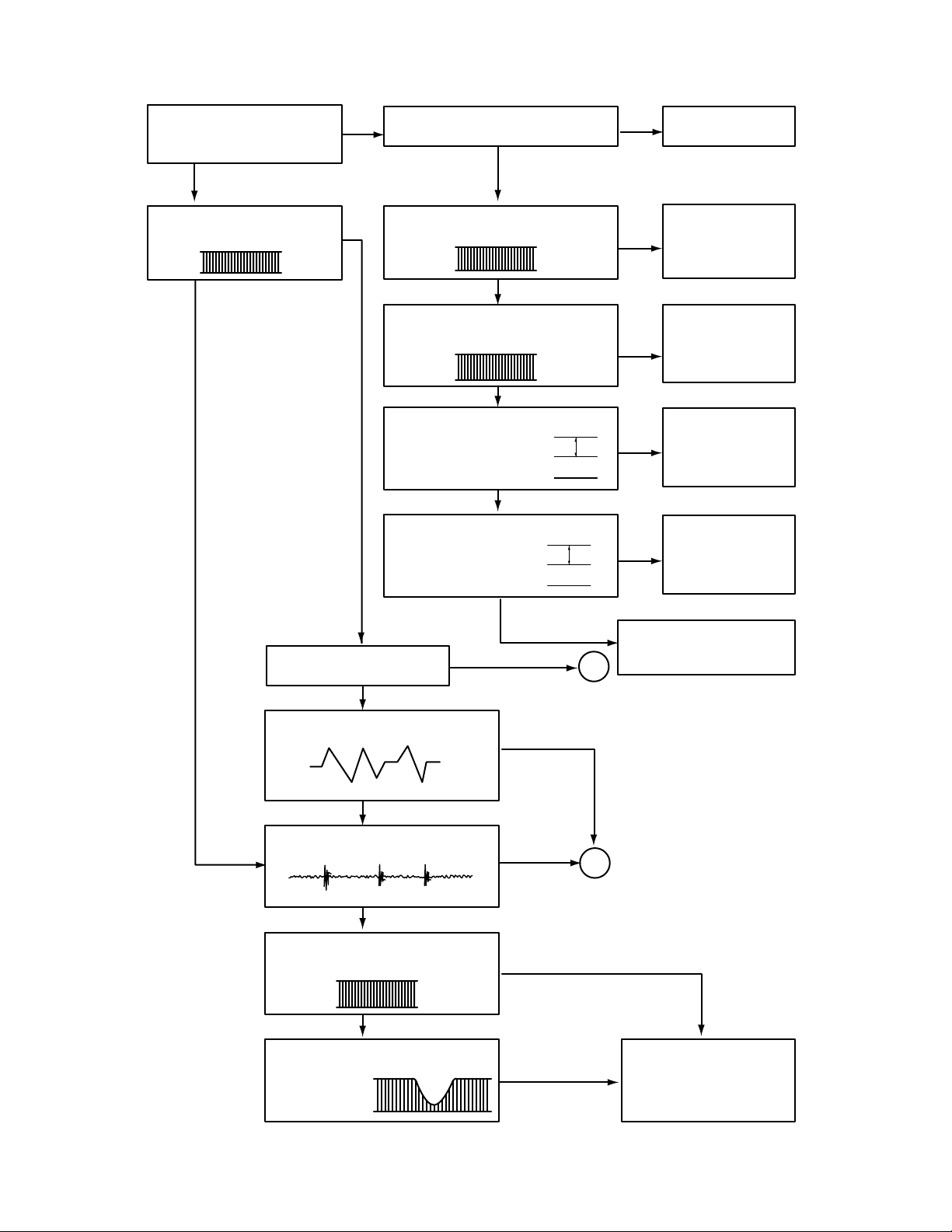
- 2-7 -
(CH1)
(CH2)
1. HF signal (RF signal ) waveform
(IC801 pin 3) during normal play
2. EFM signal (IC801 pin 3)waveform
during Normal Play
3. Focus coil drive waveform(IC802 pin13)
• When focus search failed or there is no disc on the tray
• Focus coil drive waveform(FDO: IC801 pin21) and
DRF(IC801 pin67) when focus search is accomplished
4. Tracking coil drive waveform and TE during track
traverse
(1) When time division is 20mS/Div.1V/Div.
(2) When time division 1mS/Div, 1V/Div
(During forward track traverse)
(3) When time division is 0.5nS/div.
(During backward Track Traverse)
5. Feed motor drive waveform(IC 802 pin18)
During normal play
CH1 : FOCUS COIL DRIVE
SIGNAL 2V/Div.
CH2 : DRF
CH1 : TRACKING COIL DRIVE
SIGNAL 2V/Div. (IC802 pin27)
CH2 : TRACKING ERROR(TE: IC801 pin15)
1V/Div.
(
(
(
CH2 : TRACKING COIL DRIVE (IC802 pin27)
SIGNAL 2V/Div.
CH2 : TRACKING ERROR (TE: IC801 pin15)
1V/Div.
(
CH1 : TRACKING COIL DRIVE (IC802 pin27)
CH2 : TRACKING ERROR (TE: IC801 pin15)
(
0.5V/Div.
500nS/Div.
(
1S/Div.
1V/Div.
(
1mS/Div.
1V/Div.
(
0.5V/Div.
5µS/Div.
(
2S/Div.
0.5V/Div.
OV
OV
OV
(CH1)
(CH2)
(CH1)
(CH2)
(CH2)
OV
OV
OV
OV
OV
OV
OV
OV
OV
WAVEFORMS OF MAJOR CHECK POINT
Page 14
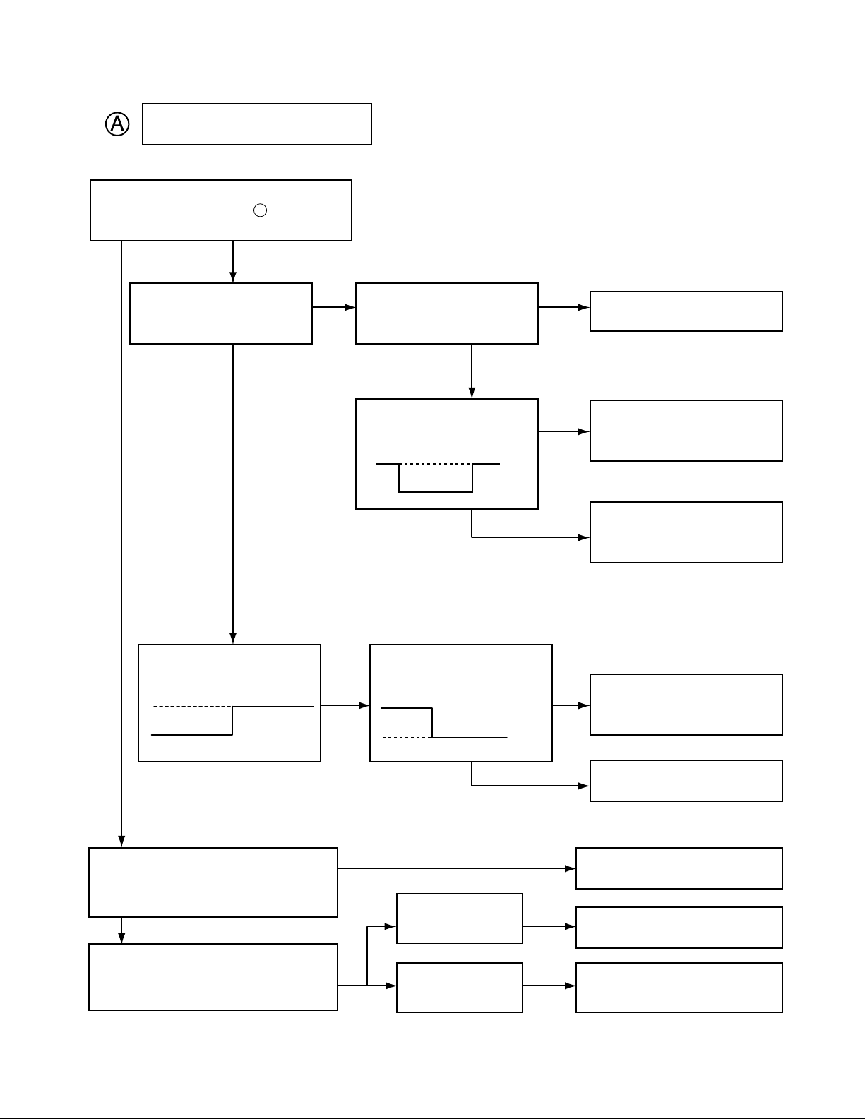
- 2-8 -
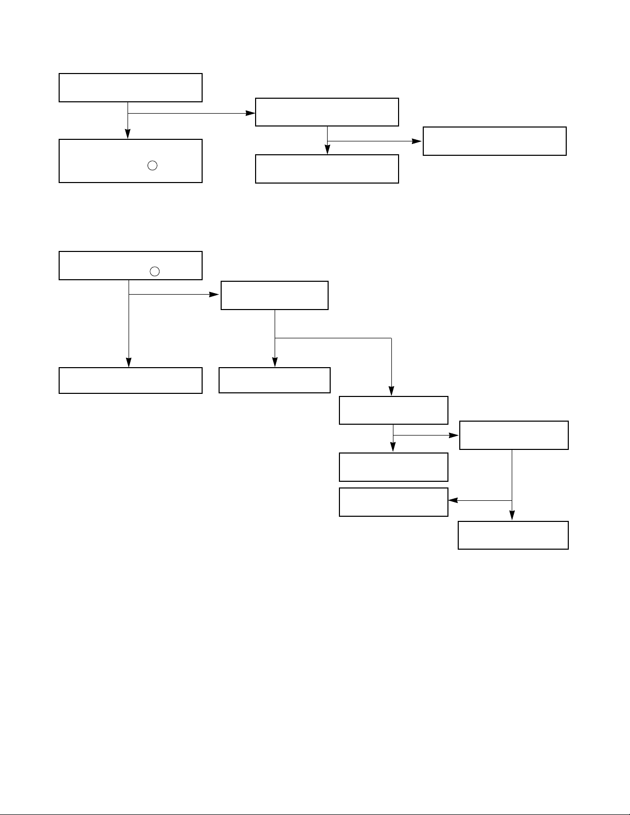
VKK PART
Does DC - 33V appear at
PN303 Pin .
OK
Dose -33V appear at
ZD702(-)
Check the Q702
TURN ON
Replace the Q702
Refer to power circuit
END
Check the -33V(LOW)
of C704(-)
Replace the D703,
D704
YES
YES
NO
NO
P-SENS PART
Does +5V appear at ZD705?
Check the pattern of
IC301 Pin .
Check the waveform
of D711(+).
Check the ZD703 or replace
Replace the D711
YES
YES
NO
NO
26
21
Page 15
- 2-9 -
Power Circuit
Muting circuit (MUTE)
Check the Fuse
Check the DC output
of C784(+), C790(-)
Check the DC Input of IC702
Check the DC
output of IC704
Check the DC 12V
Output of IC703
Check the 5V of IC704
pin 2(CD FUNCTION)
END
Dose “High” appear at
Q214, Q215, Q714, Q715
check the “LOW” Q214, Q215,
Q714, Q715 “C”
Refer to “IC202 Troubleshooting”
(ONLY Q214/Q215)
MUTE
Replace the Fuse
Check the AC Output of
CN704 pin3, 5
Check the AC Output of
CN704 PIN 7, 10
Replace the IC703
Replace the D730
Replace the
D731, D709, D710
Check the D712, D713, D714
Check the “High” of
D711(+)
Check the “High” of D714(+)
Check the “High” of Q716 “E”
(ONLY Q714/Q715)
Replace the TR
Refer the Q716
Refer to “IC301
Troubleshooting”
Replace the IC704
Replace the Transformer
Replace the Transformer
Check the Voltage of
IC301 PIN82
Refer to “IC203
Troubleshoot”
YES
YES
YES
YES
YES
YES
YES
YES
YES
YES
YES
YES
YES
NO
NO
NO
NO
NO
NO
NO
NO
NO
NO
NO
NO
NO
Page 16

- 2-10 -
Audio abnormal
SPK Relay Troubleshooting
Check the output of
IC706 Pin 9, 10
Refer to “IC701
Troubleshooting”
Refer to “Muting
Troubleshooting”
Check the power circuit
Refer to “SPK Relay
troubleshooting”
Refer to “power circuit”
Check “High” of Q709 “B”
Refer to “IC203
Troubleshooting”
Replace the RELAY(RY702)
Replace the Q709
Check the input of
IC705 IC707
Check the Input of IC707,
pin24, 25/IC705 pin 1, 7
Check the RY702
END
Check the 12V of D723(+)
Check the “Low” of Q709 “C”
Check the output
END
YES
YES
YES
YES
YES
YES
YES
YES
NO
NO
NO
NO
NO
NO
NO
NO
Page 17

- 2-11 -
FUNCTION MODE Audio abnormal
TAPE
Check the signal input of IC707 pin 28, 37
Refer to “IC202 Troubleshooting”
AUX
Chekc the signal input of IC707, pin 29, 36
Check the signal input of JK102
Check the signal input of IC707 pin 31, 34
Refer to “CD Troubleshooting”
Check the signal input of IC707 pin 30, 35
Refer to “IC102 Troubleshooting”
CD
Tuner
Page 18

- 2-12 -
Refer to “IC301
Troubleshooting”
IC301 Troubleshooting
IC203, IC302 Troubleshooting
Check the power supplying IC301 Pin 17, 46, 90?
Refer to “Power Circuit Troubleshooting”
Check the P-SENS
Replace the X301
Check the RESET circuit
Refer to “Power Circuit Troubleshooting”
Check the Data of IC301 Pin 3, 4, 5
(CD ➞ TAPE FUNCTION)
Replace the
IC501/IC302
Check the pattern
of (IC301, IC203, IC302)
Check the 5v of IC301 pin26
Check the oscillation of X301
When power supplying to IC301 pin17.
(Low ➞ High)
Replace the IC301
Check the power supplying to IC203/IC302 pin 16
Check the CLK Data of IC203/IC302 pin 2, 3
Check the CONTROLL function
END
YES
YES
YES
YES
YES
YES
YES
NO
NO
NO
NO
NO
NO
NO
Page 19

- 2-13 -
IC601 Troubleshooting
Refer to “Power circuit Troubleshooting”
Refer to “FUNC Troubleshooting”
Refer to “SPK Relay”
Check the FUNC CLOCK DATA of pin 21, 22
Check the power of pin 39
Check the signal input
Check the Signal output of pin25, 24
OK
YES
YES
YES
YES
NO
NO
NO
FM (TUN101)
Check the 12V input of TUN101 B+ 6
Check the “High” Voltage of TUN101 VT 5
Check the OSC waveform of TUN101 Pin 8
Refer to “IC102 Troubleshooting”
Check the 12V of Q102 “E”
Refer to “Power
Circuit Trouble-
shooting”
Check the “GND” of IC103 Pin 7
Refer to “IC103
Troubleshooting”
Replace the Q102
Replace the TUN101
Replace the TUN101
YES
YES
YES
YES
YES
NO
NO
Page 20

- 2-14 -
IC102 Troubleshooting
Is power supplied to pin8
Check the waveform of Pin 20, 21
Check the output of Pin 16, 17
END
Refer to “Power Circuit
Troubleshooting”
Check the FM(TUN101) & AM(L107)
Replace the IC102
Replace the IC102
Check the “Low” of Pin 13
Refer to “IC103
Troubleshooting”
YES
YES
YES
YES
NO
NO
NO
NO
NO
IC103 Troubleshooting
Check the power supplying to pin 17
Check the oscillation of X104
Check the waveform of CE, DI, DO, CLK
Is the normal ?
END
Refer to “Power Circuit
Troubleshooting”
Replace the X104
Check the line or refer to “IC 301
Troubleshooting”
CE: Chip Enable
DI: Data Input(from u-com)
DO: Data Output(to u-com)
CLK: Tuner mode clock
Replace the IC103
YES
YES
YES
YES
NO
NO
NO
NO
Page 21

- 2-15 -
AM•COIL Troubleshooting
Check the “High” of L107 Pin 2
Refer to “IC103 Troubleshooting”
Replace the L107
Check the oscillation of L107 Pin 13
Refer to “IC102 Troubleshooting”
YES
YES
NO
NO
Play
Check the VCC supplying to IC202 pin 18
Refer to “Power Circuit Troubleshooting”
Check the Deck Mecha
Replace the Deck
Mecha.
Replace the IC202
Check the signal output of IC202 pin 5, 20
Check the Muting Circuit
YES
YES
YES
NO
NO
NO
YES
YES
NO
Dubbing(“NORMAL or REC “//“HIGH”)
Q209, 212 “OFF”//“ON” : R273, 223
“LOW”//“HIGH
Q253, 203 “ON”//“OFF” : R225, 275
“High”//”Low”
Refer to “IC203 Troubleshooting”
Refer to “REC Troubleshooting”
Page 22

- 2-16 -
REC (Q252, Q202 ON / R273, R223 High)
Check signal supplied to IC202 pin 11, 14?
Check the output of IC202 Pin9, 16
Check the IC201 pin6 : 12V and pin 4 : High
Check the power or Refer to “IC203
Troubleshooting”
Check the power
supplying to C236(+)
Check the 0.6V of Q208
“B”
Check the “Low” of
Q208 “C”
Replace the Q207
END
Check the Vcc power of IC202 Pin18
Check the oscillation of L203 pin 2, 3
Replace the DECK
Check the “Low” of Q210,
Q211 “B”
Replace the Q210, Q211
Refer to “IC203
Troubleshooting”
Refer to “Power Circuit
Troubleshooting”
Refer to “IC203
trouleshooting”
Replace the Q208
Replace the L203
YES
YES
YES
YES
YES
YES
YES
YES
YES
NO
NO
NO
NO
NO
NO
NO
NO
NO
Page 23

- 2-37 -
• Power P.C. BOARD
Page 24

- 2-38 -
• CD MAIN P.C. BOARD
Page 25

- 2-39 -
INTERNAL BLOCK DIAGRAM OF ICs
■ FAN8039BD3
5-CH Motor Diver
Description
The FAN8039BD3 is a monolithic integrated circuit suitable for a 5-CH motor driver which drives the
tracking actuator, focus actuator, sled motor, tray motor, spindle motor of the DVDP/CAR-CD systems.
28
2627
25 24 23 22
1 32 4 5 6 7
211920 18
17
16 15
8109
11
12
13 14
DO1-
DO
1+
IN1
REGVCC
REB
REO
RESX
GND1
FWD
IN2
DO2+
DO2-
GND2
REV
DO5+
DO 5-
DO3-
DO 3
+
IN3
CTL
VCC1
VCC
VREF
PS
IN4
DO 4+
DO4
-
GND3
TSD
10K
10K
10K
10K
2.5V
Regulator
Level
Shift
Level
Shift
COMP
2
2
2 2
2 2
FIN
(GND)
FIN
(GND)
Level
Shift
Level
Shift
10K
10K
Level
Shift
2
2
PS
RESX
FUNCTION
H
H
H
L
L
H
L
L
All Active
Reg. Only Deactive
Reg. Only Active
All Deactive
Pin Definitions
NO Symbol Description NO Symbol Description
1DO1-CH1 Drive Output (-) 15 GND2 Power Ground1 (CH 2,3,5)
2DO1+CH1 Drive Output (+) 16 DO5+ CH5 Drive Output (+)
3IN1 CH1 Drive Input 17 DO5- CH5 Drive Output(-)
4REGVCC Regulator Supply Voltage 18 DO3- CH3 Drive Output(-)
5REB Regulator Output 19 DO3+ CH3 Drive Output (+)
6REO Regulator Feedback Input 20 IN3 CH3 Drive Input
7RESX Regulator Reset 21 VCC1 Supply Voltage1(CH2,CH3,CH5)
8GND1 Signal Ground 22 PS Power Save
9CTL CH5 Motor Speed Control 23 VREF Bias Voltage
10 FWD CH5 Forward Input 24 VCC Supply Voltage(CH1,CH4)
11 REV CH5 Reverse Input 25 IN4 CH4 Drive Input
12 IN2 CH2 Drive Input 26 DO4+ CH4 Drive Output (+)
13 DO2+ CH2 Drive Output (+) 27 DO4- CH4 Drive Output (-)
14 DO2- CH2 Drive Output (-) 28 GND3 Power Ground2 (CH 1,4)
Page 26

- 2-40 -
■ KA78R33
Low Dropout Voltage Regulator
Description
The KA78R33 is a low-dropout voltage regulator suitable for various electronic equipments. It provides
constant voltage power source with TO-220 4 lead full mold package. Dropout voltage of KA78R33 is
below 0.5V in full rated current(1A). This regulator has various function such as peak current protection,
thermal shut down, overvoltage protection and output disable function.
Internal Block Diagram
THERMAL SHUTDOWN
BANDGAP REFERENCE
OVERVOLTAGE
PROTECTION
SOA PROTECTION
SHORTCIRCUIT
PROTECTION
1
4
3
2
Vin
Vdis
Vo
GND
HIGH / LOW
OUTPUT
ON / OFF
Q1
R1
R2
-
+
+
1.4V
-
CIRCUIT
■ LC72131
AM/FM PLL Frequency Synthesizer
Page 27

- 2-41 -
B01 B02 B03 B04 I01 I02
XIN
PD
AIN
AOUT
IFIN
XOUT
FMIN
AMIN
CE
DI
CL
D0
VDD
VSS
REFERENCE
DIVIDER
PHASE DETECTOR
CHARGE PUMP
UNLOCK
DETECTOR
UNIVERSAL
COUNTER
DATA SHIFT REGISTER
LATCH
12bits PROGRAMMABLE
DIVIDER
SWALLOW COUNTER
1/16. 1/17 4bits
POWER
ON
RESET
CCB
I/F
1
2
Block Diagram
■ LA1837
Single-Chip Home stereo IC with Electronic Tuning Support
The LA1837 is a single-chip AM/FM IF and MPX IC that supports electronic tuning and was developed for
use in home stereo systems. It is optimal for use in automatic station selection systems that use the SD and
IF counting techniques.
Block Diagram
FM SD
ADJ
3 rd 5 th
DECODER
ANTI-BIRDIE
FM
Page 28

- 2-42 -
■ KIA 78R12 PI
4 TERMINAL LOW DROP VOLTAGE REGULATOR
The KIA78RXX Series are Low Drop Voltage Regulator suitable for various electronic equipments. It
provides constant voltage power source with TO-220 4 termainal lead full molded PKG. The Regulator has
multi function such as over current protection, overheat protection and ON/OFF control.
Page 29

- 2-43 -
■ KIA7805AP/API
THREE TERMINAL POSITIVE VOLTAGE REGULATORS 5V, 6V, 8V, 9V, 10V, 12, 15V, 18V, 24V.
EQUIVALENT CIRCUIT
Block Diagram
Page 30

- 2-44 -
■ BA3126N
2-channel head switch for radio cassette recorders
Page 31

- 2-45 -
Control circuit
12-bit shift register
Latch
Output buffer
(open drain)
1Vss
2DATA
3CLOCK
4Q0
5Q1
6 Q2
7Q3
8Q4
16 VDD
15 Q11
14 Q10
13 Q9
12 Q8
11 Q7
10 Q6
9 Q5
Pin No.
Pin name Function
BU2090/F/FS BU2092/F BU2092/FV
111Vss GND
222DATA Serial data input
333CLOCK Data shift clock input
-44LCK Data latch clock input
455Q0parallel data output
566Q1parallel data output
677Q2parallel data output
788Q3parallel data output
899Q4parallel data output
91010Q5parallel data output
10 11 11 Q6 parallel data output
--12 N.C. Not connected
--13 N.C. Not connected
11 12 14 Q7 parallel data output
12 13 15 Q8 parallel data output
13 14 16 Q9 parallel data output
14 15 17 Q10 parallel data output
15 16 18 Q11 parallel data output
-1719OEOutput Enable
16 18 20 V
DD Power supply
PIN DESCRIPTION
■ BU2090F
12-bit, Serial IN, Parallel OUT driver
Block diagram
Page 32

- 2-46 -
REPAIRS REGARDING CD MECHANISM
IMPROVED METHOD - WHEN THE TRAY GEARS WERE DISTORTED
1. How to open the tray.
In case of not suppling power push two hooks (H) of the base, and them open the tray.
2. How to improve the distorted gears.
(1) Do the hole "C" of the cam gear to face forward the pick-up so the pick-up is down like figure.
(2) Do the hole "B" of main gear to face forward pick-up, too.
(3) Set the last part of main gear to point "A".
(4) Push the tray to end.
Page 33

- 4-1 -
SECTION 4. SPEAKER SECTION
MODEL: FE-5670E
851
852
862
853
861
861
854
855
856
857
858
861
LOCA.NO. PART NO DESCRIPTION SPECIFICATION REMARKS
851 3720RMF022A PANEL,FRONT FRONT FE-5670E SILVER
852 6400RMEB01A SPEAKER,TWEETER FE-876E 06N39EHC0339A EAW 6OHM
853 6400RCEY01A SPEAKER,FULLRANGE 6400RCEY01A EAW 500 OHM 100 W
854 6400SCEJ02K SPEAKER,WOOFER 16LA0EHC1348G EAW WOOFER 5670E
856 4766RM0019B FELT FE-886E BLACK DUCT
857 3091RMW033A CABINET ASSEMBLY FE-5670E CABINET(195MM, PB12T)
858 6871RU9244A PWB(PCB) ASSEMBLY,SUBSET(AUDIO FE-5670E NETWORK ASSY
861 353M050C SCREW BH 3.5X16 FBK
862 353M025F SCREW TAPTITE, 3X8 FZMY
RUN DATE : 14.AUGUST.2002
Page 34

- 4-2 -
MEMO
Page 35

2-17 2-18
BLOCK DIAGRAM
NOTE: Warning
Parts that are shaded are critical With respect
to risk of fire or electrical shock.
NOTE:
1. Shaded(■) parts are critical for safety.Replace only
with specified part number.
2. Voltages are DC-measured with a digital voltmefer
during Play mode.
Page 36

SCHEMATIC DIAGRAMS
• MAIN SCHEMATIC DIAGRAM
2-19 2-20
NOTE: Warning
Parts that are shaded are critical With respect
to risk of fire or electrical shock.
NOTE:
1. Shaded(■) parts are critical for safety.Replace only
with specified part number.
2. Voltages are DC-measured with a digital voltmefer
during Play mode.
Page 37

2-21 2-22
• FRONT SCHEMATIC DIAGRAM
Page 38

2-23 2-24
• TUNER/DECK SCHEMATIC DIAGRAM
Page 39

2-25 2-26
• CDP SCHEMATIC DIAGRAM
Page 40

2-27 2-28
WIRING DIAGRAM
NOTE: Warning
Parts that are shaded are critical With respect
to risk of fire or electrical shock.
Page 41

2-29 2-30
PRINTED CIRCUIT DIAGRAMS
• MAIN P.C. BOARD (SOLDER SIDE)
Page 42

2-31 2-32
• MAIN P.C. BOARD (COMPONENT SIDE)
Page 43

2-33 2-34
• FRONT P.C. BOARD(COMPONENT SIDE)
Page 44

2-35 2-36
• FRONT P.C. BOARD(SOLDER SIDE)
Page 45

SECTION 3. EXPLODED VIEWS
• CABINET AND MAIN FRAME SECTION
351
301
305
A47
302
303
306
354
458
451
354
458
A41
294
291
292
454
285
A43
A00
272
287
286
276
278
277
275
264
295
296
297
262
260
289
250
271
273
274
293
265
284
(Option)
A46
FAN
257
A26
456
NOTE) Refer to “SECTION 5 REPLACEMENT
PARTS LIST” in order to look for the
part number of each part.
3-1 3-2
Page 46

3-3 3-4
• TAPE DECK MECHANISM: AUTO STOP DECK(OPTIONAL)
400
011
503
401
401
009
010
501
502
013
406
409
408
407
032
031
030
029
028
401
027
026
014
015
403
504
024
025
023
405
A01
402
022
016
017
018
019
020
021
505
007
008
003
004
005
001
002
404
400
400
006
LOCA. NO PART NO. SPECIFICATION
A00 6730R-G007A CWL44FF25 TOKYO PIGEON L-DOUBL
A01 6768R-UP01A 50-093-4249 PIGEON UNIT PCB AS
001 6768R-BP01B 02-084-4202 PIGEON BELT / FELT C
002 6768R-BP01A 02-084-4204 PIGEON BELT / FELT C
003 6768R-AP01D 50-239-4027 PIGEON ARM CWL44
004 6768R-AP01E 50-239-4026 PIGEON ARM CWL44
005 6768R-SP01E 01-082-4599 PIGEON SPRING CWL4
006 6768R-QP01A 50-093-4316 PIGEON MOTOR(ASSY)
007 6768R-GP01A 50-093-4063 PIGEON GEAR CWL44
008 6768R-SP01F 01-082-4598 PIGEON SPRING CWL4
009 6768R-MP01C 50-219-4014 PIGEON MOLD CWL44
010 6768R-SP01C 01-082-4652 PIGEON SPRING CWL4
011 6768R-SP01A 01-081-4601 PIGEON SPRING CWL4
013 6768R-SP01B 01-082-4651 PIGEON SPRING CWL4
014 6768R-SP01G 01-082-4597 PIGEON SPRING CWL4
015 6768R-AP01A 50-268-3016 PIGEON ARM CWL44
016 6768R-GP01C 50-093-4069 PIGEON GEAR CWL44
017 6768R-AP01C 50-239-4072 PIGEON ARM CWL44
018 6768R-GP01D 50-222-4007 PIGEON GEAR CWL44
019 6768R-SP01H 01-081-4657 PIGEON SPRING CWL4
020 6768R-BP01C 02-083-4188 PIGEON BELT / FELT C
021 6768R-LP01A 50-223-4254 PIGEON PULLEY / FLYW
022 6768R-VP01A 50-093-4125 PIGEON SOLENOID CW
023 6768R-GP01B 50-221-3009 PIGEON GEAR CWL44
024 6768R-AP01B 50-139-4292 PIGEON ARM CWL44
025 6768R-JP01B 50-093-3361 PIGEON PULLEY / FLYW
026 6768R-SP01D 01-080-4609 PIGEON SPRING CWL4
027 6768R-MP01B 50-093-3036 PIGEON MOLD CWL44
028 6768R-RP01A 22-027-41054 PIGEON ROLLER CWL
029 6768R-MP01A 50-219-4033 PIGEON MOLD CWL44
030 6768R-HP01A TC881CB067B PIGEON HEAD CWL44
031 6768R-SP01J 01-081-4605 PIGEON SPRING CWL4
032 6768R-HP01B TC231F PIGEON HEAD CWL44
033 6768R-JP01A 50-093-3360 PIGEON PULLEY / FLYW
400 6768R-CP01A GSE10A2003 PIGEON SCREW CWL44
401 6768R-CP01B GSE20A2005 PIGEON SCREW CWL44
402 6768R-CP01C GSE10A2004 PIGEON SCREW CWL44
403 6768R-CP01D GSL10A1704 PIGEON SCREW CWL44
404 6768R-CP01E GSP10A2603 PIGEON SCREW CWL44
405 6768R-CP01F GSP11A2012 PIGEON SCREW CWL44
406 6768R-CP01G GSE20A2004 PIGEON SCREW CWL44
407 6768R-CP01H GSL20A2005 PIGEON SCREW CWL44
408 6768R-CP01J 03-300-4127 PIGEON SCREW CWL44
409 6768R-CP01K GSL20A2008 PIGEON SCREW CWL44
501 6768R-WP01A GWM19S035035 PIGEON WASHER CWL
502 6768R-WP01B GWM17S050035S PIGEON WASHER CW
503 6768R-WP01C GWM40X075010 PIGEON WASHER CWL
504 6768R-WP01D GWP21X045020 PIGEON WASHER CWL
505 6768R-WP01E GWP12X030040S PIGEON WASHER CW
Page 47

3-5 3-6
• TAPE DECK MECHANISM: AUTO REVERSE DECK
400
011
503
401
401
009
010
501
502
507
508
013
406
409
410
036
032
038
034
035
039
029
040
031
028
027
026
014
015
403
504
024
025
023
405
A01
402
022
016
017
018
019
020
021
505
007
008
003
004
005
001
002
404
400
400
506
037
006
LOCA. NO PART NO. SPECIFICATION
A00 6730R-G007B CDM-H1323 CD CHAN
A01 6768R-UP01A 50-093-4249 PCB AS
001 6768R-BP01B 02-084-4202 BELT/FELT
002 6768R-BP01A 02-084-4204 BELT/FELT
003 6768R-AP01D 50-239-4027 CWL44
004 6768R-AP01E 50-239-4026 ARM
005 6768R-SP01E 01-082-4654 SPRING
006 6768R-QP01A 50-093-4316 MOTOR
007 6768R-GP01A 50-093-4063 GEAR
008 6768R-SP01F 01-082-4598 SPRING
009 6768R-MP01C 50-219-4014 MOLD
010 6768R-SP01C 01-082-4652 SPRING
011 6768R-SP01A 01-081-4601 SPRING
013 6768R-SP01B 01-082-4651 SPRING
014 6768R-SP01G 01-082-4597 SPRING
015 6768R-AP01A 50-268-3016 ARM
016 6768R-GP01C 50-093-4069 GEAR
017 6768R-AP01C 50-239-4072 ARM
018 6768R-GP01D 50-222-4007 GEAR
019 6768R-SP01H 01-081-4657 SPRING
020 6768R-BP01C 02-083-4188 BELT/FELT
021 6768R-LP01A 50-223-4254 PULLEY
022 6768R-VP01A 50-093-4125 SOLENOID
023 6768R-GP01B 50-221-3009 GEAR
024 6768R-AP01B 50-139-4292 ARM
025 6768R-JP01B 50-093-3361 PULLEY
026 6768R-SP01D 01-080-4609 SPRING
027 6768R-DP01A 50-259-3342 LEVER
028 6768R-RP01A 22-027-41054 ROLLER
029 6768R-MP01A 50-219-4033 MOLD
031 6768R-SP01L 01-080-4649 SPRING
032 6768R-EP01A 50-093-4070 HEAD AY
033 6768R-JP01A 50-093-3360 PULLEY
034 6768R-SP01K 01-082-4650 SPRING
035 6768R-PP01A 50-119-4046 PRESS
036 6768R-PP01B 50-160-4108 PRESS
037 6768R-JP01C 50-093-3315 PULLEY
038 6768R-MP01D 50-219-4034 MOLD
040 6768R-SP01M 01-080-4607 SPRING
400 6768R-CP01A GSE10A2003 SCREW
401 6768R-CP01B GSE20A2005 SCREW
402 6768R-CP01C GSE10A2004 SCREW
403 6768R-CP01D GSL10A1704 SCREW
404 6768R-CP01E GSP10A2603 SCREW
405 6768R-CP01F GSP11A2012 SCREW
406 6768R-CP01G GSE20A2004 SCREW
409 6768R-CP01L GSD10A2018 SCREW
410 6768R-CP01M 03-300-4056 SCREW
501 6768R-WP01A GWM19S035035 WASHER
502 6768R-WP01B GWM17S050035S WASHER
503 6768R-WP01C GWM40X075010 WASHER
504 6768R-WP01D GWP21X045020 WASHER
505 6768R-WP01E GWP12X030040S WASHER
506 6768R-WP01H GWP23X040020 WASHER
507 6768R-WP01F GWN21X040040 WASHER
508 6768R-WP01G GWM19X055035S WASHER
Page 48

3-7 3-8
• CD MECHANISM
416
151
152
155
184
185
184
A35
421
A30
421
168
417
417
153
159
A26
169
154
158
157
156
418
416
419
165
162
166
420
167
177
176
164
163
175
170
171
174
416
173
172
417
LOCA.NO. PART NO DESCRIPTION SPECIFICATION
A26 4405RBE003F MECHANISM ASSEMBLY CDM-H133 LGEHZ 3 CD CHANGER (S
A30 3041RB0002C BASE ASSEMBLY PU(SPRING DAMPER)
A35 6717RCA001A PICK UP ASSY KSM-213VSCM SONY FRONT LOADING
151 3390SB0002A TRAY DISC (CDM-H1303)
152 4470SB0011A GEAR TRAY B (CDM-H1303)
153 4470SB0010A GEAR TRAY A (CDM-H1303)
154 4400SB0001B BELT TRAY(CDM-H1303)
155 4680SBP002A MOTOR(MECH) ASSY TRAY
156 6871SF21RAD PWB(PCB) ASSY 3CH M/D SENSOR PWB ASSY
157 4974SB0003A GUIDE WORM (CDM-H1303)
158 4371SB0002A SHAFT ASSY TRAY (CDM-H1303)
159 3390SB0001A TRAY LOADING (CDM-H1303)
162 4400SB0001A BELT MAIN(CDM-H1303)
163 4470SB0003A GEAR PULLEY (CDM-H1303)
164 4470SB0004A GEAR LOADING (CDM-H1303)
165 6871SB21RAD PWB(PCB) ASSY 3CH M/D U/D/O/C PWB ASSY
166 4470SB0006A GEAR PU DOWN (CDM-H1303)
167 4470SB0008A GEAR PU UP-B (CDM-H1303)
168 4471SB0001A GEAR ASSY GEAR CAM ASSY
169 4860SB0002A CLAMP CLAMP ASSY
170 4974SB0001A GUIDE CAM (CDM-H1303)
171 4970SBN002A SPRING CAM (CDM-H1303)
172 3040SB0002A BASE MAIN(CDM-H1303)
173 6871SD21RAD PWB(PCB) ASSY 3CH M/D CAM PWB ASSY
174 6871SC21RAD PWB(PCB) ASSY 3CH M/D OPEN PWB ASSY
175 4680SBP001A MOTOR(MECH) PULLEY ASSY (CDM-H1303)
176 4470SB0007A GEAR PU UP-A (CDM-H1303)
177 4470SB0005A GEAR MAIN (CDM-H1303)
184 4900RB0001A DAMPER RUBBER 3CD CHANGER
185 3040SB0003A BASE PU(CDM-H1303)
186 4970RB0001A SPRING COIL 3 CD CHANGER
187 4970RB0001B SPRING COIL 50 3CD CHANGER
416 88H-0004 CD MECHA PARTS 3X12X12FNM
417 88H-0002 CD MECHA PARTS 3X9X12FZMY
418 353-025BAAA SCREW #NAME?
419 88H-0003 CD MECHA PARTS 3X12X10FZMY
420 353S353F SCREW #NAME?
421 6756SBX001A CD MECHANISM PARTS SCREW 2.6X10X10XFZMY CDM-H813
 Loading...