LG FB915BU Service Manual
Service Guide Specification
Service Guide Specification
Model Description
1.
MODEL
SUFFIX
2.
F920BJ
ALEUQ
BRAND
Product Name
Printing Specification
1. Trim Size (Format) : 215mm x 280 mm
2. Printing Colors
• Cover : LG COLORS
• Inside : Black
3. Stock (Paper)
• Cover : Snow White 150 g/
• Inside : Snow White 100 g/
4. Printing Method :
5. Bindery : Saddle stitch
6. Language : English
7. Number of pages : 52 ( Including blank 3page)
LG
FLATRON F920B
Part No.
3828TSL087F
Special Instructions3.
(1) Origin Notification
* LGEDI : Printed in Indonesia * LGEWA : Printed in U.K.
* LGESP : Printed in Brazil * LGEMX : Printed in Mexico
* LGENT : Printed in China * LGEIL : Printed in India
4.
Changes
8
7
6
5
4
3
2
1
REV.
MM/DD/YY
NO.
CHANGE NO.
CHANGE CONTENTS
Pagination sheet
Pagination sheet
Cover
English
2
English
44
English
3
Blank
English
4
Blank
English
5
2 2
45 34
English
….
English
…..
English
PCB 2
47 48
English
42
43
Rear
Cover
Inside
Blank
Rear
Cover
COLOR MONIT OR
SER VICE MANUAL
Website:http://biz.LGservice.com
E-mail:http://www.LGEservice.com/techsup.html
CAUTION
BEFORE SERVICING THE UNIT,
READ THE SAFETY PRECAUTIONS IN THIS MANUAL.
MODEL: F920B (F920BJ-AL**Q)
CHASSIS NO. : CA-130
( ) **Same model for Service
1. PICTURE TUBE
Size : 19 inch (Flat Slot Mask)
DefIection Angle : 90°
Neck Diameter : 29.1 mm
Strip Pitch : 0.24 mm
Diagonal Size : 457.5 mm
View Size : 366.0 x 274.5 mm
Face Treatment : AR-ASC (Anti-Reflective and
Anti-Static Coating)
2. SIGNAL
2-1. Horizontal & Vertical Sync
1) Input Voltage Level: Low= ≤0.8V, High= ≥2.1V
2) Sync Polarity : Positive or Negative
2-2. Video Input Signal
1) Voltage Level : 0~0.7 Vp-p
a) Color 0, 0 : 0 Vp-p
b) Color 7, 0 : 0.467 Vp-p
c) Color 15, 0 : 0.7 Vp-p
2) Input Impedance : 75 Ω
3) Video Color : R, G, B Analog
4) Signal Format : Refer to the Timing Chart
2-3. Signal Connector
15 Pin D-Sub Connector
2-4. Scanning Frequency
Horizontal : 30~98 kHz
Vertical : 50~160 Hz
3. POWER SUPPLY
3-1. Power Range
AC 100-240V~50/60HZ, 2.5A Max
AC 200-240V~50Hz, 1.5A Max.(PFC version)
3-2. Power Consumption
4. DISPLAY AREA
4-1. Active Video Area :
• Max Image Size - 366.0 x 274.5mm (14.40" x 10.80")
• Preset Image Size - 350 x 262 mm (13.78" x 10.31")
4-2. Display Color : Full Colors
4-3. Display Resolution : 1600 Dots x 1200Lines/75Hz
4-4. Video Bandwidth : 203MHz
5. ENVIRONMENT
5-1. Operating Temperature: 0°C~40°C (32°F~103°F)
(Ambient)
5-2. Relative Humidity : 10%~90%
(Non-condensing)
5-3. Altitude : 10,000 ft
6. DIMENSIONS (with TILT/SWIVEL)
Width : 466.6 mm (18.37")
Depth : 472.5 mm (18.60")
Height : 474 mm (18.66")
7. WEIGHT (with TILT/SWIVEL)
Net Weight : 23.2 kg (51.82 lbs)
Gross Weight : 26.6 kg (59.52 lbs)
8. USB Specifications
USB Standard :
Rev. 1.0 complied self-powered hub
Downstream power supply
: 500mA for each (MAX)
Communication speed : 12 Mbps (Full), 1.5 Mbps (Low)
USB port : 1 Upstream port
2 Downstream ports
CONTENTS
SPECIFICATIONS
- 2 -
SPECIFICATIONS ................................................... 2
SAFETY PRECAUTIONS ........................................ 3
SERVICE PRECAUTIONS ...................................... 4
TIMING CHART ....................................................... 7
DISASSEMBLY ....................................................... 8
ADJUSTMENT ........................................................ 9
WIRING DIAGRAM ............................................... 15
BLOCK DIAGRAM ................................................. 16
DESCRIPTION OF BLOCK DIAGRAM...................17
TROUBLESHOOTING GUIDE .............................. 19
EXPLODED VIEW.................................................. 36
REPLACEMENT PARTS LIST ...............................38
SCHEMATIC DIAGRAM......................................... 45
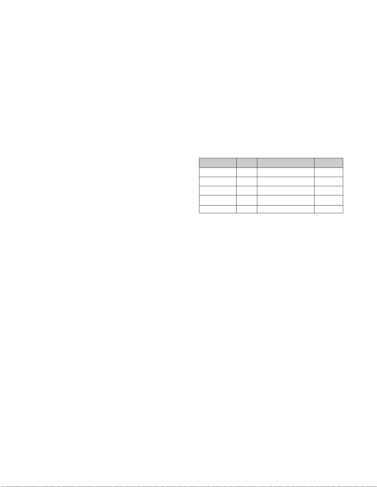
POWER CONSUMPTION
less than 120W
less than 8W
less than 8W
less than 3W
less than 1W
LED COLOR
GREEN
AMBER
AMBER
AMBER
-
MODE
MAX
STAND-BY
SUSPEND
DPM OFF
POWER SWITCH
OFF
VIDEO
Yes
No
No
No
-
SAFETY PRECAUTIONS
- 3 -
SAFETY-RELATED COMPONENT WARNING!
There are special components used in this color monitor
which are important for safety. These parts are marked
on the schematic diagram and the replacement
parts list. It is essential that these critical parts should be
replaced with the manufacturer's specified parts to prevent
X-radiation, shock, fire, or other hazards. Do not modify
the original design without obtaining written permission
from manufacturer or you will void the original parts and
labor guarantee.
CAUTION:
No modification of any circuit should be
attempted.
Service work should be performed only after
you are thoroughly familiar with all of the
following safety checks and servicing
guidelines.
SAFETY CHECK
Care should be taken while servicing this color monitor
because of the high voltage used in the deflection circuits.
These voltages are exposed in such areas as the
associated flyback and yoke circuits.
FIRE & SHOCK HAZARD
An isolation transformer must be inserted between the
color monitor and AC power line before servicing the
chassis.
• In servicing, attention must be paid to the original lead
dress specially in the high voltage circuit. If a short
circuit is found, replace all parts which have been
overheated as a result of the short circuit.
• All the protective devices must be reinstalled per the
original design.
• Soldering must be inspected for the cold solder joints,
frayed leads, damaged insulation, solder splashes, or
the sharp points. Be sure to remove all foreign
materials.
IMPLOSION PROTECTION
All used display tubes are equipped with an integral
implosion protection system, but care should be taken to
avoid damage and scratching during installation. Use only
same type display tubes.
X-RADIATION
The only potential source of X-radiation is the picture tube.
However, when the high voltage circuitry is operating
properly there is no possibility of an X-radiation problem.
The basic precaution which must be exercised is keep the
high voltage at the factory recommended level; the normal
high voltage is about 27kV. The following steps describe
how to measure the high voltage and how to prevent Xradiation.
Note : It is important to use an accurate high voltage
meter calibrated periodically.
• To measure the high voltage, use a high impedance
high voltage meter, connect (–) to chassis and (+) to
the CDT anode cap.
• Set the brightness control to maximum point at full
white pattern.
• Measure the high voltage. The high voltage meter
should be indicated at the factory recommended level.
• If the meter indication exceeds the maximum level,
immediate service is required to prevent the possibility
of premature component failure.
• To prevent X-radiation possibility, it is essential to use
the specified picture tube.
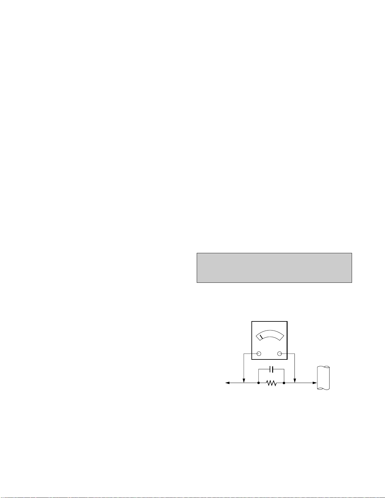
Leakage Current Hot Check Circuit
CAUTION:
Please use only a plastic screwdriver to protect yourself
from shock hazard during service operation.
1.5 Kohm/10W
To Instrument's
exposed
METALLIC PARTS
Good Earth Ground
such as WATER PIPE,
CONDUIT etc.
AC Volt-meter

- 4 -
SERVICING PRECAUTIONS
CAUTION: Before servicing receivers covered by this
service manual and its supplements and addenda, read
and follow the SAFETY PRECAUTIONS on page 3 of this
publication.
NOTE: If unforeseen circumstances create conflict
between the following servicing precautions and any of the
safety precautions on page 3 of this publication, always
follow the safety precautions. Remember: Safety First.
General Servicing Precautions
1. Always unplug the receiver AC power cord from the AC
power source before;
a. Removing or reinstalling any component, circuit
board module or any other receiver assembly.
b. Disconnecting or reconnecting any receiver electrical
plug or other electrical connection.
c. Connecting a test substitute in parallel with an
electrolytic capacitor in the receiver.
CAUTION: A wrong part substitution or incorrect
polarity installation of electrolytic capacitors may
result in an explosion hazard.
d. Discharging the picture tube anode.
2. Test high voltage only by measuring it with an
appropriate high voltage meter or other voltage
measuring device (DVM, FETVOM, etc) equipped with
a suitable high voltage probe.
Do not test high voltage by "drawing an arc".
3. Discharge the picture tube anode only by (a) first
connecting one end of an insulated clip lead to the
degaussing or kine aquadag grounding system shield
at the point where the picture tube socket ground lead
is connected, and then (b) touch the other end of the
insulated clip lead to the picture tube anode button,
using an insulating handle to avoid personal contact
with high voltage.
4. Do not spray chemicals on or near this receiver or any
of its assemblies.
5. Unless specified otherwise in this service manual,
clean electrical contacts only by applying the following
mixture to the contacts with a pipe cleaner, cottontipped stick or comparable non-abrasive applicator;
10% (by volume) Acetone and 90% (by volume)
isopropyl alcohol (90%-99% strength)
CAUTION: This is a flammable mixture.
Unless specified otherwise in this service manual,
lubrication of contacts in not required.
6. Do not defeat any plug/socket B+ voltage interlocks
with which receivers covered by this service manual
might be equipped.
7. Do not apply AC power to this instrument and/or any of
its electrical assemblies unless all solid-state device
heat sinks are correctly installed.
8. Always connect the test receiver ground lead to the
receiver chassis ground before connecting the test
receiver positive lead.
Always remove the test receiver ground lead last.
9. Use with this receiver only the test fixtures specified in
this service manual.
CAUTION: Do not connect the test fixture ground strap
to any heat sink in this receiver.
Electrostatically Sensitive (ES) Devices
Some semiconductor (solid-state) devices can be
damaged easily by static electricity. Such components
commonly are called Electrostatically Sensitive (ES)
Devices. Examples of typical ES devices are integrated
circuits and some field-effect transistors and
semiconductor "chip" components. The following
techniques should be used to help reduce the incidence of
component damage caused by static by static electricity.
1. Immediately before handling any semiconductor
component or semiconductor-equipped assembly, drain
off any electrostatic charge on your body by touching a
known earth ground. Alternatively, obtain and wear a
commercially available discharging wrist strap device,
which should be removed to prevent potential shock
reasons prior to applying power to the unit under test.
2. After removing an electrical assembly equipped with
ES devices, place the assembly on a conductive
surface such as aluminum foil, to prevent electrostatic
charge buildup or exposure of the assembly.
3. Use only a grounded-tip soldering iron to solder or
unsolder ES devices.
4. Use only an anti-static type solder removal device.
Some solder removal devices not classified as "antistatic" can generate electrical charges sufficient to
damage ES devices.
5. Do not use freon-propelled chemicals. These can
generate electrical charges sufficient to damage ES
devices.
6. Do not remove a replacement ES device from its
protective package until immediately before you are
ready to install it. (Most replacement ES devices are
packaged with leads electrically shorted together by
conductive foam, aluminum foil or comparable
conductive material).
7. Immediately before removing the protective material
from the leads of a replacement ES device, touch the
protective material to the chassis or circuit assembly
into which the device will be installed.
CAUTION: Be sure no power is applied to the chassis
or circuit, and observe all other safety precautions.
8. Minimize bodily motions when handling unpackaged
replacement ES devices. (Otherwise harmless motion
such as the brushing together of your clothes fabric or
the lifting of your foot from a carpeted floor can
generate static electricity sufficient to damage an ES
device.)

- 5 -
General Soldering Guidelines
1. Use a grounded-tip, low-wattage soldering iron and
appropriate tip size and shape that will maintain tip
temperature within the range or 500¡£F to 600¡£F.
2. Use an appropriate gauge of RMA resin-core solder
composed of 60 parts tin/40 parts lead.
3. Keep the soldering iron tip clean and well tinned.
4. Thoroughly clean the surfaces to be soldered. Use a
mall wire-bristle (0.5 inch, or 1.25cm) brush with a
metal handle.
Do not use freon-propelled spray-on cleaners.
5. Use the following unsoldering technique
a. Allow the soldering iron tip to reach normal
temperature.
(500¡£F to 600¡£F)
b. Heat the component lead until the solder melts.
c. Quickly draw the melted solder with an anti-static,
suction-type solder removal device or with solder
braid.
CAUTION: Work quickly to avoid overheating the
circuitboard printed foil.
6. Use the following soldering technique.
a. Allow the soldering iron tip to reach a normal
temperature (500¡£F to 600¡£F)
b. First, hold the soldering iron tip and solder the strand
against the component lead until the solder melts.
c. Quickly move the soldering iron tip to the junction of
the component lead and the printed circuit foil, and
hold it there only until the solder flows onto and
around both the component lead and the foil.
CAUTION: Work quickly to avoid overheating the
circuit board printed foil.
d. Closely inspect the solder area and remove any
excess or splashed solder with a small wire-bristle
brush.
IC Remove/Replacement
Some chassis circuit boards have slotted holes (oblong)
through which the IC leads are inserted and then bent flat
against the circuit foil. When holes are the slotted type,
the following technique should be used to remove and
replace the IC. When working with boards using the
familiar round hole, use the standard technique as
outlined in paragraphs 5 and 6 above.
Removal
1. Desolder and straighten each IC lead in one operation
by gently prying up on the lead with the soldering iron
tip as the solder melts.
2. Draw away the melted solder with an anti-static
suction-type solder removal device (or with solder
braid) before removing the IC.
Replacement
1. Carefully insert the replacement IC in the circuit board.
2. Carefully bend each IC lead against the circuit foil pad
and solder it.
3. Clean the soldered areas with a small wire-bristle
brush. (It is not necessary to reapply acrylic coating to
the areas).
"Small-Signal" Discrete Transistor
Removal/Replacement
1. Remove the defective transistor by clipping its leads as
close as possible to the component body.
2. Bend into a "U" shape the end of each of three leads
remaining on the circuit board.
3. Bend into a "U" shape the replacement transistor leads.
4. Connect the replacement transistor leads to the
corresponding leads extending from the circuit board
and crimp the "U" with long nose pliers to insure metal
to metal contact then solder each connection.
Power Output, Transistor Device
Removal/Replacement
1. Heat and remove all solder from around the transistor
leads.
2. Remove the heat sink mounting screw (if so equipped).
3. Carefully remove the transistor from the heat sink of the
circuit board.
4. Insert new transistor in the circuit board.
5. Solder each transistor lead, and clip off excess lead.
6. Replace heat sink.
Diode Removal/Replacement
1. Remove defective diode by clipping its leads as close
as possible to diode body.
2. Bend the two remaining leads perpendicular y to the
circuit board.
3. Observing diode polarity, wrap each lead of the new
diode around the corresponding lead on the circuit
board.
4. Securely crimp each connection and solder it.
5. Inspect (on the circuit board copper side) the solder
joints of the two "original" leads. If they are not shiny,
reheat them and if necessary, apply additional solder.
Fuse and Conventional Resistor
Removal/Replacement
1. Clip each fuse or resistor lead at top of the circuit board
hollow stake.
2. Securely crimp the leads of replacement component
around notch at stake top.
3. Solder the connections.
CAUTION: Maintain original spacing between the
replaced component and adjacent components and the
circuit board to prevent excessive component
temperatures.

- 6 -
Circuit Board Foil Repair
Excessive heat applied to the copper foil of any printed
circuit board will weaken the adhesive that bonds the foil
to the circuit board causing the foil to separate from or
"lift-off" the board. The following guidelines and
procedures should be followed whenever this condition is
encountered.
At IC Connections
To repair a defective copper pattern at IC connections use
the following procedure to install a jumper wire on the
copper pattern side of the circuit board. (Use this
technique only on IC connections).
1. Carefully remove the damaged copper pattern with a
sharp knife. (Remove only as much copper as
absolutely necessary).
2. carefully scratch away the solder resist and acrylic
coating (if used) from the end of the remaining copper
pattern.
3. Bend a small "U" in one end of a small gauge jumper
wire and carefully crimp it around the IC pin. Solder the
IC connection.
4. Route the jumper wire along the path of the out-away
copper pattern and let it overlap the previously scraped
end of the good copper pattern. Solder the overlapped
area and clip off any excess jumper wire.
At Other Connections
Use the following technique to repair the defective copper
pattern at connections other than IC Pins. This technique
involves the installation of a jumper wire on the
component side of the circuit board.
1. Remove the defective copper pattern with a sharp
knife.
Remove at least 1/4 inch of copper, to ensure that a
hazardous condition will not exist if the jumper wire
opens.
2. Trace along the copper pattern from both sides of the
pattern break and locate the nearest component that is
directly connected to the affected copper pattern.
3. Connect insulated 20-gauge jumper wire from the lead
of the nearest component on one side of the pattern
break to the lead of the nearest component on the
other side.
Carefully crimp and solder the connections.
CAUTION: Be sure the insulated jumper wire is
dressed so the it does not touch components or sharp
edges.
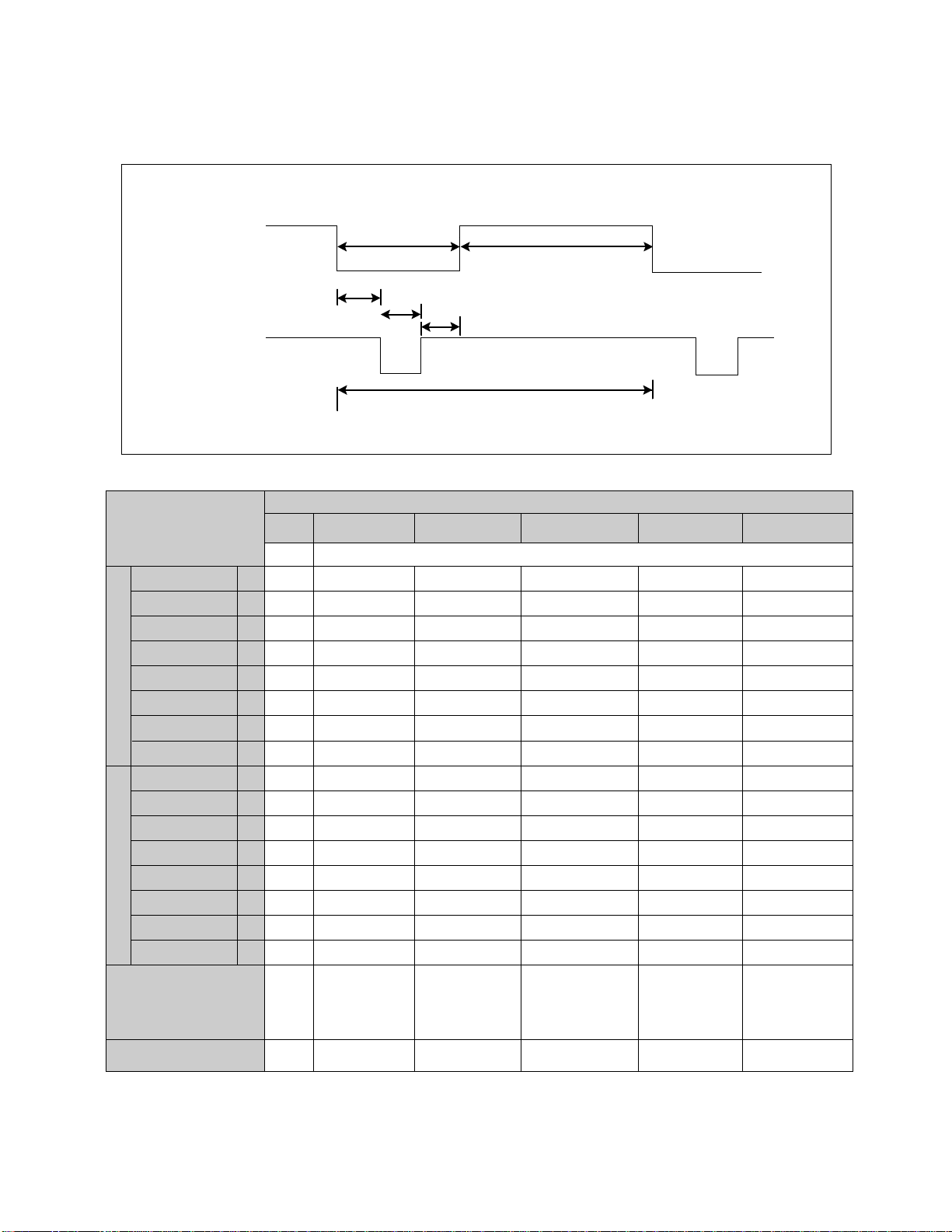
TIMING CHART
- 7 -
VIDEO
kHz
µs
µs
µs
µs
µs
µs
Hz
ms
ms
ms
ms
ms
ms
MODE 1
–
43.269
23.112
17.778
5.334
1.556
1.556
2.222
–
85.008
11.763
11.093
0.670
0.023
0.069
0.578
640
X
480
85Hz
Yes
MODE 2
+
53.674
18.631
14.222
4.409
0.569
1.138
2.702
+
85.061
11.756
11.178
0.578
0.019
0.056
0.503
800
X
600
85Hz
Yes
MODE 3
+
68.677
14.561
10.836
3.725
0.508
1.016
2.201
+
84.997
11.765
11.183
0.582
0.015
0.044
0.523
1024
X
768
85Hz
Yes
MODE 4
+
91.146
10.971
8.127
2.844
0.406
1.016
1.422
+
85.024
11.762
11.235
0.527
0.011
0.033
0.483
1280
X
1024
85Hz
Yes
MODE 5
+
93.750
10.666
7.901
2.765
0.316
0.948
1.501
+
75.000
13.333
12.800
0.533
0.011
0.032
0.490
1600
X
1200
75Hz
MARK
A
B
C
D
E
F
A
B
C
D
E
F
MODE
FACTORY PRESET MODE
Resolution
Recall
H
O
R
I
Z
O
N
T
A
L
V
E
R
T
I
C
A
L
Sync Polarity
Frequency
Total Period
Video Active Time
Blanking Time
Front Porch
Sync Duration
Back Porch
Sync Polarity
Frequency
Total Period
Video Active Time
Blanking Time
Front Porch
Sync Duration
Back Porch
VESA
BC
SYNC
D
F
E
A
DISASSEMBLY
- 8 -
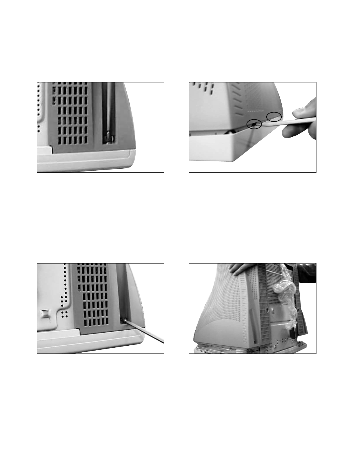
1. Carefully place the monitor on a soft cushion
and stand it upright with the cabinet facing
downward.
2. Remove the two screws from the back cover.
4. Separate the back cover from the latch at the
bottom of the cabinet using the jig as shown in
the figure.
(Insert the jig into the latch and lift slightly.)
3. Separate the back cover from the latch on top
of the cabinet using a screwdriver as shown in
the figure.
(Insert the screwdriver and gently press the
latch.)
5. Lift up the back cover to separate from cabinet
assembly.
1. Preparation for Service Adjustment
GENERAL INFORMATION
All adjustment are thoroughly checked and corrected
when the monitor leaves the factory, but sometimes
several adjustments may be required.
Adjustment should be following procedure and after
warming up for a minimum of 30 minutes.
• Alignment appliances and tools.
- IBM compatible PC.
- Programmable Signal Generator.
(eg. VG-819 made by Astrodesign Co.)
- EPROM or EEPROM with saved each mode data.
- Alignment Adaptor and Software.
- Digital Voltmeter.
- White Balance Meter.
- Luminance Meter.
- High-voltage Meter.
AUTOMATIC AND MANUAL DEGAUSSING
The degaussing coil is mounted around the CDT so that
automatic degaussing when turn on the monitor. But a
monitor is moved or faced in a different direction, become
poor color purity cause of CDT magnetized, then press
DEGAUSSING on the OSD menu.
ADJUSTMENT PROCEDURE & METHOD
- Install the cable for adjustment such as Figure 1and run
the alignment program on the DOS for IBM
compatible PC.
- Set external Brightness and Contrast volume to max
position.
1. Adjustment for B+ Voltage.
1) Display cross hatch pattern at Mode 4.
2) Adjust C905 (+) voltage to 190V ±0.5V with VR901.
2. Adjustment for High-Voltage.
1) Display cross hatch pattern at Mode 4.
2) Adjust CDT Anode voltage to 27kV ± 0.2kV with
VR801.
3. Adjustment for Horizontal Raster Center.
1) Display cross hatch pattern at Mode 4.
2) Adjust the Back Raster should be center of the
screen with SW801.
2. Adjustment by Service Hot key
How to enter SVC HOT KEY
1. Press Menu and OSD window will appear.
2. While OSD window is displayed,
is seen on the
left bottom of OSD window.
3. Press
+ simultaneously and the screen will
immediately refresh.
4. Press Menu and make sure that
is changed to
1 2.
5. Follow the menu on the left of OSD window to find 12
and OSD will change as shown in the figure.
6. Select Degauss in the above figure and then press
Select and
to change the screen as shown in the
figure. (Back Raster for Pattern)
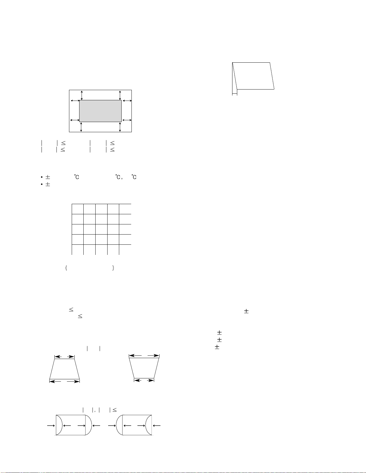
FOS SPEC
1. Size
H : 350
4mm
V : 262
4mm
Scanning frequency : All Mode (Mode 1~5)
Display image : Crosshatch pattern
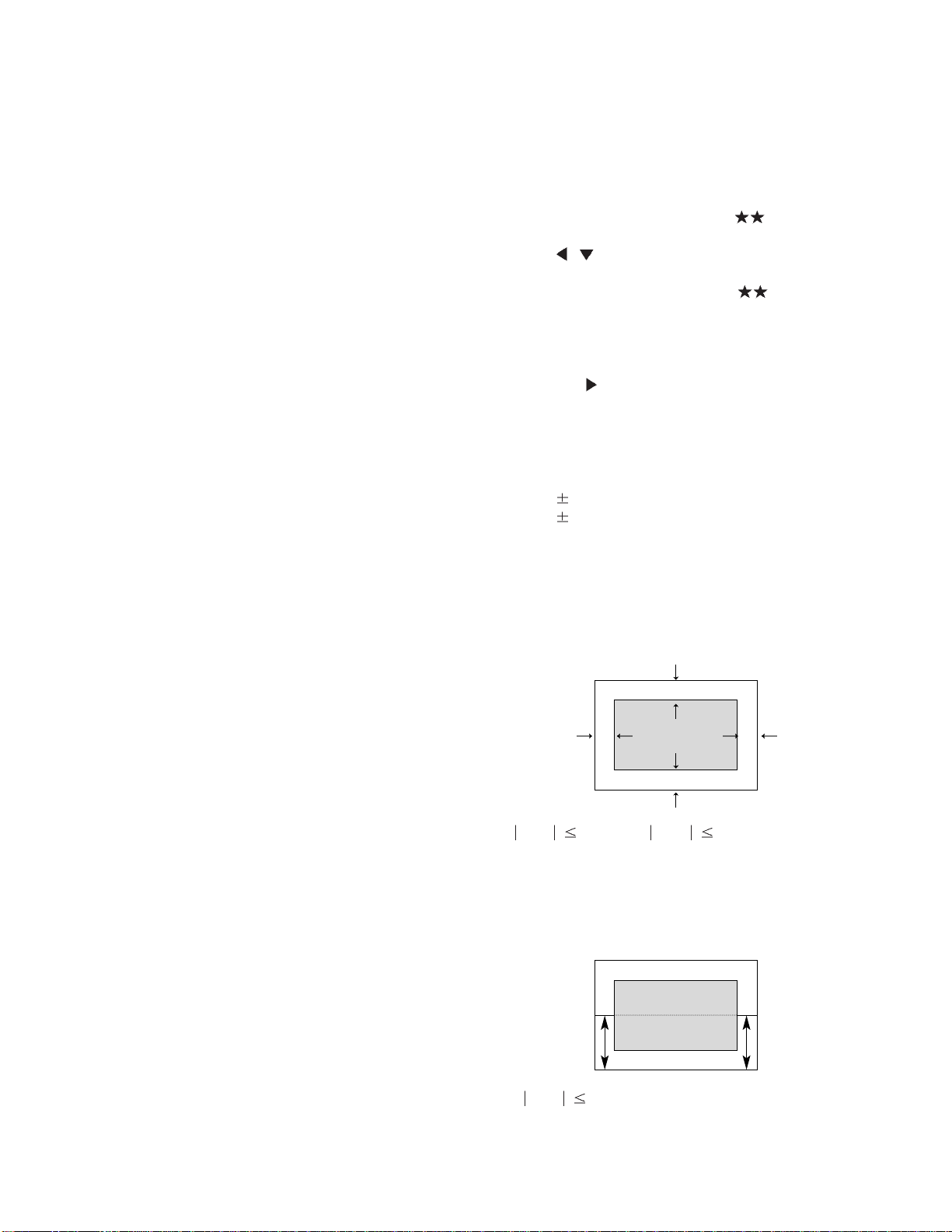
2. Centering
Scanning frequency : All Mode (Mode 1~5)
Display image : Crosshatch pattern
Horizontal : 10 Row
Vertical : 8 Row
H :
L-R 4mm, V : U-D 4mm
3. Tilt
Scanning frequency : All Mode (Mode 1~5)
Display image : Crosshatch pattern
Horizontal : 10 Row
Vertical : 8 Row
Tilt :
E-F 2.0mm
- 9 -
ADJUSTMENT
U
D
L
R
EF
- 10 -
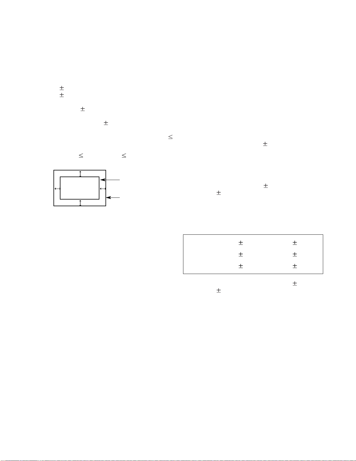
4. Distortion
Scanning frequency : All Mode (Mode 1~5)
Display image : Crosshatch pattern
Horizontal : 10 Row
Vertical : 8 Row
A-B 2.5mm, C-D 2.5mm
E-F 2.0mm, G-H 2.0mm
5. Displa Size drift
4mm : 25 Standard, 10 35
0.5mm : 180V ~ 264V
6. Linearity
Formula :
(Max - Min) / Max x 100(%)
Criteria : H - 10% Max. (Upper 40kHz)
12% Max. (Less 40kHz)
V - 8% Max.
7. Regulation
Luminance
1mm
Dynamic(lode) 1mm
Scanning frequency : All Mode (Mode 1~5)
8. Trapezoid
9. Pin Balance
10.Parallelogram
11. Adjustment of white balance (Adjustment of
chromaticity diagram)
*(Adjustment of white balance must be made after
entering Hot Key Mode and DEGAUSS.)
CONDITIONS
Signal: 91 kHz / 85 Hz
Display image: Back raster (Color 0,0)
Contrast: Maximum
Brightness: Maximum
Color temperature: 9300K
11-1. Adjustment of cut off (Adjustment of back raster)
11-1(a). Before adjustment, press Menu and Degauss
to remove.
=> Enter hot key mode.
Adjust Brightness and Contrast to Max in OSD
window.
(1)Adjust cut off (back raster) first. Enter DEGAUSS in
the Menu and modify the following data.
Modify RCUT to Min ( 1 ) ,
Modify GCUT To Min ( 1 ) ,
Adjust to BCUT Data = 70 (46 (h)) ,
Adjust to SBRT Data = 90 ( 5A (h)).
(2)Turn FBT screen volume on "CRT COLOR
ANALYZER CA-100" equipment to adjust
Brightness to 0.15
0.05FL.
(3)Adjust RCUT, GCUT, and SBRT to set chromaticity
diagram at :
x: 0.283
0.003
y: 0.298 0.003
Y: 0.40
0.05FL
* If color values would not be matched desirable values,
repeat sequence 1 and 2 after readjusting “GREEN
CUTOFF” control a little different.
U
D
D
U
U-D
< 4mm
L1 R1
2.0mm
L1
R1 L1
R1
Y1
Y2
Y3
Y4
X1 X2 X3 X4
4mm
A B
DC
EG
FH
11-2. Adjustment of White Balance
After finishing adjustment of cut off (back raster),
approve "Color(15.0) Full white pattern".
Adjust to BDRV Data = 94.
Adjust RDRV and GDRV to set chromaticity diagram at :
x: 0.283 0.003
y: 0.298 0.003
Approve "Window pattern (70x70mm)" to adjust
S-CON to Y : 40
1FL.
Approve "Color (15.0) Full white pattern" again and
adjust ABL Data to Y : 30 1FL
Adjust the horizontal position and vertical position to
4.0 mm of the center point of the screen.
*
SIZE adjustment should be made in ALL Mode.
12. Focus Adjustment
CONDITIONS
Scanning frequency : All Mode (Mode 1~5)
Display image: “H” character pattern
Brightness: Cut off point
Contrast: Maximum
PROCEDURE
1. Adjust the Focus VR on the FBT to display the
sharpest image possible.
2. Use Locktite to seal the Focus VR in position.
14. Color Purity Adjustment
Color purity is the absence of undesired color.
Conspicuous mislanding (unexpected color in a uniform
field) within the display area shall not be visible at a
distance of 50 cm from the CRT surface.
CONDITIONS
Orientation: Monitor facing east
Scanning Frequency: 1208 x 1024@85Hz(91kHz/85Hz)
Display image: White flat field
Luminance: Cut off point at the center of the
display area
Note: Color purity adjustments should only be
attempted by qualified personnel.
PROCEDURE
For trained and experienced service technicians only.
Use the following procedure to correct minor color
purity problems:
1. Make sure the display is not affected by external
magnetic fields.
2. Very carefully break the glue seal between the 2-pole
purity convergence magnets (PCM), the band and
the spacer.
3. Make sure the spacing between the PCM assembly
and the CRT stem is 29 mm
1 mm.
4. Display a green pattern over the entire display area.
5. Adjust the purity magnet rings on the PCM assembly
to display a pure green pattern.
(Optimum setting: x = 0.295
0.015,
y = 0.594 0.015)
6. Repeat steps 4 and 5 using a red pattern and then
again, using a blue pattern.
Table 4-6. Color Purity Tolerances
(For 9300K color adjustment: x = 0.283 0.02,
y = 0.298
0.02)
7. When you have the PCMs properly adjusted,
carefully glue them together to prevent their
movement during shipping.
- 11 -
U
DISPLAY AREA
EDGE OF BEZEL
D
LR
|L-R| 4.0 mm. |U-D| 4.0 mm.
Red: x=0.620
0.015 y=0.334 0.015
Green: x=0.620
0.015 y=0.334 0.015
Blue: x=0.620 0.015 y=0.334 0.015

- 12 -
3. Adjustment Using Service software Program
(Adjustment Program)
1. Adjustment for Factory Mode (Preset Mode).
1) Display cross hatch pattern at Mode All.
2) Run alignment program for F900BJ on the IBM
compatible PC.
3) EEPROM → ALL CLEAR → Y(Yes) command.
<Caution> Do not run this procedure unless the
EEPROM is changed. All data in EEPROM (mode
data and color data) will be erased.
4) COMMAND → PRESET START → Y(Yes)
command.
5) DIST. ADJ. → FOS. ADJ command.
6) Adjust H-POSITION as arrow keys to center of the
screen.
7) Adjust H-SIZE as arrow keys to 350 ± 2mm.
8) Adjust V-POSITION as arrow keys to center of the
screen.
9) Adjust V-SIZE as arrow keys to 262 ± 2mm.
10) Adjust TRAPEZOID as arrow keys to be the best
condition.
11) Adjust SIDE PINCUSHON as arrow keys to be the
best condition.
12) Adjust TILT as arrow keys to be the best condition.
13) Display cross hatch pattern at Mode 4.
14) DIST. ADJ. → BALANCE DATA command.
15) Adjust balance of Pin-Balance as arrow keys to be
the best condition.
16) Adjust parallelogram as arrow keys to be the best
condition.
17) Save of the Mode.
18) Save of the System.
19) Display from Mode 4 and repeat above from number
6) to 16).
20) COMMAND → PRESET EXIT → Y (Yes) command.
2. Adjustment for White Balance and Luminance.
1) Set the White Balance Meter.
2) Press the DEGAUSSING on the OSD menu for
demagnetization of the CDT.
3) Display color 0,0 pattern at Mode 4.
4) COMMAND → PRESET START → Y(Yes)
command.
5) Set Bightness and Contrast to max position.
6) COLOR ADJ. → LUMINANCE command of the
alignment program.
7) COLOR ADJ. → BIAS ADJ. command of the
alignment program.
8) Check whether blue color or not at R-BIAS and GBIAS to min position, Sub-Brightness to 90
(5A(h))position, B-Bias to 70(46(h))position. If it's not
blue color, the monitor must repair.
9) Adjust Screen control on the FBT to 0.15 ± 0.05FL
of the raster luminance.
10) Adjust R-BIAS and G-BIAS command to x=0.283 ±
0.006 and y=0.298 ± 0.006 on the White Balance
Meter with PC arrow keys.
11)Display color 15,0 Full White(70x70mm) at mode 4.
12)DRIVE ADJ command.
13)Set B-DRIVE to 94(5E(h)) at DRIVE of the alignment
program.
14) Adjust R-DRIVE and G-DRIVE command to white
balance x=0.283 ± 0.003 and y=0.298 ± 0.003 on
the White Balance Meter with PC arrow keys.
15)Adjust SUB-CONTRAST command to 40±1FL of the
raster luminance.
15)Display color 15,0 full white patten at Mode 4.
16)COLOR ADJ. → LUMINANCE → ABL command.
17) Adjust ABL to 30 ± 1FL of the luminance.
18) Exit from the program.
- 13 -
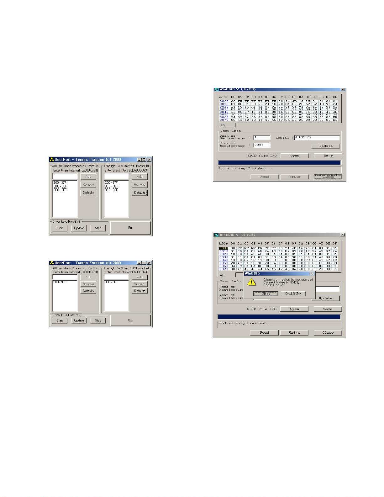
Windows EDID V1.0 User Manual
Operating System: MS Windows 98, 2000, XP
Port Setup: Windows 98 => Don’t need setup
Windows 2000, XP => Need to Port Setup.
This program is available to LCD Monitor only.
1. Port Setup
a) Copy “UserPort.sys” file to
“c:\WINNT\system32\drivers” folder
b) Run Userport.exe
c) Remove all default number
d) Add 300-3FF
e) Click Start button.
f) Click Exit button.
2. EDID Read & Write
1) Run WinEDID.exe
2) Edit Week of Manufacture, Year of Manufacture,
Serial Number
a) Input User Info Data
b) Click “Update” button
c) Click “ Write” button
- Adjustment and EDID Data Down in GCSC
- 14 -
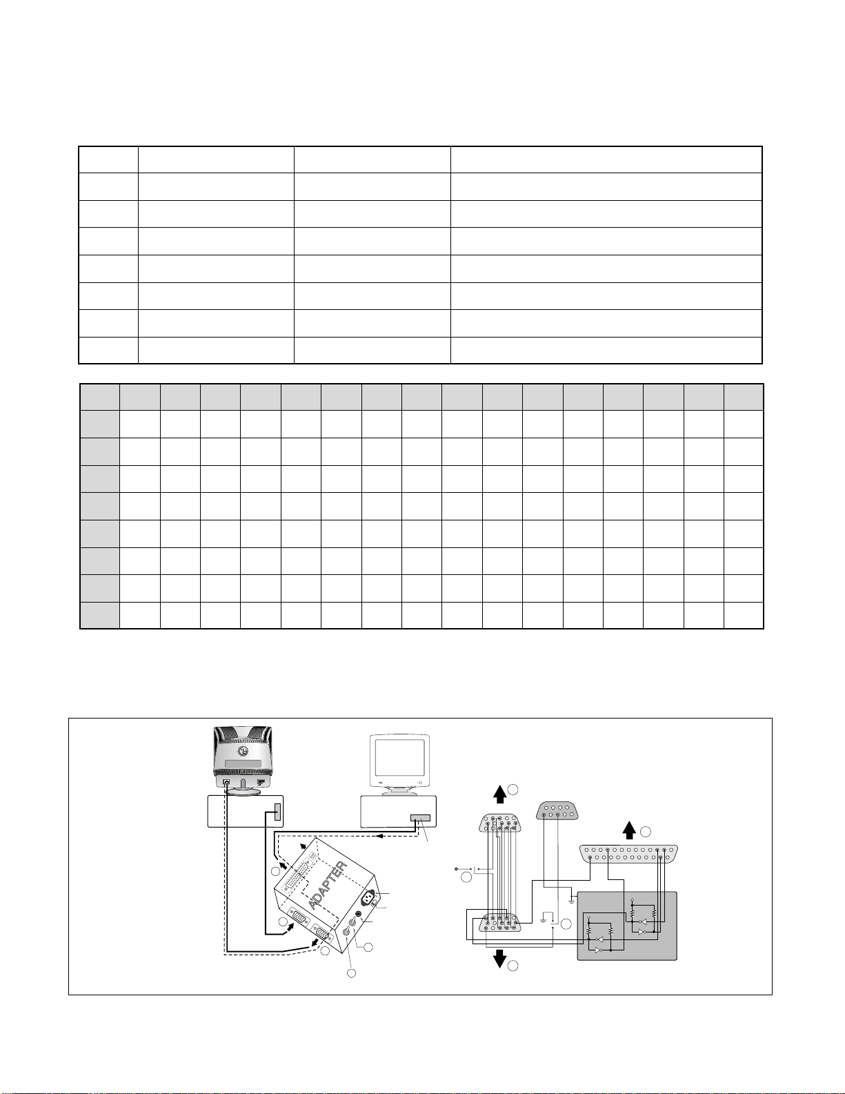
Figure 1. Cable Connection
220
IBM
Compatible PC
PARALLEL PORT
Power inlet (required)
Power LED
ST Switch
Power Select Switch
(110V/220V)
Control Line
Not used
RS232C
PARALLEL
V-SYNC
POWER
ST
VGS
MONITOR
E
V-Sync On/Off Switch
(Switch must be ON.)
F
A
B
C
E
F
A
B
C
15
10
5
5
69
1
1
1
14
13
25
6
5V
5V
5V
4.7K
4.7K
4.7K
74LS06
74LS06
OFF ON
OFF
ON
11
VIDEO
SIGNAL
GENERATOR
EDID DATA EDIT
- Changeable Data
* : Serial No : Controlled / Data : 01
** : Week : Not Controlled / Data : 00
*** : Year : Controlled
No Item Content Hexadecimal
1 Manufacturer ID GSM 1E6D
2 Product ID 19093 4A95
3 Year 2004 0E
4 Version 1 01
5 Revision 3 03
6 Model name F920BJ 7 Special
0x00 0x01 0x02 0x03 0x04 0x05 0x06 0x07 0x08 0x09 0x0A 0x0B 0x0C 0x0D 0x0E 0x0F
0x00 00 FF FF FF FF FF FF 00 1E 6D 95 4A 01
* 00* 00* 00*
0x01 01** 0E*** 01 03 7C 24 1B BF E8 9A D9 A1 54 4B 99 24
0x02 12 48 4C FF FF 80 31 59 45 59 61 59 81 80 A9 40
0x03 E1 40 A9 4A A9 4F 86 3D 00 C0 51 00 30 40 40 A0
0x04 13 00 5E 06 11 00 00 1E 00 00 00 FD 00 32 A0 1E
0x05 62 1B 00 0A 20 20 20 20 20 20 00 00 00 FC 00 46
0x06 39 32 30 42 0A 20 20 20 20 20 20 20 00 00 00 FC
0x07 00 0A 20 20 20 20 20 20 20 20 20 20 20 20 00 2D
 Loading...