

Page 1

SERVICE MANUAL
SERVICE MANUAL
CAUTION
BEFORE SERVICING THE UNIT, READ THE “SAFETY PRECAUTIONS”
IN THIS MANUAL.
Internal Use Only
Website http://biz.lgservice.com
JULY, 2015
MODEL: DP547
MODEL: DP547
DVD Player
P/NO : AFN76412152
Page 2

CONTENTS
SECTION 1 ........ SUMMARY
SECTION 2 ........ CABINET & MAIN CHASSIS
SECTION 3 ........ ELECTRICAL
SECTION 4 ........ REPLACEMENT PARTS LIST
1-1
Page 3

SECTION 1
SUMMARY
CONTENTS
PRODUCT SAFETY SERVICING GUIDELINES FOR DVD PRODUCTS .................................................. 1-3
SERVICING PRECAUTIONS .......................................................................................................................... 1-4
• GENERAL SERVICING PRECAUTIONS
• INSULATION CHECKING PRODEDURE
• ELECTROSTATICALLY SENSITIVE (ES) DEVICES
THE PROCESS OF USB DOWNLOAD ......................................................................................................... 1-5
SPECIFICATIONS ............................................................................................................................................ 1-8
1-2
Page 4
PRODUCT SAFETY SERVICING GUIDELINES FOR DVD PRODUCTS
IMPORTANT SAFETY NOTICE
This manual was prepared for use only by properly trained audio-video service
technicians.
When servicing this product, under no circumstances should the original design be
modified or altered without permission from LG Corporation. All components should
be replaced only with types identical to those in the original circuit and their physical
location, wiring and lead dress must conform to original layout upon completion of
repairs.
Special components are also used to prevent x-radiation, shock and fire hazard.
These components are indicated by the letter “x” included in their component designators and are required to maintain safe performance. No deviations are allowed
without prior approval by LG Corporation.
Circuit diagrams may occasionally differ from the actual circuit used. This way,
implementation of the latest safety and performance improvement changes into the
set are not delayed until the new service literature is printed.
CAUTION: Do not attempt to modify this product in any way. Never perform cus-
tomized installations without manufacturer’s approval. Unauthorized modifications
will not only void the warranty, but may lead to property damage or user injury.
Service work should be performed only after you are thoroughly familiar with these
safety checks and servicing guidelines.
GRAPHIC SYMBOLS
The exclamation point within an equilateral triangle is intended to
alert the service personnel to important safety information in the
service literature.
The lightning flash with arrowhead symbol within an equilateral
triangle is intended to alert the service personnel to the presence of
noninsulated “dangerous voltage” that may be of sufficient magnitude
to constitute a risk of electric shock.
The pictorial representation of a fuse and its rating within an equilateral triangle is intended to convey to the service personnel the
following fuse replacement caution notice:
CAUTION: FOR CONTINUED PROTECTION AGAINST RISK
OF FIRE, REPLACE ALL FUSES WITH THE SAME TYPE AND
RATING AS MARKED NEAR EACH FUSE.
SERVICE INFORMATION
While servicing, use an isolation transformer for protection from AC line shock. After
the original service problem has been corrected, make a check of the following:
FIRE AND SHOCK HAZARD
1. Be sure that all components are positioned to avoid a possibility of adjacent
component shorts. This is especially important on items trans-ported to and from
the repair shop.
2. Verify that all protective devices such as insulators, barriers, covers, shields,
strain reliefs, power supply cords, and other hardware have been reinstalled per
the original design. Be sure that the safety purpose of the polarized line plug has
not been defeated.
3. Soldering must be inspected to discover possible cold solder joints, solder
splashes, or sharp solder points. Be certain to remove all loose foreign particles.
4. Check for physical evidence of damage or deterioration to parts and components, for frayed leads or damaged insulation (including the AC cord), and
replace if necessary.
5. No lead or component should touch a high current device or a resistor rated at 1
watt or more. Lead tension around protruding metal surfaces must be avoided.
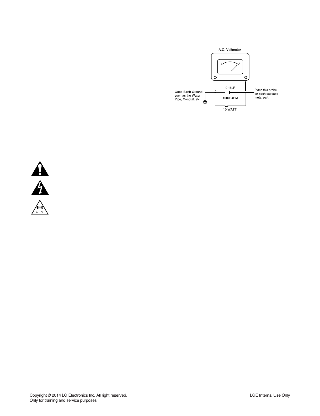
6. After reassembly of the set, always perform an AC leakage test on all exposed
metallic parts of the cabinet (the channel selector knobs, antenna terminals,
handle and screws) to be sure that set is safe to operate without danger of
electrical shock. DO NOT USE A LINE ISOLATION TRANSFORMER DURING
THIS TEST. Use an AC voltmeter having 5000 ohms per volt or more sensitivity
in the following manner: Connect a 1500 ohm, 10 watt resistor, paralleled by a
.15 mfd 150V AC type capacitor between a known good earth ground water pipe,
conduit, etc.) and the exposed metallic parts, one at a time. Measure the AC voltage across the combination of 1500 ohm resistor and .15 mfd capacitor. Reverse
the AC plug by using a non-polarized adaptor and repeat AC voltage measurements for each exposed metallic part. Voltage measured must not exceed 0.75
volts RMS. This corresponds to 0.5 milliamp AC. Any value exceeding this limit
constitutes a potential shock hazard and must be corrected immediately.
TIPS ON PROPER INSTALLATION
1. Never install any receiver in a closed-in recess, cubbyhole, or closely fitting shelf
space over, or close to, a heat duct, or in the path of heated air flow.
2. Avoid conditions of high humidity such as: outdoor patio installations where dew
is a factor, near steam radiators where steam leakage is a factor, etc.
3. Avoid placement where draperies may obstruct venting. The customer should
also avoid the use of decorative scarves or other coverings that might obstruct
ventilation.
4. Wall- and shelf-mounted installations using a commercial mounting kit must
follow the factory-approved mounting instructions. A product mounted to a shelf
or platform must retain its original feet (or the equivalent thickness in spacers) to
provide adequate air flow across the bottom. Bolts or screws used for fasteners
must not touch any parts or wiring. Perform leakage tests on customized installations.
5. Caution customers against mounting a product on a sloping shelf or in a tilted
position, unless the receiver is properly secured.
6. A product on a roll-about cart should be stable in its mounting to the cart.
Caution the customer on the hazards of trying to roll a cart with small casters
across thresholds or deep pile carpets.
7. Caution customers against using extension cords. Explain that a forest of extensions, sprouting from a single outlet, can lead to disastrous consequences to
home and family.
1-3
Page 5

SERVICING PRECAUTIONS
CAUTION: Before servicing the DVD covered by this service
data and its supplements and addends, read and follow the
SAFETY PRECAUTIONS. NOTE: if unforeseen circumstances create conflict between the following servicing precautions
and any of the safety precautions in this publication, always
follow the safety precautions.
Remember Safety First :
General Servicing Precautions
1. Always unplug the DVD AC power cord from the AC power
source before:
(1) Removing or reinstalling any component, circuit board,
module, or any other assembly.
(2) Disconnecting or reconnecting any internal electrical
plug or other electrical connection.
(3) Connecting a test substitute in parallel with an electro-
lytic capacitor.
Caution: A wrong part substitution or incorrect polarity
installation of electrolytic capacitors may result in an
explosion hazard.
2. Do not spray chemicals on or near this DVD or any of its
assemblies.
3. Unless specified otherwise in this service data, clean electrical contacts by applying an appropriate contact cleaning
solution to the contacts with a pipe cleaner, cotton-tipped
swab, or comparable soft applicator.
Unless specified otherwise in this service data, lubrication
of contacts is not required.
4. Do not defeat any plug/socket B+ voltage interlocks with
which instruments covered by this service manual might be
equipped.
5. Do not apply AC power to this DVD and / or any of its electrical assemblies unless all solid state device heat sinks are
correctly installed.
6. Always connect the test instrument ground lead to an
appropriate ground before connecting the test instrument
positive lead. Always remove the test instrument ground
lead last.
Insulation Checking Procedure
Disconnect the attachment plug from the AC outlet and
turn the power on. Connect an insulation resistance meter
(500V)
to the blades of the attachment plug. The insulation resistance
between each blade of the attachment plug and accessible
conductive parts (Note 1) should be more than 1Mohm.
Note 1: Accessible Conductive Parts include Metal panels,
Input terminals, Earphone jacks,etc.
Electrostatically Sensitive (ES) Devices
Some semiconductor (solid state) devices can be damaged
easily by static electricity. Such components commonly are
called Electrostatically Sensitive (ES) Devices. Examples
of typical ES devices are integrated circuits and some field
effect transistors and semiconductor chip components.
The following techniques should be used to help reduce the
incidence of component damage caused by static electricity.
1. Immediately before handling any semiconductor component or semiconductor-equipped assembly, drain off any
electrostatic charge on your body by touching a known
earth ground. Alternatively, obtain and wear a commercially available discharging wrist strap device, which should
be removed for potential shock reasons prior to applying
power to the unit under test.
2. After removing an electrical assembly equipped with ES
devices, place the assembly on a conductive surface such
as aluminum foil, to prevent electrostatic charge buildup or
exposure of the assembly.
3. Use only a grounded-tip soldering iron to solder or unsolder
ES devices.
4. Use only an anti-static solder removal device. Some solder
removal devices not classified as “anti-static” can generate
electrical charges sufficient to damage ES devices.
5. Do not use freon-propelled chemicals. These can generate
an electrical charge sufficient to damage ES devices.
6. Do not remove a replacement ES device from its protective
package until immediately before you are ready to install
it. (Most replacement ES devices are packaged with leads
electrically shorted together by conductive foam, aluminum
foil, or comparable conductive material).
7. Immediately before removing the protective material from
the leads of a replacement ES device, touch the protective
material to the chassis or circuit assembly into which the
device will be installed.
Caution: Be sure no power is applied to the chassis or
circuit, and observe all other safety precautions.
8. Minimize bodily motions when handling unpackaged
replacement ES devices. (Normally harmless motion such
as the brushing together of your clothes fabric or the lifting
of your foot from a carpeted floor can generate static electricity sufficient to damage an ES device.)
1-4
Page 6
THE PROCESS OF USB DOWNLOAD
Please follow the below process to download a program with disc
1. Turn on the DVD-player.
Note: Be sure that there is no disc in DVD-player.
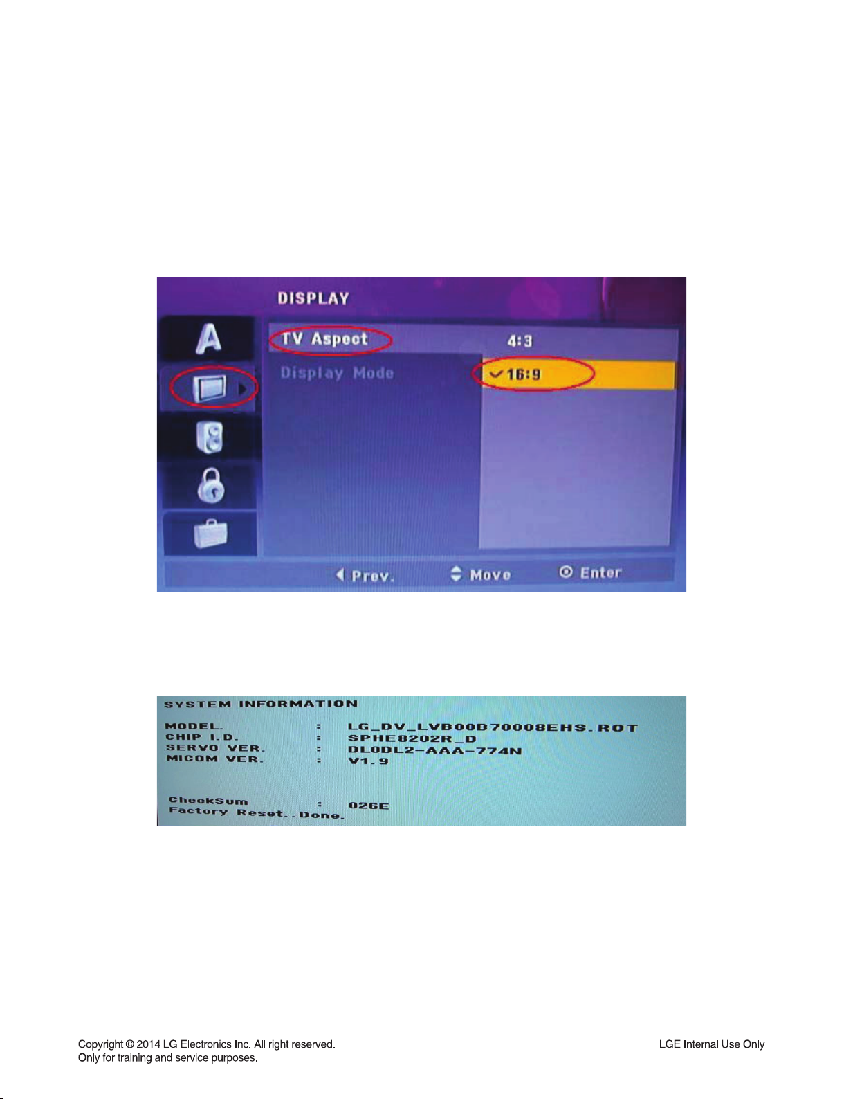
2. Press “SETUP” button on Remote control.
3. Choose a “DISPLAY” menu by using the cursor button and then choose a “TV Aspect” menu.
And choose “16:9” menu.
4. Press the 1 --> 3 --> 9 --> 7 --> 1 --> 3 --> 9(Numerical button) --> Enter key on remote control
to confi rm the system information.
5. Remember or write the model.
6. Change the program fi le name of new version to the model.
Example:
New ver. program fi le: LG_DV_LVB00B70000EHS_V1.9.ROT
Model: LG_DV_LVB00B70008EHS.ROT
Change New ver. program fi le like this LG_DV_LVB00B70008EHS.ROT
If you don’t change the fi le name like that,disc download isn’t be worked.
7. Copy the changed fi le to a USB memory stick or burn it to CD-R/RW.
1-5
Page 7
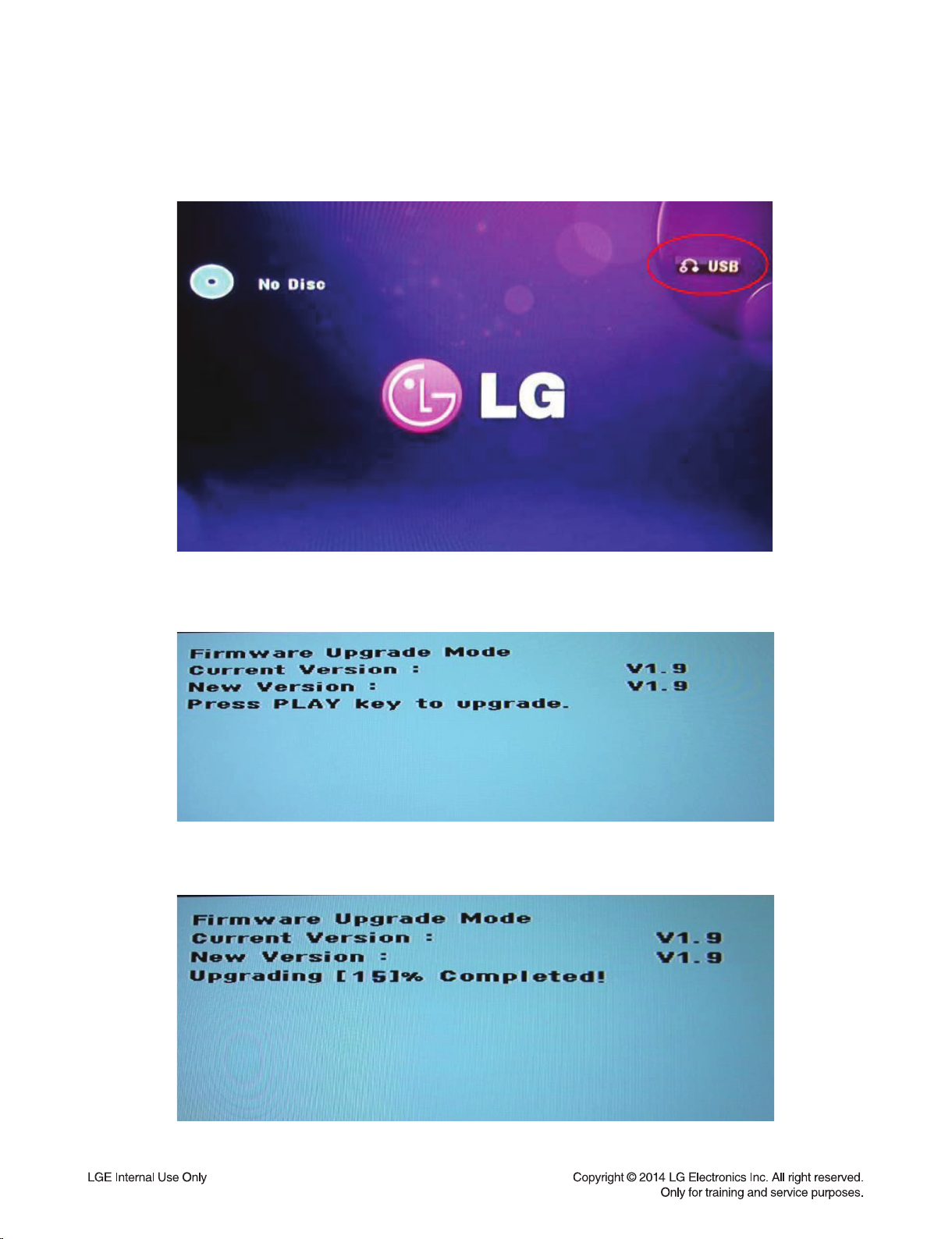
8. Insert the copied USB memory stick or Disc to DVD-player.
9. Press the RETURN button on the DVD Player. (USB only)
10. If the below picture appears on the screen. Press “PLAY” button on Remote controller.
While this menu appears, please don’t eject disc or take out USB.
11. After the below picture appears on the screen. New DVD program will download from USB
Memory stick or Disc automatically. Do not eject or take out the USB memory stick.
1-6
Page 8
12. After USB download is completed, DVD-player displays below picture automatically.
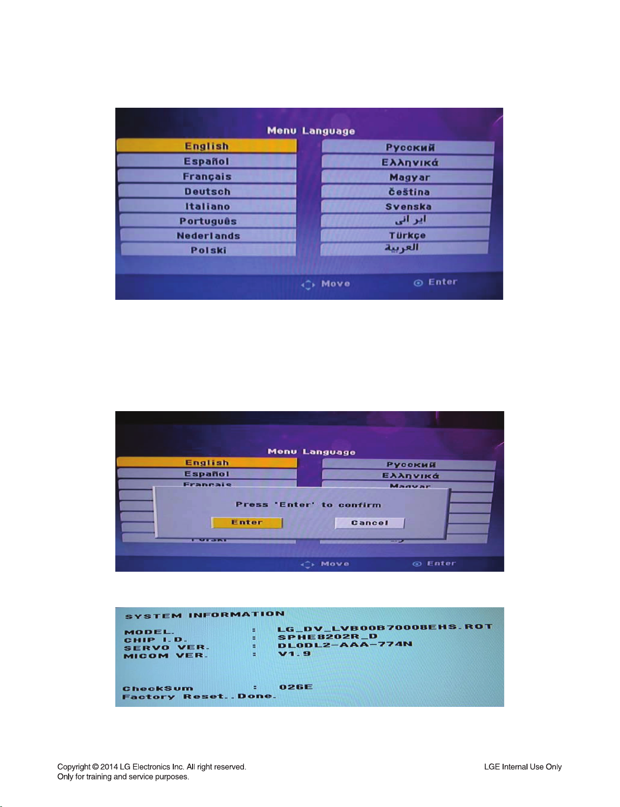
13. Do power off of DVD-Player.
14. Remove the Disc or USB memory stick.
15. Turn on the DVD-player.
Select the initial Language and Press “Enter” button.
Then, Select “Enter” and Press “Enter” button.
16. Do it again the process 1, 2, 3, 4 to confi rm the version.
17. Do power off of DVD-Player again.
1-7
Page 9

SPECIFICATIONS
Power requirements AC 110 - 240 V, 50 / 60 Hz
Power consumption 9 W
Dimensions (W x H x D) (360 x 39.5 x 200) mm
Net Weight (Approx.) 1.14 kg
Operating temperature 0 °C - 40 °C
Operating humidity 5 % - 90 %
Laser Semiconductor laser
Signal system PAL / NTSC
Bus Power Supply (USB) DC 5 V 200 mA
VIDEO OUT 1.0 V (p-p), 75 Ω, sync negative, RCA jack x 1
COMPONENT VIDEO OUT (Y) 1.0 V (p-p), 75 Ω, sync negative, RCA jack x 1,
(Pb)/(Pr) 0.7 V (p-p), 75 Ω, RCA jack x 2
ANALOG AUDIO OUT 2.0 Vrms (1 kHz, 0 dB), 600 Ω, RCA jack (L, R) x 1
DIGITAL AUDIO OUT (COAXIAL) 0.5 V (p-p), 75 Ω, RCA jack x 1
Note : Design and specifications are subject to change without prior notice.
1-8
Page 10

SECTION 2
CABINET & MAIN CHASSIS
CONTENTS
EXPLODED VIEWS ......................................................................................................................................... 2-2
1. CABINET AND MAIN FRAME SECTION ................................................................................................. 2-2
2. PACKING ACCESSORY SECTION ......................................................................................................... 2-3
2-1
Page 11
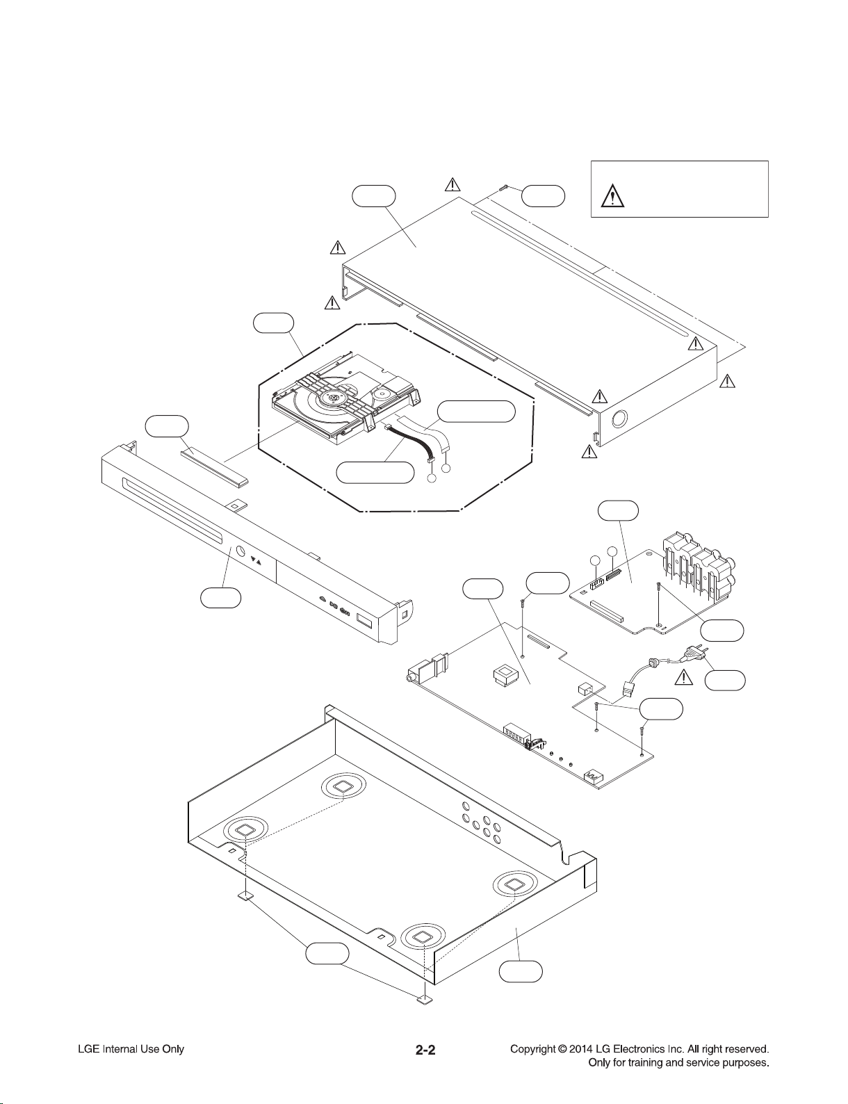
EXPLODED VIEWS
1. CABINET AND MAIN FRAME SECTION
A26
CABLE1
283
NOTES) THE EXCLAMATION POINT WITHIN AN
EQUILATERAL TRIANGLE IS INTENDED
TO ALERT THE SERVICE PERSONNEL
455250
TO THE PRESENCE OF IMPORTANT
SAFETY INFORMATION IN SERVICE
LITERATURE.
A43
CABLE2
A
B
A47
KARAOKE & MIC BOARD
SMPS & FRONT
BOARD
455
B
A46
A
MAIN
BOARD
455
300
455
261
260
Page 12
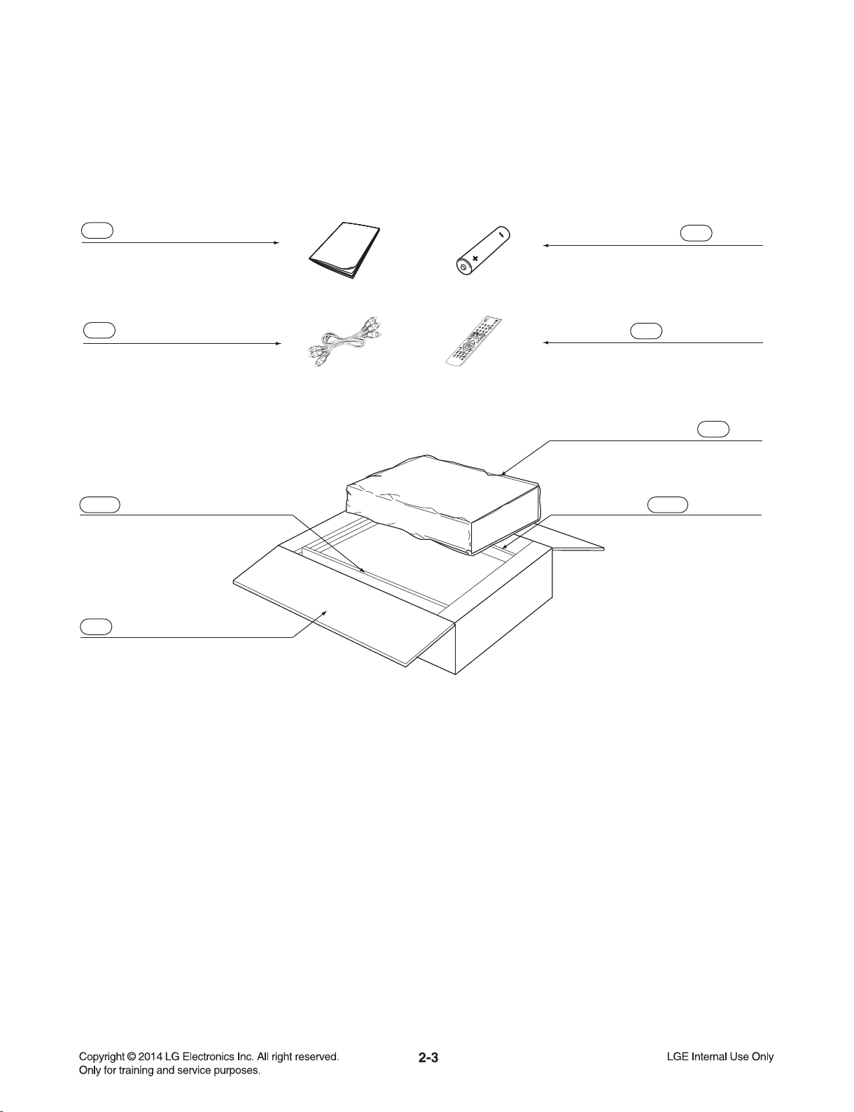
2. PACKING ACCESSORY SECTION
801 Owner’s manual
813 RCA Video/Audio cable
802A Pad (Front) 802B Pad (Rear)
802 Box
900 Remote control
808 Battery
804 Bag
Page 13

MEMO
2-4
Page 14

SECTION 3
ELECTRICAL
CONTENTS
ONE POINT REPAIR GUIDE ...............................................................................................3-2
1. NO BOOTING WHEN YOU TURN THE UNIT ON ................................................................................. 3-2
2. NO VIDEO OUTPUT WHEN YOU TURN THE UNIT ON ...................................................................... 3-7
3. NO AUDIO OUTPUT WHEN YOU TURN THE UNIT ON ...................................................................... 3-8
ELECTRICAL TROUBLESHOOTING GUIDE ......................................................................3-9
1. SMPS TROUBLESHOOTING FLOW ..................................................................................................... 3-9
2. POWER CHECK FLOW ....................................................................................................................... 3-10
3. SYSTEM OPERATION FLOW .............................................................................................................. 3-11
4. SYSTEM TEST FLOW .......................................................................................................................... 3-12
DETAILS AND WAVEFORMS ON SYSTEM TEST AND DEBUGGING ..........................3-18
1. SYSTEM 27 MHz CLOCK, RESET, FLASH R/W SIGNAL .................................................................. 3-18
2. SLED CONTROL RELATED SIGNAL (NO DISC CONDITION) .......................................................... 3-20
3. LENS CONTROL RELATED SIGNAL (NO DISC CONDITION) .......................................................... 3-20
4. LASER POWER CONTROL RELATED SIGNAL ................................................................................. 3-21
5. SPINDLE CONTROL WAVEFORM ...................................................................................................... 3-22
6. FOCUS ON WAVEFORM ..................................................................................................................... 3-22
7. TRACKING CONTROL RELATED SIGNAL (SYSTEM CHECKING) ................................................... 3-23
8. SPHE8202RQ-D AUDIO COAXIAL OUTPUT (SPDIF) ........................................................................ 3-24
9. SPHE8202RQ-D VIDEO OUTPUT WAVEFORM ................................................................................. 3-24
10. AUDIO OUTPUT FROM SPHE8202RQ-D/128 .................................................................................... 3-25
WIRING DIAGRAM .............................................................................................................3-26
CIRCUIT DIAGRAMS .........................................................................................................3-27
1. SMPS & FRONT - SMPS CIRCUIT DIAGRAM .................................................................................... 3-27
2. SMPS & FRONT - FRONT CONTROL CIRCUIT DIAGRAM ............................................................... 3-29
3. SMPS & FRONT - MIC CIRCUIT DIAGRAM (OPTIONAL PART) ....................................................... 3-31
4. MAIN - POWER SUPPLY/ OPU CIRCUIT DIAGRAM.......................................................................... 3-33
5. MAIN - SPHE8202RQ-D/ FLASH/ SDRAM CIRCUIT DIAGRAM ........................................................ 3-35
6. MAIN - AUDIO AMPLIFIER/ AUDIO OUTPUT/ MUTE/ VIDEO BUFFER/
VIDEO OUTPUT CIRCUIT DIAGRAM ..................................................................................... 3-37
CIRCUIT VOLTAGE CHART ..............................................................................................3-39
1. MPEG & SDRAM .................................................................................................................................. 3-39
2. IC ........................................................................................................................................................... 3-40
3. TR ......................................................................................................................................................... 3-41
4. CAPACITOR ......................................................................................................................................... 3-41
5. CONNECTOR ....................................................................................................................................... 3-42
PRINTED CIRCUIT BOARD DIAGRAMS ..........................................................................3-43
1. SMPS & FRONT P.C.BOARD .............................................................................................................. 3-43
2. MAIN P.C.BOARD ................................................................................................................................ 3-47
3-1
Page 15
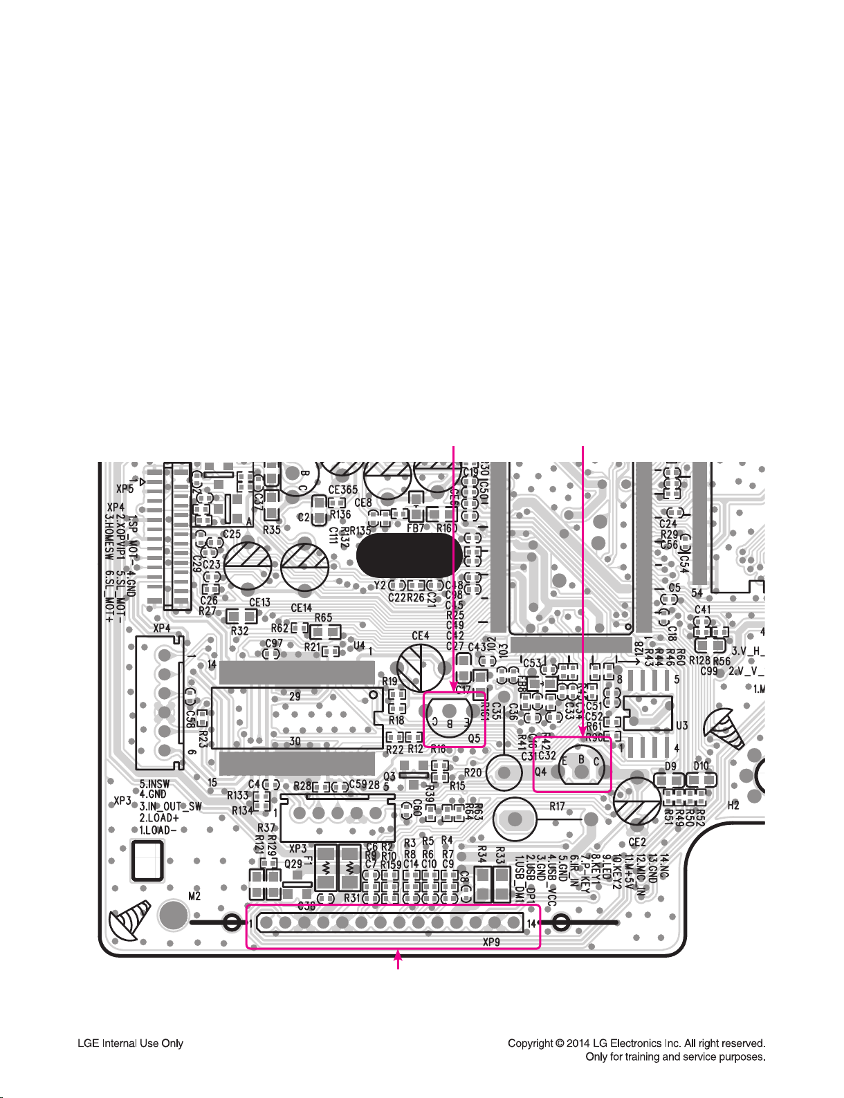
ONE POINT REPAIR GUIDE
1. NO BOOTING WHEN YOU TURN THE UNIT ON
When you plug power cord and turn the unit on, LED light won’t turn red, the unit won’t
read disc normally.
1-1. Please check every output voltage.
1-1-1. Please check if output voltage 3.3 V from main board Q4 C polarity is normal.
If output voltage 3.3 V is not normal, please check the working status of SMPS board.
1-1-2. Please check if output voltage 5 V from main board XP9 pin11 is normal.
If output voltage 5 V is not normal, please check the working status of SMPS board.
1-1-3. Please check if output voltage 1.2 V from main board Q5 C polarity is normal.
If output voltage 1.2 V is not normal, please check the working status of main board Q5.
Q5 Q4
XP9
< Main board top view >
3-2
Page 16
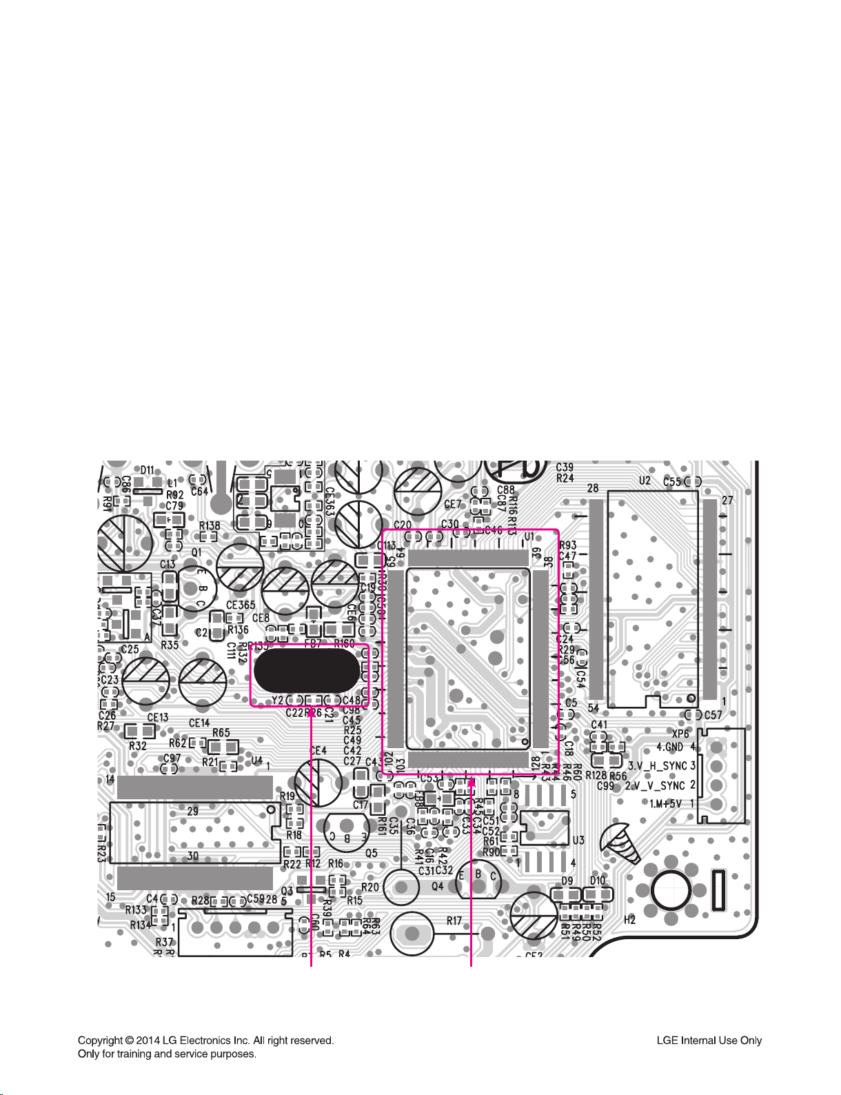
ONE POINT REPAIR GUIDE
When you plug power cord and turn the unit on, LED light won’t turn red, the unit won’t
read disc normally
1-2. Please check main board IC U1 signal and its peripheral circuit.
1-2-1. Please check if output voltage 3.3 V from U1 pin4, pin32, pin78, pin83 is normal.
If output voltage 3.3 V is not normal, please check 3.3 V power circuit of main board.
1-2-2. Please check if output voltage 1.2 V from U1 pin10, pin77, pin86 is normal.
If output voltage 1.2 V is not normal, please check 1.2 V power circuit of main board.
1-2-3. Please check if oscillating frequency 27 MHz of main board Y2 crystal is normal.
If oscillating frequency 27 MHz is not normal, please check if Y2 and its peripheral circuit is in failure.
1-2-4. Please check if frequency 135 MHz of U1 pin31 RAM_CLK is normal.
If oscillating frequency 135 MHz is not normal, please check if U1 is in failure.
.
Y2 U1
< Main board top view >
3-3
Page 17

ONE POINT REPAIR GUIDE
When you plug power cord and turn the unit on, LED light won’t turn red, the unit won’t
read disc normally.
1-3. Please check main board IC U2 signal and its peripheral circuit.
1-3-1. Please check if output voltage 3.3 V from IC U2 pin1, 3, 9, 14, 27, 43, 49 is normal.
If output voltage 3.3 V is not normal, please check 3.3 V power circuit of main board.
1-3-2. Please check every signal connected between IC U2 and IC U1, especially including DATA and
ADDRESS signal.
If DATA and ADDRESS signal is not normally output, please check if U2 is in failure.
U1 U2
< Main board top view >
3-4
Page 18

ONE POINT REPAIR GUIDE
When you plug power cord and turn the unit on, LED light won’t turn red, the unit won’t
read disc normally.
1-4. Please check main board IC U3 signal and its peripheral circuit.
1-4-1. Please check if output voltage 3.3 V from IC U3 pin8 is normal.
If output voltage 3.3 V is not normal, please check 3.3 V power circuit of main board.
1-4-2. Please check every signal connected between IC U3 and IC U1, especially including CE, DATA
and CLK signal.
If CE, DATA and CLK signal is not normally output, please check if U3 is in failure.
U1 U3
< Main board top view >
3-5
Page 19

ONE POINT REPAIR GUIDE
When you plug power cord and turn the unit on, LED light won’t turn red, the unit won’t
read disc normally.
1-5. Please check main board IC U4 signal and its peripheral circuit.
1-5-1. Please check if output voltage 5 V from U4 pin8, pin19 is normal.
If output voltage 5 V is not normal, please check 5 V power circuit of main board.
1-5-2. Please check every signal connected between IC U4 and IC U1, especially including F+, F-,
T+, T-, SP+, SP-, SL+, SL- signal to drive MD.
If F+, F-, T+, T-, SP+, SP-, SL+, SL- signal is not normally output, please check if U4 is in failure.
< Main board top view >
3-6
U1U4
Page 20

ONE POINT REPAIR GUIDE
2. NO VIDEO OUTPUT WHEN YOU TURN THE UNIT ON
When you plug power cord and turn the unit on, LED light will turn red, the unit will read
disc normally, but it won’t have video output.
2-1. Please check the solder joint status of main board connector P2.
2-2. Please check CVBS signal of main board IC U1 pin69.
If CVBS signal is not normally output, please check if U1 is in failure.
P2
U1
< Main board top view >
3-7
Page 21

ONE POINT REPAIR GUIDE
3. NO AUDIO OUTPUT WHEN YOU TURN THE UNIT ON
When you plug power cord and turn the unit on, LED light will turn red, the unit will read
disc normally, but it won’t have audio output.
3-1. Please check the solder joint status of main board connector P2.
If P2 has cold solder joint, P2 pins should be oxidated, and please replace P2.
3-2. Please check the working status of main board IC U927.
If output voltage 5 V from U927 pin7 is not normal, please check 5 V power circuit of main board.
If AL and AR signal from U927 pin1, pin2, pin9, pin10 is not normally output, please check if U927
is in failure.
3-3. Please check the working status of main board IC U1.
If AL and AR signal from U1 pin65, pin66 is not normally output, please check if U1 is in failure.
P2U927
U1
< Main board top view >
3-8
Page 22

ELECTRICAL TROUBLESHOOTING GUIDE
1. SMPS TROUBLESHOOTING FLOW
No +5 V
YES
Is the F501(T2AL) normal?
YES
Is the D501/ D502/ D503/ D504
normal?
YES
Is the U501(TNY176) normal?
YES
Is the D508 normal?
YES
Is there about 2.5 V
at the U503 Pin1?
NO
NO
NO
NO
NO
Replace the F501.
(Use the same ICW)
Replace the D501/ D502/ D503/ D504.
Replace the U501.
Replace the D508.
Replace the U503.
YES
Is the U502 normal?
YES
Power line of main PCB(DVD) is short.
NO
Replace the U502.
3-9
Page 23

ELECTRICAL TROUBLESHOOTING GUIDE
2. POWER CHECK FLOW
No 3.3 V No 1.2 V
Is M5V
supplied to Q4
emitter?
YES
Check or replace Q4.
NO
Replace the R17(1.8R/2W).
Replace the R20(5.6R/1W).
NO
NO
Is M5V
supplied to Q5
emitter?
YES
Is M5V
supplied to Q5
collector?
YES
Check or replace Q5.
3-10
Page 24

ELECTRICAL TROUBLESHOOTING GUIDE
3. SYSTEM OPERATION FLOW
Power on
1. MCU initializes SERVO, DSP & RISC registers.
2. Write RISC code to SDRAM.
3. Reset RISC.
Show “HELLO”
YES
Tray closed?
NO
Tray close to closed position.
SLED at inner side?
NO
SLED moves to inner position.
1. Judge whether have disc and disc type.
2. Jump to related disc reading procedure.
Recieve OPEN/ CLOSE key?
YES
YES
NO
NO
1. Execute pressed Key & IR key.
2. System operation routine loop.
1. Stop playback & open tray.
2. Display tray open message & LOGO.
Receive CLOSE key?
3-11
YES
Page 25

ELECTRICAL TROUBLESHOOTING GUIDE
4. SYSTEM TEST FLOW
TEST
Check the AC
voltage power PCBA.
YES
Make sure the main PCBA don’t short.
Power PCBA connected to AC voltage.
Is the DC
voltage outputs OK?
(5 V)
YES
Is 3.3 V
and 1.2 V DC outputs normal
on main PCBA?
YES
NO
Replace power PCBA.
NO
Repair or replace main PCBA.
NO
Repair or replace power PCBA.
NO
Check or replace Q4 or Q5.
Connect to PC RS232 cable and
update the FLASH memory code.
Update FLASH
successfully?
YES
A
NO
3-12
1. Check 27 MHz system clock.
2. Check system reset circuit.
3.
Check FLASH R/W enable signal WR, HOLD.
4. Check RS232 signals.
5. Check flash memory related circuit.
Page 26

ELECTRICAL TROUBLESHOOTING GUIDE
A
RESET or power on.
Show “SET”?
YES
Set language.
YES
NO NO
connection to TV set.
Flash
memory operates
properly?
YES
SPHE8202RQ-D
VIDEO outputs
properly?
YES
Have TV
signal output?
YES
Check AV cable
NO
NO
Check connection lines
between FLASH &
SPHE8202RQ-D and the
FLASH access time whether is
suitable or not.
Check the related circuit
of SPHE8202RQ-D.
Check the filtering and
amp circuit of TV signal.
Does
tray move inside
when it is not at closed
position?
YES
B
NO
OPEN_SW & CLOSE_
Normal
SW signals?
YES
Normal
OPEN & CLOSE
signal?
YES
Normal
FAN_TRAY+ & FAN_
TRAY- signal?
YES
Check the cable connection
between main PCBA and loader.
3-13
NO
NO
NO
Check the load
OPEN & CLOSE switch.
Check the tray control IO pins
on SPHE8202RQ-D & AM5890S.
Check the tray control
amplifying circuit on motor driver.
Page 27

ELECTRICAL TROUBLESHOOTING GUIDE
B
Does
the SLED move
to inner side when it is
at outter position?
YES
Do not put in disc
and tray close.
Motor
driver DMEA
Pin is High?
YES
Is SPDCO
DC Level Higher
than 1.65 V?
YES
SP+
& SP- output
properly?
YES
Check the cable
connection with mechanism.
NONO
NO
NO
Check the connection
line of DMEA signal.
Check the related circuit
of SCO.
Check the amp circuit
on motor driver.
Optical Lens
has movements for
searching
focus?
YES
C
Proper
FCO outputs to
motor driver?
YES
Proper
FOC+ & FOC-
outputs?
YES
Check cable connect on
with pick-up head.
3-14
NONO
NO
Check FCO connection
on SPHE8202RQ-D
and motor driver.
Check the amp circuit
on motor driver.
Page 28

ELECTRICAL TROUBLESHOOTING GUIDE
C
Laser
turns on when
reading disc?
YES
Put disc in?
YES
Disc ID
is correct?
NO NO
NO
NO
DVDLDO,
CDLDO output
properly?
YES
Collector
voltage of power
transistor is OK?
YES
Check cable connection
between transistor ouput
and pick-up head.
Laser off.
Proper PUHRF
signal on OPU.
YES
NO
NO
Check the laser power circuit
on SPHE8202RQ-D and
connedting to power transistor.
Check the related circuit
on laser power transistor.
Check the related circuit
on PUHRF signal.
YES
Does
spindle rotate?
YES
D
Check DVDLDO &
CDLDO signal.
NO NO
between spindle and main PCBA.
Proper SCO signal
on SPHE8202RQ-D.
YES
SLED+
& SLED- output
properly?
YES
Check the cable connection
NO
3-15
Check SCO related circuit
on SPHE8202RQ-D.
Check the spindle control
amp circuit of motor driver.
Page 29

ELECTRICAL TROUBLESHOOTING GUIDE
D
Focus on OK?
YES
Track on OK?
NO NO
signals on A, B, C, D of
Check cable connection
NO NO
Proper
SPHE8202RQ-D.
YES
Check FCO signal
on SPHE8202RQ-D.
YES
FOC+ & FOC-
output properly?
YES
on pick-up head.
Properly TCO signal
on SPHE8202RQ-D?
YES
NO
NO
Check connections
between SPHE8202RQ-D
and pick-up head.
Check the FCO connection
on SPHE8202RQ-D
and motor driver.
Check the focus control
amp circuit on motor driver
Check the TCO connection
on SPHE8202RQ-D
and motor driver.
YES
Disc is play?
YES
E
NO
RAD+ & RAD-
output properly?
YES
Check cable connection
on pick-up head.
Check PUHRF
signal waveform.
3-16
NO
Check the tracking control
amp circuit on motor driver.
Page 30

ELECTRICAL TROUBLESHOOTING GUIDE
E
Normal
audio output when
disc playback?
YES
Normal
IR.VFD & front panel key
functions?
YES
NO
NO NO
AMP received correct
between IR.VFD front panel key
Audio
data stream?
YES
Normal
audio AMP out?
YES
Check audio filter,
amplify, mute circuit.
Communications
& SPHE8202RQ-D is
normally?
YES
NO
NO
Check connection between
SPHE8202RQ-D & audio AMP.
Check the related
circuit of audio AMP.
Check communication lines
on SPHE8202RQ-D.
Test end.
Check the cable connection
on front panel.
3-17
Page 31

DETAILS AND WAVEFORMS ON SYSTEM TEST AND DEBUGGING
1. SYSTEM 27 MHz CLOCK, RESET, FLASH R/W SIGNAL
1) SPHE8202RQ-D main clock is at 27 MHz (Y2)
1
2) SPHE8202RQ-D reset is active high.
FIG 1-1
3.3V
1
CLKOUT CLKIN
R25 75R25 75
Y2
Y2
R26 100KR26 100K
C21
C21
33pF/50V/NP0
33pF/50V/NP0
GND
27MHz/30PPM
27MHz/30PPM
C22
C22
33pF/50V/NP0
33pF/50V/NP0
RESET
R56
R56
27K
27K
DVCC3
GND
R128 1KR128 1K
C99
C99
2.2uF/10V/Y5V
2.2uF/10V/Y5V
TP17TP17
C41
C41
0.1uF/25V/Y5V
0.1uF/25V/Y5V
4
RESET1
3
PCON/LED
TP71TP71
R16 4.7KR16 4.7K
R15
R15
4.7K
4.7K
Q3
Q3
NPN_3DG3904M
NPN_3DG3904M
GND
2
2
POCN
RESET
3
4
FIG 1-2
3-18
Page 32

3) RS232 waveform during procedure (Downloading)
5
6
TXD
RXD
FIG 1-3
4) Flash CE# enable signal and SCK signal during Downloading
M+5V
Debug Port
V_V_SYNC
V_H_SYNC
GND
TP47TP47
TP48TP48
5 6
TP46TP46
TP45TP45
XP6
XP6
1
1
2
2
3
3
4
4
4PIN/2.0mm
4PIN/2.0mm
7
8
CS
SCK
DVCC3 DVCC3
R90 10KR90 10K
R61 10KR61 10K
C52
C52
0.1uF/25V/Y5V
0.1uF/25V/Y5V
GND
7 8
U3
U3
1
SPI_CE
2
SPI_D0
3
4
GND GND
8
CE#
VDD
7
SO
HOLD#
6
WP#
SCK
5
VSS
SI
SPI_16Mb_EN25T160
SPI_16Mb_EN25T160
SPI_CLK
SPI_D1
C51
C51
0.1uF/25V/Y5V
0.1uF/25V/Y5V
FIG 1-4
3-19
Page 33

2. SLED CONTROL RELATED SIGNAL (NO DISC CONDITION)
U4
1
9
10
11
12
FIG 2-1
M+5V
GND
C97
C97
0.1uF/25V/Y5V
0.1uF/25V/Y5V
SP_MOT+
XOPVIP1
XOPVIN1
FOCUS_S
TR_B1
REGO2
SPDL_S TR_B2
10
REGO1
11
LOAD-
9
SP_MOT-
R65 1R65 1
VINFC
2
TR_B1
3
REGO2
4
VINSL
5
REGO1
6
SL-
FWD
7
SL+
REV
29
GND
8
VCC1
9
VOTR-
10
VOTR+
11
VOSL+
12
VOSL-
13
FACT-
VOFC-
14
FACT+
VOFC+
AM5890SU4AM5890S
MUTE
BIAS
VINTK
TR_B2
RESET
VINLD
GND
GND
VCTL
VCCD
VCC2
VOLD-
VOLD+
VOTK-
VOTK+
12
28
27
26
25
24
23
22
30
21
20
19
18
17
16
15
TP50TP50
DRVSB
DRVSB
VREF2
TRACK_S
RESET
SLED_S
GNDGND
SL_MOT+
SL_MOT-
TACT-
TACT+
3. LENS CONTROL RELATED SIGNAL (NO DISC CONDITION)
FOCUS_S
TR_B1
13
14
15
FIG 3-1
M+5V
GND
C97
C97
0.1uF/25V/Y5V
0.1uF/25V/Y5V
SP_MOT+
XOPVIP1
XOPVIN1
REGO2
SPDL_S TR_B2
REGO1
SL-
SL+
LOAD-
SP_MOT-
R65 1R65 1
FACT-
FACT+
1415
13
TP50TP50
U4
1
VINFC
2
TR_B1
3
REGO2
4
VINSL
5
REGO1
6
FWD
7
REV
29
GND
8
VCC1
9
VOTR-
10
VOTR+
11
VOSL+
12
VOSL-
13
VOFC-
14
VOFC+
AM5890SU4AM5890S
MUTE
BIAS
VINTK
TR_B2
RESET
VINLD
GND
GND
VCTL
VCCD
VCC2
VOLD-
VOLD+
VOTK-
VOTK+
28
DRVSB
DRVSB
27
VREF2
26
TRACK_S
25
24
RESET
23
SLED_S
22
30
21
GNDGND
20
19
18
SL_MOT+
17
SL_MOT-
16
TACT-
15
TACT+
3-20
Page 34

4. LASER POWER CONTROL RELATED SIGNAL
7
7
16
17
18
GND
XP5
XP5
27
28
24PIN/0.5mm
24PIN/0.5mm
24
23
22
FIG 4-1 (NO DISC CONDITION)
16
17
18
21
20
19
18
17
16
15
14
13
12
TOP
TOP
11
10
9
8
7
6
5
4
3
2
1
25
26
TP20TP20
GND
TP44TP44
FACTFACT+
TACT+
TACT-
TP43TP43
TP42TP42
C
D
TP56TP56
TP63TP63
TP57TP57 C37
TP65TP65
TP66TP66
TP62TP62
TP67TP67
PUHRF
A
B
F
TP61TP61
TP55TP55
TP58TP58
GND
TP64TP64
TP59TP59
VREF1
E
CDVR#
DVDVR#
PUH_CDLD
DVDMDI
PUH_DVDLD
C29
C29
0.1uF/25V/Y5V
0.1uF/25V/Y5V
0.1uF/25V/Y5V
0.1uF/25V/Y5V
P+5V
R27
R27
10K
10K
TP5TP5
P+5V
C23 0.1uF/25V/Y5VC23 0.1uF/25V/Y5V
C25 0.1uF/25V/Y5VC25 0.1uF/25V/Y5V
R36 100R36 100
R38 100R38 100
16
GND
C37
GND
CDLDO
PNP_MMBT8550CLT1
PNP_MMBT8550CLT1
TP8TP8
LDSW
TRAY-
C11
C11
1000pF/50V/X7R
1000pF/50V/X7R
GND
TP9TP9
RF3.3V
CE13
CE13
+
+
47uF/16V
47uF/16V
CDVR
DVDVR
DVDMDI
CDMDI
C12
C12
1000pF/50V/X
1000pF/50V/X
GND
R47
R47
5.1
5.1
Q9
Q9
GND
16
17
18
FIG 4-2 (CD)
FIG 4-3 (DVD)
3-21
17
0.1uF/25V/Y5V
0.1uF/25V/Y5V
5V
C37
C37
GND
PNP_MMBT8550CLT1
PNP_MMBT8550CLT1
TP8TP8
TP9TP9
RF3.3V
CE13
CE13
+
+
47uF/16V
47uF/16V
Q9
Q9
R47
R47
5.1
5.1
RF3.3V
R48
R48
+
+
5.1
5.1
Q10
Q10
PNP_MMBT8550CLT1
PNP_MMBT8550CLT1
TP6TP6
CE14
CE14
47uF/16V
47uF/16V
TP7TP7
DVDLDOCDLDO
18
Page 35

5. SPINDLE CONTROL WAVEFORM
19
20
21
6. FOCUS ON WAVEFORM
FIG 5-1
M+5V
GND
C97
C97
0.1uF/25V/Y5V
0.1uF/25V/Y5V
SP_MOT+
XOPVIP1
XOPVIN1
FOCUS_S
TR_B1
REGO2
SPDL_S TR_B2
19
REGO1
20
LOAD-
21
SP_MOT-
R65 1R65 1
VINFC
2
TR_B1
3
REGO2
4
VINSL
5
REGO1
6
SL-
FWD
7
SL+
REV
29
GND
8
VCC1
9
VOTR-
10
VOTR+
11
VOSL+
12
VOSL-
13
FACT-
VOFC-
14
FACT+
VOFC+
AM5890SU4AM5890S
U4
1
MUTE
VINTK
TR_B2
RESET
VINLD
VCTL
VCCD
VCC2
VOLD-
VOLD+
VOTK-
VOTK+
BIAS
GND
GND
TP50TP50
28
DRVSB
DRVSB
27
VREF2
26
TRACK_S
25
24
RESET
23
SLED_S
22
30
21
GNDGND
20
19
18
SL_MOT+
17
SL_MOT-
16
TACT-
15
TACT+
22
23
24
22
23
24
FIG 6-1 (CD)
M+5V
GND
C97
C97
0.1uF/25V/Y5V
0.1uF/25V/Y5V
SP_MOT+
XOPVIP1
XOPVIN1
22
U4
1
FOCUS_S
TR_B1
REGO2
SPDL_S TR_B2
REGO1
LOAD-
SP_MOT-
R65 1R65 1
VINFC
2
TR_B1
3
REGO2
4
VINSL
5
REGO1
6
SL-
FWD
7
SL+
REV
29
GND
8
VCC1
9
VOTR-
10
VOTR+
11
VOSL+
12
VOSL-
13
FACT-
VOFC-
14
FACT+
VOFC+
AM5890SU4AM5890S
2423
MUTE
BIAS
VINTK
TR_B2
RESET
VINLD
GND
GND
VCTL
VCCD
VCC2
VOLD-
VOLD+
VOTK-
VOTK+
TP50TP50
28
DRVSB
DRVSB
27
VREF2
26
TRACK_S
25
24
RESET
23
SLED_S
22
30
21
GNDGND
20
19
18
SL_MOT+
17
SL_MOT-
16
TACT-
15
TACT+
FIG 6-2 (DVD)
3-22
Page 36

7. TRACKING CONTROL RELATED SIGNAL (SYSTEM CHECKING)
25
26
27
TP50TP50
MUTE
BIAS
VINTK
TR_B2
RESET
VINLD
GND
GND
VCTL
VCCD
VCC2
VOLD-
VOLD+
VOTK-
VOTK+
25
28
DRVSB
DRVSB
27
VREF2
26
TRACK_S
25
TR_B2
24
RESET
23
SLED_S
22
30
21
GND
20
19
18
SL_MOT+
17
SL_MOT-
16
TACT-
15
TACT+
26 27
C4 0.1uF/25V/Y5VC4 0.1uF/25V/Y5V
R22 0R22 0
R23 0R23 0
GND
SL-
SL+
25
FIG 7-1 (CD)
U4
1
VINFC
2
TR_B1
3
REGO2
4
VINSL
5
REGO1
6
FWD
7
REV
29
GND
8
VCC1
9
VOTR-
10
VOTR+
11
VOSL+
12
VOSL-
13
VOFC-
14
VOFC+
AM5890SU4AM5890S
RESET CIRCUIT
M+5V
R1331KR133
1K
R1343KR134
3K
GND
26
27
FIG 7-2 (DVD)
3-23
Page 37

8. SPHE8202RQ-D AUDIO COAXIAL OUTPUT (SPDIF)
TP68TP68
SPDIF_OUT
R113
R113
28
200
200
C87
C87
R116
R116
0.1uF/25V/Y5V
0.1uF/25V/Y5V
100
28
FIG 8-1
100
GND
SPDIF Circuit
FB9 500/800mAFB9 500/800mA
C88
C88
10pF/50V/NP0
10pF/50V/NP0
COAX
C114
C114
47pF/50V/NP0
47pF/50V/NP0
9. SPHE8202RQ-D VIDEO OUTPUT WAVEFORM
1) 100% COLOR BAR
FIG 9-1
3-24
Page 38

10. AUDIO OUTPUT FROM SPHE8202RQ-D/128
FIG 10-1
3-25
Page 39

WIRING DIAGRAM
DVD LOADER
TDL-5 LOADER+Doree TDT-DM00
SPSP+
HOMESW
GND
SLSL+
INSW
GND
1
24
1
6
1
XP3 XP4 XP5
2
6PIN*2.0 24PIN*0.5
2PIN*2.0
P1
AUDIO & VIDEO
MOTER
DRIVER
AM5890S
COAXFR
CVBS
FL
AMP&LPF
SPHE8202RQ-D
14PIN*2.0
XP2
1
Pb Pr
Y
M12L64164A
12
64M
16M SPI
FLASH
EN25T1
SDRAM
MAIN BOARD
USB_DP
USB_DM
GND
USB_5V
GND
IR
powerKEY
DATA
CLOCK
STB
M5V
MIC
12 1
XS301
12PIN*2.0
KEY+USB+MIC+LED
PI176
3-26
Page 40

A
1
2
3
4
5
6
7
8
9
10
11
12
B C D E F G H I J K L M N O P Q R ST
AC INPUT
GND1
HV1 HV2
GND2
HV1
GND1
GND2
HV2
GND_POWER
<IREF>
+5V
<IREF>
+12V
<IREF>
F501
10ohm/2W
F501
10ohm/2W
ZD501
BZX79C11
ZD501
BZX79C11
R501 10KR501 10K
T501
36-TRF325-XX0-M
T501
36-TRF325-XX0-M
10
11
1
4
6
8
2
9
7
+
470uF/16V
CE507
+
470uF/16V
CE507
L501
680uH/300mA
L501
680uH/300mA
+
C505
NC 47uF/25V
+
C505
NC 47uF/25V
D501
1N4007/1A/1000V
D501
1N4007/1A/1000V
D506
FR104/1A/400V
D506
FR104/1A/400V
D505
1N4007/1A/1000V
D505
1N4007/1A/1000V
R510 10KR510 10K
C502 0.1uF/63VC502 0.1uF/63V
+
10uF/50V
CE503
+
10uF/50V
CE503
FB501
FB80@100MHz
FB501
FB80@100MHz
U502
LTV-817S-B
U502
LTV-817S-B
12
43
C501
1500pF/1KV
C501
1500pF/1KV
CY501 1000pF/250VACCY501 1000pF/250VAC
+
15uF/450V
CE502
+
15uF/450V
CE502
R504
NC 10k
R504
NC 10k
R502
150K
R502
150K
+
10uF/50V
CE504
+
10uF/50V
CE504
R503
150K
R503
150K
U501
TNY177
U501
TNY177
S
8
EN/UV
1
S5S
6
Drain
4
S
7
NC
3
BP/M
2
+
1000uF/16V
CE506
+
1000uF/16V
CE506
L502 6.8uHL502 6.8uH
U503U503
3
1
2
R511
100K
R511
100K
R505
12K/1%
R505
12K/1%
D507
NC
FR104/1A/400V
D507
NC
FR104/1A/400V
D508
SR360/3A/60V
D508
SR360/3A/60V
R507
11.3K/1%
R507
11.3K/1%
CN501
2PIN/7.92mm
CN501
2PIN/7.92mm
1
1
2
2
R5081KR508
1K
LF501
NC/20mH
LF501
NC/20mH
R509 100R509 100
D502
1N4007/1A/1000V
D502
1N4007/1A/1000V
+
15uF/500V
CE501
+
15uF/500V
CE501
D504
1N4007/1A/1000V
D504
1N4007/1A/1000V
D503
1N4007/1A/1000V
D503
1N4007/1A/1000V
ZD502NCZD502
NC
Warning
Parts that are shaded are critical with
respect to risk of fire or electrical shock.
3-27 3-28
CIRCUIT DIAGRAMS
1. SMPS & FRONT - SMPS CIRCUIT DIAGRAM
WHEN SERVICING THIS CHASSIS, UNDER NO
CIRCUMSTANCES SHOULD THE ORIGINAL
DESIGN BE MODIFIED OR ALTERED WITHOUT
PERMISSION FROM THE LG CORPORATION. ALL
COMPONENTS SHOULD BE REPLACED ONLY WITH
TYPES IDENTICAL TO THOSE IN THE ORIGINAL
CIRCUIT. SPECIAL COMPONENTS ARE SHADED
ON THE SCHEMATIC FOR EASY IDENTIFICATION.
THIS CIRCUIT DIAGRAM MAY OCCASIONALLY
DIFFER FROM THE ACTUAL CIRCUIT USED. THIS
WAY, IMPLEMENTATION OF THE LATEST SAFETY
AND PERFORMANCE IMPROVEMENT CHANGES
INTO THE SET IS NOT DELAYED UNTIL THE NEW
SERVICE LITERATURE IS PRINTED.
1. Shaded( ) parts are critical for safety. Replace only
with specified part number.
2. Voltages are DC-measured with a digital voltmeter
during Play mode.
IMPORTANT SAFETY
NOTE :
Page 41

A
1
2
3
4
5
6
7
8
9
10
11
12
B C D E F G H I J K L M N O P Q R ST
CLOSE ET6207
TO MAIN BORAD
Power
Open/Close
Play/Pause
Volumn Down
Volumn Up
KS4
KS3
SG3
KS2
KS1
SG5
SG6
SG7
SG8
GR5
GR4
GR3
GR2
GR1
KS5
KS6
KS3
KS5
KS6
KEY2
GR[1:5]
GR1
SG8
GR5
SG2
SG7
SG6
SG3
SG1
SG4
M5VL
VSDA
SG1
SG2
SG4
IR
VCC_USB
VSCK
VSTB
KEY1
osc
SG[1:8]
KS[1:6]
KS1
GND
GR4
GND_POWER
GND_POWER
KS2
MIC
+5V
VSDA
IR
GND
VCC_USB
GND_POWER
USB_DP
USB_DM
GR3
GR2
SG5
USB_DM
USB_DP
VSTB
VSCK
INSW
INSW
+5V
+5V
+5V
MIC
+5V
GND_POWER
+12V
<IREF>
+5V
R1421KR142
1K
USB
P301
USB
USB
P301
USB
1
2
3
4
5
6
7
8
XS3
14PIN/2.0mm
XS3
14PIN/2.0mm
1
1
2
2
3
3
4
4
5
5
6
6
7
7
8
8
9
9
10
10
11
11
12
12
13
13
14
14
+
47uF/16V
CE135
+
47uF/16V
CE135
S135
TAC041
S135
TAC041
R1 0R1 0
R139
4.7K
R139
4.7K
R135 1KR135 1K
S140
TAC041
S140
TAC041
R145 1KR145 1K
C167
1uF/10V/Y5V
C167
1uF/10V/Y5V
S136
TAC041
S136
TAC041
C306
NC/100pF/50V/NP0
C306
NC/100pF/50V/NP0
R144 10KR144 10K
R141 1KR141 1K
C137
100pF/50V/NP0
C137
100pF/50V/NP0C136
100pF/50V/NP0
C136
100pF/50V/NP0
S137
TAC041
S137
TAC041
R2 0R2 0
R143 51KR143 51K
R140
4.7K
R140
4.7K
R137 1KR137 1K
XS2
14PIN/2.0mm
XS2
14PIN/2.0mm
1
1
2
2
3
3
4
4
5
5
6
6
7
7
8
8
9
9
10
10
11
11
12
12
13
13
14
14
XP1
NC
2PIN/2.0mm
XP1
NC
2PIN/2.0mm
1
1
2
2
C307
NC/100pF/50V/NP0
C307
NC/100pF/50V/NP0
R138
4.7K
R138
4.7K
R167 470R167 470
R166
470
R166
470
LED1
LED_2501AHG1
LED1
LED_2501AHG1
GRID5
13
GRID4
12
GRID3
11
GRID2
10
GRID1
9
SEG8
8
SEG7
7
SEG6
6
SEG5
5
SEG4
4
SEG3
3
SEG2
2
SEG1
1
IR1
IRM_8.3mm
IR1
IRM_8.3mm
IR
1
GND
2
VCC
3
C135
100pF/50V/NP0
C135
100pF/50V/NP0
U135
DRIVER_LED_ETK6207
U135
DRIVER_LED_ETK6207
OSC
1
DI/O
2
CLK
3
STB
4
KEY2
5
VDD
6
SG1/KS1
7
SG2/KS2
8
SG3/KS3
9
SG4/KS4
10
GR2
19
GND
18
GR3
17
GR4
16
SG14/GR5
15
SG13/GR6
14
SG12/GR7
13
GR1
20
SG6/KS6
12
SG5/KS5
11
C166
47pF/50V/NP0
C166
47pF/50V/NP0
R136 1KR136 1K
S139
TAC041
S139
TAC041
C138
0.1uF/50V/Y5V
C138
0.1uF/50V/Y5V
3-29 3-30
2. SMPS & FRONT - FRONT CONTROL CIRCUIT DIAGRAM
Page 42

A
1
2
3
4
5
6
7
8
9
10
11
12
B C D E F G H I J K L M N O P Q R ST
3-31 3-32
3. SMPS & FRONT - MIC CIRCUIT DIAGRAM (OPTIONAL PART)
Page 43

9
21
1120
1019
12
25
26 27
14
24
15
23
2
16
18
17
3
: WAVEFORM NUMBER
A
1
2
3
4
5
6
7
8
9
10
11
12
B C D E F G H I J K L M N O P Q R ST
13
22
GND
GND
SP-
STANDBY:40mA
Imax: 570mA
SP+
STANDBY:25mA
Imax: 368mA
STANDBY:15mA
Imax: 202mA
HOMESW
INSW
SLEDSLED+
8202 kernel +1.2V
Servo analog +5V
RESET CIRCUIT
M+5V
+12V: +12V(+-10%)
+5V: +5V(+-2.5%)
TO FRONT PANEL
FROM POWER BOARD
GND
IR
KEY2(STB)
KEY1(DATA)
LED (CLOCK)
USB_DM
USB_DP
USB_VCC(protect)
Use INSW and GND for DOREE LAODER
GND
MIC
powerkey
SPDL_S TR_B2
TR_B1
REGO2
LDSW
HOMESW
INSW
IN_OUT_SW
SP_MOT+
REGO2
REGO1
TR_B2TR_B1
SL_MOT-
SL_MOT+
SP_MOT-
DVDMDI
PUHRF
DVDVR
CDVR
VREF1
CDMDI
DVDMDI
E
DVDVR#
TRAY-
DVDLDO
CDMDI
USB_POWER
PCON/LED
VREF1
IR_IN
F
E
DVDMDI
RESET
USB_POWER
CDLDO
DVDLDO
RESET
FACT+
FOCUS_S
XOPVIN1
XOPVIP1
SL_MOT-
SP_MOT+
SL_MOT+
LDSW
XOPVIP1
XOPVIN1
VREF2
A
B
IN_OUT_SW
C
HOMESW
SLED_S
FOCUS_S
INSW
DRVSB
SPDL_S
TRACK_S
FACT-
VREF2
TACT-
TRACK_S
D
REGO1
SLED_S
DRVSB
SP_MOT-
TACT+
LOAD-
USB_DM1
USB_DP1
USB_VCC
PCON/LED
USB_DM1
USB_VCC
VFD_CLK
VFD_DATA
VFD_STB
IR_IN
USB_DP1
CDVR#
DVDVR
CDVR
VFD_DATA
VFD_STB
VFD_CLK
SL-
SL-
LOAD-
SL+
SL+
CDLDO
FACTFACT+
TACT+
TACT-
C
D
PUHRF
A
B
F
PUH_CDLD
PUH_DVDLD
M+5V
MIC_IN
MIC_IN
M+5V
P+5V
POWERKEY
POWER_KEY
POWER_KEY
M+5V
DRVSB
M+5V
INSW
GND
GND
GND
GND
GND
DVCC3
GND
GND
M+5V
DVCC3
P+5V
GND
GND
GND
GND
GND
P+5V
GND
RF3.3V
RF3.3V
P+5V
GND
GND
GND
M+5V
GND
GND
GND
M+5V
DVCC3
GNDGND
M+5V
GND
GND
VCC1.2
CDVR
4
DVDVR
4
DVDMDI
4
PUHRF
4
CDMDI
4
VREF1
4
F
4
E
4
RESET
4
CDLDO
4
DVDLDO
4
USB_POWER
4
LDSW
4
SPDL_S
4
SLED_S
4
TRACK_S
4
FOCUS_S
4
XOPVIP1
4
HOMESW
4
XOPVIN1
4
A
4
IN_OUT_SW
4
VREF2
4
D
4
INSW
4
B
4
C
4
DRVSB
4
PCON/LED
4
VFD_CLK
4
VFD_DATA
4
VFD_STB
4
IR_IN
4
USB_DM1
4
USB_DP1
4
USB_VCC
4
MIC_IN
4
M+5V
5
P+5V
5
POWER_KEY
5
M+5V
4
R47
5.1
R47
5.1
C14
100pF/50V/NP0
C14
100pF/50V/NP0
TP65TP65
R10
4.7K
R10
4.7K
R16 4.7KR16 4.7K
TP34TP34
TP25TP25
TP64TP64
TP29TP29
TP43TP43
TP20TP20
TP66TP66
Q4
PNP_3CA8550C
Q4
PNP_3CA8550C
R8 220R8 220
TP5TP5
TP26TP26
C3
0.1uF/50V/Y5V
C3
0.1uF/50V/Y5V
TP42TP42
R17
1.8/2W
R17
1.8/2W
C25 0.1uF/25V/Y5VC25 0.1uF/25V/Y5V
R27
10K
R27
10K
C7
100pF/50V/NP0C7100pF/50V/NP0
TP62TP62
R18
20K/1%
R18
20K/1%
TP27TP27
R2
4.7KR24.7K
R48
5.1
R48
5.1
TP67TP67
R7 220R7 220
C29
0.1uF/25V/Y5V
C29
0.1uF/25V/Y5V
TP61TP61
Q10
PNP_MMBT8550CLT1
Q10
PNP_MMBT8550CLT1
TP21TP21
R37
3.3K
R37
3.3K
C58
1000pF/50V/X7R
C58
1000pF/50V/X7R
C6
100pF/50V/NP0
C6
100pF/50V/NP0
TP50TP50
TP35TP35
Q1
PNP_3CA8550D
Q1
PNP_3CA8550D
R35 0R35 0
C59
1000pF/50V/X7R
C59
1000pF/50V/X7R
R340R34
0
TP36TP36
R20 5.6/1WR20 5.6/1W
U4
AM5890SU4AM5890S
VINFC
1
VOTR-
9
VOTR+
10
VOSL-
12
REGO2
3
TR_B1
2
VOTK+
15
REV
7
VOFC+
14
VOFC-
13
VCTL
21
VCC2
19
VCCD
20
RESET
24
BIAS
27
FWD
6
VINSL
4
REGO1
5
MUTE
28
VCC1
8
VOSL+
11
VOLD+
17
VOLD-
18
VOTK-
16
VINLD
23
GND
22
TR_B2
25
VINTK
26
GND
29
GND
30
C17
0.1uF/50V/Y5V
C17
0.1uF/50V/Y5V
TP8TP8
XP4
6PIN/2.0mm
XP4
6PIN/2.0mm
1
1
2
2
3
3
4
4
5
5
6
6
R6 220R6 220
C12
1000pF/50V/X7R
C12
1000pF/50V/X7R
C60
1000pF/50V/X7R
C60
1000pF/50V/X7R
R62
4.7K
R62
4.7K
TP37TP37
TP40TP40
TP9TP9
R3
NC/4.7KR3NC/4.7K
TP18TP18
XP10
2PIN/2.0mm
XP10
2PIN/2.0mm
1
1
2
2
TP57TP57
R19
12K/1%
R19
12K/1%
C9
100pF/50V/NP0C9100pF/50V/NP0
TP6TP6
R65 1R65 1
C13
0.1uF/50V/Y5V
C13
0.1uF/50V/Y5V
R1591KR159
1K
TP70TP70
C37
0.1uF/25V/Y5V
C37
0.1uF/25V/Y5V
C10
100pF/50V/NP0
C10
100pF/50V/NP0
TP19TP19
R5
NC/4.7KR5NC/4.7K
+
47uF/16V
CE13
+
47uF/16V
CE13
TP63TP63
R933R9
33
TP7TP7
TP30TP30
R33 0R33 0
R4
NC/4.7KR4NC/4.7K
C4 0.1uF/25V/Y5VC4 0.1uF/25V/Y5V
R36 100R36 100
Q5
PNP_3CA8550C
Q5
PNP_3CA8550C
TP28TP28
Q9
PNP_MMBT8550CLT1
Q9
PNP_MMBT8550CLT1
R631KR63
1K
XP9
14PIN/2.0mm
XP9
14PIN/2.0mm
1
1
2
2
3
3
4
4
5
5
6
6
7
7
8
8
9
9
10
10
11
11
12
12
13
13
14
14
TOP
XP5
24PIN/0.5mm
TOP
XP5
24PIN/0.5mm
24
23
22
21
20
19
18
17
16
15
14
13
12
11
10
9
8
7
6
5
4
3
2
1
25
26
27
28
R22 0R22 0
TP69TP69
R1331KR133
1K
TP31TP31
R39 0R39 0
TP56TP56
R28 10KR28 10K
+
47uF/16V
CE14
+
47uF/16V
CE14
TP55TP55
C2
0.1uF/50V/Y5V
C2
0.1uF/50V/Y5V
TP32TP32
R23 0R23 0
R38 100R38 100
C8
0.1uF/25V/Y5VC80.1uF/25V/Y5V
+
100uF/16V
CE2
+
100uF/16V
CE2
R641KR64
1K
C97
0.1uF/25V/Y5V
C97
0.1uF/25V/Y5V
TP58TP58
R15
4.7K
R15
4.7K
TP41TP41
TP33TP33
R1343KR134
3K
+
100uF/16V
CE4
+
100uF/16V
CE4
TP59TP59
C11
1000pF/50V/X7R
C11
1000pF/50V/X7R
Q3
NPN_3DG3904M
Q3
NPN_3DG3904M
TP71TP71
TP44TP44
C23 0.1uF/25V/Y5VC23 0.1uF/25V/Y5V
3-33 3-34
4. MAIN - POWER SUPPLY/ OPU CIRCUIT DIAGRAM
Page 44

4
1
5 6
7 8
: WAVEFORM NUMBER
A
1
2
3
4
5
6
7
8
9
10
11
12
B C D E F G H I J K L M N O P Q R ST
RF +3.3V
Video DAC +3.3V
SDRAM +3.3V
Internal DA +3.3V
Internal AD +3.3V
TO USB READER BORAD
Close to 8202R
Close to SDRAM
NC(3PIN/2.0mm)
KARAOKE Circuit
KARAOKA INPUT
Close to 8202R
Debug Port
Close to 8202R
USB Protect Circuit
Close to 8202R
Close to 8202R
try 0 ohm
IN_OUT_SW
USB_POWER
INSW
USB_DM1
CDVR
A
HOMESW
XOPVIP1
IR_IN
VFD_DATA
VFD_STB
VFD_CLK
PCON/LED
DVDLDO
PCON/LED
M_A10
VREF1
M_A2
M_A1
SPDIF_OUT
M_RAS
M_CAS
M_A0
M_A4
M_DQM0
CDLDO
SLED_S
AOUT_FL
CLKOUT
B
USB_POWER
RAM_CLK
AUDIO_MUTE_CTL
C
AOUT_FR
CLKIN
SPI_CE
RESET
XOPVIP1
XOPVIN1
D
VFD_DATA
M_CLK
V_FSADJ
M_BA0
M_WE
E
RESET
RESET1
SLED_S
SPDL_S
M_BA1
F
DVDMDI
VREF2
VREF1
PUHRF
VREF2
TRACK_S
FOCUS_S
V_COMP
M_A3
DVDMDI
DRVSB
AIN_R
CDMDI
AUDIO_MUTE_CTL
RESET1
USB_DM
CDMDI
IR_IN
M_D3
V_H_SYNC
V_V_SYNC
SPDL_S
M_D7
VFD_STB
VFD_CLK
M_D6
M_D0
M_D1
M_D4
M_D11
M_D14
M_D5
M_D12
M_D2
M_D9
M_D13
M_D10
M_D15
M_A9
M_A8
M_D8
M_A6
M_A5
M_A7
CLKIN
PUHRF
SPI_CE
CDLDO
SPI_D0
DRVSB
SPI_CLK
SPI_D1
INSW
IN_OUT_SW
DVDVR
CDVR
CLKOUT
USB_DP
USB_DM
SPDIF_OUT
CVBS
CVBS
A
DAC_VREF
BDC
F
XOPVIN1
E
DVDLDO
AOUT_FR
AOUT_FL
SPI_D1
SD_CKE
SPI_CLK
SPI_D0
LDSW
LDSW
M_DQM1
DVDVR
M_A11
USB_DP1
USB_DM1
USB_VCC
USB_DP1
MIC_IN
M_A9
M_A7
M_A5
M_A6
M_A4
M_A8
M_A11
M_DQM0
M_DQM1
M_WE
M_RAS
M_CAS
SD_CKE
RAM_CLK
M_A2
M_A1
M_A3
M_A0
M_A10
M_BA0
M_BA1
M_D0
M_D1
M_D2
M_D3
M_D4
M_D5
M_D6
M_D7
M_D8
M_D9
M_D10
M_D11
M_D12
M_D13
M_D14
M_D15
HOMESW
TRACK_S
FOCUS_S
USB_DP
AIN_R
V_V_SYNC
V_H_SYNC
MIC_IN
POWER_KEY
POWER_KEY
M+5V
USB_VCC
G/Y
B/U
R/V
G/Y
B/U
R/V
GND
VVCC3
RF3.3V
GND
SD_VCC3
AD_VCC3
GND
AVCC3
DVCC3
GND
GND
GND
GND
GND
RF3.3V
GND
GND
GND
GND
GND
M+5V
DVCC3
GND
GND
VCC1.2
GND
GND
GND
DVCC3
GND
GND
AD_VCC3
AVCC3
GND
GND
VVCC3
GND
GND
VCC1.2
GND
DVCC3
DVCC3
GND
GND
RF3.3V
RF3.3V
M+5V
GND
DVCC3
GND
VVCC3
GND
VCC1.2
VVCC3
GND
DVCC3
VCC1.2
RF3.3V
GND GND
DVCC3 DVCC3
SD_VCC3
GND
SD_VCC3
SD_VCC3
SD_VCC3
SD_VCC3
SD_VCC3
SD_VCC3
SD_VCC3
GND
GND
GND
GND
GND
GND
GND
IN_OUT_SW
3
INSW
3
VREF1
3
HOMESW
3
IR_IN 3
VFD_CLK
3
VFD_STB
3
VFD_DATA 3
PCON/LED
3
PUHRF
3
CDMDI
3
DVDMDI
3
RESET
3
AUDIO_MUTE_CTL
5
XOPVIN1
3
XOPVIP1
3
SPDL_S
3
SLED_S
3
VREF2
3
FOCUS_S
3
TRACK_S
3
DRVSB
3
CVBS
5
USB_POWER
3
SPDIF_OUT
5
DVDVR
3
CDVR
3
CDLDO
3
DVDLDO
3
AOUT_FL
5
AOUT_FR
5
A3
D
3
C
3
B3
E
3
F
3
LDSW
3
USB_DP1 3
USB_VCC
3
USB_DM1 3
MIC_IN
3
POWER_KEY
3
M+5V
3
B/U 5
R/V 5
G/Y 5
C99
2.2uF/10V/Y5V
C99
2.2uF/10V/Y5V
C36 0.1uF/25V/Y5VC36 0.1uF/25V/Y5V
D9
33pF/50V/NP0
D9
33pF/50V/NP0
U2
SDRAM_64Mb_M12L64164A-75H
U2
SDRAM_64Mb_M12L64164A-75H
VDD
1
DQ0
2
VDDQ
3
DQ1
4
DQ2
5
VSSQ
6
DQ3
7
DQ4
8
VDDQ
9
DQ5
10
DQ6
11
VSSQ
12
DQ7
13
VDD
14
LDQM
15
WE
16
CAS
17
RAS
18
CS
19
BA0
20
A11
35
NC
36
CKE
37
CLK
38
NC
40
VSS
41
DQ8
42
VDDQ
43
DQ9
44
DQ10
45
VSSQ
46
DQ11
47
DQ12
48
VDDQ
49
DQ13
50
DQ14
51
VSSQ
52
DQ15
53
VSS
54
BA1
21
A10/AP
22
A0
23
A1
24
A2
25
A5
30
A6
31
A7
32
A8
33
A9
34
A3
26
VDD
27
VSS
28
A4
29
UDQM
39
C56
0.1uF/25V/Y5V
C56
0.1uF/25V/Y5V
TP47TP47
Y2
27MHz/30PPM
Y2
27MHz/30PPM
C54
0.1uF/25V/Y5V
C54
0.1uF/25V/Y5V
U1
SPHE8202RQ-D
U1
SPHE8202RQ-D
DVDLDO
102
APC_AVSS
101
OPVIN
100
OPVIP
99
CDE
98
CDF
97
DVDA96DVDB
95
DVDC94DVDD
93
RFIS
92
AGCCAP
91
AD_AVDD
90
AD_AVSS
89
LDSW/GPIO40
88
HOME/GPIO39
87
VDD_18
86
CLKOUT
85
CLKIN
84
PLL_VDD
83
PLL_VSS
82
USB_AVSS
81
USB_DM
80
USB_DP
79
CDLDO
103
DVDMDI
104
CDMDI
105
SRV_AVDD
106
V21
107
V165
108
DA_AVSS
109
DA_TEO
110
DA_FEO
111
DA_AVDD
112
SPDC_OUT
113
SC_OUT
114
DVDVR
115
DMEA
116
SD_D1/GPIO4
117
SD_D0/GPIO5
118
SD_CLK/GPIO6
119
TRAYIN/SD_SMD/GPIO7
120
TRAYOUT/SD_D3/GPIO8
121
SD_D2/GPIO9
122
CDVR
123
SPI_CE
124
SPI_D0
125
SPI_CLK
126
SPI_D1
127
ADAC_AVSS
64
VREF
61
ADAC_AVDD
62
AOUT_RS
59
AOUT_LS
60
ADAC_AVSS
58
AOUT_SUBW
57
AOUT_CENTER
56
AD_AVSS
53
AD_AVDD
54
AIN_R
55
SPDIF_OUT
51
M_A3
50
M_A2
49
M_A1
48
M_A0
47
M_A10
46
M_BA1/GPIO27
45
M_BA0
44
M_RAS
43
M_CAS
42
M_DQM0
40
M_WE
41
AOUT_L
65
USB_AVDD
78
VDD_18
77
TV_AVSS76TV_DAC375TV_DAC274TV_DAC1
73
TV_AVDD
72
TV_AVSS
71
TV_AVDD
70
TV_DAC0
69
V_FSADJ
68
V_COMP
67
AOUT_R
66
ADAC_AVDD
63
TRAY+
128
VFD_CLK/GPIO16
1
VFD_STB/GPIO17
2
VFD_DATA/GPIO183VDD_18
10
RESET_B5M_DQM2/GPIO22
11
M_DQM3/GPIO23
12
M_D013M_D114M_D215M_D316M_D417M_D518M_D619M_D720M_D1521M_D1422M_D1323M_D1224M_D1125M_D1026M_D927M_D828M_DQM129VSS30M_CLK31VDD_3332M_A11/GPIO25
33
M_A934M_A835M_A736M_A637M_A5
38
M_A4
39
VDD_334VSS6IR/GPIO197GPIO208GPIO21
9
GPIO29
52
C39 1uF/16V/Y5VC39 1uF/16V/Y5V
C35 0.1uF/25V/Y5VC35 0.1uF/25V/Y5V
TP48TP48
C50
0.1uF/25V/Y5V
C50
0.1uF/25V/Y5V
TP17TP17
TP22TP22
C38
0.1uF/25V/Y5V
C38
0.1uF/25V/Y5V
TP1TP1
R45 2.2KR45 2.2K
U3
SPI_16Mb_EN25T160
U3
SPI_16Mb_EN25T160
CE#
1
SO
2
WP#
3
VSS
4
SI
5
SCK
6
HOLD#
7
VDD
8
C20
0.1uF/25V/Y5V
C20
0.1uF/25V/Y5V
R128 1KR128 1K
C33 0.1uF/25V/Y5VC33 0.1uF/25V/Y5V
C42
0.1uF/25V/Y5V
C42
0.1uF/25V/Y5V
FB7 500/200mAFB7 500/200mA
TP2TP2
R46 1KR46 1K
R40 NCR40 NC
C34 0.1uF/25V/Y5VC34 0.1uF/25V/Y5V
C43
0.1uF/25V/Y5V
C43
0.1uF/25V/Y5V
F1 PTC/1.5A/6VF1 PTC/1.5A/6V
R301KR30
1K
R32
4.7K
R32
4.7K
R61 10KR61 10K
C31 680pF/50V/NP0C31 680pF/50V/NP0
R93 4.7KR93 4.7K
TP3TP3
R42 20KR42 20K
R2933R29
33
C45
0.1uF/25V/Y5V
C45
0.1uF/25V/Y5V
R56
27K
R56
27K
C52
0.1uF/25V/Y5V
C52
0.1uF/25V/Y5V
C30
0.1uF/25V/Y5V
C30
0.1uF/25V/Y5V
TP4TP4
TP12TP12
TP23TP23
R43 2.2KR43 2.2K
C32 1000pF/50V/X7RC32 1000pF/50V/X7R
C5
0.1uF/25V/Y5VC50.1uF/25V/Y5V
C46
0.1uF/25V/Y5V
C46
0.1uF/25V/Y5V
R25 75R25 75
XP6
4PIN/2.0mm
XP6
4PIN/2.0mm
1
1
2
2
3
3
4
4
C27 0.1uF/25V/Y5VC27 0.1uF/25V/Y5V
TP16TP16
R41 91KR41 91K
C24
10pF/50V/NP0
C24
10pF/50V/NP0
C48
0.1uF/25V/Y5V
C48
0.1uF/25V/Y5V
R31 0R31 0
+
47uF/16V
CE6
+
47uF/16V
CE6
C41
0.1uF/25V/Y5V
C41
0.1uF/25V/Y5V
C18
0.1uF/25V/Y5V
C18
0.1uF/25V/Y5V
D10
33pF/50V/NP0
D10
33pF/50V/NP0
R51
15K
R51
15K
C49
0.1uF/25V/Y5V
C49
0.1uF/25V/Y5V
C98 0.1uF/25V/Y5VC98 0.1uF/25V/Y5V
R121 180R121 180
TP49TP49
TP24TP24
R44 2.2KR44 2.2K
R52
15K
R52
15K
C26 1uF/10V/Y5VC26 1uF/10V/Y5V
C47
0.1uF/25V/Y5V
C47
0.1uF/25V/Y5V
R129 180R129 180
R160 2.2R160 2.2
C19
0.1uF/25V/Y5V
C19
0.1uF/25V/Y5V
R90 10KR90 10K
C22
33pF/50V/NP0
C22
33pF/50V/NP0
+
10uF/16V
CE10
+
10uF/16V
CE10
C57
0.1uF/25V/Y5V
C57
0.1uF/25V/Y5V
R26 100KR26 100K
C51
0.1uF/25V/Y5V
C51
0.1uF/25V/Y5V
+
47uF/16V
CE8
+
47uF/16V
CE8
TP10TP10
TP45TP45
C53 0.1uF/25V/Y5VC53 0.1uF/25V/Y5V
C16
0.1uF/25V/Y5V
C16
0.1uF/25V/Y5V
C40
1000pF/50V/X7R
C40
1000pF/50V/X7R
TP11TP11
+
100uF/16V
CE7
+
100uF/16V
CE7
C55
0.1uF/25V/Y5V
C55
0.1uF/25V/Y5V
C21
33pF/50V/NP0
C21
33pF/50V/NP0
Q29
PNP_PBSS5320T
Q29
PNP_PBSS5320T
FB8 500/200mAFB8 500/200mA
R24 5.6R24 5.6
TP46TP46
3-35 3-36
5. MAIN - SPHE8202RQ-D/ FLASH/ SDRAM CIRCUIT DIAGRAM
Page 45

28
: WAVEFORM NUMBER
A
1
2
3
4
5
6
7
8
9
10
11
12
B C D E F G H I J K L M N O P Q R ST
SPDIF Circuit
VIDEO OUT
AOUT_FR
AOUT_FL
SPDIF_OUT
COAX
SPDIF_OUT
AUDIO_MUTE_CTL
CVBS
P+5V
M+5V
AOUT_FR
AUDIO_MUTE_CTLAUDIO_MUTEAUDIO_MUTEAUDIO_MUTE
P+5V
RCH
LCH
AOUT_FL
R/V
B/U
G/Y
G/Y1
B/U1
R/V1
B/U
G/Y
R/V
CVBS
U_OUT
Y_OUT
CVBS_O
G/Y1
R/V1
B/U1
V_OUT
V_OUT
Y_OUT
COAX
CVBS_O
V_OUT
U_OUT U_OUT
LCH
RCH
GND
GND
GND
GND
GND
GND
GND
GND
GND
GND
GND
GND
GND
GND
GND
GND
GND
GND
SPDIF_OUT
4
AUDIO_MUTE_CTL
4
AOUT_FL
4
AOUT_FR
4
CVBS
4
P+5V
3
M+5V
3
B/U 4
R/V 4
G/Y 4
TP15TP15
C81
100pF/50V/NP0
C81
100pF/50V/NP0
R127 100R127 100
R116
100
R116
100
TP72TP72
TP51TP51
R115 27KR115 27K
C75
100pF/50V/NP0
C75
100pF/50V/NP0
R158 0R158 0
R131
100K
R131
100K
C94 1uF/16V/Y5VC94 1uF/16V/Y5V
R97
75/1%
R97
75/1%
C85
100pF/50V/NP0
C85
100pF/50V/NP0
TP73TP73
R91
75/1%
R91
75/1%
U927
AS9604
U927
AS9604
-IN1
1
PVDD
7
GND
8
PVSS
4
-IN2
10
OUT1
2
OUT2
9
CN
5
EN
3
CP
6
TP52TP52
FB9 500/800mAFB9 500/800mA
C100 100pF/50V/NP0C100 100pF/50V/NP0
C64
1000pF/50V/X7R
C64
1000pF/50V/X7R
+
10uF/16VCE363+10uF/16VCE363
R162 0R162 0
C89
100pF/50V/NP0
C89
100pF/50V/NP0
C101 100pF/50V/NP0C101 100pF/50V/NP0
TP53TP53
C70
100pF/50V/NP0
C70
100pF/50V/NP0
C68
1000pF/50V/X7R
C68
1000pF/50V/X7R
TP74TP74
+
10uF/16VCE364+10uF/16VCE364
R98 0R98 0
C102
1000pF/50V/X7R
C102
1000pF/50V/X7R
TP54TP54
R94 10KR94 10K
C84
100pF/50V/NP0
C84
100pF/50V/NP0
R132
47K
R132
47K
C103
1uF/25V/Y5V
C103
1uF/25V/Y5V
R156 0R156 0
R88
75/1%
R88
75/1%
C80
100pF/50V/NP0
C80
100pF/50V/NP0
R102 10KR102 10K
R135 470R135 470
C104
1000pF/50V/X7R
C104
1000pF/50V/X7R
C87
0.1uF/25V/Y5V
C87
0.1uF/25V/Y5V
R89
75/1%
R89
75/1%
R109 5.1KR109 5.1K
C111
0.1uF/25V/Y5V
C111
0.1uF/25V/Y5V
R136 47R136 47
TP68TP68
TP13TP13
C88
10pF/50V/NP0
C88
10pF/50V/NP0
C114
47pF/50V/NP0
C114
47pF/50V/NP0
R124 100R124 100
TP14TP14
C83
100pF/50V/NP0
C83
100pF/50V/NP0
+
NC(220uF/16V)
CE24
+
NC(220uF/16V)
CE24
R114 27KR114 27K
U7
PESD5VL4UG
U7
PESD5VL4UG
5
43
2
1
TP60TP60
R113
200
R113
200
C106 1uF/16V/Y5VC106 1uF/16V/Y5V
P2
RCA/7hP2RCA/7h
1
2
3
4
5
6
7
8
9
R126
100K
R126
100K
R157 0R157 0
R137 5.1KR137 5.1K
3-37 3-38
6. MAIN - AUDIO AMPLIFIER/ AUDIO OUTPUT/ MUTE/ VIDEO BUFFER/ VIDEO OUTPUT CIRCUIT DIAGRAM
Page 46

Location No. Spec (V)
Standby Play
Voltage Voltage
U1 SPHE8202RQ-D (MAIN PCB)
U1-PIN1 <3.46 0.015 3.311
U1-PIN2 <3.46 0.015 0.023
U1-PIN3 <3.46 3.317 3.326
U1-PIN4 3.15-3.45 3.318 3.324
U1-PIN5 <3.46 3.310 3.315
U1-PIN6 0 0 0
U1-PIN7 <3.46 3.458 3.463
U1-PIN8 <3.46 0 0.004
U1-PIN9 <3.46 0 0.005
U1-PIN10 1.2-1.3 1.241 1.238
U1-PIN11 <3.46 0.42 0.481
U1-PIN12 <3.46 0.42 0.457
U1-PIN13 <3.46 0 1.05
U1-PIN14 <3.46 0 1.14
U1-PIN15 <3.46 0 1.08
U1-PIN16 <3.46 0 1.15
U1-PIN17 <3.46 0 1.29
U1-PIN18 <3.46 0 1.03
U1-PIN19 <3.46 0 0.831
U1-PIN20 <3.46 0 0.795
U1-PIN21 <3.46 0.27 0.664
U1-PIN22 <3.46 0.265 0.817
U1-PIN23 <3.46 0.257 0.793
U1-PIN24 <3.46 0.255 1.085
U1-PIN25 <3.46 0.263 0.897
U1-PIN26 <3.46 0.268 0.804
U1-PIN27 <3.46 0.265 0.886
U1-PIN28 <3.46 0.263 0.876
U1-PIN29 <3.46 3.317 1.616
U1-PIN30 0 0 0
U1-PIN31 <3.46 1.647 1.365
U1-PIN32 3.15-3.45 3.318 3.319
U1-PIN33 <3.46 0 0.051
U1-PIN34 <3.46 0 0.078
U1-PIN35 <3.46 0 0.087
U1-PIN36 <3.46 0 0.279
U1-PIN37 <3.46 0 0.277
U1-PIN38 <3.46 0 0.298
U1-PIN39 <3.46 0 0.295
U1-PIN40 <3.46 3.318 1.589
U1-PIN41 <3.46 3.318 2.977
U1-PIN42 <3.46 3.303 2.868
U1-PIN43 <3.46 3.303 2.854
U1-PIN44 <5.5 0 0.391
U1-PIN45 <3.46 0 0.035
U1-PIN46 <3.46 0 0.070
U1-PIN47 <3.46 0 0.134
U1-PIN48 <3.46 0 0.128
U1-PIN49 <3.46 0 0.264
U1-PIN50 <3.46 0 0.288
U1-PIN51 <3.46 0 1.503
U1-PIN52 <3.46 0 0.009
Location No. Spec (V)
Standby Play
Voltage Voltage
U1-PIN53 0 0 3.319
U1-PIN54 <3.46 3.318 1.308
U1-PIN55 <3.46 0 1.324
U1-PIN56 <3.46 0.009 1.31
U1-PIN57 <3.46 0.019 1.323
U1-PIN58 0 0 0
U1-PIN59 <3.46 0 1.325
U1-PIN60 <3.46 0.039 1.326
U1-PIN61 <3.46 0 1.312
U1-PIN62 3.15-3.45 3.317 3.060
U1-PIN63 3.15-3.45 3.317 3.060
U1-PIN64 0 0 0
U1-PIN65 <3.46 0 1.347
U1-PIN66 <3.46 0 1.345
U1-PIN67 <3.46 1.60 1.508
U1-PIN68 <3.46 0.59 0.619
U1-PIN69 <3.46 0 0.359
U1-PIN70 3.15-3.45 3.318 3.312
U1-PIN71 0 0 0
U1-PIN72 3.15-3.45 3.318 3.312
U1-PIN73 <3.46 0.280 2.323
U1-PIN74 <3.46 0.284 2.451
U1-PIN75 <3.46 0.302 2.455
U1-PIN76 0 0 0
U1-PIN77 1.2-1.3 1.23 1.238
U1-PIN78 3.15-3.45 3.307 3.286
U1-PIN79 <3.46 0 0
U1-PIN80 <3.46 0 0
U1-PIN81 0 0 0
U1-PIN82 0 0 0
U1-PIN83 3.15-3.45 3.317 3.319
U1-PIN84 <3.46 1.572 1.571
U1-PIN85 <3.46 1.608 1.649
U1-PIN86 1.2-1.3 1.241 1.239
U1-PIN87 <3.46 3.317 3.311
U1-PIN88 <3.46 0.015 0.020
U1-PIN89 0 0 0
U1-PIN90 3.15-3.45 3.318 3.314
U1-PIN91 <3.46 0.008 1.391
U1-PIN92 <3.46 0 2.223
U1-PIN93 <3.46 0.471 2.355
U1-PIN94 <3.46 0.495 0.008
U1-PIN95 <3.46 0.490 2.374
U1-PIN96 <3.46 0.469 2.352
U1-PIN97 <3.46 0.067 2.255
U1-PIN98 <3.46 0.067 2.256
U1-PIN99 <3.46 2.517 3.024
U1-PIN100 <3.46 2.517 3.059
U1-PIN101 0 0 0
U1-PIN102 <3.46 3.318 0.006
U1-PIN103 <3.46 3.318 3.313
U1-PIN104 <3.46 0 0.171
U1-PIN105 <3.46 0 0.177
Location No. Spec (V)
Standby Play
Voltage Voltage
U1-PIN106 3.15-3.45 3.318 3.314
U1-PIN107 <3.46 0.620 2.231
U1-PIN108 <3.46 0 1.673
U1-PIN109 0 0 0
U1-PIN110 <3.46 0.160 1.708
U1-PIN111 <3.46 0.129 1.651
U1-PIN112 3.15-3.45 3.317 3.313
U1-PIN113 <3.46 0 1.543
U1-PIN114 <3.46 0 1.713
U1-PIN115 <3.46 0 0.006
U1-PIN116 <3.46 0 0.006
U1-PIN117 <3.46 0.396 0.007
U1-PIN118 <3.46 0 0.006
U1-PIN119 <3.46 3.317 3.317
U1-PIN120 <3.46 3.317 3.326
U1-PIN121 <3.46 3.317 3.327
U1-PIN122 <3.46 0.358 0.448
U1-PIN123 <3.46 0 0.176
U1-PIN124 <3.46 3.318 2.691
U1-PIN125 <3.46 0 0.487
U1-PIN126 <3.46 0 0.459
U1-PIN127 <3.46 0 0.018
U1-PIN128 <3.46 0 0.007
U2 64M SDRAM (MAIN PCB)
U2-PIN1 3.15-3.45 3.317 3.323
U2-PIN2 <3.46 0.408 1.036
U2-PIN3 3.15-3.45 3.317 3.323
U2-PIN4 <3.46 0.423 1.071
U2-PIN5 <3.46 0.410 1.124
U2-PIN6 0 0 0
U2-PIN7 <3.46 0.412 1.117
U2-PIN8 <3.46 0.427 1.196
U2-PIN9 3.15-3.45 3.317 3.323
U2-PIN10 <3.46 0.429 1.045
U2-PIN11 <3.46 0.403 0.692
U2-PIN12 0 0 0
U2-PIN13 <3.46 0.394 0.549
U2-PIN14 3.15-3.45 3.317 3.322
U2-PIN15 <3.46 3.317 1.652
U2-PIN16 <3.46 3.318 2.995
U2-PIN17 <3.46 3.303 2.865
U2-PIN18 <3.46 3.302 2.871
U2-PIN19 0 0 0
U2-PIN20 <3.46 0 0.393
U2-PIN21 <3.46 0.01 0.167
U2-PIN22 <3.46 0 0.059
U2-PIN23 <3.46 0 0.129
U2-PIN24 <3.46 0 0.128
U2-PIN25 <3.46 0 0.245
U2-PIN26 <3.46 0 0.277
U2-PIN27 3.15-3.45 3.317 3.322
U2-PIN28 0 0 0
U2-PIN29 <3.46 0 0.297
Location No. Spec (V)
Standby Play
Voltage Voltage
U2-PIN30 <3.46 0 0.296
U2-PIN31 <3.46 0 0.296
U2-PIN32 <3.46 0 0.293
U2-PIN33 <3.46 0 0.091
U2-PIN34 <3.46 0 0.084
U2-PIN35 <3.46 0 0.084
U2-PIN36 <3.46 0 0.009
U2-PIN37 3.15-3.45 3.317 3.318
U2-PIN38 <3.46 1.648 1.357
U2-PIN39 <3.46 3.317 1.647
U2-PIN40 <3.46 0.004 0.007
U2-PIN41 0 0 0
U2-PIN42 <3.46 0.405 1.015
U2-PIN43 3.15-3.45 3.318 3.323
U2-PIN44 <3.46 0.405 1.042
U2-PIN45 <3.46 0.404 0.852
U2-PIN46 0 0 0
U2-PIN47 <3.46 0.405 0.959
U2-PIN48 <3.46 0.405 1.224
U2-PIN49 3.15-3.45 3.318 3.323
U2-PIN50 <3.46 0.400 0.837
U2-PIN51 <3.46 0.396 0.925
U2-PIN52 0 0 0
U2-PIN53 <3.46 0.398 0.692
U2-PIN54 0 0 0
U3 FLASH (MAIN PCB)
U3-PIN1 <3.46 3.318 2.453
U3-PIN2 <3.46 0 0.446
U3-PIN3 <3.46 3.315 3.322
U3-PIN4 0 0 0
U3-PIN5 <3.46 0 0.019
U3-PIN6 <3.46 0 0.512
U3-PIN7 <3.46 3.317 3.325
U3-PIN8 3.15-3.45 3.317 3.25
CIRCUIT VOLTAGE CHART
1. MPEG & SDRAM
3-39 3-40
Location
No.
Spec.
PLAY DVD
(1)
Voltage
(2)
Voltage
(3)
Voltage
(4)
Voltage
U1
TNY176DG
0.968 5.8
(5,6,7,8) 0
293
U502
PC123
5.05 4.12 0 0.612
U503
BB431BLP
2.49 0 4.14 -
2. IC
Page 47

Location
No.
SPEC(V)
Play
Voltage
XP4 6PIN (MAIN PCB -- Servo unit)
XP4-PIN1 1.5-2V 1.836
XP4-PIN2 3.0-3.5V 3.314
XP4-PIN3 3.0-3.5V 3.314
XP4-PIN4 0 0
XP4-PIN5 2.5-3V 2.645
XP4-PIN6 2-2.5V 2.324
XP5 24 PIN (MAIN PCB -- Optical pickup unit)
XP5-PIN1 0 0
XP5-PIN2 2.0-2.5V 2.37
XP5-PIN3 0 0
XP5-PIN4 5.0-5.2V 5.07
XP5-PIN5 0-0.5V 0.17
XP5-PIN6 0-0.5V 0.03
XP5-PIN7 0 0
XP5-PIN8 0-0.5V 0.17
XP5-PIN9 0 0
XP5-PIN10 2-2.5V 2.09
XP5-PIN11 1-1.5V 1.07
XP5-PIN12 2-2.5V 2.09
XP5-PIN13 0 0
XP5-PIN14 2-2.5V 2.09
XP5-PIN15 2-2.5V 2.16
XP5-PIN16 2-2.5V 2.15
XP5-PIN17 1.5-2V 1.91
XP5-PIN18 0 0
XP5-PIN19 2-2.5V 2.17
XP5-PIN20 2-2.5V 2.15
XP5-PIN21 2-2.7V 2.51
XP5-PIN22 2-2.7V 2.50
XP5-PIN23 2-2.7V 2.55
XP5-PIN24 2-2.7V 2.43
XP6 4PIN (DOWN PROGRAM)
XP6-PIN1 5-5.2V 5.13
XP6-PIN2 0.4-0.6V 0.51
XP6-PIN3 0.4-0.6V 0.47
XP6-PIN4 0 0
XP9 14PIN (MAIN PCB -- PF PCB)
XP9-PIN1 0 0
XP9-PIN2 0 0
XP9-PIN3 2-2.5V 2.4
XP9-PIN4 5-5.2V 5.10
XP9-PIN5 4.5-5V 4.8
XP9-PIN6 3-3.5V 3.41
Location No. Specifi cation
DVD Play
(C) Voltage (E) Voltage (B) Voltage
Q1 (FRONT PCB) MMBT3904LT1 0 0 0.672
Q4 (MAIN PCB) SS8550C 3.343 4.02 3.301
Q5 (MAIN PCB) SS8550C 1.251 3.172 2.542
Q9 (MAIN PCB) MMBT8550CLT1 0 3.327 3.328
Q10 (MAIN PCB) MMBT8550CLT1 2.436 3.089 2.385
R/C (1) Voltage (2) Voltage (3) Voltage
IR1 AT138BV3-12 3.48 0 4.65
Location
No.
SPEC(V)
Play
Voltage
XP9-PIN7 0.4-0.9V 0.6
XP9-PIN8 3-3.5V 3.29
XP9-PIN9 3-3.5V 3.4
XP9-PIN10 0 0
XP9-PIN11 5-5.2V 5.11
XP9-PIN12 0 0
XP9-PIN13 0 0
XP9-PIN14 0 0
3. TR
4. CAPACITOR
Location No. Specifi cation
Play
Spec (V) (+) Voltage (-) Voltage
CE4(main PCB) 100uF 16V 1.0-1.5 1.2 0
CE6(main PCB) 47uF 16V 3-3.5V 3.24V 0
CE7(main PCB) 100uF 16V 3.15-3.45 3.01 0
CE8(main PCB) 47uF 16V 3-3.5V 3.24V 0
CE10(main PCB) 10uF 16V 1.0-1.5 1.308 0
CE13(main PCB) 47uF 16V 2V-3.5V 3.28V 3.28V
CE14(main PCB) 47uF 16V 2V-3.5V 3.28V 2.32V
CE2(main PCB) 100uF 16V 3.15-3.45 3.331 0
CE24(main PCB) 220uF 16V 0.5-1.5 0.9V 0.7V
CE135 47uF 16V 5.0-5.25 5.1 0
CE363(main PCB) 10uF 16V 1.0-1.5 1.302 0
CE364(main PCB) 10uF 16V 1.0-1.5 1.303 0
CE501 (POWER SUPPLY) 15uF 500V 125-403 301 0
CE502 (POWER SUPPLY) 15uF 500V 125-403 301 0
CE503 (POWER SUPPLY) 10uF 50V 10.0-15 13.74 0
CE504 (POWER SUPPLY) 10uF 50V 10.0-15 13.51 0
CE506 (POWER SUPPLY) 1000uF 16V 5.0-5.25 5.16 0
CE507 (POWER SUPPLY) 470uF 16V 5.0-5.25 5.15 0
5. CONNECTOR
3-41 3-42
Page 48

3-43 3-44
PRINTED CIRCUIT BOARD DIAGRAMS
1. SMPS & FRONT P.C.BOARD
(TOP VIEW)
Page 49

3-45 3-46
SMPS & FRONT P.C.BOARD
(BOTTOM VIEW)
Page 50

3-47 3-48
2. MAIN P.C.BOARD
(TOP VIEW)
(BOTTOM VIEW)
Page 51

3-49 3-50
MEMO MEMO
 Loading...