

Page 1
DVD Micro Hi-Fi System
SERVICE MANUAL
MODEL:
DM2740
(DM2740, CMS2730F)
CAUTION
BEFORE SERVICING THE UNIT, READ THE “SAFETY PRECAUTIONS”
IN THIS MANUAL.
MODEL: DM2740 (DM2740, CMS2730F)SERVICE MANUAL
4102 ,JUNE76615056NFA : ON/P
Website http://biz.lgservice.com
Internal Use Only
Page 2

CONTENTS
SECTION 1 ........ SUMMARY
SECTION 2 ........ CABINET & MAIN CHASSIS
SECTION 3 ........ ELECTRICAL
SECTION 4 ........ REPLACEMENT PARTS LIST
1-1
Page 3

SECTION 1
SUMMARY
CONTENTS
SERVICING PRECAUTIONS ................................................................................................................... 1-3
ESD PRECAUTIONS .................................................................................................................................. 1-5
FIRMWARE UPGRADE ............................................................................................................................. 1-6
1. MPEG
2. AUDIO MICOM
3. TOUCH
EEPROM OPTION SETTING ................................................................................................................... 1-7
SYSTEM RESET .......................................................................................................................................... 1-7
SPECIFICATIONS ....................................................................................................................................... 1-8
1-2
Page 4
SERVICING PRECAUTIONS
NOTES REGARDING HANDLING OF THE PICK-UP
1. Notes for transport and storage
1) The pick-up should always be left in its conductive bag until immediately prior to use.
2) The pick-up should never be subjected to external pressure or impact.
Storage in conductive bag
Drop impact
2. Repair notes
1) The pick-up incorporates a strong magnet, and so should never be brought close to magnetic materials.
2) The pick-up should always be handled correctly and carefully, taking care to avoid external pressure and
impact. If it is subjected to strong pressure or impact, the result may be an operational malfunction and/or
damage to the printed-circuit board.
3) Each and every pick-up is already individually adjusted to a high degree of precision, and for that reason
the adjustment point and installation screws should absolutely never be touched.
4) Laser beams may damage the eyes!
Absolutely never permit laser beams to enter the eyes!
Also NEVER switch ON the power to the laser output part (lens, etc.) of the pick-up if it is damaged.
NEVER look directly at the laser beam, and don’t allow
contact with fingers or other exposed skin.
5) Cleaning the lens surface
If there is dust on the lens surface, the dust should be cleaned away by using an air bush (such as used
for camera lens). The lens is held by a delicate spring. When cleaning the lens surface, therefore, a cotton
swab should be used, taking care not to distort lens.
Pressure
Magnet
How to hold the pick-up
Cotton swab
Conductive Sheet
6) Never attempt to disassemble the pick-up.
Spring has excess pressure. If the lens is extremely dirty, apply isopropyl alcohol to the cotton swab.
(Do not use any other liquid cleaners, because they will damage the lens.) Take care not to use too much
of this alcohol on the swab, and do not allow the alcohol to get inside the pick-up.
1-3
Pressure
Page 5
NOTES REGARDING COMPACT DISC PLAYER REPAIRS
1. Preparations
1) Compact disc players incorporate a great many ICs as well as the pick-up (laser diode). These components
are sensitive to, and easily affected by, static electricity. If such static electricity is high voltage, components
can be damaged, and for that reason components should be handled with care.
2) The pick-up is composed of many optical components and other high-precision components. Care must be
taken, therefore, to avoid repair or storage where the temperature or humidity is high, where strong magnetism is present, or where there is excessive dust.
2. Notes for repair
1) Before replacing a component part, first disconnect the power supply lead wire from the unit
2) All equipment, measuring instruments and tools must be grounded.
3) The workbench should be covered with a conductive sheet and grounded.
When removing the laser pick-up from its conductive bag, do not place the pick-up on the bag. (This is
because there is the possibility of damage by static electricity.)
4) To prevent AC leakage, the metal part of the soldering iron should be grounded.
5) Workers should be grounded by an armband (1 MΩ)
6) Care should be taken not to permit the laser pick-up to come in contact with clothing, in order to prevent static electricity changes in the clothing to escape from the armband.
7) The laser beam from the pick-up should NEVER be directly facing the eyes or bare skin.
Armband
Resistor
(1 MΩ)
Resistor
(1 MΩ)
Conductive
Sheet
1-4
Page 6
ESD PRECAUTIONS
Electrostatically Sensitive Devices (ESD)
Some semiconductor (solid state) devices can be damaged easily by static electricity. Such components
commonly are called Electrostatically Sensitive Devices (ESD). Examples of typical ESD devices are integrated
circuits and some field-effect transistors and semiconductor chip components. The following techniques should
be used to help reduce the incidence of component damage caused by static electricity.
1. Immediately before handling any semiconductor component or semiconductor-equipped assembly, drain off
any electrostatic charge on your body by touching a known earth ground. Alternatively, obtain and wear a
commercially available discharging wrist strap device, which should be removed for potential shock reasons
prior to applying power to the unit under test.
2. After removing an electrical assembly equipped with ESD devices, place the assembly on a conductive surface
such as aluminum foil, to prevent electrostatic charge buildup or exposure of the assembly.
3. Use only a grounded-tip soldering iron to solder or unsolder ESD devices.
4. Use only an anti-static solder removal device. Some solder removal devices not classified as "anti-static" can
generate electrical charges sufficient to damage ESD devices.
5. Do not use freon-propelled chemicals. These can generate electrical charges sufficient to damage ESD
devices.
6. Do not remove a replacement ESD device from its protective package until immediately before you are
ready to install it. (Most replacement ESD devices are packaged with leads electrically shorted together by
conductive foam, aluminum foil or comparable conductive materials).
7. Immediately before removing the protective material from the leads of a replacement ESD device, touch the
protective material to the chassis or circuit assembly into which the device will by installed.
CAUTION : BE SURE NO POWER IS APPLIED TO THE CHASSIS OR CIRCUIT, AND OBSERVE ALL OTHER
SAFETY PRECAUTIONS.
8. Minimize bodily motions when handing unpackaged replacement ESD devices. (Otherwise harmless motion
such as the brushing together of your clothes fabric or the lifting of your foot from a carpeted floor can generate
static electricity sufficient to damage an ESD device).
CAUTION. GRAPHIC SYMBOLS
THE LIGHTNING FLASH WITH APROWHEAD SYMBOL. WITHIN AN EQUILATERAL TRIANGLE, IS
INTENDED TO ALERT THE SERVICE PERSONNEL TO THE PRESENCE OF UNINSULATED
“DANGEROUS VOLTAGE” THAT MAY BE OF SUFFICIENT MAGNITUDE TO CONSTITUTE A RISK OF
ELECTRIC SHOCK.
THE EXCLAMATION POINT WITHIN AN EQUILATERAL TRIANGLE IS INTENDED TO ALERT THE
SERVICE PERSONNEL TO THE PRESENCE OF IMPORTANT SAFETY INFORMATION IN SERVICE
LITERATURE.
1-5
Page 7

FIRMWARE UPGRADE
1. MPEG
1) Copy fi rmware to USB (Do not change fi le name).
Ex) LG_DM2740LD1_1403190.rom
2) Change function to DVD/CD by pressing input key, and wait until home menu is shown.
3) Inset USB device which includes fi rmware.
4) Firmware is detected automatically and then, shows blue screen in TV.
Ö If home menu is maintained after inserting USB, press music Icon.
5) Take off the USB and press PLAY key.
6) and then, upgrading is started.
- Do not turn off the set until upgrade is fi nished.
7) After fi nishing fi rmware upgrading, set will restart automatically.
8) Power off and on again by pressing POWER key.
2. AUDIO MICOM
1) Copy fi rmware to USB (Do not change fi le name).
Ex) DM2740_1403250.HEX
2) Change function to DVD/CD by pressing input key, and wait until home menu is shown.
3) Inset USB device which includes fi rmware.
4) Firmware is detected automatically and then, shows blue screen in TV.
Ö If home menu is maintained after inserting USB, press music Icon.
5) Upgrading is started.
- Do not turn off the set until upgrade is fi nished.
- Do not pull out the USB device using fi rmware upgrading.
6) After fi nishing fi rmware upgrading, set will be turned off.
3. TOUCH
1) Copy fi rmware to USB (Do not change fi le name).
Ex) DM2740T_1402040.dld / TC390_LG_CMDM2740_140204_0.hex
2) Change function to DVD/CD by pressing input key, and wait until home menu is shown.
3) Inset USB device which includes fi rmware.
4) Firmware is detected automatically and then, shows blue screen in TV.
=> If Home menu is maintained after inserting USB, press music Icon.
5) Upgrading is started.
- Do not turn off the set until upgrade is fi nished.
- Do not pull out the USB device using fi rmware upgrading.
6) After fi nishing fi rmware upgrading, set will be turned off.
1-6
Page 8

EEPROM OPTION SETTING
1) Change function to DVD/CD by pressing input key, and wait until home menu is shown.
- Do not insert disc or USB at the set.
2) Press "PAUSE 1 4 7 2" in order.
3) and then, option setting menu is displayed.
You can see 10 bytes option value.
Ex ) F9 00 C1 D4 00 11 90 10 E0 08
4) Move a cursor by pressing Arrow < > key.
5) Press Num key what you want to change.
6) Press "PAUSE" key to exit option setting menu.
After change option value, you need to make system reset.
SYSTEM RESET
1) Change function to DVD/CD by pressing input key, and wait until home menu is shown.
- Do not insert disc or USB at the set.
2) Go to SETUP menu by pressing SETUP button in HOME menu.
3) Move highlight at "DISPLAY -> TV Aspect -> 16:9".
4) Press "1 3 9 7 1 3 9 Enter" in order.
5) and then, system reset menu is displayed.
6) Power off and on by pressing POWER key.
1-7
Page 9

SPECIFICATIONS
• GENERAL
Power requirements Refer to the main label.
Power consumption Refer to the main label.
Dimensions (W x H x D) (135 x 295 x 315) mm
Net Weight (Approx.) 3.7 kg
Operating temperature 41 °F to 95 °F (5 °C to 35 °C)
Operating humidity 5 % to 90 %
• INPUTS/ OUTPUTS
VIDEO OUT 1.0 V (p-p), 75 Ω, sync negative, RCA jack x 1
HDMI OUT (video/audio): 19 pin Type A, HDMI™ Connector
DIGITAL IN (OPTICAL): 3 V (p-p), Optical jack x 1
PORT. IN 0.5 Vrms (3.5 mm stereo jack)
• SYSTEM
Laser Semiconductor laser, wavelength: 650 nm
Signal system Standard NTSC color TV system
Frequency response 20 Hz to 20 kHz (48 kHz, 96 kHz, 192 kHz sampling)
Signal-to-noise ratio More than 80 dB
Harmonic distortion 0.05 % at 1 W
Dynamic range More than 85 dB
Bus Power Supply 5 V 1 A
• AMPLIFIER
Stereo mode 80 W + 80 W (4Ω at 1kHz)
• TUNER
FM Tuning Range 87.5 to 108.0 MHz or 87.50 to 108.00 MHz
• FRONT SPEAKER
Type 3 Way 4 speaker
Impedance 4 Ω
Rated Input Power 80 W
Max. Input Power 160 W
Dimensions (W x H x D) (126 X 295 X 315) mm
Net Weight 3.5 kg
• Design and specifications ae subject to change without notice.
1-8
Page 10

SECTION 2
CABINET & MAIN CHASSIS
CONTENTS
EXPLODED VIEWS ..................................................................................................................................... 2-1
1. CABINET AND MAIN FRAME SECTION (DM2740) ................................................................................ 2-3
2. DECK MECHANISM SECTION (SDP-08) ................................................................................................ 2-5
3. PACKING ACCESSORY SECTION ......................................................................................................... 2-7
4. SPEAKER SECTION (CMS2730F)........................................................................................................... 2-8
2-1
Page 11
2-2
Page 12
B
F
445
A26
G
D
E
C
260L
260R
251
253
254
261
A47
264
263
A42
A43
A44
267
268
262
CABLE2
SMPS
FRONT
USB
A
470
462
462
462
265
462
462
462
252
273
B/T
C
E
F
D
A
B
A46
MAIN
464
H
H
269
A48
A52
CABLE4
291
NFC
462
462
464
EXPLODED VIEWS
1. CABINET AND MAIN FRAME SECTION (DM2740)
NOTES) THE EXCLAMATION POINT WITHIN AN
EQUILATERAL TRIANGLE IS INTENDED
TO ALERT THE SERVICE PERSONNEL
TO THE PRESENCE OF IMPORTANT
SAFETY INFORMATION IN SERVICE
LITERATURE.
G
300
Page 13
2. DECK MECHANISM SECTION (SDP-08)
A26
011
010
037
012
012
012
023
023C
023B
Page 14
3. PACKING ACCESSORY SECTION
801 Owner’s Manual
808 Battery
811 Video cable
803 Packing
823 HDMI cable
825 FM antenna
900 Remote control
804 Bag
802 Box
Page 15
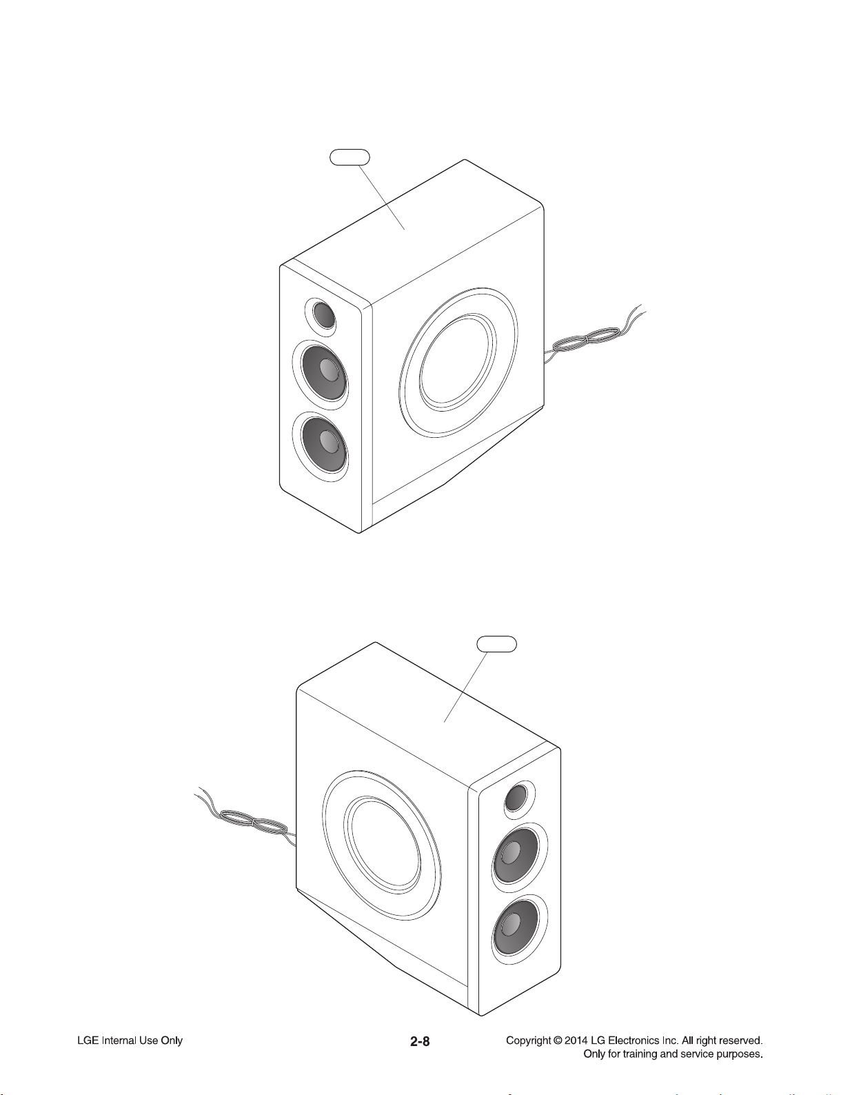
4. SPEAKER SECTION (CMS2730F)
A60R
A60L
Page 16

SECTION 3
ELECTRICAL
CONTENTS
ONE POINT REPAIR GUIDE ............................................................................................................................ 3-2
1. NO POWER PROBLEM ......................................................................................................................... 3-2
2. SPEAKER NO AUDIO OUTPUT ............................................................................................................ 3-3
3. USB NO DETECT ................................................................................................................................... 3-4
4. NO BOOTING ......................................................................................................................................... 3-5
ELECTRICAL TROUBLESHOOTING GUIDE ................................................................................................... 3-6
1. POWER (SMPS) ..................................................................................................................................... 3-6
2. P-SENS ................................................................................................................................................... 3-6
3. VKK CHECK ........................................................................................................................................... 3-6
4. μ-COM PART CHECK-1 ......................................................................................................................... 3-7
5. μ-COM PART CHECK-2 ......................................................................................................................... 3-7
6. FLD DISPLAY CHECK ........................................................................................................................... 3-8
7. TOUCH PART CHECK ........................................................................................................................... 3-9
8. PWM MODULATION CHECK ............................................................................................................... 3-10
9. POWER AMP PART CHECK ............................................................................................................... 3-11
10. VIDEO PART CHECK ........................................................................................................................... 3-12
11. TUNER FUNCTION CHECK ................................................................................................................. 3-13
DETAILS AND WAVEFORMS ON SYSTEM TEST AND DEBUGGING ....................................................... 3-14
1. SYSTEM 27 MHz CLOCK,RESET,FLASH R/W SIGNAL .................................................................... 3-14
2. SDRAM CLOCK .................................................................................................................................... 3-16
3. VIDEO PART (100% FULL COLOR-BAR) ........................................................................................... 3-16
4. HDMI PART .......................................................................................................................................... 3-17
WIRING DIAGRAM .......................................................................................................................................... 3-19
BLOCK DIAGRAM .......................................................................................................................................... 3-21
CIRCUIT DIAGRAMS ...................................................................................................................................... 3-23
1. SMPS CIRCUIT DIAGRAM .................................................................................................................. 3-23
2. MAIN - MICOM CIRCUIT DIAGRAM .................................................................................................... 3-25
3. MAIN - MPEG CIRCUIT DIAGRAM ...................................................................................................... 3-27
4. MAIN - RF SERVO CIRCUIT DIAGRAM .............................................................................................. 3-29
5. MAIN - I/O & ADC CIRCUIT DIAGRAM ............................................................................................... 3-31
6. MAIN - PWM & AMP CIRCUIT DIAGRAM ........................................................................................... 3-33
7. FRONT VFD CIRCUIT DIAGRAM ........................................................................................................ 3-35
8. FRONT JACK CIRCUIT DIAGRAM ...................................................................................................... 3-37
CIRCUIT VOLTAGE CHART ........................................................................................................................... 3-39
1. ICs ......................................................................................................................................................... 3-39
2. CONNECTORS ..................................................................................................................................... 3-41
3. CAPACITORS ....................................................................................................................................... 3-41
PRINTED CIRCUIT BOARD DIAGRAMS ....................................................................................................... 3-43
1. SMPS P.C.BOARD ............................................................................................................................... 3-43
2. MAIN P.C.BOARD ................................................................................................................................ 3-47
3. FRONT VFD P.C.BOARD ..................................................................................................................... 3-49
4. FRONT JACK P.C.BOARD ................................................................................................................... 3-51
3-1
Page 17

ONE POINT REPAIR GUIDE
1. NO POWER PROBLEM
No power problem occurs when you power on the unit.
1-1. Solution
Replace X100, IC101, IC103.
1-2. How to troubleshoot (Countermeasure)
1) Check X100 (Crystal).
If it does not oscillate, change X100.
2) Check IC103 (Reset IC).
IF its output voltage is not more than +2.7 V, change IC103.
3) Check IC101 (Micom).
After Power is ON if the pin63 of IC101 is not ‘High’, change IC101.
But, the new μ-com IC need to write program.
1-3. Service hint (Any picture / Remark)
IC101
X100
< MAIN board top view > < MAIN board bottom view >
IC103
3-2
Page 18

ONE POINT REPAIR GUIDE
2. SPEAKER NO AUDIO OUTPUT
No audio output problem occurs when you power on the unit.
2-1. Solution
Reassemble AMP IC heat-sink, replace IC700.
2-2. How to troubleshoot (Countermeasure)
1) Reassemble AMP IC heat-sink (heat-sink screw must be assembled tightly).
2) Still NG, please check IC700 Pin1, 2, 22(12 V), Pin29, 30, 31, 36, 37, 38 (26 V).
3) If it is not appear Vcc, change SMPS board assembly.
2-3. Service hint (Any picture / Remark)
< MAIN board top view >
3-3
IC700
Page 19

ONE POINT REPAIR GUIDE
3. USB NO DETECT
When USB insert, USB no detect on the unit.
3-1. Solution
Replace IC311.
3-2. How to troubleshoot (Countermeasure)
1) Please check IC311.
Pin3 : 5 V
2) If it is not OK, replace IC3A8.
3-3. Service hint (Any picture / Remark)
IC311
< FRONT JACK board top view >
3-4
Page 20

ONE POINT REPAIR GUIDE
4. NO BOOTING
When you turn on unit, it will display “Hello” or “Please wait” message continuously on front
panel, and it will not boot-up normally.
4-1. Solution
Replace X500.
4-2. How to troubleshoot (Countermeasure)
1) Please check the soldering status of 27 MHz crystal (X500).
2) Please check the frequency of 27 MHz crystal (X500).
3) If the crystal doesn’t oscillate, replace X500.
4) After changing it, if the set is still not booting, replace MAIN board assembly.
4-3. Service hint (Any picture / Remark)
X500
< MAIN board top view >
3-5
Page 21

ELECTRICAL TROUBLESHOOTING GUIDE
1. POWER (SMPS)
Power (AC cord in)
Check if PVDD
voltage of CN901 on Main BD
is 25~26 V.
YES
OK
2. P-SENS
μ-COM, P-SENS
Check R186
if DC V is over 3.3 V.
NO
Detach harness of CN901.
YES
Check if PVDD
voltage of CN901 on SMPS BD
is 25~26 V.
YES
Replace IC907.
NO
Check IC206 DC/DC circuit
and power circuit troubleshooting.
NO
Replace SMPS BD.
YES
OK
3. VKK CHECK
VKK check
Check IC205
Pin7 Vin(26V), CA202(-) DC V
is over -30 V.
YES
OK
NO
Check IC205 DC/DC circuit
and power circuit troubleshooting.
3-6
Page 22

ELECTRICAL TROUBLESHOOTING GUIDE
4. μ-COM PART CHECK-1
μ-com part check-1
Check
L206 3.7VA.
NO
YES
Check
both end voltage
of R186.
NO
YES
YES
OK OK
5. μ-COM PART CHECK-2
μ-com part check-2
Refer to
SMPS troubleshooting.
Check If
emitter voltage of Q103
is over 3.7 V.
YES
Check if Q103 of collector
voltage is over 2.7 V.
YES
NO
Check the periphery of Q103.
NO
Replace Q103.Check voltage of IC101 Pin4.
Check
L206 3.7 VA.
YES
Check
if output of D100,D101 is
3.3 V.
YES
Check If IC101_Pin14, 40, 55, 89
are 3.3 V.
YES
Check the operation.
X100: 12 MHz, X101: 32.768 kHz
YES
OK
NO
NO
Refer to
SMPS troubleshooting.
Replace D100, D101.
3-7
Page 23

ELECTRICAL TROUBLESHOOTING GUIDE
6. FLD DISPLAY CHECK
FLD display check
Check
IC205 Pin7(26 V)
voltage.
YES
Check if both end voltage of
FL+, FL- are -24V, -28V
VKK : -31V.
YES
Check IC301
Pin9 (3.3 V)
Pin50 VKK (-31 V).
YES
NO
NO
Refer to
SMPS troubleshooting.
Check CN301 connection.
YES
Check each
Pin voltage.
YES
OK
If voltage is not 3.3 V,
check input and output of D301.
YES
NO
Check FFC cable.
Check
data communication
IC101-->IC301
Pin27-->Pin3 STB,
Pin26-->Pin2 DATA,
Pin28-->Pin1 CLK
NO
YES
YES
OK OK
Check IC301.
YES
OK
Check DATA input
IC101: Pin26, 27, 28.
YES
Check DATA output
IC101: Pin26.
YES
Check IC101.
YES
NO
NO
Replace IC301.
Replace IC101.FLD light on?
3-8
Page 24

ELECTRICAL TROUBLESHOOTING GUIDE
7. TOUCH PART CHECK
Touch part check
IC303 Pin1
voltage 3.3 V OK?
YES
Check TOUCH_IRQ signal(IC303 Pin6)
When you touch pad, it is ‘Low’.
When you non-touch pad, it’s ‘High’.
YES
TOUCH_DAT,
CLK signal OK?
YES
OK
NO
NO
NO
Check the FFC cable.
Replace IC303.
Check the connection,
or replace IC101.
3-9
Page 25

ELECTRICAL TROUBLESHOOTING GUIDE
8. PWM MODULATION CHECK
PWM modulation
part check
IC602 Pin9, 14, 35, 50
Check
3.3 V.
YES
Check
X600 12.288 MHz
operation.
YES
IC602
Pin16: PWM RESET
Pin20: PWM SDA
Pin21: PWM SCL
YES
IC602(TAS5548) data input
Pin22,23,24(LRCK,BCK,
Check
DATA)
NO
NO
NO
NO
IC203 DC/DC circuit
and replace IC602.
Replace X600.
Check
line resistor output
SDA: R610, SCL: R611,
RST: R616..
YES
OK
Check
IC500 DVD MPEG
I2S output.
NO
NO
Replace related resistor.
Replace IC500.
YES
Check
PWM 46, 47, 48, 49 (SPK)
PWM 1, 2, 3, 4 (HP).
YES
OK
NO
YES
OK
Check IC602
HP SEL: Pin17
MUTE: Pin19.
YES
OK
3-10
NO
Replace IC602.
Page 26

ELECTRICAL TROUBLESHOOTING GUIDE
9. POWER AMP PART CHECK
Power AMP part check
CN901
Pin1, 2, 3: 26 V.
YES
Check each IC700
Pin29, 30, 31, 36, 37, 38 voltage.
YES
Check
IC700 Pin1, 2, 22: +12 V
input.
YES
Check PWM modulator input
each Pin5, 6, 14, 15.
YES
Power IC700
Pin27, 28, 32, 35, 39, 40 output.
YES
Check output line coil.
NO
NO
NO
Refer to SMPS troubleshooting.
Check each line resistor output voltage.
Replace the coil.
OK
YES
3-11
Page 27

ELECTRICAL TROUBLESHOOTING GUIDE
10. VIDEO PART CHECK
Video part check
pin of D502 are short with each
Check each
other?
NO
JK501 Pin3
video signal OK?
YES
Check external
cable OK?
YES
If it’s still NG,
check display device(TV or monitor).
YES
OK
YES
NO
NO
Check or replace D502.
Check or replace
L501, C567, C568, R599.
Replace the cable.
3-12
Page 28

ELECTRICAL TROUBLESHOOTING GUIDE
11. TUNER FUNCTION CHECK
Tuner function check
tuner module(TU100)
Check
operation.
YES NO
Check IC201(CS5346) Pin41,42,43,44
output waveform.
YES
Waveform OK?
YES
Check IC500
Pin48, 49, 50, 51 I2S signal.
YES
OK?
YES
NO
NO
NO
Check tuner module voltage
(Pin6 : +3.3 V).
Replace the module.
Check or replace IC201, IC207.
Replace IC500.
Refer to PWM part.
3-13
Page 29

DETAILS AND WAVEFORMS ON SYSTEM TEST AND DEBUGGING
1
3
2
1. SYSTEM 27 MHz CLOCK,RESET,FLASH R/W SIGNAL
1)
MT1389FE/GH
2)
MT1389FE/GH
main clock is at 27 MHz(X500)
IC500
1
FIG 1-1
reset is high active.
DVD_RESET
3.3 V
2
1.2 V
3
4
IC500
FIG 1-2
IC500
4
3-14
Page 30

3) Flash R/W enable signal during download(Downloading)
5
6
SF_DI
SF_DO
5
6
FIG 1-3
3-15
Page 31

8
2. SDRAM CLOCK
7
1)
MT1389FE/GH
DCLK = 93MHz, Vp-p=2.2, Vmax=2.7V
SDCLK
main clock is at 27 MHz(X500)
7
IC502
FIG 2-1
3. VIDEO PART (100% FULL COLOR-BAR)
8
CVBS
3-16
Page 32

4. HDMI PART
HDMI_SDA
9
11
10
HDMI_SCL
12
HDMI_CLK HDMI_DATA
3-17
9
10
11
12
Page 33

3-18
Page 34

3-19 3-20
FRONT VFD
(FR-4 EPOXY 2LAYER)
LOADER
MAIN
(FR-4 EPOXY 2LAYER)
SMPS
CN100 CN107 CN102
FAN
FRONT JACK
(FR-4 EPOXY
2LAYER)
CN201CN101
CN401CN400
BT
DAB
CN101
CN202
Harness
9P
Harness
15P
FFC
15P
FFC
12P
Harness
6P
FFC
9P
FFC
23P
WIRING DIAGRAM
Page 35

3-21 3-22
TAS5612L
S56
SANYO
(100PIN)
SDRAM
(16MB)
FLASH
(4MByte)
DB[0-15]
DMA[0-10]
12 MHz
D+, D-
TUNER L/R
PORT L/R
USB
CVBS OUT
DVD_RESET
DVD_TX
DVD_RESET
DVD_RX
TUNER(FM)
PORTABLE
COMPOSITE
MTK1389GH
(176PIN)
27 MHz
ADC
(CS5346)
3.3/5V
CVBS
FO CUS/SLED
SPINDLE/TRACKING
F+/-, T+/-
SLED+/SPINDLE+/-
MD_DVD, MD_CD
LD_DVD, LD_CD
VR_DVD, VR_CD
A, B, C, D, E, F, RF
MD
OPU
Motor IC
(AM5890)
3.3/1.2V
HDMI OUT
TMDS
CEC_TX/RX
4CH,5V
3.3V
3.3V
SPI
I2C
5346_DATA
I2C,RESET
MCK,LRCK
BCK
1080P
5V
EEPROM
(2KByte)
I2C
32.768kHz
LC87F5NC8A
3.3V
3.3V
EEPROM
(2KByte)
3.3V 3.3V
LPF
AMP
3.3V
I2C
MCLK,LRCK, BCK,DATA
VFD Driver
MC3501
IR
TOUCH KEY * 10 EA
SPI
Touch
TC390
I2C
3.3V,Vkk
FL+,FL-
Key
3.3V
TPA6132A2
3.3V
FUNCTION KEY * 4 EA
PVDD(26V)
PWM
TAS5548
BT_SPDIF_IN
OPTIAL IN
CTRL
BT M/M
MODULE
LED * 11 EA
UART
3.3V
DAB L/R
DAB
LOAD+/-
OPEN/CLOSE
1CH,9.5V
CS8422
Motor IC
(DRV8837)
I2C
MCLK
BCK
LRCK
A_DATA
12V
FAN_CTRL
option
24.576MHz
BLOCK DIAGRAM
Page 36

3-23 3-24
A
1
2
3
4
5
6
7
8
9
10
11
12
B C D E F G H I J K L M N O P Q R ST
SMPS
EAX65707301_5.1.2_SMPS
2014. 03. 26
Warning
Parts that are shaded are critical with
respect to risk of fire or electrical shock.
CAUTION:
Danger if fuse is incorrectly replaced.
Replace only with the type identical to fuse rating
and(or) model name described in main label.
CIRCUIT DIAGRAMS
1. SMPS CIRCUIT DIAGRAM
WHEN SERVICING THIS CHASSIS, UNDER NO
CIRCUMSTANCES SHOULD THE ORIGINAL DESIGN
BE MODIFIED OR ALTERED WITHOUT PERMISSION
FROM THE LG CORPORATION. ALL COMPONENTS
SHOULD BE REPLACED ONLY WITH TYPES
IDENTICAL TO THOSE IN THE ORIGINAL CIRCUIT.
SPECIAL COMPONENTS ARE SHADED ON THE
SCHEMATIC FOR EASY IDENTIFICATION. THIS
CIRCUIT DIAGRAM MAY OCCASIONALLY DIFFER
FROM THE ACTUAL CIRCUIT USED. THIS WAY,
IMPLEMENTATION OF THE LATEST SAFETY AND
PERFORMANCE IMPROVEMENT CHANGES INTO
THE SET IS NOT DELAYED UNTIL THE NEW
SERVICE LITERATURE IS PRINTED.
1. Shaded( ) parts are critical for safety. Replace only
with specified part number.
2. Voltages are DC-measured with a digital voltmeter
during Play mode.
IMPORTANT SAFETY
NOTE :
Page 37

3-25 3-26
A
1
2
3
4
5
6
7
8
9
10
11
12
B C D E F G H I J K L M N O P Q R ST
MICOM
EAX65726401_6.1.2_MAIN_SD
2014. 03. 28
2. MAIN - MICOM CIRCUIT DIAGRAM
Page 38

3-27 3-28
8
1
4
3
2
9
10
11
12
7
5
6
: WAVEFORM NUMBER
A
1
2
3
4
5
6
7
8
9
10
11
12
B C D E F G H I J K L M N O P Q R ST
MPEG
EAX65726401_6.1.2_MAIN_SD
2014. 03. 28
3. MAIN - MPEG CIRCUIT DIAGRAM
Page 39

3-29 3-30
A
1
2
3
4
5
6
7
8
9
10
11
12
B C D E F G H I J K L M N O P Q R ST
RF SERVO
EAX65726401_6.1.2_MAIN_SD
2014. 03. 28
4. MAIN - RF SERVO CIRCUIT DIAGRAM
Page 40

3-31 3-32
A
1
2
3
4
5
6
7
8
9
10
11
12
B C D E F G H I J K L M N O P Q R ST
I/O & ADC
EAX65726401_6.1.2_MAIN_SD
2014. 03. 28
5. MAIN - I/O & ADC CIRCUIT DIAGRAM
Page 41

3-33 3-34
A
1
2
3
4
5
6
7
8
9
10
11
12
B C D E F G H I J K L M N O P Q R ST
PWM & AMP
EAX65726401_6.1.2_MAIN_SD
2014. 03. 28
6. MAIN - PWM & AMP CIRCUIT DIAGRAM
Page 42

3-35 3-36
A
1
2
3
4
5
6
7
8
9
10
11
12
B C D E F G H I J K L M N O P Q R ST
FRONT VFD
EAX65726601_10.1.3_VFD_SD
2014. 03. 26
7. FRONT VFD CIRCUIT DIAGRAM
Page 43

3-37 3-38
A
1
2
3
4
5
6
7
8
9
10
11
12
B C D E F G H I J K L M N O P Q R ST
FRONT JACK
EAX65726701_10.1.3_JACK_SD
2014. 03. 26
8. FRONT JACK CIRCUIT DIAGRAM
Page 44

3-39 3-40
CIRCUIT VOLTAGE CHART
1. ICs
LOCATION NAME SPEC CLASSIFICATION PIN NUMBER SPEC ENG. VOLTAGE REAL VOLTAGE
MAIN BOARD
IC101 IC,Microcontrollers LC87F5WC8A
3.3VA 14 PIN
2.2 ~ 5.5
3.30 3.42
3V3MICOM 40,55,89 PIN 3.30 3.48
IC102 IC,EEPROM M24C16 3V3MICOM 8PIN 1.8 ~ 3.6 3.30 3.48
IC103 IC,Voltage Detector AZ7027RTRE1 3.7VA 1 PIN 0 ~ 18 3.50 3.58
IC201 IC,A/D Converter CS5346-CQZR
DVCC_3.3V 46PIN 3.13 ~ 3.47 3.30 3.24
AVCC_5V 14PIN 4.75 ~ 5.25 5.00 5.12
IC203
IC,DC,DC Converter MP1432 -0.3V to 48V 0.8V to 42V 2.5W SOIC T/REEL 8P MSL 2
VCC_12V 7 PIN 4.5~45 12.00 12.00
VOUT(3.3V) VOUT 0.8~42 3.30 3.31
IC204
VCC_12V 7 PIN 4.5~45 12.00 12.00
VOUT(5.6V) VOUT 0.8~42 5.60 5.60
IC206
26VA 7 PIN 4.5~45 26.00 24.77
VOUT(3.7V) VOUT 0.8~42 3.70 3.74
IC205
26VA 7 PIN 4.5~45 26.00 24.76
VOUT VOUT 0.8~42 12.00 12.07
IC207 IC,I/O Support Chip CS8422-CNZR DVCC 3.3V 3,19,22 PIN 3.135 ~ 3.465 3.30 3.24
IC208 IC,LDO Voltage Regulator LM37102D
5.6V 2PIN
2.25 ~ 16
5.60 5.57
VOUT(5V) 3 PIN 5.10 5.12
IC400 IC,Motor Driver AM5890 5ch dvd-p 4.3to13.2v 9v 1.7W HSOP R/TP 28P DVCC 5V 8,19 PIN 4.3 ~ 13.2 5.00 5.16
IC401
IC,Motor Driver
DRV8837 -0.3 ~ 7 0 0W WSON T/REEL 8P 1
VCC9.5 1 PIN 0~11 9.50 9.77
DVCC_3.3V 8 PIN 1.8~7 3.30 3.30
IC403 IC,Voltage Regulator AZ1117BH-ADJTRE1 15V ADJ 0W SOT223 R/TP 3P - BCD
VCC_12V 3 PIN 15.00 12.00 11.76
VCC9.5 2 PIN 15.00 9.50 9.50
IC500 IC,Video Processors MT1389FE/GH
DVCC 3.3V
2,12,22,38,57,67,101,134,135,14
0,142,151,152,163,164,
3.1 ~ 3.6 3.30 3.18
VCC 1.2V 1,25,79,109,165 1.1 ~ 1.3 1.20 1.22
IC501 IC,EEPROM M24C16 DVCC_3.3V 8 PIN 1.8 ~ 3.6 3.30 3.25
IC502 IC,SDRAM W9812G6JH-6 128MBIT DVCC 3.3V 1,3,9,14,27,43,49 3.0 ~ 3.6 3.30 3.24
IC602 PWM TAS5548 AVCC_3.3V 14,35,50 PIN 3 ~ 3.6 3.30 3.26
IC700 IC,Audio Amplifi er TAS5612LA 125-W Class-D
VCC_12V 2 PIN 10.8 ~ 13.2 12.00 11.65
GVDD 1,22 PIN 10.8 ~ 13.2 12.00 11.65
PVDD 36,37,38,29,30,31 PIN 12 ~ 34 26.00 25.60
IC701 IC,Audio Amplifi er TPA6132A2 AVCC_3.3V 14 PIN 2.3 ~ 5.5 3.30 3.27
FRONT JACK BOARD
IC311 IC,LDO Voltage Regulator TJ3966
VIN 1 PIN 0~7V 5.60 5.600
VOUT 3 PIN 5V 5.06 5.000
FRONT VFD BOARD
IC301 IC,Display Driver MC3501 3.3VA 9 PIN 2.7~5.5 3.30 3.370
RC301 Receiver Module R24FH7H 3.3VA 1 PIN 2.7~5.5V 3.3V 3.300
TOUCH BOARD
IC301 IC,Capacitive Touch Sensor TOUCHCORE390 8-BIT 3.3VA 1 PIN 2.7~3.6 3.30 3.360
Page 45

3-41 3-42
2. CONNECTORS
3. CAPACITORS
LOCATION PIN NUMBER SPEC REAL VOLTAGE LOCATION PIN NUMBER SPEC REAL VOLTAGE
MAIN
Ù
SMPS
CN202
1,2,3 PVDD 25.4
CN901
1,2,3 PVDD 25.4
4,5,6 DGND 0 4,5,6 DGND 0
MAIN
Ù
TOP JACK
CN107
(TOP JCAK)
4,9,10,12 DGND 0
CN370
4,9,10,12 GND 0
11 USB_5.6V 5.6 11 VCC_5V 5.6
MAIN
Ù
VFD
CN102
(VFD)
3,7,14 DGND 0
CN301
1,2 3.7V 3.68
6 FL+ -26.2 4 VKK -28.9
5 FL- -21.9 5 FL- -21.9
4 VKK -28.9 6 FL+ -26.2
1,2 3.7VA 3.68 3,7 GND 0
MAIN
Ù
B/T
CN100 (B/T)
5.6 DVDD_3V3 3.27
1,11 DGND 0
LOCATION SPEC ENG. VOLTAGE REAL VOLTAGE
MAIN BOARD
C136 1000uF/6.3V 3.3 3.42
C137 220uF/16V 12 11.75
C283 10uF/16V 3.3 3.24
C284 10uF/16V 3.3 2.43
C298 10uF/16V 3.3 3.23
C404 220uF/16V 5 5.10
C489 100uF/16V 1.2 1.25
C701 470uF/50V 26 25.40
C732 470uF/50V 26 25.40
C902 4.7uF/50V 26 25.40
C907 4.7uF/50V 26 25.40
C910 1000uF/6.3V 4.5 4.88
C912 47uF/50V 22 21.90
C913 47uF/50V 30 29.20
C914 47uF/50V 27 26.30
C942 4.7uF/50V 26 25.40
C952 4.7uF/50V 26 25.40
C956 4.7uF/50V 26 25.40
LOCATION SPEC ENG. VOLTAGE REAL VOLTAGE
FRONT JACK BOARD
C377 10uF/16V 5.6 5.50
C3A4 10uF/16V 5.6 5.50
FRONT VFD BOARD
C346 100uF/16V 3.3 3.37
C349 47uF/50V 90 28.9
C350 47uF/50V 22 21.9
C353 47uF/50V 27 26.3
C354 47uF/16V 3.3 3.29
MIC BOARD
C3M4 22uF/16V 2 2
Page 46

3-43 3-44
PRINTED CIRCUIT BOARD DIAGRAMS
1. SMPS P.C.BOARD
(TOP VIEW)
Page 47

3-45 3-46
SMPS P.C.BOARD
(BOTTOM VIEW)
NOTE) Warning
Parts that are critical with respect to risk
of fire or electrical shock.
Page 48

3-47 3-48
2. MAIN P.C.BOARD
(TOP VIEW) (BOTTOM VIEW)
Page 49

3-49 3-50
3. FRONT VFD P.C.BOARD
(TOP VIEW) (BOTTOM VIEW)
Page 50

3-51 3-52
4. FRONT JACK P.C.BOARD
(TOP VIEW) (BOTTOM VIEW)
Page 51

3-53 3-54
 Loading...