

Page 1
Features of CX8700
1. Wave Type
CELLULAR : G7W
•
• PCS : G7W
2. Frequency Scope
Transmit Frequency (MHz)
Receive Frequency (MHz)
CELLULAR
824.82 ~ 848.19 1850~1910 869.82~893.19 1930~1990 1575.42
3. Rated Output Power :
PCS = 0.20W
4. Output Conversion Method :
5. Voltage and Current Value of Termination Part Amplifier (Catalogue included)
MODE Part Name Voltage Current Power
CELLULAR AWT6310R 4.2V 600mA 0.20W
PCS AWT6310R 4.2V 600mA 0.20W
PCS
CELLULAR = 0.20W
This is possible by correcting the key board channel.
CELLULAR
PCS
6. Functions of Major Semi-Conductors
Classification Function
MSM6550 Terminal operation control and digital signal processing
GPS
Memory MCP
(HYI0UGG0MF1P-6SS0E)
RFR6500 Converts Rx RF signal to baseband signal
RFT6150 Converts baseband signal to Tx RF signal
7. Frequency Stability
• CELLULAR : ±0.5PPM
PCS : ±0.1PPM
•
LG Electronics Inc.
Z3X-BOX.COM
Flash Memory (1Mbit) + SDRAM (512Mbit)
Storing of terminal operation program
Page 2

CX8700
CDMA Mobile Subscriber Unit
CX8700
SERVICE MANUAL
TRI BAND CDMA
[PCS/Cellular/GPS]
CDMA MOBILE PHONE
Z3X-BOX.COM
LG Electronics Inc.
- 2 -
Page 3

CX8700
Table of Contents
General Introduction
........................................................................................................................................ 4
CHAPTER 1. System Introduction
1. System Introduction......................................................................................................................5
2. Features and Advantages of CDMA Mobile Phone .................................................................6
3. Specification...................................................................................................................................9
4. Installation ..................................................................................................................... 14
CHPATER 2. NAM Input Method
1. NAM Program Method and Telephone Number Inputting Method .................................16
CHAPTER 3. Circuit Description
1. RF Transmit/Receive Part..........................................................................................................26
2. Digital/Voice Processing Part.....................................................................................................33
CHAPTER 4. Trouble Shooting……………………………………………….…………………….37
CHAPTER 5. Safety……………………………………………………………….……………..…..88
CHAPTER 6. Glossary………………………………………………………….………………..…..91
APPENDIX……………………………………………………………………………………….….103
Z3X-BOX.COM
LG Electronics Inc.
- 3 -
Page 4
CX8700
General Introduction
The CX8700 phone has been designed to operate on the latest digital mobile communication technology, Code
Division Multiple Access (CDMA). This CDMA digital technology has greatly enhanced voice clarity and can
provide a variety of advanced features. Currently, CDMA mobile communication technology has been
commercially used in Cellular and Personal Communication Service (PCS). The difference between them is the
operating frequency spectrum. Cellular uses 800MHz and PCS uses 1.9GHz. The CX8700 support GPS Mode,
we usually call it tri-band phone. Also, CX8700 works on Advanced Mobile Phone Service (S-GPS). We call it
dual-mode phone. If one of the Cellular, PCS base stations is located nearby, Call fail rate of triple-mode phone
is less than dual-mode phone or single-mode phone.
The CDMA technology adopts DSSS (Direct Sequence Spread Spectrum). This feature of DSSS enables the
phone to keep communication from being crossed and to use one frequency channel by multiple users in the
same specific area, resulting that it increases the capacity 10 times more compared with that in the analog mode
currently used. Soft/Softer Handoff, Hard Handoff, and Dynamic RF power Control technologies are combined
into this phone to reduce the call being interrupted in a middle of talking over the phone.
Cellular and PCS CDMA network consists of MSO (Mobile Switching Office), BSC (Base Station Controller),
BTS (Base station Transmission System), and MS (Mobile Station). The following table lists some major
CDMA Standards.
CDMA Standard Designator Description
Basic air interface TIA/EIA/IS-95-A/B/C
ANSI J-STD-008
Network TIA/EIA/IS-634
TIA/EIA/IS/651
TIA/EIA/IS-41-C
TIA/EIA/IS-124
Service TIA/EIA/IS-96-B
Z3X-BOX.COM
TIA/EIA/IS-99
TIA/EIA/IS-637
TIA/EIA/IS-657
Protocol between MS and BTS for Cellular & AMPS
Protocol between MS and BTS for PCS
MAS-BS
PCSC-RS
Intersystem operations
Nom-signaling data comm.
Speech CODEC
Assign data and fax
Short message service
Packet data
Performance TIA/EIA/IS-97
TIA/EIA/IS-98
ANSI J-STD-018
ANSI J-STD-019
TIA/EIA/IS-125
* TSB –74: Protocol between an IS-95A system and ANSI J-STD-008
LG Electronics Inc.
Cellular base station
Cellular mobile station
PCS personal station
PCS base station
Speech CODEC
- 4 -
Page 5

CX8700
Chapter1. System Introduction
1.1 CDMA Abstract
The CDMA mobile communication system has a channel hand-off function that is used for collecting the
information on the locations and movements of mobile telephones from the cell site by automatically controlling
several cell site through the setup of data transmission routes, and then enabling one switching system to carry
out the automatic remote adjustment. This is to maintain continuously the call state through the automatic
location confirmation and automatic radio channel conversion when the busy subscriber moves from the service
area of one cell site to that of another by using automatic location confirmation and automatic radio channel
conversion functions. The call state can be maintained continuously by the information exchange between
switching systems when the busy subscriber moves from one Cellular system area to the other Cellular system
area.
In the Cellular system, the cell site is a small-sized low output type and utilizes a frequency allocation system
that considers mutual interference, in an effort to enable the re-use of corresponding frequency from a cell site
separated more than a certain distance.
Unlike the time division multiple access (TDMA) or frequency division multiple access (FDMA) used in the
band limited environment, the Code Division Multiple Access (CDMA) system which is one of digital Cellular
systems is a multi-access technology under the interference limited environment. It can process more number of
subscribers compared to other systems (TDMA system has the processing capacity three times greater than the
existing FDMA system whereas CDMA system, about 12~15 times of that of the existing system).
CDMA system can be explained as follows; TDMA or CDMA can be used to enable each person to talk
alternately or provide a separate room for each person when two persons desire to talk with each other at the
same time, whereas FDMA can be used to enable one person to talk in soprano, whereas the other in bass (one
of the two talkers can carry out synchronization for hearing in case there is a bandpass filter function in the area
of the hearer). Another available method is to make two persons to sing in different languages at the same time,
space, and frequency when wishing to let the audience hear the singing without being confused. This is the
characteristic of CDMA.
On the other hand, when employing the CDMA technology, each signal has a different pseudo-random binary
sequence used to spread the spectrum of carrier. A great number of CDMA signals share the same frequency
spectrum. In the perspective of frequency area or time area, several CDMA signals are overlapped. Among these
types of signals, only desired signal energy is selected and received through the use of pre-determined binary
sequence; desired signals can be separated, and then received with the correlator used for recovering the
spectrum into its original state. At this time, the spectrums of other signals that have different codes are not
recovered into its original state, and appears as the self-interference of the system.
Z3X-BOX.COM
LG Electronics Inc.
- 5 -
Page 6

CX8700
2. Features and Advantages of CDMA Mobile Phone
2.1 Various Types of Diversities
When employing the narrow band modulation (30kHz band) that is the same as the analog FM modulation
system used in the existing Cellular system, the multi-paths of radio waves create a serious fading. However, in
the CDMA broadband modulation (1.25MHz band), three types of diversities (time, frequency, and space) are
used to reduce serious fading problems generated from radio channels in order to obtain hig h-quality calls.
Time diversity can be obtained through the use of code interleaving and error correction code whereas frequency
diversity can be obtained by spreading signal energy to wider frequency band. The fading related to normal
frequency can affect the normal 200~300KHz among signal bands and accordingly, serious effect can be
avoided. Moreover, space diversity (also called path diversity) can be realized with the following three types of
methods.
First, it can be obtained by the duplication of cell site receive antenna. Second, it can be obtained through the
use of multi-signal processing device that receives a transmit signal having each different transmission delay
time and then, combines them. Third, it can be obtained through the multiple cell site connection (Soft Handoff)
that connects the mobile station with more than two cell sites at the same time.
2.2 Power Control
The CDMA system utilizes the forward (from a base station to mobile stations) and backward (from the mobile
station to the base station) power control in ord er to in crease the call p ro cessing capacity an d ob tain h igh -q uality
calls. In case the originating signals of mobile stations are received by the cell site in the minimum call quality
level (signal to interference) through the use of transmit power control on all the mobile stations, the system
capacity can be maximized.If the signal power of mobile station is received too strong, the performance of that
mobile station is improved. However, because of this, the interference on other mobile stations using the same
channel is increased and accordingly, the call quality of other subscribers is reduced unless the maximum
accommodation capacity is reduced.
In the CDMA system, forward power control, backward open loop power control, and closed loop power control
methods are used. The forward power control is carried out in the cell site to reduce the transmit power on
mobile stations less affected by the multi-path fading and shadow phenomenon and the interference of other cell
sites when the mobile station is not engaged in the call or is relatively nearer to the corresponding cell site. This
is also used to provide additional power to mobile stations having high call error rates, located in bad reception
areas or far away from the cell site.
The backward open loop power control is carried out in a corresponding mobile station; the mobile station
measures power received from the cell site and then, reversely increases/decreases transmit power in order to
compensate channel changes caused by the forward link path loss and terrain characteristics in relation to the
mobile station in the cell site. By doing so, all the mobile transmit signals received by the base station have same
strength.
Moreover, the backward closed loop power control used by the mobile station is performed to control power
using the commands issued out by the cell site. The cell site receives the signal of each corresponding mobile
station and compares this with the pre-set threshold value and then, issues out power increase/decrease
commands to the corresponding mobile station every 1.25msec (800 times per second). By doing so, the gain
tolerance and the different radio propagation loss on the forward/backward link are complemented.
Z3X-BOX.COM
LG Electronics Inc.
- 6 -
Page 7

CX8700
2.3 Voice Encoder and Variable Data Speed
The bi-directional voice service having variable data speed provides voice communication which employs
voice encoder algorithm having power variable data rate between the base station and the mobile station. On the
other hand, the transmit voice encoder performs voice sampling and then, creates encoded voice packets to be
sent out to the receive voice encoder, whereas the receive voice encoder demodulates the received voice packets
into voice samples.
One of the two voice encoders described in the above is selected for use depending on inputted automatic
conditions and message/data; both of them utilize four-stage frames of 9600, 4800, 2400, and 1200 bits per
second for Cellular and 14400,7200,3600,1800 bits per second for PCS, so PCS provide relatively better voice
quality (almost twice better than the existing celluar system). In addition, this type of variab le voice encoder
utilizes adaptive threshold values on selecting required data rate. It is adjusted in accordance with the size of
background noise and the data rate is increased to high rate only when the voice of caller is inputted.
Therefore, background noise is suppressed and high-quality voice transmission is possible under the
environment experiencing serious noise. In addition, in case the caller does not talk, data transmission rate is
reduced so that the transmission is carried out in low energy. This will reduce the interference on other CDMA
signals and as a result, improve system performance (capacity increased by about two times).
2.4 Protecting Call Confidentiality
Voice privercy is provided in the CDMA system by means of the private long code mask used for PN spreading.
Voice privacy can ve applied on the traffic channels only. All calls are initiated using the public long code mask
for PN spreading. The mobile station user may request voice privacy during call setup using the origination
message or page response message, and during traffic channel operation using the long code transition request
order.
The Transition to private long code mask will not be performed if authentication is not performed. To initiate a
transition to the private or public long code mask, either the base station or the mobile station sends a long code
transition request order on the traffic channel.
2.5 Soft Handoff
A handoff in which the mobile station commences communications with a new base station without interrupting
communications with the old base station. Soft handoff can only be used between CDMA channels having
identical freqeuncy assignments.
Z3X-BOX.COM
2.6 Frequency Re-Use and Sector Segmentation
Unlike the existing analog Cellular system, the CDMA system can reuse the same frequency at the adjacent cell.
there is no need to prepare a separate frequency plan. Total interference generated on mobile station signals
received from the cell site is the sum of interference generated from other mobile stations in the same cell site
and interference generated from the mobile station of adjacent cell site. That is, each mobile station signal
LG Electronics Inc.
- 7 -
Page 8

CX8700
generates interference in relation to the signals of all the other mobile stations .
Total interference from all the adjacent cell sites is the ratio of interference from all the cell sites versus total
interference from other mobile stations in the same cell site (about 65%). In the case of directional cell site, one
cell normally uses a 120°sector antenna in order to divide the sector into three. In this case, each antenna is
used only for 1/3 of mobile stations in the cell site and accordingly, interference is reduced by 1/3 on the average
and the capacity that can be supported by the entire system is increased by three times.
2.7 Soft Capacity
The subscriber capacity of the CDMA system is flexible depending on the relation between the number of
users and service classes. For example, the system operator can increase the number of channels available for
use during the busy hour despite the drop in call quality. This type of function requires 40% of normal call
channels in the standby mode during the handoff, in an effort to avoid call disconnection resulting from the lack
of channels.
In addition, in the CDMA system, services and service charges are classified further into different classes so that
more transmit power can be allocated to high class service users for easier call set-up; they can also be given
higher priority of using hand-off function than the general users.
Z3X-BOX.COM
LG Electronics Inc.
- 8 -
Page 9
CX8700
3. Specification
3.1 General Specification
3.1.1 Transmit/Receive Frequency Interval :
1) CELLULAR : 45 MHz
2)
PCS : 80 MHz
3.1.2 Number of Channels (Channel Bandwidth)
1) CELLULAR : 20 Channels
2) PCS : 48 Channels
3.1.3 Operating Voltage : DC 3.3~4.2V
3.1.4 Battery Power Consumption : DC 3.7V
SLEEP IDLE MAX POWER
CELLULAR
PCS
1 mA 110~140mA 700 mA (24 dBm)
1 mA 120~150 mA 700 mA (24 dBm)
3.1.5 Operating Temperature : -20°C ~ +60°C
3.1.6 Frequency Stability
1) CDMA : ±0.5PPM
2) PCS : ±0.1PPM
3.1.7 Antenna : Intenna Type, 50 Ω
3.1.8 Size and Weight
1) Size : 97(H) * 49.5(W) * 13.6(D) mm
2) Weight : 110 g (Approximately with standard battery)
3.1.9 Channel Spacing
1) CELLULAR : 1.25MHz
2) PCS: 1.25 MHz
3.1.10 Battery Type, Capacity and Operating Time.
Z3X-BOX.COM
Unit = Hours : Minutes
Standard (1,100mAh)
Standby Time
Talk time
LG Electronics Inc.
CELLULAR About 380 Hours (SCI=2)
PCS About 380 Hours (SCI=2)
CELLULAR 230 Minutes (-92dBm input)
PCS 230 Minutes (-92dBm input)
- 9 -
Page 10

CX8700
3.2 Receive Specification
3.2.1 Frequency Range
1) CELLULAR : 869.820 MHz ~ 893.190 MHz
2) PCS : 1930 MHz ~ 1990 MHz
3) GPS : 1575.42 MHz
3.2.2 Local Oscillating Frequency Range :
1) CELLULAR : 1738.08MHz ~ 1787.94MHz
2) PCS : 1715.56MHz ∼ 1768.89MHz
3) GPS : 3150.84MHz
3.2.3 Sensitivity
1) CELLULAR : -104dBm (C/N 12dB or more)
2) PCS : -104dBm (C/N 12dB or more)
3) GPS : -148.5dBm (without SA mode)
3.2.4 Selectivity
1) CELLULAR : 3dB C/N Degration (With Fch±1.25 kHz : -30dBm)
2) PCS : 3dB C/N Degration (With Fch±1.25 kHz : -30dBm)
3.2.5 Spurious Wave Suppression : Maximum of -80dB
3.2.6 CDMA Input Signal Range
z Dynamic area of more than -104~ -25 dB: 79dB at the 1.23MHz band.
3.3 Transmit Specification
3.3.1 Frequency Range
1) CELLULAR : 824.820MHz ~ 848.190MHz
2) PCS : 1850 MHz ~ 1910 MHz
3.3.2 Output Power
Z3X-BOX.COM
1) CELLULAR : 0.224W
2) PCS: 0.224W
3.3.3 Interference Rejection
1) Single Tone : -30dBm at 900 kHz (CELLULAR), -30dBm at 1.25MHz(PCS)
2) Two Tone : -43dBm at 900 kHz & 1700kHz(CELLULAR), -43dBm at 1.25 MHz & 2.05 MHz
(PCS)
LG Electronics Inc.
- 10 -
Page 11
CX8700
3.3.11 CDMA TX Frequency Deviation :
1) CELLULAR: +300Hz or less
2) PCS: ± 150Hz
3.3.12 CDMA TX Conducted Spurious Emissions
1) CELLULAR : 900kHz : - 42 dBc/30kHz below
1.98MHz : - 54 dBc/30kHz below
2) P C S : 1.25MHz : - 42 dBc/30kHz below
1.98MHz : - 50 dBc/30kHz below
3.3.13 CDMA Minimum TX Power Control
1) CELLULAR : - 50dBm below
2) P C S : -50dBm below
3.4
MS (Mobile Station) Transmitter Frequency
3.4.1 CELLULAR mode
Ch # Center Freq. (MHz) Ch # Center Freq. (MHz)
1011
29
70
111
152
193
234
275
316
363
Z3X-BOX.COM
824.640
825.870
827.100
828.330
829.560
830.790
832.020
833.250
834.480
835.890
404
445
486
527
568
609
650
697
738
779
837.120
838.350
839.580
840.810
842.040
843.270
844.500
845.910
847.140
848.370
3.4.2 PCS mode
Ch # Center Freq (MHz) Ch # Center Freq (MHz) Ch # Center Freq (MHz)
25 1851.25 425 1871.25 825 1891.25
50 1852.50 450 1872.50 850 1892.50
75 1853.75 475 1873.75 875 1893.75
100 1855.00 500 1875.00 900 1895.00
125 1856.25 525 1876.25 925 1896.25
150 1857.50 550 1877.50 950 1897.50
LG Electronics Inc.
- 11 -
Page 12
CX8700
175 1858.75 575 1878.75 975 1898.75
200 1860.00 600 1880.00 1000 1900.00
225 1861.25 625 1881.25 1025 1901.25
250 1862.50 650 1882.50 1050 1902.50
275 1863.75 675 1883.75 1075 1903.75
300 1865.00 700 1885.00 1100 1905.00
325 1866.25 725 1886.25 1125 1906.25
350 1867.50 750 1887.50 1150 1907.50
375 1868.75 775 1888.75 1175 1908.75
3.5
MS (Mobile Station) Receiver Frequency
3.5.1 CELLULAR mode
Ch. # Center Freq. (MHz) Ch. # Center Freq. (MHz)
1011
29
70
111
152
193
234
275
316
363
3.5.2 PCS mode
869.640
870.870
872.100
873.330
874.560
875.790
877.020
878.250
879.480
880.890
404
445
486
527
568
609
650
697
738
779
882.120
883.350
884.580
885.810
887.040
888.270
889.500
890.910
892.140
893.370
Z3X-BOX.COM
Ch # Center Freq (MHz) Ch # Center Freq (MHz) Ch # Center Freq (MHz)
25 1931.25 425 1951.25 825 1971.25
50 1932.50 450 1952.50 850 1972.50
75 1933.75 475 1953.75 875 1973.75
100 1935.00 500 1955.00 900 1975.00
125 1936.25 525 1956.25 925 1976.25
150 1937.50 550 1957.50 950 1977.50
175 1938.75 575 1958.75 975 1978.75
200 1940.00 600 1960.00 1000 1980.00
LG Electronics Inc.
- 12 -
Page 13

CX8700
225 1941.25 625 1961.25 1025 1981.25
250 1942.50 650 1962.50 1050 1982.50
275 1943.75 675 1963.75 1075 1983.75
300 1945.00 700 1965.00 1100 1985.00
325 1946.25 725 1966.25 1125 1986.25
350 1947.50 750 1967.50 1150 1987.50
375 1948.75 775 1968.75 1175 1988.75
3.5.3 GPS mode : 1575.42 MHz
3.5.4 Bluetooth mode : 2400 MHz ~ 2483.5 MHz
3.6 AC Adaptor : See Appendix
3.7 Cigar Lighter Charger : See Appendix
3.7 Hands – Free Kit : See Appendix
Z3X-BOX.COM
LG Electronics Inc.
- 13 -
Page 14

CX8700
4. Installation
4.1 Installing a Battery Pack
1) The Battery pack is keyed so it can only fit one way. Align the groove in the battery pack with the rail on the
back of the phone until the battery pack rests flush with the back of the phone.
2) Slide the battery pack forward until you hear a “click”, which locks the battery in place.
4.2 For Adapter Use
1) Plug the adapter into a wall outlet. The adapter can be operated from a 110V source. When AC power is
connected to the adapter.
2) Insert the adapter IO plug into the phone with the installed battery pack.
Red light indicates battery is being charged.. Green light indicates battry is fully charged.
4.3 For Mobile Mount
4.3.1 Installation Position
In order to reduce echo sound when using the Hands-Free Kit, make sure that the speaker and microphone are
not facing each other and keep microphone a generous distance from the speaker.
4.3.2 Cradle Installation
Choose an appropriate flat surface where the unit will not interface with driver’s movement or passenger’s
comfort. The driver/user should be able to access the phone with ease. Using the four self-tapping screws
provided, mount the supplied braket on the selected area. Then with the four machine screws provided, mount
the counterpart on the reverse side of the reverse side of the cradle. Secure the two brackets firmly together by
using the two bracket joint screws provide. The distance between the cradle and the interface box must not
exceed the length of the main cable.
4.3.3 Interface Box
Choose an appropriate flat surface ( somewhere under the dash on the passenger side is preferred ) and mount
the IB bracket with the four self-tapping screws provided. Clip the IB into the IB bracket.
Z3X-BOX.COM
4.3.4. Microphone Installation
Install the microphone either by cliiping I onto the sunvisor (driver’s side) or by attaching it to door post
(driver’s side), using a velcno adhesive tape (not included).
4.3.5 Cable Connections
LG Electronics Inc.
- 14 -
Page 15

CX8700
4.3.5.1 Power and Ignition Cables
Connect the red wire to the car battery positive terminal and the black wire to the car ground. Connect the green
wire to the car ignition sensor terminal. ( In order to operate HFK please make sure to connect green wire to
ignition sensor terminal.) Connect the kit’s power cable connector to the interface box power receptacle.
4.3.5.2 Antenna Cable Connection
Connect the antenna coupler cable connector from the cradle to the external antenna connector. ( Antenna is not
included.)
Z3X-BOX.COM
LG Electronics Inc.
- 15 -
Page 16
CHAPTER 2. NAM Input Method
(Inputting of telephone numbers included)
1. NAM Program Method and Telephone Number Inputting Method
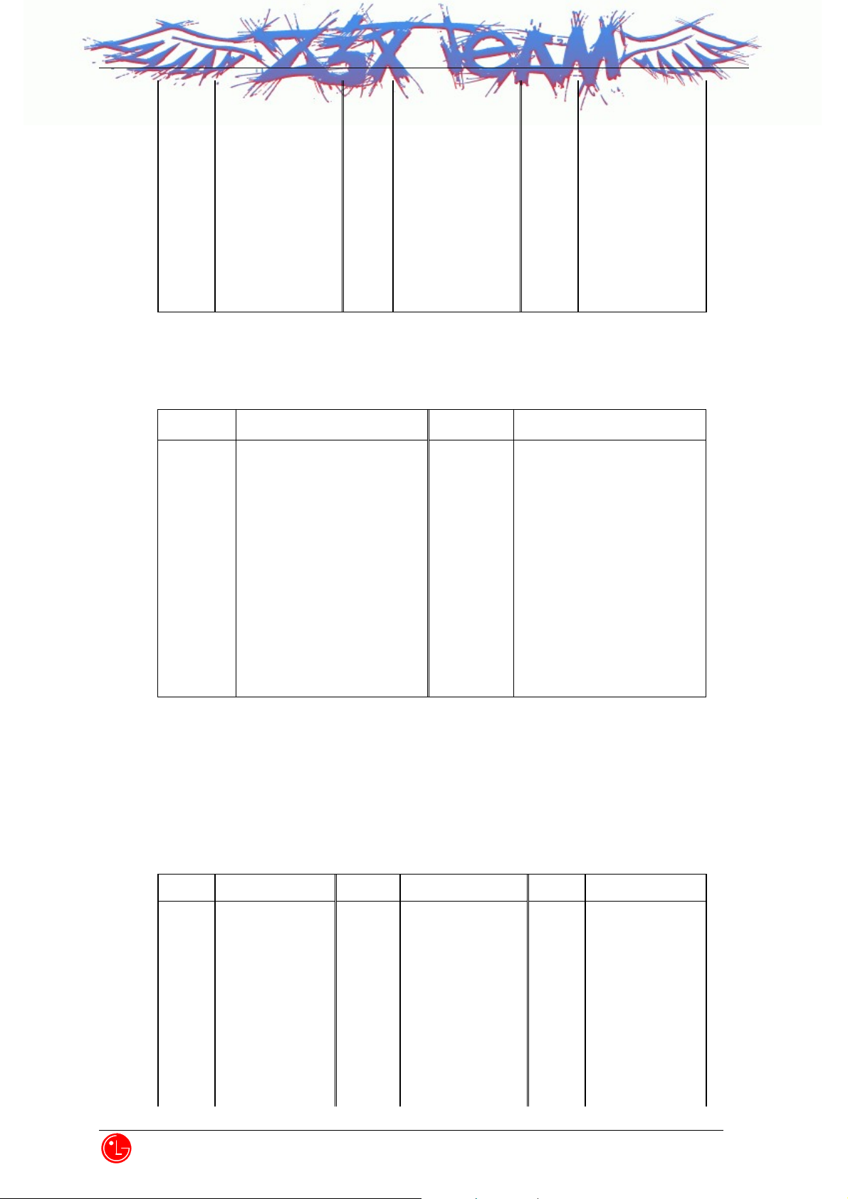
1. In idle state, Press ‘##83587’ + “000000”
2. Select ‘1.NAM1’ or ‘2.NAM2’ to see each parameter.
(Except ESN)
● Usually pressing ‘OK key’ will save the change.
● To exit Service Program, press ‘END’ key.
LG Electronics Inc.
Z3X-BOX.COM
- 1 -
Page 17
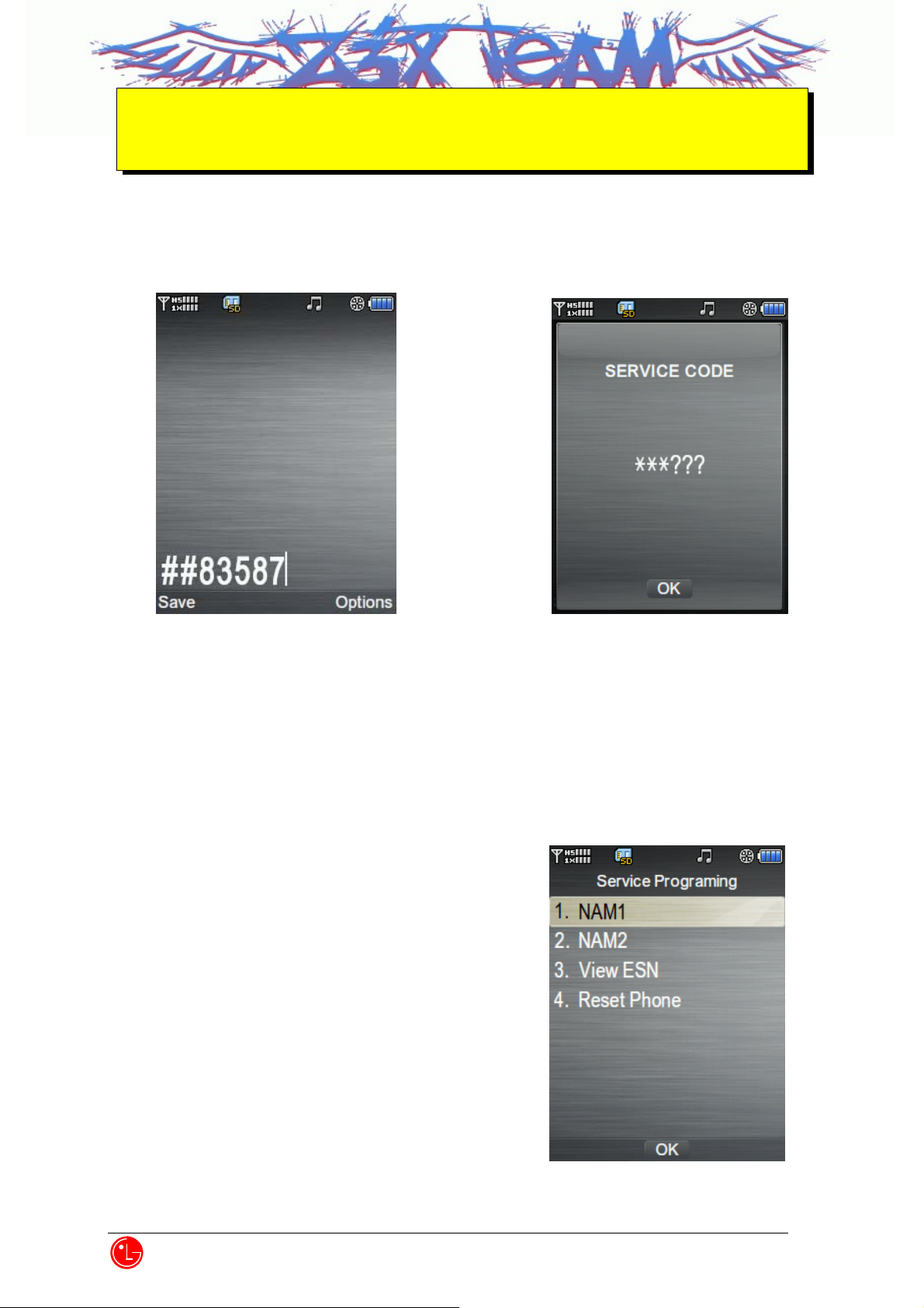
2-1) NAM1 Setting
After select ‘1.NAM1’, you can see this Entrance
screen for for NAM1 setting.
Press ‘OK key’ to edit NAM1 items.
Press ‘CLR key’ to go to the main page.
(NAM2 settingwill show you same screen when you
select ‘2.NAM2’)
2-2) NAM1 Phone Number (MDN)
You can edit NAM1 Phone Number(MDN).
Press ‘OK key’ to edit more NAM1 items.
Press ‘CLR key’ to edit previous NAM1 items.
Z3X-BOX.COM
2-3) NAM1 Phone Number (MIN)
You can edit NAM1 Phone Number(MIN).
Press ‘OK key’ to edit more NAM1 items.
Press ‘CLR key’ to edit previous NAM1 items.
LG Electronics Inc.
- 2 -
Page 18
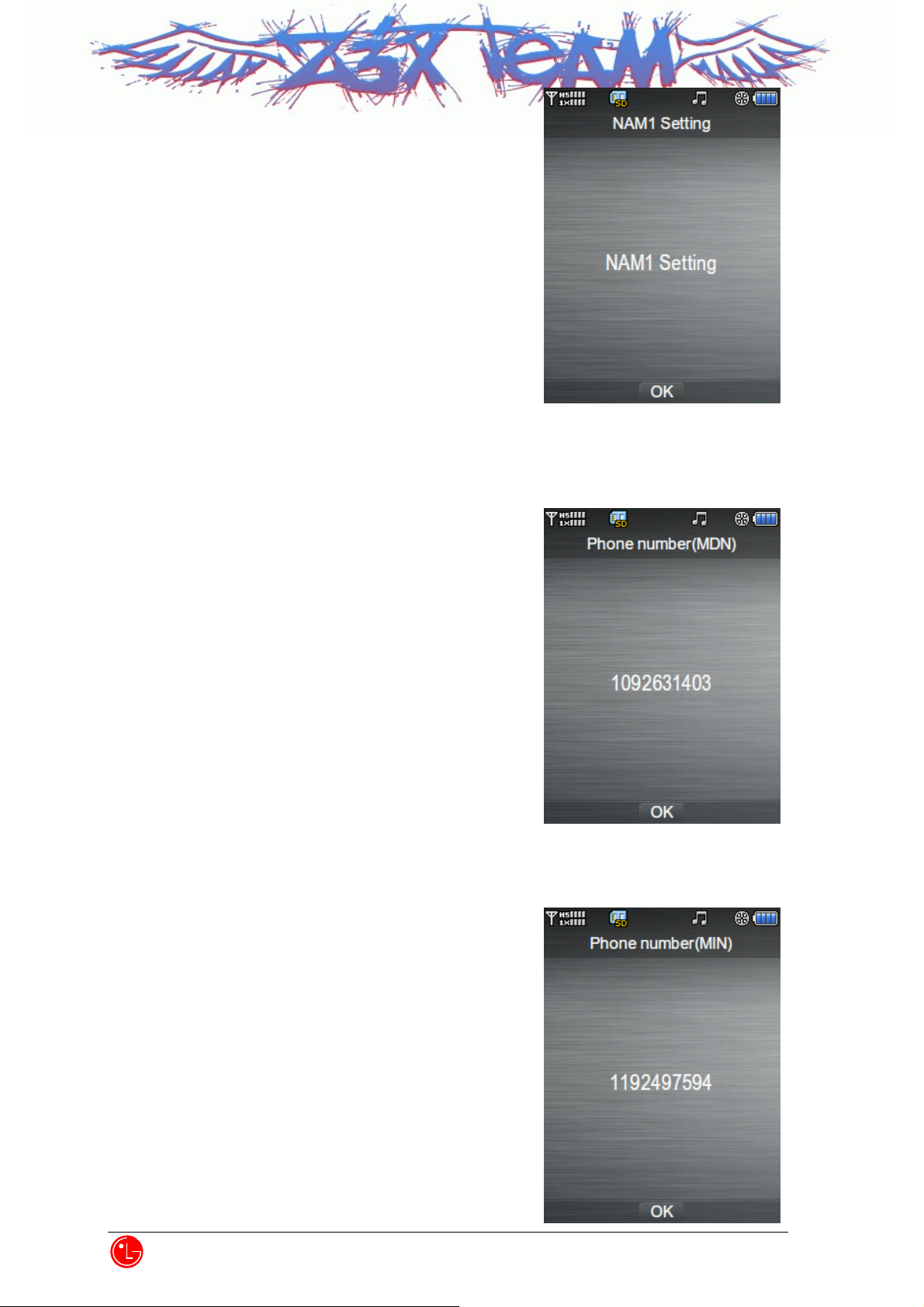
2-4) NAM1 Home SID
You can edit NAM1 Home SID.
Press ‘OK key’ to edit more NAM1 items.
Press ‘CLR key’ to edit previous NAM1 items.
2-5) NAM1 Name
You can edit NAM1 Name.
Press ‘OK’ to edit more NAM1 items.
Press ‘Soft Key 1’ to edit NAM1 Name.
Press ‘CLR key’ to edit previous NAM1 items.
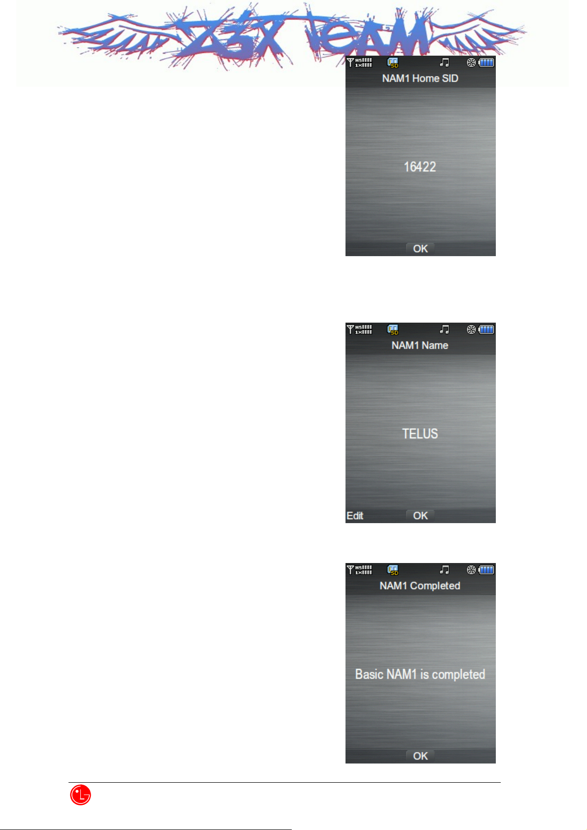
2-6) More NAM1 Programming
You can decide to edit more NAM1 items.
Press ‘END key’ to exit Service Programming.
Press ‘OK key’ to edit more advanced NAM1 items.
Z3X-BOX.COM
LG Electronics Inc.
- 3 -
Page 19
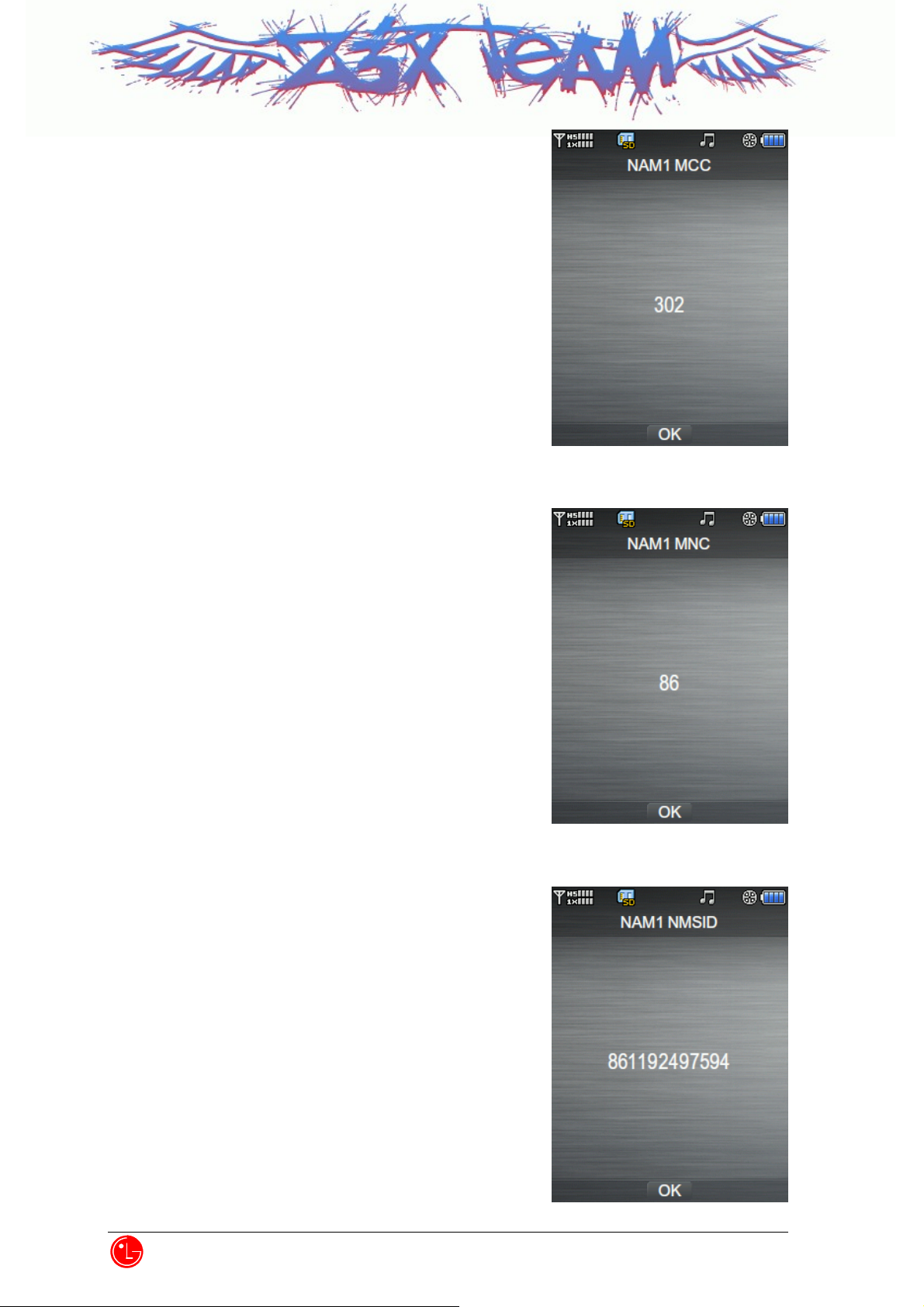
2-7) NAM1 MCC
You can edit NAM1 Mobile Country Code.
Press ‘OK key’ to edit more NAM1 items.
Press ‘CLR key’ to edit previous NAM1 items.
2-8) NAM1 MNC
You can edit NAM1 MNC.
Press ‘OK key’ to edit more NAM1 items.
Press ‘CLR key’ to edit previous NAM1 items.
2-9) NAM1 NMSID
You can edit NAM1 MNC.
Press ‘OK key’ to edit more NAM1 items.
Press ‘CLR key’ to edit previous NAM1 items.
Z3X-BOX.COM
LG Electronics Inc.
- 4 -
Page 20
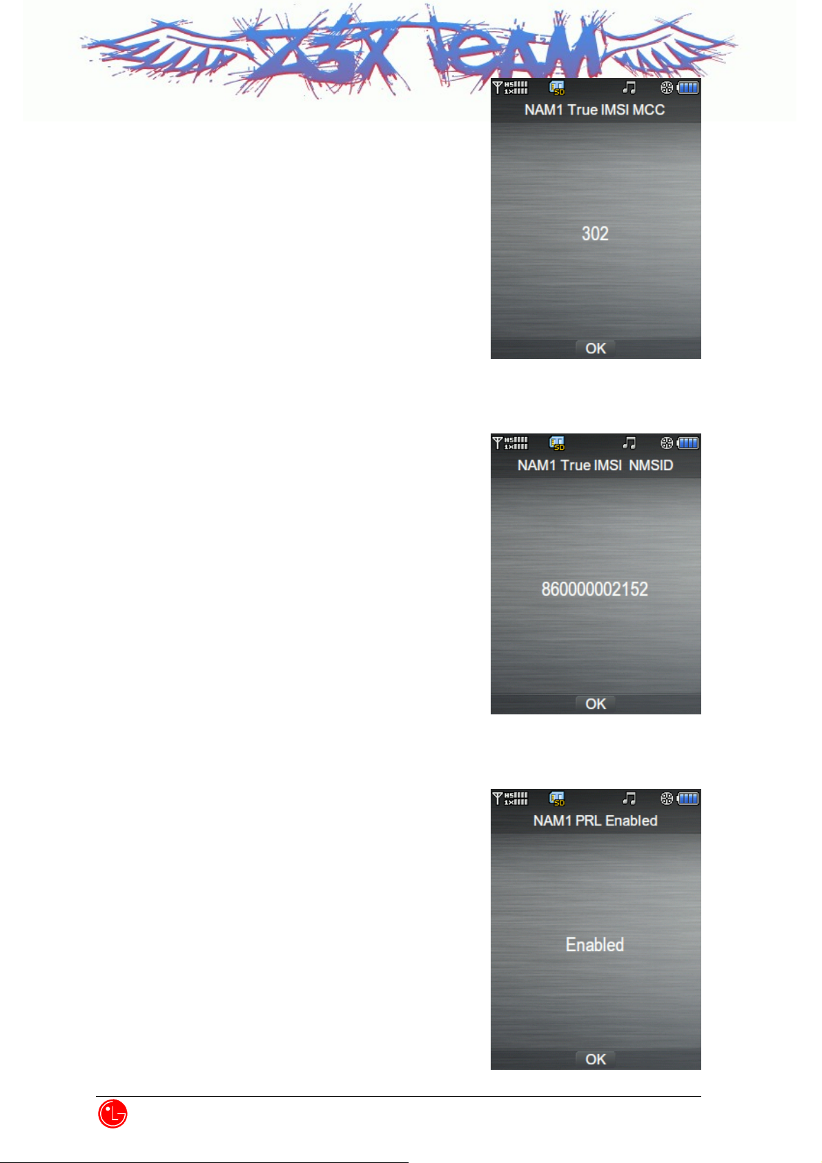
2-10) NAM1 True IMSI MCC
You can edit NAM1 True IMSI MCC.
Press ‘OK key’ to edit more NAM1 items.
Press ‘CLR key’ to edit previous NAM1 items.
2-11) NAM1 True IMSI NMSID
You can edit NAM1 True IMSI NMSID.
Press ‘OK key’ to edit more NAM1 items.
Press ‘CLR key’ to edit previous NAM1 items.
2-12) NAM1 PRL Enabled
You can see NAM1 PRL Enabled.
Press ‘OK key’ to edit more NAM1 items.
Press ‘CLR key’ to edit previous NAM1 items.
Z3X-BOX.COM
LG Electronics Inc.
- 5 -
Page 21
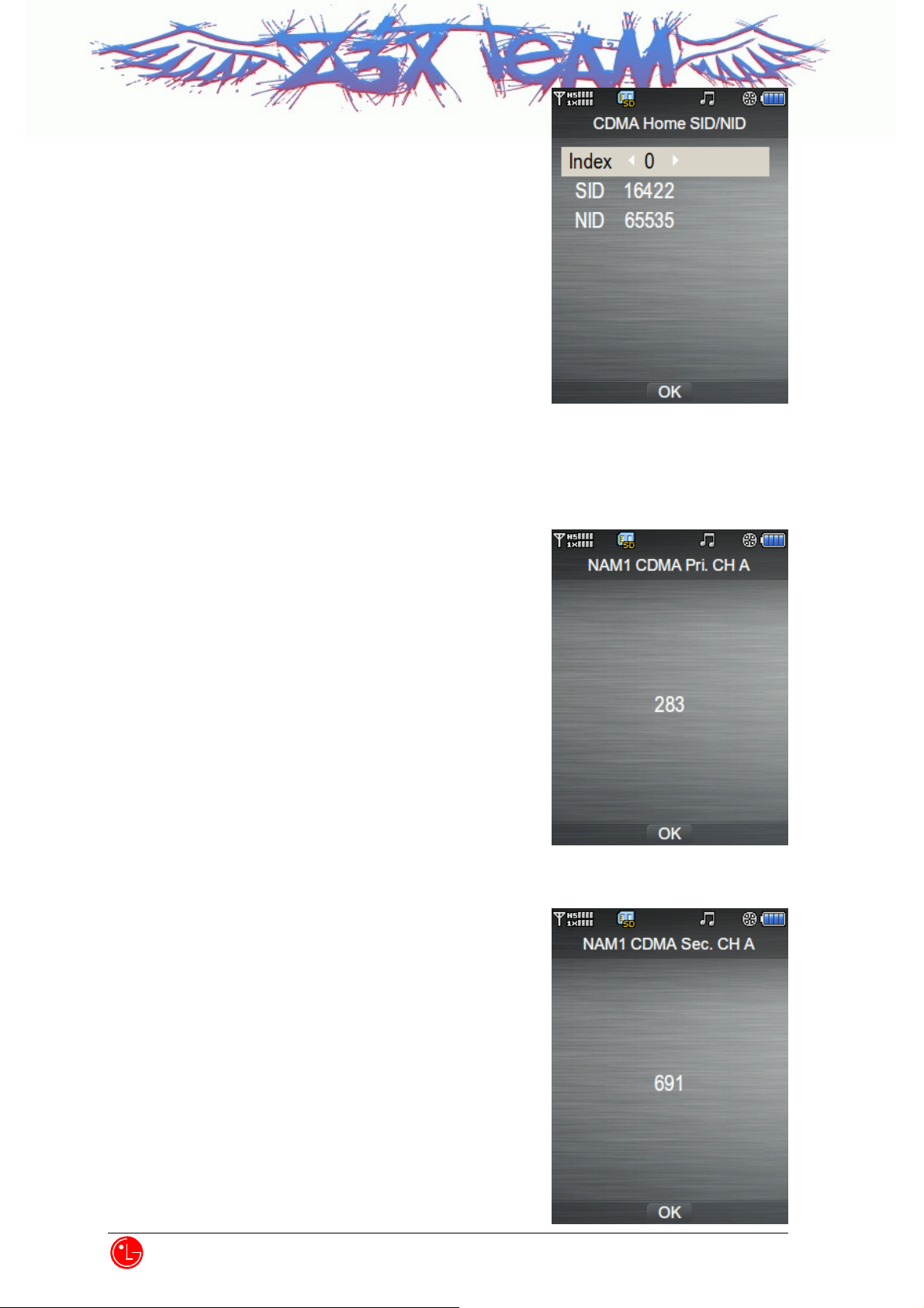
2-13) CDMA Home SID/NID
You can edit NAM1 Home SID/NID Pairs.
Press ‘OK key’ to edit more NAM1 items.
Press ‘CLR key’ to edit previous NAM1 items.
2-14) NAM1 CDMA Pri. CH A
You can edit NAM1 CDMA Primary Channel A.
Press ‘OK key’ to edit more NAM1 items.
Press ‘CLR key’ to edit previous NAM1 items.
Z3X-BOX.COM
2-15) NAM1 CDMA Sec. CH A
You can edit NAM1 CDMA Secondary Channel A.
Press ‘OK key’ to edit more NAM1 items.
Press ‘CLR key’ to edit previous NAM1 items.
LG Electronics Inc.
- 6 -
Page 22
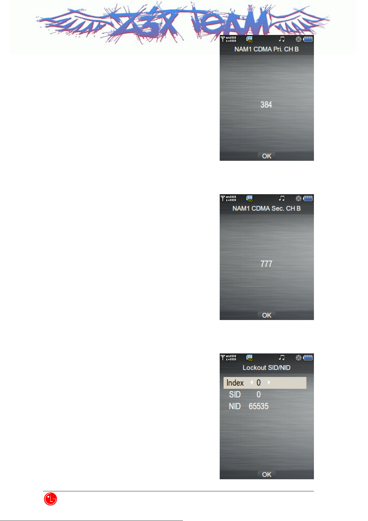
2-16) NAM1 CDMA Pri. CH B
You can edit NAM1 CDMA Primary Channel B.
Press ‘OK key’ to edit more NAM1 items.
Press ‘CLR key’ to edit previous NAM1 items.
2-17) NAM1 CDMA Sec. CH B
You can edit NAM1 CDMA Secondary Channel B.
Press ‘OK key’ to edit more NAM1 items.
Press ‘CLR key’ to edit previous NAM1 items.
2-18) Lockout SID/NID
You can edit Lockout SID/NID Pairs.
Press ‘OK key’ to edit more NAM1 items.
Press ‘CLR key’ to edit previous NAM1 items.
Z3X-BOX.COM
LG Electronics Inc.
- 7 -
Page 23
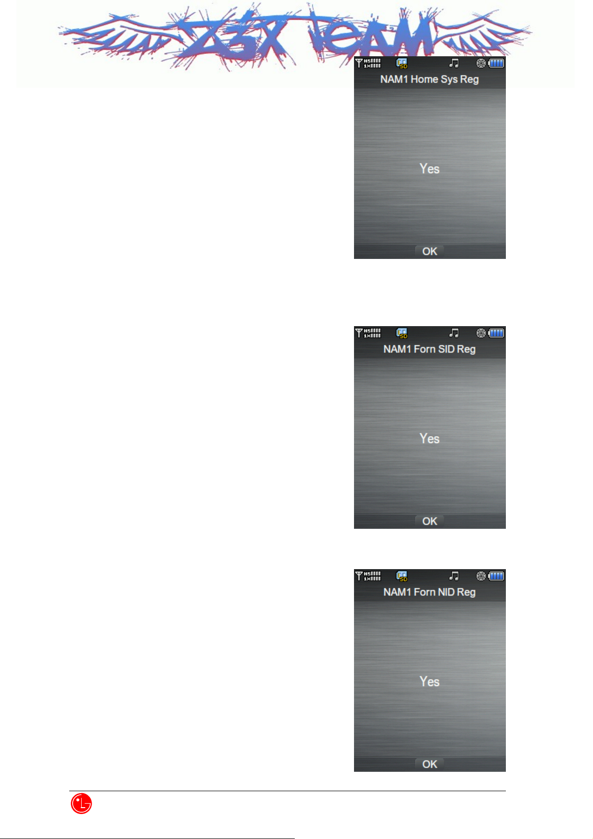
2-19) NAM1 Home Sys Reg
You can edit Home System Registration.
Press ‘OK key’ to edit more NAM1 items.
Press ‘CLR key’ to edit previous NAM1 items.
Press Left, Right, Up, Down key to toggle Yes/No.
2-20) NAM1 Forn SID Reg
You can edit NAM1 Foreign SID Registration.
Press ‘OK key’ to edit more NAM1 items.
Press ‘CLR key’ to edit previous NAM1 items.
Press Left, Right, Up, Down key to toggle Yes/No.
2-21) NAM1 Forn NID Reg
You can edit NAM1 Foreign NID Registration.
Press ‘OK key’ to edit more NAM1 items.
Press ‘CLR key’ to edit previous NAM1 items.
Press Left, Right, Up, Down key to toggle Yes/No.
Z3X-BOX.COM
LG Electronics Inc.
- 8 -
Page 24
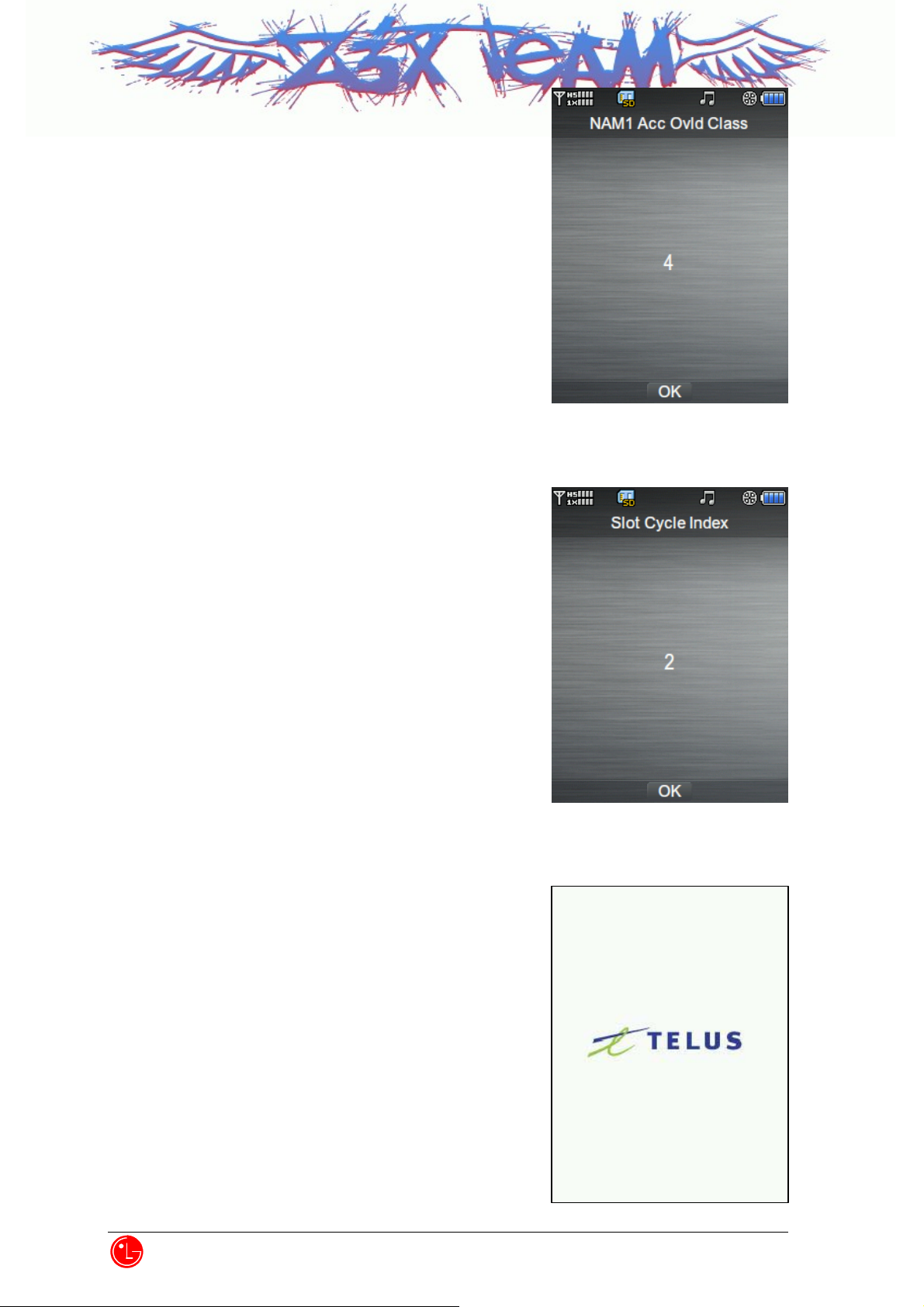
2-22) NAM1 Acc Ovld Class
You can see NAM1 Access Overload Class.
Press ‘OK key’ to edit more NAM1 items.
Press ‘CLR key’ to edit previous NAM1 items.
2-23) Slot Cycle Index
You can edit Slot Cycle Index
Press ‘OK key’ to edit more NAM1 items.
Press ‘CLR key’ to edit previous NAM1 items.
2-24) Powering Down
Restart.
Z3X-BOX.COM
LG Electronics Inc.
- 9 -
Page 25
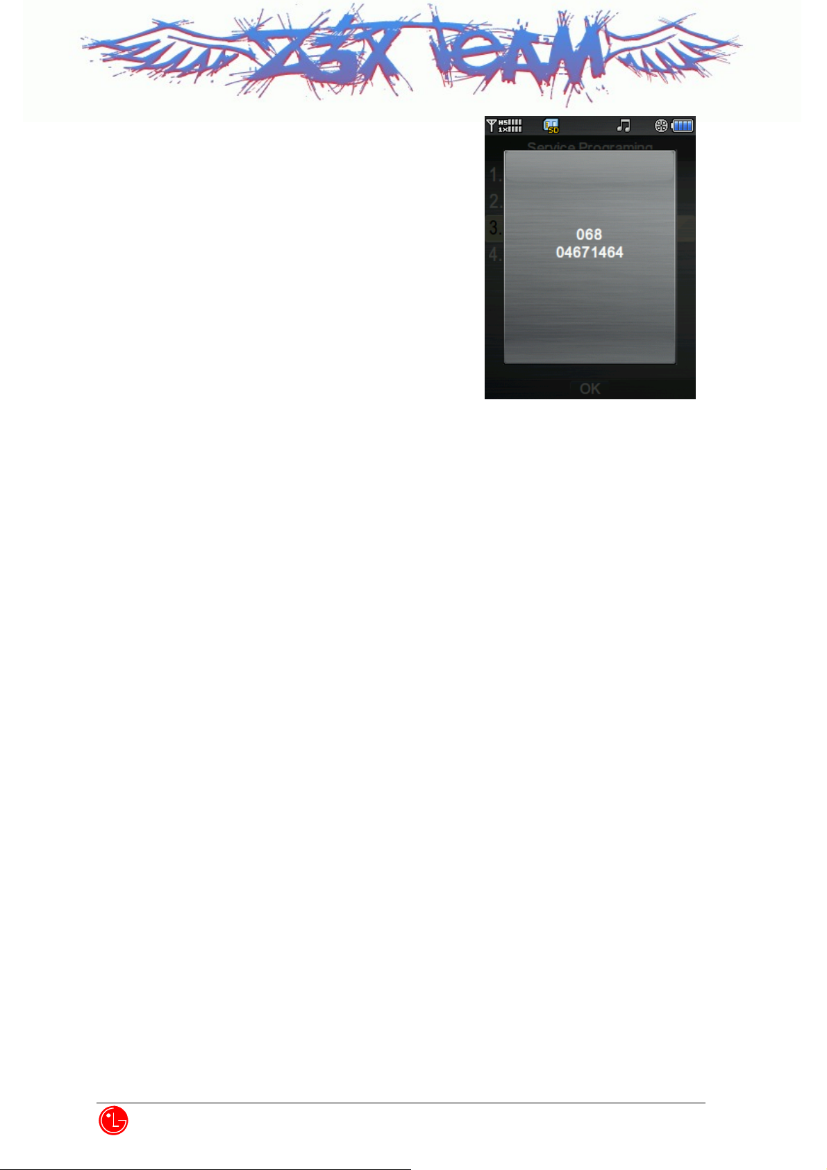
2-25) ESN
You can see the ESN number by select ‘3.View ESN’
from Service Programing main menu.
It will be shown as decimal format.
ESN can’t be modified.
Z3X-BOX.COM
LG Electronics Inc.
- 10 -
Page 26

CX8700
CHAPTER 3. Circuit Description
1. RF Transmit/Receive Part
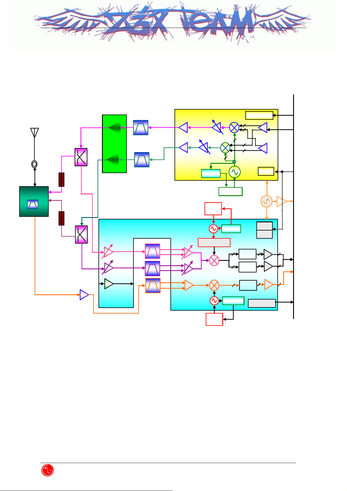
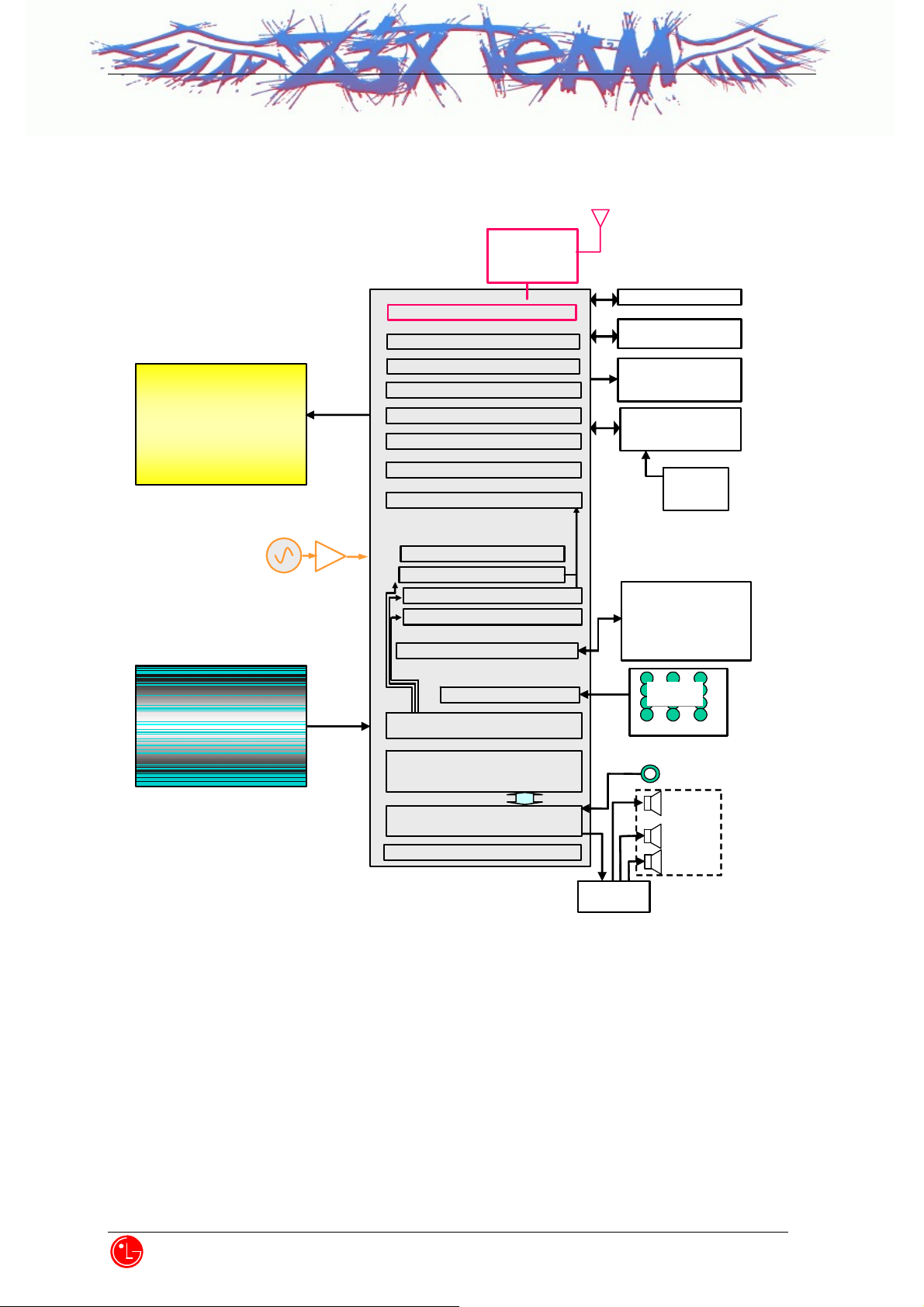
1.1 Overview
The TX and RX part employs the Direct-Conversion system. The TX and RX frequencies are
respectively 824.04~848.97 and 869.04~893.97 for cellular and 1850~1910 and 1930~1990 for
PCS. The block diagram is shown in [Figure 1-1]. RF signals received through the antenna are
seperated by the Triplexer.
RF Signal fed into the low noise amplifier in RFR6500(LNA) through the duplexer. Then, they are
fed into Mixer in RFR6500. In RFR6500, the RF signal is changed into baseband signal directly.
Then, this signal is changed into digital signal by the analog to digital converter (ADC, A/D
Converter), and the digital circuit part of the MSM(Mobile Station Modem) 6500 processes the
data from ADC. The digital processing part is a demodulator.
In the case of transmission, RFT6150 receives OQPSK-modulated anlaog signal from the
MSM6550.
The RFT6150 connects directly with MSM6550 using an analog baseband interface. In RFT6150,
the baseband quadrature signals are upconverted to the Cellular or PCS frequency bands and
amplified to provide signal drive capability to the power amp.
After that, the RF signal is amplified by the Power Amp in order to have enough power for
radiation. Finally, the RF signal is sent out to the cell site via the antenna after going through
the duplexer.
Z3X-BOX.COM
LG Electronics Inc.
- 26 -
Page 27
CX8700
[Figure 1-1] Block Diagram of CX8700
Tri-band Ant.
U103
Mobile S/W
MS-156NB
Triplexer
GPS BPF
U104
Triplexer
C015
PCS Duplexer
ACMD-7402
DCN Duplexer
EFSD836MF2S2
DP101
U109
COUPLER
CP0402A1880
U110
COUPLER
CP0402A836
DP104
U107
GPS LNA
ALM-1106-TR1
U108
DUAL PAM
AWT6310R
Gain:27dB
Gain:15.9dB
NF:1.6dB
Gain:15.4dB
NF:1.4dB
Gain:15.4dB
NF:1.4dB
F104
PCS Tx RF BPF
ACPF -7002
IL:3.5dB
Attn.:35dB
F105
DCN Tx RF SAW
EFCH836MT CB 8
IL:2.5dB
Attn.:39dB
F102
PCS Rx RF SAW
B7847
IL:3.4dB
GPS Rx RF SAW
DCN Rx RF SAW
EFCH881MT CA7
IL:2.5dB
F103
B7840
F101
RFR6500
RFR6000
U105
RFT6150
RFT6150
TX PLL
Loop
Filter
LO Distribution
Loop
Filter
U102
Loop Filer
RX PLL
GPS PLL
Gain Control
X101
VCTCXO
TG-5010LH
LPF
LPF
LPF
Secondary path
Jammer Det.
SBI 1
SBI 1
SBI 2
Primary path
M
S
M
6
5
5
0
Z3X-BOX.COM
LG Electronics Inc.
- 27 -
Page 28
CX8700
BLUETOOTH
RF
MODULE
RFT6150
VCTCXO
RFR6500
BT 1.2 PROCESS
JTAG Interface
ARM9 Core
R-UIM Controller
RF Interface
MSM6550
DFM processor
CDMA processor
gpsOne processor
Memory Controller
QDPS4000
- VOCODER
- MIDI(CMX) etc.
HK ADC
SBI
Tx DACs
PLL
Rx ADCs
CODEC
USB
GPIO
T-Flash MEMORY
CAMERA Module
2M Pixels
LCD MODULE
262K TFT Main
65K TFT Sub
PMIC
MAX1829
Battery
MCP MEMORY
1G NAND Flash
512M SDRAM
(TY9000A000AMGP)
KEYPAD
Mic
EARPIECE
Stereo SPK
Z3X-BOX.COM
LG Electronics Inc.
AUDIO AMP
(LM4857)
- 28 -
Page 29
CX8700
1.2 Description of RX Part Circuit
1.2.1 Triplexer Filter (U104)
The main function of Triplexer is to prohibit the other band signals from flowing into the one
band circuit and vice versa. RF designer can use common tri-band antenna regardless of
frequency band (800, 1575 and 1900 MHz). The specification of CX8700 Triplexer is described
below:
Cellular GPS PCS
Frequency Range 824 – 894 MHz 1575.42 MHz 1850 – 1990 MHz
Insertion Loss to
Common
Isolation
Temperature Range -30 to +85 deg
1.2.2 Duplexer (DP104, DP101)
1.0 dB Max
(At +25 deg)
48.5dB
(Cell TX)
1.8 dB Max.
(At +25 deg)
32.9dB(GPS-Cell)
18.3(GPS-PCS)
0.85 dB Max
(At +25 deg)
53.1dB
(PCS TX)
The duplexer consists of the RX bandpass filter (BPF) and the TX BPF which has the function of
separating TX and RX signals in the full duplex system for using the common antenna. The TX
part BPF is used to suppress noises and spurious out of the TX frequency band. The RX BPF is
used to receive only RX signal coming from the antenna, which is usually called preselector.
It’ s main function is to limit the bandwidth of spectrum reaching the LNA and mixer, attenuate
receiver spurious response and suppress local oscillator energy. As a result frequency
sensitivity and selectivity of mobile phone increase. The specification of CX8700 duplexer
described below ;
z PCS duplexer:
Z3X-BOX.COM
TX RX TX to RX (min)
Pass Band 1850~1910 MHz 1930~1990 MHz
Insertion Loss 3.5dB max 3.0dB max
Return Loss 8.0dB min 8.0dB min
Attenuation
LG Electronics Inc.
(1930~1990MHz)
40dB min
50dB min
(1850~1910MHz)
54dB (1850~1910MHz)
44dB (1930~1990MHz)
- 29 -
Page 30
CX8700
z Cellular duplexer
TX RX TX to RX (min)
Pass Band 824~849 MHz 869~894 MHz
Insertion Loss 2.5B max 3.5dB max
VSWR 2.2 max 2.3 max
Attenuation 40dB min (869~894MHz)
1.2.3 LNA (U105)
The RFR6500 has cellular, and PCS LNA, respectively. The characteristics of Low Noise
Amplifier (LNA) are low noise figure, high gain, high intercept point and high reverse isolation.
The frequency selectivity characteristic of mobile phone is mostly determined by LNA.
The specification of CX8700 LNA is described below:
Parameter
Gain -19 -20 -2 -9 15.5 16 dB
Noise Figure 19 20 2 9 1.4 1.6 dB
Input IP3 25 25 20 20 6 8 dBm
1.2.4 GPS LNA(U107)
Low gain Middle gain High gain Units
Cellular PCS Cellular PCS Cellular PCS
50dB min
(824~849MHz)
54dB (824~849MHz)
43dB (869~894MHz)
The characteristics of Low Noise Amplifier (LNA) are low noise figure, high gain, high intercept
point and high reverse isolation. The frequency selectivity characteristic of mobile phone is
mostly determined by LNA.
The specification of CX8700 GPS LNA is described below
Z3X-BOX.COM
Parameter GPS Band Units
Gain 14.8 dB
Noise Figure 0.85 dB
1dB compression point 0 dBm
IIP3 +5 dBm
1.2.5 RX RF SAW FILTER(F101, F102, F103)
The main function of RX RF SAW filter is to attenuate mobile phone spurious frequency,
attenuate noise amplified by the LNA and suppress second harmonic originating in the LNA.
LG Electronics Inc.
- 30 -
Page 31

CX8700
1.2.6 Down-converter Mixers (U105)
The RFR6500 device performs signal down-conversion for Cellular, PCS and GPS tri-band
applications. It contains all the circuitry (with the exception of external filters) needed to support
conversion of received RF signals to Base-band signals. The three down-converting Mixers
(Cellular, PCS and GPS), and a programmable PLL for generating RX LO frequency and an RX
LO Buffer Amplifier and RX Voltage Controlled Oscillator. The GPS LNA & mixers offer the most
advanced and integrated CDMA RX solution designed to meet cascaded Noise Figure (NF) and
Third-order Intercept Point (IIP3) requirements of IS-98D and J-STD-018 specifications for
Sensitivity, Two-Tone Inter-modulation, and Single-tone Desensitization.
Operation modes and band selection are specially controlled from the Mobile Station Modem
MSM6550.
The specification of CX8700 Mixers is described below:
Parameter
Noise Figure 27 27 11 11 dB
Input IP3 4 3 4 3 dBm
Input IP2 50 50 75 70 dBm
Low gain High gain Units
Cellular PCS Cellular PCS
1.3 Description of Transmit Part Circuit
1.3.1 RFT6150 (U102)
The RFT6150 Base-band to RF Transmit Processor performs all TX signal-processing
functions required between digital Base-band and the Power Amplifier Modulator (PAM). The
Base-band quadrate signals are up-converted to the Cellular or PCS frequency bands and
amplified to provide signal drive capability to the PAM. The RFT6100 includes an mixers for
up-converting analog Base-band to RF, a programmable PLL for generating TX LO frequency
an TX LO Buffer Amplifier and TX Voltage Controlled Oscillator, cellular and PCS driver
Z3X-BOX.COM
amplifiers and TX power control through an 85 dB VGA. As added benefit, the single sideband
up-conversion eliminates the need for a band pass filter normally required between the
up-converter and driver amplifier.
I, I/, Q and Q/ signals proceed from the MSM6550 to RFT6150 are analog signal. In CDMA
mode, These signals are modulated by Offset Quadrature Phase Shift King (OQPSK). I and Q
are 90 deg. out of phase, and I and I/ are 180 deg. The mixers in RFT6150 converts baseband
signals into RF signals. After passing through the upconverters, RF signal is inputted into the
Power AMP.
LG Electronics Inc.
- 31 -
Page 32

CX8700
z RFT6150 Cellular and PCS CDMA RF Specifications
Parameter Condition Min. Type. Max. Units
Rated Output Power
Min Output Power
RX band noise power
ACPR
Average CDMA Cellular
Average CDMA PCS
Average CDMA Cellular
Average CDMA PCS
CDMA Cellular
CDMA PCS
Cellular: Fc±885kHz
PCS : Fc±1.25MHz
8
10
-80
-78
-133
-132
-56
-56
dBm
dBm
dBm
dBm
dBm/Hz
dBc/
30kHz
1.3.2 Power Amplifier(U108)
The Dual power amplifier that can be used in the PCS and CDMA mode has linear amplification
capability and high efficiency. For higher efficiency, it is made up of one MMIC (Monolithic
Microwave Integrated Circuit) for which RF input terminal and internal interface circuit are
integrated onto one IC after going through the AlGaAs/GaAs HBT (heterojunction bipolar
transistor) process. The module of power amplifier is made up of an output end interface circuit
including this MMIC. The maximum power that can be inputted through the input terminal is
+17dBm and conversion gain is about 28dB. RF transmit signals that have been amplified
through the power amplifier are sent to the duplexer.
.
1.4 Description of Frequency Synthesizer Circuit
1.4.1 Voltage Control Temperature Compensation Crystal Oscillator (VCTCXO, X101)
The temperature variation of mobile phone can be compensated by VCTCXO. The reference
frequency of a mobile phone is 19.2 MHz. The receiver frequency tuning signals called
TRK_LO_ADJ from MSM as 0.5 V~2.5 V DC via R and C filter in order to generate the reference
frequency of 19.2 MHz and input it into the frequency synthesizer. Frequency stability
depending on temperature is ±2.0 ppm.
Z3X-BOX.COM
LG Electronics Inc.
- 32 -
Page 33

CX8700
2. Digital/Voice Processing Part
2.1 Overview
The digital/voice processing part processes the user's commands and processes all the digital and voice signal
processing in order to operate in the phone. The digital/voice processing part is made up of a keypad/LCD,
receptacle part, voice processing part, mobile station modem part, memory part, and power supply part.
2.2 Configuration
2.2.1 Keypad/LCD and Receptacle Part
This is used to transmit keypad signals to MSM6550. It is made up of a keypad backlight part that illuminates
the keypad, LCD part that displays the operation status onto the screen, and a receptacle that receives and sends
out voice and data with external sources.
2.2.2 Voice Processing Part
The voice processing part is made up of an audio codec used to convert MIC signals into digital voice signals
and digital voice signals into analog voice signals, amplifying part for amplifying the voice signals and sending
them to the ear piece, amplifying part that amplifies ringer signals coming out from MSM6550, and amplifying
part that amplifies signals coming out from MIC and transferring them to the audio processor.
2.2.3 MSM (Mobile Station Modem) 6500 Part
MSM is the core elements of CDMA terminal and carries out the functions of CPU, encoder, interleaver,
deinterleaver, Viterbi decoder, Mod/Demod, and vocoder.
2.2.4 Memory Part
Z3X-BOX.COM
The memory part is made up of a NAND Flash memory and a SDRAM for storing data.
2.2.5 Power Supply Part
The power supply part is made up of circuits for generating various types of power, used for the digital/voice
processing part.
LG Electronics Inc.
- 33 -
Page 34

CX8700
2.3 Circuit Description
2.3.1 Keypad/LCD and Receptacle Part
Once the keypad is pressed, the key signals are sent out to MSM6550 for processing. In addition, when the key
is pressed, the keypad/LCD lights up through the use of 18 LEDs. The terminal status and operation are
displayed on the screen for the user with the characters and icons on the LCD.
Moreover, it exchanges audio signals and data with external sources through the receptacle, and then receives
power from the battery or external batteries.
2.3.2 Audio Processing Part
MIC signals are amplified through OP AMP, inputted into the audio codec(included in MSM6550) and
converted into digital signals. Oppositely, digital audio signals are converted into analog signals after going
through the audio codec. These signals are amplified at the audio amplifier and transmitted to the ear-piece. The
signals from MSM6550 activate the ringer by using signals generated in the timer in MSM6550.
2.3.3 MSM Part
MSM6550 is the core element of CDMA system terminal that includes ARM926EJ-S microprocessor core. It
supports both CDMA and Digital FM, operating in both the cellular and PCS spectrums. The subsystems within
the MSM6550 include a CDMA processor, a DFM processor, a multi-standard Vocoder, an integrated CODEC
with earpiece and microphone amplifiers, general-purpose ADC for subsytem monitoring, an ARM926EJ-S
microprocessor, and an RS-232 serial interfaces supporting forward and reverse link MDR data communications
of 230.4 Kbps simultaneously. And it also contains complete digital modulation and demodulation systems for
both CDMA and AMPS cellular standards, as specified in IS-95-A/B/C.
In MSM, coded symbols are interleaved in order to cope with multi-path fading. Each data chann el is scrambled
by the long code PN sequence of the user in order to ensure the confidentiality of calls. Moreover, binary
quadrature codes are used based on walsh functions in order to discern each channel. Data created thus are
4-phase modulated by one pair of Pilot PN code and they are used to create I and Q data.
When received, I and Q data are demodulated into symbols by the demodulator, and then de-interleaved in
reverse to the case of transmission. Then, the errors of data received from viterbi decoder are detected and
corrected. They are voice-decoded at the vocoder in order to output digital voice data.
Z3X-BOX.COM
LG Electronics Inc.
- 34 -
Page 35

CX8700
B/T Chip
B/T Chip
Antenna
Antenna
RFR6000
RFR6500
POWER
POWER
Amplifier
Amplifier
VCTCXO
VCTCXO
+2.9V_Rx_LDO
+2.9V_Rx_LDO
RFT6100
RFT6150
Bluetooth RF
Bluetooth RF
19.2MHz
19.2MHz
INNER CHG
INNER CHG
BATTERY
BATTERY
HDET
HDET
RF Controls
RF Controls
Bluetooth
Bluetooth
Baseband
Baseband
Processor
Processor
PLL
PLL
HK ADC
HK ADC
Rx
Rx
ADCs
ADCs
RF
RF
Interface
Interface
TX
TX
DACs
DACs
AUX
AUX
SBI
SBI
SBI
SBI
MSM6500
MSM6500
Mobile Station Modem
Mobile Station Modem
gpsOne
gpsOne
Processor
Processor
CDMA
CDMA
Processor
Processor
DFM
DFM
Processor
Processor
JTAG Interfaces
JTAG Interfaces
UART1
UART1
UART2
UART2
UART3/USB
UART3/USB
Integrated
Integrated
MODE Select
MODE Select
Interface
Interface
ETM
ETM
CAMIF
CAMIF
ARM9
ARM9
TDMI
TDMI
Memory
Memory
Controller
Controller
General-
General-
Purpose
Purpose
Interface
Interface
Vocoder
Vocoder
EVRC
EVRC
13k
13k
MP4
MP4
MIDI
MIDI
QDSP4000
QDSP4000
CODEC
CODEC
Data Comm
Data Comm
DM
DM
USB
USB
USB
USB
Transceiver
Transceiver
LDO
LDO
Camera module
Camera module
(1.3M C-MOS)
(1.3M C-MOS)
Microprocessor Bus
Microprocessor Bus
Address/Data
Address/Data
General-Purpose Interface Bus
General-Purpose Interface Bus
1 2 3
1 2 3
4 5 6
Keypad input
Keypad input
2
2
2
2
4 5 6
7 8 9
7 8 9
* #0
* #0
Audio AMP
Audio AMP
EAR
EAR
MIC
MIC
Digital Test Bus JTAG
Digital Test Bus JTAG
PC
PC
Connectivity
Connectivity
Test/Debug
Test/Debug
System
System
Memory
Memory
NAND Flash(512Mb)
NAND Flash(512Mb)
LP-SDRAM(256Mb)
LP-SDRAM(512Mb)
KEYPAD, BEZEL,
KEYPAD, BEZEL,
SIIDEKEY
SIIDEKEY
Speaker
Speaker
External
External
EAR/MIC
EAR/MIC
LCD
LCD
Peripheral Circuits
Peripheral Circuits
[Figure 2-2] Block Diagram of Digital/Voice Processing Part
2.3.4 Memory Part
MCP contents 512Mbits NAND FLASH memory and 256Mbits SDRAM. In the NAND Flash Memory part of
MCP are programs used for terminal operation. The programs can be changed through downloading after the
assembling of terminals. On the SDRAM data generated during the terminal operation are stored temporarily.
2.3.5 Power Supply Part
When the battery voltage (+4.0V) is fed and the PWR key of keypad is pressed, U402(PMIC) is activated by the
PWR_ON_SW signal, and The PWRON signal is held high, Buck and LDO1,2,3 are turned on; when LDO1
reaches 87% of its final value a 60ms reset timer is started at after which RESET\ is asserted high. Now the
BB Processor is initialized and will assert PWRHOLD high. PWRHOLD maintains the power on.
Z3X-BOX.COM
The Buck/LDO1,2,3 are generating the +1.4V_MSMC, +2.6V_MSMA, +1.8V_MSMP1 and +2.8V_LCD
respectively.
The Rx part LDO(Out5) is operated by the control signal SLEEP/ from MSM6550
The Tx part LDO(Out7) is operated by the control signal IDLE/ from MSM6550.
The TCXO part LDO(U403) is operated by the control signal TCXO_EN/ from MSM6550.
LG Electronics Inc.
- 35 -
Page 36

CX8700
2.3.6 Logic Part
The logic part consists of internal CPU of MSM, RAM, MCP. The MSM6550 receives TCXO (=19.2MHz)
from the X101 and controls the phone in CDMA modes. The major components are as follows:
z
The ARM926J-S microprocessor includes a 3 stage pipelined RISC architecture, both 32-bit ARM and 16-bit
THUMB instruction sets, a 32-bit address bus, and a 32-bit internal data bus. It has a high performance and
low power consumption.
CPU
z
NAND Flash is used to store the terminal’s program. Using the down-loading program, the program can be
changed even after the terminal is fully assembled.
SDRAM is used to store the internal flag information, call processing data, and timer data.
z
For key recognition, key matrix is setup using KYPD[1][3][5][7][9][11][13][15][17][19][21] signal from
MSM6550. 18 LEDs and backlight circuitry are included in the keypad for easy operation in the dark.
z
LCD module contains a controller which will display the information onto the LCD by 16-bit data from the
MSM6550. It is also supplied stable +2.8V_LCD by Out3 in U402 for fine view angle and LCD reflects to
improve the display efficiency. 4 LEDs is used to display LCD backlight.
MCP
KEYPAD
LCD MODULE
LG Electronics Inc.
Z3X-BOX.COM
- 36 -
Page 37

CX8700
R
R
p
ply
CHAPTER 4. Trouble Shooting
4.1.1 DCN Rx
Test Point
DCN_Duplexer
Mobile S/W
Triplexer
PCS_Duplexer
RFR6500
VCTCXO
Checking Flow
START
x
TE
ST SETUP (HHP)
- Test Channel: 384
- Test Band:
- SID: 2004
- S
Spec
Oscilloscope Setting
Z3X-BOX.COM
US Ce
llular
ecto
r Power: -30 dBm
trum Analyzer Setting
1. Check
DC P
owe
r su
circuit
2. Check
VCTCXO Circuit
3. Check
Co
ntrolsignal
4. Check
RFSign
alpath
5. Check
Rx I
/Qdata
e
downloadSW, CAL
LG Electronics Inc.
- 37 -
Page 38

CX8700
YesY
Y
4.1.1.1 Checking DC Power supply Circuit (PMIC)
Test Point Checking Flow
U302, U303
Check R319
of U303
Check
MSMP2
Check L412
of U303
+2.9V_
RX0 sOK?
No
+2.6V_
MSMP2
is OK
es
+2.9V_
es
DC Powe
is OK. See next Page
No
RX0isOK?
No
r supply Circuit
The Problem may
Refer to Logic trou
?
The Problem may
Refer to Logic trou
The Problem may
Refer to Logic trou
to
be Logic
blesh
oot
be Logic
blesh
be Logic
blesh
par
oot
oot
t
par
par
t
t
Circuit Diagram
Z3X-BOX.COM
LG Electronics Inc.
- 38 -
Page 39

CX8700
g V
T
Refer t
t
r
r
VCTCX
r
r
)
r
)
4.1.1.2 Checkin
Test Point
CTCXOCircuit
Check X101 Pin 3
◆ Refe
Check X101 Pin 4
◆ Refe
X101
to Graph 4.1.1(a
to Graph 4.1.1(b
Changing X101
Check R125, R127
C1002
SW Download
Replace Boa
19.2MHz
?
+2.8V OK?
YES
Simila
Checking Flow (VCTCXO)
No
?
NO
YES
NO
YES
d
VCTCXO
ne
Control signal
be Logic
S
Control signal
Ci
xt Page to
he Problem may
ee next Page to check
rcuit is OK.See
check
part
o Logic
O
Ci
rcuit is OK.
ou
blesh
oot
Waveform
Z3X-BOX.COM
Graph Graph
LG Electronics Inc.
- 39 -
Page 40

CX8700
Circuit Diagram
Z3X-BOX.COM
LG Electronics Inc.
- 40 -
Page 41

CX8700
r
4.1.1.3 Checking Control signal
Test Point
U105 Pin49 (SBST0)
Pin50 (SBDT0)
Check Pin 49(SBCK0),
Check if there is
Any Major Difference
Refer to Graph 4.1.1(
◆
Check Pin 49(SBCK0),
Check if there is
Any Major Difference
◆
Refer to Graph 4.1
.1(
Checking Flow
Pin 50(SBST0)
Pin 51(SBDT0) of U105
c,d
)
Z3X-BOX.COM
Pin 50(SBST0)
Pin 51(SBDT0) of U105
c,d
)
Similar?
Download the SW
Replace Board
Simila
NO
NO
?
YES
YES
Control Signal is Ok
See next Page to Check
RF signal path
Control Signal is Ok
See next Page to Check
RF signal path
LG Electronics Inc.
- 41 -
Page 42

CX8700
SB
CK0
Waveform
SB
CK0
SB
ST0
Graph 4.1.1(c)
SB
DT0
Circuit Diagram
Graph 4.1.1(d)
Z3X-BOX.COM
LG Electronics Inc.
- 42 -
Page 43

CX8700
A
◆Refer toGra
p
(e)
A
A
4.1.1.4 Checking RF Signal path (Mobile S/W, Triplexer, Duplexer)
DP101. Pin3
U104. Pin7
C1034, L111
C173
Test Point Checking Flow
U103. Pin2
DP101
U104
C1063, L185
Check U103 Pin 2
Check
if ther
e is
ny Major Difference
h 4.1.1
Check U104 Pin 7
Check
if ther
e is
ny Major Difference
◆
Ref
er to Grap
Check DP101 Pin 3
Check
if ther
ny Major Difference
◆
Ref
er to Grap
e is
h 4.1.1(f)
h 4.1.1(g)
No
No
No
No
No
Changing U104
Changing U103
Check C101
Check
C1063&L185
Changing DP101
Detected S
Detected S
Detected S
Detected S
Detected S
ignal?
Yes
ignal?
Yes
ignal?
Yes
ignal?
Yes
ignal?
Yes
No
Check
C1034 & C173
L111
Detected S
RF Signal Path
S
ee next Page to check
RX I/Q data signal
ignal?
Yes
is
OK.
.
Z3X-BOX.COM
LG Electronics Inc.
- 43 -
Page 44

CX8700
)
U103 Pin
Waveform
Graph 4.1.1(e
U104 Pin
DP101 Pin 3
Graph 4.1.1(f)
Z3X-BOX.COM
Graph 4.1.1(g)
LG Electronics Inc.
- 44 -
Page 45

CX8700
Circuit
Z3X-BOX.COM
LG Electronics Inc.
- 45 -
Page 46

CX8700
r
r
rd A
d
,
A
A
)
4.1.1.5 Checking Rx I/Q data
Test Point
U105 Pin7 (RX0_QM
Pin8 (RX0_QP)
Pin9 (RX0_IM)
Pin10 (RX0_IP)
Check Pin7 (RX0_QM)
Pin8 (RX0_QP)
Pin9 (RX0_IM)
Pin10 (RX0_IP)
Check if there is
ny Major Difference
◆ Refer to Graph 4.1.1(h,i)
Check Pin7 (RX0_QM)
Pin8 (RX0_QP)
Pin9 (RX0_IM)
Pin10 (RX0_IP)
Check if there is
ny Major Difference
◆ Refer to Graph 4.1.1(h,i)
Z3X-BOX.COM
Checking Flow
Simila
?
Yes
Re-download the
e & Calibrate
Softwa
Similar?
Yes
ll DCN RX check is complete
if the phone still does not work
change the board.
No
Replace U105
No
Replace Boa
LG Electronics Inc.
- 46 -
Page 47

CX8700
)
Waveform
RX0_IP
RX0_IM
Graph 4.1.1(h)
RX0_QP
RX0_QM
Graph 4.1.1(i
Circuit
Z3X-BOX.COM
LG Electronics Inc.
- 47 -
Page 48

CX8700
X
R
L
R
p
ply
4.1.2 PCS R
Test Point
Checking Flow
START
x
TE
ST SETUP (HHP)
- Test Channel: 600
- Test Band:
- SID: 4119
- S
Spec
Oscilloscope Setting
Z3X-BOX.COM
US
PCS
ecto
r Power: -30 dBm
trum Analyzer Setting
1. Check
DC P
owe
r su
circuit
3. Check
Co
ntrolsignal
4. Check
RFSign
alpath
2. Check
VCTCXO Circuit
5. Check
Rx I
/Qdata
e
LG Electronics Inc.
-downloadSW, C
A
- 48 -
Page 49

CX8700
T
Y
Y
4.1.2.1 Checking DC Power supply Circuit (PMIC)
Test Point Checking Flow
Circuit Diagram
Check R319
of U303
Check C318
of U302
+2.9V_
RX0 isOK?
es
+2.6V_
es
DC Powe
is OK. See next Page
No
MSMP2
is OK
No
r supply Circuit
The Problem may
Refer to Logic trou
?
he Problem may
Refer to Logic trou
to
be Logic
blesh
oot
be L
blesh
par
t
ogicpart
oot
Z3X-BOX.COM
LG Electronics Inc.
- 49 -
Page 50

CX8700
T
Refer t
t
r
r
VCTCX
r
(b)
(a)
4.1.2.2 Checking VCTCXOCircuit
Test Point Checking Flow (VCTCXO)
Waveform
Check X101 Pin 3
◆ Refer to Graph
4.1.2
?
Check X101 Pin 4
◆ Refer to Graph
4.1.2
?
19.2MHz?
+2.9V OK?
YES
Changing X101
Check C1001, C1002,
C1006, R125
?
Simila
NO
SW Download
Replace Boa
d
YES
NO
YES
VCTCXO
ne
Control signal
be Logic
S
Control signal.
Ci
xt Page to
he Problem may
ee next Page to check
rcuit is OK.See
check
.
part
o Logic
O
Ci
rcuit is OK.
ou
blesh
oot
Z3X-BOX.COM
Graph Graph
LG Electronics Inc.
- 50 -
Page 51

CX8700
Circuit Diagram
Z3X-BOX.COM
LG Electronics Inc.
- 51 -
Page 52

CX8700
r
4.1.2.3 Checking Control signal
U105 Pin49 (SBST0)
Pin50 (SBDT0)
Test Point
Check Pin 49(SBCK0),
Pin 50(SBST0)
Pin 51(SBDT0) of U105
Check if there is
Any Major Difference
◆
Refer to Graph 4.1.2(
Z3X-BOX.COM
Check Pin 49(SBCK0),
Pin 50(SBST0)
Pin 51(SBDT0) of U105
Check if there is
Any Major Difference
◆
Refer to Graph 4.1.2(
Checking Flow
c,d
)
Download the SW
c,d
)
Replace Board
Similar?
Simila
NO
?
NO
YES
YES
Control Signal is Ok
See next Page to Check
RF signal path
Control Signal is Ok
See next Page to Check
RF signal path
LG Electronics Inc.
- 52 -
Page 53

CX8700
SB
CK0
Waveform
SB
CK0
SB
Graph 4.1.2(c)
ST0
SB
DT0
Circuit Diagram
Graph 4.1.2(d)
Z3X-BOX.COM
LG Electronics Inc.
- 53 -
Page 54

CX8700
r
A
◆Refer toGra
p
(e)
A
A
4.1.2.4 Checking RF Signal path (Mobile S/W, Triplexer, Duplexer)
C101
U104
U109
DP101
Test Point Checking Flow
U103
Check U103 Pin 1
Check
if ther
ny Major Difference
Check U104 Pin 7,
if ther
Ref
er to Grap
if ther
Ref
er to Grap
U109 Pin4
Check
ny Major Difference
◆
Check DP101 Pin 2
Check
ny Major Difference
◆
e is
e is
e is
h 4.1.2
h 4.1.2(f)
h 4.1.2(g)
Detected S
Detected S
Detected S
Detected S
Detected S
Detected S
ignal?
Yes
ignal?
Yes
ignal?
Yes
ignal?
Yes
ignal?
Yes
ignal?
No
Changing U107
No
Check C101
No
Changing U104 o
U109
No
Check
C131&C192&
C1062
No
Changing DP101
No
Check C1055 &
C153
Yes
RF Signal Path
S
ee next Page to check
RX I/Q data signal
is
OK.
.
Z3X-BOX.COM
LG Electronics Inc.
- 54 -
Page 55

CX8700
)
)
)
U103 Pin
Waveform
Graph 4.1.2(e
U104 Pin
DP101 Pin
Graph 4.1.2(f
Z3X-BOX.COM
LG Electronics Inc.
Graph 4.1.2(g
- 55 -
Page 56

CX8700
Circuit
Z3X-BOX.COM
LG Electronics Inc.
- 56 -
Page 57

CX8700
rd A
d
,
A
A
)
4.1.2.5 Checking Rx I/Q data
Test Point
U105 Pin7 (RX0_QM
Pin8 (RX0_QP)
Pin9 (RX0_IM)
Pin10 (RX0_IP)
Check Pin7 (RX0_QM)
Pin8 (RX0_QP)
Pin9 (RX0_IM)
Pin10 (RX0_IP)
Check if there is
ny Major Difference
◆ Refer to Graph 4.1.2(h,i)
Check Pin7 (RX0_QM)
Pin8 (RX0_QP)
Pin9 (RX0_IM)
Pin10 (RX0_IP)
Check if there is
ny Major Difference
◆ Refer to Graph 4.1.2(h,i)
Z3X-BOX.COM
Checking Flow
Similar?
Yes
Re-download the
Software & Calibrate
Similar?
Yes
ll PCS RX check is complete
if the phone still does not work
change the board.
No
Replace U105
No
Replace Boa
LG Electronics Inc.
- 57 -
Page 58

CX8700
)
Waveform
RX0_IP
RX0_IM
Graph 4.1.2(h)
RX0_QP
RX0_QM
Graph 4.1.2(i
Circuit
Z3X-BOX.COM
LG Electronics Inc.
- 58 -
Page 59

CX8700
W
4.2 TX Part Trouble
4.2.1 DCN TX Trouble
Mobile
DCN
duplexer
Dual
PAM
RF TX
SAW
RFT6150
< CX8700 DCN TX Part >
S
Triplexer
Z3X-BOX.COM
LG Electronics Inc.
- 59 -
Page 60

CX8700
V
Checking Flow
START
START
9Press “MENU’+”##PROG RAM8700”in Phone idle state.
9Press “MENU’+”##PROG RAM8700”in Phone idle state.
9Press “0000000” & Press “7” FCC Test
9Press “0000000” & Press “7” FCC Test
9Press “2” CDMA FCC
9Press “2” CDMA FCC
-Set CH384 & AGC380
-Set CH384 & AGC380
9Spectrum analyzer setting
9Spectrum analyzer setting
9Oscilloscope setting
9Oscilloscope setting
1.Check
1.Check
PMIC Circuit
PMIC Circuit
2.Check
2.Check
VCTCXO Circuit
VCTCXO Circuit
6.Check Duplexer
6.Check Duplexer
3.Check RFT6150
3.Check RFT6150
Circuit
Circuit
4.Check RF SAW
4.Check RF SAW
7.Check Triplexer
7.Check Triplexer
8.Check Mobile switch
8.Check Mobile switch
Re-download.cal5.Check Dual PAM
Re-download.cal5.Check Dual PAM
Z3X-BOX.COM
CTCXO
LG Electronics Inc.
- 60 -
Page 61

CX8700
4.2.1.1. Check RFT Circuit
TEST POINT
<RFT6150:+2.9V_TX, +2.6V_MSMP2>
R102:+2.9V_TX
R109:+2.6V_MSMP
C307:+2.9V_TX
PMIC
Z3X-BOX.COM
< PMIC :+2.9V_TX, +2.6V_MSMP2 >
C318:+2.6V_MSMP2
LG Electronics Inc.
- 61 -
Page 62

CX8700
Circuit Diagram
Z3X-BOX.COM
<RFT6150 & PMIC +2.9V_TX, +2.6V_MSMP2 circuit>
LG Electronics Inc.
- 62 -
Page 63

CX8700
Checking Flow
U102
START
Check R102
+2.9V_TX ?
Check R109
+2.6V_MSMP2 ?
NO
Check PMIC Circuit
C307: +2.9V_TX
YES
NO
Check PMIC Circuit
C318: +2.6V_MSMP2
YES
RFT Voltage is ok.
See next page
Z3X-BOX.COM
LG Electronics Inc.
- 63 -
Page 64

CX8700
4.2.1.2. CheckVCTCXO Circuit
Test Point
X101 PIN4
X101 PIN4
VCTCXO
VCTCXO
X101 PIN3
X101 PIN3
Check X101 PIN 3
Check X101 PIN 3
Refer to Graph 4.2.12
Refer to Graph 4.2.12
Check X101 PIN4
Check X101 PIN4
Replace X101
Replace X101
Checking Flow
X101
X101
START
START
Similar ?
Similar ?
+2.9V ? Check U302
+2.9V ? Check U302
YES
YES
NO
NO
NO
NO
YES
YES
VCTCXO Circuit OK.
VCTCXO Circuit OK.
See next page.
See next page.
Circuit Diagram
TCXO Waveform
Z3X-BOX.COM
LG Electronics Inc.
- 64 -
Page 65

CX8700
4.2.1.4. Check RFT Circ uit
TEST Point
TX_QP
TX_QM
TX_IP
TX_IM
CELL_OUT
PIN21
PIN 27
PIN 28
PIN 29
PIN 30
PIN 1, 2, 3, 4
TCXO
PIN15
U102
TX_ON, SBCK0, SBDT0, SBST0
Circuit Diagram
Z3X-BOX.COM
LG Electronics Inc.
- 65 -
Page 66

CX8700
r
r
S
ee nextpa
ge
Signa
e
&MS
r
r
r
Check
Refer to Grap
Check U102 I/Q
Pin27. 28, 29, 30
Refer to Grap
Checking Flow
Sta
t
U102 P
in23
CE
Simila
Simila
LL_OUT
h4.2.1.4 (A)
?
NO
Data
h4.2.1.4 (B)
YES
YES
NO
RFT Circuit is OK
Check U201 MSM
Check
U102 P
in15
Refer to Grap
TCXO
Simila
h4.2.1.4(C)
?
NO
Check
TCXOCircuit
C
Check
(TX_ON
heck U102 PWR
(+2.6V_
MSMP2
+2.9V_TX)
OK
U102 P
Signal)
≥
2.5
YES
in1
+2.6V_MSMP2 PIN 32
+2.9V_TX PIN: 6,9,13,14,17,19,20,
NO
NO
Z3X-BOX.COM
22,24,25,31
Check
Check
l
PMIC Circuit
TX_O
N
Lin
M
Check
Refer to Grap
Replace U102
U102 P
SBC
SBD
SBST0
Simila
YES
in2
, 3,4
K0
T0
h4.2.1.4 (D)
?
YES
NO
Check SBI Signal
LINE&MSM
LG Electronics Inc.
- 66 -
Page 67

CX8700
(A)
)
p
)
)
X
_Q_
Waveform
RX_I_P
RX_I_
N
SBDT
Graph 4.2.1.4
Graph 4.2.1.4(C
Gra
R
RX_Q_
h 4.2.1.4(B
P
N
Z3X-BOX.COM
SBST
SBCK
SBCK
LG Electronics Inc.
Graph 4.2.1.4(D
- 67 -
Page 68

CX8700
4.2.1.5. Check DCN RF TXSAW
Test Point Checking Flow
PIN3 RF OUT
PIN3 RF OUT
START
START
Check F105 Pin1,3
Check F105 Pin1,3
RF IN/OUT Port
RF IN/OUT Port
Refer to Graph 4.2.1.5
Refer to Graph 4.2.1.5
RF_OUT
F105
F105
PIN1 RF IN
PIN1 RF IN
Circuit Diagram Waveform
Similar ?
Similar ?
Relpace U103
Relpace U103
YES
YES
NO
NO
RF TX SAW is OK.
RF TX SAW is OK.
RF_IN
RF_IN
Z3X-BOX.COM
LG Electronics Inc.
RF_OUT
- 68 -
Page 69

CX8700
A
4.2.1.6. Check DCN P
PIN11 RF OUT
PIN11 RF OUT
Test Point
PIN3 PA_R1
PIN3 PA_R1
U108
U108
M Circuit
Checking Flow
START
START
Check U108 Pin 2,11
Check U108 Pin 2,11
RF IN/RF OUT
RF IN/RF OUT
Refer to Graph 4.2.12
Refer to Graph 4.2.12
YES
YES
PAM Circuit OK.
Similar ?
Similar ?
NO
NO
Check U108 Pin4
Check U108 Pin4
NO
NO
≥3.8V ? Check VCC Line
≥3.8V ? Check VCC Line
YES
YES
PAM Circuit OK.
See next page.
See next page.
PIN2 RF IN
PIN2 RF IN
PIN1 VREF CELL
PIN1 VREF CELL
Check U108 Pin2
Check U108 Pin2
YES
PIN4 VCC
PIN4 VCC
≥2.7V ?
≥2.7V ?
NO
NO
Check U108 Pin3
Check U108 Pin3
≤1.8V ?
≤1.8V ?
YES
YES
Replace U108
Replace U108
YES
NO
NO
Check +2.9V_TX Line.
Check +2.9V_TX Line.
And PA_ON.
And PA_ON.
Check PA_R1 Signal line
Check PA_R1 Signal line
Z3X-BOX.COM
LG Electronics Inc.
- 69 -
Page 70

CX8700
RF_
p
RF_
Circuit Diagram
Waveform
IN
Z3X-BOX.COM
OUT
Gra
h 4.2.1.6
LG Electronics Inc.
- 70 -
Page 71

CX8700
r
r
K
Rep
4.2.1.7. Check DCN Duplexer
Test Point
ANT Port
ANT Port
DP104
DP104
Checking Flow
t
Sta
Check DP104 Pin1,6
TX_PORT
ANT_PORT
to Graph4.2.1.8
Refe
Similar?
DP101
TX Port
TX Port
Circuit Diagram Waveform
laceDP
NO
104
YES
Duplexer is O
ANT_Port
TX_Port
TX_Port
Z3X-BOX.COM
ANT_Port
Graph 4.2.1.8
LG Electronics Inc.
- 71 -
Page 72

CX8700
4.2.1.8 Chcek Triplexer
Test Point Checking Flow
U104
ANT Port
ANT Port
Cell port
Cell port
U104
U104
U104
START
START
Check U104 Pin5,2
Check U104 Pin5,2
Cell port/ANT Port
Cell port/ANT Port
Refer to Graph 4.2.12
Refer to Graph 4.2.12
Similar ?
Similar ?
Relpace U104
Relpace U104
YES
YES
NO
NO
Triplexer Circuit OK.
Triplexer Circuit OK.
See next page.
See next page.
Circuit Diagram Waveform
ANT_Port
CELL_Port
CELL_Port
ANT_Port
Z3X-BOX.COM
LG Electronics Inc.
- 72 -
Page 73

CX8700
4.2.1.9 Chcek Mobile Switch
Test Point Checking Flow
U103
U103
RF OUT
RF OUT
START
START
Check U103
Check U103
IN/OUT Port
IN/OUT Port
Refer to Graph 4.2.12
U103
U103
RF IN
RF IN
Refer to Graph 4.2.12
Similar ?
Similar ?
Relpace U103
Relpace U103
YES
YES
NO
NO
Mobile Switch Circuit OK.
Mobile Switch Circuit OK.
See next page.
See next page.
Circuit Diagram Waveform
RF OUT
RF IN
Z3X-BOX.COM
RF IN
RF OUT
LG Electronics Inc.
Graph 4.2.1.9
- 73 -
Page 74

CX8700
W
V
4.2.2 PCS TX Trouble
Test Point
PCS duplexer
DUAL PAM
RF SA
Mobile SW
Triplexer
RFT 6150
CTCXO
Z3X-BOX.COM
RFT6150
LG Electronics Inc.
- 74 -
Page 75

CX8700
√
r
p
r
p
R
R
Checking Flow
STA
T
Press “MENU” + “##PROGRAM8700 ” in Phone idle state
√
Press “0000000”
√
Press “7” FCC Test
√
Press “1” PCS FCC
-1. Set CH384 & 2. AGC 380
√
Spectrum analyzer setting
1. Check
PMIC(LDO) Circuit
2. Check
VCTCXO Ci
3. Check
RFT6150 Circuit
cuit
HDET
6. Check
lexe
Du
7. Check
Tri
lexer
Z3X-BOX.COM
LG Electronics Inc.
4. Check
F SAW
5 Check
Dual PAM
8. Check
Mobile Switch
Re-download SW, CAL
- 75 -
Page 76

CX8700
TCXO_
T
4.2.2.1. Check Regulator Circuit
TX_LDO_EN
TEST POINT
+2.9V_TCXO
+2.9V_TCXO
PUT
OU
<+2.9V_TCXO>
+VPWR
++VPW
U302
EN
Circuit Diagram
Z3X-BOX.COM
LG Electronics Inc.
- 76 -
Page 77

CX8700
g
Checking Flow
U302
Check U302 PinC1
+2.9V
YES
PMIC Circuit is OK See
Next Pa
e
NO
Replace U302
Z3X-BOX.COM
LG Electronics Inc.
- 77 -
Page 78

CX8700
r
TCX
T
4.2.2.2. Check VCTCXO Circuit
Test Point
+2.9V_TCXO
Pin 4
X101
Pin 3
O_OU
Checking Flow
Start
Check X101 Pin3
Refe
to Graph 4.2.2.2
Similar?
Check X101 Pin4
+2.9V?
NO
YES
NO
VCTCXO Circuit OK
Check U302
Circuit Diagram
Waveform
Replace X101
Z3X-BOX.COM
LG Electronics Inc.
Graph 4.2.2.2
- 78 -
Page 79

CX8700
4.2.2.3. Check RFT6150 Circuit
Test Point
TX_QM
TX_QP
TX_IP
TX_IM
PCS_OUT
PIN21
PIN 27
PIN 28
PIN 29
PIN 30
TX_ON, SBCK0, SBDT0, SBST0
U102
PIN 1, 2, 3, 4
PIN15
TCXO
Circuit Diagram
Z3X-BOX.COM
LG Electronics Inc.
- 79 -
Page 80

CX8700
Signa
e
&MS
r
S
ee nextpa
ge
Refer t
r
Checking Flow
Check
PCSB_OUT
o Graph4.2.2.3 (A)
Check U102 I/Q
Pin27. 28, 29,30
Refer to Grap
Check
+2.6V_
+2.9V_TX
Start
U102 P
in21
?
Simila
NO
Data
h4.2.2.3 (B)
Similar? Check U201 MSM
YES
U102
MSMP2
OK?
YES
NO
+2.6V_MSMP PIN 32
+2.9V_TX
PIN : 6,9,13,14,17,19,20,22,24,25,31
NO
RFT Circuit is OK
Check
Regula
torCircuit
Check
U102 P
Check
TCXO
Similar?
U102 P
SBC
SBD
SBST0
Refer to Grap
Refer to Grap
YES
in15
h4.2.2.3(C)
YES
in2
K0
T0
h4.2.2.3 (D)
, 3,4
NO
Check
TCXOCircuit
Check
(TX_ON
U102 P
Signal)
≥
2.5
YES
in1
YES
Simila
?
Replace U102
NO
Check
l
Lin
TX_O
N
M
YES
Check SBI Signal
Line&MSM
Z3X-BOX.COM
LG Electronics Inc.
- 80 -
Page 81

CX8700
)
(A)
)
p
)
X
_Q_
Waveform
Graph 4.2.2.3
Graph 4.2.2.3(C
TX_I_P
TX_I_
N
SBDT
SBCK
T
Graph 4.2.2.3(B
TX_Q_N
P
Z3X-BOX.COM
SBST
SBCK
LG Electronics Inc.
Gra
h 4.2.2.3(D
- 81 -
Page 82

CX8700
RF_
Rep
r
R
R
R
R
R
4.2.2.4. Check PCS RF TX SAW
Test Point
F_OUT
F 104
Circuit Diagram Waveform
F_IN
Checking Flow
Start
Check F104 Pin1, 3
RF_IN
RF_OUT
Refe
to Graph4.2.2.4
Similar?
NO
laceF
104
YES
RF TX SAW is OK
F_OUT
F_IN
IN
Z3X-BOX.COM
F_OUT
Graph4.2.2.4
LG Electronics Inc.
- 82 -
Page 83

CX8700
_
_
p
r
V
A
_
V
4.2.2.5. Check PCS PAM Circuit
Test Point
CC2
U108
P
R1
RF_IN
RF_OUTPUT
REF_PCS
Checking Flow
Sta
t
Check U108 Pin5, 7
RF_IN / RF_OUT
Refer to Graph4.2.2.5
NO
Similar?
Check U108 Pin 9
≥
3.8V
YES
Check U108 Pin6
YES
PAM Circuit is OK
NO
Check VCC Line
≥
2.70V
YES
Check U108 Pin4
NO
Check +2.9V
And PA
TX Line
ON1
Z3X-BOX.COM
NO
≤
lace U108
Re
1.8V
Check PA
YES
_R1 Signal
LG Electronics Inc.
- 83 -
Page 84

CX8700
RF_
RF_
Circuit Diagram
Waveform
IN
Z3X-BOX.COM
OUT
Graph 4.2.2.5
LG Electronics Inc.
- 84 -
Page 85

CX8700
r
r
K
Rep
T
R
T
ANT_POR
T
A
R
T
R
4.2.2.6. Check PCS Duplexer
Test Point
Checking Flow
ANT_PORT
DP101
TX_PORT
Circuit Diagram Waveform
RX_PO
T
t
Sta
Check DP101 Pin1,3
TX_PORT
ANT_PORT
to Graph4.2.2.6
Refe
Similar?
NO
laceDP
101
YES
Duplexer is O
RX_PO
TX_ PORT
X_PO
Z3X-BOX.COM
NT_ PORT
Graph4.2.2.6
LG Electronics Inc.
- 85 -
Page 86

CX8700
r
R
R
RF_
R
4.2.2.7. Check Triplexer
Test Point
ANT PORT
U104
Checking Flow
Start
Check U104 Pin7,2
PCS_PORT
ANT_PORT
to Graph4.2.2.7
Refe
Similar?
NO
Replace U104
Triplexer Circuit is
OK See next page
F_OUT
Circuit Diagram Waveform
F_IN
Z3X-BOX.COM
IN
F_OUT
Graph4.2.2.7
LG Electronics Inc.
- 86 -
Page 87

CX8700
r
r
Rep
RF_
RF_
4.2.2.8. Check Mobile Switch
Test Point
RF_OUT
U103
Checking Flow
t
Sta
Check U103 Pin1, 2
RF_IN
RF_OUT
to Graph4.2.2.8
Refe
Similar?
RF_IN
Circuit Diagram Waveform
lac
e U
NO
103
YES
Mobile Switch is OK
IN
OUT
RF IN
Z3X-BOX.COM
RF OUT
Graph 4.2.2.8
LG Electronics Inc.
- 87 -
Page 88

4.3 Logic Part Trouble
4.3.1 Power
4.3.1.1 Power-On Trouble
Circuit Diagram
Test Point
+2.85V_SD
+3.2V_MOTO R
+1.5V_CAMD
Z3X-BOX.COM
+2.8V_LCD
+2.6V_MSMP2
+2.9V_TX
+2.8V_BT
+2.9V_TCXO
+2.6V_MSMA
Page 89

Checking Flow
START
YES
Check Battery Voltage
> 3.3V ?
YES
Push power-on key and check
the level change of
U302 PWR_ON
YES
Check the voltage
Level of the following port at 302
+1.4V_MSMC
+2.6V_MSMP2
+1.8V_MSMP1
+2.6V_MSMA
+2.8V_TCXO
+2.9V_RX
YES
NO
NO
NO
Charge of Change Battery and try again
Check the contact of power-key
or dome switch
Replace the U302
The logic level at
PS_HOLD(C3102)
of U302 = High ?
NO
Re-download software & try again
Z3X-BOX.COM
YES
NO
Does it work properly?
YES
The Phone will power on.
The power-on procedure is completed.
NO
The problem may be elsewhere.
Does it work properly?
Replace the main board.
Page 90

4.3.1.2 Charging Trouble
Circuit Diagram
Test Points
Pin1 CON401
V_BATT
Z3X-BOX.COM
U402
Page 91

Checking Flow
SETTING : Connect the battery and the charging adaptor (TA) to the phone
START
YES
Voltage at +V_CHAR
of D402 = 4.8V?
YES
Voltage at C309 = 4.8V?
YES
Voltage at +VPWR
of C326 = 4.2V?
YES
The logic level at CHG_MODE
of Q401 = Low?
YES
NO
The charging adaptor (TA) is out of order.
Change the charging adaptor.
NO
Replace U402, D403
NO
Replace PMIC [ U302 ]
NO
Replace Q401
Is the battery
charged
Z3X-BOX.COM
YES
Charging will operate properly
1. Check the Battery contact pin [ CON401 ]
NO
2. The battery may have the problem
Change the battery and try again.
Page 92

4.3.2 LCD
4.3.2.1 LCD Trouble
Circuit Diagram
• Check point
• LCD Control signals
From MSM : D2[0:15], LCD_RESET/, SLCD_RESET/,
MLCD_IF_MODE, LCD_RS, M_VSYNC, MLCD_CS/,
SLCD_CS/, OE2/, WE2, LCD_BL_EN, L CD_BL_FC/
- The assembly status of the LCD Module
- The status of Connector connection
- The Soldering of connector
Test Points
C319 : +2.8V_LCD
Z3X-BOX.COM
F410
U302
F407 F408 F405
CON404
F409
F403
F401
Page 93

Checking Flow
START
Yes
Voltage at +2.8V_LCD
of U302 = 2.8V?
Yes
Check the
Control signal
D2[0:15], RESET/,
LCD_CS/, WE2/,RS
Yes
Check CON404 soldering
Yes
No
Replace U302
; Check F401, F403, F407, F408, F409, F410
No
Re-solder CON404
Change the LCD Module
Z3X-BOX.COM
Page 94

4.3.3 Camera
4.3.3.1 Camera Trouble
Circuit Diagram
Camera 1.5V Digital
• Camera Control signals
From MSM : CAM_RESET/,CAM_MCLK, CAM_SCL, CAM_SDA,
To MSM : CAM_PCLK, CAM_DATA[0:7], CAM_VSYNC, CAM_HSYNC
Z3X-BOX.COM
Page 95

Test Points
• Check point
- The assembly status of the Camera Module
- The Soldering of connector
X101
C330 : +1.5VCAMD
U302
F410 F405CON404
F402
F406
F409
F404
Z3X-BOX.COM
U101
U105
Page 96

4.3.4 Audio
4.3.4.1 Speaker Trouble
Circuit Diagram
Test Points
C110
C113
C112
U106
Z3X-BOX.COM
U103
L103
R144
Page 97

Checking Flow
SETTING : “Melody on” at sounds of test menu.
START
Voltage at L103
Is about 3.4~4.2V
Yes
Check the audio signal at
C112, C113
Yes
Check the audio signal at
C110
Yes
Check the state
Of contact of speaker
NO
NO
NO
NO
Check the Soldering of
R144
Re-solder R144
Check the Soldering of
C112, C113
Re-solder C112, C113
Check the Soldering of
U103
Re-solder U103
Replace Speaker
Yes
Yes
Yes
NO
NO
NO
Replace U106
Replace MSM
Replace U103
Yes
Z3X-BOX.COM
Speaker will work properly
Page 98

4.3.4.2 Receiver Trouble
Circuit Diagram
Test Points
R315
U305
C338
R314
Z3X-BOX.COM
Page 99

Checking Flow
START
Voltage at C338
Is 2.6V
Yes
Check the audio signal at
R314, R315
Yes
Check the audio signal at
R314, R315
Yes
Check the state
Of contact of receiver
NO
NO
NO
NO
Check PMIC
Check the Soldering of
U305
Yes
Re-solder U305
Check the Soldering of
R314, R315
Yes
Re-solder R314, R315
Replace Receiver
NO
NO
Replace MSM
Replace U305
Yes
Receiver will work properly
Z3X-BOX.COM
Page 100

4.3.4.4 Headset Trouble
Circuit Diagram
CON402
Test Points
R415
R416
R405
Z3X-BOX.COM
C116 C115
 Loading...