

Page 1

3
GENERAL FEATURE
SPECIFICATIONS
1. SUPPORTED SYSTEM
• IBM Compatible 486SX or Above
2. SUPPORTED OS
3. GENERAL PERFORMANCE
• Data Transfer Rate..........................................................................................Sustained Data Transfer Rate
.............................................................................................10 Times Speed (Inner side) : 1,500 kbytes/sec
.............................................................................................24 Times Speed (Outer side): 3,600 kbytes/sec
• Data Buffer Capacity..........................................................................................1 Mbit DRAM (Internal DSP)
• Access Time ............................................................................................Random Access : Average 100 ms
4. POWER REQUIREMENTS
• Voltage........................................................................................................................................+5V DC+5%
• Ripple....................................................................................................................................+5V : 100mVp-p
• Current .........................................................................................Peak in executing access : 1,000mA MAX
................................................................................................................................Random access : 800mA
..............................................................................................................................Normal operation : 600mA
..............................................................................................................................................Standby : 20mA
..................................................................................................................................................Sleep : 20mA
5. AUDIO PERFORMANCE
• Frequency Response......................................................................................................20Hz~20KHz( dB)
• S/N Ratio (IHF-A)..................................................................................................80 dB (Typical, 1KHz 0dB)
• T.H.D. (20K-LPF) .................................................................................................0.05% (Typical, 1KHz 0dB)
• Channel Separation ................................................................................................................65 dB (Typical)
• Dynamic Range (IHF-A)..........................................................................................................70 dB (Typical)
• Output Voltage (1kHz 0dB) 47kΩ Load.............................................................................0.78Vrms (Typical)
• Enhanced IDE interface
• Ultra Slim type CD-ROM drive
(Height: 12.7mm)
• Fast 110ms Average Access Time
• MAX 3,600KB/sec (24X) Sustained Transfer
rate
• Photo-CD Multisession Disc Spec compliant
• MPC level 3 Spec compliant
• Drawer Type Manual load/Electrical Release
• 3-Way eject support (Software, Open button,
Emergency eject)
• Built-in ATAPI Interface Controller
• Closed enclosure
• Software Volume Control
• 8 Times Digital Filter for CD Audio
• Built-in MODE-1 ECC/EDC
• MTBF 60,000h POH (at 10% Utilization)
• PIO Mode 4 & Multi-word DMA Mode 2
support & Ultra DMA Mode2 support
• Digital audio through ATAPI Interface
• Spin-down Mode for energy saving
• Support Standby & Sleep mode
• MS-DOS Version 3.1 or Windows 3.1
• OS/2 Warp (Ver 3.0 & 4.0) or higher
• Windows '95 or ‘98 higher
• Windows 2000
• Windows NT (Version 3.51 or 4.0) or higher
+1
-3
Page 2
2. Trouble List (Circuit)
A. LED doesn’t light.
B. Pick-Up doesn’t move to the inner-track.
C. The Laser of Pick-Up doesn’t light.
D. Pick-Up lens doesn’t move up and down.
E. Disc doesn’t rotate.
F. TOC isn’t read. (The LED turns on, but doesn’t flicker.)
G. During Audio CD Play, LED flickers, but Speaker is silent.
20
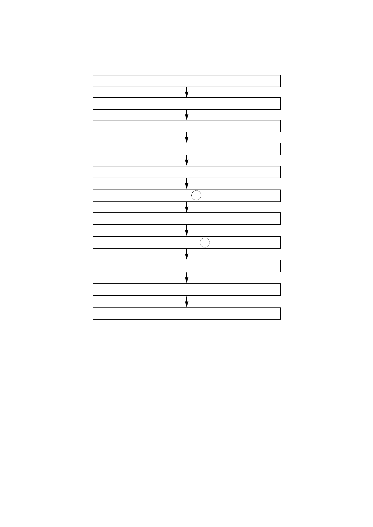
TROUBLESHOOTING GUIDE
1. Initial Lead-in Operation
Reset or Power-On.
LED Flickers.
Pick-Up moves to the inner-Track.
Laser on the Pick-Up lights.
Focus Search (through moving up and down the lens of Pick-Up)
Focus Servo On (FEO(IC501 Pin 12 ) signal generation)
Rotate disc.
Tracking Servo On (TEO (IC501 Pin 15 ) Signal generation)
Spindle Servo On (DMSO(TP25) Signal generation)
Read TOC Area (LED Flickers)
Search the Start of Data Area and then pause.
Page 3
21
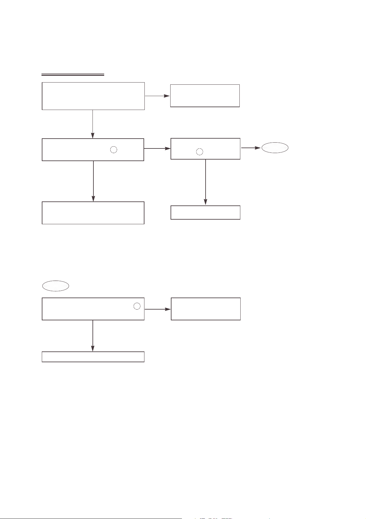
3. Troubleshooting Guide
A. LED doesn’t light.
Check Power Voltage (TP1:3.3V, TP2:12V)
Reference Voltage
[TP5:V13(1.3V) and GND.]
Does “H” output in IC501 pin ?
Check and replace R705, R706, Q701
and LED701 (LED703 for DELL).
Is the CLOCK Frequency of
IC501 pin 33.86MHz?
Check the power input
pattern.
Check IC501.
Check and replace
X501; 33.86MHz.
Is the CLOCK Frequency of IC501 pin
33.86MHz?
Check and replace IC501.
YES
OK
NG
YES
YES
NO
NO
NO
37
54
54
A-1
A-1
Page 4
22
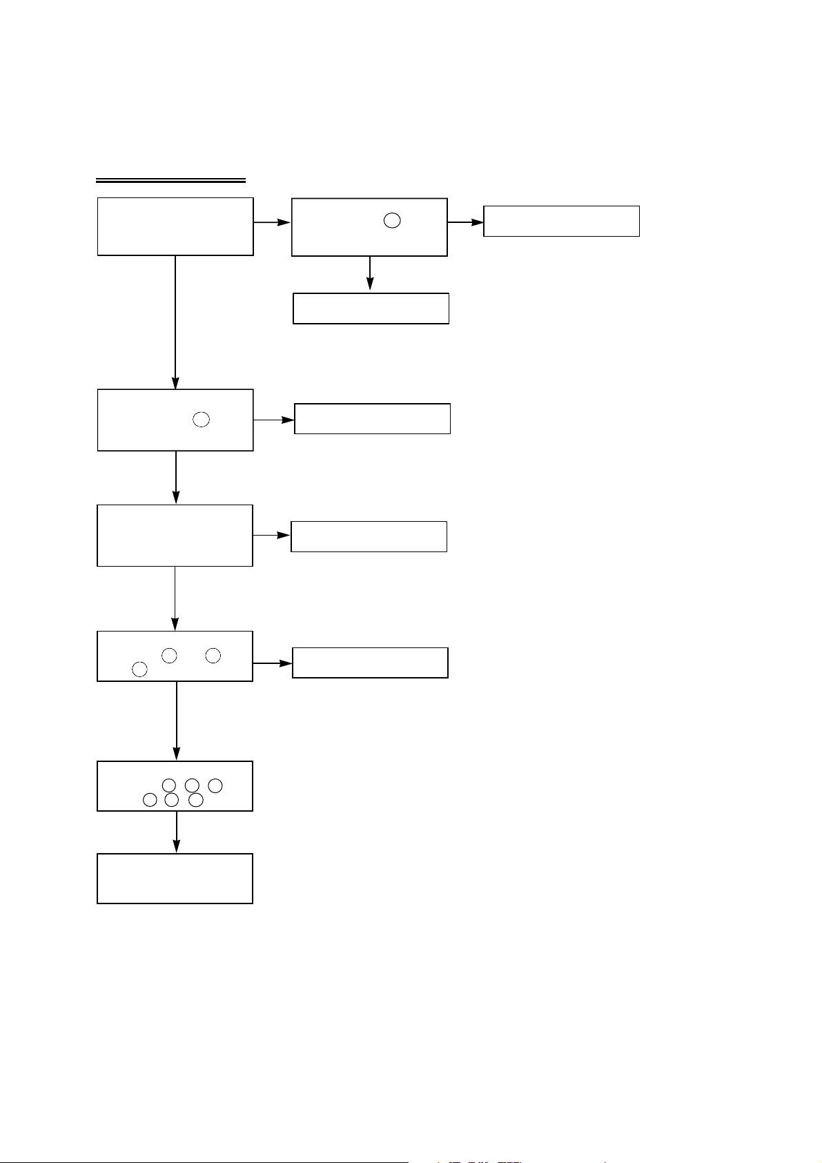
B. Pick-Up doesn’t move to the inner track.
Do the signals appear at IC501
pin , ?
(Refer to Fig. B-1.)
Do the signals appear in PN301
pin?
(Refer to Fig. B-2.)
Does “H” output at IC201
pin ?
Is the 1.3V at IC201 pin ?
Check the pattern from
IC501 pin to IC201
pin
.
Check IC501.
Check IC501.
Check the PN301, and then
replace the Sled Motor.
YES
YES
YES
YES
NO
NO
Replace IC201.
NO
NO
173
41
25
174
165
41
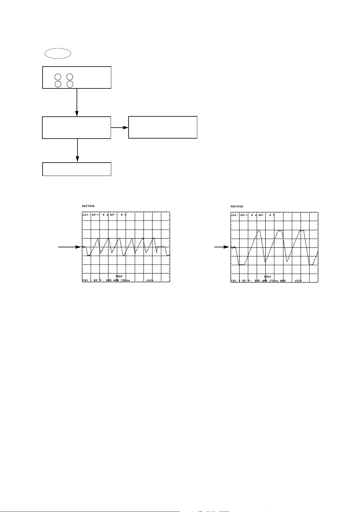
CH1
PIN174
FMO
CH2
PIN173
FMO2
CH1 TP4
CH2 TP5
CH3 TP6
CH4 TP7
Fig. B-1. FMO and FMO2 Signals
Fig. B-2. TP4, TP5, TP6 and TP7 Signals
Page 5
Check the pattern from
IC501 pin to R225
and then replace IC501.
23
Is the voltage of IC501 pin
(LD0) 1V?
Check Pick-Up FFC, PN101.
Check Q101, C101, C102
and then replace IC101.
YES
NO
10
181
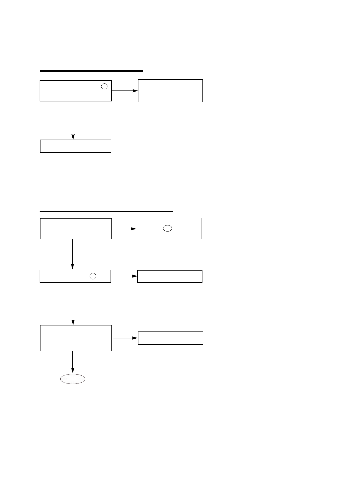
Does the focus search signal
appear at F0S0 (TP9)?
(Refer to Fig. D-1.)
Is the 1.3V at IC201 pin ?
Check IC501.
YES
YES
YES
NO
NO
Replace IC201.
NO
25
Does the focus search signal
appear between F+ (TP10)
and F- (TP11)?
(Refer to Fig. D-2.)
C. The Laser of Pick-Up doesn’t light.
D. The Pick-UP lens doesn’t move up and down.
D-1
Page 6
24
Check the pattern from
pin , of IC201 to
pin , of PN101.
Check the PN101, Pick-Up
FFC.
Replace the Pick-Up.
Replace PN101 or Pick-Up
FFC.
OK
OK
NG
34
35
1
4
CH1
TP9
(FAO)
CH1
TP10(F+)
TP11(F-)
Fig. D-1. F0S0 Signal
Fig. D-2. Focus Search Signal
D-1
Page 7
25
Does the signal appear at
the DMS0 (TP25)?
(Refer to Fig. E-3.)
Do the signals appear at
IC201 pin (W), (V),
and (U)?
Replace IC501.
Replace IC201.
YES
NO
NO
12
14
13
Check the pattern from
IC201 pin , , to
PN201 , , .
YES
OK
12
13
14
13
12
11
Check Spindle Motor FFC
and then replace the
Spindle Motor.
Does the signal appear at
FEO(IC501 pin ) when
the R126 opened?
(Refer to Fig. E-1.)
YES
YES
YES
NO
NO
Replace IC501.
Replace IC501.
Replace Pick-Up.
NO
Do the signal appear at
FEO (IC501 pin )?
(Refer to Fig. E-2.)
Does the signal appear at
F+(TP10) during focus
search?
E. Disc doesn’t rotate.
12
12
Page 8

26
Fig. E-2. FEO Signal
CH1
TP15:
FEO
Fig. E-3. DMS0 Signal
CH1
TP25:
DMS0
Fig. E-1. S-Curve
CH1
TP15:
S-Curve
Page 9

27
Is the Focus Servo ON?
(Does FEO(IC501 pin )
signal appear?)
Does A, B, C, D signal
appear at IC501 pin ,
?
YES
YES
NO
3
12
4
NO
Is the Tracking Servo ON?
(Does TEI (IC501 Pin )
signal appear?)
Does E, F signal appear
at IC501 pin , ?
YES
NO
8
YES
Is TOC area on the disc
read? (Does LED flicker?)
Does the other disc
operate normally?
Normal Disc is defective.
YES YES
NO
9
NO
Does RFAC signal (IC501
Pin ) appear?
Is Spindle Servo ON?
(Does DMS0 signal
(TP25) appear?)
YES YES
NO
NO
NO
Does RFI signal appear
at IC501 pin ?
1
20
Replace IC101.
Replace IC501.
Replace IC501.
Replace Main Circuit
Board or MD Ass’y.
NO
Refer to C.
(The Laser of Pick-Up
doesn’t light.)
F. TOC isn’t read.
15
Page 10

28
Does Audio signal appear
at IC501 pin , ?
(Refer to Fig. G-1.)
YES
NO
110 112
Replace IC501.
Does “H” signal appear at
IC501 pin ?
YES
NO
25
Check the IC501 pin
and then replace IC501?
108
Check C702.
YES
YES
YES
Are L-ch, R-ch signals
appear at JK701 and
Audio Line out connector
each?
NO
Check JK701 and
L701,L703.
Does Audio signal appear
at IC701 pin , ?
NO
1 7
Is the voltage of IC701
pin ?
6
NO
Replace IC701.
G. During Audio CD play, LED flickers, but Speaker is silent.
G-1
Page 11

29
Is the connection
between JK801 (or Audio
Line out connector) and
Line (or Jack) normal?
NO
Check the JK801 and
Audio line pattern.
YES
Check your sound card,
Audio Cable, Speaker,
Volume and Headphone
Jack.
Fig. G-1. Audio Signal
CH2
PIN3 of
IC601
CH2
PIN12 of
IC601
G-1
Page 12

4
1. CABINET
A. Release 3 screws (A).
B. Lift up the Cabinet in the direction of arrow (1).
(See Fig. 1)
2. MAIN CIRCUIT BOARD
A. Insert and press a rod in the Emergency Eject
Hole and then the CD Tray will open in the
direction of arrow (2).
B. Release 2 screws (B).
C. Remove the Main Circuit Board.
3. FRONT PANEL
A. Release 5 screws (C) and remove the Cover
Bottom.
B. Remove the Front Panel.
C. At this time, be careful not to damage the 5 hooks
(a) of the it.
4. BASE PICK-UP
A. Remove the Base Pick-Up.
(1)
(A)
(A)
(A)
Fig. 3
Fig. 1
Fig. 4
(B)
(B)
(2)
Fig. 2
DISASSEMBLY
CABINET
HOOKS
MAIN CIRCUIT BOARD
FRONT PANEL
ASSY
HOOK (a)
COVER
BOTTOM
BASE PICK-UP
EMERGENCY
EJECT HOLE
(C)
(C)
Page 13

8
AC
SUM
AC
VCA
EQ
APC
EQ_ON/OFF
RW/ROM
VC
DVC
RW/ROM
RW/ROM
RW/ROM
RW/ROM
RW/ROM
RW/ROM
(H/L)
DVcc
DVC
DVC
DVC
DVC
AVC
AVC
VOFST
VOFST
APC-OFF (Hi-Z)
B
C
A
D
VOFST
VC 2.5V
VC
DVC
AVC
-
+
-
+
-
+
-
+
-
+
-
+
-
+
DVcc
-
+
-
+
-
+
DVcc
DVcc
Vcc
Vcc
-
+
gm
gm
gm
++
6A7
B
SW
PD
LD
Vcc
GND
AVC
8C9
2
1
5
10
11
12
22 27
DVC
DVcc
14
14
CE20CEI
21
TE
18
TE_BAL19FE16FEI17RFDCO28RFDCI29DC_OFST30RFAC
VFC
4G
15
AC
25
RFC
26
BST
24
RFG
23
EQ_IN
3
AC_SUM
4
D
F
E
IC INTERNAL BLOCK DIAGRAM AND PIN DESCRIPTION
IC101 (CXA2581N) : RF Amplifier IC
I-V converts and amplifies the signal received from the pick-up and then applies to DSP part of onechip IC (IC501).
Block Diagram
Pin No.
Symbol I/O Description
1 LD O APC Amp Output
2 PD I APC Amp Input
3EQ-IN I Equalizer Input
4AC-SUM O
RF Summing Output of the RF AC Block
5 GND - GND
6 A I RF Input (A Signal)
7 B I RF Input (B Signal)
8 C I RF Input (C Signal)
9 D I RF Input (D Signal)
10 E I RF Input (E Signal)
11 F I RF Input (F Signal)
12 SW I Mode Switching Signal Input
13 DVcc I DVcc input
14 DVC O DVC output
15 RFAC O RFAC signal output
Pin Description
Pin No.
Symbol I/O Description
16 FE O Focus Error signal output
17 FEI - FE Amp Inverted
18 TE O Tracking Error signal output
19 TE_BAL I TE Balance Control
20 CE O Center Error Signal output
21 CEI - CE Amp Inverted
22 Vcc I Vcc
23 RFG I RFAC Low Frequency Gain Control
24 BST I EQ Boost Volume Control
25 VFC I EQ Cut off Frequency Control
26 RFC I EQ cut off Frequency Control
27 VC O VC output
28 RFDCO O RFDC Output
29 RFDCI - RFDC Amp inverted
30
DC_OFST
- RFDC OFF SET Control
Page 14

9
H1H
VDD
15kΩ
IN1
FB1
IN2
FB2
IN3
FB3
CT
VREF
STBY
0.012µF
1kΩ
1.1kΩ
H1L
16
44
25
14
H2H
H2L
13
12
H3H
H3L
VH
FG
FG Signal Output
Spindle Speed
Control Input
SFG
SBR
EC
ECR
VP
V
CL
SRESET
SSET
V
T
VN VO
GND
CS
RCS6
RCS5
RCS4
RCS3
RCS2
RCS1
A3
A22
A21
A1
VMSP2
VMSP1
BC2
BC1
11
10
9
7
6
50
18
17
19 20 21
40
51
3
4
53
54
55
1
52
8
49
37
38
VPUMP
39
PGSL
27
RO3
26
FO3
28
VMSL
22
PGAC
31
RO2
29
FO2
30
RO1
FO1
VMAC
32
35
36
15kΩ
20kΩ
20kΩ
20kΩ
0.012µF
0.012µF
100pF
1.65V
22µF
5V
47µF
100Ω
Rcs=
0.33Ω
5V
100µF
5V
47µF
0.1µF
0.1µF
100Ω
1kΩ
15kΩ
FF
Divide
Circuit
Hall
Comp
Matrix
5
56
2
H:active
L:standby
H:3FG
L:1FG
H:S-BRK
L:R-BRK
45
34
24
41
43
47
46
23
Absolute
value
S-BRK
Conversion
FG
Generator
Hall
Bias
+
X5
Upper
Drive
Low
Drive
DMOS
3-Phase
Bridge
OSC
Charge
Pump
DMOS
H/B
DMOS
H/B
DMOS
H/B
Drive
Logic
A
B
S
A
B
S
A
B
S
FB
FB
FB
Logic
Logic
Delta wave
Oscillator
VREF Reset
Stand-by
VDD Reset
Heat
Protection
Drive
Drive
M
IC201 (AN8498SH) : Servo Actuator Drive IC
Generates the signal to drive Focus Actuator Coil, Tracking Actuator Coil, Sled Motor, and Stepping
Motor by Control Signal input from DSP and u-COM.
Block Diagram
Page 15

10
Pin No
Symbol Description
1 A22 SP Drive Output 2
2 RCS6 SP Power Source 6
3 RCS5 SP Power Source 5
4 RCS4 SP Power Source 4
5 A3 SP Drive output 3
6 SFG SP FG mode conversion
7 FG SP FG signal output
8 VMSP2 SP Motor power supply 2
9 VH SP Hall Bias
10 H3L SP Hall (-) input 3
11 H3H SP Hall (+) input 3
12 H2L SP Hall (-) input 2
13 H2H SP Hall (+) input 2
14 H1L SP Hall (-) input 1
15 N.C. N.C.
16 H1H SP Hall + input 1
17 ECR SP Torque Reference input
18 EC SP Torque input
19 VP Op amp Non-inverted input
20 VN Op amp inverted input
21 VO Op amp output
22 VMSL Ch3 power supply
23 IN3 Ch3 input
24 FB3 Ch3 feedback output
25 STBY Stand-by
26 RO3 Ch3 inverted output
27 PGSL Ch3 Power GND
28 FO3 Ch3 Non-inverted output
Pin Description
Pin No
Symbol Description
29 RO2 CH2 inverted Output
30 FO2 CH2 Non-inverted Output
31 PGAC CH1, 2 Power GND
32 RO1 CH1 Inverted Output
33 N.C. N.C.
34 CT 3 Delta-wave Output
35 FO1 Ch1 Non-inverted Output
36 VMAC Ch1, 2 Power Supply
37 BC2 Charge Pump Volume Connector2
38 BC1 Charge Pump Volume Connector1
39 VPUMP
Charge Pump Boost the Voltage of Output
40 GND GND
41 IN1 CH1 Input
42 N.C. N.C.
43 FBI CH1 Feedback Output
44 VDD Control Circuit Power Supply
45 VREF Reference Voltage Input
46 FB2 CH2 Feedback Output
47 IN2 CH2 Input
48 N.C. N.C.
49 VMSP1 SP Motor Power Supply
50 SBR SP Break mode conversion
51 CS SP Voltage Defected Output
52 A1 SP Drive Output1
53 RCS3 SP Power Source 3
54 RCS2 SP Power Source 2
55 RCS1 SP Power Source 1
56 A21 SP Drive Output 2
Page 16

11
IC401 (H8/3397) : µ-COM
Controls all Drive systems by input and output the Data from the peripheral IC.
IC501 (CXD3030R) : DSP+ATAPI DECODER+DRAM
1Mbits DRAM
CLOCK
GEN
DATA
processor
DMA SEQUENCER
ADDRESS GEN
(Serial I/F)
CLOCK
GEN
PRIORITY RESOLVER
Subcode
Deinterleave & ECC
MAIN DATA
ERROR CORRECTION
ATAPI REGISTERS
12byte PACKET FIFO
HOST
I/F
DESCRAMBLER
SYNC CONTROL
Sub CPU I/F
DRVSS
DRVDD
HDB0~F
110~113
115~118
120~123
125~128
HCS0,1
97~99
95,96
HA0~2
XHRD
XHWR
XHAC
HDRQ
HINT
XS16
REDY
0~7D
0~6A
DASP
XPDI
XHRS
94
93
107
103
100
101
106
102
105
104
DMA FIFO
Digital OUT
8fs
1bit DAC
Error
Correction
block
Subcode P~W
Processor
32K RAM
EFM
Timing Generator
Subcode Q
Processor
84~91
XRD
77~83
76
XWR
75
XCS
74
XTL1
XINT
70
XWAT
69
XTL2
PWM2N
PWM2P
SENS
FOK
PWM1N
143 135 134 130 131
PWM1P
MIRR
DFCT
COUT
142
OP Amp
DACSERVO DSP
Auto Sequencer
8 bit
A/D
OP Amp
Analog SW
SAO
TAO
FAO
BSSD
DOUT
DAC
I/F
CD-DSP
I/F
CPU Interface
FOK
MIRR
DFCT
XTLO XTLI
138 130
Digital PLL
ASY
Sync protector
PCO
V
DD
Vss
44
FILI
43
FILO
42
CLTV
45
ASYI
49
ASYO
50
WFCK
SCOR
60
27
RFDC
CE
TESEFE
VC
SQCK
62
SQSO
61
MDP
PWMI
ADIO
RFAC
47
CLV/CAV
Processor
SERVO BLOCK
DAC BLOCK
DATA BLOCK
12
13
33343536373839
5 4 3 2 58 14 57 56 63 10
Block Diagram
Page 17

12
IC501 CXD3030R
Pin Description
Pin No. Symbol I/O Description
1 AVS6 Analog GND
2 SAO O Analog DAC Analog Output of Slide Filter
3 TAO O Analog DAC Analog Output of Tracking Filter
4 FAO O Analog DAC Analog Output of Focus Filter
5 BSSD I Constant Current Input for DAC Analog of Servo Filter
6 AVD6 Analog Power Supply (2.5V)
7 VSIO0 Digital GND
8 RMUT O 1,0 Audio DAC, Rch Zero Detection Play
9 LMUT O 1,0 Audio DAC, Lch Zero Detection Play
10 DOUT O 1,0 Digital-Out Output
11 SSTP I Disc Inner Track Detection Signal Input
12 MDP O 1,Z,0 Control Output of Spindle Motor
13 PWMI I External Terminal Input of Spindle Motor
14 DFCT I/O 1,0 Defect Signal In/Output
15 ATSK I Pin for Anti-Shock. It set to “L” When is not used.
16 MNT0/XRAOF O 1,0 MNT0/XRAOF* Signal Output
17 MNT1/C2PO O 1,0 MNT1/C2PO* Signal Output
18 MNT2/XUGF O 1,0 MNT2/XUGF* Signal Output
19 MNT3/GTOP O 1,0 MNT3/GTOP* Signal Output
20 VDCO Digital Power Supply (2.5V)
21 XRST I System Reset “L” is reset
22 VSCO Digital GND
23 MTST1 I Test Pin Normally “L”
24 MTST0 I Test Pin Normally “L”
25 XPLCK/WDCK O 1,0 XPLCK/WDCK*/C2PO*/PWM4* Signal Output
26 VDIO0 Digital Power Supply (3.3V)
27 WFCK/LRCK O 1,0 WFCK/LRCK*/PWM2* Signal Output
28 RFCK/PCMD O 1,0 RFCK/PCMD*/PWM3* Signal Output
29 LOCK/BCK O 1,0 LOCK/BCK* Signal Output
30 AVD2 Analog Power Supply (2.5V)
31 IGEN I Resistor Connection Pin of Current Source Reference for OP Amp
32 AVS2 Analog GND
33 ADIO O Analog OP Amp Output
34 RFDC I RF Signal Input
35 CE I Center Servo Analog Input
36 TE I Tracking Error Signal Input
37 SE I Slide Error Input
Page 18

13
Pin No. Symbol I/O Description
38 FE I Focus Error Input
39 VC I Center voltage Input
40 VPCO1 O 1,Z,0 Output of VCO2 for wide-Band EFM PLL
41 VCTL I Input of VCO2 Control voltage for Wide-Band EFM PLL
42 FILO O Analog Filter Output for Master PLL (Slave = Digital PLL)
43 FILI I Filter Input for Master PLL
44 PCO O 1,Z,0 Change Pump Output for Master PLL
45 CLTV I Multiplier VCO Control Voltage Input
46 AVS1 Analog GND
47 RFAC I EFM Signal Input
48 BIAS I Asymmetry Circuit Constant Current Input
49 ASYI I Asymmetry Comparator Voltage Input
50 ASYO O 1,0 EFM Full-Swing Output (L=V
SS, H=VDD)
51 AVD1 Analog Power Supply (2.5V)
52 ADC1 Digital Power Supply (2.5V)
53 ADC2 Digital Power Supply (2.5V)
54 VSC1 Digital GND
55 VSC2 Digital GND
56 FOK I/O 1,0 Focus OK Signal IN/OUT
57 MIRR I/O 1,0 Mirror Signal IN/OUT
58 COUT I/O 1,0 Track Number Count Signal IN/OUT
59 GFS O 1,0 GFS Output
60 SCOR O 1,0 Outputs a high signal when either subcode S0 or S1 is detected
61 SQSO O 1,0 SubQ 80bit PCM Peck and Level Data 16bit Output
62 SQCK I SQSO Readout clock Input
63 SENS O 1,Z,0 SENS Output to Sub CPU
64 SCLK I Sens Serial Data Readout Clock Input
Set to high when not used.
65 MUTE I DSP Mute (High:ON, Low:OFF)
66 DRV
DD Internal DRAM Exclusive Power Supply
67 DRV
SS Internal DRAM Exclusive GND
68 F16M O 1,0 1/2 Division of XTLI
Not changes with variable pitch.
69 XWAT O 1,0 Wait Signal for Sub CPU Buffer Memory Access, Negative Logic
70 XINT O 1,Z,0 Interrupt Signal to Sub CPU, Negative Logic
71 VDIO1 Digital Power Supply (3.3V)
72 VSIO1 Digital Power Supply GND
73 VSIO2 Digital Power Supply GND
74 XCS I Chip Select Signal from Sub CPU, Negative Logic
Page 19

14
Pin No. Symbol I/O Description
75 XWR I Data Write Strobe Signal from Sub CPU, Negative Logic
76 XRD I Data Read Strobe Signal from Sub CPU, Negative Logic
77 A6 I Sub CPU Address (MSB)
78 A5 I Sub CPU Address
79 A4 I Sub CPU Address
80 A3 I Sub CPU Address
81 A2 I Sub CPU Address
82 A1 I Sub CPU Address
83 A0 I Sub CPU Address (LSB)
84 D7 I/O 1,Z,0 Sub CPU Data Bus
85 D6 I/O 1,Z,0 Sub CPU Data Bus
86 D5 I/O 1,Z,0 Sub CPU Data Bus
87 D4 I/O 1,Z,0 Sub CPU Data Bus
88 D3 I/O 1,Z,0 Sub CPU Data Bus
89 D2 I/O 1,Z,0 Sub CPU Data Bus
90 D1 I/O 1,Z,0 Sub CPU Data Bus
91 D0 I/O 1,Z,0 Sub CPU Data Bus (LSB)
92 VDIO2 Digital Power Supply (3.3V)
93 XPDI I/O Z,0 Passed Diagnostics Signal, Open Drain Output, Negative Logic
94 DASP I/O Z,0 Drive Active/Slave Present Signal, Open Drain Output, Negative Logic
95 HCS1 I Chip Select Negative Signal from Host
96 HCS0 I Chip Select Negative Signal from Host
97 HA2 I Host Address (MSB)
98 HA0 I Host Address (LSB)
99 HA1 I Host Addresas
100 XS16 O Z,0 Host 16-bit I/O Port Select Signal, Open Drain Output, Negative Logic
101 HINT I/O 1,Z,0 Host Interrupt Demand Signal, Positive Logic
102 XHAC I DMA Acknowledge Signal from Host, Negative Logic
103 REDY O Z, 0 Host I/O Channel Ready Signal, Open Drain Output, Negative Logic
104 XHRD I Data Read Strobe Signal from Host
105 XHWR I Data Write Strobe Signal from Host
106 HDRQ O 1, Z, 0 DMA Request Signal to Host, Positive Logic
107 XHRS I Chip Reset Signal from Host, Negative Logic
108 VSIO3 Digital Power Supply GND
109 VDIO4 Digital Power Supply (3.3V)
110 HDBF I/O 1,Z,0 Host Data Bus (MSB)
111 HDB0 I/O 1,Z,0 Host Data Bus (LSB)
112 HDBE I/O 1,Z,0 Host Data Bus
113 HDB1 I/O 1,Z,0 Host Data Bus
Page 20

15
Notes :
• LRCK, BCK and PCMD are changed to 32-bit slot and 48-bit slot by command.
32-bit slot is output in 2's complements on an LSB-first basis and 48-bit slot is output in 2's complements on
an MSB-first basis.
• *'s signal is able to convert to output by a command. (Refer to sub CPU Register 08h (W) of decoder part)
• The GFS signal turns "H" upon coincidence between Frame Sync and the timing of interpolation protection.
• XRAOF is a signal issued when a jitter margin of + 28F is exceeded by the 32K RAM.
• C2PO is a signal to indicate data error.
Pin No. Symbol I/O Description
114 VSIO5 Digital Power Supply GND
115 HDBD I/O 1,Z,0 Host Data Bus
116 HDB2 I/O 1,Z,0 Host Data Bus
117 HDBC I/O 1,Z,0 Host Data Bus
118 HDB3 I/O 1,Z,0 Host Data Bus
119 VDIO3 Digital Power Supply (3.3V)
120 HDBB I/O 1,Z,0 Host Data Bus
121 HDB4 I/O 1,Z,0 Host Data Bus
122 HDBA I/O 1,Z,0 Host Data Bus
123 HDB5 I/O 1,Z,0 Host Data Bus
124 VSIO4 Digital Power Supply GND
125 HDB9 I/O 1,Z,0 Host Data Bus
126 HDB6 I/O 1,Z,0 Host Data Bus
127 HDB8 I/O 1,Z,0 Host Data Bus
128 HDB7 I/O 1,Z,0 Host Data Bus
129 VDC3 Digital Power Supply (2.5V)
130 XTL2 O 1, 0 Crystal Oscillating Circuit Output of the Clock for Decoder
131 XTL1 I Crystal Oscillating Circuit Input of the Clock for Decoder
132 VSC3 Digital GND
133 AVS3 Analog GND
134 PWM2N O 1, 0 PWM Output of Audio DAC. Default R Ch, Reverse Phase
135 PWM2P O 1, 0 PWM Output of Audio DAC. Default R Ch, Forward Phase
136 AVD3 Analog Power Supply (2.5V)
137 AVD4 Power Supply for Master Clock (2.5V)
138 XTLO O 1,0 Crystal Oscillating Circuit Output for the Master Clock
139 XTLI I Crystal Oscillating Circuit Input for the Master Clock
140 AVS4 GND for the Master Clock
141 AVS5 Analog GND
142 PWM1P O 1, 0 PWM Output of Audio DAC. L Ch, Forward Phase
143 PWM1N O 1, 0 PWM Output of Audio DAC. L Ch, Reverse Phase
144 AVD5 Analog Power Supply (2.5V)
Page 21

16
• XUGF is a negative Frame Sync pulse obtained from the EFM signal before Frame Sync protection is
effected.
• GTOP monitors the state of Frame Sync protection. ("H" : Sync protection window released)
• XPLCK is an inversion of the EFM PLL clock. The PLL is designed so that the falling edge of XPLCK
coincides with a change point of the EFM signal.
• RFCK is a signal generated at 136-µs periods using a crystal oscillator.
• LOCK is sampling the GFS at 460Hz and outputs "H" when GFS is "H".
("L" outputs when "L" is output eight times in succession or inputs when LKIN is "H".)
Page 22

A B C
1
2
3
4
24
BLOCK DIAGRAM
Spindle
motor
Drive
AN8498SH
RF
Amplifier
CXA2581N
Focus
actuator
Drive
Tracking
actuator
Drive
Slide
motor
Drive
AT-M08-0430
LPH-222A
Digital
Servo
Signal
Processor
CD-ROM
Decoder
&
Interface
System
Controller
HD643397S
CXD3030R
BH3525A
Digital
Signal
Processor
Audio
Signal
Processor
Audio
Amplifier
HOST COMPUTER
Optical
Pick-up
24C6989050
Spindle
motor
Slide motor
Page 23

A B CD
1
2
3
4
5
5
011
013
001
012
009
008
004
A01
005
PBM00(MAIN C.B.A)˚
428
428
428
428
428
435
435
006
A00
003
010
EXPLODED VIEW
 Loading...