

Page 1

3
INTRODUCTION
GENERAL FEATURE
SPECIFICATIONS
1. MODEL: CRD-8484B
1) SUPPORTED SYSTEM
• IBM Compatible 486SX or Above (With PIO mode 4 recommended)
2) SUPPORTED OS
3) GENERAL PERFORMANCE
• Data Transfer Rate .........................................................................................Sustained Data Transfer Rate
22Times Speed (Inner side) : 3,300 kbytes/sec
48 Times Speed (max., Outer side) : 7,200 kbytes/sec
• Data Buffer Capacity.....................................................................................................................128 kbytes
• Access Time.......................................................................................Random Access Time : 75 ms Typical
4) POWER REQUIREMENTS
• Voltage ......................................................................................................................................+5V DC +5%
+12V DC +5%
• Ripple ..................................................................................................................+5V : Less than 100mVp-p
+12V : Less than 100mVp-p
• Current .......................................................................................................................+5V : 0.9A (Maximum)
+12V : 1.5A (Maximum)
5) AUDIO PERFORMANCE
• Frequency Response.....................................................................................................20Hz~20KHz(+3dB)
• S/N Ratio (IHF-A+20 KHz LPF) .......................................................................75 dB (Typical at 1 KHz 0dB)
70 dB (Limit at 1 KHz 0dB)
• T.H.D. (IHF-A+20 KHz LPF)............................................................................0.05% (Typical at 1 KHz 0dB)
0.15% (Limit at 1 KHz 0dB)
• Channel Separation (IHF-A+20 KHz LPF).............................................................................75 dB (Typical)
70 dB (Limit)
• Output Voltage (1kHz 0dB) 47KΩ Load...............................................................................0.75Vrms + 10%
• Headphone Level (1kHz 0dB) 33Ω Load...............................................................................0.7Vrms + 20%
• Enhanced IDE interface
• Internal 5.25 inch, halfheight CD-ROM Drive
• Fast 75ms Average Access Time
• Max 7,200KB/sec Sustained Transfer rate
• Photo-CD Multisession Disc Spec compliant
• Multimedia MPC-3 Spec compliant
• Power Tray Loading/Ejection Mechanism
• 3 Way Eject support
(Software, O/C Button, Emergency Eject)
• Closed Enclosure
• Built-in ATAPI Interface Controller
• Software Volume Control
• 8 Times Digital Filter for CD Audio
• Built-in MODE-1 ECC/EDC
• MTBF 125,000h POH (at 10% Utilization)
• PIO Mode 4 & Multi DMA Mode 2 support
• Horizontal or Vertical Mounting
• Digital audio output connector
• Digital audio through ATAPI Interface
• Subcode (P-W) through ATAPI Interface
• Spin-down Mode for energy saving
• MS-DOS Version 3.1 or Higher
• Windows '95/'98/’2000
• Solaris Ver 2.4 or Higher
• Linux slackware Ver 2.3
• Windows NT 4.0 or later
• OS/2 Warp (Ver 3.0)
This service manual provides a variety of service
information. It contains the mechanical structure of
the CD-ROM Drive together with mechanical
adjustments and the electronic circuits in schematic
form. This CD-ROM Drive was manufactured and
assembled under our strict quality control standards
and meets or exceeds industry specifications and
standards.
Page 2
2. Trouble List (Circuit)
A. LED doesn’t light.
B. Pick-Up doesn’t move to the inner-track.
C. The Laser of Pick-Up doesn’t light.
D. Pick-Up lens doesn’t move up and down.
E. Disc doesn’t rotate.
F. TOC isn’t read. (The LED turns on, but doesn’t flicker.)
G. During Audio CD Play, LED flickers, but Speaker is silent.
23
TROUBLESHOOTING GUIDE
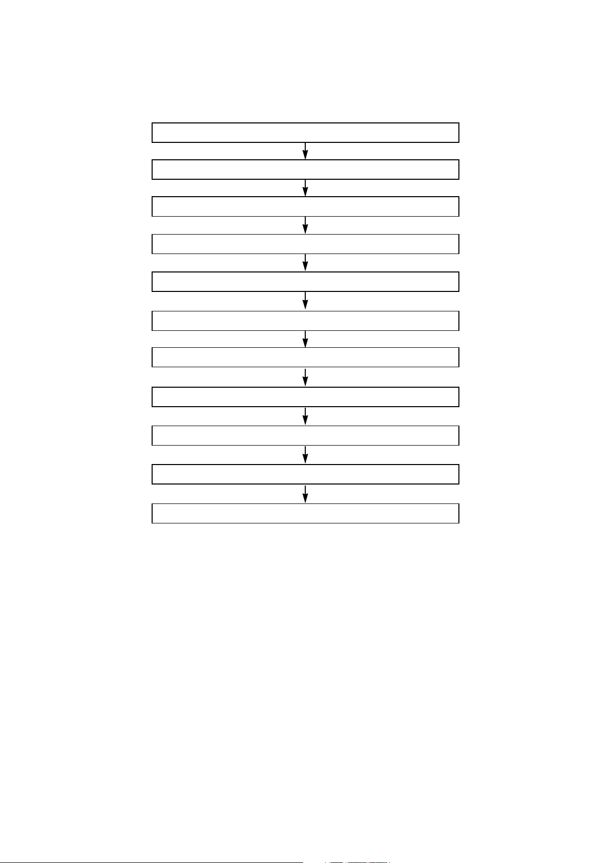
1. Initial Lead-in Operation
Reset or Power-On.
LED Flickers.
Pick-Up moves to the inner-Track.
Laser on the Pick-Up lights.
Focus Search (through moving up and down the lens of Pick-Up)
Focus Servo On (FEO(TP15) signal generation)
Rotate disc.
Tracking Servo On (TEO(TP14) Signal generation)
Spindle Servo On (SPO(TP25) Signal generation)
Read TOC Area (LED Flickers)
Search the Start of Data Area and then pause.
Page 3
24
3. Troubleshooting Guide
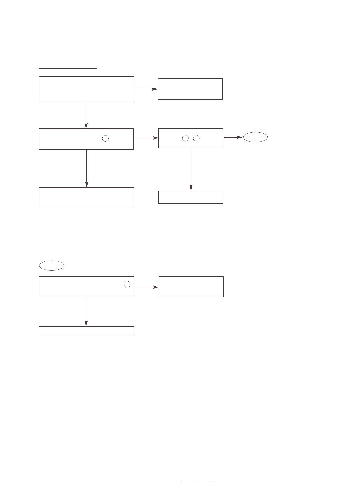
A. LED doesn’t light.
Check Power Voltage (TP1:3.3V, TP2:12V)
Reference Voltage
[TP3:VC(2.5V) and GND.]
Does “H” output in IC501 pin ?
Check and replace R105, R106, Q12
and LED701 (LED702 for NECCI).
Is the CLOCK Frequency of
IC501 pin ,
33.86MHz?
Check the power input
pattern.
Check IC501.
Check and replace X10;
33.86MHz.
Is the CLOCK Frequency of IC501 pin
33.86MHz?
Check and replace IC501.
YES
OK
NG
YES
YES
NO
NO
NO
170
93
94
54
A-1
A-1
Page 4

25
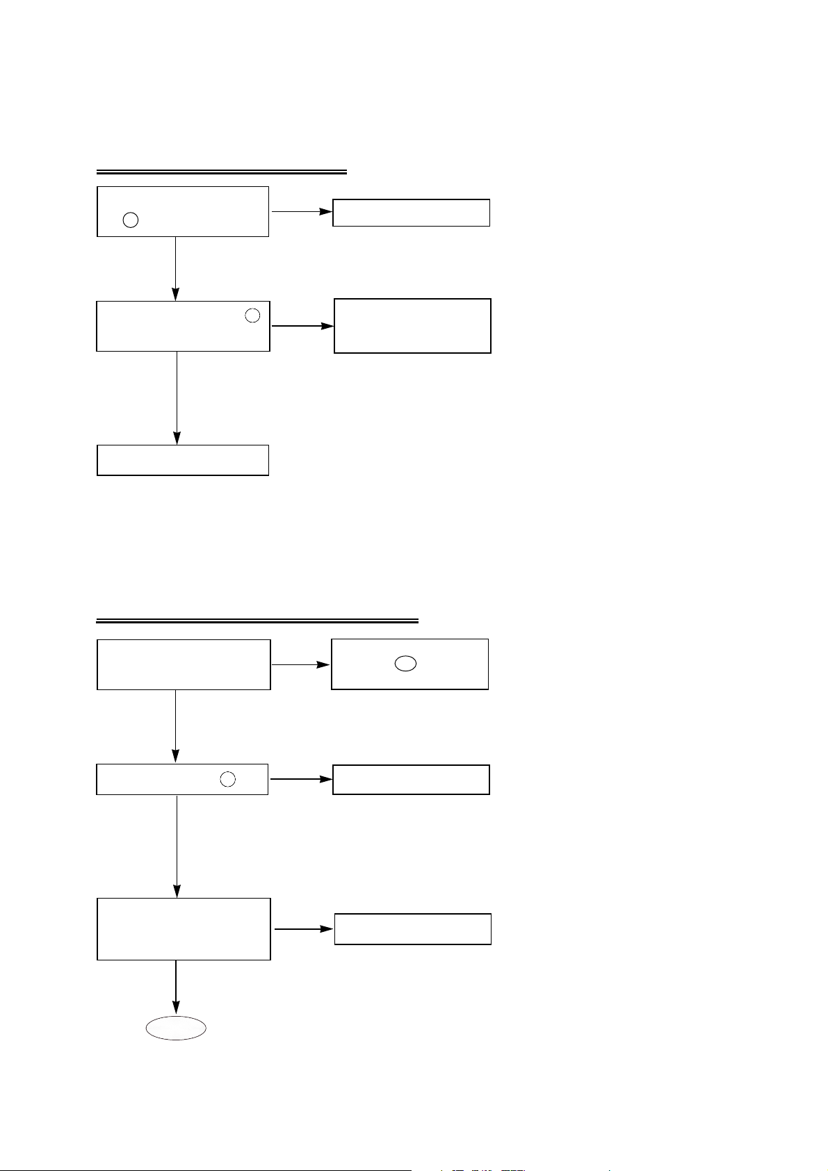
B. Pick-Up doesn’t move to the inner track.
Do the signals appear at IC501
pin , ?
(Refer to Fig. B-1.)
Do the signals appear in PN301
pin?
(Refer to Fig. B-2.)
Does “H” output at IC201
pin ?
Is the 2.5V at IC201 pin ?
Check the pattern from
IC501 pin to IC201
pin
.
Check IC501.
Replace IC102.
Check the PN301, and then
replace the Sled Motor.
YES
YES
YES
YES
NO
NO
Replace IC201.
NO
NO
34
41
25
35
107
41
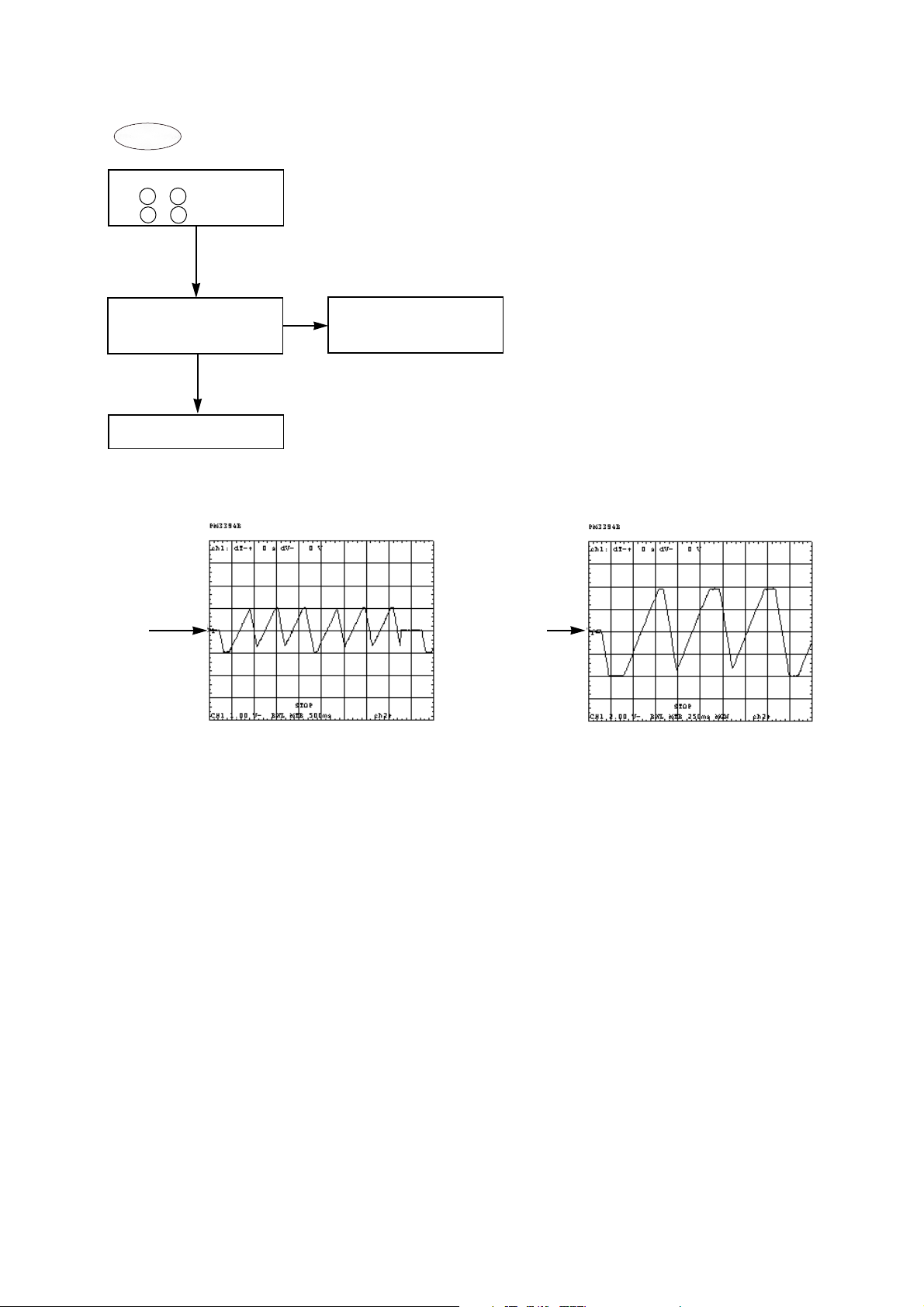
CH1
PIN34
DA0
CH2
PIN35
DA1
CH1 TP4
(/A)
(A)
(/B)
(B)
CH2 TP5
CH3 TP6
CH4 TP7
Fig. B-1. DA0 and DA1 Signals
Fig. B-2. TP4, TP5, TP6 and TP7 Signals
Page 5
Check the pattern from
IC501 pin to R42
and then replace IC501.
26
Does “Low” output at IC102
pin ?
Is the voltage of IC102 pin
(LDD) 2V?
Check Pick-Up FFC, PN101.
Check Q10, C10, C32,
R113, R114 and then
replace IC102.
Replace IC501.
YES
YES
NO
NO
13
157
15
Does the focus search signal
appear at FDO (TP9)?
(Refer to Fig. D-1.)
Is the 2.5V at IC201 pin ?
Replace IC102.
YES
YES
YES
NO
NO
Replace IC201.
NO
25
Does the focus search signal
appear between F+ (TP10)
and F- (TP11)?
(Refer to Fig. D-2.)
C. The Laser of Pick-Up doesn’t light.
D. The Pick-UP lens doesn’t move up and down.
D-1
Page 6
27
Check the pattern from
pin , of IC201 to
pin , of PN101.
Check the PN101, Pick-Up
FFC.
Replace the Pick-Up.
Replace PN101 or Pick-Up
FFC.
OK
OK
NG
34
35
1
4
CH1
TP9
(FDO)
CH1
TP10(F+)
TP11(F-)
Fig. D-1. FDO Signal
Fig. D-2. Focus Search Signal
D-1
Page 7
28
Does the signal appear at
the SP0 (TP25)?
(Refer to Fig. E-3.)
Do the signals appear at
IC201 pin (W), (V),
and (U)?
Replace IC501.
Replace IC201.
YES
NO
NO
12
14
13
Check the pattern from
IC201 pin , , to
PN201 , , .
YES
OK
12
13
14
13
12
11
Check Spindle Motor FFC
and then replace the
Spindle Motor.
Does the signal appear at
FEO (TP15) when the
IC501 pin opened?
(Refer to Fig. E-1.)
YES
YES
YES
NO
NO
Replace IC501.
Replace IC501.
Replace Pick-Up.
NO
Do the signal appear at
TP15 (FEO)?
(Refer to Fig. E-2.)
Does the signal appear at
F+(TP10) during focus
search?
E. Disc doesn’t rotate.
144
Page 8

29
Fig. E-2. FEO Signal
CH1
TP15:
FEO
Fig. E-3. SPO Signal
CH1
TP25:
SPO
Fig. E-1. S-Curve
CH1
TP15:
S-Curve
Page 9

30
Is the Focus Servo ON?
(Does FEO (TP15) signal
appear?)
Does A, B, C, D signal
appear at IC102 pin ,
?
YES
YES
NO
7
8
NO
Is the Tracking Servo ON?
(Does TEO (TP14) signal
appear?)
Does E, F signal appear
at IC102 pin , ?
YES
NO
9
YES
Is TOC area on the disc
read? (Does LED flicker?)
Does the other disc
operate normally?
Normal Disc is defective.
YES YES
NO
10
NO
Does RFI signal appear?
Is Spindle Servo ON?
(Does SP0 signal (TP25)
appear?)
YES YES
NO
NO
NO
Does RFIN signal appear
at IC102 pin ?
6
Replace IC102.
Replace IC102.
Replace IC501.
Replace Main Circuit
Board or MD Ass’y.
NO
Refer to C.
(The Laser of Pick-Up
doesn’t light.)
F. TOC isn’t read.
Page 10

31
Does Audio signal appear
at IC501 pin , ?
(Refer to Fig. G-1.)
YES
NO
87 90
Replace IC501.
Does “H” signal appear at
IC501 pin ?
YES
NO
113
Check the IC501 pin
and then replace IC501?
113
Check C87.
YES
YES
YES
Are L-ch, R-ch signals
appear at JK701 and
Audio Line out connector
each?
NO
Check JK701 and
L701,L703.
Does Audio signal appear
at IC602 pin , ?
NO
1 7
Is the voltage of IC602
pin 2.5V?
6
NO
Replace IC602.
G. During Audio CD play, LED flickers, but Speaker is silent.
G-1
Page 11

32
Is the connection
between JK801 (or Audio
Line out connector) and
Line (or Jack) normal?
NO
Check the JK801 and
Audio line pattern.
YES
Check your sound card,
Audio Cable, Speaker,
Volume and Headphone
Jack.
Fig. G-1. Audio Signal
CH1
PIN87 of
IC501
CH2
PIN90 of
IC501
G-1
Page 12

1. CABINET and CIRCUIT BOARD
DISASSEMBLY
1-1. Bottom Chassis
A. Release 4 screws (A) and remove the Bottom
Chassis in the direction of arrow (1). (See Fig. 1-1)
1-2. Front Bezel Assy
A. Insert and Press a rod in the Emergency Eject
Hole and then the CD Tray will open in the
direction of arrow (2).
B. Remove the Tray Door in the direction of arrow (3)
by pushing it outward.
C. Release 3 stoppers and remove the Front Bezel
Assy.
1-3. Cabinet and Main Circuit Board
A. Remove the Cabinet in the direction of arrow (4).
(See Fig. 1-3)
B. Release 2 hooks (a) and remove the CD Tray.
C. Remove the Soldering of the LD- and LD+ (B) for
the Loading Motor, and then remove the Main
Circuit Board.
D. At this time, be careful not to damage the 3
connectors of the Main Circuit Board.
2. MECHANISM ASSY
A. Separate the Pick-Up Unit from the Mechanism
Assy.
B. Release 1 screws (C) and then remove the Pick-
Up ( ).
DISASSEMBLY
(A)
(A)
(A)
(A)
(1)
Bottom Chassis
Fig. 1-1
Fig. 1-2
Fig. 1-3
Fig. 1-4
5
Cabinet
(4)
Hooks (a)
(B)
Main
Circuit Board
Tray Door
(3)
Stoppers
Emergency Eject Hole
(2)
Front Bezel Assy
CD Tray
Pick-up Unit
(C)
Mechanism Assy
Page 13

13
PHOTO DIODE STRUCTURE OF THE PICK-UP
(1) Focus Error Signal –> (A+C)-(B+D)
(Control the Pick-up’s up and down to focus on the Disc)
(2) Tracking Error Signal –> (E-F)
(Control the Pick-up’s left and right shift to find the track on the Disc)
(3) RF Signal –> (A+B+C+D)
(
RF Signal is converted to Data Signal in One Chip IC (IC501))
Three signals (Focus Error Signal, Tracking Error Signal and RF Signal) above are I-V converted and
amplified at the IC102, and then are transmitted to One Chip IC (IC501) to generate the Servo Control
Signal and Data Signal.
Red laser
Pick-Up module
Tracking
Focusing
B
C
E
F
D
A
Page 14

14
REF
REFREF
REF
REF
REF
REF
REF
REF
REF
REF
REF
REF
REF
REF
VCC
VCC
VCC
APC
PH
PH
EQ-CONTROL
BH
BH
PH-CONTROL
7_MODE
5V
39K
33K
52
5V
+
7_MODE
36
PH
100K
1
2
3
4
5
6
7
BHC
PHC
RFAO
GND1
RFA-
RFIN
FIN1
35
BH
34
VCC1
33
RFSM
32
RHLD
31
GND2
30
REFL
29
FE-
28
FE
27
TE-
26
TE
25
TSS
24
TS
23
VCC2
22
TSH
21
FBAL
20
TBAL
19
SGC
100K
8
FIN2
56K
9
E
F
VCC
56K
10
11
12
REFI
VREF
13
LDD
14
LDS
15
LDON
16
GHS
17
BHH
18
EQS
IC INTERNAL BLOCK DIAGRAM AND PIN DESCRIPTION
• IC102 (LA9246T) : RF Amplifier IC
I-V converts and amplifies the signal received from the pick-up and then applies to DSP part of onechip IC (IC501).
Block Diagram
Page 15

15
Pin No. Pin Name Descriptions
1 BHC Bottom hold external condensor pin for checking RFAGC.
2 PHC Peak hold external condensor pin for checking RFAGC.
3 RFAO RF Pre AMP output
4 GND RF GND
5 RFA- RF Pre AMP (-) input
6 RFIN RF Sum input
7 FIN1 Pickup output (B+D),
8 Fin2 Pickup output (A+C),
9 E Pickup output (E)
10 F Pickup output (F)
11 REFI Eeternal Condensor Pin of Reference Voltage.
12 VREF Reference output
13 LDD APC circuit output
14 LDS APC circuit input
15 LDON Laser on/off.
16 GHS RF signal gain control.
17 BHH BH response control.
18 EQS RF equalizer. PH detection control
19 SGC Servo gain control
20 TBAL TE balance adjust
21 FBAL FE balance adjust
22 TSH TS wide band control
23 VCC2 Servo VCC
24 TS TS output
25 TSS TS wide band control
26 TE TE signal output (To DSP)
27 TE- TE gain control
28 FE FE signal output (To DSP)
29 FE- FE gain control
30 REFL Reflection output (To DSP)
31 GND2 Servo GND
32 RHLD RF hold control
33 RFSM EFM signal output (To DSP)
34 VCC1 RF VCC
35 BH RF bottom hold output (To DSP)
36 PH RF peak hold output (To DSP)
Pin Description
Page 16

16
• IC201 (M63022FP) : Drive IC (Spindle/Servo Actuator)
Rotates the Spindle Motor by receiving MDP signal from IC501.
Generates the signal to drive Focus Actuator Coil, Tracking Actuator Coil, Sled Motor, and Stepping
Motor by Control Signal input from DSP and u-COM.
Block Diagram
x12
x8
x12
FG
HU+
HUHV+
HV-
HW+
HWHB
SPIN
REF
SL1IN
SL2IN
FOIN
TOIN
5Vcc
TO+
TO-
FO+
FO-
GND
LO+
LO-
VM3
LOIN+
BRS
OSC
MU1
S
SS
S
VM1
RSPUV
W
RSL1
RSL2
SL1+
SL1-
SL2+
SL2-
VM2
FG
Reverse
Detect
120ß
MATRIX
Hall Bias
CTL
amp
Direction
comp
Direction
comp
Direction
comp
Current
comp
Current
comp
Current
comp
CTL
amp
CTL
amp
Logic
Logic
TSD
BIAS
Frequency
generator
VM1
Regulator
Reg
Pin Description
Pin No.
Symbol Description
Pin No.
Symbol Description
1 SL1IN Slide control voltage input 1
2 SL2IN Slide control voltage input 2
3 VM2 Motor Power Supply 3 (for Slide)
4 RSL2 Slide current sense 2
5 SL2+ Slide non-inverted output 2
6 SL2- Slide inverted output 2
7 GND GND
8 RSL1 Slide current sense 1
9 SL1+ Slide non-inverted output 1
10 SL1- Slide inverted output 1
11 GND GND
12 W Motor drive output W
13 V Motor drive output V
14 U Motor drive output U
15 RSP Spindle current sensie
16 HW- HW- sensor amp. input
17 HW+ HW+ sensor amp. input
18 HV- HV- sensor amp. input
19 HV+ HV+ sensor amp. input
20 HU- HU- sensor amp. input
21 HU+ HU+ sensor amp. input
22 VM1 Motor Power Supply 1 (for Spindle)
23 HB Bias for Hall Sensor
24 FG Frequency generator output
25 REF Refernce voltage input
26 SPIN Spindle control voltage input
27 FOIN Focus control voltage input
28 TOIN Tracking control voltage input
29 GND GND
30 5VCC 5V Power Supply (for FS, TS)
31 TO- Tracking inverted output
32 TO+ Tracking non-inverted output
33 GND GND
34 FO+ Focus non-inverted output
35 FO- Focus inverted output
36 LO+ Loading non-inverted output
37 LO- Loading inverted output
38 BRS Brake select control terminal
39 VM3 Motor power supply 3.(for Loading)
40 LOIN+ Loading control input( +)
41 MU1 Mute 1
42 OSC PWM carrier oscilation set
Page 17

Driver
VCEC
PLL
TDO, FDO
SLDO, SPDO
*11
*1
*12
*2
*14
*3
*4
*5
*6
LA9238
CD-DSP
Data bus[0.7]
DRAM
Data bus[0.15]
LC895300
LC895299
Adress bus[0.18]
Sub-code I/F
de-interleve
Adress generator
Sub-code ECC
Address generator
Address generator
Address generator
Address generator
Address generator
ATAPI I/F
Data output input I/F
Microcontroller
RAM access
De-scramble &
Buffering
ECC & EDC
SRAM
CD-DSP I/F
& SYNC
Detector
Merge
EXT10
CMDI
Each Block
Register
FGCNT
Audio
Circuit
ZRESET
HOST
decoder
*7
*8
*10
*9
*13
XTALCK
Each Block
XTAL
Micro
controller
1.5K
RAM
Clock
generator
Buffer
DRAM
Bus
Arbiter
&
DRAM
controller
Each Block
Bus control
siganl
128K
EEPROM
A0~A16
D0~D7
ZOE, ZWE, ZCE
Gray Block si characteristic of LG895300.
Interrupt
Controller
Timer
FGCNT CMDI
EXTII
SW1
SW2
SW3
IOPORT
0~14
FG
17
• IC501 (HMS895300) : DSP+ATAPI DECODER+DRAM + µ-COM
Block Diagram
*1 EFMIN,EFMIN2,PH,BH,FE,TE,TES,RREC
*2 RHLD,TSH,EQS,GHS,LDON,FBAL,TBAL,TOFST,SGC
*3 LOUT,ROUT,DOUT
*4 DD~DD15,ZDASP,ZPDIAG
*5 ZCSIFX,ZCS3FX,DA0~2,ZDIOR,ZDIOW,ZDMACK,ZHRST,CSEL
*6 DMARQ,HINTRQ,ZIOCS16,IORDY
*7 ZRD,ZWR,ZCS,MCK,SUA0~7
*8 D0~7
*9 CRCERR/FLOCK,HFLO/WRQ/DIR/TLOCK,FSEQ,FSX/LRCK/FV,EFLG/ CK2/PRF,C2F/PCK,EFMOUT
*10 TEST0~2
*11 PCKISTF,PCKIFTP,PDO,POS1~3,RF
*12 SLCO0~3,JITC,DSLB,PHC,BHC
*13 PLL1
*14 SLCIT1~2,AD1,VREF,CSS
Page 18

18
• IC501 HMS895300
Pin Description
Pin No. Signal Type COMMENT
1 Vss P Logic GND
2 A11 O PROM ADDRESS
3A9 O
4A8 O
5 A13 O
6 A14 O
7 Wstrobe O Write Strobe
8 A16 O 128K
9 A15 O 64K
10 A12 O
11 A7 O
12 A6 O
13 A5 O
14 A4 O
15 A3 O
16 A2 O
17 A1 O
18 A0 O
19 DATA0 B PROM DATA
20 DATA1 B
21 VDDD P DRAM VDD 5V
22 VDD1 P 3.3V
23 Vss P Logic GND
24 VSSD P DRAM GND
25 DATA2 B PROM DATA
26 DATA3 B
27 DATA4 B
28 DATA5 B
29 DATA6 B
30 DATA7 B
31 ZCE O Chip Enable Signal
32 A10 O PROM ADDRESS
33 Psen O Access Enable Signal
34 IOPORT0 B General Input/Output Port
35 IOPORT1 B
36 IOPORT2 B
TYPE
I:INPUT B:BIDIRECTION NC:NOT CONNECT O:OUTPUT P:POWER
Page 19

19
Pin No. Siganl Type COMMENT
37 TEST0 I TEST PIN (GND)
38 WRQ/HFLO/DIR/TLOCK O Monitor Pin
39 FSEQ/DEF O Frame Sync/DEFECT
40 DOUT/TESO O Digital OUT
41 VDD0 P I/O 5V power supply
42 VSS P Logic GND
43 PLL1 O System Clock PLL
44 PLL1VDD P Logic PLL VDD 3.3V
45 PLL1VSS
P logic PLL GND
46 CSEL I ATAPI I/F
47 ZHRST I
48 ZDASP B
49 ZCS3FX I
50 ZCS1FX I
51 Vss1 P I/F GND
52 VDD0 P I/O 5V power supply.
53 DA2 I ATAPI I/F
54 DA0 I
55 ZPDIAG B
56 DA1 I
57 ZIOCS16 O
58 Vss1 P I/F GND
59 HINTRQ O ATAPI I/F
60 ZDMACK I
61 IORDY O
62 ZDIOR I
63 ZDIOW I
64 DMARQ O
65 VDD0 P I/O 5V power supply.
66 VDD1 P 3.3V
67 Vss1 P I/F GND
68 DD15 B ATAPI I/F
69 DD0 B
70 DD14 B
72 DD13 B
73 DD2 B
74 DD12 B
75 DD3 B
76 Vss
1 P I/F GND
Page 20

20
Pin No. Siganl Type COMMENT
77 DD11 B ATAPI I/F
78 DD4 B
79 DD10 B
80 DD5 B
81 DD9 B
82 DD6 B
83 DD8 B
84 DD7 B
85 VDD0 P I/O power supply 5V
86 TEST1 I TEST Pin (GND)
87 ROUT O DAC output
88 AUVDD P DAC VDD 5V
89 AUVss P DAC GND
90 LOUT O DAC output
91 Vss P Logic GND
92 XTALCK I XTALCK input
93 XTAL O XTALCK output
94 VDD0 P I/O power supply 5V
95 FSX/LRCK O Monitor port
96 EFLG/CK2 O
97 TRV2/DATA B General input/output port
98 TRV B
99 FLOCK/CRCERR O FLOCK/CRCERR/C2F/PCK output
C2F/PCK
100 EFMOUT O EFM output
101 OUTPORT O General output port
102 SW1 I Tray Close
103 SW2 I Tray open
104 SW3 I Eject Switch
105 IOPORT3 B General input/output port
106 IOPORT4 B
107 IOPORT5 B
108 IOPORT6 B
109 VSSD P DRAM GND
110 VDD1 P 3.3V
111 Vss P logic GND
112 VDDD P DRAM VDD 5V
113 IOPORT7 B General input/output port
114 IOPORT8 B
Page 21

21
Pin No. Siganl Type COMMENT
115 IOPORT9 B General input/output port
116 DSLB O SLC PWM output
117 AVDD P Slice Level VDD 3.3V
118 SLCIST1 I EFM Slice Level Control port
119 SLCIST2 I
120 SLCO0 O EFM Slice level output
121 SLCO1 O
122 SLCO2 O
123 SLCO3 O
124 EFMIN I EFM input pin
125 EFMIN2 I
126 AVss P Slice Level GND
127 JITC O Jitter output
128 PWM0 I VCO PWM output
129 FR I VCO frequency control port
130 PCKISTF I Frequency comparater charge pump control port
131 PCKISTP I Phase comparater charge pump control port
132 PLL2VDD P VCEC PLL VDD 3.3V
133 PLL2Vss P VCEC PLL GND
134 PDO O Charge Pump Filter
135 PDS1 O Charge Pump select port
136 PDS2 O
137 PDS3 O
138 RPO O P/N Balance Adjust port
139 SVss P Servo GND
140 AD1 I AD input1
141 PH I Peak HOLD
142 BH I Bottom HOLD
143 RREC I Optical judge input port
144 FE I FE input port
145 TE I TE input port
146 TES I TES compartor input
147 VREF I VREF input port
148 PHC O PH Slice condensor input port
149 BHC O BH Slice condensor input port
150 FBAL O Focus Balance port
151 TBAL O Tracking Balance Port
152 SGC O Servo gain control port
153 TOFST O Tracking offset Adjust port
Page 22

22
Pin No. Siganl Type COMMENT
154 SVDD P Servo VDD 5V
155 SVss P Servo GND
156 TDO O Tracking output
157 FDO O Focus output
158 SLDO O Sled output
159 SPDO O Spindle output
160 VDD0 P A/D & D/A 5V
161 Vss P Logic GND
162 VDD1 P 3.3V
163 RHLD O RFAGC hold output port
164 TSH O TS select port
165 EQS O RF Equalizer select port
166 GHS O RF signnal , TS signal gain
167 LDON O Laser Control port
168 TEST2 I TEST PIN (GND)
169 FG I FG input
170 IOPORT10 B General Input/output port
171 IOPORT11 B
172 IOPORT12 B
173 IOPORT13(Debug1) B Audio Mute
174 IOPORT14(Debug2) B LED Drive port
175 ZRESET I CHIP RESET
176 V
DD0 P I/O power supply 5V
Page 23

A B CD
1
2
3
4
5
+5V
+3.3V3.3V Reg.
M63022FP
LA9246T
HMS895300
FLASH
MEMORY
RF Amp.
DSP+Decoder+DRAM
+System controller
SPINDLE
MOTOR
FOCUS
COIL
SLED
MOTOR
LOADING
MOTOR
33.86MHz
I/F Cable
R-ch
L-ch
Line-out
H
O
S
T
TRACKING
COIL
Disc
Motor unit
Optical
Pick-up
MOTOR DRIVE
GND
GND
+12V
+5V
GND
GND
+12V
34
BLOCK DIAGRAM
* MODEL: CRD-8484B
Page 24

PBM00 (MAIN C.B.A)
PBF00 (FRONT C.B.A)
007
002
003
030
020
A02
A01
020
051
028
050
029
434
021
434
434
413
413
413
001
413
430
028
027
026
025
033
435
010
009
008
011
012
005
034
014
013
434
031
016
015
004
006
431
A B C D E F GH
1
2
3
4
5
EXPLODED VIEW
7
8
 Loading...