

Page 1

3
INTRODUCTION
GENERAL FEATURE
SPECIFICATIONS
1. MODEL: CRD-8481B
1) SUPPORTED SYSTEM
• IBM Compatible 486SX or Above (With PIO mode 4 recommended)
2) SUPPORTED OS
3) GENERAL PERFORMANCE
• Data Transfer Rate .........................................................................................Sustained Data Transfer Rate
20Times Speed (Inner side) : 3,000 kbytes/sec
48 Times Speed (max., Outer side) : 7,200 kbytes/sec
• Data Buffer Capacity.....................................................................................................................128 kbytes
• Access Time ...................................................................................................Random Access Time : 75 ms
4) POWER REQUIREMENTS
• Voltage ......................................................................................................................................+5V DC +5%
+12V DC +5%
• Ripple ..................................................................................................................+5V : Less than 100mVp-p
+12V : Less than 100mVp-p
• Current .......................................................................................................................+5V : 0.9A (Maximum)
+12V : 1.5A (Maximum)
5) AUDIO PERFORMANCE
• Frequency Response.....................................................................................................20Hz~20KHz(+3dB)
• S/N Ratio (IHF-A+20 KHz LPF) .......................................................................85 dB (Typical at 1 KHz 0dB)
80 dB (Limit at 1 KHz 0dB)
• T.H.D. (IHF-A+20 KHz LPF)............................................................................0.05% (Typical at 1 KHz 0dB)
0.15% (Limit at 1 KHz 0dB)
• Channel Separation (IHF-A+20 KHz LPF).............................................................................80 dB (Typical)
70 dB (Limit)
• Output Voltage (1kHz 0dB) 47KΩ Load.................................................................................0.7Vrms +10%
• Headphone Level (1kHz 0dB) 33Ω Load...............................................................................0.7Vrms +20%
• Enhanced IDE interface
• Internal 5.25 inch, halfheight CD-ROM Drive
• Fast 75ms Average Access Time
• Max 7,200KB/sec Sustained Transfer rate
• CRD-8481B: Max 7,200 KB/sec Sustained
Transfer rate
• CRD-8401B: Max 6,000 KB/sec Sustained
Transfer rate
• Photo-CD Multisession Disc Spec compliant
• Multimedia MPC-3 Spec compliant
• Power Tray Loading/Ejection Mechanism
• 3 Way Eject support
(Software, O/C Button, Emergency Eject)
• Closed Enclosure
• Built-in ATAPI Interface Controller
• Software Volume Control
• 8 Times Digital Filter for CD Audio
•
Front panel Volume Control for Headphone Output
• Built-in MODE-1 ECC/EDC
• MTBF 125,000h POH (at 10% Utilization)
• PIO Mode 4 & Multi DMA Mode 2 support
• Horizontal or Vertical Mounting
• Digital audio output connector
• Digital audio through ATAPI Interface
• Subcode (P-W) through ATAPI Interface
• Spin-down Mode for energy saving
• MS-DOS Version 3.1 or Higher
• Windows '95/'98
• Solaris Ver 2.4 or Higher
• Linux slackware Ver 2.3
• Windows NT 4.0 or later
• OS/2 Warp (Ver 3.0)
This service manual provides a variety of service
information. It contains the mechanical structure of
the CD-ROM Drive together with mechanical
adjustments and the electronic circuits in schematic
form. This CD-ROM Drive was manufactured and
assembled under our strict quality control standards
and meets or exceeds industry specifications and
standards.
Page 2

4
2. MODEL: CRD-8401B
1) SUPPORTED SYSTEM
• IBM Compatible 486SX or Above (With PIO mode 4 recommended)
2) SUPPORTED OS
3) GENERAL PERFORMANCE
• Data Transfer Rate .........................................................................................Sustained Data Transfer Rate
18Times Speed (Inner side) : 2,700 kbytes/sec
40 Times Speed (max., Outer side) : 6,000 kbytes/sec
• Data Buffer Capacity.....................................................................................................................128 kbytes
• Access Time ...................................................................................................Random Access Time : 75 ms
4) POWER REQUIREMENTS
• Voltage ......................................................................................................................................+5V DC +5%
+12V DC +5%
• Ripple ..................................................................................................................+5V : Less than 100mVp-p
+12V : Less than 100mVp-p
• Current .......................................................................................................................+5V : 0.9A (Maximum)
+12V : 1.5A (Maximum)
5) AUDIO PERFORMANCE
• Frequency Response.....................................................................................................20Hz~20KHz(+3dB)
• S/N Ratio (IHF-A+20 KHz LPF) .......................................................................85 dB (Typical at 1 KHz 0dB)
80 dB (Limit at 1 KHz 0dB)
• T.H.D. (IHF-A+20 KHz LPF)............................................................................0.05% (Typical at 1 KHz 0dB)
0.15% (Limit at 1 KHz 0dB)
• Channel Separation (IHF-A+20 KHz LPF).............................................................................80 dB (Typical)
70 dB (Limit)
• Output Voltage (1kHz 0dB) 47KΩ Load.................................................................................0.7Vrms +10%
• Headphone Level (1kHz 0dB) 33Ω Load...............................................................................0.7Vrms +20%
• MS-DOS Version 3.1 or Higher
• OS/2 Warp (Ver 3.0)
• Windows '95/'98
• Solaris Ver 2.4 or Higher
• Linux slackware Ver 2.3
• Windows NT 4.0 or later
Page 3
5
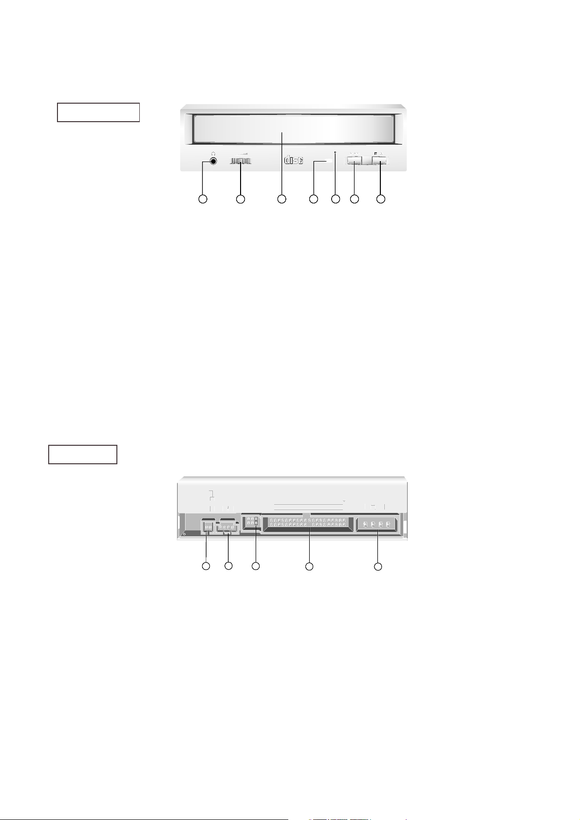
LOCATION OF CUSTOMER CONTROLS
(1) Headphone Jack
3.5mm jack for monitoring the audio signal from audio
CDs.
(2) Headphone Volume Control
Adjusts the headphone sound level.
(3) Disc Drawer
Accepts a CD-ROM disc on its tray.
(4) Busy Indicator
The Busy Indicator lights during initialization and dataread operations.
(5) Emergency Eject Hole
Insert a paper clip here to eject the drawer manually or
when there is no power.
(6) Play/Skip Button
When an Audio CD is in the Disc Drawer, pressing
this button will start playing audio CDs from the first
track. If an audio CD is playing, pressing this button
will skip to the next track.
(7) Open/Close/Stop Button
This button is pressed to open or close the CD tray.
If an audio CD is playing, pressing this button will stop
it, and pressing it
again will open the tray.
COMPACT
1
2
54 6 73
Figure 1. Front View
(1) Digital Audio Output Connector
This is a digital audio output connector or Video CD
output connector.
You can connect this to the digital audio system or
Video CD Board.
(2) Analog Audio Output Connector
The Audio Output Connector connects to a sound
card.
The supplied audio cable is a SoundBlaster
®
type
cable. If you have a different sound card, you will
need to contact the sound card manufacturer to obtain
the proper cable for that card.
(3) Master / Slave / CSEL Jumper
These three jumpers are used to set the CD-ROM
Drive to either a Master, Slave, or CSEL drive.
(4) Interface Connector
This 40-pin connector is used to transfer and control
signals between the CD-ROM Drive and your PC.
Connect the 40-pin IDE cable in your PC to this
connector.
(5) Power-in Connector
Attach a power cable from the computer to this
connector.
Figure 2. Back View
DIGITAL ANALOG
INTERFACE POWER
DR CSM
SLA
GLG39 1
+5
+12
GND
40
2
AUDIO AUDIO
1
2
5
4
3
FRONT
REAR
Figure 2. Back View
Page 4
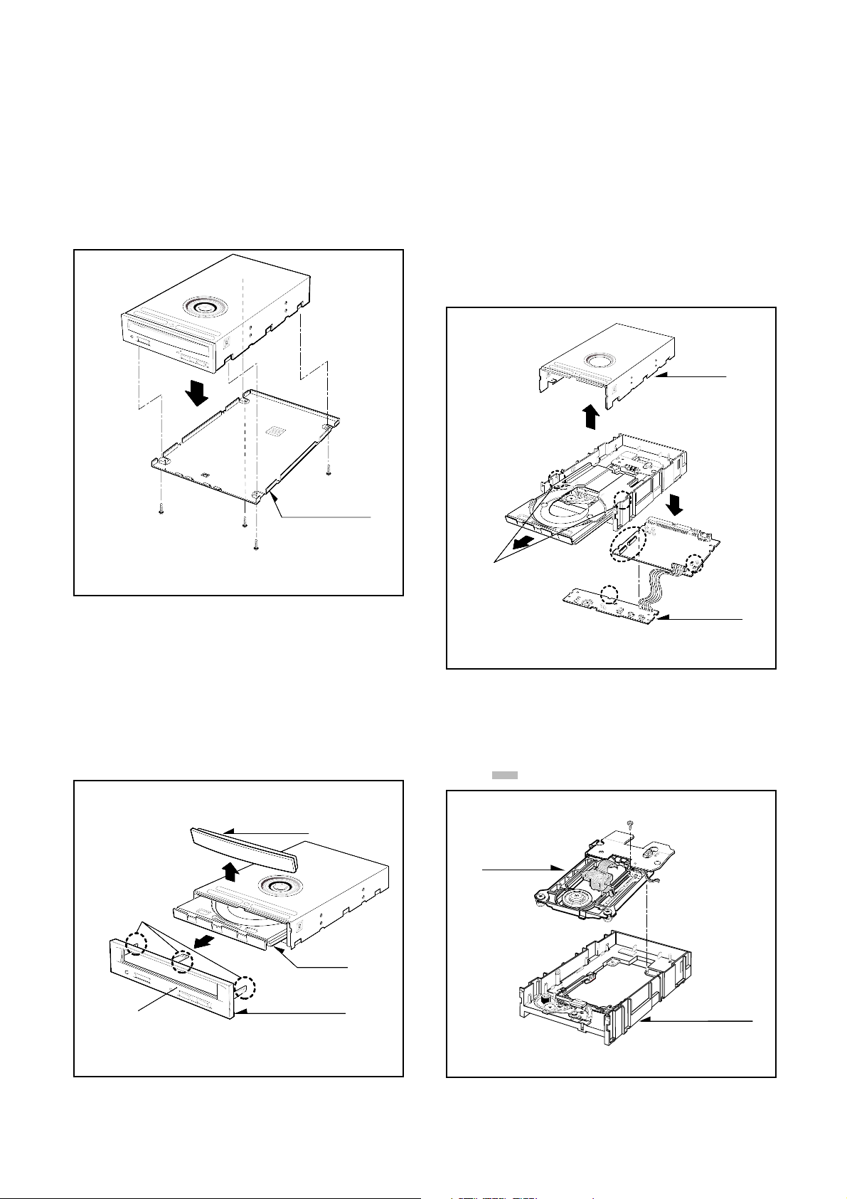
1. CABINET and CIRCUIT BOARD
DISASSEMBLY
1-1. Bottom Chassis
A. Release 4 screws (A) and remove the Bottom
Chassis in the direction of arrow (1). (See Fig. 1-1)
1-2. Front Bezel Assy
A. Insert and Press a rod in the Emergency Eject
Hole and then the CD Tray will open in the
direction of arrow (2).
B. Remove the Tray Door in the direction of arrow (3)
by pushing it outward.
C. Release 3 stoppers and remove the Front Bezel
Assy.
1-3. Cabinet and Main Circuit Board
A. Remove the Cabinet in the direction of arrow (4).
(See Fig. 1-3)
B. Release 2 hooks (a) and remove the CD Tray.
C. Remove the Soldering of the LD- and LD+ (B) for
the Loading Motor, and then remove the Main
Circuit Board.
D. At this time, be careful not to damage the 3
connectors of the Main Circuit Board.
2. MECHANISM ASSY
A. Separate the Pick-Up Unit from the Mechanism
Assy.
B. Release 1 screws (C) and then remove the Pick-
Up ( ).
DISASSEMBLY
(A)
(A)
(A)
(A)
(1)
Bottom Chassis
Fig. 1-1
Fig. 1-2
Fig. 1-3
Fig. 1-4
6
Cabinet
(4)
Hooks (a)
(B)
Main
Circuit Board
Tray Door
(3)
Stoppers
Emergency Eject Hole
(2)
Front Bezel Assy
CD Tray
Pick-up Unit
(C)
Mechanism Assy
Page 5
2. Trouble List (Circuit)
A. LED doesn’t light.
B. Pick-Up doesn’t move to the inner-track.
C. The Laser of Pick-Up doesn’t light.
D. Pick-Up lens doesn’t move up and down.
E. Disc doesn’t rotate.
F. TOC isn’t read. (The LED turns on, but doesn’t flicker.)
G. During Audio CD Play, LED flickers, but Speaker is silent.
21
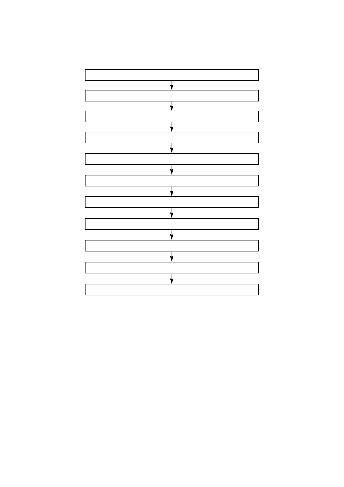
TROUBLESHOOTING GUIDE
1. Initial Lead-in Operation
Reset or Power-On.
LED Flickers.
Pick-Up moves to the inner-Track.
Laser on the Pick-Up lights.
Focus Search (through moving up and down the lens of Pick-Up)
Focus Servo On (FOK Port : H, FEO(TP15) signal generation)
Rotate disc.
Tracking Servo On (TEO(TP14) Signal generation)
Spindle Servo On (MDP(TP25) Signal generation)
Read TOC Area (LED Flickers)
Search the Start of Data Area and then pause.
Page 6
22
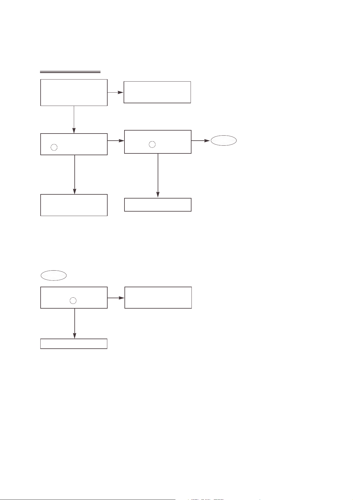
3. Troubleshooting Guide
A. LED doesn’t light.
Check Power Voltage
(TP1:3.3V, TP2:12V, TP20:2.7V)
Reference Voltage
[TP3:DVC(1.35V) and GND.]
Does “H” output in IC501
pin ?
Check and replace R705,
R706, Q701 and LED701
(LED703 for DELL).
Is the CLOCK Frequency of
IC501 pin 33.86MHz?
Check the power input
pattern.
Check IC501.
Check and replace
X501; 33.86MHz,
X502: 40MHz
Is the CLOCK Frequency
of IC501 pin 33.86MHz?
Check and replace IC501.
YES
OK
NG
YES
YES
NO
NO
NO
109
171
171
A-1
A-1
Page 7
23
B. Pick-Up doesn’t move to the inner track.
Do the signals appear at
IC501 pin , ?
(Refer to Fig. B-1.)
Do the signals appear in
PN301 pin?
(Refer to Fig. B-2.)
Does “H” output at IC201
pin ?
Is the 1.35V at IC201 pin ?
Check the pattern from
IC501 pin to IC201
pin
.
Check IC501.
Check the R190 and
then replace IC102.
Check the PN301, and then
replace the Sled Motor.
YES
YES
YES
YES
NO
NO
Replace IC201.
NO
NO
73
41
25
74
106
41
CH1
PIN74
DA0
CH2
PIN73
DA1
CH1 TP4
CH2 TP5
CH3 TP6
CH4 TP7
Fig. B-1. DA0 and DA1 Signals
Fig. B-2. TP4, TP5, TP6 and TP7 Signals
Page 8
Check the pattern from
IC501 pin to R225
and then replace IC501.
24
Does “Low” or “High”
output at IC102 pin ?
Is the voltage of IC102 pin
(LD) 2V?
Check Pick-Up FFC, PN101.
Check Q101, C101, C102
and then replace IC102.
Check R118 and replace IC501.
YES
YES
NO
NO
1
4
12
Does the focus search signal
appear at FAO (TP9)?
(Refer to Fig. D-1.)
Is the 1.35V at IC201 pin ?
Check the R190 and then
replace IC102.
YES
YES
YES
NO
NO
Replace IC201.
NO
25
Does the focus search
signal appear between F+
(TP10) and F- (TP11)?
(Refer to Fig. D-2.)
C. The Laser of Pick-Up doesn’t light.
D. The Pick-UP lens doesn’t move up and down.
D-1
Page 9

25
Check the pattern from
pin , of IC201 to
pin , of PN101.
Check the PN101, Pick-Up
FFC.
Replace the Pick-Up.
Replace PN101 or Pick-Up
FFC.
OK
OK
NG
34
35
1
4
CH1
TP9
(FAO)
CH1
TP10(F+)
TP11(F-)
Fig. D-1. FAO Signal
Fig. D-2. Focus Search Signal
D-1
Page 10

26
Does the signal appear at
the MDP (TP25)?
(Refer to Fig. E-4.)
Do the signals appear at
IC201 pin (W), (V),
and (U)?
Replace IC501.
Replace IC201.
YES
NO
NO
12
14
13
Check the pattern from
IC201 pin , , to
PN201 , , .
YES
OK
12
13
14
13
12
11
Check Spindle Motor FFC
and then replace the
Spindle Motor.
Does the signal appear at
FEO (TP15) when the
R504 opened?
(Refer to Fig. E-2.)
YES
YES
YES
NO
NO
Replace IC501.
Replace IC501.
Replace Pick-Up.
NO
Do the signal appear at
TP15 (FEO)?
(Refer to Fig. E-3.)
Does the signal appear at
FOK (TP18) during focus
search?
(Refer to Fig. E-1.)
E. Disc doesn’t rotate.
Page 11

27
Fig. E-3. FEO Signal
CH1
TP15:
FEO
Fig. E-4. MDP Signal
CH1
TP25:
MDP
Fig. E-1. FOK, F+ Signal
CH1
TP10:
F+
CH2
TP18:
FOK
Fig. E-2. S-Curve (R505:Open)
CH1
TP15:
S-Curve
Page 12

28
Is the Focus Servo ON?
(Does FEO (TP15) signal
appear?)
Does A, B, C, D signal
appear at IC102 pin ,
, , ?
YES
YES
NO
6
7 8 9
NO
Is the Tracking Servo ON?
(Does TEO (TP14) signal
appear?)
Does E, F signal appear
at IC102 pin , ?
YES
NO
10
YES
Is TOC area on the disc
read? (Does LED flicker?)
Does the other disc
operate normally?
Normal Disc is defective.
YES YES
NO
11
NO
Does RFAC signal (TP16)
and RFDC signal (TP17)
appear?
Is Spindle Servo ON?
(Does MDP signal (TP25)
appear?)
YES YES
NO
NO
NO
Does A, B, C, D signal
appear at IC102 pin ,
, , ?
6
7 8 9
Replace IC102.
Replace IC102.
Replace IC501.
Replace Main Circuit
Board or MD Ass’y.
NO
Refer to C.
(The Laser of Pick-Up
doesn’t light.)
F. TOC isn’t read.
Page 13

29
Does PWM signal appear at
IC501 pin , , , ?
(Refer to Fig. G-1.)
YES
NO
166 167
174
175
Replace IC501.
Replace IC601.
Does Audio signal appear
at IC601 pin , ?
(Refer to Fig. G-2.)
YES
YES
NO
3
12
Is the voltage of IC601
pin and 2.5V?
9
NO
Check the C602.
8
Does “H” signal appear at
IC501 pin ?
YES
NO
108
Check the IC501 pin
and then replace IC401.
108
Check C702.
YES
YES
YES
Are L-ch, R-ch signals
appear at JK701 and
Audio Line out connector
each?
NO
Check JK701 and
L701,L703.
Does Audio signal appear
at IC701 pin , ?
NO
1 7
Is the voltage of IC701
pin 2.5V?
6
NO
Replace IC701.
G. During Audio CD play, LED flickers, but Speaker is silent.
G-1
Page 14

30
Is the connection
between JK801 (or Audio
Line out connector) and
Line (or Jack) normal?
NO
Check the JK801 and
Audio line pattern.
YES
Check your sound card,
Audio Cable, Speaker,
Volume and Headphone
Jack.
Fig. G-1. PWM Signal
CH1
PIN6 of
IC601
CH2
PIN10 of
IC601
Fig. G-2. Audio Signal
CH2
PIN3 of
IC601
CH2
PIN12 of
IC601
G-1
Page 15

12
PHOTO DIODE STRUCTURE OF THE PICK-UP
(1) Focus Error Signal –> (A+C)-(B+D)
(Control the Pick-up’s up and down to focus on the Disc)
(2) Tracking Error Signal –> (E-F)
(Control the Pick-up’s left and right shift to find the track on the Disc)
(3) RF Signal –> (A+B+C+D)
(
RF Signal is converted to Data Signal in One Chip IC (IC501))
Three signals (Focus Error Signal, Tracking Error Signal and RF Signal) above are I-V converted and
amplified at the IC102, and then are transmitted to One Chip IC (IC501) to generate the Servo Control
Signal and Data Signal.
Red laser
Pick-Up module
Tracking
Focusing
B
C
E
F
D
A
Page 16

13
AC
SUM
AC
VCA
EQ
EQ_ON/OFF
RW/ROM
RW/ROM
RW/ROM
RW/ROM
RW/ROM
RW/ROM
RW/ROM
VC
VC
VC
DVC
DVC
DVcc
DVcc
DVcc
DVcc
DVcc
VOFST
AABBCCD
D
6
4 3 23 24 26
25
7
8
9
E
10
F
11
12
22 5
27
14
gm
gm
VOFST
VOFST
DVC
DVC
DVC
DVC
AVC
AVC
AVC
Vcc
Vcc
APC-OFF (Hi-Z)
(H/L)
APC
SW
PD
LD
Vcc
GND
AVC
DVC
2
1
13
CE20CEI
TE
21
18
TE_BAL19FE16FEI
RFDCO
RFDCI
DC_OFST
17
28
29
30
RFAC
15
AC_SUM
EQ_IN
RFG
BST
RFC
VFC
Pin No.
Symbol I/O Description
Pin No.
Symbol I/O Description
1 LD O APC Amp Output 16 FE O Focus Error Amp Non-inverted Output
2 PD I APC Amp Input 17 FEI – Focus Error Amp Inverted
3EQ–IN I
RFAC VCA Block, EQ Block Input
18 TE O Tracking Error Signal Output
4AC–SUM O
RFAC RF SUM Output
19 TE_BAL I TE Control
5 GND I GND 20 CE O Center Error Signal Output
6 A I RF Input (A Signal) 21 CEI – CE Amp Inverted
7 B I RF Input (B Signal) 22 Vcc I Vcc
8 C I RF Input (C Signal) 23 RFG I RFAC Low Frequency Gain Control
9 D I RF Input (D Signal) 24 BST I EQ Boost Volume Control
10 E I RF Input (E Signal) 25 VFC I EQ Cut OFF Frequency Control
11 F I RF Input (F Signal) 26 RFC I EQ Cut OFF Frequency Control
12 SW I
Mode Switching Signal Input
27 VC O VC Output
13 DVcc I DVcc 28 RFDCO O RFDC Output
14 DVC O DVC Output 29 RFDCI – RFDC Amp Inverted
15 RFAC O RFAC Summing Equalized Output 30
DC_OFST
– RFDC Signal Output Control
Pin Description
IC INTERNAL BLOCK DIAGRAM AND PIN DESCRIPTION
• IC102 (CXA2581N) : RF Amplifier IC
I-V converts and amplifies the signal received from the pick-up and then applies to DSP part of onechip IC (IC501).
Block Diagram
Page 17

14
• IC201 (M63021FP) : Drive IC (Spindle/Servo Actuator)
Rotates the Spindle Motor by receiving MDP signal from IC501.
Generates the signal to drive Focus Actuator Coil, Tracking Actuator Coil, Sled Motor, and Stepping
Motor by Control Signal input from DSP and u-COM.
Block Diagram
x12
x8
x12
FG
HU+
HUHV+
HV-
HW+
HWHB
SPIN
REF
SL1IN
SL2IN
FOIN
TOIN
5Vcc
TO+
TO-
FO+
FO-
GND
LO+
LO-
VM3
LOIN+
BRS
OSC
MU1
S
SS
S
VM1
RSPUV
W
RSL1
RSL2
SL1+
SL1-
SL2+
SL2-
VM2
FG
Reverse
Detect
120ß
MATRIX
Hall Bias
CTL
amp
Direction
comp
Direction
comp
Direction
comp
Current
comp
Current
comp
Current
comp
CTL
amp
CTL
amp
Logic
Logic
TSD
BIAS
Frequency
generator
VM1
Regulator
Reg
Pin Description
Pin No.
Symbol Description
Pin No.
Symbol Description
1 SL1IN Slide control voltage input 1
2 SL2IN Slide control voltage input 2
3 VM2 Motor Power Supply 3 (for Slide)
4 RSL2 Slide current sense 2
5 SL2+ Slide non-inverted output 2
6 SL2- Slide inverted output 2
7 GND GND
8 RSL1 Slide current sense 1
9 SL1+ Slide non-inverted output 1
10 SL1- Slide inverted output 1
11 GND GND
12 W Motor drive output W
13 V Motor drive output V
14 U Motor drive output U
15 RSP Spindle current sensie
16 HW- HW- sensor amp. input
17 HW+ HW+ sensor amp. input
18 HV- HV- sensor amp. input
19 HV+ HV+ sensor amp. input
20 HU- HU- sensor amp. input
21 HU+ HU+ sensor amp. input
22 VM1 Motor Power Supply 1 (for Spindle)
23 HB Bias for Hall Sensor
24 FG Frequency generator output
25 REF Refernce voltage input
26 SPIN Spindle control voltage input
27 FOIN Focus control voltage input
28 TOIN Tracking control voltage input
29 GND GND
30 5VCC 5V Power Supply (for FS, TS)
31 TO- Tracking inverted output
32 TO+ Tracking non-inverted output
33 GND GND
34 FO+ Focus non-inverted output
35 FO- Focus inverted output
36 LO+ Loading non-inverted output
37 LO- Loading inverted output
38 BRS Brake select control terminal
39 VM3 Motor power supply 3.(for Loading)
40 LOIN+ Loading control input( +)
41 MU1 Mute 1
42 OSC PWM carrier oscilation set
Page 18

1Mbits DRAM
CLOCK
GEN
DATA
processor
DMA SEQUENCER
ADDRESS GEN
(Serial I/F)
CLOCK
GEN
PRIORITY RESOLVER
Subcode
Deinterleave & ECC
MAIN DATA
ERROR CORRECTION
ATAPI REGISTERS
12byte PACKET FIFO
HOST
I/F
DESCRAMBLER
SYNC CONTROL
Sub CPU I/F
DRVss
DRV
DD
HDB0~F
139~142,
145~148,
151~154,
156~159
HCS0,1
123~125
121,122
HA0~2
XHRD
XHWR
XHAC
HDRQ
HINT
XS16
REDY
D0~7*
A0~6*
DASP
XPDI
HAST
137
119
120
130
127
128
136
129
135
134
DMA FIFO
Digital OUT
8fs
1bit DAC
Error
Correction
block
Subcode P~W
Processor
32K RAM
EFM
Timing Generator
Subcode Q
Processor
XRD*
XWR*
XCS*
XTL1
XINT*
XWAT*
XTL2
PWM2N
PWM2P
FOK
PWM1N
175 167 166 161 162
PWM1P
MIRR
DFCT
174
OP Amp
DACSERVO DSP
Auto Sequencer
8bit
A/D
OP Amp
Analog SW
SAO
TAO
FAO
BSSD
DOUT
DAC
I/F
CD-DSP
I/F
CPU Interface
FOK
MIRR
DFCT
XTLO XTLI
170 171
Digital PLL
ASY
Sync protector
PCO
VDD
Vss
52
FILI
51
FILO
50
CLTV
53
ASYI
57
ASYO
58
WFCK
SCOR*
29
RFDC
CE
TESEFE
VC
SQCK*
SQSO*
SENS*
COUT*
MDP
PWMI
ADIO
RFAC
55
CLV/CAV
Processor
SERVO BLOCK
DAC BLOCK
DATA BLOCK
19
20
41424344454647
5 4 3 2 21 65 64 16
15
• IC501 (CXD3035R) : DSP+ATAPI DECODER+DRAM+µ-COM
Block Diagram
*
is connected to µ-com port inside.
Page 19

16
• IC501 CXD3035R
Pin Description
Pin No. Symbol I/O Description
1 AVS6 Analog GND
2 SAO O Analog DAC Analog Output of Slide Filter
3 TAO O Analog DAC Analog Output of Tracking Filter
4 FAO O Analog DAC Analog Output of Focus Filter
5 BSSD I Constant Current Input for DAC Analog of Servo Filter
6 AVD6 Analog Power Supply (2.5V)
7 VSIO0 Digital GND
` 8 SFDF O 1,0 Control Output of stepping Motor
9 SFDR O 1,0 Control Output of stepping Motor/SLED drive
10 SRDF O 1,0 Control Output of stepping Motor
11 SRDR O 1,0 Control Output of stepping Motor/SLED drive
12 VDC0 Digital Power Supply (2.5V)
13 RMUT O 1,0 Audio DAC, Rch Zero Detection Play/PWM0*/COUT*/Signal Output
14 LMUT O 1,0 Audio DAC, Lch Zero Detection Play/RWM1* Signal Output
15 VSC0 Digital GND
16 DOUT O 1,0 Digital-Out Output
17 VDIO0 Digital Power Supply (3.3V)
18 SSTP I Disc Inner Track Detection Signal Input
19 MDP O 1,Z,0 Control Output of Spindle Motor
20 PWMI I External Terminal Input of Spindle Motor
21 DFCT I/O 1,0 Defect Signal In/Output
22 ATSK I Pin for Anti-Shock. It set to “L” When is not used.
23 MNT0 O 1,0 MNT0/XRAOF* Signal Output
24 MNT1 O 1,0 MNT1/C2PO* Signal Output
25 MNT2 O 1,0 MNT2/XUGF* Signal Output
26 MNT3 O 1,0 MNT3/GTOP* Signal Output
27 XPLCK O 1,0 XPLCK/WDCK*/C2PO*/PWM4* Signal Output
28 VSIO1 Digital GND
29 WFCK O 1,0 WFCK/LRCK*/BLRCK*/PWM2* Signal Output
30 RFCK O 1,0 RFCK/PCMD*/BPCMD*/PWM3* Signal Output
31 LOCK O 1,0 LOCK/BCK*/BBCK* Signal Output
32 VDC1 Digital Power Supply (2.5V)
33 MTST3 I Test Pin. Normally “L”
34 VSC1 Digital GND
35 MTST2 I Test Pin. Normally “L”
36 MTST1 I Test Pin. Normally “L”
37 VDIO1 Digital Power Supply (3.3V)
Page 20

17
Pin No. Symbol I/O Description
38 AVD2 Analog Power Supply (2.5V)
39 IGEN I Resistor Connection Pin of Current Source Reference for OP Amp
40 AVS2 Analog GND
41 ADIO O Analog OP Amp Output
42 RFDC I RF Signal Input
43 CE I Center Servo Analog Input
44 TE I Tracking Error Signal Input
45 SE I Slide Error Signal Input
46 FE I Focus Error Signal Input
47 VC I Center voltage Input
48 VPCO1 O 1,Z,0 Output of VCO2 for Wide-Band EFM PLL
49 VCTL I Input of VCO2 Control voltage for Wide-Band EFM PLL
50 FILO O Analog Filter Output for Master PLL (Slave = Digital PLL)
51 FILI I Filter Input for Master PLL
52 PCO O 1,Z,0 Change Pump Output for Master PLL
53 CLTV I Multiplier VCO Control Voltage Input
54 AVS1 Analog GND
55 RFAC I EFM Signal Input
56 BIAS I Asymmetry Circuit Constant Current Input
57 ASYI I Asymmetry Comparator Voltage Input
58 ASYO O 1,0 EFM Full-Swing Output (L=V
SS, H=VDD)
59 AVD1 Analog Power Supply (2.5V)
60 VDC2 Digital Power Supply (2.5V)
61 VDC3 Digital Power Supply (2.5V)
62 VSC2 Digital GND
63 VSC3 Digital GND
64 FOK I/O 1,0 Focus OK Signal IN/OUT
65 MIRR I/O 1,0 Mirror Signal IN/OUT
66 GFS O 1,0 GFS Output
67 PG7/SCKZ0 Serial Clock In/Output port
68 PG6/SO0
I/O 1,0
Serial Data Output
69 PG5/SI0 Serial Data Input
70 PG4/SCSZ0 Serial chip select Input
71 PG3/XWP (Port G) In/Output port as 1 bit Write protect output port
72 PG2/XONBR
I/O 1,0
Active Hard Reset Input port
73 PG1/PWM1/DA1
74 PG0/PWM0/DA0
75 DRV
DD
0 Internal DRAM Exclusive Power Supply
(Port G)
IN/Output port as 1 bit
(Port G)
IN/Output port as 1 bit
14 bit PWM Output port
DA Gate pulse Output port
Page 21

18
Pin No. Symbol I/O Description
76 DRV
SS
0 Internal DRAM Exclusive GND
77 VSIO2 Digital GND
78 VDIO2 Digital Power Supply (3.3V)
79 PF7/T2 16 bit capture timer/counter Output port
80 PF6/T1
I/O 1,0
8 bit timer/counter Output port
81 DRV
DD
1 Internal DRAM Exclusive Power Supply
82 DRV
SS
1 Internal DRAM Exclusive GND
83 PF5
84 PF4
85 PF3 I/O 1,0
86 PF2/NM1Z Non maskable interrupt input port
87 PF1/EC2Z
16 bit capture timer/counter external Event input port
88 PF0
89 PE7/CINT 16 bit capture timer/counter capture Input port
90 PE6
91 PE5
92 PE4/INT4Z I/O 1,0 External interrupt Input port
93 PE3/INT3Z
94 PE2
95 PE1
96 PE0
97 VSIO3 Digital Power Supply GND
98 PC7
99 PC6
100 PC5
101 PC4 I/O 1,0 (Port C)
102 PC3 8 bit In/Output port
103 PC2
104 PC1
105 PC0
106 PB7
107 PB6
108 PB5
109 PB4 I/O 1,0 (Port B)
110 PB3 8 bit In/Output port
111 PB2
112 PB1
113 PB0
(Port F)
IN/Output port as 1 bit
(Port F)
IN/Output port as 1 bit
(Port E)
IN/Output port as 1 bit
Page 22

19
Pin No. Symbol I/O Description
114 VDIO3 Digital Power Supply (3.3V)
115 OEXTAL O 1,0 Crystal Oscillating Circuit Output for the Master Clock
116 EXTAL I Crystal Oscillating Circuit Intput for the Master Clock
117 VDIO4 Digital Power Supply GND
118 RSTZ I System Reset,“L” is reset
119 XPDI I/O Z,0 Passed Diagnostics Signal, Open Drain Output, Negative Logic
120 DASP I/O Z,0 Drive Active/Slave Present Signal, Open Drain Output, Negative Logic
121 HCS1 I Chip Select Negative Signal from Host
122 HCS0 I Chip Select Negative Signal from Host
123 HA2 I Host Address (MSB)
124 HA0 I Host Address (LSB)
125 HA1 I Host Address
126 VDC6 Digital Power Supply (2.5V)
127 XS16 O Z,0 Host 16-bit I/O Port Select Signal, Open Drain Output, Negative Logic
128 HINT I/O 1,Z,0 Host Interrupt Demand Signal, Positive Logic
129 XHAC I DMA Acknowledge Signal from Host, Negative Logic
130 REDY O Z, 0 Host I/O Channel Ready Signal, Open Drain Output, Negative Logic
131 VDIO4 Digital Power Supply (3.3V)
132 VDC4 Digital Power Supply (2.5V)
133 VSC4 Digital GND
134 XHRD I Data Read Strobe Signal from Host
135 XHWR I Data Write Strobe Signal from Host
136 HDRQ O 1, Z, 0 DMA Request Signal to Host, Positive Logic
137 XHRS I Chip Reset Signal from Host, Negative Logic
138 VDIO5 Digital Power Supply (3.3V)
139 HDBF I/O 1,Z,0 Host Data Bus (MSB)
140 HDB0 I/O 1,Z,0 Host Data Bus (LSB)
141 HDBE I/O 1,Z,0 Host Data Bus
142 HDB1 I/O 1,Z,0 Host Data Bus
143 VSIO5 Digital Power Supply GND
144 VSIO6 Digital Power Supply GND
145 HDBD I/O 1,Z,0 Host Data Bus
146 HDB2 I/O 1,Z,0 Host Data Bus
147 HDBC I/O 1,Z,0 Host Data Bus
148 HDB3 I/O 1,Z,0 Host Data Bus
149 VDIO6 Digital Power Supply (3.3V)
150 VDIO7 Digital Power Supply (3.3V)
151 HDBB I/O 1,Z,0 Host Data Bus
152 HDB4 I/O 1,Z,0 Host Data Bus
Page 23

20
Notes :
• LRCK, BCK and PCMD are changed to 32-bit slot and 48-bit slot by command.
32-bit slot is output in 2's complements on an LSB-first basis and 48-bit slot is output in 2's complements on
an MSB-first basis.
• *'s signal is able to convert to output by a command.
• The GFS signal turns "H" upon coincidence between Frame Sync and the timing of interpolation protection.
• XRAOF is a signal issued when a jitter margin of +28F is exceeded by the 32K RAM.
• C2PO is a signal to indicate data error.
• XUGF is a negative Frame Sync pulse obtained from the EFM signal before Frame Sync protection is
effected.
• GTOP monitors the state of Frame Sync protection. ("H" : Sync protection window released)
• XPLCK is an inversion of the EFM PLL clock. The PLL is designed so that the falling edge of XPLCK
coincides with a change point of the EFM signal.
• RFCK is a signal generated at 136-µs periods using a crystal oscillator.
• LOCK is sampling the GFS at 460Hz and outputs "H" when GFS is "H".
("L" outputs when "L" is output eight times in succession or inputs when LKIN is "H".)
Pin No. Symbol I/O Description
153 HDBA I/O 1,Z,0 Host Data Bus
154 HDB5 I/O 1,Z,0 Host Data Bus
155 VSIO7 Digital Power Supply GND
156 HDB9 I/O 1,Z,0 Host Data Bus
157 HDB6 I/O 1,Z,0 Host Data Bus
158 HDB8 I/O 1,Z,0 Host Data Bus
159 HDB7 I/O 1,Z,0 Host Data Bus
160 VDC5 Digital Power Supply (2.5V)
161 XTL2 O 1, 0 Crystal Oscillating Circuit Output of the Clock for Decoder
162 XTL1 I Crystal Oscillating Circuit Input of the Clock for Decoder
163 VSC5 Digital GND
164 MTST0 I Test Pin. Normally “L”
165 AVS3 Analog GND
166 PWM2N O 1, 0 PWM Output of Audio DAC. Default R Ch, Reverse Phase
167 PWM2P O 1, 0 PWM Output of Audio DAC. Default R Ch, Forward Phase
168 AVD3 Analog Power Supply (2.5V)
169 AVD4 DSP, Power Supply for Audio DAC Clock (2.5V)
170 XTLO O 1,0 DSP, Crystal Oscillating Circuit Output for the Audio DAC Clock
171 XTLI I DSP, Crystal Oscillating Circuit Input for the Audio DAC Clock
172 AVS4 DSP, GND for the Audio DAC Clock
173 AVS5 Analog GND
174 PWM1P O 1, 0 PWM Output of Audio DAC. L Ch, Forward Phase
175 PWM1N O 1, 0 PWM Output of Audio DAC. L Ch, Reverse Phase
176 AVD5 Analog Power Supply (2.5V)
Page 24

3.3V Reg
2.7V Reg
+3.3V
+5V
+12V
+2.7V
GND
GND
+5V
+12V
GND
GND
SPINDLE
MOTOR
SLED
MOTOR
LOADING
MOTOR
FOCUS
COIL
TRACKING
COIL
M63021FP
MOTOR DRIVE
Disc
Motor unit
Optical
Pick-up
CXA2581N
RF Amp.
CXD3035R
DSP + Decoder +
DRAM +
System controller
33.86MHz
40MHz
I/F Cable
H
O
S
T
AUDIO
Circuitry
R-ch
L-ch
Line-out
A B CD
1
2
3
4
5
32
BLOCK DIAGRAM
* MODEL: CRD-8481B/CRD-8401B
Page 25

PBM00 (MAIN C.B.A)
007
002
003
030
020
A02
A01
020
051
032
050
029
434
021
434
434
413
413
413
001
413
430
028
027
026
025
033
435
013
010
009
008
011
012
005
034
014
420
434
031
016
015
004
006
431431
A B C D E F GH
1
2
3
4
5
EXPLODED VIEW
7
8
 Loading...