

Page 1

3
GENERAL FEATURE
SPECIFICATIONS
1. SUPPORTED SYSTEM
• IBM Compatible 486SX or Above
2. SUPPORTED OS
3. GENERAL PERFORMANCE
• Data Transfer Rate..........................................................................................Sustained Data Transfer Rate
.............................................................................................10 Times Speed (Inner side) : 1,500 kbytes/sec
.............................................................................................24 Times Speed (Outer side): 3,600 kbytes/sec
• Data Buffer Capacity..........................................................................................1 Mbit DRAM (Internal DSP)
• Access Time ............................................................................................Random Access : Average 110 ms
4. POWER REQUIREMENTS
• Voltage........................................................................................................................................+5V DC+5%
• Ripple....................................................................................................................................+5V : 100mVp-p
• Current .........................................................................................Peak in executing access : 1,000mA MAX
................................................................................................................................Random access : 800mA
..............................................................................................................................Normal operation : 700mA
..............................................................................................................................................Standby : 30mA
..................................................................................................................................................Sleep : 30mA
5. AUDIO PERFORMANCE
• Frequency Response......................................................................................................20Hz~20KHz( dB)
• S/N Ratio (IHF-A)..................................................................................................70 dB (Typical, 1KHz 0dB)
• Distortion (20K-LPF) ............................................................................................0.05% (Typical, 1KHz 0dB)
• Channel Separation ................................................................................................................65 dB (Typical)
• Dynamic Range (IHF-A)..........................................................................................................70 dB (Typical)
• Output Level (47kΩ Load).................................................................................................0.75Vrms (Typical)
• Enhanced IDE interface
• Ultra Slim type CD-ROM drive
(Height: 12.7mm)
• Fast 110ms Average Access Time
• MAX 3,600KB/sec (24X) Sustained Transfer
rate
• Photo-CD Multisession Disc Spec compliant
• MPC level 3 Spec compliant
• Drawer Type Manual load/Electrical Release
• 3-Way eject support (Software, Open button,
Emergency eject)
• Built-in ATAPI Interface Controller
• Closed enclosure
• Software Volume Control
• 8 Times Digital Filter for CD Audio
• Built-in MODE-1 ECC/EDC
• MTBF 60,000h POH (at 10% Utilization)
• PIO Mode 4 & Multi-word DMA Mode 2
support & Ultra DMA Mode2 support
• Digital audio through ATAPI Interface
• Spin-down Mode for energy saving
• Support Standby & Sleep mode
• MS-DOS Version 3.1 or Windows 3.1
• OS/2 Warp (Ver 3.0 & 4.0) or higher
• Windows '95 or ‘98 higher
• Windows 2000
• Windows NT (Version 3.51 or 4.0) or higher
+1
-3
Page 2

4
1. CABINET
A. Release 3 screws (A).
B. Lift up the Cabinet in the direction of arrow (1).
(See Fig. 1)
2. MAIN CIRCUIT BOARD
A. Insert and press a rod in the Emergency Eject
Hole and then the CD Tray will open in the
direction of arrow (2).
B. Release 2 screws (B).
C. Remove the Main Circuit Board.
3. FRONT PANEL
A. Release 5 screws (C) and remove the Cover
Bottom.
B. Remove the Front Panel.
C. At this time, be careful not to damage the 5 hooks
(a) of the it.
4. BASE PICK-UP
A. Remove the Base Pick-Up.
(1)
(A)
(A)
(A)
Fig. 3
Fig. 1
Fig. 4
(B)
(B)
(2)
Fig. 2
DISASSEMBLY
CABINET
HOOKS
MAIN CIRCUIT BOARD
FRONT PANEL
ASSY
HOOK (a)
COVER
BOTTOM
BASE PICK-UP
EMERGENCY
EJECT HOLE
(C)
(C)
Page 3

10
REF
REFREF
REF
REF
REF
REF
REF
REF
REF
REF
REF
REF
REF
REF
VCC
VCC
VCC
APC
PH
PH
EQ-CONTROL
BH
BH
PH-CONTROL
7_MODE
5V
39K
33K
52
5V
+
7_MODE
36
PH
100K
1
2
3
4
5
6
7
BHC
PHC
RFAO
GND1
RFA-
RFIN
FIN1
35
BH
34
VCC1
33
RFSM
32
RHLD
31
GND2
30
REFL
29
FE-
28
FE
27
TE-
26
TE
25
TSS
24
TS
23
VCC2
22
TSH
21
FBAL
20
TBAL
19
SGC
100K
8
FIN2
56K
9
E
F
VCC
56K
10
11
12
REFI
VREF
13
LDD
14
LDS
15
LDON
16
GHS
17
BHH
18
EQS
IC INTERNAL BLOCK DIAGRAM AND PIN DESCRIPTION
IC101 (LA9239) : RF Amplifier IC
I-V converts and amplifies the signal received from the pick-up and then applies to DSP part of onechip IC (IC501).
Block Diagram
Page 4

Pin No. Pin Name Descriptions
1 BHC Bottom hold external condensor pin for checking RFAGC.
2 PHC Peak hold external condensor pin for checking RFAGC.
3 RFAO RF Pre AMP output
4 GND RF GND
5 RFA- RF Pre AMP (-) input
6 RFIN RF Sum input
7 FIN1 Pickup output (B+D),
8 Fin2 Pickup output (A+C),
9 E Pickup output (E)
10 F Pickup output (F)
11 REFI Eeternal Condensor Pin of Reference Voltage.
12 VREF Reference output
13 LDD APC circuit output
14 LDS APC circuit input
15 LDON Laser on/off.
16 GHS RF signal gain control.
17 BHH BH response control.
18 EQS RF equalizer. PH detection control
19 SGC Servo gain control
20 TBAL TE balance adjust
21 FBAL FE balance adjust
22 TSH TS wide band control
23 VCC2 Servo VCC
24 TS TS output
25 TSS TS wide band control
26 TE TE signal output (To DSP)
27 TE- TE gain control
28 FE FE signal output (To DSP)
29 FE- FE gain control
30 REFL Reflection output (To DSP)
31 GND2 Servo GND
32 RHLD RF hold control
33 RFSM EFM signal output (To DSP)
34 VCC1 RF VCC
35 BH RF bottom hold output (To DSP)
36 PH RF peak hold output (To DSP)
Pin Description
11
Page 5
12
H1H
VDD
15kΩ
IN1
FB1
IN2
FB2
IN3
FB3
CT
VREF
STBY
0.012µF
1kΩ
1.1kΩ
H1L
16
44
25
14
H2H
H2L
13
12
H3H
H3L
VH
FG
FG Signal Output
Spindle Speed
Control Input
SFG
SBR
EC
ECR
VP
V
CL
SRESET
SSET
V
T
VN VO
GND
CS
RCS6
RCS5
RCS4
RCS3
RCS2
RCS1
A3
A22
A21
A1
VMSP2
VMSP1
BC2
BC1
11
10
9
7
6
50
18
17
19 20 21
40
51
3
4
53
54
55
1
52
8
49
37
38
VPUMP
39
PGSL
27
RO3
26
FO3
28
VMSL
22
PGAC
31
RO2
29
FO2
30
RO1
FO1
VMAC
32
35
36
15kΩ
20kΩ
20kΩ
20kΩ
0.012µF
0.012µF
100pF
1.65V
22µF
5V
47µF
100Ω
Rcs=
0.33Ω
5V
100µF
5V
47µF
0.1µF
0.1µF
100Ω
1kΩ
15kΩ
FF
Divide
Circuit
Hall
Comp
Matrix
5
56
2
H:active
L:standby
H:3FG
L:1FG
H:S-BRK
L:R-BRK
45
34
24
41
43
47
46
23
Absolute
value
S-BRK
Conversion
FG
Generator
Hall
Bias
+
X5
Upper
Drive
Low
Drive
DMOS
3-Phase
Bridge
OSC
Charge
Pump
DMOS
H/B
DMOS
H/B
DMOS
H/B
Drive
Logic
A
B
S
A
B
S
A
B
S
FB
FB
FB
Logic
Logic
Delta wave
Oscillator
VREF Reset
Stand-by
VDD Reset
Heat
Protection
Drive
Drive
M
IC201 (AN8498SH) : Servo Actuator Drive IC
Generates the signal to drive Focus Actuator Coil, Tracking Actuator Coil, Sled Motor, and Stepping
Motor by Control Signal input from DSP and u-COM.
Block Diagram
Page 6

13
Pin No
Symbol Description
1 A22 SP Drive Output 2
2 RCS6 SP Power Source 6
3 RCS5 SP Power Source 5
4 RCS4 SP Power Source 4
5 A3 SP Drive output 3
6 SFG SP FG mode conversion
7 FG SP FG signal output
8 VMSP2 SP Motor power supply 2
9 VH SP Hall Bias
10 H3L SP Hall (-) input 3
11 H3H SP Hall (+) input 3
12 H2L SP Hall (-) input 2
13 H2H SP Hall (+) input 2
14 H1L SP Hall (-) input 1
15 N.C. N.C.
16 H1H SP Hall + input 1
17 ECR SP Torque Reference input
18 EC SP Torque input
19 VP Op amp Non-inverted input
20 VN Op amp inverted input
21 VO Op amp output
22 VMSL Ch3 power supply
23 IN3 Ch3 input
24 FB3 Ch3 feedback output
25 STBY Stand-by
26 RO3 Ch3 inverted output
27 PGSL Ch3 Power GND
28 FO3 Ch3 Non-inverted output
Pin Description
Pin No
Symbol Description
29 RO2 CH2 inverted Output
30 FO2 CH2 Non-inverted Output
31 PGAC CH1, 2 Power GND
32 RO1 CH1 Inverted Output
33 N.C. N.C.
34 CT 3 Delta-wave Output
35 FO1 Ch1 Non-inverted Output
36 VMAC Ch1, 2 Power Supply
37 BC2 Charge Pump Volume Connector2
38 BC1 Charge Pump Volume Connector1
39 VPUMP
Charge Pump Boost the Voltage of Output
40 GND GND
41 IN1 CH1 Input
42 N.C. N.C.
43 FBI CH1 Feedback Output
44 VDD Control Circuit Power Supply
45 VREF Reference Voltage Input
46 FB2 CH2 Feedback Output
47 IN2 CH2 Input
48 N.C. N.C.
49 VMSP1 SP Motor Power Supply
50 SBR SP Break mode conversion
51 CS SP Voltage Defected Output
52 A1 SP Drive Output1
53 RCS3 SP Power Source 3
54 RCS2 SP Power Source 2
55 RCS1 SP Power Source 1
56 A21 SP Drive Output 2
Page 7

14
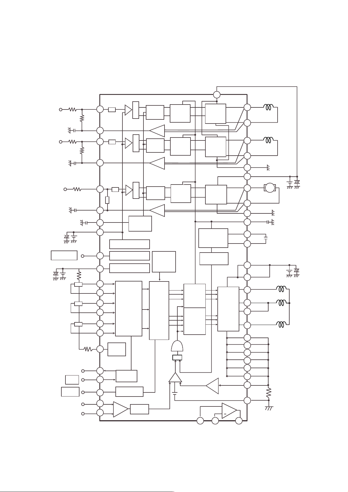
IC501 (HMS985300) : DSP+ATAPI DECODER+ASP+System Controller
Driver
VCEC
PLL
TDO, FDO
SLDO, SPDO
*11
*1
*12
*2
*14
*3
*4
*5
*6
LA9238
CD-DSP
Data bus[0.7]
DRAM
Data bus[0.15]
LC895300
LC895299
Adress bus[0.18]
Sub-code I/F
de-interleve
Adress generator
Sub-code ECC
Address generator
Address generator
Address generator
Address generator
Address generator
ATAPI I/F
Data output input I/F
Microcontroller
RAM access
De-scramble &
Buffering
ECC & EDC
SRAM
CD-DSP I/F
& SYNC
Detector
Merge
EXT10
CMDI
Each Block
Register
FGCNT
Audio
Circuit
ZRESET
HOST
decoder
*7
*8
*10
*9
*13
XTALCK
Each Block
XTAL
Micro
controller
1.5K
RAM
Clock
generator
Buffer
DRAM
Bus
Arbiter
&
DRAM
controller
Each Block
Bus control
siganl
128K
EEPROM
A0~A16
D0~D7
ZOE, ZWE, ZCE
Gray Block si characteristic of LG895300.
Interrupt
Controller
Timer
FGCNT CMDI
EXTII
SW1
SW2
SW3
IOPORT
0~14
FG
Block Diagram
*1 EFMIN,EFMIN2,PH,BH,FE,TE,TES,RREC
*2 RHLD,TSH,EQS,GHS,LDON,FBAL,TBAL,TOFST,SGC
*3 LOUT,ROUT,DOUT
*4 DD~DD15,ZDASP,ZPDIAG
*5 ZCSIFX,ZCS3FX,DA0~2,ZDIOR,ZDIOW,ZDMACK,ZHRST,CSEL
*6 DMARQ,HINTRQ,ZIOCS16,IORDY
*7 ZRD,ZWR,ZCS,MCK,SUA0~7
*8 D0~7
*9 CRCERR/FLOCK,HFLO/WRQ/DIR/TLOCK,FSEQ,FSX/LRCK/FV,EFLG/ CK2/PRF,C2F/PCK,EFMOUT
*10 TEST0~2
*11 PCKISTF,PCKIFTP,PDO,POS1~3,RF
*12 SLCO0~3,JITC,DSLB,PHC,BHC
*13 PLL1
*14 SLCIT1~2,AD1,VREF,CSS
Page 8

15
• IC501 HMS895300
Pin Description
Pin No. Signal Type COMMENT
1 Vss P Logic GND
2 A11 O PROM ADDRESS
3A9 O
4A8 O
5 A13 O
6 A14 O
7 Wstrobe O Write Strobe
8 A16 O 128K
9 A15 O 64K
10 A12 O
11 A7 O
12 A6 O
13 A5 O
14 A4 O
15 A3 O
16 A2 O
17 A1 O
18 A0 O
19 DATA0 B PROM DATA
20 DATA1 B
21 VDDD P DRAM VDD 5V
22 VDD1 P 3.3V
23 Vss P Logic GND
24 VSSD P DRAM GND
25 DATA2 B PROM DATA
26 DATA3 B
27 DATA4 B
28 DATA5 B
29 DATA6 B
30 DATA7 B
31 ZCE O Chip Enable Signal
32 A10 O PROM ADDRESS
33 Psen O Access Enable Signal
34 IOPORT0 B General Input/Output Port
35 IOPORT1 B
36 IOPORT2 B
TYPE
I:INPUT B:BIDIRECTION NC:NOT CONNECT O:OUTPUT P:POWER
Page 9

16
Pin No. Siganl Type COMMENT
37 TEST0 I TEST PIN (GND)
38 WRQ/HFLO/DIR/TLOCK O Monitor Pin
39 FSEQ/DEF O Frame Sync/DEFECT
40 DOUT/TESO O Digital OUT
41 VDD0 P I/O 5V power supply
42 VSS P Logic GND
43 PLL1 O System Clock PLL
44 PLL1VDD P Logic PLL VDD 3.3V
45 PLL1VSS
P logic PLL GND
46 CSEL I ATAPI I/F
47 ZHRST I
48 ZDASP B
49 ZCS3FX I
50 ZCS1FX I
51 Vss1 P I/F GND
52 VDD0 P I/O 5V power supply.
53 DA2 I ATAPI I/F
54 DA0 I
55 ZPDIAG B
56 DA1 I
57 ZIOCS16 O
58 Vss1 P I/F GND
59 HINTRQ O ATAPI I/F
60 ZDMACK I
61 IORDY O
62 ZDIOR I
63 ZDIOW I
64 DMARQ O
65 VDD0 P I/O 5V power supply.
66 VDD1 P 3.3V
67 Vss1 P I/F GND
68 DD15 B ATAPI I/F
69 DD0 B
70 DD14 B
72 DD13 B
73 DD2 B
74 DD12 B
75 DD3 B
76 Vss
1 P I/F GND
Page 10

17
Pin No. Siganl Type COMMENT
77 DD11 B ATAPI I/F
78 DD4 B
79 DD10 B
80 DD5 B
81 DD9 B
82 DD6 B
83 DD8 B
84 DD7 B
85 V
DD0 P I/O power supply 5V
86 TEST1 I TEST Pin (GND)
87 ROUT O DAC output
88 AUVDD P DAC VDD 5V
89 AUVss P DAC GND
90 LOUT O DAC output
91 Vss P Logic GND
92 XTALCK I XTALCK input
93 XTAL O XTALCK output
94 VDD0 P I/O power supply 5V
95 FSX/LRCK O Monitor port
96 EFLG/CK2 O
97 TRV2/DATA B General input/output port
98 TRV B
99 FLOCK/CRCERR O FLOCK/CRCERR/C2F/PCK output
C2F/PCK
100 EFMOUT O EFM output
101 OUTPORT O General output port
102 SW1 I Tray Close
103 SW2 I Tray open
104 SW3 I Eject Switch
105 IOPORT3 B General input/output port
106 IOPORT4 B
107 IOPORT5 B
108 IOPORT6 B
109 VSSD P DRAM GND
110 V
DD1 P 3.3V
111 Vss P logic GND
112 VDDD P DRAM VDD 5V
113 IOPORT7 B General input/output port
114 IOPORT8 B
Page 11

18
Pin No. Siganl Type COMMENT
115 IOPORT9 B General input/output port
116 DSLB O SLC PWM output
117 AVDD P Slice Level VDD 3.3V
118 SLCIST1 I EFM Slice Level Control port
119 SLCIST2 I
120 SLCO0 O EFM Slice level output
121 SLCO1 O
122 SLCO2 O
123 SLCO3 O
124 EFMIN I EFM input pin
125 EFMIN2 I
126 AVss P Slice Level GND
127 JITC O Jitter output
128 PWM0 I VCO PWM output
129 FR I VCO frequency control port
130 PCKISTF I Frequency comparater charge pump control port
131 PCKISTP I Phase comparater charge pump control port
132 PLL2VDD P VCEC PLL VDD 3.3V
133 PLL2Vss P VCEC PLL GND
134 PDO O Charge Pump Filter
135 PDS1 O Charge Pump select port
136 PDS2 O
137 PDS3 O
138 RPO O P/N Balance Adjust port
139 SVss P Servo GND
140 AD1 I AD input1
141 PH I Peak HOLD
142 BH I Bottom HOLD
143 RREC I Optical judge input port
144 FE I FE input port
145 TE I TE input port
146 TES I TES compartor input
147 VREF I VREF input port
148 PHC O PH Slice condensor input port
149 BHC O BH Slice condensor input port
150 FBAL O Focus Balance port
151 TBAL O Tracking Balance Port
152 SGC O Servo gain control port
153 TOFST O Tracking offset Adjust port
Page 12

19
Pin No. Siganl Type COMMENT
154 SVDD P Servo VDD 5V
155 SVss P Servo GND
156 TDO O Tracking output
157 FDO O Focus output
158 SLDO O Sled output
159 SPDO O Spindle output
160 VDD0 P A/D & D/A 5V
161 Vss P Logic GND
162 VDD1 P 3.3V
163 RHLD O RFAGC hold output port
164 TSH O TS select port
165 EQS O RF Equalizer select port
166 GHS O RF signnal , TS signal gain
167 LDON O Laser Control port
168 TEST2 I TEST PIN (GND)
169 FG I FG input
170 IOPORT10 B General Input/output port
171 IOPORT11 B
172 IOPORT12 B
173 IOPORT13(Debug1) B Audio Mute
174 IOPORT14(Debug2) B LED Drive port
175 ZRESET I CHIP RESET
176 V
DD0 P I/O power supply 5V
Page 13

2. Trouble List (Circuit)
A. LED doesn’t light.
B. Pick-Up doesn’t move to the inner-track.
C. The Laser of Pick-Up doesn’t light.
D. Pick-Up lens doesn’t move up and down.
E. Disc doesn’t rotate.
F. TOC isn’t read. (The LED turns on, but doesn’t flicker.)
20
TROUBLESHOOTING GUIDE
1. Initial Lead-in Operation
Reset or Power-On.
LED Flickers.
Pick-Up moves to the inner-Track.
Laser on the Pick-Up lights.
Pick-Up lens move up and down
Focus Servo On
Tracking Servo On
Spindle Servo On
Read TOC Area (LED Flickers)
Search the Start of Data Area and then pause.
Check the disc type and disc’s loading.
Spindle kick (for 4 sec)
Page 14

21
3. Troubleshooting Guide
A. LED doesn’t llight.
* Notes <Parts Location>
Top Side : PN101, CN101
IC501
X501, F101
R119, R201, R234, R241
C701
Bottom Side : IC101, IC501, IC201
R202, R421, R422, C222, C591, C592
Check Power Voltage.
(C701, F101 : 5V)
Does “L” output at IC501
pin ?
Check and replace
R421, R422.
Is the CLOCK Frequency of
IC501 pin 33.86MHz?
Check the pattern of
PN101.
Check IC501.
Check a contact point
between the main FPC
and CN101.
Replace Mechanism
Assembly.
YES
OK
NG
YES
OK
NO
NO
170
92
OK
Check C591, C592 and X501.
Replace PCB Assembly.
NG
Page 15

22
B. Pick-Up doesn’t move to the inner track.
Does the signal of IC501
Pin change to
(H -> L -> H?)
Does “H” output at the
point (S+)?
Does “H” output at IC501
Pin ?
Is the voltage of IC201
Pin 1.65V?
Check and replace IC501.
Check and replace IC501.
Check the R234, and then
replace IC201.
Check a contact point
between the main FPC
and CN101.
YES
YES
YES
OK
YES
NO
NO
Check and replace IC201.
NO
NO
103
107
45
Replace Mechanism
Assembly.
Page 16

23
Does the signal of IC501
Pin change to
H -> L -> H?
Is the voltage of IC101 Pin
LPD 3.3V?
Check and replace IC401.
YES
YES
NO
167
C. The Laser of Pick-Up doesn’t light.
Check and replace IC101.
NO
13
Check a contact point
between the main FPC
and CN101.
OK
Replace Mechanism
Assembly.
Page 17

24
Check the pattern from
IC501 pin to R201
and then replace IC501.
4
Does the focus search signal
appear at FAO (point F)?
Is the IC201 pin 1.65V?
Check R234.
YES
YES
YES
NO
NO
Replace Mechanism
Assembly.
45
Does the focus search signal
between the F+ and Fappear?
D. Pick-UP lens doesn’t move up and down.
Check a contact point
between the main FPC and
CN101.
OK
Check and replace IC201.
NO
Page 18

25
Does the laser light on the
P/U lens?
Does the signal appear at
FAO (point F)?
Do the signals appear at
the F+ and F-?
Check and replace X501
and IC501 Pin
(33.86MHz) and then
replace IC501.
Refer to “C: The laser of
Pick-up doesn’t light.”
Check R201, R202 and C222
and then replace IC201.
YES
YES
NO
NO
NO
92
Check a contact point
between the main FPC
and CN101.
YES
OK
Replace Mechanism
Assembly
Check the power input
pattern.
YES
YES
NG
Check R119 and then
replace IC101.
NO
Does the signal appear at
the point “fe”?
Check Power Voltage.
(point vc: 1.65V, C701, F101:5V
E. Disc doesn’t rotate.
Page 19

26
Is the Focus Servo ON?
(Does Feo (point fe) signal
appear?)
Do (A+C), (B+D) signal
appear at IC101 pin ,
?
YES
YES
NO
7
8
NO
Is the Tracking Servo ON?
(Does TEO (point te) signal
appear?)
Do E, F signal appear at
IC101 pin , ?
YES
NO
9
YES
Is TOC area on the disc
read? (Does LED flicker?)
Does the other disc
operate normally?
Normal Disc is defective.
YES
YES
NO
10
NO
Do RFAC signal appear?
Is Spindle Servo ON?
(Does SPO signal (R241)
appear?)
YES
YES
NO
NO
NO
Does (A+C), (B+D) signal
appear at IC101 pin ,
?
7
8
Replace IC101.
Replace IC101.
Replace IC501.
Replace Main Circuit
Board or MD Ass’y.
NO
Refer to C.
(The Laser of Pick-Up
doesn’t light.)
F. TOC isn’t read.
Page 20

A B C
1
2
3
4
28
BLOCK DIAGRAM
Spindle
motor
Drive
AN8498SH
RF
Amplifier
LA9239
Focus
actuator
Drive
Tracking
actuator
Drive
Slide
motor
Drive
AT-M08-0430
LPH-222A
Slide motor
Digital
Servo
Signal
Processor
CD-ROM
Decoder
&
Interface
System
Controller
HMS895300
XTAL
33.86MHz
XTALCK
Digital
Signal
Processor
Audio
Signal
Processor
Flash Memory
AT49F512TSOP
HOST COMPUTER
Optical
Pick-up
24C6989050
Spindle
motor
Page 21

A B CD
1
2
3
4
5
5
011
013
001
012
009
008
004
A01
005
PBM00(MAIN C.B.A)˚
428
428
428
428
428
435
435
006
A00
003
010
EXPLODED VIEW
 Loading...