

Page 1

3
INTRODUCTION
GENERAL FEATURE
SPECIFICATIONS
1. SUPPORTED SYSTEM
IBM Compatible 486SX or Above
2. SUPPORTED OS
3. GENERAL PERFORMANCE
• Data Transfer Rate..........................................................................................Sustained Data Transfer Rate
Normal Speed : 150 kbytes/sec
16 Times Speed(max) : 2,400 kbytes/sec
• Data Buffer Capacity .....................................................................................................................128 kbytes
• Access Time......................................................................................................1/3 Stroke Average : 100 ms
4. POWER REQUIREMENTS
• Voltage........................................................................................................................................+5V DC+5%
+12V DC+5%
• Ripple....................................................................................................................................+5V : 100mVp-p
+12V : 100mVp-p
• Current ...........................................................................................+12V : 150mA (Average), 1A (Maximum)
+5V : 400mA (Average), 0.6A (Maximum)
5. AUDIO PERFORMANCE
• Frequency Response....................................................................................................100Hz~20KHz(+3dB)
• S/N Ratio (IHF-A)..............................................................................................85 dB (Typical at 1 KHz 0dB)
80 dB (Limit at 1 KHz 0dB)
• T.H.D. (20K-LPF) .............................................................................................0.05% (Typical at 1 KHz 0dB)
0.15% (Limit at 1 KHz 0dB)
• Channel Separation .................................................................................................................80 dB(Typical)
70 dB(Limit)
• Output Voltage (1kHz 0dB) 47KΩ Load ................................................................................0.7 Vrms + 20%
• Enhanced IDE interface
• Internal 5.25 inch, halfheight CD-ROM Drive
• Fast 100ms Average Access Time
• Supports 1X and 16X Rotational Modes
• Max 2,400KB/sec Sustained Transfer rate
• Photo-CD Multisession Disc Spec compliant
• Multimedia MPC-3 Spec compliant
• Power Disc Loading/Ejection Mechanism
• 1 Way Eject support (Eject Button )
• Closed Enclosure
• Built-in ATAPI Interface Controller
• Software Volume Control
• 4 Times Digital Filter for CD Audio
• Built-in MODE-1 ECC/EDC
• MTBF 125,000h POH (at 10% Utilization)
• PIO Mode 4 & Multi DMA Mode 2 support
• Horizontal or Vertical Mounting
• Digital audio output
• Digital audio through ATAPI Interface
• Subcode (P-W) through ATAPI Interface
• Spin-down Mode for energy saving
• MS-DOS Version 3.1 or Higher
• OS/2 Warp (Ver 3.0)
• Windows '95
• Solaris Ver 2.4 or Higher
• Linux slackware 2.3
This service manual provides a variety of service
information. It contains the mechanical structure of
the CD-ROM Drive together with mechanical
adjustments and the electronic circuits in schematic
form. This CD-ROM Drive was manufactured and
assembled under our strict quality control standards
and meets or exceeds industry specifications and
standards.
Page 2
4
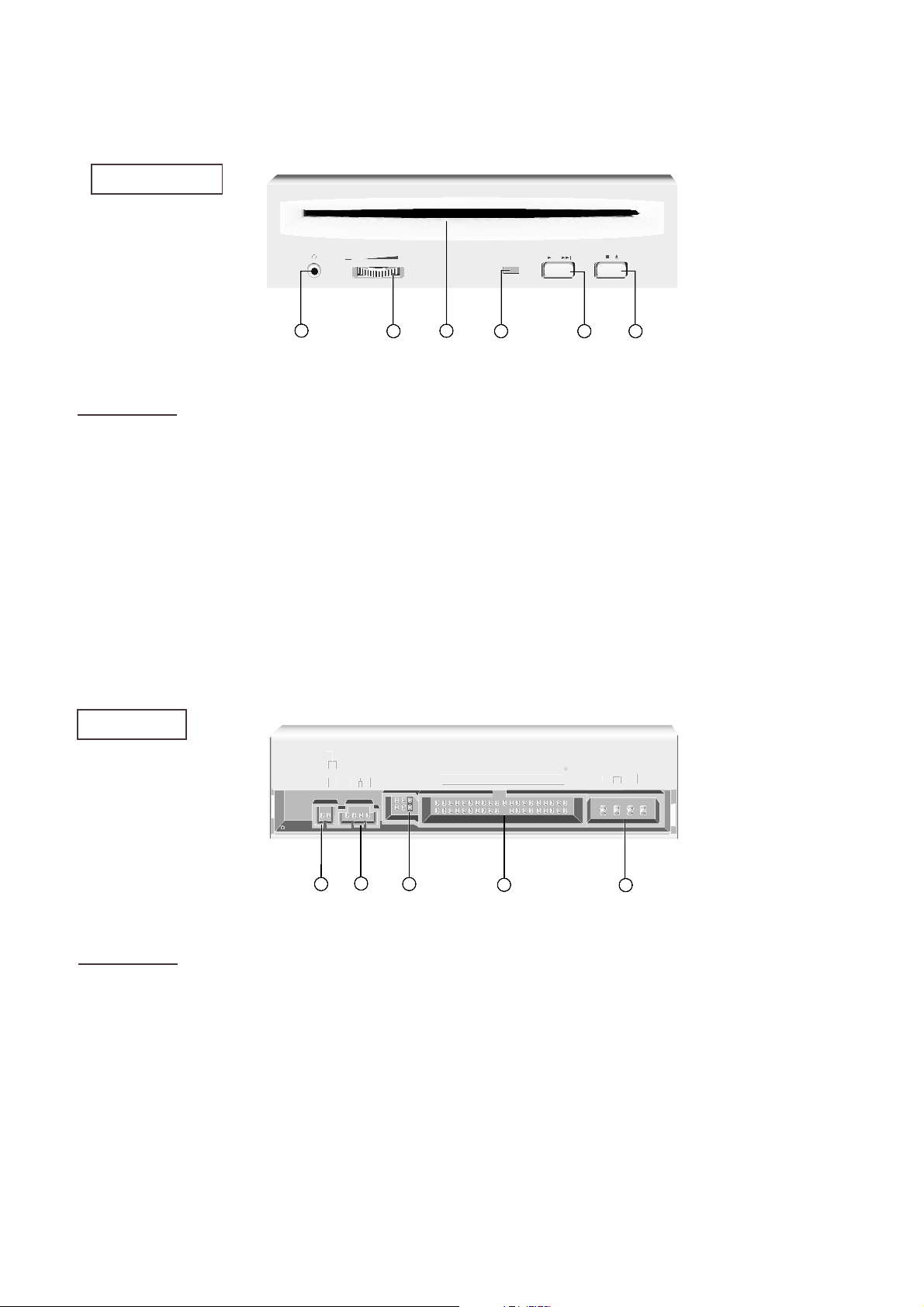
LOCATION OF CUSTOMER CONTROLS
FRONT VIEW
1. Headphone Jack
3.5mm jack for monitoring the audio signal from audio
CDs.
2. Headphone Volume Control
Adjusts the headphone sound level.
3. Disc Slot
Push a 12cm CD-ROM disc into slot.
4. Busy Indicator
The Busy Indicator lights during initialization and dataread operations.
5. Play/Skip Button
When an Audio CD is in the unit, pressing this button
will start playing audio CDs from the first track. If an
audio CD is playing, pressing this button will skip to
the next track.
6. STOP/EJECT Button
This button is pressed to eject the CD disc.
The button works only when power is applied to the
drive.
If an audio CD is playing, pressing this button will stop
it, and pressing it
again will eject the CD disc.
Figure 1. Front View
1
2 54 6
3
BACK VIEW
1. Digital Audio Ouput Connector
This is a digital audio output connector or Video CD
output connector.
You can connect this to the digital audio system or
Video CD Board.
2. Analog Audio Output Connector
The Audio Output Connector connects to a sound
card.
The supplied audio cable is a SoundBlaster
®
type
cable. If you have a different sound card, you must
optain the proper for that card.
3. Master / Slave / CSEL Jumper
These three jumpers are used to set the CD-ROM
Drive to either a Master, Slave, or CSEL drive.
4. Interface Connector
This 40-pin connector is used to transfer and control
signals between the CD-ROM Drive and your PC.
Connect the 40-pin IDE cable in your PC to this
connector.
5. Power-in Connector
Attach a power cable from the computer to this
connector.
Figure 2. Back View
DIGITAL ANALOG
INTERFACE POWER
DR CSM
SLA
GLG39 1
+5
+12
GND
40 2
AUDIO AUDIO
1
2
5
4
3
FRONT
REAR
Page 3
5
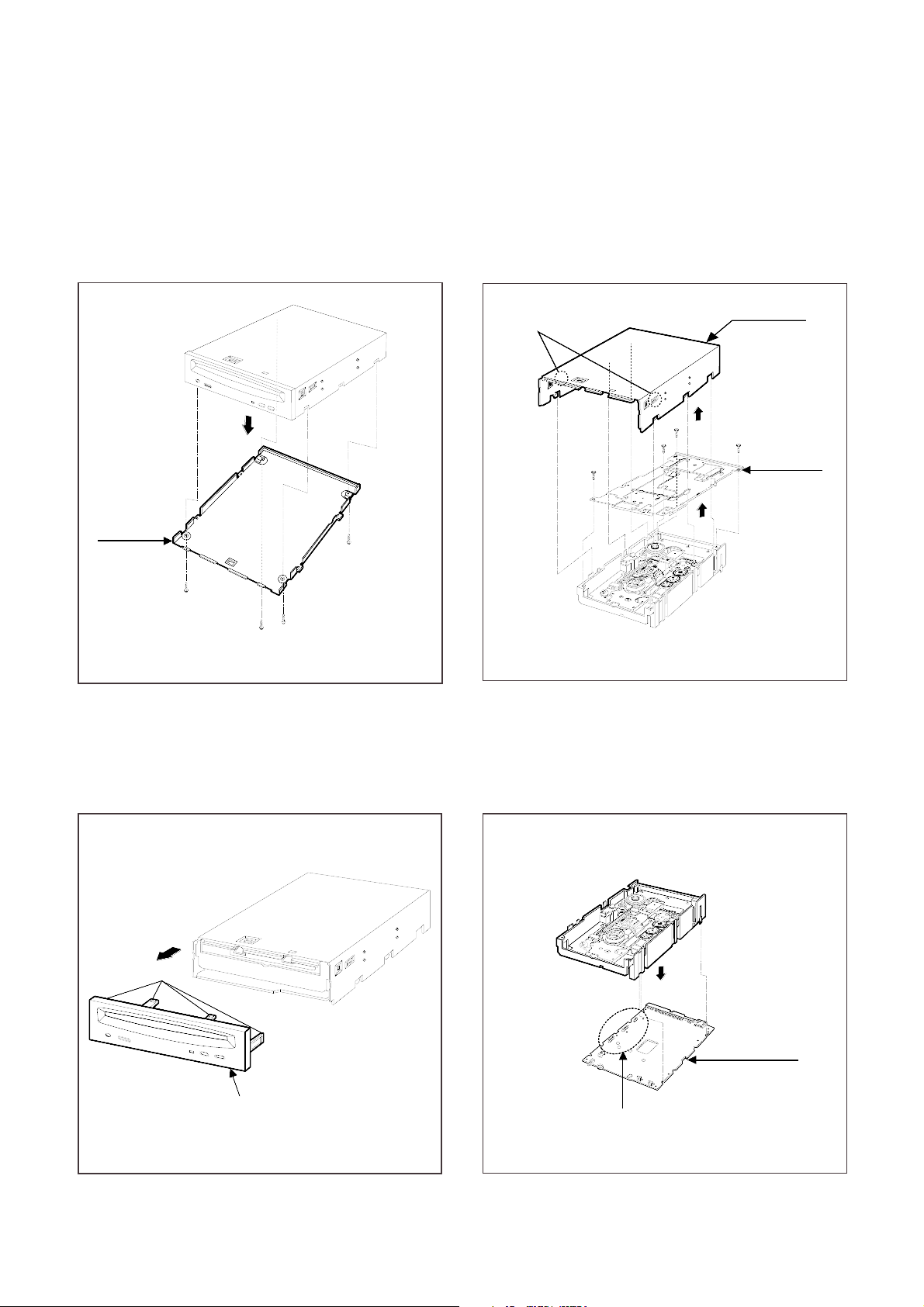
1. CABINET and CIRCUIT BOARD
DISASSEMBLY
1-1. Bottom Chassis
A. Release 4 screws (A) and remove the Bottom
Chassis in the direction of arrow (1).
(See Fig. 1-1)
1-2. Front Bezel Assy
A. Release 4 stoppers and remove the Front Bezel
Assy.
1-3. Top Case and Chassis Mecha
A. Release 2 hooks (a) and remove the Top Case in
the direction of arrow (2).
B. Release 4 screws (B) and remove the Chassis
Mecha in the direction of arrow (3)
1-4. Main Circuit Board.
A. Remove the Main Circuit Board in the direction of
arrow (4).
B. At this time, be careful not to damage the 4
connectors of the Main Circuit Board.
Bottom
Chassis
(1)
(A)
(A)
(A)
(A)
Fig. 1-1
Chassis
Mecha
Top Case
Hooks (a)
(B)
(B)
(B)
(2)
(3)
(B)
Fig. 1-3
Main
Circuit Board
4 Connectors
(4)
Fig. 1-4
Front Bezel Assy
Stoppers
Fig. 1-2
DISASSEMBLY
Page 4
6
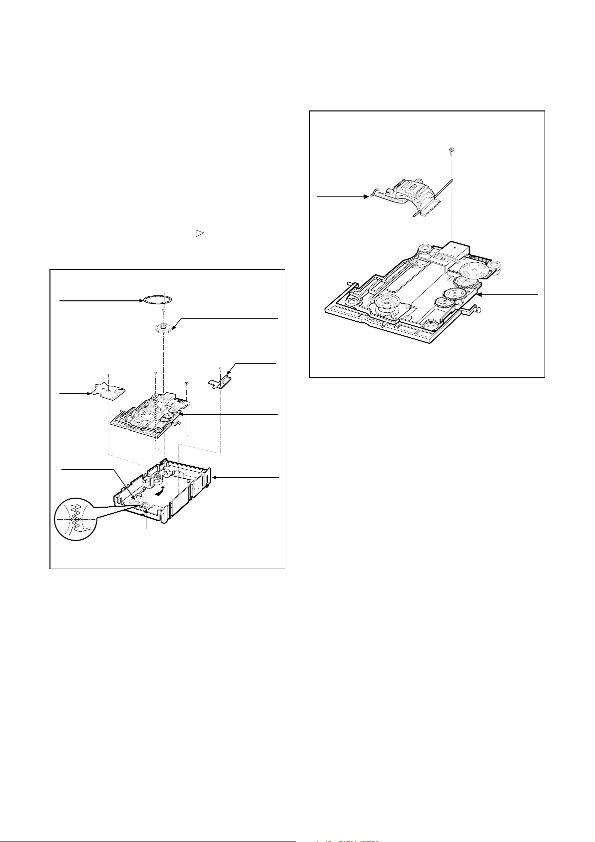
2. MECHANISM ASSY
2-1. Pick-Up Unit
A. Release 1 screw (C).
B. Remove the Loading Belt and Loading Gear.
C. Release 1 screw (D).
D. Remove the stopper (R).
E. Release 1 screw (E).
F. Remove the Elevator Cover.
G. Release 2 screws (F).
H. Remove the Pick-Up Unit in the direction of
arrow (5).
* NOTE
When reassembling the Timing Gear and the
Elevator gear, align the mark( ) of Timing Gear
with the mark(o) of Elevator Gear.
2-2. Pick-Up
A. Release 1 screw (G).
B. Remove the Pick-Up
Mechanism
Assy
Stopper(R)
Pick-UP
Unit
Elevator Gear
Loading
Gear
Elevator
Cover
Timing
Gear
Loading
Belt
(E)
(C)
(F)
(F)
(D)
(5)
Fig. 2-1
Pick-Up
Unit
Pick-Up
(G)
Fig. 2-2
Page 5
26
TROUBLESHOOTING GUIDE
1. Initial Lead-in Operation
Reset or Power-On.
LED Flikers.
Pick-Up moves to the inner-Track.
Ratate disc.
Laser on the Pick-Up lights.
Focus Search (through moving up and down the lens of Pick-Up)
Focus Servo On (FOK(TP10) : H, FEO(TP14) signal generation)
Tracking Servo On (TEO(TP13) Signal generation)
Spindle Servo On (MDP(TP17) Signal generation)
Read TOC Area (LED Flikers)
Search the Start of Data Area (00:02:16) and then pause.
2. Trouble List (Circuit)
(In the Initial Lead-in Operation Mode)
A. LED doesn’t light.
B. Pick-Up doesn’t move to the inner-track.
C. Disc doesn’t rotate.
D. The Laser (RED) of Pick-Up doesn’t light.
E. Pick-Up lens doesn’t move up and down.
F. TOC isn’t read. (The state LED is not disappear.)
(In the Operation Mode)
G. Jump is unstable (Noises are occurred.)
H. During the Access, Pick-Up slides innermost track or outermost track.
I. High speed operating (8~16 times) is performed, but normal speed (1 time: Audio CD) operating is
unstable.
J. During Audio CD Play, LED flickers, but Speaker is silent.
K. Trouble for compatibility.
Page 6

27
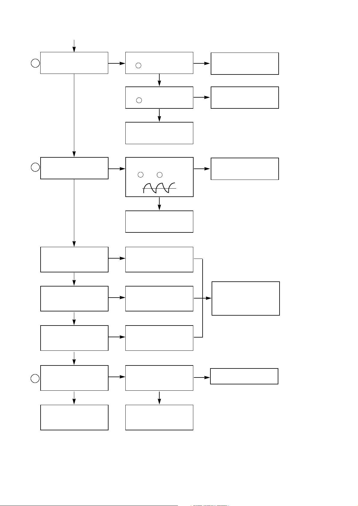
3. Troubleshooting Guide (In the Initial Lead-in Operation Mode)
Reset or Power On.
Check Power Voltage,
Reference Electrical Potential
and GND.
Does LED light?
Does Pick-Up move to
the inner track?
Does “H” output in IC401
pin ?
Is the CLOCK Frequency
of X401 16.93MHz?
Check and replace R318,
R323, Q307 and LD301.
Does the signal appear in
the IC401 pin , ?
Replace IC401
Replace IC401
Does Disc rotate?
Does the signal appear
in the FOK(TP10),
IC501 pin ?
Replace IC501
Replace IC501
Replace IC501
Replace IC201
Does the signal appear in
the TP1, TP2?
Replace IC203
Replace MD Assy.
(Sled Motor is defective.)
Replace
X401.
YES
YES YES
YES
YES
YES
YES
YES
YES
YES
YES
NO NO NO
NO
NO
NO
NO
NO
NO
NO
NO
A
B
C
48
45
106
46
Dose the signal appear
in the MDP(TP17),
IC501 pin ?
Does the signal appear in
IC203 pin (A3),
(A2) and (A1)?
Replace MD Assy.
Does the signal appear in
IC501 pin ?
FEO
SENS
95
115
4
2
7
Page 7
28
Does the Laser (RED
light) of Pick-Up light?
Does “H” output in IC102
pin ?
Replace IC401
YES
YES
YES
YES
YES
YES YES
YES
YES
YES
NO
NO
NO
25
Does the Pick-Up lens
move up and down?
Does the focus search
signal appear between
pin and of IC203?
Replace IC203
NONO
Is the Focus Servo On?
(Does FEO(TP14) signal
appear?)
NO
30
31
Is the Voltage of IC102
pin (LD) 2.2V?
Replace IC102
Replace MD Assy
(Laser Diode of the
Pick-Up is defective.)
Replace MD Assy
(Focus actuater coil of the
Pick-Up is defective.)
Focus Servo is unstable
Is the Tracking Servo
On? (Does TEO(TP13)
signal appear?)
NO
Tracking Servo is
unstable
Replace IC501,
MD Assy or Main Circut
Board.
Is the Spindle Servo On?
(Does MDP(TP17) Signal
appear?)
NO
Spindle Servo is unstable.
Is TOC area on the Disc
read? (Does LED flicker?)
NO NO
Does the other Disc
operate normally?
Disc is defective.
The End.
Replace Main circuit
Board or MD Assy.
D
E
1
F
Page 8
29
4. Troubleshooting Guide (In the Operation Mode)
When the jump is unstable (Noise occurs);
(1) Readjust the Slide Motor offset.
(2) Replace Main Circuit Board or MD Assy.
When the Pick-Up slides to innermost track or outermost track during the Access;
(1) Replace MD Assy.
When the High Speed operating (8~16 times) is performed, but normal speed operating (1 time) for
Audio CD is unstable;
(1) Perform Down Load again.
(Refer to Owner’s Manual)
(2) Replace MD Assy.
During Audio CD play, LED flickers, but Speaker is silent;
When the headphon volume is not controlled;
(1) Replace VR301
Others (Video CD is not played, screen is abnormal or some title is not played.)
: Troubles for Compatibility
5. When the data read failure of CD-ROM Disc
(1) Check the CD-ROM Disc.
(2) Check the IC's in the decoder and interface circuit.
a) DRAM : IC601
b) CD-ROM Decoder & E-IDE Controller : IC602
c) Microprocessor : IC401
G
H
I
J
J-1
K
Does PWM signal appear
in IC501 pin ?
Replace IC501.
YES
NO
82
83,91,92
,
Does Audio signal appear
in IC301 pin ?
Replace IC301.
YES
NO
1
7
,
Are L-CH and R-CH
signals appeared in
JK301 and JK302 each?
Replace L310, L311.
YES
NO
Is the connection between
JK301(or JK302) and Line
(or Jack) normal?
Normal.
Speaker is defective.
YES
NO
Page 9

30
6. Write I/F Signal Flow (Drive << Host)
Above figure is timing flow presented data transfer from Host to Drive.
And, the followings are those conditions;
1. When the Host write the ATAPI packet command-word
2. When the Host write the Data (ex, Mode select command) - word
3. When the Host write the task file registers - byte
Now, the corresponding register is chosen by control signal HCSO, HCSI, HA [2:0] and the Host write the
command (or Data) through the corresponding register.
To write some words (or bytes), the IOW (IO write signal) must be active - low, that is, the actual Data (HD
[15:0]) will be loaded by the synchronized IOW signal (active-low).
*IOCS16 : depends on the quantity of Data (word or byte), that is, if word, that signal was enabled.
*IORDY : depends on the transfer rate of Host.
Dn-3 Dn-2 Dn-1 DnD0 D1
≈
≈
≈
≈
≈
≈
7. Read I/F Signal Flow (Drive >> Host)
Above figure is timing flow presented data transfer from Drive to Host.
And, the followings are those conditions;
1. When the Host read the data from Drive (ex, Read command) - word
2. When the Host read the task file registers - byte
Above timing sequence is similar with the previous write timing sequence.
Only different thing is that the IOW is substituted by IOR (IO read signal)
that is, the actual data will be loaded by the synchronized IOR signal (active -low).
Dn-3 Dn-2 Dn-1 DnD0 D1
HA [2:0]
HCS0, HCS1
IOR
HD [15:0]
IOCS16
IORDY
≈
≈
≈
≈
≈
≈
Page 10

13
IC INTERNAL BLOCK DIAGRAM AND PIN DESCRIPTION
IC102 (CXA2556Q) : RF Amplifier IC
I-V convertes and amplifies the signal by receiving, from the Pick-up, and than applies to DSP &
SSP IC (IC501).
Block Diagram
1
32
31
2
3
4
5
6
7
8
910
11
12
13 14
15
17
16
18
19
20
21
22
23
24
25
2627
28
29
30
BOOST
CONTROL
FILTER
CONTROL
VCR
CONTROL
MODE
SW
VCRLPFMIXER
DELAY
LPF
HPF
BOOST
VS
VC
Vcc
44p
HOLD
PEAK
/BOT
VCR
VCR
LD
PD
A
B
C
D
GND
NC
GND
E
FE B
FE
TE C
TE
TE1
F
MIRR T
CP
MIRR
Vcc
RFO 2
RFO 1
MODE 2
MODE 1
RFO
RFI
SUM OUT
EQ IN
RF C
BST C
FC C
APC ON
VC
VC
VC
VC
VC
VC
VC
VC
18k
44k
39k
80k
80k
80k
80k
22k
51k
Vcc
1.25V
MODE1
10P
APC ON
56k
1k
56k
1.25V
10k
10k
10k
55k
10k
40k
40k
40k
40k
73.34k
2p
320k
32k
32k
32k
32k
20k
1.25V
40k
20k
164k
40k
87k
40k
40k
Vcc
Vcc
20k
187k
18.3p
Page 11

IC102 CXA2556Q
Pin Description
14
Pin No. Symbol I/O Description
1 LD O APC Amp output
2 PD I APC Amp Intput
3 A I RF Summing Amp,
4 B I Focus Error Amp Input
5C I
6D I
7 GND GND
8 NC No Connect
9 E I Tracking Error Amp Input. (9, 10)
10 F I
11 TEI O Tracking Error Amp Output. (11)
12 TEC I Control Tracking Error Low Frequency Gain (12)
13 TE O Tracking Error Amp Output (13)
14 FEB O Adjust Focus Bias
15 FE O Focus Error Amp Output
16 VC O (Vcc+GND)/2
17 MIRR T I Control Peak Hold Value
18 CP I Mirror Hold Capacitor Input
Mirror Comparator non Invertor Input
19 MIRR O Mirror Comparator Output
20 Vcc Vcc
21 RFO2 O Buffer Switch Output (Control in 23 and 24 pin)
22 RFO1 O RF Equalizer Output
23 MODE 2 I
24 MODE 1 I
25 APC ON I APC Amp on /off Switching
26 FCC I RF Equalizer LPF Cutoff Frequency Setting Pin
27 BSTC I RF Equalizer High Frequency Boost Setting Pin
28 RFC I RF Amp, RF Equalizer Low Frequency Gain Setting Pin
29 EQIN I RF Equalizer Input
30 SUMOUT O RF Summing Amp Invertor output
31 RFI I Mirror Circuit Input
32 RFO O RF Signal Output
MODE 1 MODE 2
x1 GND GND
xN Vcc GND
x1.5N GND Vcc
x2.0N Vcc Vcc
Control Velocity
Page 12

15
IC201 (BA6849FP) : Spindle Drive IC
Controls the Spindle Motor by receiving MDP signal from DSP (IC501).
Block Diagram
SB
SHORT BRAKE
1
2
4
7
8
10
11
12
13
14
15
17
20
21
22
24
25
26
27
28
9
DRIVER
GAIN
CONTROL
A3
A2
A1
Hall 1
Hall 2
Hall 3
GND
H1+
H1-
H2+
H2-
H3+
H3-
HALL AMP
+
+
+
_
_
+
+
_
_
_
+
_
+
_
R
D
Q
QCK
Hall Bias
FIN
R
NF
RNF
VM
Vcc2
Vcc1
PG
PS
EC
ECR
FR
CNF
VH
PS
TORQUE
SENSE AMP
Vcc
Vcc1
SERVO
SIGNAL
V
M
CURRENT
SENSE AMP
TSD
Vcc
TL
23
RNF
VM
VCC2
V
CC1
PGPSEC
E
CRGND
H
1
+
H
2
+
H
1
H
2
H
3
+
H
3
-
FR
N.CSBC
NF
VH
N.C.
1
2
3
4
5
6
7
8
9
10
11
121314
15
16
17
18
19
20
21
22
23
24
25
26
27
28
A3
A2
A1
N.C.
N.C.
N.C.
BA6849FP
Page 13

IC203 (M56759FP) : Servo Actuator Drive IC
Generates the signal to rotate Focus Actuator Coil,Tracking Actuator Coil and Sied Motor by PWM
Error Signal input from DSP.
Block Diagram
PWM2
R1
R2
VREFOVREFO
VREFO
VCTL3
PWM2
PWM1
FOCUS
TRACKING
C1
R1
PWM1
MUTE2
ch4
ch2
ch3
ch1
MUTE1
OUT1VM1+
Vm1
VCC1
GND
VM2-VM2+
OUT2
IN2-
IN2+
SIN2-
SOUT2
OP1+
OP1-
OP2- OP2+
Vm3
IN3+
IN3-
VM3-
VCC2
VM4-
VM4+ IN4A-
IN4B-
Vm2 VREF VREF0VM3+
OUT3
OP1OUT
OP2OUT
T S D
VM1-
SOUT1
SIN1-
IN1+
IN1-
R2
5V
C2
C2
R4
R3
R3
R4
C1
5k
5k
5k
10k
10k
10k
10k 12.5k
12.5k
12.5k
12.5k
5k
5k
10k
10k
5k
5k
2.5k
2.5k
2.5k
2.5k
2.5k
12.5k
12.5k
12.5k
12.5k
12.5k
2.5k
12.5k
2.5k
12.5k
2.5k
4k
25k
12.5k
10k 10k
12V
5k
5k
10k
10k
10k
12V
10k
5k
_
-
--
--
-
-
-
-
-
-
-
+
+
+
+
+
+
+
+
-
+
+
+
+
+
-
+
+
-
+
-
-
-
+
+
+
VCTL4
TRAY
TRAVERSE
M
M
1
2
345
678
9
1011121314151617181920
21
424140393837363534333231302928272625242322
VCC2
VREF
VREF0
IN3-
IN3+
Vm3
OUT3
VM3(-)
VM3(+)
GND
VM4(+)
VM4(-)
IN4A-
Vm2
IN4B-
OP1OUT
OP1-
OP1+
OP2+
OP2-
MUTE2
MUTE1
SOUT2
SIN2-
IN2+
IN2-
OUT2
VM2(-)
VM2(+)
VM1(+)
VM1(-)
OUT1
IN1-
IN1+
Vm1
SIN1-
SOUT1
V
CC1
OP2OUT
GND
M56759FP
16
Page 14

17
IC401 (M8-3396) : µ-COM
Controls all Drive systems by input and output the Data from the peripheral IC.
IC501 (CXD3000R) : DSP & SSp
Generates Error Signal and return to the Servo by the Signal from RF Amplifier IC.
108 107 106 105 104 103 102 101 100 99 98 97 96 95 94 93 92 91 90 89 88 87 86 85 84 83 82 81 80 79 78 77 76 75 74 73
NCNCFOK
DFCT
MIRR
COUT
DV
SS
4
CLOK
XLAT
DATA
ATSK
SCLK
DIRC
SENS
DV
DD
4
AV
DD
3
AO1R
AO1FNCAV
SS
3
AV
SS
5
XTLI
XTLO
AV
DD
5
AV
DD
4
AO2F
AO2R
AV
SS
4
DA
SS
3
DAS1
DAS0
XWO
DTS0
DTS1NCNC
NC
NC
TESTA
PWMI
FSW
MON
MDP
MDS
LOCK
SSTP
DV
SS
5
SFDR
SRDR
TFDR
TRDR
FFDR
FRDR
DV
SS
5
NC
VCOO
VCOI
TEST
TES2
TES3
PDO
VCKI
V16M
AV
DD
2
IGEN
AV
SS
2
ADIO
RFDC
CE
TE
NC
NC
1 2 3 4 5 6 7 8 9 10 11 12 13 14 15 16 17 18 19 20 21 22 23 24 25 26 27 28 29 30 31 32 33 34 35 36
NC
NC
SE
FE
VC
VPCO1
VPCO2
VCTL
FILO
FILI
PCO
CLTV
AV
SS
1
RFAC
BIAS
ASYI
ASYO
AV
DD
1
NC
DV
DD
1
DV
SS
1
ASYE
PSSL
WDCK
LRCK
LRCKI
DA16
PCMDI
DA15
BCKI
DA14
DA13
DA12
DA11
NC
NC
110
111
112
113
114
115
116
117
118
119
120
121
122
123
124
125
126
127
128
129
130
131
132
133
134
135
136
137
138
139
140
141
142
143
144
109
NC
NC
DTS2
XRST
SCSY
SQCK
SQSO
EXCK
SBSO
SCOR
WFCK
MUTE
DOUT
MD2
DV
DD
3
C16M
C4 M
FSTO
NC
FSTI
MCKO
XTSL
DV
SS
2
DA01
DA02
DA03
DA04
DA05
DA06
DV
DD
2
DA07
DA08
DA09
DA10
NC
NC
71
70
69
68
67
66
65
64
63
62
61
60
59
58
57
56
55
54
53
52
51
50
49
48
47
46
45
44
43
42
41
40
39
38
37
72
CXD3000R
Page 15

18
IC501 CXD3000R
Block Diagram
86 87
6 7
51 75 70 77
78 79
28 30 26
91
92
83
82
23
61
60
59
99
95
103
104
105
106
120
121
69
138
13
21
136
1820
132131
130139
5
4
3
141
142
140
112
116
115
113
114
67
66
64
65
63
22
62
17
16
14
9
10
11
128
129
52
134
135
56
55
8
57
133
122
123
124
125
101
100
XTLO
XTLI
VPCO1
VPCO2
XTSL
DTS1
DTS2
XWO
DAS0
DAS1
PCMDI
BCKI
LRCKI
MCKO
V16M
VCKI
FSTO
C4M
C16M
VCTL
PDO
VCOI
PCO
VCOO
FILI
FILO
CLTV
RFAC
ASYI
ASYO
ASYE
WFCK
SCOR
EXCK
MON
SQCK
SQSO
SBSO
FSW
MDP
MDS
PWMI
RFDC
CE
TE
SE
FE
VC
ADIO
TEST
TES2
TES3
A/D
CONVERTER
OpAmp
AnaSw
Clock
Generator
4fs Digital Filter
1 bit DAC
+
32K RAM
DAC BLOCK
AO1F
AO1R
AO2F
AO2R
Error
corrector
CLV
processor
Timing
Generator 2
SIGNAL PROCESSOR BLOCK
SERVO BLOCK
OSC
Digital PLL
Vari-Pitch
double speed
EFM
Demodulator
Timing
Generator 1
Subcode
P-W
Processor
Subcode Q
Processor
Noise
Shaper
18-times
oversampling
filter
Servo
interface
MIRR
DFCT
FOK
Register
Address
generator
Priority
encoder
D/A data
processor
Peak
detector
Digital out
Serial/parallel
Processor
PSSL
MUTE
DOUT
MD2
DATA
CLOK
XLAT
SENS
COUT
MIRR
DFCT
FOK
SFDR
SRDR
TFDR
TRDR
FFDR
FRDR
PWM GENERATOR
FOCUS PWM
GENERATOR
TRACKING PWM
GENERATOR
SLED PWM
GENERATOR
DV 0
DD
DV 1
DD
AV 1
DD
AV 2
DD
AV 3
DD
AV 4DDAV 5
DD
DV 0
SS
DV 1
SS
AV 1
SS
AV 2
SS
AV 3
SS
AV 4SSAV 5
SS
XRST
SERVO DSP
FOCUS SERVO
TRACKING SERVO
SLED SERVO
CPU interface
Servo
auto
sequencer
8
DA01
DA16
~
29, 27
~
~
12
MUX
49 44,
42 31,
Sync
protector
124
123
122
121
120
106
105
104
103
Page 16

IC501 CXD3000R
Pin Description
19
Pin No. Symbol I/O Description
3 SE I Slide Error input
4 FE I Focus Error input
5 VC I Center voltage input
6 VPCO1 O 1, Z, 0 Output of VCO2 charge pump for vari-pitch PLL
7 VPCO2 O 1, Z, 0 Output 2 of VCO2 charge pump for vari-pitch PLL
8 VCTR I Input of VCO2 control voltage for vari-pitch EFM
9 FILO O Analog Output of Filter for master PLL (slave = digital PLL)
10 FILI I Input to filter for master PLL
11 PCO O 1, Z, 0 Output of charge pump for master PLL
12 CLTV I VCO control voltage lnput for master PLL
13 A V
SS1 Analog GND
14 RFAC I EFM signal input
15 BIAS I Asymmetry circuit constant current input
16 ASYI I Asymmetry comparator circuit voltage input
17 ASYO O 1, 0 EFM full-swing output
18 A V
DD1 Analog power supply
20 D V
DD1 Digital power supply
21 D V
SS1 Digital GND
22 ASYE I Asymmetry circuit ON/OFF (L=OFF, H=ON)
23 PSSL I Input used to switch the audio data output mode. (L=serial, H=parallel)
24 WDCK O 1, 0 D/A interface for 48-bit slot. Word clock f=2Fs
25 LRCK O 1, 0 D/A interface for 48-bit slot. LR clock f=Fs
26 LRCKI I LR clock input to DAC (48-bit slot)
27 DA16 O 1, 0 Outputs DA16 (MSB) when PSSL=1, or serial data from the 48-bit slot (2's complements,
MSB first) when PSSL=0.
28 PCMDI I Audio data input to DAC (48-bit slot)
29 DA15 O 1, 0 Outputs DA15 when PSSL=1, or bit clock from the 48-bit slot when PSSL=0.
30 BCKI I Bit clock input to DAC (48-bit slot)
31 DA14 O 1, 0 Outputs DA14 when PSSL=1, or serial data from the 64-bit slot (2's complements,
LSB first) when PSSL=0.
32 DA13 O 1, 0 Outputs DA13 when PSSL=1, or bit clock from the 64-bit slot when PSSL=0.
33 DA12 O 1, 0 Outputs DA12 when PSSL=1, or LR clock from the 64-bit slot when PSSL=0.
34 DA11 O 1, 0 Outputs DA11 when PSSL=1, or GTOP when PSSL=0.
39 DA10 O 1, 0 Outputs DA10 when PSSL=1, or XUGF when PSSL=0.
40 DA09 O 1, 0 Outputs DA9 when PSSL=1, or XPLCK when PSSL=0.
Page 17

20
Pin No. Symbol I/O Description
41 DA08 O 1, 0 Outputs DA8 when PSSL=1, or GFS when PSSL=0.
42 DA07 O 1, 0 Outputs DA7 when PSSL=1, or RFCK when PSSL=0.
43 DV
DD2 Digital Power supply
44 DA06 O 1, 0 Outputs DA6 when PSSL=1, or C2PO when PSSL=0.
45 DA05 O 1, 0 Outputs DA5 when PSSL=1, or XRAOF when PSSL=0.
46 DA04 O 1, 0 Outputs DA4 when PSSL=1, or MNT3 when PSSL=0.
47 DA03 O 1, 0 Outputs DA3 when PSSL=1, or MNT2 when PSSL=0.
48 DA02 O 1, 0 Outputs DA2 when PSSL=1, or MNT1 when PSSL=0.
49 DA01 O 1, 0 Outputs DA1 when PSSL=1, or MNT0 when PSSL=0.
50 DV
SS2 Digital GND
51 XTSL I X'tal selection input
52 MCKO O 1, 0 Clock output. Inverse output of XTLI
53 FSTI I 2/3 frequency demultiplication input of MCLK
55 FSTO O 1, 0 2/3 frequency demultiplication output. Unaffected by vari-pitch
56 C4M O 1, 0 1/4 frequency demultiplication output. Affected by vari-pitch
57 C16M O 1, 0 16.9344MHz output. Subject to vari-pitch control.
58 DV
DD3 Digital power supply
59 MD2 I Digital-Out ON/OFF control. "H" for ON, "L" for OFF.
60 DOUT O 1, 0 Digital-Out output.
61 MUTE I "H" for muting, "L" for release.
62 WFCK O 1, 0 WFCK (Write Frame Clock) output.
63 SCOR O 1, 0 "H" when subcode Sync S0 or S1 is detected.
64 SBSO O 1, 0 Serial output of Sub P to W
65 EXCK I Clock input for reading SBSO
66 SQSO O 1, 0 Outputs 80-bit Sub Q and 16-bit PCM peak-level data.
67 SQCK I Clock input for reading SQSO
68 SCSY I Input of GRSCOR
69 XRST I System reset. "L" for resetting
70 DTS2 I Test pin for DAC. Normally "H"
75 DTS1 I Test pin for DAC. Normally "H"
76 DTS0 I Test pin for DAC. Normally "L"
77 XWO I Window open input for DAC synchronization. generally, at "L" window open
78 DAS0 I Test pin for DAC. Normally "H"
79 DAS1 I Test pin for DAC. Normally "L"
80 DV
SS3 Digital GND
81 DV
SS4 Analog GND
82 AO2R O 1, 0 CH2•DAC•PWM output (reverse phase)
Page 18

21
Pin No. Symbol I/O Description
83 AO2F O 1, 0 CH2•DAC•PWM output
84 AV
DD4 Analog power supply
85 AV
DD5 Power supply for master clock
86 XTLO O 1, 0 X'tal oscillation circuit output of master clock.
87 XTLI I X'tal oscillation circuit input of master clock.
88 AV
SS5 GND for master clock
89 AV
SS3 Analog GND
91 AO1F O 1, 0 CH1•DAC•PWM output
92 AO1R O 1, 0 CH1•DAC•PWM output (reverse phase)
93 AV
DD3 Analog power supply
94 AV
DD4 Digital power supply
95 SENS O 1, Z,0 SENS output
96 DIRC I For 1 track jump
97 SCLK I Clock for SENS serial data
98 ATSK I Pin for Anti-shock
99 DATA I Digital Data input from CPU
100 XLAT I Latch input from CPU
101 CLOK I Serial Data transfer clock input from CPU
102 DV
SS4 Digital GND
103 COUT O 1, 0 Track number count signal output
104 MIRR O 1, 0 Mirror signal output
105 DFCT O 1, 0 Defect signal output
106 FOK O 1, 0 Focus OK output
111 TESTA Test pin
112 PWMI I Input of spindle control
113 FSW O 1, Z, 0 Output used to switch the spindle motor output filter.
114 MON O 1, 0 Output for spindle motor ON/OFF control
115 MDP O 1, 0 Output for spindle motor servo control
116 MDS O 1, 0 Output for spindle motor servo control
117 LOCK O 1, 0 Output is "H" when the GFS signal sampled at 460Hz is "H". Output is "L" when the
GFS signal is "L" 8 or more times is succession.
118 SSTP I Disc inner periphery detection signal input
119 DV
SS5 Digital GND
120 SFDR O 1, 0 Slide drive output
121 SRDR O 1, 0 Slide drive output
122 TFDR O 1, 0 Tracking drive output
Page 19

Notes :
• The data at the 64-bit slot is output in 2's complements on an LSB-first basis. The data at the 48-bit slot is
output in 2's complements on an MSB-first basis.
• GTOP monitors the state of Frame Sync protection. ("H" : Sync protection window released)
• XUFG is a negative Frame Sync pulse obtained from the EFM signal before Frame Sync protection is
effected.
• XPLCK is an inversion of the EFM PLL clock. The PLL is designed so that the falling edge of XPLCK
coincides with a change point of the EFM signal.
• The GFS signal turns "H" upon coincidence between Frame Sync and the timing of interpolation protection.
• RFCK is a signal generated at 136-µs periods using a crystal oscillator.
• C2PO is a signal to indicate data error.
• XRAOF is a signal issued when a jitter margin of +28F is exceeded by the 32K RAM.
22
Pin No. Symbol I/O Description
123 TRDR O 1, 0 Tracking drive output
124 FFDR O 1, 0 Focus drive output
125 FRDR O 1, 0 Focus drive output
126 DV
DD5 Digital power supply
128 VCOO O 1, 0 Output of oscillation circuit analog EFM PLL
129 VCOI I Input to oscillation circuit for analog EFM PLL. f
LOCK=8.6436MHz
130 TEST I Test Pin. Normally "L"
131 TES2 I Test Pin. Normally "L"
132 TES3 I Test Pin. Normally "L"
133 PDO O 1, Z, 0 Output of charge pump for analog EFM PLL
134 VCKI I Clock input from external VCO for vari-pitch control. fc
center=16.9344MHz
135 V16M O 1, Z, 0 Output of VC02 oscillation for vari-pitch EFM PLL
136 AV
DD2 Analog power supply
137 IGEN I Resistor connection pin of current source reference for OP Amp
138 AV
SS2 Analog GND
139 ADIO O OP Amp output
140 RFDC I RF signal input
141 CE I Center servo analog input
142 TE I Tracking error signal input
Page 20

23
IC602 (OTI-911LP) : I/F and Decoder IC
Applies the order from the PC to µ-COM, and transmittes the input Signal from DSP to PC with Data.
Block Diagram
HDR/SUBHDR
Ragisters
Status/Control
Registers
CD-DSP
Address
Counters
CD-DSP
Subcode
I/F Logic
uP
Data
Xfer
EDC
CRC
Check
R-S
ECC
Data
Corr
ECC
EDC
Addrs
Gen
CD-DSP I/F
LOGIC
Data Path
Control
System
Controller
CD-DSP
IDE
Register
IDE
Register
12-Bytes
FIFO
IDE
Shadow
Register
Control
DRAM
Control
RAD(15:0)
RD(7:0)
DRAM
Host Control
IDE
BUS
Host/uP
Address
Counters
DD(15:8)
DD(7:0)
CNTRL
HA(2:0)
UD(7:0)
OTI-911
VSSE 1
RAD3 2
RAD11 3
ALE/RAD13 5
RAD15 6
VSSE 7
DLRCK 8
RAD12 4
DSDATA 9
DBCK 10
DC2PO 11
MCK 13
XOUT 14
XIN 15
VSSI 16
DJPAR 12
SBSO 17
WFCK 18
SUB 19
HRST- 21
UD0 22
VSSE
23
UD1
24
EXCK 20
RD3
81
RD2
82
RAD10
83
RD0
85
VSSE
86
RD1
87
RWE-88ROE-
84
VDD
89
RAD14
90
RAD9
91
RAD7
93
VSSE
94
RAD6
95
RAD596RAD8
92
RAD4
97
RAD0
98
RAD1
99
RAD2
100
31
HRD-
32
IORDY
33
DMACK-
35
VSSE
36
IOCS16-
37
HA1
38
HPDIAG-
34
HIRQ
39
HA0
40
VDD
41
HA2
43
CS3FX-
44
HDASP-
45
UINT-
46
UCS-
42
CS1FX-
47
UWR-
48
URD-
49
URS
50
UD7
UD2 25
UD3 26
UD4 27
UD6 29
VSSE 30
UD5 28
80
VSSE
79
RD6
78
RD7
76
RD4
75
PRST-
74
HD7
73
HD8
77
RD5
72
VSSE
71
HD6
70
HD9
68
HD10
67
HD4
66
VSSE
65
HD11
69
HD5
64
VSSI
63
HD3
62
HD12
60
ARST-
59
HD13
58
VSSE
57
HD1
61
HD2
56
HD14
55
HD0
54
HD15
52
HWR-
51
VSSE
53
HDRQ
OAK
OTI-911
Page 21

24
IC 602 OTI-911LP
Pin Description
Pin No.
1
2
3
4
5
6
7
8
9
10
11
12
13
14
15
16
17
18
19
20
21
22
23
24
25
26
27
28
Pin No.
29
30
31
32
33
34
35
36
37
38
39
40
41
42
43
44
45
46
47
48
49
50
51
52
53
54
55
56
Name
VSSE
RAD3
RAD11
RAD12
ALE/RAD13
RAD15
VSSE
DLRCK
DSDATA
DBCK
DC2PO
DJPAR
MCK
XOUT
XIN
VSSI
SBSO
WFCK
SUB
EXCK
HRST-
UD0
UD1
VSSE
UD2
UD3
UD4
UD5
Name
UD6
VSSE
UD7
URS
URD-
UWR-
UCS-
UINT-
HDASP-
CS3FX-
CS1FX-
HA2
VDD
HA0
HPDIAG-
HA1
IOCS16-
VSSE
HIRQ
DMACK-
IORDY
HRD-
VSSE
HWR-
HDRQ
HD15
HD0
HD14
Type
P
O
O
O
I/O
*
O
P
I
I
I
I
I/O
*
O
O
I
P
I
I
I
I/O
I
I/O
I/O
P
I/O
I/O
I/O
I/O
Type
I/O
P
I/O
I
I
I
I
O
I/O
I
I
I
P
I
I/O
I
O
(1)
P
O
(2)
I
O
I
P
I
O
(2)
I/O
I/O
I/O
Comments
RAM Address Bus
ALE (RAM Address
BUS)
RAM Address Bus
44.1kHz L/R Strobe
Serial Data
Serial Bit Clock
C2 Pointer Input
Drive Jumper/
RAM Parity Data
M Clock
X'tal OSC Output
X'tal OSC Input
Subcode Interface
IDE Host Reset
uCOM Data Bus
uCOM Data Bus
Comments
uCOM Data Bus
uCOM Data Bus
uCOM Register Select
uCOM Read Strobe
uCOM Write Strobe
uCOM Chip Select
uCOM Interrupt
IDE Host Insterface
Host Address
IDE Host Interface
16 bit I/O
Host Interrupt
Host DMA Acknowledge
Host IO Ready
Host Read Strobe
IDE Host Interface
IDE Host Data Bus
Page 22

25
Pin Types: P = Power, I = Input, O = Output, I/O = Input/Output
* I/O function is selectable. See Pin description for more details.
Notes :
1. Open Drain
2. Three State
Pin No.
57
58
59
60
61
62
63
64
65
66
67
68
69
70
71
72
73
74
75
76
77
78
Name
HD1
VSSE
HD13
ARST-
HD2
HD12
HD3
VSSI
HD11
VSSE
HD4
HD10
HD5
HD9
HD6
VSSE
HD8
HD7
PRST-
RD4
RD5
RD7
Type
I/O
P
I/O
O
(1)
I/O
I/O
I/O
P
I/O
P
I/O
I/O
I/O
I/O
I/O
P
I/O
I/O
I
I/O
I/O
I/O
Comments
IDE Host Data Bus
IDE Host Data Bus
ATAPI Reset
IDE Host Data Bus
IDE Host Data Bus
IDE Host Data Bus
VSSE
IDE Host Data Bus
Chip Reset
RAM Data Bus
Pin No.
79
80
81
82
83
84
85
86
87
88
89
90
91
92
93
94
95
96
97
98
99
100
Name
RD6
VSSE
RD3
RD2
RAD10
ROE-
RD0
VSSE
RD1
RWE-
VDD
RAD14
RAD9
RAD8
RAD7
VSSE
RAD6
RAD5
RAD4
RAD0
RAD1
RAD2
Type
I/O
P
I/O
I/O
O
(1)
I/O
I/O
P
I/O
O
P
O
O
O
O
P
O
O
O
O
O
O
Comments
RAM Data Bus
RAM Data Bus
RAM Address Bus
RAM Read Enable
RAM Data Bus
RAM Data Bus
RAM Write Enable
RAM Address Bus
RAM Address Bus
Page 23

12
PHOTO DIODE STRUCTURE OF THE PICK-UP
1. Focus Error Signal => (A+C)-(B+D)
(Control the Pick-up’s up and down to focus on the Disc)
2. Tracking Error Signal => (E-F)
(Control the Pick-up’s left and right shift to find the track on the Disc)
3. RF Signal => (A+B+C’)=(A+B+C+D)
(
RF Signal is converted to Data Signal in DSP IC (IC501))
Three signals (Focus Error Signal, Tracking Error Signal and RF Siganl) above are I-V converted and
amplified at the IC102, and than are transmitted to DSP & SSP IC (IC501) to generate the Servo Control
Signal and Data Signal.
E
F
A
B
C'
Laser spot
Red laser
Pick-Up module
Tracking
Focusing
* C ’=C+D
Page 24

32
DISC MOTOR
UNIT
SPINDLE
MOTOR
BA6849
MOTOR DRIVE
SPINDLE
MOTOR
SIGNAL
FOCUSING
DRIVE
SIGNAL
TRACKING
DRIVE
SIGNAL
HALL
SENSOR
SLED CONTROL
BLOCK
SLED
MOTOR
SIGNAL
LOADING
MOTOR
SIGNAL
M56759
MOTOR DRIVE
FOCUS
COIL
TRACKING
COIL
SLED
MOTOR
LOADINF
MOTOR
H8/3396
SYSTEM
CONTROLLER
LASER
PICK-UP
CXA2556Q
RF AMP
CXD3000R
DSP + SSP
AUDIO
AMP
CIRCUITARY
HEADPHONE
(OPTIONAL)
I/F CABLE
HOST
COMPUTER
OTI-911LP
DECODER+I/F
V53C8125HK45
DRAM
33.86MHZ
16.934MHz
37MHZ
+3.9V
3.9V
REG
PC
POWER
+5V+5V
+12V+12V
+8V
GND
GND
GND
GND
R-CH
R-CH
R-CH
GND
GND
L-CH
L-CH
L-CH
A B CD
1
2
3
4
5
8V
REG
BLOCK DIAGRAM
Page 25

A B C D E F GH
1
2
3
4
5
001
416
430
024
028
004
431
021
027
432
432
020
030
029
031
003
430
032
050
433
433
021
026
416
407
407
023
022
020
025
011
010
431
433
433
009
408
007
075
074
080
441
441
441
005
068
066
071
059
067
062
076
082
078
063
064
072
073
060
077
061
065
079
081
070
069
069
006
008
016
009
433
015
014
012
431
433
433
PBM00 (Main C.B.A)
A04
A01
A02
A03
433
441
78
EXPLODED VIEW
 Loading...