

LG CP150 Service Manual
Service Manual
Model : CP150
Service Manual
CP150
Date: August, 2008 / Issue 1.0
Internal Use Only
Z3X-BOX.COM

- 3 -
LGE Internal Use Only
Copyright © 2008 LG Electronics. Inc. All right reserved.
Only for training and service purposes
The information in this manual is subject to change without notice and should not be construed as a
commitment by LGE Inc. Furthermore, LGE Inc. reserves the right, without notice, to make changes to
equipment design as advances in engineering and manufacturing methods warrant.
This manual provides the information necessary to install, program, operate and maintain the CP150.
REVISED HISTORY
Date Issue Contents of Changes S/W Version
Z3X-BOX.COM

- 4 -
LGE Internal Use Only
Copyright © 2008 LG Electronics. Inc. All right reserved.
Only for training and service purposes
Z3X-BOX.COM

- 5 -
LGE Internal Use Only
Copyright © 2008 LG Electronics. Inc. All right reserved.
Only for training and service purposes
1. Introduction ..................................... 7
1.1 Purpose................................................... 7
1.2. Regulatory Information........................... 7
1.3 Abbreviations .......................................... 9
2. General Performance.................... 10
2.1 Product Name ....................................... 10
2.2 Supporting Standard ............................. 10
2.3 Main Parts: GSM Solution..................... 10
2.4 HW Feature........................................... 11
2.5 S/W Features .........................................13
3. HW Circuit Description................. 16
3.1 Digital Main Processor (Locosto) .......... 16
3.2 Power Amplifier Module (SKY77318) ... 22
3.3 26 MHz Clock (DCXO).......................... 23
3.4 RTC(32.768KHz Crystal) ...................... 24
3.5 LCD Interface(8-bit Parallel interface)... 25
3.6 SIM Card Interface.................................26
3.7 KEYPAD Interface .................................27
3.8 Battery Charging Block Interface ...........28
3.9 RF Interface ...........................................29
3.10 Audio Interface.....................................31
3.11 Key LED Interface................................34
3.12 Vibrator Interface .................................35
3.13 Memory Interface .................................36
3.14 Power Block Interface ..........................37
4. TROUBLE SHOOTING .................. 38
4.1 Trouble Test Set-up ...............................38
4.2 RF Part Component ...............................39
4.3 RX Receiver Part ...................................42
4.4 TX Transmitter Part................................45
4.5 Power On Trouble..................................50
4.6 Charging Trouble ...................................52
4.7 RTC Trouble ..........................................54
4.8 LCD Trouble...........................................55
4.9 Speaker & Receiver Trouble..................57
4.10 Headphone Trouble .............................60
4.11 Microphone Trouble .............................62
4.12 SIM Card Trouble.................................64
4.13 KEY backlight Trouble .........................66
4.14 Vibrator Trouble ...................................68
5. DOWNLOAD .................................. 70
5.1 Download Setup.................................... 70
5.2 Download Procedure ............................ 71
6. BLOCK DIAGRAM ......................... 78
7. CIRCUIT DIAGRAM ....................... 79
8. BGA IC Pin Check ......................... 85
9. PCB LAYOUT................................. 89
10. Calibration
..........................................
93
10.1 What’s the Rx Calibration?
................
93
10.2 What’s the Tx Calibration?
................
93
10.3 Calibration program-HOT_KIMCHI ... 94
10.4 Calibration Setting............................. 95
10.5 Calibration Steps............................... 95
11. EXPLODED VIEW &
REPLACEMENT PART LIST ..... 101
12.1 EXPLODED VIEW ............................ 101
12.2 Replacement Parts
<Mechanic component>.................... 103
<Main component> ............................106
12.3 Accessory ..........................................117
Table of Contents
Z3X-BOX.COM

- 6 -
LGE Internal Use Only
Copyright © 2008 LG Electronics. Inc. All right reserved.
Only for training and service purposes
Z3X-BOX.COM

1.1 Purpose
This manual provides the information necessary to repair, calibration, description and download the
features of the CP150.
1.2 Regulatory Information
A. Security
Toll fraud, the unauthorized use of telecommunications system by an unauthorized part (for example,
persons other than your company’s employees, agents, subcontractors, or person working on your
company’s behalf) can result in substantial additional charges you’re your telecommunications
services. System users are responsible for the security of own system. There are may be risks of toll
fraud associated with your telecommunications system. System users are responsible for
programming and configuring the equipment to prevent unauthorized use. LGE does not warrant that
this product is immune from the above case but will prevent unauthorized use of common-carrier
telecommunication service of facilities accessed through or connected to it. LGE will not be
responsible for any charges that result from such unauthorized use.
B. Incidence of Harm
If a telephone company determines that the equipment provided to customer is faulty and possibly
causing harm or interruption in service to the telephone network, it should disconnect telephone
service until repair can be done. A telephone company may temporarily disconnect service as long as
repair is not done.
C. Changes in Service
A local telephone company may make changes in its communications facilities or procedure. If these
changes could reasonably be expected to affect the use of the CP150 or compatibility with the
network, the telephone company is required to give advanced written notice to the user, allowing the
user to take appropriate steps to maintain telephone service.
D. Maintenance Limitations
Maintenance limitations on the CP150 must be performed only by the LGE or its authorized agent.
The user may not make any changes and/or repairs expect as specifically noted in this manual.
Therefore, note that unauthorized alternations or repair may affect the regulatory status of the system
and may void any remaining warranty.
- 7 -
1. Introduction
1. Introduction
LGE Internal Use Only
Copyright © 2008 LG Electronics. Inc. All right reserved.
Only for training and service purposes
Z3X-BOX.COM

- 8 -
1. Introduction
E. Notice of Radiated Emissions
The CP150 complies with rules regarding radiation and radio frequency emission as defined by local
regulatory agencies. In accordance with these agencies, you may be required to provide information
such as the following to the end user.
F. Pictures
The pictures in this manual are for illustrative purposes only; your actual hardware may look slightly
different.
G. Interference and Attenuation
An CP150 may interfere with sensitive laboratory equipment, medical equipment, etc. Interference
from unsuppressed engines or electric motors may cause problems.
H. Electrostatic Sensitive Devices
ATTENTION
Boards, which contain Electrostatic Sensitive Device (ESD), are indicated by the Following
information is ESD handling:
• Service personnel should ground themselves by using a wrist strap when exchange system boards.
• When repairs are made to a system board, they should spread the floor with anti-static mat which is
also grounded.
• Use a suitable, grounded soldering iron.
• Keep sensitive parts in these protective packages until these are used.
• When returning system boards or parts like EEPROM to the factory, use the protective package as
described.
LGE Internal Use Only
Copyright © 2008 LG Electronics. Inc. All right reserved.
Only for training and service purposes
Z3X-BOX.COM
- 9 -
1. Introduction
LGE Internal Use Only
Copyright © 2008 LG Electronics. Inc. All right reserved.
Only for training and service purposes
1.3 Abbreviations
For the purposes of this manual, following abbreviations apply:
APC Automatic Power Control
BB Baseband
BER Bit Error Ratio
CC-CV Constant Current - Constant Voltage
DAC Digital to Analog Converter
DCS Digital Communication System
dBm dB relative to 1 milliwatt
DSP Digital Signal Processing
EEPROM Electrical Erasable Programmable Read-Only Memory
EL Electroluminescence
ESD Electrostatic Discharge
FPCB Flexible Printed Circuit Board
GMSK Gaussian Minimum Shift Keying
GPIB General Purpose Interface Bus
GSM Global System for Mobile Communications
IPUI International Portable User Identity
IF Intermediate Frequency
LCD Liquid Crystal Display
LDO Low Drop Output
LED Light Emitting Diode
OPLL Offset Phase Locked Loop
PAM Power Amplifier Module
PCB Printed Circuit Board
PGA Programmable Gain Amplifier
PLL Phase Locked Loop
PSTN Public Switched Telephone Network
RF Radio Frequency
RLR Receiving Loudness Rating
RMS Root Mean Square
RTC Real Time Clock
FEM Front End Module
SIM Subscriber Identity Module
SLR Sending Loudness Rating
SRAM Static Random Access Memory
STMR Side Tone Masking Rating
TA Travel Adapter
TDD Time Division Duplex
TDMA Time Division Multiple Access
UART Universal Asynchronous Receiver/Transmitter
VCO Voltage Controlled Oscillator
VCTCXO Voltage Control Temperature Compensated Crystal Oscillator
WAP Wireless Application Protocol
Z3X-BOX.COM
LGE Internal Use Only
Copyright © 2008 LG Electronics. Inc. All right reserved.
Only for training and service purposes
2. General Performance
- 10 -
2. General Performance
2.1 Product Name
CP150 : Support GSM/GPRS
2.2 Supporting Standard
2.3 Main Parts: GSM Solution
Item Feature Comment
Supporting Standard EGSM/GSM850/DCS/PCS
Quad-Band (850/900/1800/1900)
with seamless handover
Phase 2+(include AMR)
SIM Toolkit : Class 1,2,3
Frequency Range GSM850 TX : 824.2 - 848.8
GSM850 RX : 869.2 - 893.8
EGSM TX : 880.2 - 914.8 MHz
EGSM RX : 925.2 - 959.8 MHz
DCS1800 TX : 1710.2 - 1784.8 MHz
DCS1800 RX : 1805.8 - 1879.8 MHz
PCS1900 TX : 1850.2 - 1909.8 MHz
PCS1900 RX : 1930.2 - 1989.8 MHz
Application Standard SMS : Yes
CP150
Digital Baseband TI Locosto (D6591B)
RF Chip SKY77318
Z3X-BOX.COM
- 11 -
2. General Performance
2.4 HW Feature
LGE Internal Use Only
Copyright © 2008 LG Electronics. Inc. All right reserved.
Only for training and service purposes
Item Feature Comment
Form Factor Folder type LCD : 65K CSTN, 128 x128
Battery Capacity
Standard: Li-Ion, 800mAh(Min)
Packing Type: Soft Pack
Size Standard: 88 x 47 x 18.7 mm L x W x H
Weight 81g With Battery
PCB One PCB :6 Layers, 0.8t
AVG TCVR Max : 225 mA (GSM, Power Level 5)
current (mA) Max : 90 mA (GSM, Power Level 19)
Standby Current 1.5 mA @ Paging Period 6
Standby time 500 hours @ Paging Period 6
Charging time Below 3 hours @ Power Off /800mAh
Talk time Min : 3.5hr@Power Level 5(GSM850) @ 800 mAh
Min : 4.5hr@Power Level 0(PCS)
RX sensitivity GSM 850 : -109 dBm Condition: conducted
DCS/PCS : -109 dBm
TX output power GSM 850 : 32.5 dBm Class4 (GSM850)
DCS/PCS : 29.5 dBm Class1 (PCS)
SIM card type Plug-In SIM 3V
Display Main LCD : 262k TFT
Sub LCD : 96 x 64 FSTN LCD
Backlight : White LED
Keypad Alphanumeric Key : 12 Function Key:
Function Key : 10 5 Key Navigation,
5 Key Navigation, F1, F2, C, SND, END/PWR
Antenna Internal Antenna Quad-band
Z3X-BOX.COM
- 12 -
2. General Performance
LGE Internal Use Only
Copyright © 2008 LG Electronics. Inc. All right reserved.
Only for training and service purposes
Item Feature Comment
System connector 18 Pin
Ear Phone Jack 18 Pin
PC synchronization No
Memory Flash : 128Mbit / SRAM : 64Mbit Spansion
Speech coding FR, EFR, HR, AMR
Data & Fax Yes
Vibrator Built in Vibrator
MIDI (for Buzzer SW Decoded 32Poly
Function)
Voice Recording Yes 30 sec.
Travel Adapter Yes
Options Ear-Microphone TBD
Data Cable TBD
Z3X-BOX.COM
- 13 -
2. General Performance
2.5 S/W Features
LGE Internal Use Only
Copyright © 2008 LG Electronics. Inc. All right reserved.
Only for training and service purposes
Item Feature Comment
RSSI 0~5 level
Battery Charging 0~3 level
Key Volume 0~7 level
Effect sound volume 0~7 level
Audio Volume 0~7 level
Time / Date Display Yes NITZ
Multi-language Yes
English /Spanish /French
Quick Access Mode Yes U:Message, D:Phonebook
L:My stuff, R:IM
PC Sync No
Speed Dial Yes Voice mail center -> 1 key
Speaker Phone Yes
CLIP / CLIR Yes
Phone Book Yes(2 Numbers + 1 Memo + 1 e-mail + Total 500 members
Group Select + Picture )
Last Dial Number Yes (40)
Last Received Number Yes (40)
Last Missed Number Yes (40)
Search Number/Name Yes
Group Yes Possible Rename
Fixed Dial Number Yes
Service Dial Number Yes
Own Number Yes
Voice Memo Yes
Call Reminder Yes
Network Selection Yes
Z3X-BOX.COM
LGE Internal Use Only
Copyright © 2008 LG Electronics. Inc. All right reserved.
Only for training and service purposes
2. General Performance
- 14 -
Item Feature Comment
Call Divert Yes
Call Barring Yes
Call Charge (AoC) Yes
Call Duration Yes
SMS Yes Max 100
EMS melody/Picture No
Send/ Receive/ Save
SMS Over GPRS No
E-Mail No
Long Message Yes Max. 1530 Characters
Cell Broadcast No AT&T required not supported
Download Melody / Yes
Wallpaper
Game Yes Default 1ea
Calendar Yes
Memo Pad Yes
World Clock Yes
Unit Convert Yes
Currency/Area/Length/Volume
/Weight/Temperature/Velocity
Fax & Data Built in Data & Fax support
Wall Paper Yes Default 5ea
WAP Browser Yes
Download Yes
SIM Lock Yes Operator Dependen
SIM Toolkit Class 1, 2, 3
MMS MMS
EONS Yes
Z3X-BOX.COM
- 15 -
2. General Performance
LGE Internal Use Only
Copyright © 2008 LG Electronics. Inc. All right reserved.
Only for training and service purposes
Item Feature Comment
CPHS Yes
ENS Yes
Conference Call Yes DTMF
DTMF Yes
Z3X-BOX.COM
LGE Internal Use Only
Copyright © 2008 LG Electronics. Inc. All right reserved.
Only for training and service purposes
3. H/W Circuit Description
- 16 -
3. HW Circuit Description
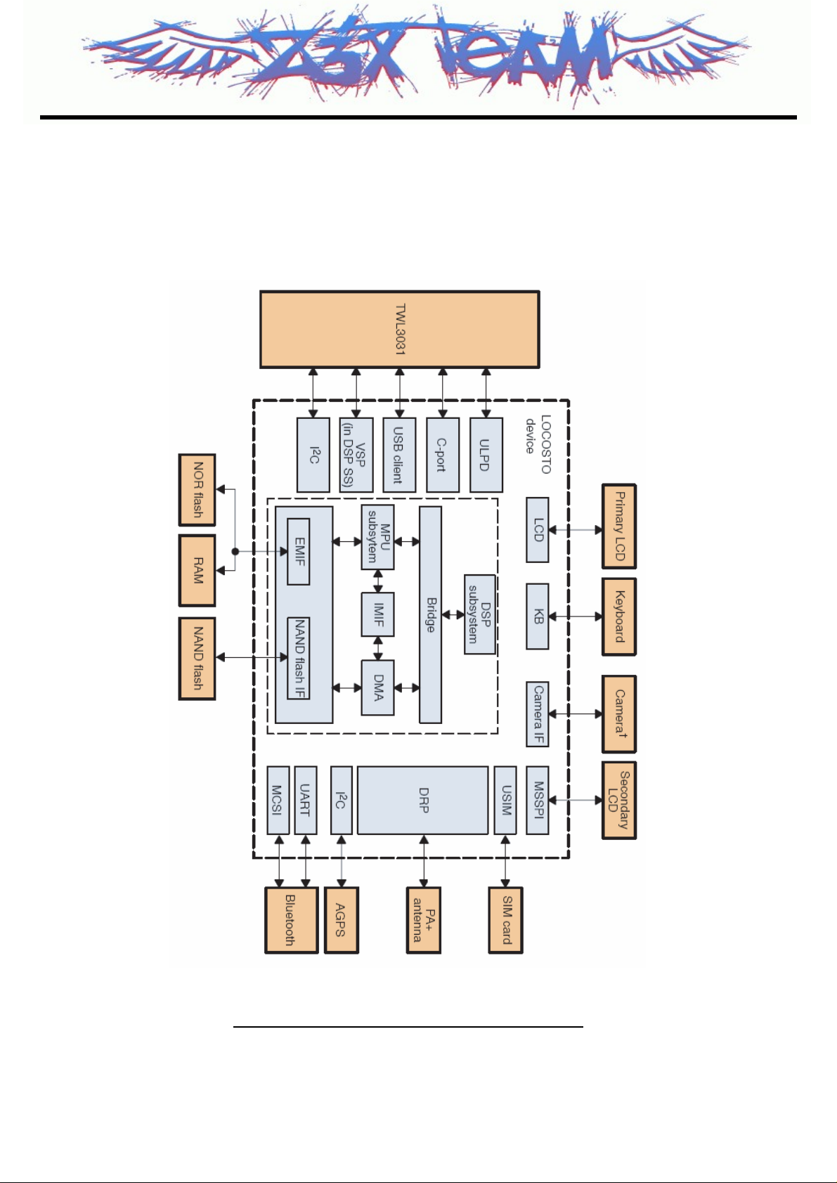
3.1 Digital Main Processor (Locosto)
Figure. 3-1 Locosto FUNCTIONAL BLOCK DIAGRAM
Z3X-BOX.COM

LGE Internal Use Only
Copyright © 2008 LG Electronics. Inc. All right reserved.
Only for training and service purposes
3. HW Circuit Description
- 17 -
3.1.1 Overview of Locosto
The Locosto is a GSM base band modem including RF transceiver covering the low bands GSM850
/GSM900 and high bands GSM1800/GSM1900 bands. Locosto is Dual Band, therefore, it supports by
default a low / high pair of bands at the same time:
1. GSM850 / GSM1800
2. GSM850 / GSM1900
3. GSM900 / GSM1800
4. GSM900 / GSM1900
The Locosto is optimized for voice-centric Mobile Phone applications.
The Locosto is designed as a single chip solution that integrates the digital, mixed-signal, RF
functionality and a direct-to-battery Power Management Unit.
The transceiver consists of:
• Constant gain direct conversion receiver with an analog I/Q base band interface
• Fully integrated Sigma/Delta-synthesizer capability
• Fully integrated two-band RF oscillator
• Two-band digital GMSK modulator with digital TX interface
• Digitally controlled crystal oscillator generating system clocks.
The Locosto supports a direct battery connection, hence eliminating the need for an external Power
Management Unit. The Locosto has different power down modes and an integrated power up
sequencer.
The Locosto is powered by the ARM7(104MHz) MCU and C54® DSP cores.
The operating temperature range from -40°C to 85°C. It is manufactured using the 0.13 µm CMOS
process.
Z3X-BOX.COM

LGE Internal Use Only
Copyright © 2008 LG Electronics. Inc. All right reserved.
Only for training and service purposes
3. HW Circuit Description
- 18 -
3.1.2 Features
The LOCOSTO device is an integrated solution that embeds a digital baseband(DBB) and a digital
radio processor (DRP) on the same die. The LOCOSTO device targets solutions for GSM/GPRS (lowcost global system for mobile communications/general packet radio service).
The DRP is a digital radio-frequency (RF) transceiver that supports up to a GPRS class12. The DRP is
designed for quad-band operation, supporting both the European and the US bands (E-GSM 900 and
DCS 1800 bands, GSM850 and PCS 1900 bands, respectively).
The DBB supports the processing of GSM radio signals in the switching circuit mode and the packet
data mode (GPRS) for up to class 10, including evolutions such as the SAIC and localization system
(A-GPS) in compliance with the European Telecommunications Standards Institute specification.
The LOCOSTO silicon process is a 90-nm digital CMOS technology.
The LOCOSTO device includes two versions: LOCOSTO and LOCOSTO Lite.
The LOCOSTO Lite device does not include the camera interface and the GPRS.
LOCOSTO offers the following features:
■ Dual processors:
- 104-MHz ARM7TDMI® microprocessor unit (MPU)
- 104-MHz customized digital signal processor (cDSP) c54x
■ Internal memory:
- 154KW DSP read-only memory (ROM)
- 30KW DSP static random-access memory (SRAM)
- 2.5Mb MPU SRAM
- 1.5Mb MPU ROM
■ External memory support:
- 1.8/3 V subscriber identity module (SIM) I/F
- Direct memory access (DMA) to external memory
- Burst mode, page-mode external memory: NAND and NOR flash and SRAM (frame buffer)
■ Hardware security
- Flash content
- International mobile equipment identity (IMEI) protection
- SIM lock
Z3X-BOX.COM

■ Peripheral interfaces
- Vibrator PWM control signal
- Universal serial bus (USB) 2.0 full-speed client
- Keypad
- Universal asynchronous receiver/transmitter (UART)
- Multichannel serial interface (MCSI)
- Bluetooth
- Camera
- Primary liquid-crystal display (LCD): 8-bit parallel interface Up to QVGA (quarter video graphics
array) 256K colors
- Secondary LCD: Serial interface
■ DRP2.0 RF integrated RF:
- Digital RF 4 band GSM/GPRS up to Class 12 (On the LOCOSTO Lite device, GSM is dual-band
muxed and GPRS is not available.)
- -110 dBm sensitivity
- Digital PA driver output level +2 dBm
- 0.7 degrees RMS phase error
- Integrated digitally controlled crystal oscillator (DCXO)
■ Software support:
- GSM/GPRS layer 1,2,3 (GPRS is not available on LOCOSTO Lite.)
- Adaptive multirate (AMR), full rate (FR), half rate (HR), enhanced full rate (EFR)
- Teletypewriter (TTY)
- SAIC over GSM
- Man machine interface (MMI) for test
- Wireless application protocol (WAP), enhanced message service(EMS), multimedia message
service (MMS), JAVA
■ Multimedia support:
- Internal 300 KP camera support
- MP3 player
- Up to 32 polyphonies stereo midi player
- Up to 32 polyphonies mono midi ringer
- JPEG encode and decode
LGE Internal Use Only
Copyright © 2008 LG Electronics. Inc. All right reserved.
Only for training and service purposes
3. HW Circuit Description
- 19 -
Z3X-BOX.COM

LGE Internal Use Only
Copyright © 2008 LG Electronics. Inc. All right reserved.
Only for training and service purposes
3. HW Circuit Description
- 20 -
The LOCOSTO device communicates with the analog TWL3031 external subsystem, which provides
the following capabilities:
- Handset microphone and speaker
- Headset mono/stereo audio speakers and microphone connection
- Melody ringer (hands-free) and buzzer
- Battery pack (Nimh/Li-ion) and six 7-V regulated or 20-V nonregulated charger
- Vibrator motor control
- Real-time clock (RTC) 32-kHz crystal
The following external/extra subsystems are also supported:
- TI-Bluetooth (BRF6150) wireless short-distance connectivity
- Voice/audio and data
- TI-AGPS/TWL5002 localization system (I/F provision)
- Digital camera systems (not available on LOCOSTO Lite)
- VGA camera sensor/module, for example, AGILENT ADCM-2700 (not available on LOCOSTO
Lite)
- OMAP-DMxx(GoldenEye) camera companion chip (up to 3M-pixel) (not available on LOCOSTO
Lite)
- UART cable or IrDA (infrared data association)
- Boot-manufacturing capability from the USB link
- FM radio receiver (for example, Philips TEA5767/68)
- Primary (Qcif) and secondary LCD
- NAND flash-based media storage (for example, on-board SmartMedia)
- USB carkit
Z3X-BOX.COM
LGE Internal Use Only
Copyright © 2008 LG Electronics. Inc. All right reserved.
Only for training and service purposes
3. HW Circuit Description
- 21 -
3.1.3 Asynchronous Operation Mode Concept
The Locosto can operate in either:
• The traditional synchronous mode with the 26MHz system clock synchronized on the base station
• A special asynchronous mode (XO concept).
In the asynchronous mode the 26MHz clock input is not synchronized with the base station; the
residual frequency offset is compensated in the digital signal processing domain. This processing
includes frequency and timing compensation of the baseband and voiceband signals.
3.1.4 Receiver Antenna Bar Display
RSSI Range (dBm)Antenna Bar
Over -92 ± 2 (dBm)
( -93 〜 -100 ) ± 2 (dBm)
skip
( -101 〜 -103) ± 2 (dBm)
( -104 〜 -105) ± 2 (dBm)
Less -106 ± 2 (dBm)
Z3X-BOX.COM
LGE Internal Use Only
Copyright © 2008 LG Electronics. Inc. All right reserved.
Only for training and service purposes
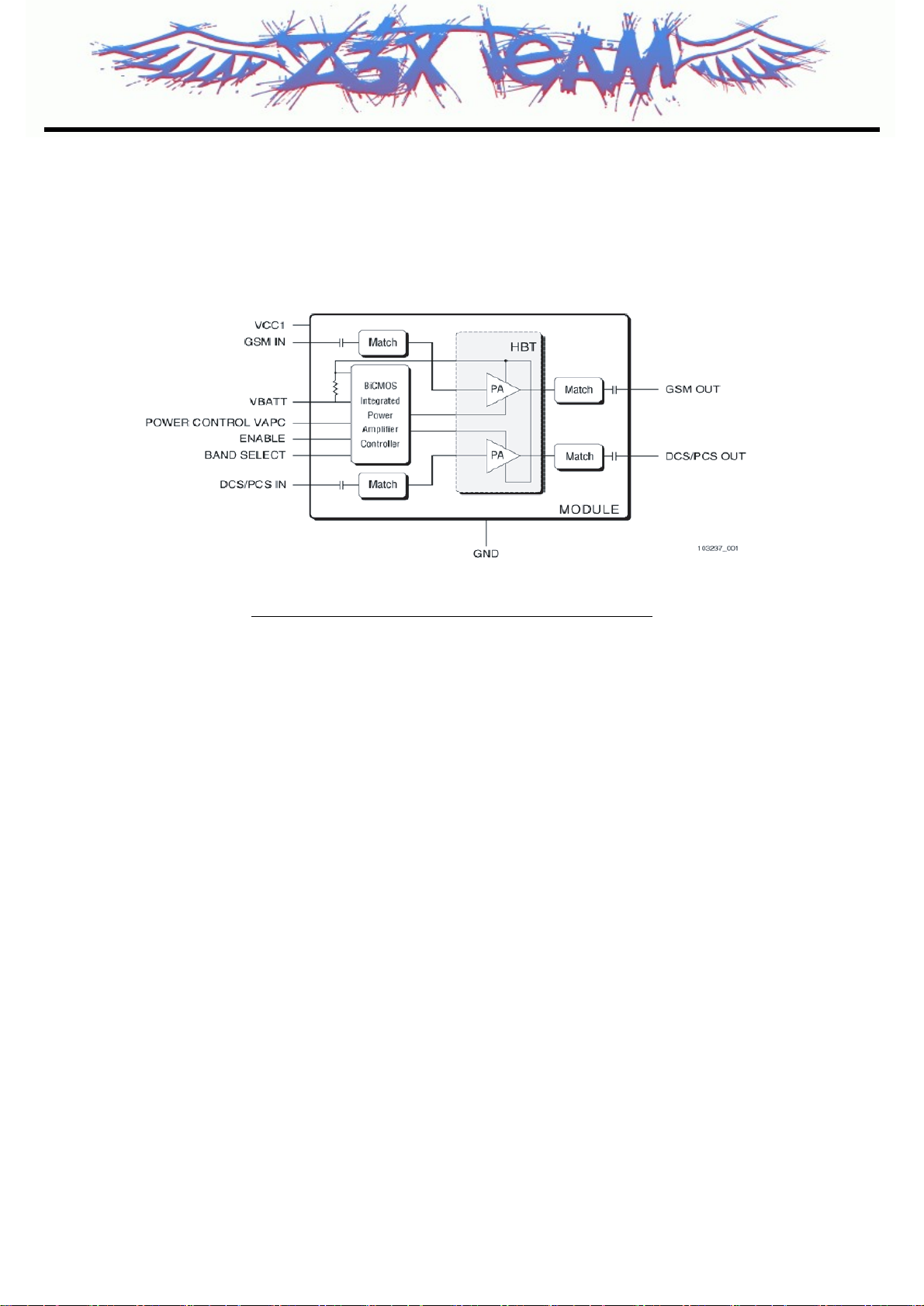
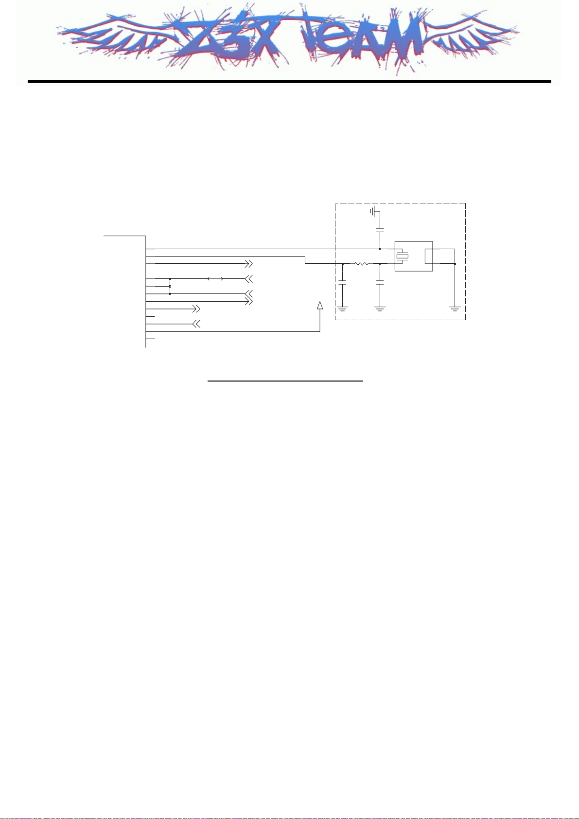
3.2 Power Amplifier Module (SKY77318)
The module consists of separate GSM PA and DCS1800/PCS1900 PA blocks, impedance-matching
circuitry for 50 Ω input and output impedances and a Power Amplifier Control (PAC) block with an
internal current-sense resistor. The custom BiCMOS integrated circuit provides the internal PAC
function and interface circuitry. Fabricated onto a single Gallium Arsenide (GaAs) die, one
Heterojunction Bipolar Transistor (HBT) PA block supports the GSM bands and the other supports the
DCS1800 and PCS1900 bands. Both PA blocks share common power supply pins to distribute
current.
The GaAs die, the Silicon (Si) die, and the passive components are mounted on a multi-layer laminate
substrate. The assembly is encapsulated with plastic overmold. RF input and output ports of the
SKY77318 are internally matched to a 50 Ω load to reduce the number of external components for a
quad-band design. Extremely low leakage current (2.5 µA, typical) of the dual PA module maximizes
handset standby time. The SKY77318 also contains band select switching circuitry to select GSM
(logic 0) or DCS/PCS (logic 1) as determined from the Band Select (BS) signal.
In Figure 1 below, the BS pin selects the PA output (DCS/PCS_OUT or GSM_OUT) and the Analog
Power Control (VAPC) controls the level of output power.
The VBATT pin connects to an internal current-sense resistor and interfaces to an integrated power
amplifier control (iPAC™) function, which is insensitive to variations in temperature, power supply,
process, and input power.
The ENABLE input allows initial turn-on of PAM circuitry to minimize battery drain. The SKY77318
Power Amplifier Module (PAM) is designed in a low profile (1.2 mm), compact form factor for quadband cellular handsets comprising GSM850/900, DCS1800, and PCS1900 operation.
The PAM also supports Class 12 General Packet Radio Service (GPRS) multi-slot operation.
3. HW Circuit Description
- 22 -
Figure. 3-2 SKY77318 FUNCTIONAL BLOCK DIAGRAM
Z3X-BOX.COM
LGE Internal Use Only
Copyright © 2008 LG Electronics. Inc. All right reserved.
Only for training and service purposes
3.3 26 MHz Clock (DCXO)
DCXO (Digitally Controlled Crystal Oscillator) and VCTCXO (Voltage Controlled Temperature
Compensated Crystal Oscillator) are two different techniques used to maintain the mobile’s reference
oscillator’s accuracy over time. The reference oscillator’s accuracy over time will vary due to initial
crystal frequency offset, temperature drift and aging. These static and dynamic frequency variations
have to be compensated, otherwise the mobile would be in danger of losing connection to the network.
The technique used to perform the frequency compensation is generally termed Automatic Frequency
Control (AFC). To summarize the operation of DCXO, GSM Baseband processor will calculate the
AFC compensation (which is continuously updated) required based on the measured frequency error.
Then the required AFC compensation is sent to the LUXO (Lineari-Zation Unit of Crystal Oscillator),
which in turns control the DCXO core and generates the 26MHz system clock.
3. HW Circuit Description
- 23 -
Figure. 3-3 Locosto DCXO Overview
C107
1000p
J12
NC10
H12
NC11
NC12
NC13
NC14
NC15
NC16
NC17
NC18
NC19
SPARE3
SPARE2
XTAL
G12
L11
K11
J11
H11
L10
K10
J10
U1
U2
D15
L8
R105
1.5M
X101
W-191-866
4
GND2
1
HOT1
26MHz
R104
220K C109
HOT2
GND1
C108
0.5p
C112
4.7p
3
2
10p
DITHERING
Z3X-BOX.COM
LGE Internal Use Only
Copyright © 2008 LG Electronics. Inc. All right reserved.
Only for training and service purposes
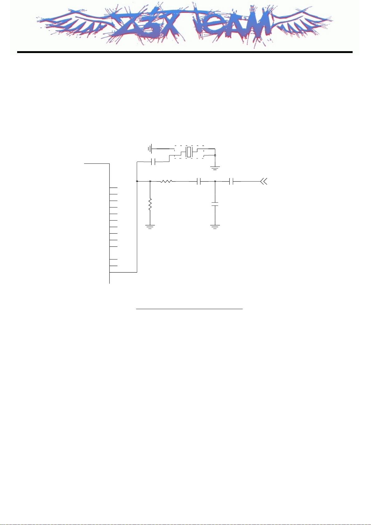
3.4 RTC(32.768KHz Crystal)
The integrated Real Time Clock (RTC) is able to provide programmable alarm functions and external
interrupts. Due to its extreme low power consumption the RTC can be supplied from a small backup
battery. This allows the generation of external interrupts, even when the main Locosto supply voltage
is switched off. For this purpose the RTC is powered by own voltage supply pins VDD_RTC and
VSS_RTC.
The RTC shall be driven by a 32.768 kHz (32k) clock which needs to be applied via the Triton(ABB)
OSC32KIN and OSC32KOUT pins. The clock can be fed from either an external clock source or use
the on chip 32 KHz oscillator module.
The low clock frequency and the optimized low power design give the possibility to run the chip with a
minimum of power dissipation. For example, for this specific application the 26 MHz reference
oscillator can be switched off during system standby and a low- power time reference can be kept
when the 32k clock is provided to the RTC.
The RTC consists of an Locosto specific RTC shell, containing the RTC macro, as well as the 32 kHz
oscillator, as described in the following sections. The module RTC Shell solely performs level
translation of the 32KHz clock to the VDD_LD1 power supply domain, and is not functionally
associated with the RTC.
3. HW Circuit Description
- 24 -
Figure. 3-4 Locosto RTC Interface
LED_A
LED_B
LED_C
VIBDR
CKEN
REGEN
HSDET
BM_SEL
R16
T16
P16
C16
E17
F17
U12
H12
G12
F16
M8
B16
CKEN
JACK_DETECT
OSC32KIN
OSC32KOUT
CLK32KOUT
BM_PRECH
CLK32K
MLED1
MLED2
MOTOR_P
V_RTC
C105
10p
R103
220K
C104
X100
15p
MC-146_7pF
4
12
C106
15p
3
32.768KHz
Z3X-BOX.COM
LGE Internal Use Only
Copyright © 2008 LG Electronics. Inc. All right reserved.
Only for training and service purposes
3.5 LCD Interface(8-bit Parallel interface)
3. HW Circuit Description
- 25 -
Signals Description
_LCD_§—MAIN_CS This signal enable to access to the driver IC of LCD.
LCD_D(0:7)_LCD_MAIN_CS This signal transfer display data to driver IC.
LCD_ADS, _LCD_WR This signal transfer control signal to driver IC.
LCD_RESET This signal makes driver IC to HW default status.
VRWLED This signal provide power to white LEDs.
MLED1/2 This signal be feed back from white LEDs.
V_EXTH, V_IO This signal provides power to LCD modules.
Figure 3-5-1. LCD Interface
V_EXTH
V_IO
CN301
54
1
53
LCD_D(0:7)
LCD_ADS
_LCD_WR
_LCD_MAIN_CS
_LCD_SUB_CS
LCD_D(7)
LCD_D(6)
LCD_D(5)
LCD_D(4)
LCD_D(3)
LCD_D(2)
LCD_D(1)
LCD_D(0)
EVRC14S03Q030100R
EVRC14S03Q030100R
LCD_ID
EAR_P
EAR_N
MOTOR_P
IND_LED_B
IND_LED_R
FL301
EVRC14S03Q030100R
FL303
FL305
R312
100K
4
3
2
1
9
8
7
6
9
8
7
6
R308
47K
SPK_P
SPK_N
INOUT_A4
INOUT_A3
INOUT_A2
INOUT_A1
INOUT_B1
INOUT_B2
INOUT_B3
INOUT_B4
INOUT_B1
INOUT_B2
INOUT_B3
INOUT_B4
G15G2
10
INOUT_B4
INOUT_B3
INOUT_B2
INOUT_B1
INOUT_A1
INOUT_A2
INOUT_A3
INOUT_A4
G110G2
INOUT_A1
INOUT_A2
INOUT_A3
INOUT_A4
G110G2
6
7
8
9
1
2
3
4
5
1
2
3
4
5
LCD_RESET
CAM_RESET
2
3
52
4
51
550
6
49
48
7
8
47
46
9
45
10
44
11
43
12
42
13
41
14
40
15
39
16
38
17
18
37
36
19
20
35
34
21
22
33
23
32
24
31
30
25
26
29
2728
C312
0.1u
VBAT
FL300
ICVE10184E050R101FR
9
8
7
6
9
8
7
6
ICVE10184E050R101FR
9
8
7
6
I2C_SDA
I2C_SCL
MLED1
MLED2
VRWLED
CAM_PWDN
C310
C311
0.1u
0.1u
C313
0.1u
INOUT_B1
INOUT_B2
INOUT_B3
INOUT_B4
INOUT_B1
INOUT_B2
INOUT_B3
INOUT_B4
INOUT_B1
INOUT_B2
INOUT_B3
INOUT_B4
1
INOUT_A1
2
INOUT_A2
3
INOUT_A3
4
INOUT_A4
G15G2
10
FL302
ICVE10184E050R101FR
1
INOUT_A1
2
INOUT_A2
3
INOUT_A3
4
INOUT_A4
G15G2
10
FL304
1
INOUT_A1
2
INOUT_A2
3
INOUT_A3
4
INOUT_A4
G110G2
5
1V8_CAM
CAM_D(7)
CAM_D(6)
CAM_D(5)
CAM_D(4)
CAM_D(3)
CAM_D(2)
CAM_D(1)
CAM_D(0)
2V8_CAM
CAM_MCLK
CAM_PCLK
CAM_HS
CAM_VS
CAM_D(0:7)
VA300
varistor
NA
VA301
VA302
VA303
1000p
C314
1u
0.1u
C316
C315
Z3X-BOX.COM
LGE Internal Use Only
Copyright © 2008 LG Electronics. Inc. All right reserved.
Only for training and service purposes
3. HW Circuit Description
- 26 -
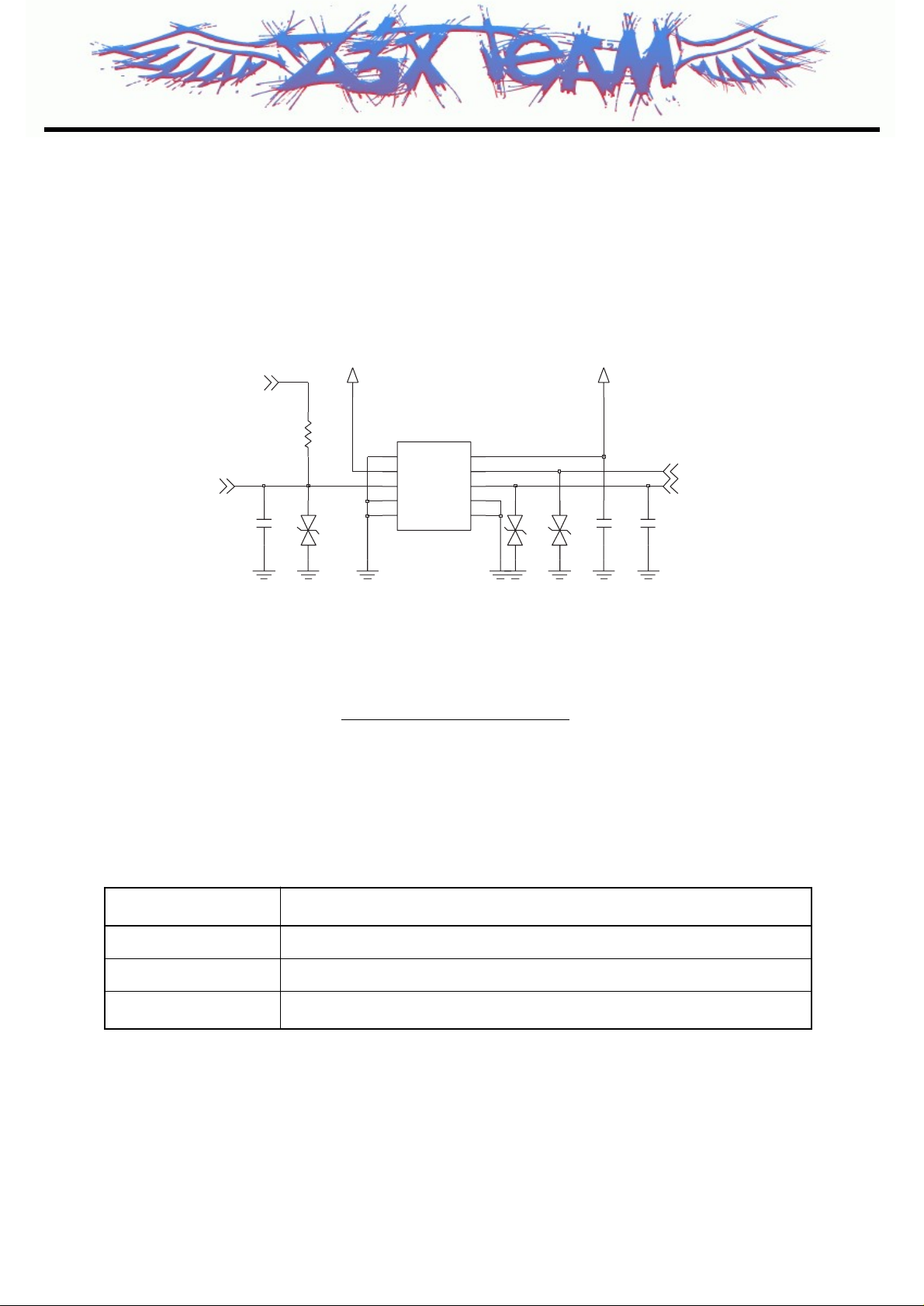
3.6 SIM Card Interface
The Locosto provides SIM Interface Module. The Locosto checks status periodically during established
call mode whether SIM card is inserted or not, but it doesn't check during deep sleep mode. In order to
communicate with SIM card, 3 signals SIM_DATA, SIM_CLK, SIM_RST.
Figure 3-6. SIM CARD Interface
Signals Description
SIM_RST This signal makes SIM card to HW default status.
SIM_CLK This signal is transferred to SIM card.
SIM_DATA This signal is interface datum.
V_SIM
SIM_PW_CTL
R130
10K
SIM_IO SIM_CLK
C145
22p
D101
DNI_DIODE_1006
4
5
6
10
9
GND1
VPP
IO
GND5
GND4
J100
VCC
RST
CLK
GND2
GND3
1
2
3
7
8
D102
V_SIM
C146
D103
0.1u
DNI_DIODE_1006
DNI_DIODE_1006
SIM_RST
C147
22p
Z3X-BOX.COM
LGE Internal Use Only
Copyright © 2008 LG Electronics. Inc. All right reserved.
Only for training and service purposes
3. HW Circuit Description
- 27 -
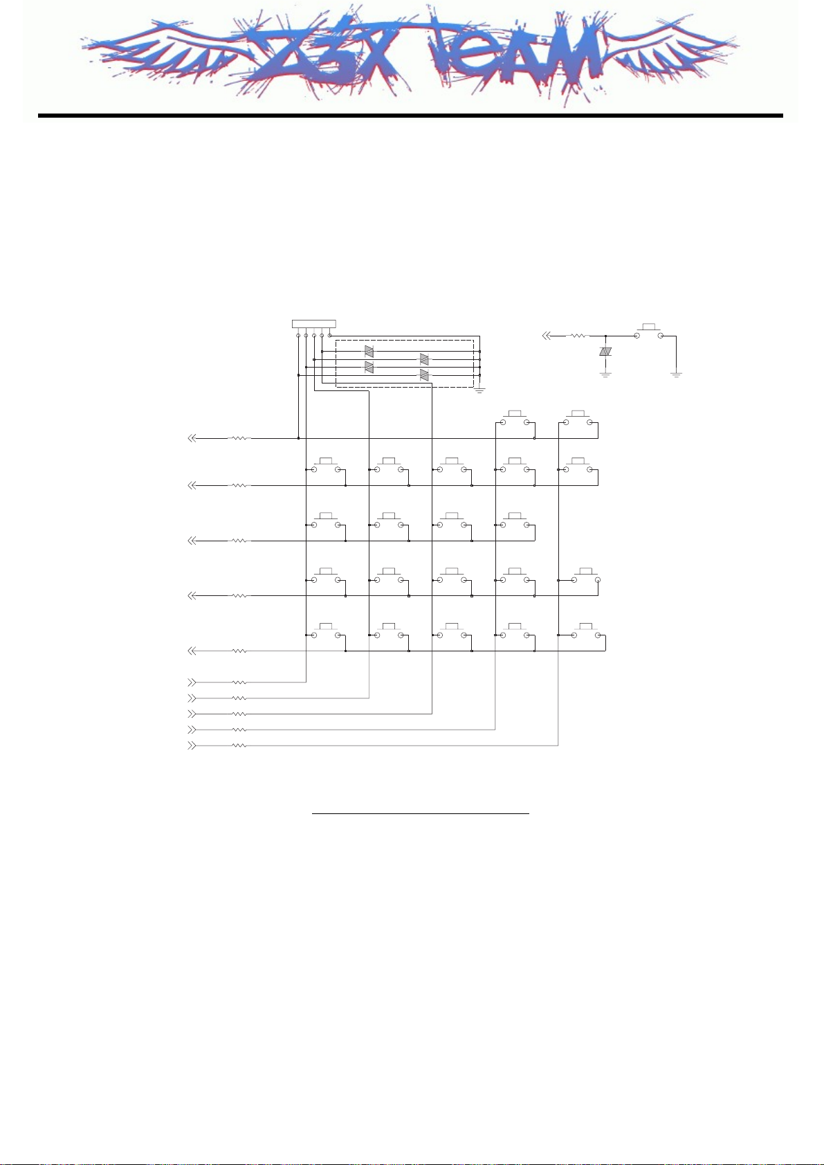
3.7 KEYPAD Interface
Figure 3-7 KEY MATRIX Interface
V_UP
V_DN
KEYPAD
CN200
12345
SPK
EVLC14S02050VA200
VA201 EVLC14S02050
EVLC14S02050VA203
VA204 EVLC14S02050
END
KB200
VA202
EVLC14S02050
RPWON
R213 150
KBR(0)
KBR(1)
KBR(2)
KBR(3)
KBR(4)
KBC(0)
KBC(1)
KBC(2)
KBC(3)
KBC(4)
R226 680
R230 680
R233 680
R235 680
R237 680
OK
OK
1
KB201
680R228
KB206
4
KB210
7
680R232
KB215
*
680R234
680R236
680R238
2
KB202 KB205
KB207
5
KB211
8
KB216
0
KB203
KB208
KB212
KB217
3
KB204
LEFT
KB209
6
9
#
KB213
KB218
UP
RIGHT
DOWN
SOFT
KB214
CLEAR
SOFT1
MENU
SEND
CLEAR
Z3X-BOX.COM

3.8 Battery Charging Block Interface
The ISL9221 is a high performance battery charger designed to charge single cell Li-Ion/Li-Poly
batteries with up to 500mA of current from an external power source. It is a stand-alone charging
solution, with just one external component required for complete functionality.
The ISL9221 precisely regulates battery charge voltage and current for 4.2V Li-Ion/Li-Poly battery
cells. The ISL9221 has four basic modes for the battery charge cycle: preconditioning/trickle charge;
constant current/fast charge; constant voltage; and end of charge.
- 28 -
3. HW Circuit Description
LGE Internal Use Only
Copyright © 2008 LG Electronics. Inc. All right reserved.
Only for training and service purposes
Figure 3-6. SIM CARD Interface
EOC
CHG_EN
DNI
R305
V_IO
R301
100K
VCHG_IN
VBUS_IN
5.6K
R303
U300 ISL9221
1
VDC
VUSB
_PPR
_CHG
_EN
IMIN
VDC_BYP
USB_BYP
2
3
4
5
6
PGND
BAT
IVDC
GND
IUSB
13
12
11
10
9
8
7
R306
33K
DNI
R307
16K
VBAT
R304
C304
VCHG VBUS
C305
0.1uF0.1uF
C306
0.1uF
Z3X-BOX.COM
3.9 RF Interface
Locosto features a fully integrated constant-gain direct conversion receiver, i.e. there is no interstage
filter needed and the baseband level at the analogue IQ- interface follows directly the RF input level.
Depending on the baseband ADC dynamic range, single- or multiple-step gain switching schemes are
possible.
An integrated, selfaligning, low-pass filter ensures the receivers to function under blocking and
reference interference conditions and avoids aliasing by baseband sampling. An automatic DC-offset
compensation is implemented and can beswitched depending on the gain setting.
- 29 -
3. HW Circuit Description
LGE Internal Use Only
Copyright © 2008 LG Electronics. Inc. All right reserved.
Only for training and service purposes
Figure 3-9-1. FEM interface
V_EXTH
ANT_SW1
ANT_SW2
C431
1000p
C432
1000p
C433
1000p
LMSP43QC-789TEMPFL400
11
19
VC1
20
VC2
21
VDD
9
GND1
10
GND2
12
GND3
13
GND4
14
GND5
16
GND6
18
GND7
22
GND8
NC2
GSM1900_RX1
ANT
GSM1900_RX2
GSM1800_RX1
GSM1800_RX2
GSM900_RX1
GSM900_RX2
GSM850_RX1
GSM850_RX2
GSM1800_1900_TX
NC1
GSM850_900_TX
23
24
1
2
3
4
5
6
7
8
15
17
Z3X-BOX.COM
- 30 -
3. HW Circuit Description
The digital transmitter architecture is based on a fractional-N sigma-delta synthesizer for constant
envelope GMSK modulation. This configuration allows a very low power design with a reduced
external component count.
The modulation is transferred between baseband- and RF-part of the PMB7880 via a digital interface
signal into the digital modulator. The following Gaussian filter shapes the digital data stream for the
GMSK modulation. Additionally a pre-distortion filter compensates the attenuation of the PLL transfer
function resulting in a very low distortion at the transmit output. The filtered digital data stream is
scaled appropriately and added to the channel word.
This sum is fed into the MASH modulator. The output of the MASH modulator is a sequence of integer
divider values representing the high resolution fractional input signal. This sequence controls the MMD
(multi modulus divider) at a sample rate of 26MHz. Thus a tightly controlled frequency modulation of
the VCO is achieved.
LGE Internal Use Only
Copyright © 2008 LG Electronics. Inc. All right reserved.
Only for training and service purposes
Figure 3-9-2. PAM (Power Amplifier Module) interface
close to DBB
0.5p
C415
3.3nH
L400
0.01u
C407
47R404
DNI
C418
ECCH0003002
C405
C2012JF1A106ZT
10u
C419
DNI
1.5p
C402
47R405
R400
15K
GND814GND9
16
21
P_GND
19
RSVD_GND
VAPC
20
17
VBATT
2
VCC1A6VCC1B
BS
1
DCS_PCS_IN
315
DCS_PCS_OUT
4
EGSM_IN
11
EGSM_OUT
ENABLE
18
GND1
5
7
GND28GND3
GND4
9
10
GND5
GND6
12
13
GND7
C400
SKY77318
U400
68p
C412
180p
C410
15p
47p
C413
C421
0.5p
27p
C423
1.5p
C422
0.5p
C403
C417
1p
1.5p
C414
L410
2.7nH
0.01u
C408
0.01u
VBAT
10nH
L404
C406
R403
10
39p
C409
VDDRF1
18nH
L403
1nH
L401
3.3nH
L411
2.2p
C401
TXLB
TXHB
TX_RAMP
PA_BAND
PA_EN
Z3X-BOX.COM
- 31 -
3. HW Circuit Description
3.10 Audio Interface
3.10.1 Uplink Path
A voice signal is converted to electrical signal with Microphone. The converted electrical voice signal is
amplified and converted to digital signal in ABB(T3031). The converted digital data is encoded to GSM
voice standard in DBB(LOCOSTO).
The audio signals from main microphone goes to MICP and MICN of ABB and the voice signal from
head-set to HSMIC of ABB. The bias voltage for microphone is 2V for main mic. and 1.8V for head-set
mic, which bias voltage is generated in ABB(MICBIAS, V_IO)
LGE Internal Use Only
Copyright © 2008 LG Electronics. Inc. All right reserved.
Only for training and service purposes
Figure 3-10-1 Main Mic interface
MICBIAS
MICIP
MICIN
R214
1K
C221
C223
DNI
L200
100nH
C220
0.1u
C222 22n
22nC224
10u
R225
DNI
C225
DNI
C217
39p
VA205
L201
100nH
0R227
MIC200
1
OUT
2
G1
3
G2
4
G3
5
PWR
6
G4
SPM0204LE5-QB
Z3X-BOX.COM
 Loading...