

Page 1
SERVICE MANUAL
SERVICE MANUAL
CAUTION
BEFORE SERVICING THE UNIT, READ THE “SAFETY PRECAUTIONS”
IN THIS MANUAL.
Internal Use Only
OCTOBER, 2016
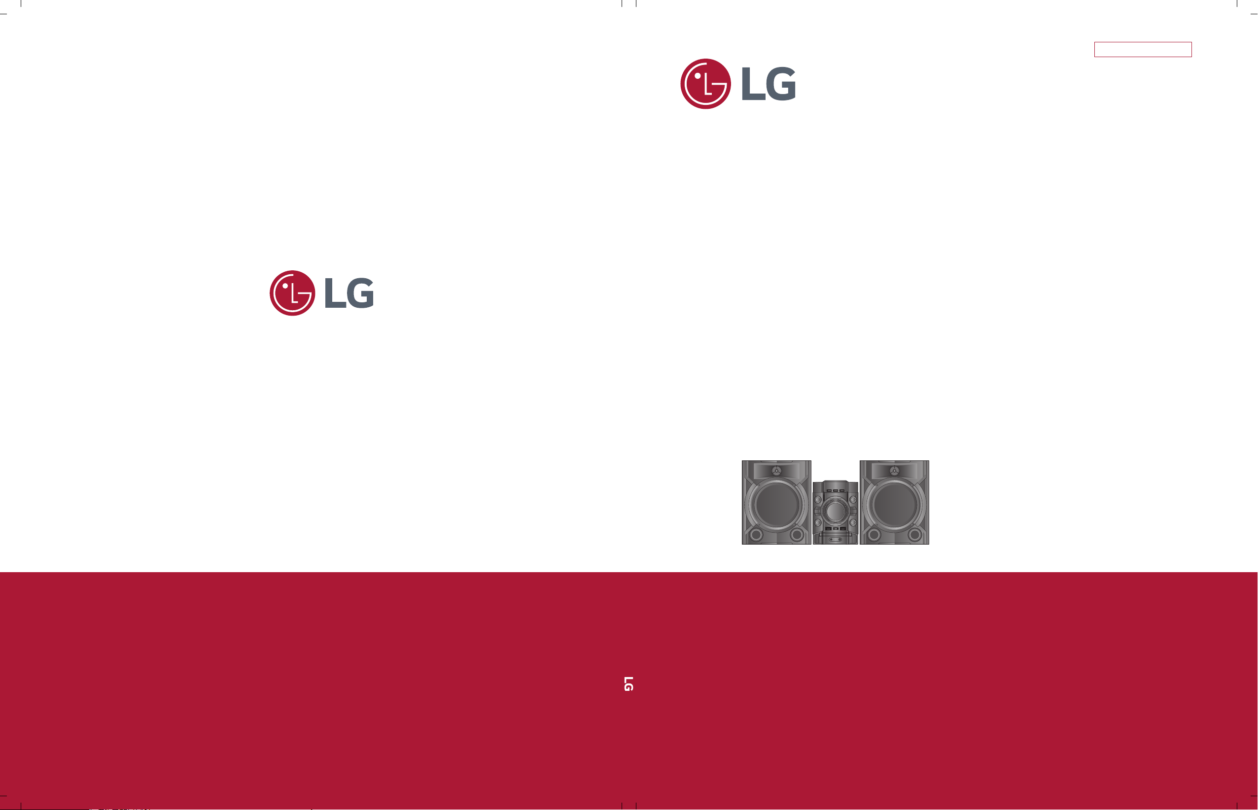
MODEL: CM5660 (CM5660, CMS5760F)
MODEL: CM5660
(CM5660, CMS5760F)
MINI HI-FI SYSTEM
P/NO : AFN77612031
Page 2

CONTENTS
SECTION 1 ........ GENERAL
SECTION 2 ........ CABINET & MAIN CHASSIS
SECTION 3 ........ ELECTRICAL
SECTION 4 ........ REPLACEMENT PARTS LIST
1-1
Page 3

SECTION 1
SUMMARY
CONTENTS
SERVICING PRECAUTIONS ............................................................................................................................ 1-3
ESD PRECAUTIONS ......................................................................................................................................... 1-5
HIDDEN KEY MODE ......................................................................................................................................... 1-6
SERVICE INFORMATION FOR EEPROM ........................................................................................................ 1-7
PROGRAM DOWNLOAD GUIDE ...................................................................................................................... 1-8
SPECIFICATIONS ........................................................................................................................................... 1-10
1-2
Page 4

SERVICING PRECAUTIONS
NOTES REGARDING HANDLING OF THE PICK-UP
1. Notes for transport and storage
1) The pick-up should always be left in its conductive bag until immediately prior to use.
2) The pick-up should never be subjected to external pressure or impact.
Storage in conductive bag
Drop impact
2. Repair notes
1) The pick-up incorporates a strong magnet, and so should never be brought close to magnetic materials.
2) The pick-up should always be handled correctly and carefully, taking care to avoid external pressure and
impact. If it is subjected to strong pressure or impact, the result may be an operational malfunction and/or
damage to the printed-circuit board.
3) Each and every pick-up is already individually adjusted to a high degree of precision, and for that reason
the adjustment point and installation screws should absolutely never be touched.
4) Laser beams may damage the eyes!
Absolutely never permit laser beams to enter the eyes!
Also NEVER switch ON the power to the laser output part (lens, etc.) of the pick-up if it is damaged.
NEVER look directly at the laser beam, and don’t allow
contact with fingers or other exposed skin.
5) Cleaning the lens surface
If there is dust on the lens surface, the dust should be cleaned away by using an air bush (such as used
for camera lens). The lens is held by a delicate spring. When cleaning the lens surface, therefore, a cotton swab should be used, taking care not to distort lens.
Pressure
Magnet
How to hold the pick-up
Cotton swab
Conductive Sheet
6) Never attempt to disassemble the pick-up.
Spring has excess pressure. If the lens is extremely dirty, apply isopropyl alcohol to the cotton swab.
(Do not use any other liquid cleaners, because they will damage the lens.) Take care not to use too much
of this alcohol on the swab, and do not allow the alcohol to get inside the pick-up.
1-3
Pressure
Page 5

NOTES REGARDING COMPACT DISC PLAYER REPAIRS
1. Preparations
1) Compact disc players incorporate a great many ICs as well as the pick-up (laser diode). These components
are sensitive to, and easily affected by, static electricity. If such static electricity is high voltage, components
can be damaged, and for that reason components should be handled with care.
2) The pick-up is composed of many optical components and other high-precision components. Care must be
taken, therefore, to avoid repair or storage where the temperature or humidity is high, where strong magnetism is present, or where there is excessive dust.
2. Notes for repair
1) Before replacing a component part, first disconnect the power supply lead wire from the unit
2) All equipment, measuring instruments and tools must be grounded.
3) The workbench should be covered with a conductive sheet and grounded.
When removing the laser pick-up from its conductive bag, do not place the pick-up on the bag. (This is
because there is the possibility of damage by static electricity.)
4) To prevent AC leakage, the metal part of the soldering iron should be grounded.
5) Workers should be grounded by an armband (1 M)
6) Care should be taken not to permit the laser pick-up to come in contact with clothing, in order to prevent
static electricity changes in the clothing to escape from the armband.
7) The laser beam from the pick-up should NEVER be directly facing the eyes or bare skin.
Armband
Resistor
(1 M)
Resistor
(1 M)
Conductive
Sheet
1-4
Page 6

ESD PRECAUTIONS
Electrostatically Sensitive Devices (ESD)
Some semiconductor (solid state) devices can be damaged easily by static electricity. Such components
commonly are called Electrostatically Sensitive Devices (ESD). Examples of typical ESD devices are integrated
circuits and some field-effect transistors and semiconductor chip components. The following techniques should
be used to help reduce the incidence of component damage caused by static electricity.
1. Immediately before handling any semiconductor component or semiconductor-equipped assembly, drain off
any electrostatic charge on your body by touching a known earth ground. Alternatively, obtain and wear a
commercially available discharging wrist strap device, which should be removed for potential shock reasons
prior to applying power to the unit under test.
2. After removing an electrical assembly equipped with ESD devices, place the assembly on a conductive surface
such as aluminum foil, to prevent electrostatic charge buildup or exposure of the assembly.
3. Use only a grounded-tip soldering iron to solder or unsolder ESD devices.
4. Use only an anti-static solder removal device. Some solder removal devices not classified as "anti-static" can
generate electrical charges sufficient to damage ESD devices.
5. Do not use freon-propelled chemicals. These can generate electrical charges sufficient to damage ESD
devices.
6. Do not remove a replacement ESD device from its protective package until immediately before you are
ready to install it. (Most replacement ESD devices are packaged with leads electrically shorted together by
conductive foam, aluminum foil or comparable conductive materials).
7. Immediately before removing the protective material from the leads of a replacement ESD device, touch the
protective material to the chassis or circuit assembly into which the device will by installed.
CAUTION : BE SURE NO POWER IS APPLIED TO THE CHASSIS OR CIRCUIT, AND OBSERVE ALL OTHER
SAFETY PRECAUTIONS.
8. Minimize bodily motions when handing unpackaged replacement ESD devices. (Otherwise harmless motion
such as the brushing together of your clothes fabric or the lifting of your foot from a carpeted floor can generate
static electricity sufficient to damage an ESD device).
CAUTION. GRAPHIC SYMBOLS
THE LIGHTNING FLASH WITH APROWHEAD SYMBOL. WITHIN AN EQUILATERAL TRIANGLE, IS
INTENDED TO ALERT THE SERVICE PERSONNEL TO THE PRESENCE OF UNINSULATED
“DANGEROUS VOLTAGE” THAT MAY BE OF SUFFICIENT MAGNITUDE TO CONSTITUTE A RISK OF
ELECTRIC SHOCK.
THE EXCLAMATION POINT WITHIN AN EQUILATERAL TRIANGLE IS INTENDED TO ALERT THE
SERVICE PERSONNEL TO THE PRESENCE OF IMPORTANT SAFETY INFORMATION IN SERVICE
LITERATURE.
1-5
Page 7
HIDDEN KEY MODE
HIDDEN MODE ENTRANCE KEY EXIT KEY
Version Check
EEPROM Initial
Option EDIT
APD Test Display Front ‘Stop’ + Remote Control Key ‘3’ for 5 s Auto Exit
Clip Front ‘Stop’ + Remote Control Key ‘Mute’ for 5 s Auto Exit
Disc Lock
On/ Off
Power Disc Lock
On/ Off
Demo All Key Lock Front ‘Stop’ + Remote Control Key ‘9’ for 5 s Front ‘Stop’ + Remote Control Key ‘9’ for 5 s
Bluetooth Auto Power
On/ Off
Child Safe
On/ Off
Front ‘Stop’ + Remote Control Key ‘ ’ for 5 s Remote Control Key ‘ ’ for 1.5 s
Front ‘Stop’ + Remote Control Key ‘
Front ‘Stop’ + Remote Control Key ‘
Front ‘Stop’ + Remote Control Key ‘Stop’ for 5 s Front ‘Stop’ + Remote Control Key ‘Stop’ for 5 s
Front ‘Stop’ + Remote Control Key ‘Region EQ’ for 5 s
or
Front ‘Stop’ + Front ‘Open’ for 5 s
Front/ Remote Control Key ‘Power’ for 5 s
Volume 0 (Min) + Front ‘Enter’ for 3 s Volume 0 (Min) + Front ‘Enter’ for 3 s
/ /
’ for 5 s
Auto Exit
’ for 5 s Front ‘Stop’ + Remote Control Key ‘ ’
Front ‘Stop’ + Remote Control Key ‘Region EQ’ for 5 s
Front ‘Stop’ + Front ‘Open’ for 5 s
Front/ Remote Control Key ‘Power’ to SET ‘Power Off’
or
1-6
Page 8

SERVICE INFORMATION FOR EEPROM
POWER ON
VFD “NO DISC” status
It is possible at any function.
(ex. It is possible at VFD “NO USB” status, too.)
This is an example.
Front ‘Stop’ + Remote control ‘ ’
push same timing during 5 s
FLD “OP00-…..”
Move to appropriate position
And make changes with remote control
“ , , , REPEAT” key.
/
Press ‘Stop’ Key
VFD “WRITE OK”
DETECT NEW EEPROM
(OPTION EDIT SCREEN)
NAME
OPT0
OPT1
OPT2
OPT3
OPT4
OPT5
OPT6
OPT7
OPT8
OPT9
OPT10
OPT11
OPT12
OPT13
OPT14
HEX
00
00
00
00
00
00
00
00
00
00
00
00
00
00
00
Front ‘Stop’ + Remote control ‘ ’
push same timing during 5 s
VFD “E2P CLR”
Completed
1-7
Page 9
PROGRAM DOWNLOAD GUIDE
1. DSP PROGRAM
Download program file name must be HG640_CM5760(CM5660)_YYMMDDX.bin
If security program(Water Wall) is activated on PC, you must save the file to the USB storage device
and disable the security software, then download the file to your set.
Downloading file proceeds in the same way at USB1 function and USB2 function.
Caution:
When downloading the file, you should neither unplug the USB device, change to the other function,
nor power off the device. USB device must be unplugged when the downloading process is completed.
ON VFD DISPLAY SCREEN
NO USB
Insert USB device at USB function.
SEARCH
FIRMWARE
FINISH
AUTO POWER OFF
1) (Fast) Format USB device.
2) Copy Firmware file to USB device.
1-8
Page 10

2. EQ PROGRAM
Download program file name must be EQ_PRG.BIN
If security program(Water Wall) is activated on PC, you must save the file to the USB storage device
and disable the security software, then download the file to your set.
Downloading file proceeds in the same way at USB1 function and USB2 function.
Caution:
When downloading the file, you should neither unplug the USB device, change to the other function,
nor power off the device. USB device must be unplugged when the downloading process is completed.
ON VFD DISPLAY SCREEN
NO USB
Insert USB device at USB function.
SEARCH
EQ UP
FINISH
AUTO POWER OFF
1) (Fast) Format USB device.
2) Copy Firmware file to USB device.
1-9
Page 11

SPECIFICATIONS
• GENERAL
Power requirements Refer to the main label on the unit.
Power consumption Refer to the main label on the unit.
Networked standby : 0.5 W (If all network ports are activated.)
Dimensions (W x H x D) Approx. 207 mm x 282 mm x 261 mm
Net Weight Approx. 3.5 kg
Operating temperature 5 °C to 35 °C
Operating humidity 5 % to 90 %
• INPUTS
Analog audio in (AUX IN) 2.5 Vrms (1 kHz, 0 dB), 75 Ω, RCA jack (L, R)
Portable in (PORT. IN) 1.4 Vrms (3.5 mm stereo jack) x 1
Microphone (MIC) Sensitivity 20 mV (1 kHz), 6.3 mm jack x 1
• TUNER
FM Tuning Range 87.5 to 108.0 MHz or 87.50 to 108.00 MHz
AM Tuning Range 522 to 1,620 kHz, 520 to 1,710 kHz or 522 to 1,710 kHz
• SYSTEM
Frequency Response 70 to 20,000 Hz
Signal-to-noise ratio More than 75 dB
Dynamic range More than 75 dB
Bus Power Supply (USB) 5 V 500 mA
• AMPLIFIER (RMS OUTPUT POWER)
Total 700 W
Front 350 W x 2 (4 Ω at 1 kHz, 20 % THD)
• FRONT SPEAKER
Type 2 Way 2 Speaker
Impedance 4 Ω
Rated Input Power 350 W
Max. Input power 700 W
Net Dimensions (W x H x D) Approx. 299 mm x 363 mm x 230 mm
Net Weight Approx. 5 kg
• Design and specifications are subject to change without notice.
1-10
Page 12

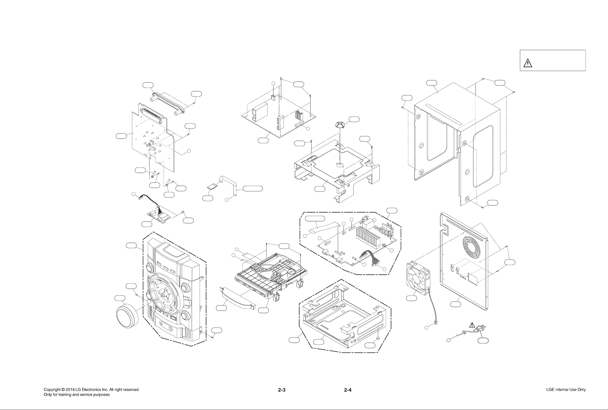
SECTION 2
CABINET & MAIN CHASSIS
CONTENTS
EXPLODED VIEWS ......................................................................................................................................... 2-3
1. CABINET AND MAIN FRAME SECTION ................................................................................................. 2-3
2. PACKING ACCESSORY SECTION ......................................................................................................... 2-7
3. SPEAKER SECTION ................................................................................................................................ 2-8
2-1
Page 13

2-2
Page 14
FRONT
MAIN
SMPS
300300
B/T
E
C
D
H
D
G
G
F
C
B
A
H
F
E
A52
A42
443
443
259
443
A47
443
264
443
263
A46
265
A44
266
269
262
443
443
260
443
443
251
443
443
443
255
255
443
254
A43
A56
498
CABLE1
CABLE4
A
B
443
A00
300300
H
EXPLODED VIEWS
1. CABINET AND MAIN FRAME SECTION
NOTES) THE EXCLAMATION POINT WITHIN AN
EQUILATERAL TRIANGLE IS INTENDED
TO ALERT THE SERVICE PERSONNEL
TO THE PRESENCE OF IMPORTANT
SAFETY INFORMATION IN SERVICE
LITERATURE.
Page 15
Page 16

2. PACKING ACCESSORY SECTION
801 Owner’s manual
825 FM Wire Antenna
804 Bag
808 Battery
900 Remote Control
803 Packing
803 Packing
802 Box
2-7
Page 17

3. SPEAKER SECTION
A60
2-8
Page 18

SECTION 3
ELECTRICAL
CONTENTS
ONE POINT REPAIR GUIDE ............................................................................................................................ 3-2
1. NO POWER ............................................................................................................................................ 3-2
2. NO BOOTING WHEN POWER ON THE SET........................................................................................ 3-4
3. VFD IS NOT DISPLAYED WHEN POWER ON THE SET ..................................................................... 3-5
4. NO BOOTING (IN CD/USB FUNCTION) ................................................................................................ 3-6
5. NO OPERATION OF MD ........................................................................................................................ 3-9
6. NO SOUND ........................................................................................................................................... 3-14
ELECTRICAL TROUBLESHOOTING GUIDE ................................................................................................. 3-22
1. POWER (SMPS) ................................................................................................................................... 3-22
2. MCS PART CHECK .............................................................................................................................. 3-25
3. FLD DISPLAY CHECK ......................................................................................................................... 3-26
4. PWM MODULATION CHECK ............................................................................................................... 3-27
5. POWER AMP PART CHECK ............................................................................................................... 3-28
6. TUNER / AUX FUNCTION CHECK ...................................................................................................... 3-29
7. TUNER FUNCTION CHECK................................................................................................................. 3-30
8. CD FUNCTION CHECK ........................................................................................................................ 3-31
9. DOUBLE USB FUNCTION ................................................................................................................... 3-32
WAVEFORMS OF MAJOR CHECK POINT .................................................................................................... 3-33
1. DSP (IC500) .......................................................................................................................................... 3-33
2. SDRAM (IC504) .................................................................................................................................... 3-34
3. SERVO (IC401) ..................................................................................................................................... 3-35
4. MOTOR DRIVER (IC400) ..................................................................................................................... 3-36
5. ADC (IC202) .......................................................................................................................................... 3-37
6. USB (JK500) ......................................................................................................................................... 3-37
7. BLUETOOTH (CN501) .......................................................................................................................... 3-38
WIRING DIAGRAM .......................................................................................................................................... 3-39
BLOCK DIAGRAMS ........................................................................................................................................ 3-41
1. SYSTEM BLOCK DIAGRAM ................................................................................................................ 3-41
2. POWER BLOCK DIAGRAM ................................................................................................................. 3-43
CIRCUIT DIAGRAMS ...................................................................................................................................... 3-45
1. SMPS CIRCUIT DIAGRAM .................................................................................................................. 3-46
2. MAIN - DSP SoC CIRCUIT DIAGRAM ................................................................................................. 3-47
3. MAIN - POWER PART CIRCUIT DIAGRAM ........................................................................................ 3-49
4. MAIN - ADC/DAC CIRCUIT DIAGRAM ................................................................................................ 3-51
5. MAIN - RF SERVO CIRCUIT DIAGRAM .............................................................................................. 3-53
6. MAIN - PWM/AMP IC CIRCUIT DIAGRAM .......................................................................................... 3-55
7. FRONT CIRCUIT DIAGRAM ................................................................................................................ 3-57
8. JACK CIRCUIT DIAGRAM ................................................................................................................... 3-59
CIRCUIT VOLTAGE CHART ........................................................................................................................... 3-61
1. ICs VOLTAGE ....................................................................................................................................... 3-61
2. CAPACITORS VOLTAGE ..................................................................................................................... 3-62
PRINTED CIRCUIT BOARD DIAGRAMS ....................................................................................................... 3-63
1. SMPS P.C.BOARD ............................................................................................................................... 3-63
2. MAIN P.C.BOARD ................................................................................................................................ 3-65
3. FRONT P.C.BOARD ............................................................................................................................. 3-67
4. JACK P.C.BOARD ................................................................................................................................ 3-69
3-1
Page 19

ONE POINT REPAIR GUIDE
1. NO POWER
If the unit doesn’t work by no power problem, repair the set according to the following guide.
1-1. FUSE/ THERMISTOR/ BRIDGE DIODE
1-1-1. Solution
Please check and replace F901, TH901 or TH903, BD901 on SMPS board.
1-1-2. How to troubleshoot (Countermeasure)
1) Check if the fuse F901 is open or short-circuit.
2) Check if the NTC thermistor TH900 or TH903 is normal or open.
3) Check if the bridge diode BD901 is short-circuit by over current with a digital multi-meter.
1-1-3. Service hint (Any picture/ Remark)
< F901 >
If F901 is not short-circuit,
replace it with a same
specifi cations one.
<TH901 or TH903 >
If TH901 or TH903 is open,
replace it with a new one.
3-2
< BD901 >
If BD901 is short-circuit,
replace it with a new one.
Page 20

ONE POINT REPAIR GUIDE
1. NO POWER
If the unit doesn’t work by no PVDD problem, repair the set according to the following guide.
1-2. FUSE/ FET
1-2-1. Solution
Please check and replace F901, Q901 on SMPS board.
1-2-2. How to troubleshoot (Countermeasure)
1) Check if the fuse F901 is open or short-circuit.
2) Check the anode-cathod voltage of D951 with a digital multi-meter, it is normally 0.2 ~ 0.3 V.
If it doesn’t have any voltage, it’s destroyed. Replace it with a new one.
1-2-3. Service hint (Any picture/ Remark)
< SMPS circuit >
3-3
Page 21

ONE POINT REPAIR GUIDE
X500
(24 MHz)
X501
(32.768 kHz)
KEY1
(R518)
PWR_CTRL
(R577)
IC500
2. NO BOOTING WHEN POWER ON THE SET
The set doesn’t work when press the power button on the top board or the remote control.
2-1. IC500
2-1-1. Solution
Please check and replace IC500 on MAIN board.
2-1-2. How to troubleshoot (Countermeasure)
1) Check the +12 VA (CN102) and 3.3 VA (IC501) in standby mode.
If there is no 12 VA, check the SMPS and if doesn’t appear 3.3 VA, check IC501.
2) Check +12 VA, +5.1 VA, 3.3 VA, DVCC_5V and DVCC_3.3V when power on the set.
If the set doesn’t work regardless of what the KEY1 changes high to low while pressing the power button.
-
X500 and X501 work normally but, if you can not power on the set, replace the IC500 with a new one
on the MAIN board.
2-1-3. Service hint (Any picture/ Remark)
KEY1
(R518)
PWR_CTRL
(R577)
X500
(24 MHz)
IC500
X501
(32.768 kHz)
< MAIN board top view >
3-4
Page 22

ONE POINT REPAIR GUIDE
3. VFD IS NOT DISPLAYED WHEN POWER ON THE SET
When power on the set, any icons or characters on VFD are not displayed.
3-1. VFD (VFD300)
3-1-1. Solution
Please check and replace VFD300 on FRONT board.
3-1-2. How to troubleshoot (Countermeasure)
1) Check if VFD_12V, DVCC_3.3V and VCC_5V are output from SMPS to VFD via the MAIN board.
2) Check if the IC501 outputs VFD_CLK, VFD_STB, and VFD_DAT to the FRONT board.
3) Check if the VFD grid current amplifier circuit on the FRONT board.
Check the drive signal to the transistor’s(Q801, Q802) base.
If the control signals from VFD (DGND, VDD) isn’t output, replace VFD with a new one.
3-1-3. Service hint (Any picture/ Remark)
< FRONT circuit >
R307(TP302)
Q300 Emitter
< Waveform of the grid current driver>
about
30 Vp-p
3-5
Page 23

ONE POINT REPAIR GUIDE
IC103
IC100
IC102
4. NO BOOTING (IN CD/USB FUNCTION)
After you turn on power key and displayed message in the following order (HELLO VOL XX
CD or USB) on VFD, it will not display other message on VFD, and it will not boot-up normally.
4-1. NO DVCC_3.3V, 1.2 VA
4-1-1. Solution
Please check and replace IC100, IC102 on MAIN board.
4-1-2. How to troubleshoot (Countermeasure)
1) Check voltage of IC102 pin3 on MAIN board.
If IC102 pin3 (about 5.1 V) & pin1 Input 12 VA doesn’t come out, check +12 VA from SMPS board.
2) If IC102 pin3 (about 5.1 V) is normal, check voltage of IC100 pin3 (about 1.2 VA), pin6 (about 3.3 VA).
If IC100 pin3 (about 1.2 VA), pin6 (about 3.3 VA) doesn’t come out, check R100, R101, R102 and R112, R113, R114.
If there’s no defective component then replace IC100.
3) PWR_CTRL is high, check R116 and if there’s no defective component then replace IC103.
PWR_CTRL (IC103 pin3) is high (about 3.2 V)
If PWR_CTRL isn’t high, check pin D11 of IC500 & R116, R117.
4) If PWR_CTRL is high, check R577 and if there’s no defective component then replace IC103.
4-1-3. Service hint (Any picture/ Remark)
IC103
IC100
IC102
< MAIN board top view >
3-6
Page 24

ONE POINT REPAIR GUIDE
XI
XO
X500
IC500
4. NO BOOTING (IN CD/USB FUNCTION)
After you turn on power key and displayed message in the following order (HELLO VOL XX
CD or USB) on VFD, it will not display other message on VFD, and it will not boot-up normally.
4-2. CRYSTAL (X500)
4-2-1. Solution
Replace X500 on MAIN board.
4-2-2. How to troubleshoot (Countermeasure)
1) If 3.3 VA & 1.2 VA is normal, check reset ‘High’ of IC500 pin T12 on MAIN board.
2) If MAIN_RESET is high, check the soldering status of 24 MHz crystal (X500).
3) If the crystal (X500) doesn’t oscillate, check R574, C544, C547 around crystal (X500).
If there’s no defective component, then replace X500.
4-2-3. Service hint (Any picture/ Remark)
X500
IC500
< MAIN board top view >
X
X500
< Signal waveform >
3-7
Page 25

ONE POINT REPAIR GUIDE
VCC
CLK
DO
CS#
IC501
4. NO BOOTING (IN CD/USB FUNCTION)
After you turn on power key and displayed message in the following order (HELLO VOL XX
CD or USB) on VFD, it will not display other message on VFD, and it will not boot-up normally.
4-3. SERIAL FLASH (IC501)
4-3-1. Solution
Please check and replace IC501 on MAIN board.
4-3-2. How to troubleshoot (Countermeasure)
1) If the crystal (X500) does oscillate, check serial flash (IC501) on MAIN board.
Check pin8 (VCC), pin6 (CLK), pin1 (CS), pin2 (DO), pin5 (DI) of below waveform.
2) If pin1, 2, 5, 6 doesn’t come out, check registers (R595, R596, R570, R571, R572, R569) of IC501.
If registers of IC500 is OK, then replace IC500. (it need to download program.)
3) After change IC500, if It is still not below waveform, check IC500 (DSP IC).
4-3-3. Service hint (Any picture/ Remark)
V
IC501
< MAIN board top view >
< Signal waveform >
3-8
Page 26

ONE POINT REPAIR GUIDE
SPIN+ (TP421)
SPIN- (TP423)
5. NO OPERATION OF MD
When no sound output in the CD function, you can not listen to music reading data from a CD
disc if the servo motors in MD don’t work. This step is for checking the SPINDLE moter among
them.
5-1. SPINDLE MOTOR
5-1-1. Solution
Please check and replace IC400 on MAIN board.
5-1-2. How to troubleshoot (Countermeasure)
1) Check the SPDO signal from pin16 of IC401.
If no signal, check DVCC_3.3V and DV 3.3 V (RF) and X400.
2) Check the SPIN+ & SPIN- from IC400 to CN401 for driving SPINDLE motor. It is about 3.6 Vp-p.
If no signal, check M_5 V for IC400.
3) Check if the FFC cable is solidly connected between CN401 and MD.
4) Check the MD.
If the spindle motor is sort-circuit or has any trouble, it can not rotate CD discs.
Please check the function after changing another MD.
5-1-3. Service hint (Any picture/ Remark)
< Waveform of SP- & SP+
for driving SPINDLE motor >
SPIN+ (TP421)
SPIN- (TP423)
< MAIN board bottom view >
3-9
Page 27

ONE POINT REPAIR GUIDE
SLED+ (TP422)
SLED- (TP424)
5. NO OPERATION OF MD
When no sound output in the CD function, you can not listen to music reading data from a CD disc
if the servo motors in MD don’t work. This step is for checking the SLED MOTOR among them.
5-2. SLED MOTOR
5-2-1. Solution
Please check and replace IC400 on MAIN board.
5-2-2. How to troubleshoot (Countermeasure)
1) Check the SLDO signal from pin15 of IC401.
If no signal, check DVCC_3.3V and DV_3.3V (RF) and X400.
2) Check the SPED+ & SLED- from IC400 to CN401 for driving SPINDLE motor. It is about 2.9 Vp-p.
If no signal, check M_5V for IC400.
3) Check if the FFC cable is solidly connected between CN401 and MD.
4) Check the MD.
If the SPINDLE motor is sort-circuit or has any trouble, it can not rotate CD discs.
Please check the function after changing another MD.
5-2-3. Service hint (Any picture/ Remark)
SP+
SP-
< Waveform of SLED- & SLED+
for driving SLED motor >
SLED+ (TP422)
SLED- (TP424)
< MAIN board bottom view >
3-10
Page 28

ONE POINT REPAIR GUIDE
MOT_CLOSE: pin6
MOT_OPEN: pin7
LOAD+: pin9
LOAD-: pin10
IC400
5. NO OPERATION OF MD
When no sound output in the CD function, you can not listen to music reading data from a CD
disc if the servo motors in MD don’t work. This step is for checking the TRAY OPEN/CLOSE
MOTOR among them.
5-3. TRAY OPEN/CLOSE MOTOR
5-3-1. Solution
Please check and replace IC400 on MAIN board.
5-3-2. How to troubleshoot (Countermeasure)
1) Check MOT_OPEN & MOT_CLOSE signals from pin P5, L4 of IC500 to IC400.
If no signal, check M_5V to IC400.
2) Check LOAD± from IC400 to CN401 for driving the tray OPEN/CLOSE motor. It is about 3.85 Vp-p.
If no signal, check M_5V to IC400. If it has any trouble, replace it with a new one.
3) Check if the FFC cable is solidly connected between CN401 and MD.
4) Check the MD.
If the tray motor is sort-circuit or has any trouble, it can not open or close the tray.
Please check the function after changing another MD.
5-3-3. Service hint (Any picture/ Remark)
LO-
LO+(RED)
MOT_OP EN
MOT_ CL OSE
< Waveform
for driving tray open/ close motor >
LOAD+: pin9
LOAD-: pin10
< MAIN board top view >
MOT_CLOSE: pin6
MOT_OPEN: pin7
IC400
3-11
Page 29

ONE POINT REPAIR GUIDE
TR+: pin15
TR-: pin16
IC400
5. NO OPERATION OF MD
When no sound output in the CD function, you can not listen to music reading data from a CD
disc if the pickup module in MD doesn’t work. This step is for checking the LASER TRACKING
ACTUATOR.
5-4. LASER TRACKING ACTUATOR
5-4-1. Solution
Please check and replace IC400 on MAIN board.
5-4-2. How to troubleshoot (Countermeasure)
The tracking actuator makes the laser beam be positioned in the center of a track on CD disc.
1) Check the TRD signal from pin14 of IC401.
If no signal, check DVCC_3.3V & DV_3.3V (RF) and X400.
2) Check TR- & TR+ from IC400 to CN400 for driving the tracking actuator.
If no signal, check M_5V for IC400.
3) Check if the FFC cable is solidly connected between CN400 and MD.
4) Check the MD.
If the pickup module has any trouble, it can not move the laser beam on the left or right side.
Please check the function after changing another MD.
5-4-3. Service hint (Any picture/ Remark)
< Waveform of TR±
for driving tracking actuator >
IC400
TR+: pin15
TR-: pin16
< MAIN board top view >
3-12
Page 30

ONE POINT REPAIR GUIDE
F-: pin13
F+: pin14
IC400
5. NO OPERATION OF MD
When no sound output in the CD function, you can not listen to music reading data from a CD
disc if the pickup module in MD doesn’t work. This step is for checking the LASER FOCUSING
ACTUATOR.
5-5. LASER FOCUSING ACTUATOR
5-5-1. Solution
Please check and replace IC400 on MAIN board.
5-5-2. How to troubleshoot (Countermeasure)
The focusing actuator makes the laser beam keep a regular interval with the surface of a CD disc.
1) Check the FDO signal from pin13 of IC401.
If no signal, check DVCC_3.3 & DV_3.3V(RF) and X400.
2) Check F- & F+ from IC400 to CN400 for driving the focusing actuator.
If no signal, check M_5V for IC400.
3) Check if the FFC cable is solidly connected between CN400 and MD.
4) Check the MD.
If the pickup module has any trouble, it can not move the laser beam on the top or bottom side.
Please check the function after changing another MD.
5-5-3. Service hint (Any picture/ Remark)
< Waveform of F±
for driving focusing actuator >
F-: pin13
F+: pin14
< MAIN board top view >
IC400
3-13
Page 31

ONE POINT REPAIR GUIDE
IC500
6. NO SOUND
There is no sound output in the CD function, repair the set according to the following guide.
6-1. CD FUNCTION
6-1-1. Solution
Please check and replace IC500 on MAIN board.
6-1-2. How to troubleshoot (Countermeasure)
1) Check CD_BCK, CD_LRCK, & CD_DATA signals from IC500 to IC401.
If no signal, check if the RF & servo signals from MD is entered to IC401.
Refer to the “No operation of MD” guide on Item 5.
2) Check the following I2S signal flow. < I2S audio signal Interface >
- MCS_BCK : IC500_pin E1 --> IC700_pin23
- MCS_LRCK : IC500_pin D1 --> IC700_pin22 (44.1 kHz)
- MIX_DATA0_OUT : IC500_pin E2 --> IC700_pin24
- MCS_MCLK : IC500_pin D2 --> IC102_pin44
If there is any trouble, check the power for each IC.
The power is normal but, if the signal waveform to the IC is distorted or no signal,
replace it with a new one.
6-1-3. Service hint (Any picture/ Remark)
< MAIN - DSP circuit >
< Waveform of I2S audio interface signals >
3-14
IC500
< MAIN board top view >
Page 32

ONE POINT REPAIR GUIDE
IC702
L703
L701
L702
L704
IC701
IC700
6. NO SOUND
There is no sound output by DIGITAL AUDIO AMP DAMAGE, repair the set according to the
following guide.
6-2. DIGITAL AUDIO AMP DAMAGE
6-2-1. Solution
Please check and replace IC701, IC702 on MAIN board.
6-2-2. How to troubleshoot (Countermeasure)
1) Check PWM_FL±, PWM_FR± & PWM_SW± signals from IC601 to IC701 & 702 each input function.
If no signal, check if I2S audio signals are entered to IC601.
Refer to “I2S audio signal interface” on Item 6-1-2.
2) Check PVDD.
If PVDD is abnormal, check the SMPS.
3) Check AMP_12V for driving the gate of AMP IC.
a. All the powers are normal, but if AMP_12V is low, there is possible for AMP IC to be damaged.
b. Remove L701, L702, L703 and L704 one by one.
When removed a inductance, if AMP_12V is recovered, the IC connected to it was damaged.
c. Replace the IC with a new one.
4) Check the impedance between IC701/ IC702_OUT_A/OUT_B & GND.
a. If the impedance is 0 Ω, the IC must be damaged.
b. After removing the heat sink, replace it with a new one.
6-2-3. Service hint (Any picture/ Remark)
IC702
L703
L702
L704
IC700
IC701
L701
< MAIN board top view >
3-15
Page 33

ONE POINT REPAIR GUIDE
D+
D-
JK500
(USB2.0)
JK501
(USB1.1)
6. NO SOUND
There is no sound output in the USB function, repair the set according to the following guide.
6-3. USB FUNCTION
6-3-1. Solution
Please check and replace IC104 on MAIN board.
6-3-2. How to troubleshoot (Countermeasure)
1) Check +5V_USB to USB board.
If the USB LED are turned on, the voltage is okay, if so not, check USB_5V voltage (pin6 of IC104).
2) Check USB D1± or USB D2± from MAIN board to top board.
a. Check 2.0_D1±signals(pin2, pin3 of JK500) or 1.1_D1± signals(pin2, pin3 of JK501) to IC500.
b. If there is any trouble, check the power for IC104.
The power is normal but, if the signal waveform to the IC is distorted or no signal, replace it with a new one.
6-3-3. Service hint (Any picture/ Remark)
D
USB D-/D+ (JK500 pin2, pin3)
< Waveform of USB D± signal >
JK500
(USB2.0)
< MAIN board top view >
JK501
(USB1.1)
3-16
Page 34

ONE POINT REPAIR GUIDE
MCS_BCK: pin42
MCS_LRCK: pin43
MCS_MLCK: pin44
IC202
6. NO SOUND
There is no sound output in the AUX function, repair the set according to the following guide.
6-4. AUX FUNCTION
6-4-1. Solution
Please check and replace IC202 on MAIN board.
6-4-2. How to troubleshoot (Countermeasure)
1) Check AUX_L/R signals to IC202 (pin23, 24).
2) Check if MCS_BCK, MCS_LRCK & MCS_MCLK are entered from IC500 to IC202.
3) Check if ADC_DATA is entered from IC202 to IC500.
If no signal, check DVCC_5V & DVCC_3.3V (ADC) for IC202. If is NG, replace it a new one.
4) Check the following I2S signal flow from IC500 to IC700. (Refer to Item 6-1-2.)
If there is any trouble, check the power for each IC. The power is normal but, if the signal waveform
to the IC is distorted or no signal, replace it with a new one.
5) Check if the digital audio AMP block is okay. Refer to “Digital Audio AMP” guide on Item 6-2.
If AMP is damaged, replace it with a new one.
6-4-3. Service hint (Any picture/ Remark)
DSP IC500
IC202
MCS_BCK: pin42
MCS_LRCK: pin43
MCS_MLCK: pin44
< AUX function signal fl ow >
< MAIN board top view >
3-17
Page 35

IC202
ONE POINT REPAIR GUIDE
TUNER_L: pin9
TUNER_R: pin10
6. NO SOUND
There is no sound output in the TUNER function, repair the set according to the following guide.
6-5. TUNER FUNCTION
6-5-1. Solution
Please check and replace IC202 on MAIN board.
6-5-2. How to troubleshoot (Countermeasure)
1) Check if TUNER_LR is entered from pin1, pin3 of TU200 to IC202 (pin9, pin10).
If no signals, check DVCC_3.3V for tuner power.
Check if the tuner control signals (CLK, DAT, CE, RST, SLT) are entered from IC500 to TU200.
If it doesn’t work, replace TUNER with a new one.
2) Check if MCS_BCK, MCS_LRCK, & MCS_MCLK are entered from IC500 to IC202.
3) Check if ADC_DATA is entered from IC202 to IC500.
If no signal, check DVCC_5V & DVCC_3.3V (ADC) for IC202. If is NG, replace it with a new one.
4) Check the following I2S audio signal flow from IC500 to IC700. (Refer to Item 6-1-2.)
If there is any trouble, check the power for each IC.
The power is normal but, if the signal waveform to the IC is distorted or no signal,
replace it with a new one.
5) Check if the digital audio AMP block is okay. Refer to “Digital Audio AMP” guide on Item 6-2.
If AMP is damaged, replace it with a new one.
6-5-3. Service hint (Any picture/ Remark)
DSP IC500
TUNER_L: pin9
TUNER_R: pin10
IC202
< TUNER function signal fl ow >
< MAIN board top view >
3-18
Page 36

IC202
ONE POINT REPAIR GUIDE
PT_L: pin26
PT_R: pin27
6. NO SOUND
There is no sound output in the PORTABLE function, repair the set according to the following guide.
6-6. PORTABLE FUNCTION,
6-6-1. Solution
Please check and replace IC202 on MAIN board.
6-6-2. How to troubleshoot (Countermeasure)
1) Check if PT_LR signals to IC202 (pin26, pin27).
2) Check if MCS_BCK, MCS_LRCK, & MCS_MCLK are entered from IC500 to IC201.
3) Check if ADC_DATA is entered from IC201 to IC500.
If no signal, check DVCC_5V & DVCC_3.3V (ADC) for IC202. If is NG, replace it with a new one.
4) Check the following I2S audio signal flow from IC500 to IC700. (Refer to Item 6-1-2.)
If there is any trouble, check the power for each IC.
The power is normal but, if the signal waveform to the IC is distorted or no signal,
replace it with a new one.
5) Check if the digital audio AMP block is okay. Refer to “Digital Audio AMP” guide on Item 6-2.
If AMP is damaged, replace it with a new one.
6-6-3. Service hint (Any picture/ Remark)
DSP IC500
< PORT. IN function signal fl ow >
PT_L: pin26
PT_R: pin27
IC202
< MAIN board top view >
3-19
Page 37

ONE POINT REPAIR GUIDE
IC203
ADC/MIC_DATA: pin9
MCS_BCK: pin8
MCS_LRCK: pin7
MCS_MCLK: pin6
6. NO SOUND
There is no sound output in the MIC IN FUNCTION, repair the set according to the following guide.
6-7. MIC IN FUNCTION
6-7-1. Solution
Please check and replace IC200, IC203 on MAIN board.
6-7-2. How to troubleshoot (Countermeasure)
1) Check MIC_SIG signal to pin2 of CN200.
If no signal, check the signals to pin7 of CN210 on the MIC board.
Check if the signal is entered from pin7 of CN210 to pin2 of CN200.
2) Check if MIC_SIG is entered from pin2 of JK210 to pin2 to IC200 (PRE AMP).
3) Check if the amplified signal comes out from pin2 of IC200.
If no signal output, check DVCC_3.3V for IC200, replace IC200 with a new one if it has a problem.
4) Check if MCS_BCK, MCS_MLCK & MCS_LRCK is entered from IC500 to IC203.
5) Check if MIC_DATA_IN is entered from pin9 of IC203 to pin T1 of IC500.
If no signal, check DVCC_5V & DVCC_3.3V for IC203. If it is abnormal, change replace it a new one.
6) Check the following I2S signal flow from IC203 to IC500.
If there is any trouble, check the power for each IC. If the signals are abnormal, replace it a new one.
7) Check if the digital audio AMP block is okay. Refer to “Digital Audio AMP” guide on item 6-2.
If AMP is damaged, replace it with a new one.
6-7-3. Service hint (Any picture/ Remark)
IC203
ADC/MIC_DATA: pin9
MCS_BCK: pin8
MCS_LRCK: pin7
MCS_MCLK: pin6
< MAIN board top view >
3-20
Page 38

ONE POINT REPAIR GUIDE
6. NO SOUND
There is no sound output in the bluetooth function, repair the set according to the following guide.
6-8. BLUETOOTH FUNCTION
6-8-1. Solution
Replace IC500 on the MAIN board or bluetooth module on the FRONT Panel.
6-8-2. How to troubleshoot (Countermeasure)
1) Check BT_RX, BT_TX signal to pin4, pin6 of CN501.
If no signal, check the signal to pin4, 6 and pin10 (BT_3.3V) of on the bluetooth module and cable
connection state.
If there are no signal out from module, replace new module.
2) Check if BT_RX/TX is entered from pin4, pin6 of CN501 to pin L1,K1 to IC500 (DSP).
3) Check if MCS_BCK, MCS_LRCK & MIX_DATA IN is entered from IC500 to IC700.
If no signal, check +3.3 VA & +1.2 VA for IC500. If it is abnormal, change replace it a new one.
4) Check the following I2S signal flow from IC500 to IC700.
If there is any trouble, check the power for each IC. If the signals are abnormal, replace it a new one.
5) Check if the digital audio AMP block is okay. Refer to “Digital Audio AMP” guide on item 6-2.
If AMP is damaged, replace it with a new one.
6-8-3. Service hint (Any picture/ Remark)
B/T Module
IC500
MLC3730
MCS_LRCK
MIX_DATA0_OUT
BT_RX,
BT_TX
MCS_BCK
IC700
TPS5548DGG
PWM
TPS5631B
AMP
< Bluetooth function signal fl ow >
< MAIN board bottom view >
3-21
Page 39

ELECTRICAL TROUBLESHOOTING GUIDE
1. POWER (SMPS)
No 12 VA
YES
F901 normal?
YES
BD901 normal?
YES
TH901(TH903) normal?
YES
Is Vcc
(10 V ~ 18 V) supplied to
IC901 pin7?
YES
D933 normal?
NO
Replace F901 (Use the same fuse).
NO
Replace BD901.
NO
Replace TH901.
NO
D902 normal?
NO
Check or replace D902.
NO
Replace D933.
YES
Is there
about 2.5 V at
IC941 pin1?
YES
D951 normal?
YES
ZD932 normal?
YES
Power line of main PCB is short.
NO
Replace IC941.
NO
Replace D951.
NO
Replace ZD932.
3-22
Page 40

ELECTRICAL TROUBLESHOOTING GUIDE
No PVDD
YES
F901 normal?
YES
BD901 normal? Replace BD901.
YES
TH901(TH903) normal?
YES
NO
NO
NO
Replace F901 (Use the same fuse).
Replace TH901.
(10 V ~ 18 V) supplied to
Is Vcc
IC911 pin4?
YES
Q901 normal? Replace Q901.
YES
D951 normal?
NO
NO
NO
D903 normal?
YES
Q911 base HIGH?
YES
Check or replace Q911.
Replace D951.
NO
Check or replace D903.
NO
•
Check P_CTRL HIGH signal from MCS.
• Check PC902.
YES
Is there about 2.5 V
at IC951 pin1?
YES
Power line of main PCB is short.
NO
Replace IC951.
3-23
Page 41

ELECTRICAL TROUBLESHOOTING GUIDE
No LED
YES
+12 VA is normal
to the Q105 Emitter?
YES
Is LED_5V & VFD_12V is normal?
YES
Check or replace Q302.
No VFD
YES
VFD_12V is normal?
NO
NO
NO
Check SMPS circuits.
Check or replace IC101, Q105.
Check or replace Q105.
YES
DVCC_3.3V & LED_5V is normal?
YES
VFD_CLK, STB, DAT is normal?
YES
Check or replace VFD.
NO
NO
3-24
Check or replace IC103, IC101.
Check or replace R311, R312, R313.
Page 42

ELECTRICAL TROUBLESHOOTING GUIDE
2. MCS PART CHECK
MCS PART CHECK
YES
Check if voltage
of CN102 pin11, 12: 12 V.
YES
Check if IC100
have 3.3 VA & 1.2 VA output.
YES
Check if IC103
have DVCC_3.3V output.
YES
X501: 32.768 kHz, X500: 24 MHz
Check the operation.
YES
NO
Refer to SMPS troubleshooting.
NO
Check and change IC100.
NO
Check and change IC103.
OK
3-25
Page 43

ELECTRICAL TROUBLESHOOTING GUIDE
3. FLD DISPLAY CHECK
FLD DISPLAY CHECK
YES
CN102 pin11, 12: 12 V input
of FL+, FL- are over 1.85 V
connection and DVCC_3.3V of
Check
voltage.
YES
Check
if both end voltage
VH : over 29 V.
YES
Check CN300
VDD(CE302+).
YES
Check
IC500 -> VFD300
data communication
STB/ DATA/ CLK.
YES
FLD light on?
NO
NO
NO
NO
Refer to SMPS/MPEG
troubleshooting.
Check LED_5V(IC101)
VH : Q300, Q301, D300 ~ D303.
CN300 connection.
Check
Check data
IC500 pin F2, B3, B1.
NO
Check each pin voltage.
OK
YES
3-26
Page 44

ELECTRICAL TROUBLESHOOTING GUIDE
4. PWM MODULATION CHECK
PWM MODULATION PART
CHECK
YES
Check CN102
pin11, 12: 12 V.
YES
• Check IC700(TAS5548) 3.3 V - pin9, 14, 35, 50.
• Check X700 (12.288 MHz).
YES
Check
X700(12.288 MHz)
operation.
YES
Check IC700 pin21 CLK input.
YES
Check IC500 (MLC3730)
pin U13: RESET, pin L14: SDA
pin L13: SCL output.
NO
NO
NO
Refer to
SMPS troubleshooting.
Check X700
(12.288 MHz).
YES
OK
Check line resistor output
RST: R585, SCL: R701,
SDA: R700.
NO
NO
Replace X700(12.288 MHz).
Replace R585, R700, R701.
YES
IC700(TAS5548) input data
FL: Pin48(-),49(+). FR: Pin46(-),47(+).
Check
pin24 PWM wave.
Check
PWM modulator output
Other output
check.
YES
NO
YES
OK
Check
CD Assy communication
Pin22, 23, 24.
YESYES
Check IC700
input data.
YES
OK
Check IC700.
YES
NONO
NO
NO
Refer to
CD troubleshooting.
Check each line resistor output.
Replace IC700.
OK
OK
3-27
Page 45

ELECTRICAL TROUBLESHOOTING GUIDE
5. POWER AMP PART CHECK
POWER AMP PART CHECK
YES
Check CN102 pin11, 12: 12 V,
pin3, 4, 5: 48.5 V.
YES
Check IC701, IC702
Pin51, 52, 42, 43, 38, 39, 30, 31 input voltage.
YES
Check IC701, IC702
pin64: AMP_12V input.
YES
Check PWM modulator input
IC701 pin4, 5/ IC702 pin4, 5, 10, 11.
YES
Check IC701, IC702
pin28, 29, 36, 37, 44, 45, 52, 53.
NO
Refer to SMPS troubleshooting.
NO
Check each line resistor output voltage.
YES
Check output line coil.
YES
OK
NO
Replace the coil.
3-28
Page 46

ELECTRICAL TROUBLESHOOTING GUIDE
6. TUNER / AUX FUNCTION CHECK
FUNCTION CHECK
YES
Check
IC200 (CS5346)
pin23, 24, 26, 27
input.
YES
Check IC202
(CS5346) pin41 output
data.
YES
Check
IC500(MLC3730)
input data.
YES
IC500(MLC3730)
output data.
YES
OK
NO
NO
NO
Check JK200, TU200.
Check IC202
Pin5: DVCC_3.3V
Pin14: DVCC_5V.
YES
Check IC202
Pin5: DVCC_3.3V,
Pin6: High, Pin14: DVCC_5V.
NO
NO
Check CN102 pin11, 12: 12 V.
Check IC202
pin41: SDOUT, pin42: SLCK,
pin43: LRCK, pin44: MCLK.
YES
Replace IC202.
3-29
Page 47

ELECTRICAL TROUBLESHOOTING GUIDE
7. TUNER FUNCTION CHECK
TUNER FUNCTION CHECK
YES
tuner module (TU200)
Check
operation.
YES
YES
Refer to function check.
NO
Check tuner module voltage (pin4: DVCC_3.3V).
NO
Check tuner module data.Check IC500 Pin P7, P8, P10, P11.
3-30
Page 48

ELECTRICAL TROUBLESHOOTING GUIDE
8. CD FUNCTION CHECK
CD FUNCTION
YES
Can the
disc insert?
YES
Disc reading
is ok?
YES
Is no signal at speaker?
NO
NO
Is load +,- ok?
YES
Is motor ok? (about 12 Ω)
IM driving
(Focus and tracking) is ok?
NO
NO
NO
Is motor_open/close ok?
(IC400 pin6, 7)
YES
Check IC400.
Check loading motor.
Check IC400 (Motor drive IC).
NO
Focus,
tracking, sled signal
is ok?
YES
Is the MD (CN401 pin22)
about 190 mV?
YES
Check
the signal of IC401.
YES
Check
the signal (16.9344 MHz)
at IC401 pin49.
YES
Check IC500
input/output and
control line.
YES
Refer to function check.
NO
NO
NO
Check Vcc of IC401.
Check cristal (X400).
Replace IC500.
3-31
NO
NO
Check MD (pick-up).
Replace cristal (X400).
Page 49

ELECTRICAL TROUBLESHOOTING GUIDE
9. DOUBLE USB FUNCTION
USB FUNCTION
YES
Plug-in USB device.
YES
Display “NO USB”.
YES
Display “READ”.
YES
Display “NO FILE”.
YES
Check USB audio file in USB device
(MP3, WMA file is playable)
NO
Check USB_5V.
YES
Check
USB_D+, D- (R565, R567,
D503, D504).
YES
Check IC500
(pin U7, U8/ A7, A8).
NO
NO
NO
Check JK500, JK501 pin1.
Check USB jack
(JK500, JK501).
Replace IC500.
3-32
Page 50

WAVEFORMS OF MAJOR CHECK POINT
XI
XO
XI
XO
1. DSP (IC500)
X
1
2
Fig 1-1. X501: Crystal of RTC 32.768 MHz
(R593 both side)
X
3
4
Fig 1-2. X500: Crystal of system 24 MHz
(MAIN DSP : R574, C547)
3
1
4
3-33
2
Page 51

2. SDRAM (IC504)
5
6
7
8
Fig 2. SDRAM
8
6
5
7
3-34
Page 52

3. SERVO (IC401)
XI
XO
X
9
10
11
Fig 3-1. X400
(Crystal 16.9344 MHz)
Fig 3-2. CD-16M
(IC401 pin31)
10
9
11
3-35
Page 53

4. MOTOR DRIVER (IC400)
12
16
13
14
15
Fig 4-1. LO- & LO+ / MOT_OPEN & MOT_CLOSE
for Driving TRAY Motor
(IC400 pin6, 7, 9, 10)
18
19
17
Fig 4-2. SL- & SL+ for Driving SPINDLE Motor
(IC400 pin11, 12)
Fig 4-3. SP- & SP+ for Driving SPINDLE Motor
(IC400 pin17, 18)
15
13
14
12
16
17
19
18
3-36
Page 54

5. ADC (IC202) 6. USB (JK500)
20
21
23
22
24
Fig 5. ADC I2S
(IC202 pin42, 43, 44)
Fig 6. USB D+/D-
(JK500 Pin2, 3)
20
21
23
24
22
3-37
Page 55

7. BLUETOOTH (CN501)
BT_TX
BT_RX
BT_RST
BT_TX
BT_RX
BT_RST
BT_TX
BT_RX
BT_RST
25
26
27
B
Fig 7. BT_TX / BT_RX / BT_RST
25
26
27
3-38
Page 56

3-39 3-40
MAIN
MD
FRONT
SMPS
MI C &
PORTABLE
BLUETOOTH
MODULE
23 pin
10 pin
23 pin
10 pin
10 pin
10 pin
17 pin
17 pin
8 pin
8 pin
12 pin
12 pin
FAN
2 pin
SPEAKER
LEDLED
4 pin4 pin
TUNER
AUX
WIRING DIAGRAM
Page 57

3-41 3-42
BLOCK DIAGRAMS
1. SYSTEM BLOCK DIAGRAM
MLC3730
Main DSP
(+3.3V_CD, VCC1.2)
DECK
MECHANISM
M
P/UP
(VCC50)
FRONT
IR
Receiver
VFD
8BT278INK
Volume/
Key/switch
(+3.3 VA, +12 V)
AM5890
Motor Drive
USB1 USB2
SERVO
BU9546
(X4 Speed)
IC201
ADC
CS5346
PRE,AMP
DRV632
PS9870
PWM
E2PROM
CLK/DAT
DRM_WEN/CAS/
RAS/SEL/CLK/CKE
ADC_DATA
MCS_BCK/LRCK/MCLK
1 MB (8Mb)
S/Flash
RL
FL
SW1
RL_OUT_P/N
FL_OUT_P/N
RR_OUT_P/N
FR_OUT_P/N
M00_15
A00_16
SF_DI/DO
SF_CS/SCK
VFD_STB/CLK/DO/RST,
VKK,FL+/ -
RMC
MAIN VOL_A/B, MIC VOL A/B
KEY 1/2
OP_SW,CL_SW,UP_SW,DN_SW,D_SENSE
MOT_MUTE,CLOSE,OPEN
A,B,C,D,E,F,PD
LD
SPDO/SLDO
/FOD/TRD
LOAD±
±,SLED±±,
SPIN±±,TR±±,F±±
D2+/-
PWM_LRCK/BCK/DATA
DSP_O_DATA
CD_RW/MCLK/LRCK/BC
K, CD_DAT
CD_RST
For MIC
PCM1808
SW1_OUT_P/N
16 MB (128Mb)
SDRAM
4 MB (32Mb)
S/Flash
IC701
AMP IC
TAS5631B
IC702
AMP IC
TAS5631B
FAN_CTRL
D1+/-
BT_PCM_BUFFUR
BT_TX/RX
SPK LIGHTING
TLC5928
(LED Drive)
Page 58

3-43 3-44
2. POWER BLOCK DIAGRAM
SMPS
+12 VA
PVDD_46V
SN1501019
[3 A]
TR Switching
12 V
TR Switching
12 V
TR Switching
12 V
VFD
FAN
TR Switching
VCC_5V
MOTO DRIVE
AM5890
+5.1 VA
DVCC_5V
USB1
USB2
MP2122
[Dual 2 A]
MAIN DSP
MLC3730
1.2 VA
3.3 VA
BD2242G
CS5346
VFD
CS5346
MIC ADC
PCM1808
MIC AMP
DRV632
MIC ADC
PCM1808
TUNER
TAS5548
VCC3.3
BT MODULE
3.3 VA
TAS5631B
TAS5631B
+12 V
+12 V
+12 V
RMC
150 mA
20 mA
VCC 3.3
163 mA
500 mA
500 mA
28 mA
40 mA
50 mA
300 mA
350 mA
11 mA
25 mA
RF IC BU9546
5mA
10 mA
EXPENDER
SPK LED
11 mA
10 mA
SPK LED
100 mA
F/S + SDRAM
105 mA
32 mA
0.7 mA
RESET IC
1mA
70 mA
25 mA
TPS562209
[3 A]
P-SENSE
46 V
46 V
+12 V
+12 V
USB_5V
BD2242G
[2.1]
351 mA
395 mA
553.7 mA
1000 mA
680 mA
70 mA
491 mA
351 mA
1842 mA
979 mA
70 mA
70 mA
300 mA
1924 mA
25 mA
54 mA
CD PICK UP
80 mA
VFD F+/-
150 mA
Page 59

CIRCUIT VOLTAGE CHART
1. ICs VOLTAGE 2. CAPACITORS VOLTAGE
3-61 3-62
Location Spec (V)
-20 % +20 %
Voltage (V) Voltage (V)
IC100
DC-DC
Vin: 2.7 V ~ 6 V
Vout1: 0.6 V ~ 5.5 V
Vout2: 0.6 V ~ 5.5 V
Vin: 5.16 V
Vout1: 3.33 V
Vout2: 1.22 V
Vin: 5.16 V
Vout1: 3.33 V
Vout2: 1.22 V
IC101
DC-DC
Vin: 4.5 V ~ 17 V
Vout: -1.8 V ~ +17 V
Vin: 12.08 V
Vout: 5.06 V
Vin: 12.08 V
Vout: 5.06 V
IC102
DC-DC
Vin: 4.5 V ~ 17 V
Vout: -1.8 V ~ +17 V
Vin: 12.08 V
Vout: 5.18 V
Vin: 12.08 V
Vout: 5.18 V
IC103
Switch IC
Vin: 2.8 V ~ 5.5 V
Vout: 2.8 V ~ 5.5 V
Vin: 3.32 V
Vout: 3.29 V
Vin: 3.32 V
Vout: 3.29 V
IC104
Switch IC
Vin: 2.8 V ~ 5.5 V
Vout: 2.8 V ~ 5.5 V
Vin: 5.16 V
Vout: 5.16 V
Vin: 5.16 V
Vout: 5.16 V
IC200
Line Dri Ve
VDD: 3 V ~ 3.6 V Vin: 3.29 V Vin: 3.29 V
IC201
CP CHIP
Vin: 1.62 V ~ 5.5 V Vin: 3.32 V Vin: 3.32 V
IC202
ADC
VA: 4.75 V ~ 5.25 V
VD: 3.13 V ~ 3.47 V
VLS/ VLC: 3.13 V ~ 5.25 V
VA: 5.08 V
VD: 3.29 V
VLS/ VLC: 3.29 V
VA: 5.08 V
VD: 3.29 V
VLS/ VLC: 3.29 V
IC203
ADC
VCC: 4.5 V ~ 5.5 V
VDD: 2.7 V ~ 3.6 V
VCC: 5.08 V
VDD: 3.29 V
VCC: 5.08 V
VDD: 3.29 V
IC204
TLC5928PW
VCC: 3 V ~ 5.5 V VCC: 3.29 V VCC: 3.29 V
IC400
MOTOR IC
VCC1: 4.3 V ~ 13.2 V VCC: 5.05 V VCC: 5.05 V
IC401
RF AMP
VDD: 2.7 V ~ 3.6 V
VDD_CORE: 1.4 V ~ 1.65 V
VDD: 3.29 V
VDD_CORE: 1.48 V
VDD: 3.29 V
VDD_CORE: 1.48 V
IC500
MPEG
VDD33: 3.0 V ~ 3.6 V
VDD12: 1.08 V ~ 1.32 V
VDD30RTC: 2.75 V ~ 3.3 V
VDD33: 3.32 V
VDD12: 1.21 V
VDD30RTC: 2.97 V
VDD33: 3.32 V
VDD12: 1.21 V
VDD30RTC: 2.97 V
IC501
Serial Flash
VCC: 2.7 V ~ 3.6 V VCC: 3.32 V VCC: 3.32 V
IC502
Reset IC
VCC: 1.1 V ~ 5.5 V VCC: 3.32 V VCC: 3.32 V
IC503
Serial Flash
VCC: 2.7 V ~ 3.6 V VCC: 3.32 V VCC: 3.32 V
IC504
SDRAM
VDD/VDDQ: 3.0 V ~ 3.6 V VDD/VDDQ: 3.32 V VDD/VDDQ: 3.32 V
IC700
PWM
VCC: 3 ~ 3.6 V VCC: 3.29 V VCC: 3.29 V
IC701
AMP
P VDD: 25 V ~ 52.5 V
G VDD: 10.8 V ~ 13.2 V
VDD: 10.8 V ~ 13.2 V
P VDD: 43.8 V
G VDD: 11.81 V
VDD: 11.81 V
P VDD: 43.8 V
G VDD: 11.81 V
VDD: 11.81 V
IC702
AMP
P VDD: 25 V ~ 52.5 V
G VDD: 10.8 V ~ 13.2 V
VDD: 10.8 V ~ 13.2 V
P VDD: 43.8 V
G VDD: 11.76 V
VDD: 11.76 V
P VDD: 43.8 V
G VDD: 11.76 V
VDD: 11.76 V
IC851
LED Driver
VIN : 3.0 ~ 5.5 V VDD : 3.3 V VDD : 3.3 V
Location Value Capactior (uF) Spec(V) -20 % Voltage (V) +20 % Voltage (V)
MAIN Board
C121 1000 6.3 3.32 3.32
C164 100 16 12.05 12.05
C167 220 10 1.21 1.21
C235 100 16 5.09 5.09
C246 10 16 3.32 3.32
C260 100 16 5.06 5.06
C402 100 16 5.05 5.05
C411 47 16 0.077 0.077
C418 3.3 50 1.15 1.15
C421 47 16 1.64 1.64
C447 220 16 5.05 5.05
C550 220 10 2.97 2.97
C555 220 10 5.16 5.16
C713 100 16 3.29 3.29
C731 10 16 11.94 11.94
C732 47 16 11.93 11.93
C766 680 63 43.8 43.8
C767 680 63 43.8 43.8
C770 680 63 43.8 43.8
C771 680 63 43.8 43.8
FRONT Board
C300 47 16 3.05 3.05
C310 10 50 3.29 3.29
C313 47 16 12.06 12.06
CE300 1 50 12.06 12.06
CE301 1 50 32.54 32.54
CE302 1 50 3.29 3.29
CE303 1 50 22.32 22.32
CE304 1 50 10.21 10.21
CE305 1 50 11.18 11.18
CE306 10 50 5 5
Page 60

3-63 3-64
PRINTED CIRCUIT BOARD DIAGRAMS
1. SMPS P.C.BOARD
(TOP VIEW) (BOTTOM VIEW)
NOTE) Warning
Parts that are critical with respect to risk
of fire or electrical shock.
Page 61

3-65 3-66
2. MAIN P.C.BOARD
(TOP VIEW) (BOTTOM VIEW)
Page 62

3-67 3-68
3. FRONT P.C.BOARD
(TOP VIEW) (BOTTOM VIEW)
Page 63

3-69 3-70
4. JACK P.C.BOARD
(TOP VIEW)
(BOTTOM VIEW)
 Loading...