

Page 1

SERVICE MANUAL
SERVICE MANUAL
CAUTION
BEFORE SERVICING THE UNIT, READ THE “SAFETY PRECAUTIONS”
IN THIS MANUAL.
MODEL: CM4360 (CM4360, CMS4360F)
MODEL: CM4360
(CM4360, CMS4360F)
MINI HI-FI SYSTEM
Internal Use Only
P/NO : AFN77552430
JULY, 2016
Page 2

CONTENTS
SECTION 1 ........ GENERAL
SECTION 2 ........ CABINET & MAIN CHASSIS
SECTION 3 ........ ELECTRICAL
SECTION 4 ........ REPLACEMENT PARTS LIST
1-1
Page 3

SECTION 1
SUMMARY
CONTENTS
SERVICING PRECAUTIONS ............................................................................................................................ 1-3
ESD PRECAUTIONS ......................................................................................................................................... 1-5
HIDDEN KEY MODE ......................................................................................................................................... 1-6
SERVICE INFORMATION FOR EEPROM ........................................................................................................ 1-7
PROGRAM DOWNLOAD & UPDATE GUIDE .................................................................................................. 1-8
SPECIFICATIONS ............................................................................................................................................. 1-9
1-2
Page 4
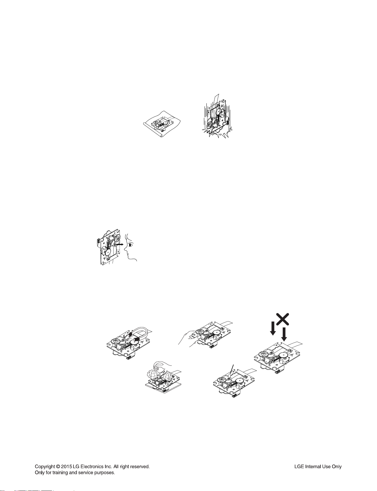
SERVICING PRECAUTIONS
NOTES REGARDING HANDLING OF THE PICK-UP
1. Notes for transport and storage
1) The pick-up should always be left in its conductive bag until immediately prior to use.
2) The pick-up should never be subjected to external pressure or impact.
Storage in conductive bag
Drop impact
2. Repair notes
1) The pick-up incorporates a strong magnet, and so should never be brought close to magnetic materials.
2) The pick-up should always be handled correctly and carefully, taking care to avoid external pressure and
impact. If it is subjected to strong pressure or impact, the result may be an operational malfunction and/or
damage to the printed-circuit board.
3) Each and every pick-up is already individually adjusted to a high degree of precision, and for that reason
the adjustment point and installation screws should absolutely never be touched.
4) Laser beams may damage the eyes!
Absolutely never permit laser beams to enter the eyes!
Also NEVER switch ON the power to the laser output part (lens, etc.) of the pick-up if it is damaged.
NEVER look directly at the laser beam, and don’t allow
contact with fingers or other exposed skin.
5) Cleaning the lens surface
If there is dust on the lens surface, the dust should be cleaned away by using an air bush (such as used
for camera lens). The lens is held by a delicate spring. When cleaning the lens surface, therefore, a cotton swab should be used, taking care not to distort lens.
Pressure
Magnet
How to hold the pick-up
Cotton swab
Conductive Sheet
6) Never attempt to disassemble the pick-up.
Spring has excess pressure. If the lens is extremely dirty, apply isopropyl alcohol to the cotton swab.
(Do not use any other liquid cleaners, because they will damage the lens.) Take care not to use too much
of this alcohol on the swab, and do not allow the alcohol to get inside the pick-up.
1-3
Pressure
Page 5
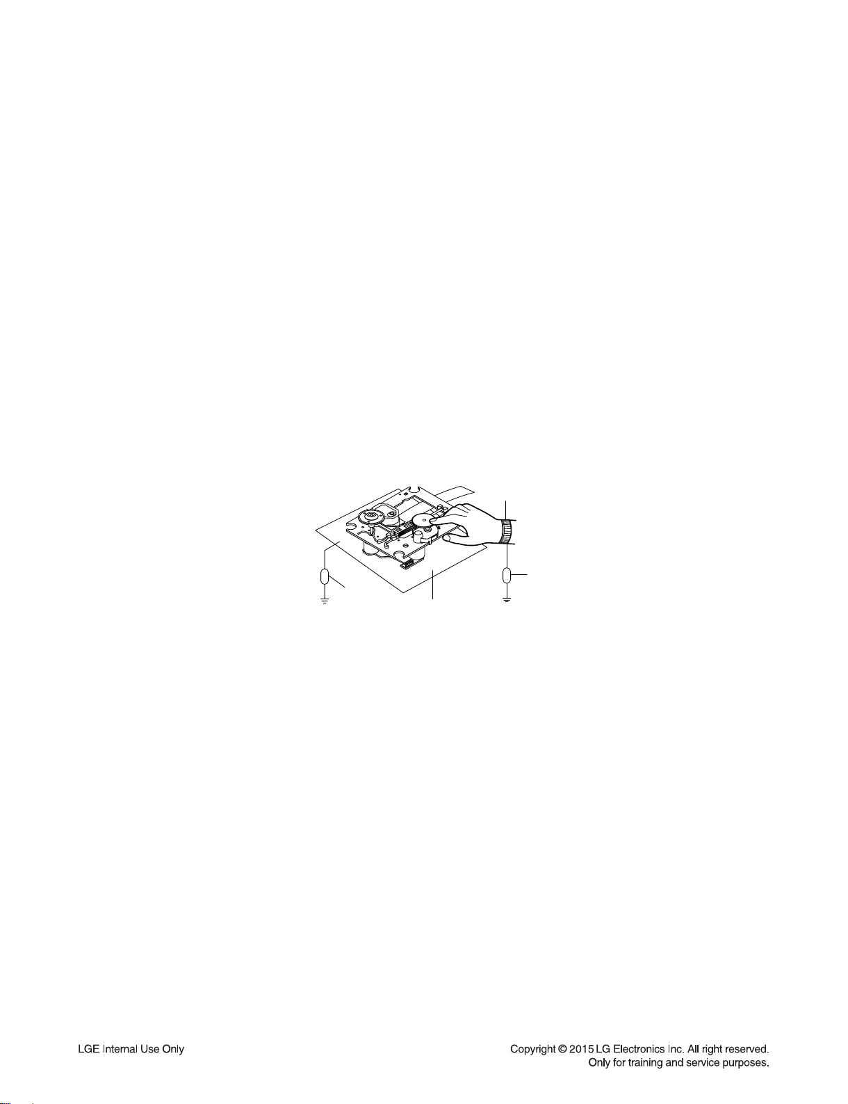
NOTES REGARDING COMPACT DISC PLAYER REPAIRS
1. Preparations
1) Compact disc players incorporate a great many ICs as well as the pick-up (laser diode). These components
are sensitive to, and easily affected by, static electricity. If such static electricity is high voltage, components
can be damaged, and for that reason components should be handled with care.
2) The pick-up is composed of many optical components and other high-precision components. Care must be
taken, therefore, to avoid repair or storage where the temperature or humidity is high, where strong magnetism is present, or where there is excessive dust.
2. Notes for repair
1) Before replacing a component part, first disconnect the power supply lead wire from the unit
2) All equipment, measuring instruments and tools must be grounded.
3) The workbench should be covered with a conductive sheet and grounded.
When removing the laser pick-up from its conductive bag, do not place the pick-up on the bag. (This is
because there is the possibility of damage by static electricity.)
4) To prevent AC leakage, the metal part of the soldering iron should be grounded.
5) Workers should be grounded by an armband (1 M)
6) Care should be taken not to permit the laser pick-up to come in contact with clothing, in order to prevent
static electricity changes in the clothing to escape from the armband.
7) The laser beam from the pick-up should NEVER be directly facing the eyes or bare skin.
Armband
Resistor
(1 M)
Resistor
(1 M)
Conductive
Sheet
1-4
Page 6
ESD PRECAUTIONS
Electrostatically Sensitive Devices (ESD)
Some semiconductor (solid state) devices can be damaged easily by static electricity. Such components
commonly are called Electrostatically Sensitive Devices (ESD). Examples of typical ESD devices are integrated
circuits and some field-effect transistors and semiconductor chip components. The following techniques should
be used to help reduce the incidence of component damage caused by static electricity.
1. Immediately before handling any semiconductor component or semiconductor-equipped assembly, drain off
any electrostatic charge on your body by touching a known earth ground. Alternatively, obtain and wear a
commercially available discharging wrist strap device, which should be removed for potential shock reasons
prior to applying power to the unit under test.
2. After removing an electrical assembly equipped with ESD devices, place the assembly on a conductive surface
such as aluminum foil, to prevent electrostatic charge buildup or exposure of the assembly.
3. Use only a grounded-tip soldering iron to solder or unsolder ESD devices.
4. Use only an anti-static solder removal device. Some solder removal devices not classified as "anti-static" can
generate electrical charges sufficient to damage ESD devices.
5. Do not use freon-propelled chemicals. These can generate electrical charges sufficient to damage ESD
devices.
6. Do not remove a replacement ESD device from its protective package until immediately before you are
ready to install it. (Most replacement ESD devices are packaged with leads electrically shorted together by
conductive foam, aluminum foil or comparable conductive materials).
7. Immediately before removing the protective material from the leads of a replacement ESD device, touch the
protective material to the chassis or circuit assembly into which the device will by installed.
CAUTION : BE SURE NO POWER IS APPLIED TO THE CHASSIS OR CIRCUIT, AND OBSERVE ALL OTHER
SAFETY PRECAUTIONS.
8. Minimize bodily motions when handing unpackaged replacement ESD devices. (Otherwise harmless motion
such as the brushing together of your clothes fabric or the lifting of your foot from a carpeted floor can generate
static electricity sufficient to damage an ESD device).
CAUTION. GRAPHIC SYMBOLS
THE LIGHTNING FLASH WITH APROWHEAD SYMBOL. WITHIN AN EQUILATERAL TRIANGLE, IS
INTENDED TO ALERT THE SERVICE PERSONNEL TO THE PRESENCE OF UNINSULATED
“DANGEROUS VOLTAGE” THAT MAY BE OF SUFFICIENT MAGNITUDE TO CONSTITUTE A RISK OF
ELECTRIC SHOCK.
THE EXCLAMATION POINT WITHIN AN EQUILATERAL TRIANGLE IS INTENDED TO ALERT THE
SERVICE PERSONNEL TO THE PRESENCE OF IMPORTANT SAFETY INFORMATION IN SERVICE
LITERATURE.
1-5
Page 7

HIDDEN KEY MODE
Push both Display key and Remote Control key to activate it for 5 seconds.
1. Disc Lock On/Off (CD Function Only Active)
Display Key : PLAY/PAUSE
Remote Control Key : STOP
2. Check Version and Option code
Display Key : PLAY/PAUSE
Remote Control Key : PLAY/PAUSE
You can change [Audio MCU Version <-> Audio EQ Version <-> EEPROM Option] by SKIP+/-.
3. Clear EEPROM
Display Key : PLAY/PAUSE
Remote Control Key : SKIP-
4. Edit EEPROM
Display Key : PLAY/PAUSE
Remote Control Key : SKIP+
You can edit 0~f by Sound Effect or STOP key.
5. Amp Clip On/Off
Display Key : PLAY/PAUSE
Remote Control Key : Mute
Amp Clip Mode Change (Amp Clip On --> Amp Clip).
1-6
Page 8
SERVICE INFORMATION FOR EEPROM
POWER ON
FLD no disc status or AUX status.
Display ‘Play/Pause’ + Remote Control ‘Forward skip’
push same timing during 5 seconds.
FLD ‘OP00-00’
Move to appropriate position and make changes
with remote control ‘skip, sound effect, stop’ key.
Press ‘PLAY/PAUSE’ key.
FLD ‘write ok’
Display ‘Play/Pause’ + Remote Control ‘Forward skip’
push same timing during 5 seconds.
FLD ‘E2P CLR’
Completed
1-7
Page 9

PROGRAM DOWNLOAD & UPDATE GUIDE
Caution:
• When downloading the fi le, you should neither unplug the USB device, change to the other function,
nor power off the device.
• USB device must be unplugged when the downloading process is completed.
If security program (Water Wall) is activated on your PC, you must save the fi le to the USB storage device and
disable the security software, then download the fi le to your set.
1. Main Program
1) File name is CM4360_FW_yymmddNo.bin
2) Put upgrade fi le into USB root directory. (No other fi le exist on root directory)
3) Change the mode to USB mode.
4) It will start update process automatically with showing “MCU UP” on Display window.
5) If the update is fi nished, the set will turn off automatically.
2. EQ Program
1) File name is EQ_PRG_CM4360_yymmdd_No_Checksum.bin
2) Put upgrade fi le into USB root directory. (No other fi le exist on root directory)
3) Change the mode to USB mode.
4) It will start update process automatically with showing “EQ UP” on Display window.
5) If the update is fi nished, the set will turn off automatically.
1-8
Page 10

SPECIFICATIONS
• GENERAL
Power requirements Refer to the main label.
Power consumption Refer to the main label.
Networked standby : 0.4 W
(If all network ports are activated.)
Dimensions (W x H x D) Approx. 204.5 mm x 278 mm x 285.5 mm
Net Weight Approx. 2.53 kg
Operating temperature 5 °C to 35 °C
Operating humidity 5 % to 90 %
• INPUTS
Analog audio in (AUX IN) 2.0 Vrms (1 kHz, 0 dB), 75 Ω, RCA jack (L, R) x 1
• TUNER
FM Tuning Range 87.5 to 108.0 MHz or 87.50 to 108.00 MHz
• AMPLIFIER (RMS OUTPUT POWER)
THD 20 %
Total 230 W
Front 115 W X 2 (4 Ω at 1 kHz)
• SYSTEM
Frequency response 100 to 20 000 Hz
Signal-to-noise ratio 75 dB
Dynamic range 75 dB
Bus Power Supply (USB) 5 V 500 mA
USB Version 2.0
FRONT SPEAKERS
•
Type 2 Way 2 Speaker
Impedance 4 Ω
Rated Input Power 115 W
Max. Input Power 230 W
Dimensions (W x H x D) Approx. 203 mm x 284.5 mm x 200 mm
Net Weight Approx. 2.1 kg
• Design and specifications are subject to change without notice.
1-9
Page 11
1-10
Page 12

SECTION 2
CABINET & MAIN CHASSIS
CONTENTS
EXPLODED VIEWS ........................................................................................................................................... 2-3
1. CABINET AND MAIN FRAME SECTION ................................................................................................. 2-3
2. PACKING ACCESSORY SECTION ......................................................................................................... 2-7
3. SPEAKER SECTION ................................................................................................................................ 2-8
2-1
Page 13

2-2
Page 14
DISPLAY
MAIN
SMPS
A
B
C
C
H
H
E
B
G
F
A
E
D
F
D
G
I
CABLE3
CABLE4
B/T
A52
263
CABLE5
492
492
492
254
251
252
253
255
256A
258A
257A
258B
257B
256B
492259
512
CABLE1
CABLE2
A26
511
452
A43
505
262
A46
505
505
A47
492265
492492
492492
492264
261
452
505
459
260
459
505
505
825
266
EXPLODED VIEWS
1. CABINET AND MAIN FRAME SECTION
NOTES) THE EXCLAMATION POINT WITHIN AN
EQUILATERAL TRIANGLE IS INTENDED
TO ALERT THE SERVICE PERSONNEL
TO THE PRESENCE OF IMPORTANT
SAFETY INFORMATION IN SERVICE
LITERATURE.
I
300
Page 15
Page 16
2. PACKING ACCESSORY SECTION
801 Owner’s manual
808 Battery
804 Bag
803 Packing
900 Remote Control
803 Packing
802 Box
Page 17
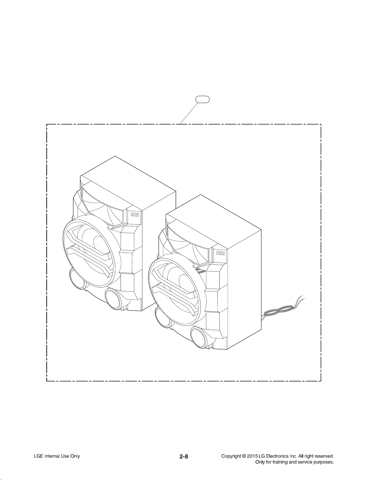
3. SPEAKER SECTION
A60
Page 18

SECTION 3
ELECTRICAL
CONTENTS
ONE POINT REPAIR GUIDE ............................................................................................................................ 3-2
1. NO POWER ............................................................................................................................................ 3-2
2. NO BOOTING WHEN POWER ON THE SET........................................................................................ 3-4
3. VFD IS NOT DISPLAYED WHEN POWER ON THE SET ..................................................................... 3-5
4. NO OPERATION OF MD ........................................................................................................................ 3-6
5. NO SOUND ........................................................................................................................................... 3-11
ELECTRICAL TROUBLESHOOTING GUIDE ................................................................................................. 3-16
1. POWER (SMPS) ................................................................................................................................... 3-16
2. MCS PART CHECK .............................................................................................................................. 3-19
3. FLD DISPLAY CHECK ......................................................................................................................... 3-20
4. PWM MODULATION CHECK ............................................................................................................... 3-21
5. POWER AMP PART CHECK ............................................................................................................... 3-22
6. TUNER / AUX FUNCTION CHECK ...................................................................................................... 3-23
7. TUNER FUNCTION CHECK................................................................................................................. 3-24
8. CD FUNCTION CHECK ........................................................................................................................ 3-25
9. DOUBLE USB FUNCTION ................................................................................................................... 3-26
WAVEFORMS OF MAJOR CHECK POINT .................................................................................................... 3-27
1. SDRAM ................................................................................................................................................. 3-27
2. SERVO .................................................................................................................................................. 3-27
3. AUDIO PATH ........................................................................................................................................ 3-28
4. USB ....................................................................................................................................................... 3-29
WIRING DIAGRAM .......................................................................................................................................... 3-31
BLOCK DIAGRAMS ........................................................................................................................................ 3-33
1. SYSTEM BLOCK DIAGRAM ................................................................................................................ 3-33
2. SMPS BLOCK DIAGRAM ..................................................................................................................... 3-35
3. POWER BLOCK DIAGRAM ................................................................................................................. 3-37
CIRCUIT DIAGRAMS ...................................................................................................................................... 3-39
1. SMPS CIRCUIT DIAGRAM .................................................................................................................. 3-39
2. MAIN - POWER CIRCUIT ..................................................................................................................... 3-41
3. MAIN - SERVO CIRCUIT DIAGRAM .................................................................................................... 3-43
4. MAIN - MPEG CIRCUIT DIAGRAM ...................................................................................................... 3-45
5. MAIN - DSP, AMP CIRCUIT DIAGRAM ............................................................................................... 3-47
6. MAIN - TUNER, FUNCTON, AUDIO AMP, A/D CIRCUIT DIAGRAM .................................................. 3-49
7. DISPLAY CIRCUIT DIAGRAM ............................................................................................................. 3-51
CIRCUIT VOLTAGE CHART ........................................................................................................................... 3-53
1. ICs ......................................................................................................................................................... 3-53
2. CAPACITORS ....................................................................................................................................... 3-55
PRINTED CIRCUIT BOARD DIAGRAMS ....................................................................................................... 3-57
1. SMPS P.C.BOARD ............................................................................................................................... 3-57
2. MAIN P.C.BOARD ................................................................................................................................ 3-59
3. DISPLAY P. C. BOARD ........................................................................................................................ 3-63
3-1
Page 19

ONE POINT REPAIR GUIDE
AC i
n 110~240
V
12
34
LF901
UM-007/UF16-45
1. NO POWER
If the unit doesn’t work by no power problem, repair the set according to the following guide.
1-1. FUSE & BRIDGE DIODE
1-1-1. Solution
Please check and replace F900, BD900 or TH900 on SMPS board.
1-1-2. How to troubleshoot (Countermeasure)
1) Check if the fuse F900 is open or short-circuit.
2) Check if the bridge diode BD900 is short-circuit by over current with a digital multi meter.
3) Check if the NTC thermistor TH900 is normal or open.
1-1-3. Service hint (Any picture/ Remark)
21
LF900
UM-007/UF16-45
T3.15AL 250V
F900
12
1
2
VH-3Y
PN900
LN
43
1
BD900
2
KB406
TH900
5D-9
3
HVCC
IN4007
D910
+
C905
22uF/450V
IC904
DRAIN
7
GND
OB2338
DRAIN
R914
6
5
PWM
1
VFB
GND_EARTH
VCC
SENSE
3
ZD90318V 0.5W NC
R911 0R
4
R948
R949
C907 0.1uF/50V
2.2/1206
2.2/1206
VCC_G
2
1K
R947
CY902 471/250V
4
CM901
0.1uF/275V
CY903 471/250V
< F900 >
If F900 is not short-circuit,
replace it with a same
specifi cations one.
< BD900 >
If BD900 is short-circuit,
replace it with a new one.
3-2
< TH900 >
If TH900 is open,
replace it with a new one.
Page 20

ONE POINT REPAIR GUIDE
Powe r ON
Powe r OFF
NO POWER
If the unit doesn’t work by no power problem, repair the set according to the following guide.
1-2. D907
1-2-1. Solution
Please check and replace D907 on SMPS board.
1-2-2. How to troubleshoot (Countermeasure)
1) Check the anode-cathod voltage of D907 with a digital multi-meter, it is normally 0.2 ~ 0.3 V.
If it doesn’t have any voltage, it’s destroyed. Replace it with a new one.
1-2-3. Service hint (Any picture/ Remark)
FB901
C918
100pF/1KV
M_VCC
R956
10R
ND_EARTH
C908 22uF/50V
T900
R954
+
C919
220uF/25V
0.1uF/50V
C922 1000uF/16V
C938
C926 0.1uF/X7R
2010
2.2R 3/4W
L900
R928 1k
C920
+
47uF/25V
10uH/2A
R980
100K
R950 10K
+5.2V
470uF/16V
+
C924
C923 0.1uF/50V
R926 10k/1%
470pF/1kV
D907
SR360
C925
470pF/100V
D906
HER103
C902
R924
5.1R/1206
R925
R927 10K
R901
5.1R/1206
+
330
5
200K/0.5W
200K/O.5W
R906
R955
BEAD
D901
FR107
102pF/630V
C906
4
3
6
9
D903
FR107
+
15V 0.5W
ZD901
R910
2.2R/1206
2
EE19
4
3
PC900
CY905 471/250V
71
EL817
1
2
IC902
TL431
1
23
< SMPS schematic diagram >
3-3
R929 9.1k/1%
Page 21

ONE POINT REPAIR GUIDE
KEY1 (R131)
PWR_CTRL (R149)
IC105
2. NO BOOTING WHEN POWER ON THE SET
The set doesn’t work when press the power button on the display board or the remote control.
2-1. FLASH MEMORY
2-1-1. Solution
Please check and replace IC105 on MAIN board.
2-1-2. How to troubleshoot (Countermeasure)
1) Check 5.1 V to PN200 in standby mode.
If there is no 5.1 V, check the SMPS.
2) Check 12 V, 5.1 V and PVDD when power on the set.
-
If the set doesn’t work regardless of what the KEY1 (R131) changes high to low while pressing the power button.
X100 and X101 work normally but, if you can not power on the set, replace IC105 with a new one on the
MAIN board.
2-1-3. Service hint (Any picture/ Remark)
KEY1 (R131)
IC105
< Signal check point >
3-4
PWR_CTRL (R149)
Page 22

ONE POINT REPAIR GUIDE
3. VFD IS NOT DISPLAYED WHEN POWER ON THE SET
When power on the set, any icons or characters on VFD are not displayed.
3-1. VFD
3-1-1. Solution
Please check and replace VFD300 on DISPLAY board.
3-1-2. How to troubleshoot (Countermeasure)
1) Check if VKK, FL+ and FL- are output from SMPS to VFD via the MAIN board.
2) Check if IC105 outputs VFD_SDA, VFD_CLK and VFD_STB to the DISPLAY board.
3) Check the GR signal(pulse signal) of IC300 on the DISPLAY board.
Check the SG signal(pulse signal) of IC300 on the DISPLAY board.
If the GR and SG signal isn’t output, replace IC300 with a new one.
If the GR and SG signal is output, replace VFD300 with a new one.
3-1-3. Service hint (Any picture/ Remark)
SG signal
SEG10
SEG11
SEG12
SEG13
SEG14
SEG15
SEG16
F-VKK
R301
C331
C300
C307
0.1uF
100K
0.1uF
47uF/50V
GND GND
GND
VDD+3.3V
GR signal
23
24
25
26
27
28
29
30
31
32
33
SG10
SG11
SG12
SG13
SG14
SG15
SG16/KS16
VEE
SG17/GR12
GR11
GR10
SEG9
GND
13
14
SG115SG216SG317SG418SG519SG620SG721SG822SG9
VDD112VSS1
DOUT
LDE4
VOL_LDE3
VOL_LDE2
VOL_LDE1
GR438GR537GR636GR735GR834GR9
GR341GR242GR143VDD44VSS
39
40
C301
0.1uF
GD1
GD2
GD3
GD4
GD5
GD6
GD7
GD8
VDD+3.3V
C332
C315
0.1uF
47uF/16V
GND
GND
100K
R307
K2
11
K1
10
P-STB
STB
9
P-CLK
CLK
8
P-SDA
DIN
7
6
R302
OSC
5
4
3
2
1
IC300
PT6315
GND
VDD+3.3V
GND
100K
R306
GND
220R
R305
220R
R304
220R
R303
100P
100K
GND
C308
100P
100P
C317
C309
GND GND
VFD-STB
VFD-CLK
VFD-SDA
GND
GR SIGNAL
ABOUT 30 V
SEG1
SEG2
SEG3
SEG4
SEG5
SEG6
SEG7
SEG8
SG SIGNAL
ABOUT 30 V
3-5
< Waveform of GR and SG signal >
Page 23

ONE POINT REPAIR GUIDE
SP+
pin17 to PN801
SP-
pin18 to PN801
IC801
4. NO OPERATION OF MD
When no sound output in the CD function, you can not listen to music reading data from a CD disc
if the servo motors in MD don’t work. This step is for checking the SPINDLE MOTOR among them.
4-1. SPINDLE MOTOR
4-1-1. Solution
Please check and replace IC800, IC801 on MAIN board.
4-1-2. How to troubleshoot (Countermeasure)
1) Check the CLVOUT signal from pin16 of IC800.
If no signal, check 3.3 V (pin63 RF) and X800.
2) Check the SPIN- & SPIN+ from IC801 to PN801 for driving SPINDLE motor. It is about 3.6 Vp-p.
If no signal, check +5 V for IC800.
3) Check if the cable is solidly connected between PN801 and MD.
4) Check the MD.
If the spindle motor is sort-circuit or has any trouble, it can not rotate CD discs.
Please check the function after changing another MD.
4-1-3. Service hint (Any picture/ Remark)
About 3.6 Vp-p
< Waveform of SP- & SP+
for driving SPINDLE motor >
SP-
pin18 to PN801
IC801
< Signal check point >
SP+
pin17 to PN801
3-6
Page 24

ONE POINT REPAIR GUIDE
SLED+
pin11 to PN801
SLED-
pin12 to PN801
IC801
NO OPERATION OF MD
When no sound output in the CD function, you can not listen to music reading data from a CD disc
if the servo motors in MD don’t work. This step is for checking the SLED MOTOR among them.
4-2. SLED MOTOR
4-2-1. Solution
Please check and replace IC800, IC801 on MAIN board.
4-2-2. How to troubleshoot (Countermeasure)
1) Check the SDOUT signal from pin15 of IC800.
If no signal, check 3.3 V (pin36 RF) and X800.
2) Check the SLED+ & SLED- from IC801 to PN801 for driving SPINDLE motor. It is about 2.9 Vp-p.
If no signal, check +5 V for IC801.
3) Check if the cable is solidly connected between PN801 and MD.
4) Check the MD.
If the sled motor is sort-circuit or has any trouble, it can not move the pickup module.
Please check the function after changing another MD.
4-2-3. Service hint (Any picture/ Remark)
SL- TO CN405
SL+ TO CN405
< Waveform of SLED- & SLED+
for driving SLED motor >
IC801
SLED+
pin11 to PN801
< Signal check point >
SLED-
pin12 to PN801
3-7
Page 25

ONE POINT REPAIR GUIDE
LOAD+
pin9 to PN801
LOAD-
pin10 to PN801
MOT_OPEN
pin7 to PN801
MOT_CLOSE
pin8 to PN801
IC801
NO OPERATION OF MD
When no sound output in the CD function, you can not listen to music reading data from a CD disc if
the servo motors in MD don’t work. This step is for checking the TRAY OPEN/CLOSE MOTOR among
them.
4-3. TRAY OPEN/CLOSE MOTOR
4-3-1. Solution
Please check and replace IC105, IC801 on MAIN board.
4-3-2. How to troubleshoot (Countermeasure)
1) Check MOT_OPEN & MOT_CLOSE signals from pin”K4, L4” of IC105 to IC801.
If no signal, check + 5 V to IC801.
2) Check LOAD± from IC801 to PN802 for driving the tray open/close motor. It is about 3.85 Vp-p.
If no signal, check +5 V to IC801. If it has any trouble, replace it with a new one.
3) Check if the cable is solidly connected between PN802 and MD.
4) Check the MD.
If the tray motor is sort-circuit or has any trouble, it can not open or close the tray.
Please check the function after changing another MD.
4-3-3. Service hint (Any picture/ Remark)
MOT_OPEN
CLOSE
LO- TO PN801
LO+ TO PN801
< Waveform for driving
TRAY open/close motor >
LOAD+
pin9 to PN801
IC801
MOT_OPEN
pin7 to PN801
LOAD-
pin10 to PN801
MOT_CLOSE
pin8 to PN801
< Signal check point >
3-8
Page 26

ONE POINT REPAIR GUIDE
TR+
pin16 to PN801
TR-
pin15 to PN801
IC801
NO OPERATION OF MD
When no sound output in the CD function, you can not listen to music reading data from a CD disc if
the pickup module in MD doesn’t work. This step is for checking the LASER TRACKING ACTUATOR.
4-4. LASER TRACKING ACTUATOR
4-4-1. Solution
Please check and replace IC800, IC801 on MAIN board.
4-4-2. How to troubleshoot (Countermeasure)
The tracking actuator makes the laser beam be positioned in the center of a track on CD disc.
1) Check the TDOUT signal from pin14 of IC801.
If no signal, check 3.3 V (pin63 RF) and X800.
2) Check TR- & TR+ from IC801 to PN800 for driving the tracking actuator.
If no signal, check +5 V for IC801.
3) Check if the FFC cable is solidly connected between PN800 and MD.
4) Check the MD.
If the pickup module has any trouble, it can not move the laser beam on the left or right side.
Please check the function after changing another MD.
4-4-3. Service hint (Any picture/ Remark)
< Waveform of TR±
for driving TRACKING actuator >
TR+
pin16 to PN801
IC801
< Signal check point >
TR-
pin15 to PN801
3-9
Page 27
ONE POINT REPAIR GUIDE
F+
pin14 to PN801
F-
pin13 to PN801
IC801
NO OPERATION OF MD
When no sound output in the CD function, you can not listen to music reading data from a CD disc if
the pickup module in MD doesn’t work. This step is for checking the LASER FOCUSING ACTUATOR.
4-5. LASER FOCUSING ACTUATOR
4-5-1. Solution
Please check and replace IC800, IC801 on MAIN board.
4-5-2. How to troubleshoot (Countermeasure)
The focusing actuator makes the laser beam keep a regular interval with the surface of a CD disc.
1) Check the BUSY signal from pin21 of IC800.
If no signal, check 3.3 V (pin63 RF) and X800.
2) Check F- & F+ from IC801 to PN800 for driving the focusing actuator.
If no signal, check +5 V for IC801.
3) Check if the FFC cable is solidly connected between PN800 and MD.
4) Check the MD.
If the pickup module has any trouble, it can not move the laser beam on the top or bottom side.
Please check the function after changing another MD.
4-5-3. Service hint (Any picture/ Remark)
< Waveform of F±
for driving FOCUSING actuator >
IC801
F-
pin13 to PN801
< Signal check point >
F+
pin14 to PN801
3-10
Page 28

ONE POINT REPAIR GUIDE
5. NO SOUND
There is no sound output in the CD FUNCTION, repair the set according to the following guide.
5-1. IN THE CD FUNCTION
5-1-1. Solution
Please check and replace IC105, IC700 on MAIN board.
5-1-2. How to troubleshoot (Countermeasure)
1) Check CD_BCLK, CD_LRCK, & CD_DATA signals from IC800 to IC105.
If no signal, check if the RF & servo signals from MD is entered to IC105.
Refer to the “No operation of MD” guide on Item 4.
2) Check the following I2S signal flow. < I2S audio signal Interface >
- MCS_TX_BCK: IC105_pin”E1” -> IC400_pin12
- MCS_TX_LRCK: IC105_pin”D1” -> IC400_pin10 (44.1 kHz)
- MSC_TX_ADATAO: IC105_pin”E2” -> IC400_pin9
- MSC_RX_MCLK: IC105_pin”D2” -> IC400_pin11
If there is any trouble, check the power for each IC. The power is normal but, if the signal waveform to
the IC is distorted or no signal, replace it with a new one.
3) Check if “Digital audio AMP block” on Item 5-2 is normal.
5-1-3. Service hint (Any picture/ Remark)
P/UP
IC800
DSP
BU9546
M
176PIN BGA
IC105
MLC3730
MCS_MCLK (16.93 MHz)
MCS_BCK(1.4 MHz)
MCS_ADAT_OUT
MCS_LRCK(44.1 KHz)
USB 2.0 OTG
Main Processor
USB 1.1
16KB
ARM
Host/Device
I-Cache
926EJS
16KB
400Mhz
SRAM (10K)
D-Cache
SDRAM
Controller
Boot ROM (20KB)
Interrupt
controller
CDROM x8 speed
Decoder
ADC (12bit*5ch)
GDMA 3ch
Timer, Watchdog
GPIO (72 Max)
NAND Controller
within BCH codec
SPI 4ch (Max)
14bits ECC
FR,FL
ZHM6 775.42
TAS5612LA
DSP
Audio DSP-0
133Mhz
SRAM29KB
DSP
I-Cache 8KB
133Mhz
D-Cache 8KB
GDMA 2ch
SPDIF (Rx, Tx)
RTC & Wake up
Clock Controller
UART 4ch (Max)
Reset Controller
I2C 2ch
Test Controller
SDHC-SDIO 4ch (Max)
Audio DSP-1
SRAM29KB
I-Cache 8KB
D-Cache 8KB
I2S (7.1ch)
ADPCM
PLL
< Waveform of I2S audio interface signals >
PWM
068 9SP
< I2S Signal Flow >
3-11
Page 29

ONE POINT REPAIR GUIDE
L702
L701
L704
L703
IC701
IC700
NO SOUND
There is no sound output by DIGITAL AUDIO AMP DAMAGE, repair the set according to the following
guide.
5-2. BY DIGITAL AUDIO AMP DAMAGE (IN ALL FUNCTIONS)
5-2-1. Solution
Please check and replace IC700, IC701 on MAIN board.
5-2-2. How to troubleshoot (Countermeasure)
1) Check FR_P/N, FL_P/N signals from IC700 to IC701 each input function.
If no signal, check if I2S audio signals are entered to IC700.
Refer to “I2S audio signal interface” on Item 5-1.
2) Check PVDD.
If PVDD is abnormal, check the SMPS.
3) Check +12 V for driving the gate of AMP IC.
a. All the powers are normal, but if +12 V is low, there is possible for AMP IC to be damaged.
b. Remove L701, L702, L703 and L704 one by one.
When removed a inductance, if +12 V is recovered, the IC connected to it was damaged.
c. Replace the IC with a new one.
4) Check the impedance between IC701 OUT_A, OUT_B and GND.
a. If the impedance is 0 Ω, the IC must be damaged.
b. After removing the heat sink, replace it with a new one.
5-2-3. Service hint (Any picture/ Remark)
L702
L701
IC701
L704
L703
IC700
< Signal check point >
3-12
Page 30

ONE POINT REPAIR GUIDE
NO SOUND
There is no sound output in the USB FUNCTION, repair the set according to the following guide.
5-3. IN THE USB FUNCTION
5-3-1. Solution
Please check and replace IC105 on MAIN board and DISPLAY board.
5-3-2. How to troubleshoot (Countermeasure)
1) Check +5V_USB to DISPLAY board.
If the USB LED are turned on, the voltage is okay, if so not, check +5.1V of PN104.
2) Check USB D+,- from MAIN board to DISPLAY board.
a. Check USB± signals to PN104 (pin2, 3).
If there is any trouble, check the power for each IC. The power is normal but , if the signal waveform
to the IC is distorted or no signal, replace it with a new one.
3) Check if “Digital audio AMP block” on item 5-2 is normal.
5-3-3. Service hint (Any picture/ Remark)
DSP IC105
MLC3730S
176PIN BGA
USB 2.0 OTG
Main Processor
16KB
ARM
I-Cache
926EJS
16KB
400Mhz
D-Cache
Boot ROM (20KB)
ADC (12bit*5ch)
Timer, Watchdog
GPIO (72 Max)
SPI 4ch (Max)
PWM
Audio DSP-0
SRAM29KB
DSP
I-Cache 8KB
133Mhz
D-Cache 8KB
GDMA 2ch
RTC & Wake up
UART 4ch (Max)
I2C 2ch
SDHC-SDIO 4ch (Max)
ZHM 6 75.42
06 8 9SP
USB 1.1
Host/Device
SRAM (10K)
SDRAM
Controller
Interrupt
controller
CDROM x8 speed
Decoder
GDMA 3ch
NAND Controller
within BCH codec
14bits ECC
Audio DSP-1
SRAM29KB
DSP
I-Cache 8KB
133Mhz
D-Cache 8KB
I2S (7.1ch)
SPDIF (Rx, Tx)
ADPCM
PLL
Clock Controller
Reset Controller
Test Controller
FR,FL
USB1_D±
USB2_D±
TAS5612LA
D- to pin2 of PN104
D+ to pin3 of PN104
< Waveform of USB D± signal >
< USB function signal fl ow >
3-13
Page 31

ONE POINT REPAIR GUIDE
NO SOUND
There is no sound output in the AUX FUNCTION, repair the set according to the following guide.
5-4. IN THE AUX FUNCTION
5-4-1. Solution
Please check and replace IC400 on MAIN board.
5-4-2. How to troubleshoot (Countermeasure)
1) Check AUDIO_RIN, AUDIO_LIN signals to IC400 pin1, 2.
2) Check if MCS_TX_BCK, MCS_RX_MCLK and MCS_TX_LRCK are entered from IC105 to IC400.
3) Check if MCS_RX_ADATA is entered from IC400 to IC105.
If no signal, check +3.3 V (ADC) for IC400. If is NG, replace it a new one.
4) Check the following I2S signal flow from IC105 to IC700. (Refer to Item 5-1.)
If there is any trouble, check the power for each IC. The power is normal but, if the signal waveform to
the IC is distorted or no signal, replace it with a new one.
5) Check if the digital audio AMP block is okay. Refer to “Digital Audio AMP” guide on Item 5-2.
If AMP is damaged, replace it with a new one.
5-4-3. Service hint (Any picture/ Remark)
AUX
AUX _L /R
IC700
PWM
PS9 860
IC403 CD4052
IC401 CD4558
IC400 CJC5357
ZHM 6 75.42
FR,FL
DSP IC105
MLC3730S
176PIN BGA
USB 2.0 OTG
Main Processor
16KB
ARM
I-Cache
926EJS
16KB
400Mhz
D-Cache
Boot ROM (20KB)
ADC (12bit*5ch)
Timer, Watchdog
GPIO (72 Max)
SPI 4ch (Max)
Audio DSP-0
DSP
133Mhz
GDMA 2ch
RTC & Wake up
UART 4ch (Max)
SDHC-SDIO 4ch (Max)
USB 1.1
Host/Device
SRAM (10K)
SDRAM
Controller
Interrupt
controller
CDROM x8 speed
Decoder
GDMA 3ch
NAND Controller
within BCH codec
14bits ECC
TAS5612L
SRAM29KB
I-Cache 8KB
D-Cache 8KB
I2C 2ch
3-14
< Signal check point >< AUX function signal fl ow >
Page 32

ONE POINT REPAIR GUIDE
TUN_L to C435
TUN_R to C434
IC402
NO SOUND
There is no sound output in the TUNER FUNCTION, repair the set according to the following guide.
5-5. IN THE TUNER FUNCTION
5-5-1. Solution
Please check and replace IC400, IC402 on MAIN board.
5-5-2. How to troubleshoot (Countermeasure)
1) Check if TUL_L/R is entered from pin13, 14 of IC402 to IC403 pin1, 12.
If no signals, check +3.3 V for tuner power.
Check if the TUNER control signals (TUN_RST, TUN_SDA AND TUN_SCL) are entered from IC105 to IC402
If it doesn’t work, replace TUNER with a new one.
2) Check if MCS_TX_BCK, MCS_RX_MCLK and MCS_TX_LRCK are entered from IC105 to IC400.
3) Check if MCS_RX_ADATA is entered from IC400 to IC105.
If no signal, check +3.3 V (ADC) for IC400. If is NG, replace it with a new one.
4) Check the following I2S audio signal flow from IC105 to IC700. (Refer to Item 5-1.)
If there is any trouble, check the power for each IC. The power is normal but, if the signal waveform to
the IC is distorted or no signal, replace it with a new one.
5) Check if the digital audio AMP block is okay. Refer to “Digital Audio AMP” guide on Item 5-2.
If AMP is damaged, replace it with a new one.
5-5-3. Service hint (Any picture/ Remark)
TUNER
TU_L /R
IC700
PWM
PS9 860
IC402 Si4702
IC403 CD4052
IC401 CD4558
IC400 CJC5357
ZHM 6 75.42
FR,FL
DSP IC105
MLC3730S
176PIN BGA
USB 2.0 OTG
Main Processor
16KB
ARM
I-Cache
926EJS
16KB
400Mhz
D-Cache
Boot ROM (20KB)
ADC (12bit*5ch)
Timer, Watchdog
GPIO (72 Max)
SPI 4ch (Max)
Audio DSP-0
DSP
133Mhz
RTC & Wake up
UART 4ch (Max)
SDHC-SDIO 4ch (Max)
USB 1.1
Host/Device
SRAM (10K)
SDRAM
Controller
Interrupt
controller
CDROM x8 speed
Decoder
GDMA 3ch
NAND Controller
within BCH codec
14bits ECC
TAS5612L
SRAM29KB
I-Cache 8KB
D-Cache 8KB
GDMA 2ch
I2C 2ch
TUN_L to C435
IC402
TUN_R to C434
< TUNER IN function signal fl ow >
< Signal check point >
3-15
Page 33

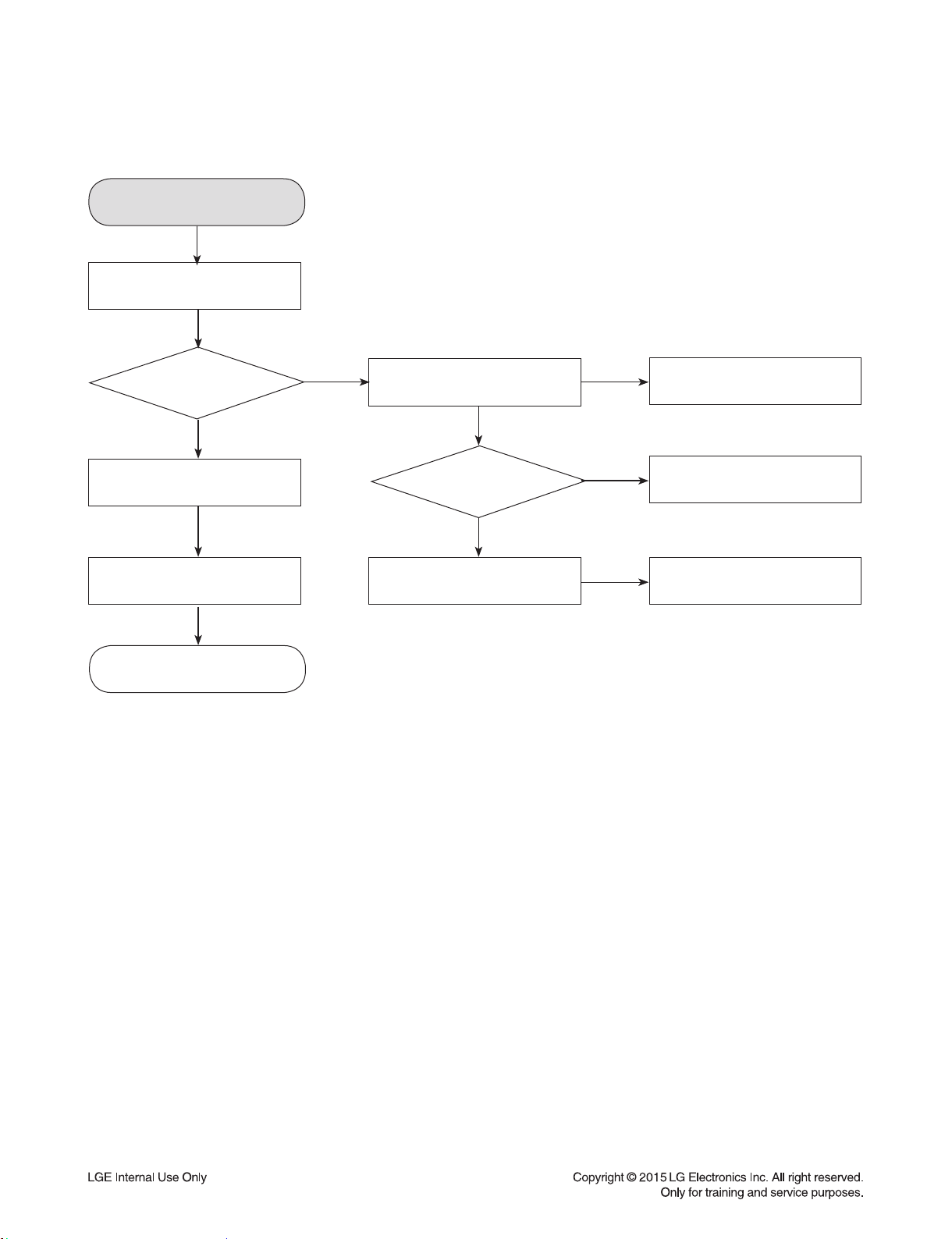
ELECTRICAL TROUBLESHOOTING GUIDE
1. POWER (SMPS)
No 5.1 VA
YES
F900 normal?
YES
BD900 normal?
YES
TH901(TH900) normal?
YES
Is Vcc
(10 V ~ 18 V) supplied to
IC904 pin3?
YES
D906 normal?
NO
Replace F900 (Use the same fuse).
NO
Replace BD900.
NO
Replace TH900.
NO
D903 normal?
NO
Check or replace D903.
NO
Replace D906.
YES
Is there
about 2.5 V at
IC902 pin1?
YES
D907 normal?
YES
Power line of main PCB is short.
NO
Replace IC902.
NO
Replace D907.
3-16
Page 34

ELECTRICAL TROUBLESHOOTING GUIDE
No PVDD (28 V)
YES
F900 normal?
YES
BD900 normal?
YES
TH900 normal? Replace TH900.
YES
NO
NO
NO
Replace F900 (Use the same fuse).
Replace BD900.
(14 V ~ 26 V) supplied to
Is Vcc
IC901 pin6?
YES
IC901 normal? Replace IC901.
YES
D908 normal?
NO
NO
NO
D903 normal?
YES
Q901 base HIGH?
YES
Check or replace Q901.
Replace D908.
NO
Check or replace D903.
NO
•
Check P_CTRL HIGH signal from MCS.
• Check PC902.
YES
Is there about 2.5 V
at IC903 pin1?
YES
Power line of main PCB is short.
NO
Replace IC903.
3-17
Page 35

ELECTRICAL TROUBLESHOOTING GUIDE
No 12 V
YES
Is Vcc (12 V)
supplied to D906?
YES
Q905 pin2 “HIGH”?
YES
Check or replace IC905.
No VFD
YES
Is VFD (5 V)
supplied to PN100 pin1?
NO
NO
Check or replace D906.
Check P_CTRL HIGH signal from MCS.
YES
D301 normal?
YES
D302 normal?
YES
Q301/ Q303/ Q305/ Q306 normal?
YES
Check or replace VFD.
NO
NO
NO
3-18
Check or replace D301.
Check or replace D302.
Check or replace Q301/ Q303/ Q305/ Q306.
Page 36

ELECTRICAL TROUBLESHOOTING GUIDE
2. MCS PART CHECK
MCS PART CHECK
YES
Check if voltage
of PN200 pin8 is 5.1 VA.
YES
Check if IC204
have 3.3 V output.
YES
Check if IC205
have 1.2 V output.
YES
X100: 32.768 kHz, X101: 24 MHz
Check the operation.
YES
NO
Refer to SMPS troubleshooting.
NO
Check and change IC204.
NO
Check and change IC205.
OK
3-19
Page 37

ELECTRICAL TROUBLESHOOTING GUIDE
3. FLD DISPLAY CHECK
FLD DISPLAY CHECK
YES
Check
PN100 pin1 input
voltage 5 V.
YES
Check D301
input votltage 5 V?
YES
pin6, 7 Output votltage AC 2.6 V.
Check T300
Check D302 pin1 Output
votltage -27 V.
YES
Check
IC300(PT6315) voltage
pin30 VKK: -27 V
pin13, 43: 3.3 V.
YES
NO
NO
NO
NO
Refer to SMPS/MPEG
troubleshooting.
Check and change D300.
Check and change
Q301, Q303, Q305, Q306.
If voltage is not 3.3 V.
YES
Check IC300.
NO
Replace IC300.
Check IC300
data communication
STB/DATA/CLK.
YES
FLD light on?
YES
OK
NO
YES
OK
Check input data
PN100 pin6, 7, 8.
YES
Check output data R304 R305
R303.
YES
Check IC300.
YES
OK
3-20
NO
NO
Refer to MPEG troubleshooting.
Replace IC300.
Page 38

ELECTRICAL TROUBLESHOOTING GUIDE
4. PWM MODULATION CHECK
PWM MODULATION PART
CHECK
YES
Check
PN200 pin8
(5.1 V)
YES
• Check IC700 (PS9860) VDD 3.3 V - pin6,17, 34, 43, 52.
• Check X601 (12.288 MHz).
YES
Check
X700(24.576 MHz)
operation.
YES
Check IC700 pin8 SCL input.
YES
Check IC501 (MLC3730)
pin B3: RESET, pin A1: SDA
pin A2: SCL output.
NO
NO
NO
Refer to
SMPS troubleshooting.
Check X700
(24.576 MHz).
YES
OK
Check line resistor output
RST: R184, SCL: R182,
SDA: R184.
NO
NO
Replace X700 (24.576 MHz).
Replace R181,R182,R184.
YES
IC700 (PS9860) input data pin21
FL: pin39(-), 40(+) FR: pin41(-), 42(+).
Check
PWM wave.
Check
PWM modulator output
other output
check.
YES
NO
YES
OK
Check
CD Assy communication
pin19, 20, 21.
YESYES
Check
IC700 input
data.
YES
OK
Check IC700.
YES
NONO
NO
NO
Refer to
CD troubleshooting.
Check each line
resistor output.
Replace IC700.
OK
OK
3-21
Page 39

ELECTRICAL TROUBLESHOOTING GUIDE
5. POWER AMP PART CHECK
POWER AMP PART CHECK
YES
Check PN200
pin7: +12 V, pin1, 2: 28 V.
YES
Check IC701 pin29, 30, 31, 36, 37, 38
input voltage (28 V).
YES
Check IC701 pin2: +12 V input.
YES
Check PWM Modulator input IC701 pin5, 6, 14, 15.
YES
Check IC701 pin27, 28, 32, 35, 39, 40.
NO
Refer to SMPS troubleshooting.
NO
Check each line resistor output voltage.
YES
Check output line coil.
YES
OK
NO
Replace the coil.
3-22
Page 40

TUNER/
6.
FUNCTION CHECK
ELECTRICAL TROUBLESHOOTING GUIDE
AUX FUNCTION CHECK
YES
Check IC403
(CD4052) pin5, 14 (AUX),
pin1, 12 (TUNER) input.
YES
Check IC403
(CD4052) pin3,13 output
data.
YES
IC401 pin1,7
output data.
YES
Check
IC400 (CJC5357)
input data.
YES
IC105 (MLC3730)
output data.
NO
NO
NO
Check PN401,IC402.
Check IC403
pin16: 12 V
YES
Replace IC401
Check IC400
pin6, 7: +3.3 V,
NO
NO
Check PN200 pin7: +12 V.
Check IC400
pin41: SDOUT, pin42: SLCK,
pin43: LRCK, pin44: MCLK.
YES
Replace IC400.
OK
YES
3-23
Page 41

ELECTRICAL TROUBLESHOOTING GUIDE
7. TUNER FUNCTION CHECK
TUNER FUNCTION CHECK
YES
Check IC402 (pin11: +3.3 V).
YES
Check IC402 pin “P8 (SDA)”, “P7 (SCL)”.
YES
Refer to function check.
NO
Check IC202 Input voltage (5.1 V).
YES
Replace IC202.
NO
IC105 (MLC3730) output data.
YES
OK
3-24
Page 42

ELECTRICAL TROUBLESHOOTING GUIDE
8. CD FUNCTION CHECK
CD FUNCTION
YES
Can the
disc insert?
YES
Disc reading
is ok?
YES
Is no signal at spk?
NO
NO
Is load +,- ok?
YES
Is Motor ok? (about 12 Ω)
IM driving
(Focus and tracking) is ok?
NO
NO
NO
Is Motor_open/close ok?
(IC801 pin6, 7)
YES
Check IC801.
Check loading motor.
Check IC801 (Motor drive IC).
NO
Focus,
tracking, sled signal
is ok?
YES
Is the MD (PN800 pin5)
about 190 mV?
YES
Check
the signal of IC800
pin34, 35, 36.
YES
Check
the signal (16.0344 MHz)
at IC800 pin48, 49.
YES
Check IC105
input/output and
control line.
YES
Refer to function check.
NO
NO
NO
Check Vcc of IC800.
Check Cristal (X800).
Replace IC105.
3-25
NO
NO
Check IM (pick-up).
Replace Cristal (X800).
Page 43
ELECTRICAL TROUBLESHOOTING GUIDE
9. DOUBLE USB FUNCTION
USB FUNCTION
YES
Plug-in USB device.
YES
Display “NO USB”.
YES
Display “READ”.
YES
YES
Check USB audio file in USB device
(MP3, WMA file is playable)
NO
Check USB_5V.
Check USB_D+, D-
(L303, L306)
Check IC105 pin “U7”, “U8”Display “NO FILE”.
YES
YES
NO
NO
NO
Check CN301.
Check USB jack (JK300).
Replace IC105.
3-26
Page 44

WAVEFORMS OF MAJOR CHECK POINT
1. SDRAM 2. SERVO
1 5
2
3
4
1. CLK, 2. DATA, 3. ADDRESS, 4. CS
CLK
DATA
ADDRESS
CS
Figure 1.
2
CD-16M
5. CD-16M
Figure 2.
5
1
3
4
3-27
Page 45

3. AUDIO PATH
6
7
8
CD_BCK
CD_LRCK
CD_DATA
9
10
11
12
DAC_MCLK
DAC_BCK
DAC_LRCK
DAC_DATA
6. CD_BCK, 7. CD_LRCK, 8. CD_DATA
Figure 3-1.
9. DAC_MCLK, 10. DAC_BCK,
11. DAC_LRCK, 12. DAC_DATA
Figure 3-2.
9
11
10
12
7
6
8
3-28
Page 46

4. USB
USB_5V
13
14
D+
D-
13. USB_5V, 14. D+/ DFigure 4.
3-29
13 14
Page 47

3-30
Page 48

3-323-31
16 P
6 P
SPK TERMINAL
TUNER
1 CD MD
MAIN + CD
12 P
USB + DISPLAY
SMPS
8 P
AUX
JACK
1. [Total CNT : 7 EA]
1. FFC Cable
MAIN DISPLAY: 1 EA
MAIN MD: 1 EA
MAIN BT module: 1 EA
2. Harness Single
SMPS MAIN : 1 EA
MAIN USB: 1 EA
POWER
CORD
4 P
: Harness
: FFC
BT
5 P
10 P
1)
2)
MAIN MD: 2 EA
3)
WIRING DIAGRAM
Page 49

3-343-33
Bluetooth
MB8811C1B
Amplifier
TAS5612L
100 W
R/L
PWM
Tact key
DSP
PS9860
IIS
ADC
CJC5357
100 W
+32 V
IR
USB Port
FLASH
32 Mbit
SDRAM
64 Mbit
IIS
VFD Display
HNA-08SS87T
VFD Driver
PT6315
IIC
SPI
IIC
SMPS
110 V ~ 240 V
+5 V
+28 V
16.9344 MHz
DA11VP-SLM
X2
Taiyo
M
CD5888
MOTOR DRIVER
A, B, C, D, E, F
PD
LD
MD SWITCH
SERVO
BU9546
ROHM
M
LIMIT SW
SP+,SP-
SL+,SL-
F+,F-
T+,T-
TRACK, SPINDLE
CD4052
TUNER
Si4702
Ant
SUBSYQ
BUSY
CD-RW
DI/DO
RESET, SLEGP, FOCUS
IIC
IIS
3.3 V
TG1103
5 V
3.3 V
+12 V
M
OP/CL SW
LOAD+/-
+12 V
R/L
24 MHz
AUX IN
D4558
32.768 kHz
FLASH
8 Mbit
MPEG
Main chip IC
MLC3730S
176PIN BGA
SPI
IIC
APS2401
1.2 V
APS2401
3.3 V
1.2 V
BLOCK DIAGRAMS
1. SYSTEM BLOCK DIAGRAM
Page 50

3-363-35
POWER IC
OB2358
PWM IC
OB5269
1/ EMI
2/ EMI
FUSE
3.15 A
VCC
VCC
+28 V 4.5 A
+5 V 1.5 A
+12 V 500 mA
AC IN
110 V ~ 240 V
10 A
DC-DC
ADS9129
+5.1 V 1 A
iPod OPTION
2. SMPS BLOCK DIAGRAM
Page 51

3-383-37
+12V
SMPS
+5.2 VA
IC301
VFD
RMC
IC200
USB PWR
TG1103
IC801
MOTOR
CD5888
5 mA3 mA
+5 V
1.5 A
450 mA
Pick up
80 mA
IC400/ADC
CJC5357
20 mA
0.5 A
167 mA
4.5 A
3.3V_SW
APS2401
3.3 V
3.3V_VCC
USB_CTRL
PVDD
+28 V
IC701/AMP
TAS5612LA
+12 VA
0.167 A
4.5 A
70 mA
IC105/MCS
MLC3730
IC103/SDRAM
M12L64164A
15 mA
IC104/RESET
ADS9809R
2 mA
IC102/FLASH
16 MB
20 mA
IC101/FLASH
1 MB
2 mA
BT100
BULETOOTH
MB8811C0
38 mA
PWR_CTRL
IC402/TUNER
SI4702
30 mA3.3V_VCC1
IC700/PWM
PS9860
60 mA
IC800/SERVO
BU9546
30 mA
205 mA
VFD_CTRL
VFD/
FL ± VKK
VFD_CTRL
MUTE
IC403/FUNC.
CD4052
IC701/AMP
TAS5612LA
IC401/AMP
D4558
12 mA 130 mA 25 mA
APS2401
1.2 V
120 mA
5.1 V/ 1 A
iPod option
USB PORT
IC702/DC_DC
ADS9129
3. POWER BLOCK DIAGRAM
Page 52

3-543-53
CIRCUIT VOLTAGE CHART
1. ICs
Pin No. Spec. (V)
EE Mode (V) PLAY Mode (V)
Voltage (V) Margin (V) Voltage (V) Margin (V)
SMPS BOARD
IC901 POWER IC (OB5296)
6(VCC) 9.2~32 17.3 8.10 17.5 8.30
IC904 POWER IC (OB2338)
3(VCC) 15.2~29 17.3 2.1 17.5 2.30
MAIN BOARD
IC101 FLASH (25Q80 )
8(VDD) 2.7~3.6 3.297 0.59 3.294 0.59
IC102 FLASH (25Q16 )
8(VDD) 2.7~3.6 3.297 0.59 3.297 0.59
IC103 SDRAM (M12L64164A-7T)
1(VDD1) 3.0~3.6 3.297 0.297 3.294 0.297
3(VDDQ1) 3.0~3.6 3.297 0.297 3.294 0.297
9(VDDQ2) 3.0~3.6 3.297 0.297 3.294 0.297
9(VDD2) 3.0~3.6 3.297 0.297 3.294 0.297
27(VDD) 3.0~3.6 3.297 0.297 3.294 0.297
43(VDDQ) 3.0~3.6 3.297 0.297 3.294 0.297
49(VDDQ3) 3.0~3.6 3.297 0.297 3.294 0.297
IC105 MPEG IC (MLC3730)
1(D4_VDD33) 3.0~3.6 3.297 - 3.294 -
20(J1_BOOT) 3.0~3.6 3.297 - 3.294 -
23(J4_VDD12) 1.08~1.32 1.198 - 1.196 -
43(P4_VDD33) 3.0~3.6 3.297 - 3.294 -
55(U4_VDD12) 1.08~1.32 1.198 - 1.196 -
57(U5_VDD33) 3.0~3.6 3.297 - 3.294 -
60(U6_VDD33) 3.0~3.6 3.297 - 3.294 -
66(P9_VDD12) 1.08~1.32 1.198 - 1.196 -
68(U9_VDD33) 3.0~3.6 3.297 - 3.294 -
72(T10_VDD12) 1.08~1.32 1.198 - 1.196 -
84(T16_VDD33) 3.0~3.6 2.945 - 2.943 -
87(P12_VDD12) 1.08~1.32 1.198 - 1.196 -
90(P14_VDD33) 3.0~3.6 3.297 - 3.294 -
107(J14_VDD12) 1.08~1.32 1.198 - 1.196 -
132(D14_VDD33) 3.0~3.6 3.297 - 3.294 -
142(F9_VDD12) 1.08~1.32 1.198 - 1.196 -
158(A10_VDD33) 3.0~3.6 3.297 - 3.294 -
160(A9_VDD12) 1.08~1.32 1.198 - 1.196 -
171(A4_VDD33) 3.0~3.6 3.297 - 3.294 -
IC202 LDO (APS5210)
2(VIN) 3.8~18 4.14 0.314 4.14 0.314
3(VOUT) 3.3 +/-0.3 3.31 0.31 3.31 0.31
IC204 DC-DC (APS2401 GFC_3.3V )
3(VOUT) 3.3 +/-0.06 3.303 - 3.303 -
4(VIN) 0.5~5.5 5.1 4.60 5.1 4.60
Pin No. Spec. (V)
EE Mode (V) PLAY Mode (V)
Voltage (V) Margin (V) Voltage (V) Margin (V)
IC205 DC-DC (APS2401 KEC_1.2V )
3(VOUT) 1.2 +/-0.024 1.204 - 1.204 -
4(IN) 0.5~5.5 3.303 2.80 3.303 2.80
IC400 ADC (CJC5357)
6(VA) 2.7~3.6 3.292 0.59 3.297 0.60
7(VD) 2.7~3.6 3.292 0.59 3.297 0.60
IC401 AUDIO IC (D4558)
3(REF) ‘+/-11 5.98 - 5.99 -
8(VCC) ‘+/-22 12.03 - 12.17 -
IC402 TUNER IC (SI4702)
10(VIO) 2.7~5.5 3.3 0.60 3.3 0.60
11(VDD) 2.7~5.5 3.302 0.602 3.302 0.602
IC403 FUNC. IC (CD4052)
16(VDD) 0.5~20 12.4 11.90 12.46V 11.94
IC700 DSP IC (PS9860)
17(VDD_IO) 2.97~3.63 3.312 0.16 3.308 0.16
34(VIN33_RFG1) 2.97~3.63 3.312 0.16 3.308 0.16
43(VDD_IO) 2.97~3.63 3.312 0.16 3.308 0.16
52(VDD_IO) 2.97~3.63 3.312 0.16 3.308 0.16
66(VIN33_RFG2) 2.97~3.63 3.312 0.16 3.308 0.16
IC701 AMP IC (TAS5612LADDVR)
2(VDD) 10.8~13.2 12.17 0.17 12.17 0.17
29(PVDD-CD) 12~34 28.26 16.26 28.26 16.26
30(PVDD-CD) 12~34 28.26 16.26 28.26 16.26
31(PVDD-CD) 12~34 28.26 16.26 28.26 16.26
36(PVDD-AB) 12~34 28.26 16.26 28.26 16.26
37(PVDD-AB) 12~34 28.26 16.26 28.26 16.26
38(PVDD-AB) 12~34 28.26 16.26 28.26 16.26
DISPLAY BOARD
IC300 DISPLAY (PT6315 )
13(VDD) 2.7~5.5 3.111 0.41 3.086V 0.22
30(VEE) 0~-35 -27.11 -27.11 27.11 -27.11
Page 53

3-563-55
Loca. No.
Value
Capacitor
(uF)
Voltage
Spec.
(V)
EEMode Play back
Positive
(+ V)
Negative
(- V)
Gap
(V)
Margin
(V)
Positive
(+ V)
Negative
(- V)
Gap
(V)
Margin
(V)
DISPLAY Board
C329 47 16 5.21 0 05.21 10.79 5.02 0 05.02 10.98
C331 47 50 0 -27.2
-27.227.2
22.80 0 -27 -27.27 23.00
C332 47 16 3.27 0 03.27 12.73 3.27 0 03.27 12.73
C333 47 16 3.29 0 03.29 12.71 3.29 0 03.29 12.71
C335 220 10 4.76 0 04.76 5.24 4.71 0 04.71 5.29
2. CAPACITORS
Loca. No.
Value
Capacitor
(uF)
Voltage
Spec.
(V)
EEMode Play back
Positive
(+ V)
Negative
(- V)
Gap
(V)
Margin
(V)
Positive
(+ V)
Negative
(- V)
Gap
(V)
Margin
(V)
SMPS Board
C903 120 450 320 0 0320 130.00 320 0 0320 130.00
C905 22 450 320 0 0320 130.00 320 0 0320 130.00
C908 22 50 18.4 0 018.4 31.60 18.4 0 018.4 31.60
C914 22 50 18.2 0 018.2 31.80 18.2 0 018.2 31.80
C919 100 25 12.43 0 012.43 12.57 13.49 0 013.49 11.51
C920 47 25 13.42 0 013.42 11.58 13.48 0 013.48 11.52
C922 470 35 5.16 0 05.16 29.84 5.15 0 05.15 29.85
C924 470 35 5.16 0 05.16 29.84 5.15 0 05.15 29.85
C929 1000 50 28.38 0 028.38 21.62 27.6 0 027.6 22.40
C930 1000 50 28.38 0 028.38 21.62 27.6 0 027.6 22.40
MAIN Board
C190 220 10 3.02 0 03.02 6.98 3.02 0 03.02 6.98
C1A1 47 16 12.6 0 012.6 3.40 12.65 0 012.65 3.35
C200 220 10 5.1 0 - - 5.08 0 05.08 4.92
C207 47 16 5.12 0 05.12 10.88 5.08 0 05.08 10.92
C210 470 10 5.1 0 05.1 4.90 5.08 0 05.08 4.92
C223 220 10 1.21 0 01.21 8.79 1.21 0 01.21 8.79
C225 1000 10 3.29 0 03.29 6.71 3.29 0 03.29 6.71
C235 47 16 12.41 0 012.41 3.59 12.48 0 012.48 3.52
C236 47 16 5.12 0 05.12 10.88 5.08 0 05.08 10.92
C244 220 10 3.32 0 03.32 6.68 3.32 0 03.32 6.68
C265 220 10 1.21 0 01.21 8.79 1.21 0 01.21 8.79
C266 10 50 12.41 0 012.41 37.59 12.49 0 012.49 37.51
C405 47 16 3.28 0 03.28 12.72 3.28 0 03.28 12.72
C406 47 16 3.28 0 03.28 12.72 3.28 0 03.28 12.72
C418 100 10 6.52 0 06.52 3.48 6.6 0 06.6 3.40
C422 47 16 12.6 0 012.6 3.40 12.65 0 012.65 3.35
C444 100 10 3.30 0 03.3 6.70 3.30 0 03.3 6.70
C768 220 10 3.28 0 03.28 6.72 3.28 0 03.28 6.72
C769 220 10 3.28 0 03.28 6.72 3.28 0 03.28 6.72
C770 1000 50 28.3 0 028.3 21.70 28.3 0 028.3 21.70
C803 47 16 3.28 0 03.28 12.72 3.28 0 03.28 12.72
C808 47 16 3.28 1.64 1.641.64 14.36 3.28 1.64 1.641.64 14.36
C820 220 10 1.64 0 01.64 8.36 1.64 0 01.64 8.36
C824 100 10 3.29 0 03.29 6.71 3.29 0 03.29 6.71
C841 220 10 3.30 0 03.3 6.70 3.30 0 03.3 6.70
C841 220 10 3.31 0 03.31 6.69 3.31 0 03.31 6.69
C854 47 16 3.28 0 03.28 12.72 3.28 0 03.28 12.72
Page 54

3-583-57
PRINTED CIRCUIT BOARD DIAGRAMS
1. SMPS P. C. BOARD
(TOP VIEW) (BOTTOM VIEW)
NOTE) Warning
Parts that are critical with respect to risk
of fire or electrical shock.
Page 55

3-603-59
2. MAIN P. C. BOARD
(TOP VIEW)
Page 56

3-623-61
MAIN P. C. BOARD
(BOTTOM VIEW)
Page 57

3-643-63
3. DISPLAY P. C. BOARD
(TOP VIEW) (BOTTOM VIEW)
Page 58

3-663-65
 Loading...