

Page 1
SERVICE MANUAL
SERVICE MANUAL
CAUTION
BEFORE SERVICING THE UNIT, READ THE “SAFETY PRECAUTIONS”
IN THIS MANUAL.
Internal Use Only
JANUARY, 2016
MODEL: CM2760 (CM2760, CMS2760F)
MODEL: CM2760
(CM2760, CMS2760F)
Micro Hi-Fi Audio
P/NO : AFN77360055
Page 2

CONTENTS
SECTION 1 ........ GENERAL
SECTION 2 ........ CABINET & MAIN CHASSIS
SECTION 3 ........ ELECTRICAL
SECTION 4 ........ REPLACEMENT PARTS LIST
1-1
Page 3

SECTION 1
SUMMARY
CONTENTS
SERVICING PRECAUTIONS ............................................................................................................................ 1-3
ESD PRECAUTIONS ......................................................................................................................................... 1-5
HIDDEN KEY MODE ......................................................................................................................................... 1-6
SOFTWARE UPDATE GUIDE
SPECIFICATIONS ............................................................................................................................................. 1-7
............................................................................................................................ 1-6
1-2
Page 4
SERVICING PRECAUTIONS
NOTES REGARDING HANDLING OF THE PICK-UP
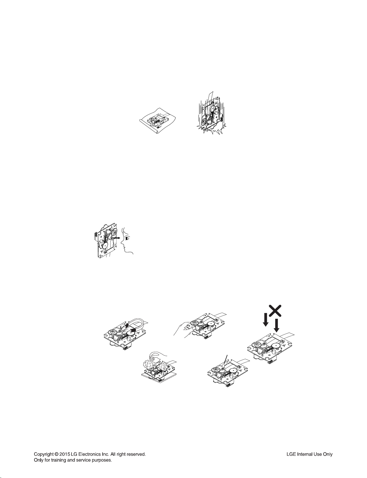
1. Notes for transport and storage
1) The pick-up should always be left in its conductive bag until immediately prior to use.
2) The pick-up should never be subjected to external pressure or impact.
Storage in conductive bag
Drop impact
2. Repair notes
1) The pick-up incorporates a strong magnet, and so should never be brought close to magnetic materials.
2) The pick-up should always be handled correctly and carefully, taking care to avoid external pressure and
impact. If it is subjected to strong pressure or impact, the result may be an operational malfunction and/or
damage to the printed-circuit board.
3) Each and every pick-up is already individually adjusted to a high degree of precision, and for that reason
the adjustment point and installation screws should absolutely never be touched.
4) Laser beams may damage the eyes!
Absolutely never permit laser beams to enter the eyes!
Also NEVER switch ON the power to the laser output part (lens, etc.) of the pick-up if it is damaged.
NEVER look directly at the laser beam, and don’t allow
contact with fingers or other exposed skin.
5) Cleaning the lens surface
If there is dust on the lens surface, the dust should be cleaned away by using an air bush (such as used
for camera lens). The lens is held by a delicate spring. When cleaning the lens surface, therefore, a cotton swab should be used, taking care not to distort lens.
Pressure
Magnet
How to hold the pick-up
Cotton swab
Conductive Sheet
6) Never attempt to disassemble the pick-up.
Spring has excess pressure. If the lens is extremely dirty, apply isopropyl alcohol to the cotton swab.
(Do not use any other liquid cleaners, because they will damage the lens.) Take care not to use too much
of this alcohol on the swab, and do not allow the alcohol to get inside the pick-up.
1-3
Pressure
Page 5
NOTES REGARDING COMPACT DISC PLAYER REPAIRS
1. Preparations
1) Compact disc players incorporate a great many ICs as well as the pick-up (laser diode). These components
are sensitive to, and easily affected by, static electricity. If such static electricity is high voltage, components
can be damaged, and for that reason components should be handled with care.
2) The pick-up is composed of many optical components and other high-precision components. Care must be
taken, therefore, to avoid repair or storage where the temperature or humidity is high, where strong magnetism is present, or where there is excessive dust.
2. Notes for repair
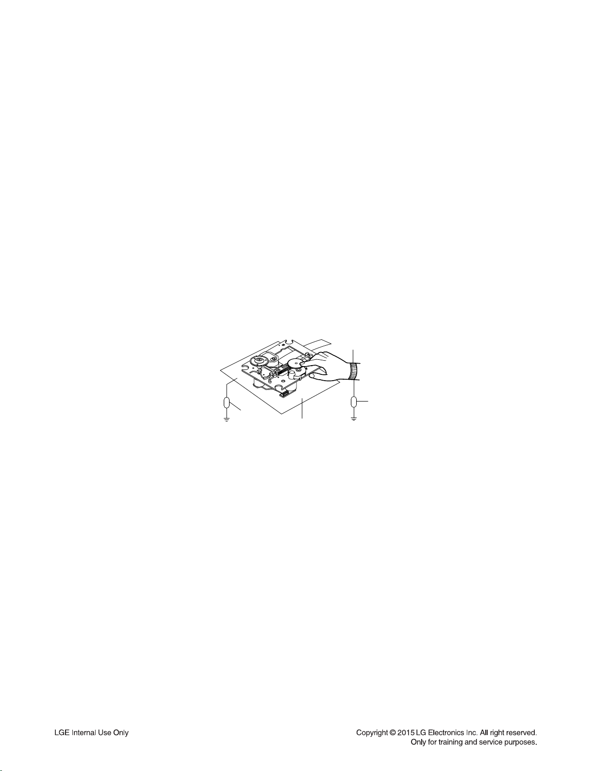
1) Before replacing a component part, first disconnect the power supply lead wire from the unit
2) All equipment, measuring instruments and tools must be grounded.
3) The workbench should be covered with a conductive sheet and grounded.
When removing the laser pick-up from its conductive bag, do not place the pick-up on the bag. (This is
because there is the possibility of damage by static electricity.)
4) To prevent AC leakage, the metal part of the soldering iron should be grounded.
5) Workers should be grounded by an armband (1 M)
6) Care should be taken not to permit the laser pick-up to come in contact with clothing, in order to prevent
static electricity changes in the clothing to escape from the armband.
7) The laser beam from the pick-up should NEVER be directly facing the eyes or bare skin.
Armband
Resistor
(1 M)
Resistor
(1 M)
Conductive
Sheet
1-4
Page 6
ESD PRECAUTIONS
Electrostatically Sensitive Devices (ESD)
Some semiconductor (solid state) devices can be damaged easily by static electricity. Such components
commonly are called Electrostatically Sensitive Devices (ESD). Examples of typical ESD devices are integrated
circuits and some field-effect transistors and semiconductor chip components. The following techniques should
be used to help reduce the incidence of component damage caused by static electricity.
1. Immediately before handling any semiconductor component or semiconductor-equipped assembly, drain off
any electrostatic charge on your body by touching a known earth ground. Alternatively, obtain and wear a
commercially available discharging wrist strap device, which should be removed for potential shock reasons
prior to applying power to the unit under test.
2. After removing an electrical assembly equipped with ESD devices, place the assembly on a conductive surface
such as aluminum foil, to prevent electrostatic charge buildup or exposure of the assembly.
3. Use only a grounded-tip soldering iron to solder or unsolder ESD devices.
4. Use only an anti-static solder removal device. Some solder removal devices not classified as "anti-static" can
generate electrical charges sufficient to damage ESD devices.
5. Do not use freon-propelled chemicals. These can generate electrical charges sufficient to damage ESD
devices.
6. Do not remove a replacement ESD device from its protective package until immediately before you are
ready to install it. (Most replacement ESD devices are packaged with leads electrically shorted together by
conductive foam, aluminum foil or comparable conductive materials).
7. Immediately before removing the protective material from the leads of a replacement ESD device, touch the
protective material to the chassis or circuit assembly into which the device will by installed.
CAUTION : BE SURE NO POWER IS APPLIED TO THE CHASSIS OR CIRCUIT, AND OBSERVE ALL OTHER
SAFETY PRECAUTIONS.
8. Minimize bodily motions when handing unpackaged replacement ESD devices. (Otherwise harmless motion
such as the brushing together of your clothes fabric or the lifting of your foot from a carpeted floor can generate
static electricity sufficient to damage an ESD device).
CAUTION. GRAPHIC SYMBOLS
THE LIGHTNING FLASH WITH APROWHEAD SYMBOL. WITHIN AN EQUILATERAL TRIANGLE, IS
INTENDED TO ALERT THE SERVICE PERSONNEL TO THE PRESENCE OF UNINSULATED
“DANGEROUS VOLTAGE” THAT MAY BE OF SUFFICIENT MAGNITUDE TO CONSTITUTE A RISK OF
ELECTRIC SHOCK.
THE EXCLAMATION POINT WITHIN AN EQUILATERAL TRIANGLE IS INTENDED TO ALERT THE
SERVICE PERSONNEL TO THE PRESENCE OF IMPORTANT SAFETY INFORMATION IN SERVICE
LITERATURE.
1-5
Page 7
HIDDEN KEY MODE
HIDDEN
MODE
Version Check POWER ON STATUS
EEPROM INITIAL POWER ON STATUS
EEPROM EDIT POWER ON STATUS
APD Test Display POWER ON STATUS
B2B, Dealer
HIDDEN MODE
Clip On/Off POWER ON STATUS
Disc Lock On/Off POWER ON STATUS
Power Disc Lock On/Off POWER ON STATUS
Demo ALL Key Lock
BT Auto Power On/Off POWER ON STATUS
Sound BYPASS POWER ON STATUS
AVAILABLE STATUS ENTRANCE KEY EXIT KEY DISPLAY
AVAILABLE STATUS ENTRANCE KEY EXIT KEY DISPLAY
POWER ON STATUS
Demo Function
Only Active
Front Play
+ RMC ‘Play’
for 5s
Front Play
+ RMC ‘|<<’
for 5s
Front Play
+ RMC ‘>>|’
for 5s
Front Play
+ RMC ‘DELETE’
for 5s
Front Play
+ RMC ‘Mute’
for 5s
Front Play
+ RMC ‘Stop’
for 5s
Front Play + RMC
‘SOUND EFFECT’
for 5s
Front Play + RMC ‘INFO’
for 5s
Front/RMC ‘Power’
for 5s
Front Play + RMC
‘PROGRAM’ for 5s
P1501290
RMC ‘PLAY’ for 1.5s
auto exit “E2P CLR”
Front Play + RMC ‘>>|’
Front Play + RMC ‘DE-
LETE’
auto exit
Front Play + RMC ‘Stop’
for 5s
Front Play + RMC
‘SOUND EFFECT’ for 5s
Front Play + RMC ‘INFO’
for 5s
Power normal Key SET
Power off
SOUND EFFECT key display ‘BYPASS’ 3s
‘LOCKED’/ ‘UNLOCKED’
‘LOCKED’/ ‘UNLOCKED’
OP0 FF
Q1501290
EQCSFFFF
OPT0-9F
( For Example )
APD MM:SS
(AUX modeH:MM:SS)
CLIP OFF
00 130 00
CLIP ON
‘KEY LOCK’/ ‘UNLOCKED’
OFF-AUTO POWER
GOOD BY Scroll
SOFTWARE UPDATE GUIDE
1) Prepare USB device without any fi les.
2) Copy software (“CM2760_FW_2015xxxxx.bin”) into this USB device.
3) Power on the unit, switch to USB function.
4) Plug in USB device which contains software, no need other operations.
5) VFD display “SEARCH” “MCS UP” “FINISH”, then unit auto power off.
1-6
Page 8

SPECIFICATIONS
• GENERAL
Power requirements Refer to the main label.
Power consumption Refer to the main label.
Networked standby : 0.5 W (If all network ports are activated.)
Dimensions (W x H x D) Approx. 170 mm x 230 mm x 276 mm
Net Weight Approx. 2.2 kg
Operating temperature 5 °C to 35 °C
Operating humidity 5 % to 90 %
• INPUTS
Portable in (PORT. IN) 0.45 Vrms (3.5 mm stereo jack) x 1
• TUNER
FM Tuning Range 87.5 to 108.0 MHz or 87.50 to 108.00 MHz
• AMPLIFIER (RMS OUTPUT POWER)
Total 160 W
Front 80 W (4 Ω at 1 kHz, 10 % THD)
• SYSTEM
Frequency response 80 to 20,000 Hz
Signal-to-noise ratio 80 dB
Dynamic range 75 dB
Bus Power Supply (USB) 5 V 500 mA
FRONT SPEAKERS
•
Type 3 Way 3 Speaker
Impedance 4 Ω
Rated Input Power 80 W
Max. Input Power 160 W
Dimensions (W x H x D) Approx. 127 mm x 295 mm x 240 mm
Net Weight Approx. 3.36 kg
• Design and specifications are subject to change without notice.
1-7
Page 9

1-8
Page 10

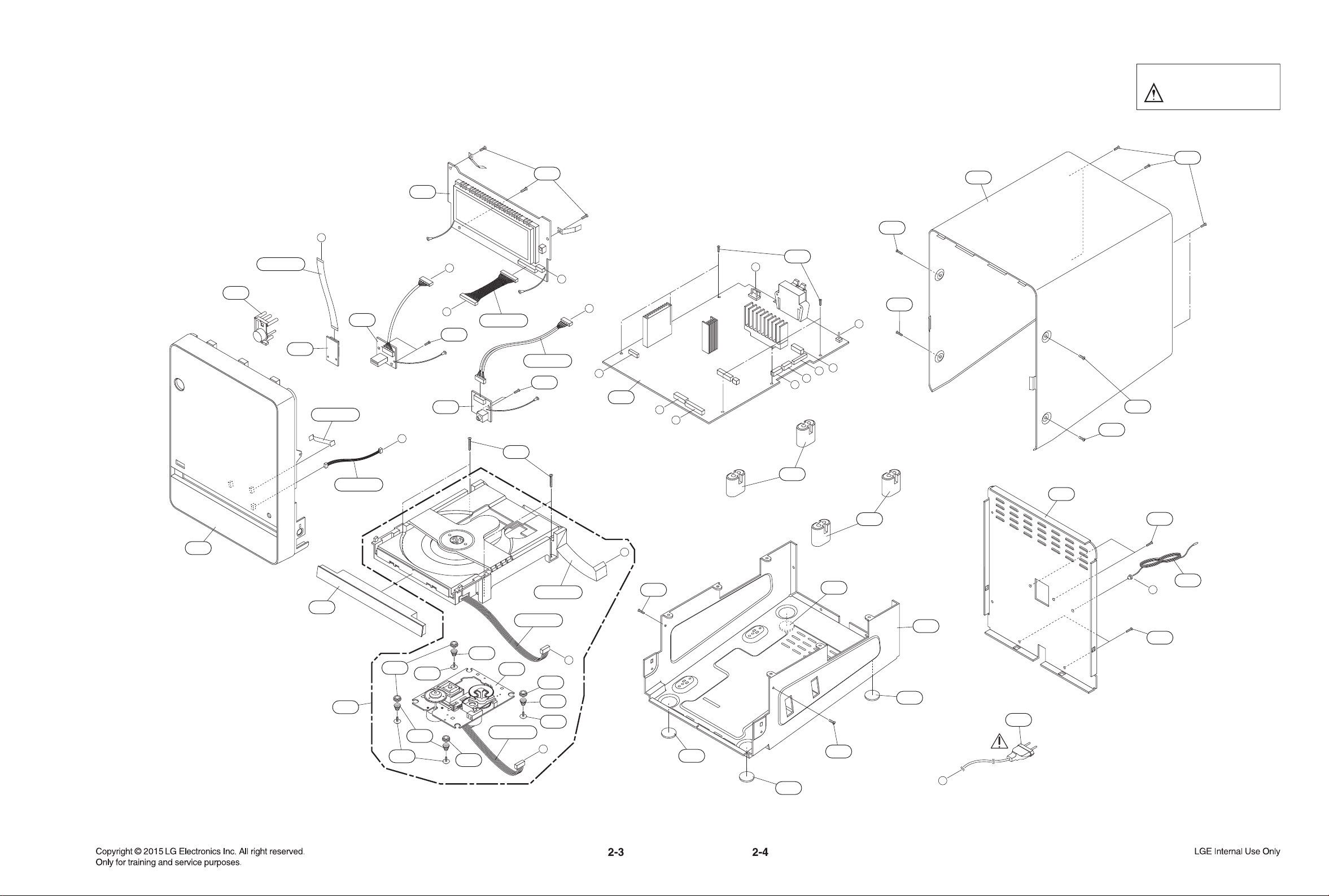
SECTION 2
CABINET & MAIN CHASSIS
CONTENTS
EXPLODED VIEWS ........................................................................................................................................... 2-3
1. CABINET AND MAIN FRAME SECTION ................................................................................................. 2-3
2. PACKING ACCESSORY SECTION ......................................................................................................... 2-7
3. SPEAKER SECTION ................................................................................................................................ 2-8
2-1
Page 11
2-2
Page 12
MAIN
VFD
BT
USB
PORTABLE
H
C
B
C
G
F
E
D
E
D
J
A
F
H
J
B
G
I
A
I
251
A52
A49
A48
A43
513
A46
266
266
516
513
265
265
515
514
513
A42
260
A00
261
261
263
A26
264
265
265
513
270
513
514
514
271
513
514
825
262
517
517
261
262
517
CABLE3
CABLE5
CABLE4
CABLE1
CABLE2
CABLE6
CABLE8
CABLE7
515
515
300
EXPLODED VIEWS
1. CABINET AND MAIN FRAME SECTION
NOTES) THE EXCLAMATION POINT WITHIN AN
EQUILATERAL TRIANGLE IS INTENDED
TO ALERT THE SERVICE PERSONNEL
TO THE PRESENCE OF IMPORTANT
SAFETY INFORMATION IN SERVICE
LITERATURE.
Page 13
Page 14
2. PACKING ACCESSORY SECTION
801 Owner’s manual
808 Batteries
803T
804 Bag
Packing
900 Remote control
803B
Packing
802 Box
Page 15
3. SPEAKER SECTION
A60L
A60R
Page 16

SECTION 3
ELECTRICAL
CONTENTS
ONE POINT REPAIR GUIDE ............................................................................................................................ 3-2
1. NO POWER PROBLEM ......................................................................................................................... 3-2
2. SPEAKER NO AUDIO OUTPUT ............................................................................................................ 3-3
3. USB NO DETECT ................................................................................................................................... 3-4
4. PROTECTION ......................................................................................................................................... 3-5
ELECTRICAL TROUBLESHOOTING GUIDE OF AUDIO PART ..................................................................... 3-8
1. SMPS POWER CIRCUIT ........................................................................................................................ 3-8
2. FLD DISPLAY CHECK ......................................................................................................................... 3-10
3. TOUCH PAD CHECK ........................................................................................................................... 3-11
4. PWM MODULATION PART .................................................................................................................. 3-12
5. POWER AMP PART CHECK ............................................................................................................... 3-13
6. AUX FUNCTION CHECK ..................................................................................................................... 3-14
7. TUNER FUNCTION CHECK................................................................................................................. 3-15
ELECTRICAL TROUBLESHOOTING GUIDE OF CD PART ......................................................................... 3-16
1. CD PART .............................................................................................................................................. 3-16
2. OPEN/ CLOSE NG ............................................................................................................................... 3-17
3. “ READING ” DISPLAY CHECK (= ONLY “CD” DISPLAY) .................................................................. 3-17
4. READING OK CHECK (= “NO DISC” DISPLAY) ................................................................................. 3-18
5. USB PART ............................................................................................................................................ 3-22
WAVEFORMS OF MAJOR CHECK POINT .................................................................................................... 3-23
WIRING DIAGRAM .......................................................................................................................................... 3-29
BLOCK DIAGRAM .......................................................................................................................................... 3-31
CIRCUIT DIAGRAMS ...................................................................................................................................... 3-33
1. MAIN - SMPS CIRCUIT DIAGRAM ...................................................................................................... 3-33
2. MAIN - CD CIRCUIT ............................................................................................................................. 3-35
3. MAIN - DSP CIRCUIT DIAGRAM ......................................................................................................... 3-37
4. MAIN - AMP/ TUNER CIRCUIT DIAGRAM .......................................................................................... 3-39
5. MAIN - POWER CIRCUIT DIAGRAM ................................................................................................... 3-41
6. TOUCH CIRCUIT DIAGRAM ................................................................................................................ 3-43
7. VFD/ USB/ PORTABLE CIRCUIT DIAGRAM ....................................................................................... 3-45
CIRCUIT VOLTAGE CHART ........................................................................................................................... 3-47
1. CONNECTORS VOLTAGE ................................................................................................................... 3-47
PRINTED CIRCUIT BOARD DIAGRAMS ....................................................................................................... 3-49
1. MAIN P. C. BOARD .............................................................................................................................. 3-49
2. TOUCH P. C. BOARD .......................................................................................................................... 3-51
3. VFD P. C. BOARD ................................................................................................................................ 3-51
4. USB P. C. BOARD ................................................................................................................................ 3-53
5. PORTABLE P. C. BOARD .................................................................................................................... 3-53
3-1
Page 17

ONE POINT REPAIR GUIDE
_
75
_
_
_
_
_
_
_
_
_
_
_
_
_
B
1
0
V
SS
3
3IO
IC200
IC202
X201
1. NO POWER PROBLEM
No power problem occurs when you power on the unit.
1-1. NO POWER
1-1-1. Solution
Replace X201, IC200, IC202.
1-1-2. How to troubleshoot (Countermeasure)
1) Check X201(Crystal).
If it does not oscillate, replace X201.
2) Check IC200(Reset IC).
If its output voltage is not more than +2.7 V, replace IC200.
3) Check IC202(DSP IC).
After Power is ON if the pin48 of IC202 is not ‘High’, replace IC202.
But, the new flash IC need to write program.
1
5
7
5
1
13
1
U
P10
U14
T14
T13
P
N1
8
9
76
82
7
81
77
7
80
AUX- DET
TOUC H-SDA
TUN- SDA
TOUC H-SCL
TUN- SCL
IR
2
1
1
T1
U
T16
U16
U
P13
P1
6
84
85
8
83
87
88
FB2 20
100
R241 330K
R228 4M7
X2 00
F
42 22p
2
C
R234 10R
R236 1M
R235
10R
X2 01
C262 33pF
32.768KHZ
GND
24M HZ
GND
V
4
0
/10
C235
220uF
C236 1
GND
104
F
GND
C243 22p
F
p
C263 33
HP-MUT E
I
PTD
D9_
D2 01
NC
DQ6
DQ5
DQ7
3
4
1
139
140
141
144
142
]
T
S
RE
R
T
CO
N
4_PD[5 ]
3_PD[6
P
1
1
D12
B
B
A13_PD[7]
D13_PGPD00
D10_
9_V D
E
C238
K
C
F-M ISO
F-S
S
SF-M OSI
SF-C S1
S
155
154
156
153
0
3
01
0
0
A
A02
P
_
B12_PGP
B11_PG
A 12_PG PA
A 11_PG PA
7
146
150
14
148
151
149
152
_PRTCK
E7_PTDO
6
D
145
3
S
0
D
TM
P
GPD02
_P
P
8
_
D7_PTCK
D
1
E1
D11_PG
D12_PGPD01
IO3V3
D2 00
NC
C201NCC202
4
Q
D
138
137
]
15_PD[ 3
A
A14_PD[4]
NC
1
Q
D
DQ2DQ3
135
136
[2 ]
D
5_P
1
B
R20 2 33R
15
DQ0
DQ
3
134
13
]
5
[1 ]
1
[
D
_PD
16_PD[ 0]
7
1
B16_P
A
A
D1 4_VDD3 3IO
E13_VS S33IO
AMP -SD- DET
AMP -OT W -DET
AMP -PDN
R20 1 10K
AZ 80 9
IC200
NC
C203
IC202
D
RST2VCC
GN
1
GND
IO3V3
IO1V2
132
131
IO3V3
3
R20 0
100R
C200
104
R
3
3
SDRAM (0 ...8)
MA2
MA0
WE#
RA201
CAS #
2
MA4
MA6
RA20
MA5
MA7
MA12
MA9
RA203
MA11
MA8
BA1
MA10
BA0
RA204
MA1
RAS #
CS#
RA205
MA3
DQM 1
DQM 0
CL K R2 04 33R
33R
33R
33R
33R
R20 6 3 3R
12
34
56
78
12
34
56
78
12
34
56
78
12
34
56
78
12
34
56
78
1-1-3. Service hint (Any picture/ Remark)
IC202
X201
IC200
< MAIN board top view >
3-2
Page 18

ONE POINT REPAIR GUIDE
IC202
Q408
Q407
2. SPEAKER NO AUDIO OUTPUT
No audio output problem occurs when you power on the unit.
2-1. NO SOUND
2-1-1. Solution
Reassemble AMP IC heat-sink, replace IC202.
2-1-2. How to troubleshoot (Countermeasure)
1) Reassemble AMP IC heat-sink (heat-sink screw must be assembled tightly).
2) Still NG, please check Q409, Q407, Q408 part out, if it is not appear 12 V.
3) If it is not appear 12 V, check IC202 pin48 output, is a high level.
4) If not high voltage, check whether IC202 damage, flash is lost.
2-1-3. Service hint (Any picture/ Remark)
Q407
Q408
< MAIN board top view >
3-3
IC202
Page 19

ONE POINT REPAIR GUIDE
IC205
3. USB NO DETECT
When USB insert, USB no detect on the unit.
3-1. NO DETECT
3-1-1. Solution
Replace IC205.
3-1-2. How to troubleshoot (Countermeasure)
1) Please check IC205.
pin1 : 5 V
2) If it is not OK, replace IC205.
3-1-3. Service hint (Any picture/ Remark)
< MAIN board top view >
3-4
IC205
Page 20

ONE POINT REPAIR GUIDE
IC300 (PWM IC)
IC301 (AMP IC)
R310, R313,
R320, R322
JK300
4. PROTECTION
4-1. D(DC) PROTECTION
4-1-1. Solution
Replace IC301(AMP IC) on MAIN board.
4-1-2. How to troubleshoot (Countermeasure)
1) Press the power button, the display is normal, no sound output. (D Protection or S Protection)
2) Check DC Voltage of speaker out Front Left channel + & -(JK300 pin2, 1), Front Right channel + & -
(JK300 pin4, 3).
3) Check resistor crack, cold solder of PWM IC out (R310, R313, R320, R322).
4) If PWM IC out is ok & speaker out(+/-) has DC Voltage, Replace IC301(AMP IC) on MAIN board.
4-1-3. Service hint (Any picture/ Remark)
JK300
R310, R313,
R320, R322
< MAIN board top view >
IC300 (PWM IC)
3-5
IC301 (AMP IC)
Page 21

ONE POINT REPAIR GUIDE
IC301 (AMP IC)
PROTECTION
4-2. S(SHUT DOWN) PROTECTION
4-2-1. Solution
Replace IC301(AMP IC) on MAIN board.
4-2-2. How to troubleshoot (Countermeasure)
1) Press the power button, the display is normal, no sound output. (D Protection or S Protection)
2) Check PVDD Voltage. (27 V)
- If PVDD abnormal Voltage, Refer to SMPS Board repair guide.
3) Check GVDD, VDD Voltage(12 V) of IC301 pin1, 22, 23, 44.
- If 12 V system abnormal Voltage, Refer to 12 V no power repair guide.
4) Check impedance (4 Ω) of speaker unit .
- If Impedance of speaker unit has 1 Ω under, replace speaker unit .
5) If check point 2, 3, 4 is ok, replace IC301(AMP IC) on MAIN board.
4-2-3. Service hint (Any picture/ Remark)
IC301 (AMP IC)
< MAIN board top view >
3-6
Page 22

ONE POINT REPAIR GUIDE
Q303
PROTECTION
4-3. B(BURNT) PROTECTION
4-3-1. Solution
Replace IC301(AMP IC) on MAIN board.
4-3-2. How to troubleshoot (Countermeasure)
1) Press the power button, the display is normal, no sound output. (B Protection)
2) Check Voltage 3.3 V of AMP_Protect signal. (collector Q303)
3) If collector Q303 is low(0 V), Replace IC301(AMP IC) on MAIN board.
4-3-3. Service hint (Any picture/ Remark)
Q303
< MAIN board top view >
3-7
Page 23

ELECTRICAL TROUBLESHOOTING GUIDE OF AUDIO PART
1. SMPS POWER CIRCUIT
No 27 V
YES
F900 normal?
YES
NTC900 normal?
YES
BD900 normal?
YES
Is the Vcc
(12 V~13 V) supplied to
IC901 pin5?
YES
The Main part IC400, IC401
is short.
NO
NO
NO
NO
Replace F900 (same fuse).
Replace NTC900.
Replace BD900.
IC901 normal?
YES
Check or replace IC901.
3-8
Page 24

ELECTRICAL TROUBLESHOOTING GUIDE OF AUDIO PART
No VCC 3.3 V
YES
Check IC400 pin4
voltage 5 V.
YES
Check D405 anode
voltage 5 V.
YES
IC401 normal?
YES
Check VCC33 network,
the device a short circuit
will cause no output.
No 12 V
NO
NO
NO
Check IC400.
Check Q401.
Replace IC401.
YES
Check Q407 collector
voltage 27 V.
YES
Check Q408 collector
voltage 15 V.
YES
Q408 normal?
YES
Check whether IC301 damage.
NO
NO
NO
Check Q407.
Check R437 ~ R441.
Check Q407, ZD400.
3-9
Page 25

ELECTRICAL TROUBLESHOOTING GUIDE OF AUDIO PART
2. FLD DISPLAY CHECK
FLD display check
Check
CN500 pin3, 11
voltage.
YES
Check VFD PCB
F+, F- both terminals:
over 3.7 V.
YES
Check power VEE:
over -33 V.
YES
Check CN500
DATA communication
pin9 STB, pin7 DATA,
pin8 CLK.
YES
NO
NO
NO
NO
Refer to
Power part troubleshooting.
Check T500, L500, Q500, Q501,
D501 part circuit.
Check T500, L500, Q500, Q501,
D501 part circuit.
IC500 pin3 STB,
pin2 DATA, pin1 CLK
Check data output.
YES
Check
pin4 --> DO --> DATA input.
YES
NO
NO
Replace the related part.
Replace the related part.
OK
YES
Check
the related part.
YES
OK
3-10
NO
Replace the related part.FLD light on?
Page 26

ELECTRICAL TROUBLESHOOTING GUIDE OF AUDIO PART
3. TOUCH PAD CHECK
Touch pad check
Check IC600 pin5
3.3 V.
YES
Check IC600
pin8:SDA,
pin9:SCL.
YES
OK
NO
NO
CN600 pin2
3.3 V.
YES
OK
Check
R652, C603, IC600
part circuit.
YES
OK
NO
NO
Refer to
Power part troubleshooting.
Replace the related part.
3-11
Page 27

ELECTRICAL TROUBLESHOOTING GUIDE OF AUDIO PART
4. PWM MODULATION PART
PWM modulation part check
IC300(TAS5538) VDD Power
Check
(pin9, 14, 35, 50).
YES
Check
IC300(TAS5538) pin11 CLK
input.
YES
Check
output IC300.
pin22: LRCK, pin: 23 CLK,
pin24: DATA.
YES
Check
IC300(TAS5538) input
pin20 -> SDA, pin21 -> SCL
pin16 -> RESET.
YES
Check
PWM modulator output
L_CH 38(-) 39(+),
R_CH 41(-) 40(+).
NO
NO
NO
NO
NO
Refer to
Power part troubleshooting.
Check IC300(TAS5538)
pin11 CLK correlation network.
Check resitance output of line
DATA: R332, CLK: R331,
LRCK: R330
Replace the related part.
Check IC300(TAS5538).
NO
NO
Replace the related part.
Replace the related part.
OK
YES
3-12
Page 28

ELECTRICAL TROUBLESHOOTING GUIDE OF AUDIO PART
5. POWER AMP PART CHECK
Power AMP part check
The Main power of 27 V.
YES
Check input power
of IC301 pin41, 40, 35, 32, 27, 26.
YES
Check
IC301 pin1, 22, 23, 44:
+12 V input.
YES
Check PWM modulator input
IC301 pin6, 8, 16, 18.
YES
Power IC301 pin28, 31, 36, 39 output.
YES
Check output
(L300, L301).
NO
NO
NO
Refer to Power part troubleshooting.
Check resistance power
IC301: R301, R335, R336, R300.
Replace the related part.
OK
YES
3-13
Page 29

ELECTRICAL TROUBLESHOOTING GUIDE OF AUDIO PART
6. AUX FUNCTION CHECK
AUX function check
Check whether
CN500 contacts or not.
YES
Check IC302
(CD4052) pin1, 12 input
waveform.
YES
Check
IC303(PCM1808) pin13, 14 input
waveform.
YES
Check IC303
pin9 SDOUT.
YES
NO
NO
NO
FB308, FB309, R348, R338,
Check
C362, C374.
YES
Check PHONE JACK
JK500, CN502.
Check IC302
pin16: 5 V.
YES
Check IC302.
Check IC303.
NO
NO
Replace the related part.
Refer to
Power part troubleshooting.
OK
3-14
Page 30

ELECTRICAL TROUBLESHOOTING GUIDE OF AUDIO PART
7. TUNER FUNCTION CHECK
Tuner function check
Check
Tuner IC304 pin11 5 V,
pin10 3.3 V.
YES
Check
IC304 pin13, 14 input
waveform.
YES
Check
IC302 pin5, 14 output
waveform.
YES
Check IC302
pin13 output.
NO
NO
NO
NO
Refer to
Power part troubleshooting
Check X300
(32.768 kHz).
YES
Check IC304.
Check IC302,
R356, C380, C384, R359.
Check IC302.
NO
NO
Replace the related part.
Refer to
SMPS troubleshooting.
OK
YES
3-15
Page 31

ELECTRICAL TROUBLESHOOTING GUIDE OF CD PART
1. CD PART
Turn on CD.
YES
Check
Open/ Close.
YES
DISC reading is OK?
YES
NO
NO
Check connector CN102.
YES
Check voltage
IC101 pin8, 19: 5 V.
YES
Check CN102
pin3: Open, pin1: Close.
Check connector
CN101, CN102, CN100.
YES
Check pick-up movement.
YES
Check IC101(AM5888).
NO
Refer to
Power part troubleshooting
If play,
audio output check.
YES
OK
NO
YES
Check IC100(BU9546).
YES
Check audio data (IC100) pin35
LRCK, pin36 BCLK, pin34 DATA.
3-16
Page 32

ELECTRICAL TROUBLESHOOTING GUIDE OF CD PART
2. OPEN/ CLOSE NG
Check connector locking.
(CN102)
YES
Check
voltage IC101(AM5888)
pin8, 19: 5 V.
YES
Check
voltage IC101(AM5888)
pin9: MOT-, pin10: MOT+.
YES
Defective mechanism.
NO
NO
Defective Main power supply.
Defective IC101.
3. “ READING ” DISPLAY CHECK (= ONLY “CD” DISPLAY)
Check connector locking.
(CN101, CN102)
YES
Check
voltage IC101(AM5888)
pin8, 19: 5 V.
NO
Defective Main power supply.
YES
Check voltage
IC200 pin2: 3.3 V.
YES
Check IC201
pin19, 17, 16, 38, 37
(CS, CAS, WE, CLK, CKE)
signal waveform.
YES
Defective IC202.
NO
NO
Defective IC200.
Check IC202.
3-17
Page 33

ELECTRICAL TROUBLESHOOTING GUIDE OF CD PART
4. READING OK CHECK (= “NO DISC” DISPLAY)
Check connector locking.
(CN100, CN101)
YES
#A
Does sled move?
YES
Does lense move?
(= Up & Down)
YES
Does laser light?
YES
Does spindle rotate?
NO
#B
NO NO
#C
NO NO
#D
NO
Check CN101
pin3, 4 (SL+, SL-).
Check CN100
pin13, 16 (F+, F-).
Check CN100
pin10 (LD).
Check CN101
pin1, 2 (SP+, SP-).
NO
NO
Defective
pick-up or IC101 or IC100.
Defective
pick-up or IC101 or IC100.
Defective
pick-up or IC101 or IC100.
Defective
pick-up or IC101 or IC100.
YES
Is reading OK?
NO
#E
Check CN100
pin14, 15 (T-, T+).
NO
Defective
pick-up or IC101 or IC100.
3-18
Page 34

ELECTRICAL TROUBLESHOOTING GUIDE OF CD PART
4-1. READING OK CHECK #A (= “NO DISC” DISPLAY)
#A
waveform appear at (IC101 pin11
Does SL+
& IC100 pin15) waveform#2
sled motor Wave.
YES
Check
CN101 line.
YES
Defective pick-up sled motor.
NO
NO
Does
SLIN waveform
appear at (IC100 pin4)
waveform #2 sled drive
wave
YES
Defective IC101.
Defective CN101.
NO
Defective IC100.
4-2. READING OK CHECK #B (= “NO DISC” DISPLAY)
#B
waveform appear at (IC101 pin14
Does F+
& IC100 pin13) waveform#3
focus coil drive wave.
YES
Check connector
CN100 line.
YES
Defective
pick-up focus actuator.
NO
NO
appear at (IC100 pin1) waveform
Does
VINFC waveform
#3 focus drive
wave.
YES
Defective IC101.
Defective CN100.
NO
Defective IC100.
3-19
Page 35

ELECTRICAL TROUBLESHOOTING GUIDE OF CD PART
4-3. READING OK CHECK #C (= “NO DISC” DISPLAY)
#C
applied to pin10 of CN100 laser
Is 3.3 V
supply voltage check.
Check connector
CN101 line.
Defective
pick-up laser part.
NO
To pin9, 30, 39, 1, 47 of IC100 RF IC
Is 3.3 V applied
supply voltage check.
YES YES
Is 2.3 V
pin9(LDO) of IC100
laser control voltage
check?
YES
Defective Q100.
NO
Defective CN101.
YES
NO
Defective IC100.
4-4. READING OK CHECK #D (= “NO DISC” DISPLAY)
#D
appear at (IC101 pin17) waveform#4
pick-up spindle motor.
Does
SPIN+ waveform
spindle motor drive
wave.
YES YES
Check connector
CN101 line.
YES
Defective
NO
NO
Does COVOUT
waveform appear at (IC100 pin16)
waveform #4 spindle drive
Wave.
Defective IC101.
Defective CN101.
NO
Defective IC100.
3-20
Page 36

ELECTRICAL TROUBLESHOOTING GUIDE OF CD PART
4-5. READING OK CHECK #E (= “NO DISC” DISPLAY)
#E
waveform appear at (IC101 pin15)
Does T+
waveform#5 tracking
coil drive wave.
YES YES
Check connector
CN100 line.
YES
Does FE, TE signal appear?
(IC100 pin61, 62, 63)
waveform #6.
NO
NO
NO
Does
appear at (IC100 pin14) waveform #5
VINTK waveform
tracking drive
wave.
Defective IC101.
Defective CN100.
Defective
pick-up or IC100.
NO
Defective IC100.
3-21
Page 37

ELECTRICAL TROUBLESHOOTING GUIDE OF CD PART
5. USB PART
Turn on USB
YES
Check
“CHECKING” or “USB”
display
YES
Check
Reading OK.
YES
OK
NO NO
NO
Check connector
(CN202 pin5, 66: 5.5 V)
YES
Check RB501
pin1: 5.5 V.
YES
Check JK501
pin5, 6: 5 V.
Check JK501
pin2 (D-), pin3 (D+).
NO
NO
Check IC205 pin1.
Check RB501 and CN202
Line connector.
Check IC202 pin62, 64.
3-22
Page 38

WAVEFORMS OF MAJOR CHECK POINT
#1. MICOM INTERFACE WAVEFORM
(IC100 pin19, 20, 30, 34) DURING
POWER ON
pin20: CD_RW
1
pin30: RESET
2
pin34: DI (IC100 pin46 DATA OUT)
3
pin19: DO (IC100 pin45 DATA IN)
4
#1. MICOM INTERFACE WAVEFORM
(IC100 pin19, 20, 30, 34) DURING
NORMAL PLAY
pin20: CD_RW
1
pin30: RESET
2
pin34: DI (IC100 pin46 DATA OUT)
3
pin19: DO (IC100 pin45 DATA IN)
4
3-23
24 1
3
Page 39

#2. SLED DRIVE AND MOTOR WAVEFORM
(IC101 pin4, 11) WHEN
FOCUS SEARCH
pin4: SLIN
5
#2. SLED DRIVE AND MOTOR WAVEFORM
(IC101 pin4, 11) DURING
NORMAL PLAY
5
pin4: SLIN
6
pin11: SL+
pin11: SL+
6
6
5
3-24
Page 40

#3. FOCUS DRIVE AND MOTOR WAVEFORM
(IC401 pin1, 14)
• WHEN FOCUS SEARCH FAILED OR
THERE IS NO DISC ON TRAY
#3. FOCUS DRIVE AND MOTOR WAVEFORM
(IC401 pin1, 14)
• THERE IS DISC ON TRAY AND FOCUS
SEARCH SUCCESS
7
pin1: VINFC
8
pin14: F+
8
7
pin1: VINFC
8
pin14: F+
7
3-25
Page 41

#4. SPINDLE DRIVE AND MOTOR WAVEFORM
(IC101 pin17, 23) WHEN TOC READING
#5. TRACK DRIVE AND MOTOR WAVEFORM
(IC101 pin16, 26) DURING
NORMAL PLAY
11
pin26: TAO
9
10
pin17: SP+
pin23: SPIN
pin16: TA+
12
12 11
10
9
3-26
Page 42

#6. RF, FOCUS AND TRACKING ERROR WAVEFORM
#7. AUDIO PART (I2S) WAVEFORM
(IC100 pin61, 62, 63)
DURING NORMAL PLAY
13
14
15
pin62: TE
pin63: RFOUT
pin61: RFMON(FE)
16
17
18
19
13 15 14
16
17 18 19
3-27
Page 43

3-28
Page 44

3-303-29
WIRING DIAGRAM
Page 45

3-323-31
SOC
USB
controller
Audio
Decoder
MLC3730
PSU
SPK OUT
L/R=80 W x 2
At THD = 10 %
L/R = 4 ohm
DC/DC LDO
EUP3484*1
SY8088*2
AZ1117*1
+27.5 V /6.8 A
BT Module
MB8811C1
Power AMP
TAS5342A
UART
SDRAM
4 M*16
Address
Data
Portable In 3.5 mm
Series Flash
32 Mbit
SPI
IIC
PWM
Processor
TAS5538
Crystal
24 MHz
Crystal
32.768 kHz
Servo
BU9546
CD
DA11
A; B; C; D; E; F
PD
LD
Motor Driver
AM5888
Load+/-
SP+/-
F+/-
SL+/-
SP; SL; Load; F
CD DI/DO
CD Busy
CD IIS
CD Reset
CD Mute
IIS
IIC
L/R PWM
L Channel
R Channel
2 CH ADC
PCM1808
AD Data
AD Clock
USB
D+/D-
0.5 A Current
Limit
TPS2041
USB Jack
VFD Driver
PT6324
VFD
BOE VFD48-
1503FN
SPI
Touch Key
AS9059
IIC
IR
Power
Key
Red
LED*26
FM IC
Si4703
FM L/R
IIC
Audio MUX
UTC4052
BLOCK DIAGRAM
Page 46

3-483-47
CIRCUIT VOLTAGE CHART
1. CONNECTORS VOLTAGE
INPUT VOLTAGE: 200-264 V / 50-60 Hz
Connector No. Pin No. Pin Name
Voltage Voltage
Spec. Stress V
Main Board
CN100
1 Vref 1.5~1.8 V 1.625 V
2 VCC 2.4~5.5 V 3.28 V
3 E 0.9~1.6 V 1.625 V
4 D 1~1.8 V 1.625 V
5 A 1~1.8 V 1.625 V
6 B 1~1.8 V 1.625 V
7 C 1~1.8 V 1.625 V
8 F 0.9~1.6 V 1.625 V
9 GND 0 V 0 V
10 LD 0~3 V 1.95 V
11 VR 0~3.3 V 1.3 V
12 MD 0~3.3 V 1.3 V
13 F+ 0~3.3 V 1.3 V
14 T- 0~3.3 V 1.3 V
15 T+ 0~3.3 V 1.3 V
16 F- 0~3.3 V 1.3 V
CN101
1 SPIND+ 1~6 V 4 V
2 SPIND- 1~5 V 4 V
3 SL+ 1~6 V 4 V
4 SL- 1~6 V 4 V
5 LIMIT SW 0~3.3 V 0~3.25 V
6 GND 0 V 0 V
CN102
1 MOT+ 3.8~5 V 4 V
2 MOT- 3.8~5 V 4 V
3 OPEN 0~3.3 V 0~3.3 V
4 GND 0 V 0 V
5 CLOSE 0~3.3 V 0 V
CN200
1 3.3V 3.3 V 3.3 V
2 GND 0 V 0 V
3 TDO 0~3.3 V 0.3 V
4 MCS-RST 0~3.3 V 3.3 V
5 TCK 0~3.3 V 3.3 V
6 TMS 0~3.3 V 3.3 V
7 TDI 0~3.3 V 3.29 V
8 NTRST 0~3.3 V 3.21 V
9 RTCK 0~3.3 V 3.3 V
CN201
1 3.3V 0~3.6 V 3.3 V
2 BT-RESET 0~3.6 V 0~3.3 V
3 RTS 0~3.6 V 0~3.3 V
4 CTS 0~3.6 V 0~3.3 V
5 TX 0~3.6 V 0~3.3 V
6 GND 0 V 0 V
7 RX 0~3.6 V 0~3.3 V
8 GND 0 V 0 V
9 SCL 0~3.6 V 0~3.3 V
10 SDA 0~3.6 V 0~3.3 V
CN202
1 GND 0 V 0 V
2 GND 0 V 0 V
3 USB+ 0~3.3 V 0.2 V
4 USB- 0~3.3 V 0 V
5 5V 0~5.5 V 5.14 V
6 5V 0~5.5 V 5.14 V
Connector No. Pin No. Pin Name
Voltage Voltage
Spec. Stress V
CN203
1 DEBUG 0~3.3 V 3.3 V
2 GND 0 V 0 V
CN300
1 GND 0 V 0 V
2 AUDIO IN 0 V 0 V
3 GND 0 V 0 V
4 AUDIO IN 0 V 0 V
5 AUDIO DETECT 0~3.3 V 0~3.25 V
CN400
1 T-SDA 0~3.6 V 3 V
2 T-SCL 0~3.6 V 3.1 V
3 3.3V 0~3.6 V 3.28 V
4 GND 0 V 0 V
5 IR 0~5 V 3.3 V
6 3.3V 0~3.6 V 3.3 V
7 VFD-SDA 0~3.6 V 3.3 V
8 VFD-SCK 0~3.6 V 3.3 V
9 VFD-CS 0~3.6 V 3.3 V
10 5V 0~6 V 4.99 V
11 GND 0 V 0 V
12 POWER-KEY 0~3.6 V 0~3.3 V
JK300
1 L- 13~14 V 13.6 V
2 L+ 13~14 V 13.6 V
3 R- 13~14 V 13.6 V
4 R+ 13~14 V 13.6 V
VFD Board
CN500
1 T-SDA 0~3.6 V 3 V
2 T-SCL 0~3.6 V 3.1 V
3 3.3V 0~3.6 V 3.28 V
4 GND 0 V 0 V
5 IR 0~5 V 3.3 V
6 3.3V 0~3.6 V 3.3 V
7 VFD-SDA 0~3.6 V 3.3 V
8 VFD-SCK 0~3.6 V 3.3 V
9 VFD-CS 0~3.6 V 3.3 V
10 5V 0~6 V 4.99 V
11 GND 0 V 0 V
12 POWER-KEY 0~3.6 V 0~3.3 V
CN503
1 T-SDA 0~3.6 V 3 V
2 T-SCL 0~3.6 V 3.1 V
3 3.3V 0~3.6 V 3.28 V
4 GND 0 V 0 V
Portable Board
CN502
1 GND 0 V 0 V
2 AUDIO IN 0 V 0 V
3 GND 0 V 0 V
4 AUDIO IN 0 V 0 V
5 AUDIO DETECT 0~3.3 V 0~3.25 V
USB Board
RB501
1 GND 0 V 0 V
2 GND 0 V 0 V
3 USB+ 0~3.3 V 0.2 V
4 USB- 0~3.3 V 0 V
5 5V 0~5.5 V 5.14 V
6 5V 0~5.5 V 5.14 V
Page 47

3-503-49
PRINTED CIRCUIT BOARD DIAGRAMS
1. MAIN P. C. BOARD
(TOP VIEW) (BOTTOM VIEW)
NOTE) Warning
Parts that are critical with respect to risk
of fire or electrical shock.
Page 48

3-523-51
2. TOUCH P. C. BOARD
3. VFD P. C. BOARD
(TOP VIEW)
(TOP VIEW)
(BOTTOM VIEW)
(BOTTOM VIEW)
Page 49

3-543-53
4. USB P. C. BOARD
5. PORTABLE P. C. BOARD
(TOP VIEW)
(TOP VIEW)
(BOTTOM VIEW)
(BOTTOM VIEW)
Page 50

3-563-55
 Loading...