

Page 1
SERVICE MANUAL
SERVICE MANUAL
CAUTION
BEFORE SERVICING THE UNIT, READ THE “SAFETY PRECAUTIONS”
IN THIS MANUAL.
Internal Use Only
FEBRUARY, 2017
MODEL: CJ87 (CJ87, CJS87F)
MODEL: CJ87
(CJ87, CJS87F)
MINI HI-FI SYSTEM
P/NO : AFN77612162
Page 2

CONTENTS
SECTION 1 ........ GENERAL
SECTION 2 ........ CABINET & MAIN CHASSIS
SECTION 3 ........ ELECTRICAL
SECTION 4 ........ MECHANISM (DM14B)
SECTION 5 ........ REPLACEMENT PARTS LIST
1-1
Page 3

SECTION 1
SUMMARY
CONTENTS
SERVICING PRECAUTIONS ............................................................................................................................ 1-3
ESD PRECAUTIONS ......................................................................................................................................... 1-5
HIDDEN KEY MODE ......................................................................................................................................... 1-6
1. HIDDEN KEY MODE TABLE .................................................................................................................... 1-6
2. HIDDEN KEY MODE DESCRIPTION ....................................................................................................... 1-7
SERVICE INFORMATION FOR EEPROM ........................................................................................................ 1-9
PROGRAM DOWNLOAD GUIDE .................................................................................................................... 1-10
FOTA UPDATE STEP USING BT APP .......................................................................................................... 1-13
SPECIFICATIONS ........................................................................................................................................... 1-15
1-2
Page 4
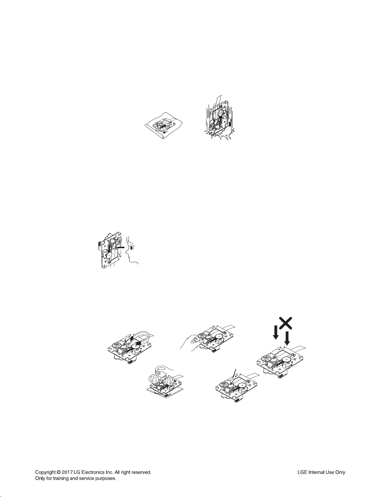
SERVICING PRECAUTIONS
NOTES REGARDING HANDLING OF THE PICK-UP
1. Notes for transport and storage
1) The pick-up should always be left in its conductive bag until immediately prior to use.
2) The pick-up should never be subjected to external pressure or impact.
Storage in conductive bag
Drop impact
2. Repair notes
1) The pick-up incorporates a strong magnet, and so should never be brought close to magnetic materials.
2) The pick-up should always be handled correctly and carefully, taking care to avoid external pressure and
impact. If it is subjected to strong pressure or impact, the result may be an operational malfunction and/or
damage to the printed-circuit board.
3) Each and every pick-up is already individually adjusted to a high degree of precision, and for that reason
the adjustment point and installation screws should absolutely never be touched.
4) Laser beams may damage the eyes!
Absolutely never permit laser beams to enter the eyes!
Also NEVER switch ON the power to the laser output part (lens, etc.) of the pick-up if it is damaged.
NEVER look directly at the laser beam, and don’t allow
contact with fingers or other exposed skin.
5) Cleaning the lens surface
If there is dust on the lens surface, the dust should be cleaned away by using an air bush (such as used
for camera lens). The lens is held by a delicate spring. When cleaning the lens surface, therefore, a cotton swab should be used, taking care not to distort lens.
Pressure
Magnet
How to hold the pick-up
Cotton swab
Conductive Sheet
6) Never attempt to disassemble the pick-up.
Spring has excess pressure. If the lens is extremely dirty, apply isopropyl alcohol to the cotton swab.
(Do not use any other liquid cleaners, because they will damage the lens.) Take care not to use too much
of this alcohol on the swab, and do not allow the alcohol to get inside the pick-up.
1-3
Pressure
Page 5
NOTES REGARDING COMPACT DISC PLAYER REPAIRS
1. Preparations
1) Compact disc players incorporate a great many ICs as well as the pick-up (laser diode). These components
are sensitive to, and easily affected by, static electricity. If such static electricity is high voltage, components
can be damaged, and for that reason components should be handled with care.
2) The pick-up is composed of many optical components and other high-precision components. Care must be
taken, therefore, to avoid repair or storage where the temperature or humidity is high, where strong magnetism is present, or where there is excessive dust.
2. Notes for repair
1) Before replacing a component part, first disconnect the power supply lead wire from the unit
2) All equipment, measuring instruments and tools must be grounded.
3) The workbench should be covered with a conductive sheet and grounded.
When removing the laser pick-up from its conductive bag, do not place the pick-up on the bag. (This is
because there is the possibility of damage by static electricity.)
4) To prevent AC leakage, the metal part of the soldering iron should be grounded.
5) Workers should be grounded by an armband (1 M)
6) Care should be taken not to permit the laser pick-up to come in contact with clothing, in order to prevent
static electricity changes in the clothing to escape from the armband.
7) The laser beam from the pick-up should NEVER be directly facing the eyes or bare skin.
Armband
Resistor
(1 M)
Resistor
(1 M)
Conductive
Sheet
1-4
Page 6
ESD PRECAUTIONS
Electrostatically Sensitive Devices (ESD)
Some semiconductor (solid state) devices can be damaged easily by static electricity. Such components
commonly are called Electrostatically Sensitive Devices (ESD). Examples of typical ESD devices are integrated
circuits and some field-effect transistors and semiconductor chip components. The following techniques should
be used to help reduce the incidence of component damage caused by static electricity.
1. Immediately before handling any semiconductor component or semiconductor-equipped assembly, drain off
any electrostatic charge on your body by touching a known earth ground. Alternatively, obtain and wear a
commercially available discharging wrist strap device, which should be removed for potential shock reasons
prior to applying power to the unit under test.
2. After removing an electrical assembly equipped with ESD devices, place the assembly on a conductive surface
such as aluminum foil, to prevent electrostatic charge buildup or exposure of the assembly.
3. Use only a grounded-tip soldering iron to solder or unsolder ESD devices.
4. Use only an anti-static solder removal device. Some solder removal devices not classified as "anti-static" can
generate electrical charges sufficient to damage ESD devices.
5. Do not use freon-propelled chemicals. These can generate electrical charges sufficient to damage ESD
devices.
6. Do not remove a replacement ESD device from its protective package until immediately before you are
ready to install it. (Most replacement ESD devices are packaged with leads electrically shorted together by
conductive foam, aluminum foil or comparable conductive materials).
7. Immediately before removing the protective material from the leads of a replacement ESD device, touch the
protective material to the chassis or circuit assembly into which the device will by installed.
CAUTION : BE SURE NO POWER IS APPLIED TO THE CHASSIS OR CIRCUIT, AND OBSERVE ALL OTHER
SAFETY PRECAUTIONS.
8. Minimize bodily motions when handing unpackaged replacement ESD devices. (Otherwise harmless motion
such as the brushing together of your clothes fabric or the lifting of your foot from a carpeted floor can generate
static electricity sufficient to damage an ESD device).
CAUTION. GRAPHIC SYMBOLS
THE LIGHTNING FLASH WITH APROWHEAD SYMBOL. WITHIN AN EQUILATERAL TRIANGLE, IS
INTENDED TO ALERT THE SERVICE PERSONNEL TO THE PRESENCE OF UNINSULATED
“DANGEROUS VOLTAGE” THAT MAY BE OF SUFFICIENT MAGNITUDE TO CONSTITUTE A RISK OF
ELECTRIC SHOCK.
THE EXCLAMATION POINT WITHIN AN EQUILATERAL TRIANGLE IS INTENDED TO ALERT THE
SERVICE PERSONNEL TO THE PRESENCE OF IMPORTANT SAFETY INFORMATION IN SERVICE
LITERATURE.
1-5
Page 7
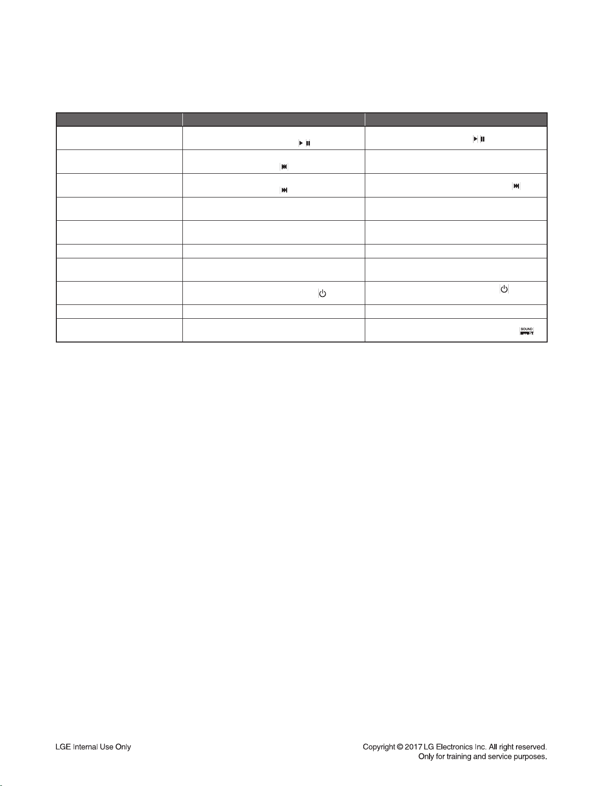
HIDDEN KEY MODE
1. HIDDEN KEY MODE TABLE
HIDDEN MODE ENTRANCE KEY(Audio) EXIT KEY
Version Check
EEPROM INITIAL
Option EDIT
APD Test Display
Disc Lock On/Off
Power Disc Lock On/Off
Demo ALL Key Lock
BT Auto Power On/Off Front/Remote Control Key ‘Power’ for 5s
ChildSafe On/Off Volume 0(Min) + Front ‘OK’ for 3s Volume 0(Min) + Front ‘OK’ for 3s
Measure
Front ‘Stop’
+ Remote Control Key ‘Play’ for 5s
Front ‘Stop’
+ Remote Control Key ‘ ‘ for 5s
Front ‘Stop’
+ Remote Control Key ‘ ‘ for 5s
Front ‘Stop’
+ Remote Control Key ‘3’ for 5s
Front ‘Stop’ +
Remote Control Key ‘Stop’ for 5s
Front ‘Stop’ + Front ‘Open’ for 5s Front ‘Stop’ + Front ‘Open’ for 5s
Front ‘Stop’
+ Remote Control Key ‘9’ for 5s
Front ‘Stop’
+ Remote Control Key ‘1’ for 5s
/
Remote Control Key ‘Play’ for 1.5s
Auto exit
Front ‘Stop’ + Remote Control Key ‘ ‘
Auto exit
Front ‘Stop’
+ Remote Control Key ‘Stop’ for 5s
Front ‘Stop’
+ Remote Control Key ‘9’ for 5s
Front/Remote Control Key ‘Power’
SET Power Off
Remote Control Key ‘SOUND EFFECT’
/
1-6
Page 8
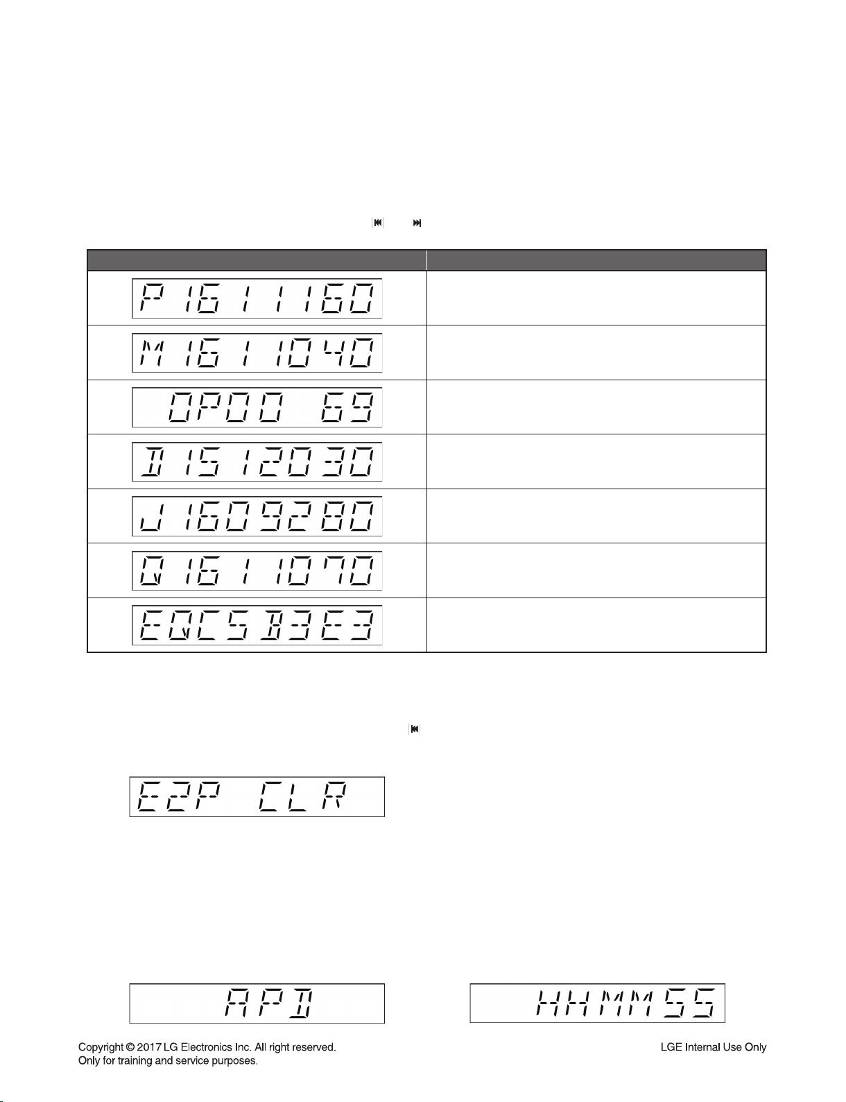
2. HIDDEN KEY MODE DESCRIPTION
2-1. Version Check
- Function : Version Check.
- Entrance Key : Front ‘Stop’ + Remote Control Key ‘Play’ for 5s.
- Exit Key : Remote Control Key ‘Play’ for 1.5s.
- Operation explanation : Remote Control Key OR .
VFD Display (Example) Result
MCS Version
MICOM Version
OPTION Version
DEMO Version
DJ PRO Version
EQ Version
EQ Check sum Version
2-2. EEPROM Initial
- Function : Initialize data stored in EEPROM and BACKUP RAM data.
- Entrance Key : Front ‘Stop’ + Remote Control Key ‘ ‘ for 5s.
- Exit Key : Auto exit.
- Explanation : ‘E2P CLR’ is displayed on the VPD and turn off the power automatically.
2-3. OPTION EDIT (EEPROM)
- Refer to the page 00.
2-4. APD Test Display
- Function : Auto Power Down timer is displayed on VFD.
- Entrance Key : Front ‘Stop’ + Remote Control Key ‘3’ for 5s.
- Exit Key : Auto Exit.
- Explanation : display APD Timer HH=(hour) MM=(min), SS=(sec).
1-7
Page 9
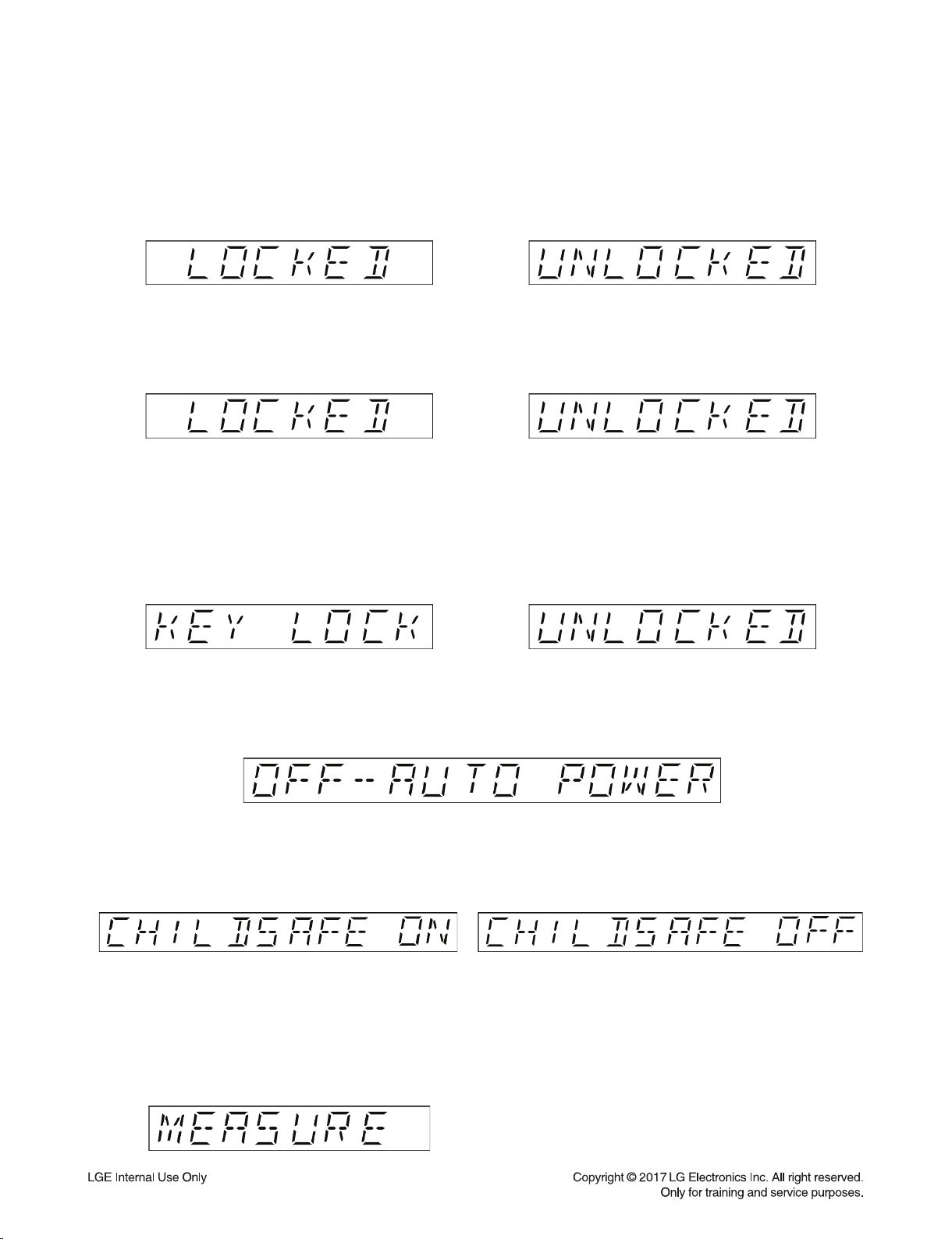
2-5. Disc Lock On/Off
- Function : Lock Open Key.
- Entrance Key : Front ‘Stop’ + Remote Control Key ‘Stop’ for 5s.
- Exit Key : Front ‘Stop’ + Remote Control Key ‘Stop’ for 5s.
- Operation Explain : Open Key Block ‘LOCKED’.
2-6. Power Disc Lock On/Off
- Function : Lock Power / Open / Front Volume Key.
- Entrance Key : Front ‘Stop’ + Front ‘Open’ for 5s.
- Exit Key : Front ‘Stop’ + Front ‘Open’ for 5s.
2-7. Demo All Key Lock
- Function : All key is blocked on Demo Mode.
- Entrance Key : Front ‘Stop’ + Remote Control Key ‘9’ for 5s.
- Exit Key : Front ‘Stop’ + Remote Control Key ‘9’ for 5s.
- Operation Key : In demo mode, all key blocks.
(only the volume key is effective when All Key Lock is enabled.)
To release Demo Mode, it is available after All Key Lock Off.
2-8. BT Auto Power On/Off
- Function : Ability to disable BT Auto Power On function by network shutdown regulation.
- Entrance Key : Front/Remote Control Key ‘Power’ for 5s.
- Exit Key : SET Power Off with Front / Remote Control Key ‘Power’.
2-9. ChildSafe On/Off
- Function : Power off Fade-in to previous volume.
- Entrance Key : Volume 0(Min) + Front ‘OK’ for 3s.
- Exit Key : Volume 0(Min) + Front ‘OK’ for 3s.
2-10. Measure
- Function : Change to EQ for Measure mode,
Down algorithm operation Disable,
Change to output setting value for measure mode.
- Entrance Key : Front ‘Stop’ + Remote Control Key ‘1’ for 5s
- Exit Key : Remote Control Key ‘SOUND EFFECT’
1-8
Page 10
SERVICE INFORMATION FOR EEPROM
POWER ON
VFD “NO DISC” status
It is possible at any function.
(ex. It is possible at VFD “NO USB” status, too.)
This is an example.
Front ‘Stop’ + Remote control ‘ ’
push same timing during 5 s
FLD “OP00-…..”
Move to appropriate position
And make changes with remote control
“ , , , REPEAT” key.
/
Press ‘Stop’ Key
VFD “WRITE OK”
DETECT NEW EEPROM
(OPTION EDIT SCREEN)
NAME
OPT0
OPT1
OPT2
OPT3
OPT4
OPT5
OPT6
OPT7
OPT8
OPT9
OPT10
OPT11
OPT12
OPT13
OPT14
HEX
01
31
2D
26
19
00
00
43
4A
38
37
00
00
00
00
Front ‘Stop’ + Remote control ‘ ’
push same timing during 5 s
VFD “E2P CLR”
Completed
1-9
Page 11

PROGRAM DOWNLOAD GUIDE
1. AUDIO PROGRAM
Download program file name must be MICOM_CJ87_YYMMDDX.HEX
If security program(Water Wall) is activated on PC, you must save the file to the USB storage device
and disable the security software, then download the file to your set.
Downloading file proceeds in the same way at USB1 function and USB2 function.
Caution:
When downloading the file, you should neither unplug the USB device, change to the other function,
nor power off the device. USB device must be unplugged when the downloading process is completed.
ON VFD DISPLAY SCREEN
NO USB
Insert USB device at USB function.
SEARCH
MICOM UP
FINISH
AUTO POWER OFF
1) (Fast) Format USB device.
2) Copy Firmware file to USB device.
1-10
Page 12
2. CD PROGRAM
Download program file name must be HG790_CJ87_YYMMDDX.bin
If security program(Water Wall) is activated on PC, you must save the file to the USB storage device
and disable the security software, then download the file to your set.
Downloading file proceeds in the same way at USB1 function and USB2 function.
Caution:
When downloading the file, you should neither unplug the USB device, change to the other function,
nor power off the device. USB device must be unplugged when the downloading process is completed.
ON VFD DISPLAY SCREEN
NO USB
Insert USB device at USB function.
SEARCH
FIRMWARE
FINISH
AUTO POWER OFF
1) (Fast) Format USB device.
2) Copy Firmware file to USB device.
1-11
Page 13
3. EQ & DEMO PROGRAM
Download program file name must be EQ_DEMO_PRG_CJ87_XXXX.BIN
If security program(Water Wall) is activated on PC, you must save the file to the USB storage device
and disable the security software, then download the file to your set.
Downloading file proceeds in the same way at USB1 function and USB2 function.
Caution:
When downloading the file, you should neither unplug the USB device, change to the other function,
nor power off the device. USB device must be unplugged when the downloading process is completed.
ON VFD DISPLAY SCREEN
NO USB
Insert USB device at USB function.
SEARCH
EQDEMOUP
FINISH
AUTO POWER OFF
1) (Fast) Format USB device.
2) Copy Firmware file to USB device.
1-12
Page 14
FOTA UPDATE STEP USING BT APP
Step1 : App connecting
(Check FW version)
After connecting the BT App with SET,
the user could fi nd the “Device Version info” on
Setting tab.
Step2 : Device version info
When touch the “Device Version info” button,
user could fi nd the current and latest SET
version on pop-up menu.
Step3 : Select update button
When touch the “Update” button, user could
update the SET fi rmware using FOTA.
Step4 : Confi rm update
Select the OK button on the caution message.
1-13
Page 15
Step5 : Download from CDN server
Step6 : Transfer FW
1st step is download from CDN server to
smart phone. The progress bar is displayed
on BT App.
After completed the download from server,
smart phone start to transfer the fi rmware to the
SET. The progress bar is displayed on BT App.
Step7 : FW Flash Writing Step8 : FOTA complete
After completed the download from the smart
phone, the SET overwrite the fi rmware to fl ash
memory.
When fi nishing the fl ash memory writing, pop-up
message about fi nish is displayed and the SET
auto power off.
1-14
Page 16

SPECIFICATIONS
GENERAL
Power requirements Refer to the main label on the unit.
Power consumption Refer to the main label on the unit.
Networked standby : 0.5 W
(If all network ports are activated.)
Dimensions (W x H x D) Approx. 450 mm x 170 mm x 349 mm
Operating temperature 5 °C to 35 °C (41 °F to 95 °F)
Operating humidity 60 %
INPUTS
Analog audio in (AUX IN) 2.0 Vrms (1 kHz, 0 dB), 600 Ω, RCA jack (L, R)
Portable in (PORT. IN) 1.0 Vrms (3.5 mm stereo jack) x 1
Microphone (MIC 1/2) Sensitivity 20 mV (1 kHz), 6.3 mm jack x 2
TUNER
FM Tuning Range 87.5 to 108.0 MHz or 87.50 to 108.00 MHz
AM Tuning Range 522 to 1,620 kHz, 520 to 1,710 kHz or 522 to 1,710 kHz
SYSTEM
Frequency Response 40 to 20,000 Hz
Signal-to-noise ratio More than 75 dB
Dynamic range More than 80 dB
Bus Power Supply (USB) 5 V 500 mA
AMPLIFIER (RMS Output power)
Total output 2,350 W RMS
HIGH 585 W RMS x 2 (6 Ω at 5 kHz, 30 % THD)
LOW 590 W RMS x 2 (6 Ω at 1 kHz, 30 % THD)
FRONT SPEAKER
Type HIGH : 1 Way 1 Speaker
LOW : 1 Way 1 Speaker
Impedance HIGH : 6 Ω
LOW : 6 Ω
Rated Input power HIGH : 585 W RMS
LOW : 590 W RMS
Max. Input power HIGH : 1,170 W RMS
LOW : 1,180 W RMS
Dimensions (W x H x D) Approx. 320 mm x 454 mm x 309 mm
Design and specifications are subject to change without notice.
1-15
Page 17
1-16
Page 18

SECTION 2
CABINET & MAIN CHASSIS
CONTENTS
EXPLODED VIEWS ......................................................................................................................................... 2-3
1. CABINET AND MAIN FRAME SECTION ................................................................................................. 2-3
2. PACKING ACCESSORY SECTION ......................................................................................................... 2-7
3. SPEAKER SECTION ................................................................................................................................ 2-8
DISASSEMBLY INSTRUCTIONS ................................................................................................................... 2-9
1. Case Top ................................................................................................................................................... 2-9
2. Panel Front Assembly ............................................................................................................................... 2-9
3. Panel PCB & Multi Knob ......................................................................................................................... 2-10
4. Bracket Hook ........................................................................................................................................... 2-11
5. Main PCB & SMPS PCB ......................................................................................................................... 2-12
6. Bracket Inner ........................................................................................................................................... 2-13
7. MD & Lighting PCB ................................................................................................................................. 2-14
8. Panel Rear .............................................................................................................................................. 2-14
2-1
Page 19

2-2
Page 20
F
D
E
A
C
B
A
H
D
E
B
H
G
K
SMPS
MIC
J
A47
262
A45
498
498
271
498
271
271
271
BT
CABLE1
443
265
265
252
252
A42
270
443
443
443
443
MAIN
272
K
300
498
A52
443
275
443
273
G
L
F
CABLE2
A46
254
254
443
C
L
FRONT
A43
266
443
J
263
443
274
443
EXPLODED VIEWS
1. CABINET AND MAIN FRAME SECTION
2-42-3
NOTES) THE EXCLAMATION POINT WITHIN AN
EQUILATERAL TRIANGLE IS INTENDED
TO ALERT THE SERVICE PERSONNEL
TO THE PRESENCE OF IMPORTANT
SAFETY INFORMATION IN SERVICE
LITERATURE.
Page 21
2-62-5
Page 22
2. PACKING ACCESSORY SECTION
801 Owner’s manual
825 FM antenna
808 Battries
900 Remote control
Packing803
804 Bag
802 Box
2-7
Page 23
3. SPEAKER SECTION
• FRONT SPEAKER
A60
2-8
Page 24
DISASSEMBLY INSTRUCTIONS
1. Case Top
1-1) Remove the 7 Screws.
1-2) Remove the Case Top.
Figure 1
2. Panel Front Assembly
2-1) Disconnect the 4 FFC Cables from the Main Board.
2-2) Unhook the 10 Locking Tabs by using Flat-head screwdriver.
2-3) Remove the Panel Front Assembly.
Figure 2
2-9
Page 25
(H1)
3. Panel PCB & Multi Knob
3-1) Multi Knob
3-1-1) Insert a Flat-head screwdriver in the hole (H1).
3-1-2) Remove the Multi Knob.
3-2) Jack PCB
3-2-1) Remove the 2 Screws.
3-2-2) Remove the Jack PCB.
3-3) BT Module
3-3-1) Unhook the Locking tab (L1).
3-3-2) Remove the BT Module.
3-4) Front PCB
3-4-1) Remove the 11 Screws.
3-4-2) Remove the Front PCB.
(L1)
(H1)
(H1)
2
(L2)
(L2)
1
2
(H1)
Figure 3
2-10
Page 26
4. Bracket Hook
4-1) Remove the 2 Screws.
4-2) Rotate 90 degrees to the front.
4-3) Remove the Bracket Hook.
Figure 4
2-11
Page 27

5. Main PCB & SMPS PCB
5-1) Remove the 2 Screws from the Panel Rear.
5-2) Disconnect the 4 FFC Cables from the Main Board.
5-3) Remove the 10 Screws from the Main Board & SMPS Board.
5-4) Remove the Main Board & SMPS Board.
Figure 5
2-12
Page 28

6. Bracket Inner
6-1) Remove the 2 Screws from the Panel Rear.
6-2) Remove the 2 Screws from the Bracket Inner.
6-3) Remove the Bracket Inner.
Figure 6
2-13
Page 29

7. MD & Lighting PCB
7-1) Remove the 2 Screws from the MD.
7-2) Remove the 2 Screws from the Lighting PCB.
7-3) Remove the MD & Lighting PCB.
8. Panel Rear
8-1) Remove the 1 Screw from the Panel Rear.
8-2) Remove the Panel Rear.
Figure 7
Figure 8
2-14
Page 30

SECTION 3
ELECTRICAL
CONTENTS
ONE POINT REPAIR GUIDE ............................................................................................................................ 3-2
1. NO POWER ............................................................................................................................................ 3-2
2. NO BOOTING WHEN POWER ON THE SET........................................................................................ 3-4
3. NO BOOTING IN CD/USB FUNCTION .................................................................................................. 3-5
4. NO OPERATION OF MD ...................................................................................................................... 3-10
5. NO SOUND IN THE USB FUNCTION .................................................................................................. 3-15
6. AUDIO OUTPUT IS SMALL OR NO AUDIO OUTPUT ........................................................................ 3-16
7. NO POWER ON (STANDBY LED IS BLINKING) ................................................................................. 3-17
8. SPEAKER NO AUDIO .......................................................................................................................... 3-18
9. NO SOUND ........................................................................................................................................... 3-19
10. VFD IS NOT DISPLAYED WHEN POWER ON THE SET ................................................................... 3-24
ELECTRICAL TROUBLESHOOTING GUIDE ................................................................................................. 3-25
1. POWER SUPPLY ON SMPS BOARD .................................................................................................. 3-25
2. SYSTEM PART ..................................................................................................................................... 3-28
3. NO AUDIO CHECK ............................................................................................................................... 3-29
WAVEFORMS OF MAJOR CHECK POINT .................................................................................................... 3-34
1. DSP (IC501) .......................................................................................................................................... 3-34
2. PWM (IC600) ........................................................................................................................................ 3-35
3. SERVO (IC401) ..................................................................................................................................... 3-36
4. MOTOR DRIVER (IC400) ..................................................................................................................... 3-37
5. ADC ....................................................................................................................................................... 3-38
6. USB ....................................................................................................................................................... 3-38
7. BLUETOOTH ........................................................................................................................................ 3-39
WIRING DIAGRAM .......................................................................................................................................... 3-41
BLOCK DIAGRAM .......................................................................................................................................... 3-43
CIRCUIT VOLTAGE CHART ........................................................................................................................... 3-45
1. CAPACITOR VOLTAGE ....................................................................................................................... 3-45
PRINTED CIRCUIT BOARD DIAGRAMS ....................................................................................................... 3-47
1. SMPS P.C.BOARD DIAGRAM ............................................................................................................. 3-47
2. MAIN P.C.BOARD DIAGRAM .............................................................................................................. 3-51
3. FRONT P.C.BOARD DIAGRAM ........................................................................................................... 3-55
4. JACK P.C.BOARD DIAGRAM .............................................................................................................. 3-59
3-1
Page 31

ONE POINT REPAIR GUIDE
1. NO POWER
If the unit doesn’t work by no power problem, repair the set according to the following guide.
1-1. POWER
1-1-1. Solution
Please check and replace F901, BD901 and TH900 ~ TH903 on SMPS board.
1-1-2. How to troubleshoot (Countermeasure)
1) Check if the fuse F901 is open or short-circuit.
2) Check if the bridge diode BD901 is short-circuit by over current with a digital multi meter.
3) Check if the NTC thermistor TH900 ~ TH903 is normal or open.
1-1-3. Service hint (Any picture/ Remark)
< F901 >
If F901 is not short-circuit,
replace it with a same
specifi cations one.
< BD901 >
If BD901 is short-circuit,
replace it with a new one.
3-2
<TH900 ~ TH903 >
If TH900 ~ TH903 is open,
replace it with a new one.
Page 32

ONE POINT REPAIR GUIDE
NO POWER
If the unit doesn’t work by no ±PVDD problem, repair the set according to the following guide.
1-2. AMP POWER
1-2-1. Solution
Please check and replace F911, Q905, Q906 on SMPS board.
1-2-2. How to troubleshoot (Countermeasure)
1) Check if the fuse F911 is open or short-circuit.
2) Check the Drain-Source or Drain-Gate, Gate-Source Resistance of Q905, Q906 with a digital multimeter.
If it is short condition, it’s destroyed. Replace it with a new one.
(Please replace 2 FET at the same time although several FET is OK).
1-2-3. Service hint (Any picture/ Remark)
< F911 >
If F911 is not short-circuit,
replace it with a same specifi cations one.
< Q905, Q906 >
If Q905, Q906 is short-circuit,
replace it with a new one.
3-3
Page 33

ONE POINT REPAIR GUIDE
X500
(24 MHz)
X501
(32.768 kHz)
KEY1
(R53D)
PWR_CTRL
(R508)
IC501
2. NO BOOTING WHEN POWER ON THE SET
The set doesn’t work when press the power button on the FRONT board or the remote control.
2-1. IC501
2-1-1. Solution
Replace IC501 on MAIN board.
2-1-2. How to troubleshoot (Countermeasure)
1) Check the 5.6 VA(CN300) and DVCC 3.3 V(IC306) in standby mode.
If there is no 5.6 VA, check the SMPS and if doesn’t appear 3.3 V, check IC306.
2) Check 5.6 VA, +12 V, F+, F-, an VH when power on the set.
If the set doesn’t work regardless of what the KEY1 changes high to low while pressing the power button.
X500 and X501 work normally but, if you can not power on the set, replace the IC501 with a new one
on the main board.
2-1-3. Service hint (Any picture/ Remark)
KEY1
(R53D)
PWR_CTRL
(R508)
< MAIN board top view >
3-4
IC501
X501
(32.768 kHz)
X500
(24 MHz)
Page 34

ONE POINT REPAIR GUIDE
IC302
IC306
3. NO BOOTING IN CD/USB FUNCTION
After you turn on power key and displayed message in the following order (HELLO VOL XX CD
or USB) on VFD, it will not display other message on VFD, and it will not boot-up normally.
3-1. NO VCC33, VCC12
3-1-1. Solution
Please check and replace IC302, IC306 on MAIN board.
3-1-2. How to troubleshoot (Countermeasure)
1) Check voltage of IC306 pin5 & IC301 pin4 on MAIN board.
If IC306 pin5(about 3.4 V) doesn’t come out, check 3.4 VA from IC301.
If IC301 pin4(about 4.9 V) doesn’t come out, check +5.1 VA from SMPS.
2) If IC306 pin3(about 3.4 V) is normal, check the PWR_CTRL(IC306 pin4) is high(about 3.3 V)
If PWR_CTRL isn’t high, check pin D11 of IC501 & R550.
3) If PWR_CTRL is high, check R550 and if there’s no defective component then replace IC306.
4) If 3.3 V(VCC33) is normal, check 1.2 V output(pin3) voltage of IC302.
If 1.2 V of IC302 pin3 doesn’t come out, then replace IC302.
3-1-3. Service hint (Any picture/ Remark)
IC306
< MAIN board top view >
IC302
3-5
Page 35

ONE POINT REPAIR GUIDE
O
IC501
X500
NO BOOTING IN CD/USB FUNCTION
After you turn on power key and displayed message in the following order (HELLO VOL XX CD
or USB) on VFD, it will not display other message on VFD, and it will not boot-up normally.
3-2. CRYSTAL (X500)
3-2-1. Solution
Replace X500 on MAIN board.
3-2-2. How to troubleshoot (Countermeasure)
1) If 3.3 V & 1.2 V is normal, check reset ‘HIGH’ of IC501 pin T12 on MAIN board.
If MAIN_RESET isn’t HIGH, check MICOM(IC100) pin40.
2) If MAIN_RESET is HIGH, check the soldering status of 24 MHz crystal(X500).
3) If the crystal(X500) doesn’t oscillate, check R551, R55E, C536, C53B around crystal(X500)
If there’s no defective component, then replace X500.
3-2-3. Service hint (Any picture/ Remark)
XXXII
IC501
X500
XXO
< MAIN board top view >
< Signal waveform >
X500
3-6
Page 36

ONE POINT REPAIR GUIDE
VCC
CLK
DO
CS#
IC503
NO BOOTING IN CD/USB FUNCTION
After you turn on power key and displayed message in the following order (HELLO VOL XX CD
or USB) on VFD, it will not display other message on VFD, and it will not boot-up normally.
3-3. SERIAL FLASH (IC503)
3-3-1. Solution
Please check and replace IC503 on MAIN board.
3-3-2. How to troubleshoot (Countermeasure)
1) If the crystal(X500) does oscillate, check Serial Flash(IC503) on MAIN board.
Check pin8(VCC), pin6(CLK), pin1(CS), pin2(DO), pin5(DI) of below waveform.
2) If pin1, 2, 5, 6, 8 doesn’t come out, check damping resistor(R54A, R54B, R54C, R54D) of IC503.
If damping resistor of IC503 is OK, then replace IC503. (it need to download program)
3) After change IC503, if It is still not below waveform, check IC501(DSP IC).
3-3-3. Service hint (Any picture/ Remark)
V
IC503
< MAIN board bottom view >
< Signal waveform >
3-7
Page 37

ONE POINT REPAIR GUIDE
V CC
Res et
Add ress
Data
/ CS
R AS
/ WE
CAS
IC504
NO BOOTING IN CD/USB FUNCTION
After you turn on power key and displayed message in the following order (HELLO VOL XX CD
or USB) on VFD, it will not display other message on VFD, and it will not boot-up normally.
3-4. SDRAM (IC504)
3-4-1. Solution
Please check and replace IC504 on MAIN board.
3-4-2. How to troubleshoot (Countermeasure)
1) Check below waveform & soldering status of SDRAM(IC504) on MAIN board.
If pin17(#CAS), pin18(#RAS), pin19(#CS), pin38(CLK), pin29(address), pin2(DQ) doesn’t come out,
check damping resistor(R565, R567, R569, R563).
2) If resistor is OK, then replace IC502(SDRAM).
3) After change IC504, if It is still not below waveform, check IC501(DSP IC).
3-4-3. Service hint (Any picture/ Remark)
V
IC504
/
< Signal waveform >< MAIN board bottom view >
3-8
Page 38

ONE POINT REPAIR GUIDE
IC501
NO BOOTING IN CD/USB FUNCTION
After you turn on power key and displayed message in the following order (HELLO VOL XX CD
or USB) on VFD, it will not display other message on VFD, and it will not boot-up normally.
3-5. DSP (IC501)
3-5-1. Solution
Please check and replace IC501 on MAIN board.
3-5-2. How to troubleshoot (Countermeasure)
1) After check them by previous pages about no booting, if the set is still no booting,
Check soldering status of IC501.
2) If below bootstrap waveform doesn’t come out, then replace IC501(DSP IC).
3-5-3. Service hint (Any picture/ Remark)
R578
PGPB07
(YELLOW)
R598
PAD19
IC501
(GREEN)
< MAIN board top view >
R597
PAD20
(PINK)
< Bootstrap waveform >
3-9
Page 39

ONE POINT REPAIR GUIDE
SP-
pin8 of CN401
SP+
pin6 of CN401
IC400
4. NO OPERATION OF MD
When no sound output in the CD function, you can not listen to music reading data from a CD disc
if the servo motors in MD don’t work. This step is for checking the spindle motor among them.
4-1. SPINDLE MOTOR
4-1-1. Solution
Replace IC401 or IC400 on MAIN board.
4-1-2. How to troubleshoot (Countermeasure)
1) Check the SPDO signal from pin16 of IC401.
If no signal, check 3.3 V(RF) and X400.
2) Check the SP- & SP+ from IC400 to CN401 for driving SPINDLE motor. It is about 3.6 Vp-p.
If no signal, check +1.8 V and DVCC +5 V for IC400.
3) Check if the FFC cable is solidly connected between CN401 and MD.
4) Check the MD.
If the spindle motor is short-circuit or has any trouble, it can not rotate CD discs.
Please check the function after changing another MD.
4-1-3. Service hint (Any picture/ Remark)
SP-
pin8 of CN401
pin6 of CN401
SP+
zwR
zwT
< Waveform of SP- & SP+
for driving SPINDLE motor >
IC400
< MAIN board top view >
3-10
Page 40

SL-
pin9 of CN401
SL+
pin7 of CN401
IC400
ONE POINT REPAIR GUIDE
NO OPERATION OF MD
When no sound output in the CD function, you can not listen to music reading data from a CD disc
if the servo motors in MD don’t work. This step is for checking the sled motor among them.
4-2. SLED MOTOR
4-2-1. Solution
Replace IC401 or IC400 on MAIN board.
4-2-2. How to troubleshoot (Countermeasure)
1) Check the SLDO signal from pin23 of IC401.
If no signal, check 3.3 V (RF) and X400.
2) Check the SLED+ & SLED- from IC400 to CN401 for driving SPINDLE motor. It is about 2.9 Vp-p.
If no signal, check +1.8 V and +5 V for IC400.
3) Check if the FFC cable is solidly connected between CN401 and MD.
4) Check the MD.
If the sled motor is sort-circuit or has any trouble, it can not move the pickup module.
Please check the function after changing another MD.
4-2-3. Service hint (Any picture/ Remark)
SL+
zsR
SL-
pin9 of CN401
pin7 of CN401
zsT
< Waveform of SL- & SL+
for driving SLED motor >
IC400
< MAIN board top view >
3-11
Page 41

ONE POINT REPAIR GUIDE
LO+
pin4 of CN401
LO-
pin2 of CN401
MOT_CLOSE
pin6 of IC400
MOT_OPEN
pin7 of IC400
NO OPERATION OF MD
When no sound output in the CD function, you can not listen to music reading data from a CD disc
if the servo motors in MD don’t work. This step is for checking the tray open/close motor among them.
4-3. TRAY OPEN/ CLOSE MOTOR
4-3-1. Solution
Replace IC401 or IC400 on MAIN board.
4-3-2. How to troubleshoot (Countermeasure)
1) Check MOT_OPEN & MOT_CLOSE signals from pin K4 & L4 of IC501 to IC400.
If no signal, check +1.8 V & + 5 V to IC400.
2) Check LOAD ± from IC400 to CN401 for driving the tray open/ close motor. It is about 3.85 Vp-p.
If no signal, check +5 V to IC401. If it has any trouble, replace it with a new one.
3) Check if the FFC cable is solidly connected between CN401 and MD.
4) Check the MD.
If the tray motor is short-circuit or has any trouble, it can not open or close the tray.
Please check the function after changing another MD.
4-3-3. Service hint (Any picture/ Remark)
svT
svROylkP
LO+
pin4 of CN401
pin2 of CN401
LO-
MOT_OPEN
pin7 of IC400
tv{ v w lu
tv{ jsvz l
< Waveform
for driving tray open/ close motor >
MOT_CLOSE
pin6 of IC400
< MAIN board top view >
3-12
Page 42

ONE POINT REPAIR GUIDE
TR-
pin17 of CN400
TR+
pin16 of CN400
NO OPERATION OF MD
When no sound output in the CD function, you can not listen to music reading data from a CD disc
if the pickup module in MD doesn’t work. This step is for checking the laser tracking actuator.
4-4. LASER TRACKING ACTUATOR
4-4-1. Solution
Replace IC401 or IC400 on MAIN board.
4-4-2. How to troubleshoot (Countermeasure)
The tracking actuator makes the laser beam be positioned in the center of a track on CD disc.
1) Check the TRD signal from pin14 of IC401.
If no signal, check 3.3 V(RF) and X400.
2) Check TR- & TR+ from IC400 to CN400 for driving the tracking actuator.
If no signal, check +1.8 V and +5 V for IC400.
3) Check if the FFC cable is solidly connected between CN400 and MD.
4) Check the MD.
If the pickup module has any trouble, it can not move the laser beam on the left or right side.
Please check the function after changing another MD.
4-4-3. Service hint (Any picture/ Remark)
{yTGju[WW
{y RGGju[WW
< Waveform of TR±
for driving tracking actuator >
TR-
pin17 of CN400
TR+
pin16 of CN400
< MAIN board top view >
3-13
Page 43

ONE POINT REPAIR GUIDE
F-
pin18 of CN400
F+
pin15 of CN400
NO OPERATION OF MD
When no sound output in the CD function, you can not listen to music reading data from a CD disc
if the pickup module in MD doesn’t work. This step is for checking the laser focusing actuator.
4-5. LASER FOCUSING ACTUATOR
4-5-1. Solution
Replace IC401 or IC400 on MAIN board.
4-5-2. How to troubleshoot (Countermeasure)
The focusing actuator makes the laser beam keep a regular interval with the surface of a CD disc.
1) Check the FDO signal from pin21 of IC401.
If no signal, check 3.3 V(RF) and X400.
2) Check F- & F+ from IC400 to CN400 for driving the focusing actuator.
If no signal, check +1.8 V and +5 V for IC400.
3) Check if the FFC cable is solidly connected between CN400 and MD.
4) Check the MD.
If the pick-up module has any trouble, it can not move the laser beam on the top or bottom side.
Please check the function after changing another MD.
4-5-3. Service hint (Any picture/ Remark)
mRGGju[WW
mT Gju[WW
< Waveform of F±
for driving focusing actuator >
pin18 of CN400
pin15 of CN400
< MAIN board top view >
F-
F+
3-14
Page 44

ONE POINT REPAIR GUIDE
D+
D-
CN503
5. NO SOUND IN THE USB FUNCTION
There is no sound output in the USB function, repair the set according to the following
5-1. USB FUNCTION
5-1-1. Solution
Replace IC501 or IC303 on MAIN board.
5-1-2. How to troubleshoot (Countermeasure)
1) Check USB_5V to MAIN board.
if +5.1 VA to pin5 of IC303(LDO) doesn’t come out, check pin4 & pin5 of CN503.
if +5.1 VA is normal & USB_5V of IC303 pin1 doesn’t come out, then replace IC303.
2) Check “Digital audio AMP block”.
5-1-3. Service hint (Any picture/ Remark)
D
D-
CN503
guide.
USB D-/ D+ (CN503 pin4, pin5)
< Waveform of USB D± signal >
< MAIN board top view >
3-15
Page 45

ONE POINT REPAIR GUIDE
IC700
IC802
IC801
IC800
IC702
IC701
6. AUDIO OUTPUT IS SMALL OR NO AUDIO OUTPUT
Audio signal output is small or not. when you power on the middle power mini system.
6-1. AMP IC (IC700 ~ IC702, IC800 ~ IC802)
6-1-1. Solution
Replace IC700 ~ IC702, IC800 ~ IC802 on MAIN board.
6-1-2. How to troubleshoot (Countermeasure)
1) Please check if this system is on bass blast mode.
C, RL and RR make sound only on bass blast mode.
2) Check the IC700 ~ IC702, IC800 ~ IC802 on your eyes.
3) Check the audio signal output check(pin13 of IC700 ~ IC702, IC800 ~ IC802).
First, check the PWM data input (pin3 of IC700 ~ IC702, IC800 ~ IC802)
4) If the audio signal output has no output, try to change IC which has no output.
5) Lastly, check speaker terminal (JK700).
6-1-3. Service hint (Any picture/ Remark)
IC700
IC701
IC702
IC800
IC801
IC802
< MAIN board top view >
3-16
Page 46

ONE POINT REPAIR GUIDE
AMP FETs
7. NO POWER ON (STANDBY LED IS BLINKING)
It doesn’t turn on, and blinks standby LED (RED).
7-1. AMP FETs
7-1-1. Solution
Replace AMP FET on MAIN board.
7-1-2. How to troubleshoot (Countermeasure)
1) This symptom occurs, when DC protection is detected. MAIN reasons are like below.
- When some of AMP FETs dead.
7-1-3. Service hint (Any picture/ Remark)
AMP FET : IRF6775
< MAIN board top view >
Notice for FET service
- In case of RF6775, Metal case, FET Drain,
has electric potential. So be careful when you
deal with it.
AMP FETs
* You can see FET after removing heatsink.
* Notice for Service
Before repair MAIN Assy, you need to discharge SMPS.
After then, open the connector.
You should try to change both of +/- FET and Driver IC
as a pair.
3-17
Page 47

ONE POINT REPAIR GUIDE
CN800
pin1, 2 : +66 V
pin3, 4 : PGND
pin5, 6 : -66 V
pin5 of IC
CSD
8. SPEAKER NO AUDIO
Speaker no audio.
8-1. AMP IC (IC700 ~ IC702, IC800 ~ IC802)
8-1-1. Solution
Replace IC700 ~ IC702, IC800 ~ IC802 on MAIN board.
8-1-2. How to troubleshoot (Countermeasure)
1) Check supply voltage of AMP(CN800) & PWM signal
Normal supply voltage and signal Check AMP IC.
Poor supply voltage Check SMPS assy.
Poor signal Check PWM IC.
2) Check CSD of FET driver IC (IRS2092 : EAN60778301).
CSD has about 5 V on normal state.
When AMP has problem, CSD is LOW state or keep change LOW to HIGH.
8-1-3. Service hint (Any picture/ Remark)
pin5 of IC
CSD
< MAIN board top view >
CN800
pin1, 2 : +66 V
pin3, 4 : PGND
pin5, 6 : -66 V
< AMP IC > < AMP IC >
3-18
Page 48
ONE POINT REPAIR GUIDE
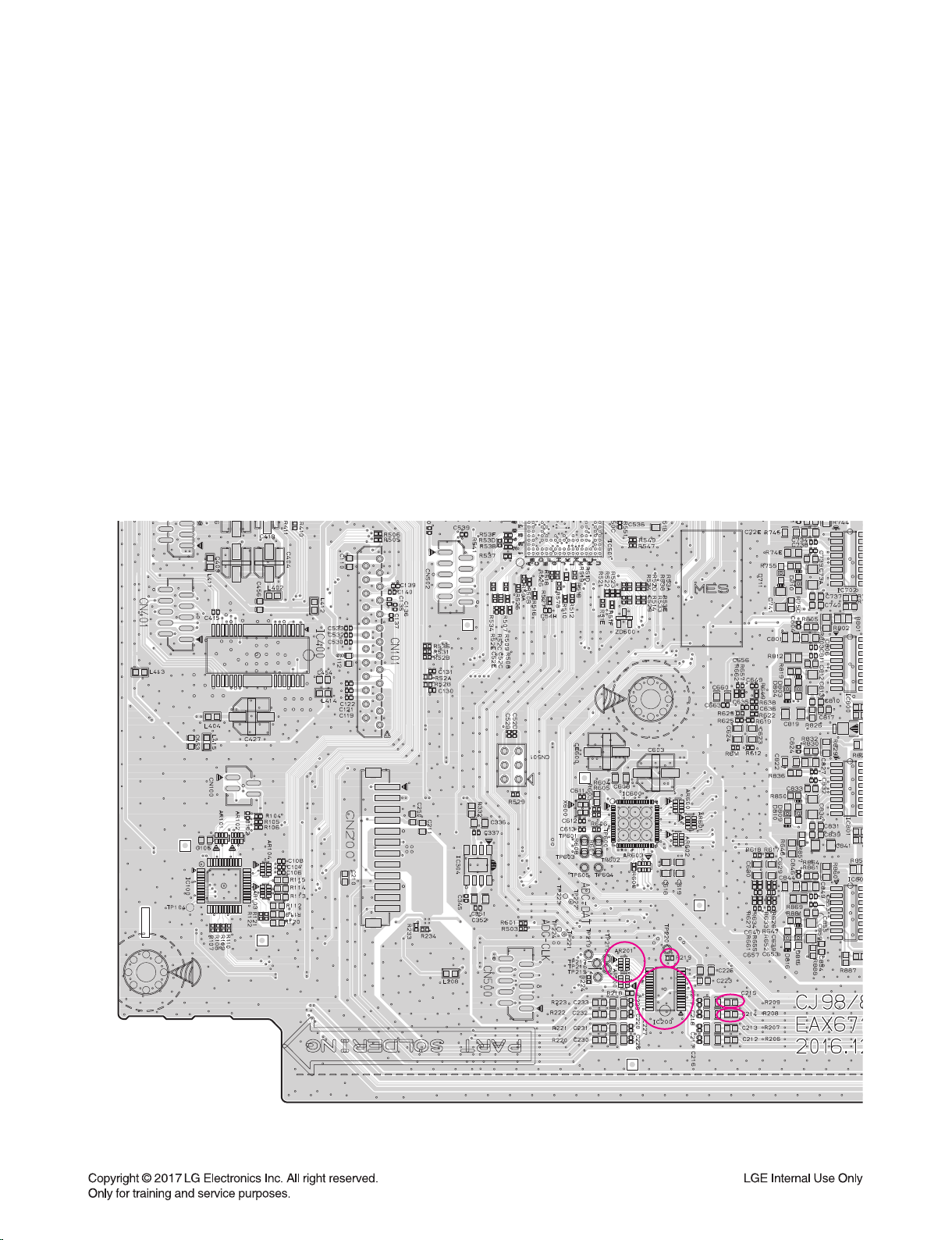
AR201
IC200
R219
R209
R208
MCS_MCLK to R219
AUX_L to R208
AUX_R to R209
MCS_LRCK to AR201
MCS_BCK to AR201
ADC_DATA to AR201
9. NO SOUND
There is no sound output in the AUX function, repair the set according to the following guide.
9-1. AUX FUNCTION
9-1-1. Solution
Replace IC200 on MAIN board.
9-1-2. How to troubleshoot (Countermeasure)
1) Check AUX_L/R signals to IC200(pin3, pin4).
2) Check if MCS_BCK, MCS_LRCK, & MCS_MCLK are entered from IC501 to IC200.
3) Check if ADC_DATA is entered from IC200 to IC501.
If no signal, check ADC_3.3 V & DVCC_3.3 V2 for IC200. If is NG, replace it a new one.
4) Check the following I2S signal flow from IC501 to IC600.
If there is any trouble, check the power for each IC.
The power is normal but, if the signal waveform to the IC is distorted or no signal, replace it with a new one.
5) Check if the digital audio AMP block is okay.
If AMP is damaged, replace it with a new one.
9-1-3. Service hint (Any picture/ Remark)
MCS_LRCK to AR201
MCS_BCK to AR201
ADC_DATA to AR201
< MAIN board top view >
3-19
AR201
IC200
MCS_MCLK to R219
AUX_R to R209
AUX_L to R208
R219
R209
R208
Page 49

IC200
PTB_L to pin21
PTB_R to pin22
ONE POINT REPAIR GUIDE
NO SOUND
There is no sound output in the PORT. IN function, repair the set according to the following guide.
9-2. PORT. IN FUNCTION
9-2-1. Solution
Replace IC200 on MAIN board.
9-2-2. How to troubleshoot (Countermeasure)
1) Check PT_L/ R signal from FRONT board to MAIN board.
2) Check if PT_L/ R is entered pin1 & pin3 of CN201.
3) Check PT_L/R signals to IC201(pin9, pin10).
4) Check if ADC_BCK, ADC_LRCK & DAC_MCLK are entered from IC501 to IC201.
5) Check if ADC_DATA is entered from IC201 to IC501.
If no signal, check +5 V & +3.3 V(ADC) for IC201. If is NG, replace it a new one.
6) Check the following I2S signal flow from IC501 to IC202.
If there is any trouble, check the power for each IC.
The power is normal but, if the signal waveform to the IC is distorted or no signal, replace it with a new one.
7) Check if the digital audio AMP block is okay.
If AMP is damaged, replace it with a new one.
9-2-3. Service hint (Any picture/ Remark)
IC600
PWM
POT. IN
IR AMP
MCS_MCLK
IC200
IC501
T-
ADC_DATA
POT_L/R
MCS_BCK
MCS_LRCK
MIX_DATA_OUT
Front
Board
< PORT. IN function signal fl ow diagram >
IC200
PTB_L to pin21
PTB_R to pin22
< MAIN board top view >
3-20
Page 50

ONE POINT REPAIR GUIDE
IC200
TUNER_L to pin26
TUNER_R to pin27
NO SOUND
There is no sound output in the TUNER function, repair the set according to the following guide.
9-3. TUNER FUNCTION
9-3-1. Solution
Replace IC200, TU500 on MAIN board.
9-3-2. How to troubleshoot (Countermeasure)
1) Check if TUNER_LR is entered from pin1 & pin3 of TU200 to IC200(pin1, pin2).
If no signals, check +3.3 V for tuner power.
Check if the tuner control signals(CLK, DAT, CE, RST, GPO2) are entered from IC501 to TU200.
If it doesn’t work, replace TUNER with a new one.
2) Check if MCS_BCK, MCS_LRCK & MCS_MCLK are entered from IC501 to IC200.
3) Check if ADC_DATA is entered from IC200 to IC501.
If no signal, check +3.3 V(ADC) for IC200. If is NG, replace it a new one.
4) Check the following I2S audio signal flow from IC501 to IC600.
If there is any trouble, check the power for each IC.
The power is normal but , if the signal waveform to the IC is distorted or no signal, replace it with a new one.
5) Check if the digital audio AMP block is okay.
If AMP is damaged, replace it with a new one.
9-3-3. Service hint (Any picture/ Remark)
T-
IC200
MCS_MCLK
IC501
IC600
PWM
< TUNER function signal fl ow diagram >
TUNER_L/R
ADC_DATA
MCS_BCK
MCS_LRCK
MIX_DATA_OUT
TUNER
IR AMP
IC200
TUNER_L to pin26
TUNER_R to pin27
< MAIN board top view >
3-21
Page 51

ONE POINT REPAIR GUIDE
IC201
MIC_OUTPUT. pin3
MIC_IN_DATA. pin2
MCS_MCLK to R219
MCS_LRCK to AR201
MCS_BCK to AR201
ADC_DATA to AR201
IC200
NO SOUND
There is no sound output in the MIC IN function, repair the set according to the following guide.
9-4. MIC IN FUNCTION
9-4-1. Solution
Replace IC200, IC201 on MAIN board.
9-4-2. How to troubleshoot (Countermeasure)
1) Check MIC_SIG signal to pin6 of CN200.
If no signal, check the signal to pin7 of CN3M01 on the FRONT board.
Check if the signal is entered from pin6 of CN200 to MAIN board.
2) Check if MIC_SIG is entered from pin6 of CN200 to pin2, pin13 to IC201(MIC AMP).
3) Check if the amplified signal comes out from pin3 & pin12 of IC201.
If no signal output, check +3.3 V for IC201, replace IC201 with a new one if it has a problem.
4) Check if MCS_BCK, MCS_LRCK, & MCS_MCLK are entered from IC501 to IC200.
5) Check if ADC_DATA is entered from IC200 to IC501.
If no signal, check +3.3 V(ADC) for IC200. If is NG, replace it a new one.
6) Check the following I2S signal flow from IC501 to IC600.
If there is any trouble, check the power for each IC.
The power is normal but, if the signal waveform to the IC is distorted or no signal, replace it with a new one.
7) Check if the digital audio AMP block is okay.
If AMP is damaged, replace it with a new one.
9-4-3. Service hint (Any picture/ Remark)
MCS_MCLK to R219
MCS_LRCK to AR201
MCS_BCK to AR201
ADC_DATA to AR201
IC200
< MAIN board top view >
IC201
MIC_IN_DATA. pin2
MIC_OUTPUT. pin3
< MAIN board bottom view >
3-22
Page 52

ONE POINT REPAIR GUIDE
BT_TX. pin4
BT_RX. pin6
BT_RTS. pin7
BT_CTS. pin8
CN500
BT_TX. R519
BT_RTS. R51D
BT_RX. R51B
BT_CTS. R512
NO SOUND
There is no sound output in the Bluetooth function, repair the set according to the following guide.
9-5. BLUETOOTH FUNCTION
9-5-1. Solution
Replace IC501 on the MAIN board or bluetooth module on the FRONT Panel.
9-5-2. How to troubleshoot (Countermeasure)
1) Check BT_RX, BT_TX signal to pin4, pin6 of CN504.
If no signal, check the signal to pin4, pin6 and pin10 (+3.3 V) of on the Bluetooth module and cable
connection state.
If there are no signal out from module, replace new module.
2) Check if BT_RX/ TX is entered from pin4, pin6 of CN504 to pin K1, pin L1 to IC501(DSP).
3) Check if MCS_BCK, MCS_LRCK & MIX_DATAN is entered from IC501 to IC202.
If no signal, check VCC12(+1.2 V) for IC501. If it is abnormal, change replace it a new one.
4) Check the following I2S signal flow from IC501 to IC202.
If there is any trouble, check the power for each IC. If the signals are abnormal, replace it a new one.
5) Check if the digital audio AMP block is okay.
If AMP is damaged, replace it with a new one.
9-5-3. Service hint (Any picture/ Remark)
B/T Module
BT_RX,
BT_TX
IC501
IC600
PWM
MCS_BCK
MCS_LRCK
MIX_DATA_OUT
IR AMP
BT_TX. pin4
BT_RX. pin6
BT_RTS. pin7
BT_CTS. pin8
BT_TX. R519
CN500
BT_RTS. R51D
BT_RX. R51B
BT_CTS. R512
3-23
< MAIN board top view >< MAIN board bottom view >
Page 53

ONE POINT REPAIR GUIDE
VFD_STB,
VFD_CLK,
VFD_DO
10. VFD IS NOT DISPLAYED WHEN POWER ON THE SET
When power on the set, any icons or characters on VFD are not displayed.
10-1. VFD (VFD301)
10-1-1. Solution
Please check and replace VFD301 on FRONT board.
10-1-2. How to troubleshoot (Countermeasure)
1) Check if VH, F+ and F-, DVCC_3.3V are output from SMPS to VFD via the MAIN board.
2) Check if the IC501 outputs VFD_CLK, VFD_STB, and VFD_DO to the FRONT board.
3) Check if the VH, FRONT_12V, SW on the FRONT board.
If the VH from VFD(DGND, VDD) isn’t output, replace VFD with a new one.
10-1-3. Service hint (Any picture/ Remark)
VFD_STB,
VFD_CLK,
VFD_DO
< FRONT circuit > < FRONT circuit >
3-24
Page 54

ELECTRICAL TROUBLESHOOTING GUIDE
1. POWER SUPPLY ON SMPS BOARD
No output 5.1 VA
Is the F901 normal?
YES
Is BD901 normal?
YES
Is the VCC
(11 V ~ 25 V) supplied to IC901
pin4?
YES
Power line of MAIN PCB is short.
NO
NO
NO
Replace F901 (same fuse).
Replace BD901.
Is D960, D961 normal?
Check or replace D960, D961.
No 12 V
VCC 12 VA supplied to IC951
‘HIGH’ signal at IC951
check line of MAIN PCB is short or not.
Is the
pin1?
YES
Is there
pin4?
YES
Check IC951 and replace.
Or
NO
NO
Check or replace D963.
Check P_CTL from μ-com.
3-25
Page 55

ELECTRICAL TROUBLESHOOTING GUIDE
POWER SUPPLY ON SMPS BOARD
No -5 V
VCC -7 VA supplied to IC953
Check or replace Q953, Q957.
check line of MAIN PCB is short or not.
No output AMP gate line
Is the
pin2?
YES
Is there
‘H’ signal at Q953
Base?
YES
Or
NO
NO
Is the D959 normal?
YES
Check or replace Q951.
Check P_CTL
from μ-com.
NO
Check or replace D959.
Is the VCC
13 VA supplied to IC952
pin1 to pin3?
Check and replace IC952.
check line of MAIN PCB is short or not.
Or
NO
Is the R952 normal?
YESYES
Check or replace D952, D959.
3-26
NO
Check or replace R952.
Page 56

ELECTRICAL TROUBLESHOOTING GUIDE
POWER SUPPLY ON SMPS BOARD
No AMP output
Is the
C904 voltage
about 390 V?
YES
Is F911 normal?
NO
NO
YES
Is the
PFC P.CTL OK?
YES
Is the
VCC 12 V supplied to
IC904 pin16?
YES
Check or replace
IC904, Q907 ~ Q910.
Is the
AMP P.CTL OK?
YES
Is the
VCC 12 V supplied to
IC902 pin2?
NO
NO
NO
NO
Check PFC P.CTL
from μ-com.
Replace D908, Q955, PC903.
Check AMP P.CTL
from μ-com.
Replace D908, Q956, PC902.Replace F911.
NO
Is Q905, Q906 OK?
NO
Replace Q905, Q906.
YES
Check or replace IC902 and
check Q905, Q906 gate(pin1)
Components (Resistors, Diodes).
3-27
Check or replace D954, D955.
Check line of MAIN PCB is short or not.
Page 57

ELECTRICAL TROUBLESHOOTING GUIDE
2. SYSTEM PART
Power on.
“HELLO”
Display on FLD
OK?
YES
When turn
the volume, count is
change?
YES
NO
NO
CN101
cable connection
OK?
YES
CN101
pin11, 22, 25,power
OK?
YES
CN101
pin5, 6, 7 data signal
OK?
YES
Check
CN101 pin3, 4 I2C data
OK?
YES
NO
NO
NO
NO
NO
Check FFC cable.
Check SMPS board.
Check MAIN board.
Replace VFD301.F+/- & VH voltage OK?
Check FFC cable.
FRONT board OK.
Check MAIN board.
3-28
Page 58

ELECTRICAL TROUBLESHOOTING GUIDE
3. NO AUDIO CHECK
CD FUNCTION
Can
disc insert?
YES
Disc reading OK?
YES
NO
NO
LOAD +, - OK?
YES
Is motor impedance
about 12 Ω?
OPU driving
(Focusing & Tracking) OK?
Check OPU.
(Pick-up module)
NO
NO
NO
NO
Is Motor_open/ close OK?
(IC400 pin6, 7)
YES
Check IC501.
Check loading motor.
Check IC400.
NO
Focusing/
Tracking/ Sled signal
OK?
YES
MON_MPD(CN400 pin22)
About 180 mV?
IC401 pin34 ~ 36
I2S output signal OK?
YES
IC501 pin N1, N2, N4
I2S input signal OK?
YES
A
NO
NO
IC401
RF & Servo signal
OK?
YES
Check IC501.
3-29
NO
Check FFC cable
to CN400, CN401.
Page 59

ELECTRICAL TROUBLESHOOTING GUIDE
NO AUDIO CHECK
USB play
When insert USB,
IC501 pin U7, U8, A7, A8
USB_D signal OK?
YES
A
AUX
NO
USB power USB_5 V
IC303
OK?
YES
NO
Replace IC303.
pin 3, 4 AUX input signal
IC200
OK?
YES
IC200
pin15, 16, 17 I2S input signal
OK?
YES
IC200
pin18 ADC_data output signal
OK?
YES
A
NO
NO
NO
Check audio cable.
Check IC501.
Replace IC200.
3-30
Page 60

ELECTRICAL TROUBLESHOOTING GUIDE
NO AUDIO CHECK
POT. IN
pin29, 30 POT. IN input signal
IC200
OK?
YES
IC200
pin15, 16, 17 I2S input signal
OK?
YES
IC200 pin18
ADC_data output signal
OK?
YES
A
TUNER
NO
NO
NO
Check FRONT board.
Check IC501.
Replace IC200.
IC200 pin1, 2
TUNER_L/R input signal
OK?
YES
IC200
pin15 ~ 17 I2S input
signal OK?
YES
IC200
pin18 ADC data output
signal OK?
YES
A
NO
NO
NO
TUN200
TUNER_L/R output
signal OK?
YES
Check IC501.
Replace IC200.
3-31
NO
Check +3.3 V of TUN200.
Page 61

ELECTRICAL TROUBLESHOOTING GUIDE
NO AUDIO CHECK
A
YES
pin D1,D2,E1 I2S Clock signal
IC501
OK?
YES
IC501
pin E2 I2S data signal
OK?
YES
IC600
PWM data output signal
OK?
YES
B
NO
NO
NO
Check IC501.
Check IC501.
Replace IC600.
3-32
Page 62

ELECTRICAL TROUBLESHOOTING GUIDE
NO AUDIO CHECK
B
Pin39 ~ 50 of IC600
FL/FR± signal OK?
YES
IC601,IC603
FL/FR audio signal OK?
YES
Pin13
of IC700, IC801 FL/FR
audio signal OK?
YES
NO
Check IC600.
NO
Check IC601,IC603
NO
Check IC700, IC801.
NO
Check IC600.
NO
Check IC602
NO
Check IC702.
Pin45, 46 of IC600
SW1± signal OK?
YES
IC602
SW1 audio signal OK?
YES
Pin13 of IC702
SW1 audio signal OK?
YES
±66 V, -12 V, ±5 V
power voltage OK?
YES
Q700, Q701,
Q802, Q803
OK?
YES
NO
Check SMPS.
NO
Check Q700, Q701,
Q802, Q803.
Check speaker cable connection.
OK
3-33
NO
Check SMPS.
NO
Check Q706, Q707.
±66 V, -12 V, ±5 V
power voltage OK?
YES
Q706, Q707
OK?
YES
Page 63
WAVEFORMS OF MAJOR CHECK POINT
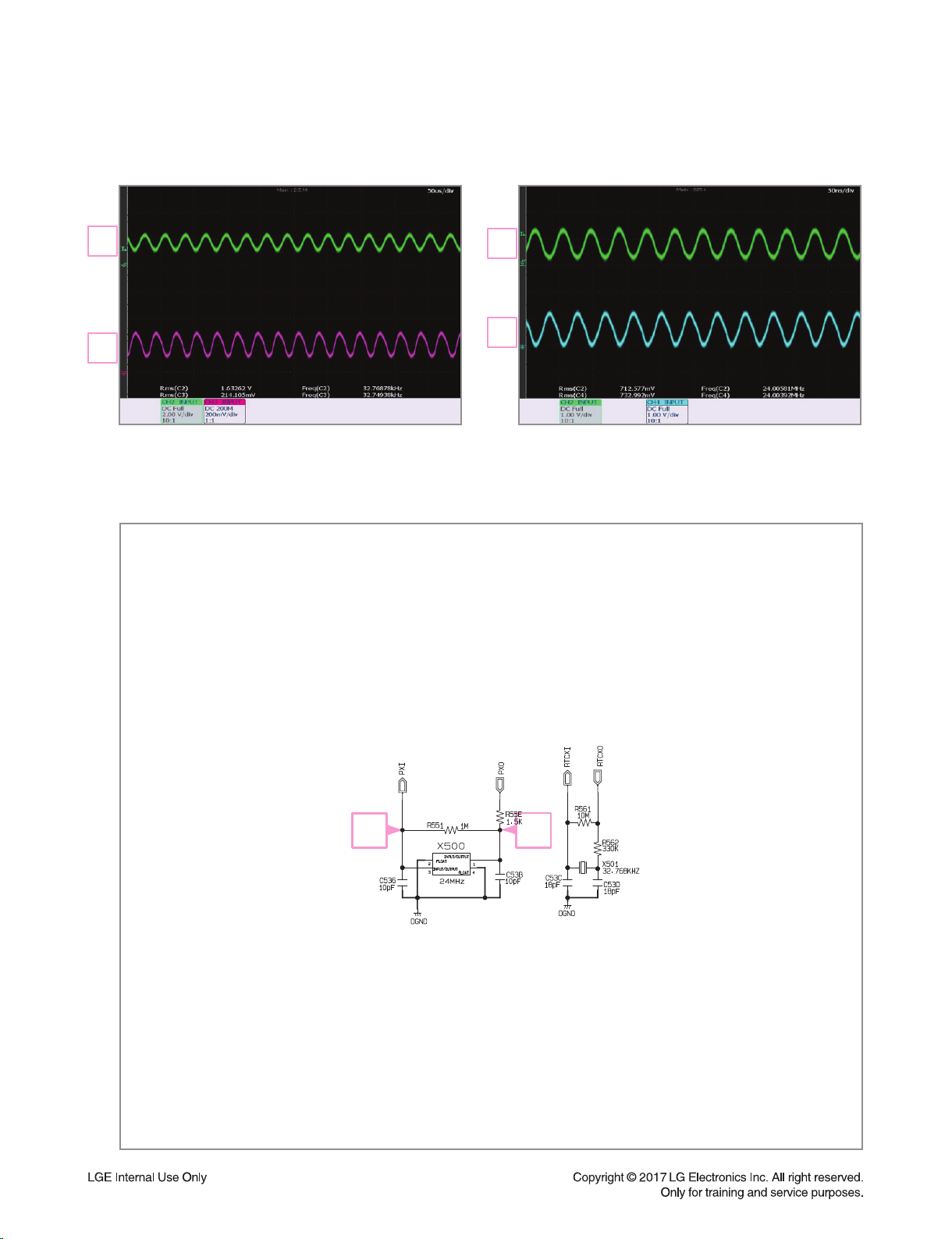
XI
XO
XI
XO
1. DSP (IC501)
X
1
2
Fig 1-1. Crystal of RTC 32.768 MHz
(Both ends of R561) X501
This model is not used.
3
4
X
Fig 1-2. Crystal of system 24 MHz
( MAIN DSP : R551, C53B) X500
3
4
3-34
Page 64

2. PWM (IC600)
XI
XO
X
5
7
8
6
9
Fig 2-1. Crystal 24.576 MHz
(IC600 pin4, pin5) X600
Fig 2-2. DSP to PWM I2S
(IC600 pin26 ~ pin30)
9
87
6
5
3-35
Page 65

3. SERVO (IC401)
XI
XO
X
10
11
12
Fig 3-1. Crystal 16.9344 MHz
(X400)
Fig 3-2. CD-16M
(IC401 pin31)
11
10
12
3-36
Page 66

4. MOTOR DRIVER (IC400)
13
17
14
15
16
19
20
Fig 4-1. LO- & LO+/ MOT_OPEN &
MOT_CLOSE for Driving TRAY Motor
(IC400 pin6, pin7, pin9, pin10)
18
Fig 4-2. SL- & SL+ for Driving SPINDLE Motor
(IC400 pin11, pin12)
Fig 4-3. SP- & SP+ for Driving SPINDLE Motor
(IC400 pin17, pin18)
16
14
15
13
17
18
20
19
3-37
Page 67

5. ADC 6. USB
21
22
24
23
25
Fig 5. ADC I2S
(IC200 pin16, pin17, pin18)
Fig 6. USB D+/ D-
(CN503 pin4, pin5, pin7, pin8)
2524
23
22
21
3-38
Page 68

7. BLUETOOTH
BT_TX
BT_RX
BT_RST
BT_TX
BT_RX
BT_RST
BT_TX
BT_RX
BT_RST
26
27
28
B
Fig 7. BT_TX/ BT_RX/ BT_RST
28 27 26
3-39
Page 69

3-40
Page 70

3-41 3-42
IC501
DSP
IC401
RF IC
IC600
PWM
IC100
MICOM
IC200
ADC
IC503
F/S 16M
IC504
SDRAM
IC400
Motor DR
Tuner
MIC
2
MIC
1
PTB
USB1
USB2
MAIN
BT
module
AUX In
MD
SMPS
Harness
FFC
FL
RL FR
RR W1 W2
Party Thruster
JACK
4P
FRONT
6P
12P
12P
6P
12P
12P
8P
25P
10P
8P
25P
10P
23P
10P
23P
WIRING DIAGRAM
Page 71

3-43 3-44
BLOCK DIAGRAM
(±5V)
(±66V)
DRIVER OP AMP
FET
X 2
DRIVER OP AMP
FET
IRF6775
X 2
DRIVER
OP AMP
FET
IRF6775
X 2
DRIVER OP AMP
FET
IRF6775
X 2
DRIVER
OP AMP
FET
IRF6775
X 2
IC501
Main DSP
(3.3V, 1.2VA)
DECK
MECHANISM
M
P/UP
(VCC50)
FRONT
VFD
Volume/
Key/switch
(+3.3VA,+12V)
Motor Drive
USB1
USB2
SERVO
(4؎ܓ)
IC201
ADC
IC30A1
PRE,AMP
IC202
PWM
DRM_WEN/CAS/
RAS/SEL/CLK/CKE
AMP_OSC
ADC_DATA
MCS_BCK/LRCK/MCLK
MID L
HIGH L
LOW 1
MID R
HIGH R
IR_IN_RL
RL_OUT_P/N
FL_OUT_P/N
RR_OUT_P/N
FR_OUT_P/N
M00_15
A00_16
SF_DI/DO
SF_CS/SCK
VFD_STB/CLK/DO/RST
MAIN VOL_A/B ,
KEY 1/2/3
OP_SW,CL_SW,UP_SW,DN_SW,D_SENSE
MOT_MUTE,CLOSE,OPEN
A,B,C,D,E,F,PD
LD
SPDO/SLDO
/FOD/TRD
LOAD± ,SLED±,
SPIN±,TR±,F±
D2S+/ -
IR_IN_FL
IR_IN_SW1
IR_IN_RR
IR_IN_FR
PWM_DAT/CLK/RST/DAT
CD_RW/MCLK/LRCK/BCK,
CD_DAT
CD_RST
UART_RX/TX
IC101
MICOM
SCRATCH A/B,
TOP_LED, FRONT_AGL,
MID_AGL, WOOFER_AGL
MIC_DET, PTB_DET,
SEARCH A/B
SW1_OUT_P/N
DRIVER
FET
IRF6775
X 2
LOW 2
IR_IN_SW2
32MB(256Mb )
SDRAM
16MB(128Mb )
S/Flash
8MB(64Mb )
S/Flash
SF_DI/DO
SF_CS/SCK
FAN_CTRL
MIC_DATA_IN
AUX
FM/AM
PTB
MIC1
MIC2
IC603
SLIDE_0
Party Thruster
SPK_EXP
CLK/DAT/LAT
SPK LED
LIGHTING
MIX_DATA
CD
BT
Page 72

CIRCUIT VOLTAGE CHART
1. CAPACITOR VOLTAGE
3-45 3-46
Location
Value Capacitor
(uF)
Voltage_Spec
(V)
100 V - 10 % 240 V/ 50 Hz + 10 %
Measured voltage
(V)
Measured voltage
(V)
SMPS Board
C904 270 uF 450 V 393 393
C926 47 uF 50 V 7.1 7.15
C927 47 uF 50 V 7.2 7.2
C930 68 uF 450 V 138 336
C936 1000 uF 16 V 5.09 5.11
C937 2200 uF 16 V 5.15 5.15
C944 1000 uF 25 V 13 13.1
C948 220 uF 25 V 7.5 7.6
C957 220 uF 25 V 12.98 12.98
C958 100 uF 16 V 11.9 11.89
C963 3300 uF 25 V 16.3 16.3
C964 220 uF 25 V 12.03 12.1
C966 1000 uF 80 V 67 66.9
C968 1000 uF 80 V 66 66
MAIN/ FRONT Board
C318 47 uF 16 V 3 3
C328 47 uF 16 V 6 6
C334 1 uF 50 V 31 31
C335 1 uF 50 V 18 18
C336 1 uF 50 V 21 21
C337 1 uF 50 V 18 18
C402 100 uF 16 V 5 5
C404 47 uF 16 V 3.3 3.3
C409 47 uF 16 V 3.3 3.3
C416 47 uF 16 V 1.7 1.7
C418 3.3 uF 50 V 1.7 1.7
C427 220 uF 16 V 5.1 5.1
C603 220 uF 6.3 V 1.3 1.3
C744 100 uF 16 V 0.04 0.04
C867 2200 uF 80 V 65 65
C868 2200 uF 80 V 65 65
CE300 100 uF 16 V 5.1 5.1
CE301 220 uF 6.3 V 3 3
CE600 220 uF 6.3 V 3.25 3.25
CE800 1000 uF 80 V 34 34
CE801 1000 uF 80 V 34 34
Page 73

3-47 3-48
PRINTED CIRCUIT BOARD DIAGRAMS
1. SMPS P.C.BOARD DIAGRAM
(TOP VIEW)
Page 74

3-49 3-50
SMPS P.C.BOARD DIAGRAM
(BOTTOM VIEW)
NOTE) Warning
Parts that are critical with respect to risk
of fire or electrical shock.
Page 75

3-51 3-52
2. MAIN P.C.BOARD DIAGRAM
(TOP VIEW)
Page 76

3-53 3-54
MAIN P.C.BOARD DIAGRAM
(BOTTOM VIEW)
Page 77

3-55 3-56
3. FRONT P.C.BOARD DIAGRAM
(TOP VIEW)
Page 78

3-57 3-58
FRONT P.C.BOARD DIAGRAM
(BOTTOM VIEW)
Page 79

3-59 3-60
4. JACK P.C.BOARD DIAGRAM
(TOP VIEW)
(BOTTOM VIEW)
Page 80

SECTION 4
MECHANISM (DM14B)
CONTENTS
DECK MECHANISM DISASSEMBLY
1. Cover Top ............................................................................................................................................... 4-2
2. Clamp Assembly ..................................................................................................................................... 4-2
2-1. Plate ................................................................................................................................................. 4-2
2-2. Magnet ............................................................................................................................................. 4-2
2-3. Clamp ............................................................................................................................................... 4-2
3. Tray Disc ................................................................................................................................................. 4-3
4. Pick Up Assembly ................................................................................................................................... 4-4
5. Base Up/Down ........................................................................................................................................ 4-4
6. Belt Loading ............................................................................................................................................ 4-5
7. Gear Pulley ............................................................................................................................................. 4-5
8. Gear Loading .......................................................................................................................................... 4-5
9. Guide ....................................................................................................................................................... 4-5
10. Deck PCB Assembly ............................................................................................................................... 4-5
11. Motor Assembly ...................................................................................................................................... 4-5
12. FFC Cable ............................................................................................................................................... 4-5
DECK MECHANISM EXPLODED VIEW (DM14B) ........................................................................................... 4-6
4-1
Page 81

(S1)
DECK MECHANISM DISASSEMBLY
1
Cover Top
1
Clamp
Assembly
2
3
Clamp Assembly
Plate
Magnet
2
Clamp
(L1)
< Figure A >
1. Cover Top
1) Remove the 2 screws (S1).
2) Unhook the 4 Locking Tabs (L1) by using a
flat-head screwdriver.
3) Remove the Cover Top.
< Figure B >
2. Clamp Assembly
1) Place the Clamp Assembly as Figure B.
2) Bending the Cover Top in direction of
arrow (2) as Figure B.
3) Separate the Clamp Assembly from the
Cover Top.
2-1. Plate
1) Turn the Plate to a counterclockwise direction
and then lift up the Plate.
2) Remove the Plate.
2-2. Magnet
Remove the Magnet.
2-3. Clamp
Remove the Clamp.
4-2
Page 82

DECK MECHANISM DISASSEMBLY
Emergency eject hole
Tray Disc
2
1
< Bottom side view >
Tray Disc
< Figure C >
(H1)
MD Sub
Assembly
1 1
22
3
Tray Disc
< Figure D >
3) Grasp the both sides of the Tray Disc and lift
it up as Figure D, and then pull the Tray Disc
until it is separated from the MD Sub Assembly
completely.
3. Tray Disc
1)
Insert and push a flat-head screwdriver in the
Emergency eject hole (H1) at the right side, so
that the Tray Disc is ejected about 15 ~ 20 mm.
2) Pull the Tray Disc until it is locked.
Guide
Tray Disc
< Figure E >
Note
• When reassembling place the Guide as Figure E.
4-3
Page 83

DECK MECHANISM DISASSEMBLY
B
L
K
RED
B
RN
ORN
R
ED
B
K
Gasket Tape
Rubber
Damper
5
4
1
< Bottom side view >
FFC Cable
(S2)
2
Deck PCB
Assembly
3
Pick Up
Assembly
Base Up/Down
(L2)
Base Main
(D)
(B)
3
1
2
(H2)
Figure G-3
(A)
Figure G-2Figure G-1
(C)
Guide
(B)
Base
Up/Down
< Figure F >
4. Pick Up Assembly
1) Detach the Gasket Tape.
2) Disconnect the wires (BLK, RED, BRN, ORN)
from the Deck PCB Assembly by desoldering.
3) Remove the 4 screws (S2).
4) Disconnect the FFC Cable from the Pick Up
Assembly.
5) Remove the 4 Rubber Dampers.
< Figure G >
5. Base Up/Down
Unlock the Locking Tab (L2) in direction of arrow
and then lift up the Base Up/Down to separate it
from the Base Main.
Note
• When reassembling move the Guide in direction
of arrow (A) until it is positioned as Figure G-1.
• When reassembling insert the (B) portion of the
Base Up/Down in the (C) portion of the Guide as
Figure G-2.
• When reassembling insert the (D) portion of the
Base Up/Down in the Hole (H2) of the Base Main
as Figure G-3.
4-4
Page 84

DECK MECHANISM DISASSEMBLY
B
L
K
RED
B
RN
ORN
R
ED
B
K
Gear Loading
Gear Pulley
(L3)
< Bottom side view >
Belt Loading
Base Main
(A)
Figure H-1
Guide
(B)
Base Main
(L4)
< Bottom side view >
6. Belt Loading
Remove the Belt Loading.
7. Gear Pulley
Unlock the Locking Tab (L3) in direction of arrow
and then separate the Gear Pulley from the Base
Main.
8. Gear Loading
Remove the Gear Loading.
9. Guide
1) Move the Guide in direction of arrow (A) as
Figure H-1.
2) Separate the Guide from the Base Main.
Motor
Assembly
(S3)
< Figure H >
10. Deck PCB Assembly
11. Motor Assembly
12. FFC Cable
Deck PCB
< Bottom side view >
Deck PCB
Assembly
Assembly
1) Disconnect the wires (RED, BK) form the
Deck PCB Assembly by desoldering.
2) Remove the 1 screw (S3).
3) Separate the Deck PCB Assembly from the
Base Main.
Unlock the Locking Tab (L4) in direction of
arrow and then separate the Motor Assembly
from the Base Main.
Remove the FFC Cable.
4-5
Page 85

DECK MECHANISM EXPLODED VIEW (DM14B)
1439
1013
1026
1016
1015
1012
1003
1024
1437
1049
1020
1005
1004
1024
1001
1002
1024
A001
1030
1437
1024
1437
A006
1019
1018
1011
A005
1043
1045
1439
4-6
 Loading...