

Page 1

TABLE OF CONTENTS
INTRODUCTION....................................................................................................................................................3
FEATURES............................................................................................................................................................3
SPECIFICATIONS .............................................................................................................................................4~5
LOCATION OF CUSTOMER CONTROLS........................................................................................................6~7
DISASSEMBLY .................................................................................................................................................8~9
1. CABINET and CIRCUIT BOARD DISASSEMBLY.........................................................................................8
1-1. Bottom Chassis.........................................................................................................................................8
1-2. Front Bezel Assy.......................................................................................................................................8
1-3. Cabinet and Main Circuit Board ................................................................................................................8
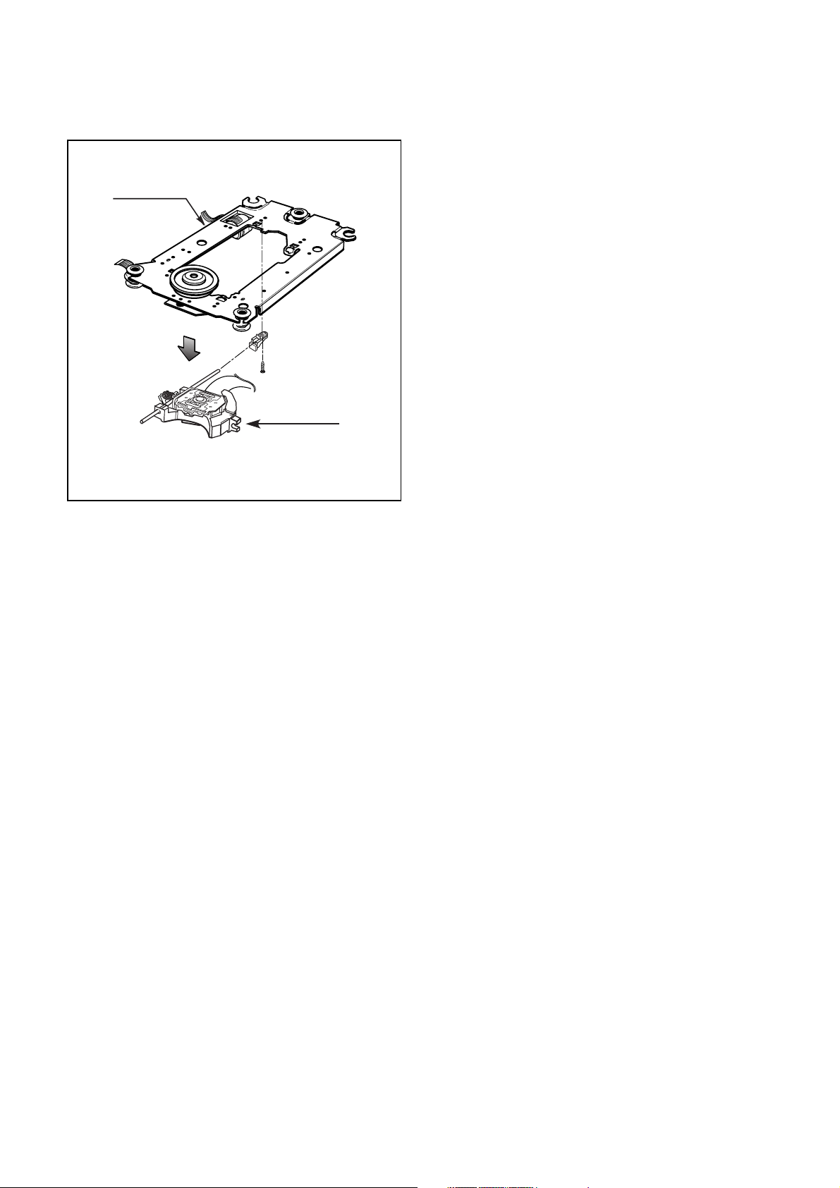
2. MECHANISM ASSY DISASSEMBLY ............................................................................................................8
2-1. Pick-up Unit...............................................................................................................................................8
2-2. Pick-up .....................................................................................................................................................9
GLOSSARY .........................................................................................................................................................10
EXPLODED VIEW .........................................................................................................................................11~12
MECHANICAL REPLACEMENT PARTS LIST.............................................................................................13~17
THE DIFFERENCES OF CD-R/CD-RW DISCS AND GENERAL CD-ROM .................................................18~24
1. Recording Layer...........................................................................................................................................18
2. Disc Specification.........................................................................................................................................18
3. Disc Materials...............................................................................................................................................19
4. Reading Process of Optical Disc..................................................................................................................20
5. Writing Process of CD-R Disc ......................................................................................................................21
6. Writing Process of CD-RW Disc...................................................................................................................21
7. Organization of the PCA, PMA and Lead-in Area ........................................................................................22
8. Function of PCA and PMA area ...................................................................................................................23
9. OPC and ROPC ...........................................................................................................................................23
10. Writing Process of DISC ............................................................................................................................24
INTERNAL STRUCTURE OF THE PICK-UP................................................................................................25~27
1. Block Diagram of the Pick-up.......................................................................................................................25
2. Pin Description .............................................................................................................................................26
3. Signal detection of the P/U...........................................................................................................................27
DESCRIPTION OF CIRCUIT .........................................................................................................................28~33
1. ALPC Circuit.................................................................................................................................................28
2. RF Amplifier Circuit ......................................................................................................................................30
3. Focus/Tracking/Sled Servo Circuit...............................................................................................................31
4. Spindle Servo Circuit....................................................................................................................................33
MAJOR IC INTERNAL BLOCK DIAGRAM AND PIN DESCRIPTION .........................................................34~53
TROUBLESHOOTING GUIDE ......................................................................................................................54~76
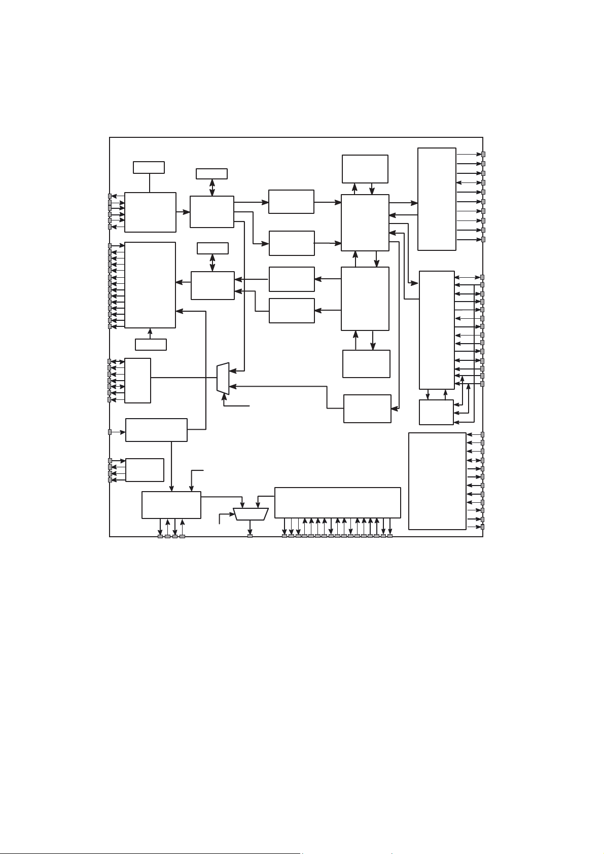
BLOCK DIAGRAM ........................................................................................................................................77~80
1. Overall Block Diagram .................................................................................................................................77
2. Power Block Diagram...................................................................................................................................78
3. Control Signal Block Diagram ......................................................................................................................79
4. Read/Write Signal Block Diagram................................................................................................................80
CIRCUIT DIAGRAM ......................................................................................................................................81~83
RINTED CIRCUIT BOARD DIAGRAM..........................................................................................................84~87
ELECTRICAL REPLACEMENT PARTS LIST ............................................................................................88~109
CAUTION - INVISIBLE LASER RADIATION WHEN OPEN AVOID EXPOSURE TO BEAM.
Page 2

3
INTRODUCTION
FEATURES
1. General
1) Enhanced IDE interface.
2) Internal 5.25 inch, halfheight CD-R/RW Drive.
3) 8 Mbytes buffer memory.
4) Audio CD like tray loading of a disc without using a caddy.
5) Power loading and power ejecting of a disc. The disc can also be ejected manually.
6) Supports Power saving mode and Sleep mode.
7) Vertical and Horizontal operation.
2. Supported disc formats
1) Reads and writes data in each CD-ROM, CD-ROMXA, CD-I FMV, Video CD, and CD-EXTRA
2) Reads data in Photo CD (Single and Multi session).
3) Reads and writes standard CD-DA.
4) Reads and writes CD-R discs conforming to “Orange Book Part 2”.
5) Reads and writes CD-RW discs conforming to “Orange Book Parts 3”.
3. Supported write method
1) Disc at once (DAO), Session at once (SAO), Track at once (TAO), Variable packet, Fixed packet, and
Multi-session.
4. Performance
1) Random 110 ms average access time.
2) Max 4,800 kB/sec (Max 32X) Sustained Transfer rate.
3) Supports real time error correction and real time layered error correction at each speed.
4) CD-R Record speed : 4X, 8X, 12X.
5) CD-RW Record speed : 2X, 4X, 8X.
6) PIO Mode 4 & Multi DMA Mode 2 Support.
7) MPC-3 Spec compliant.
8) Support CD-TEXT read/write.
5. Audio
1) Output 16 bit digital data over ATA interface.
2) 4 Times Digital Filter for CD Audio
3) Software Volume Control
4) Equipped with audio line output and headphone jack for audio CD playback.
5) Front panel Volume Control for Headphone Output.
This service manual provides a variety of service
information.
It contains the mechanical structure of the CDR/RW Drive and the electronic circuits in
schematic form. This CD-R/RW Drive was
manufactured and assembled under our strict
quality control standards and meets or exceeds
industry specifications and standards.
This CD-R/RW drive is an internal drive unit
designed for use with IBM PC, HP Vectra, or
compatible computer. It can write as much as 650
Mbytes of digital data into CD-R/RW disc, and can
read as much as 650 Mbytes of digital data stored
in a CD-ROM, CD-R and CD-RW disc.
This CD-R/RW Drive can easily meet the
upcoming MPC level 3 specification, and its
Enhanced Intelligent Device Electronics (E-IDE)
and ATAPI interface allows Plug and play
integration in the majority of today’s PCs without
the need of an additional interface card.
Page 3

4
SPECIFICATIONS
1. SYSTEM REQUIREMENTS
-CPU: IBM Compatible Pentium 233MHZ (or faster)
(For 12X Write speed, 350MHz or faster recommended.)
-32MB Memory or greater
2. SUPPORTING OPERATING SYSTEM
3. GENERAL
1) Host Interface.......................................................................................................................ATAPI compliant
2) Read Function
• Acceptable discs ...............................................................CD-ROM Mode1 (basic format), CD-ROM XA
CD-Audio
Mixed Mode (Audio and Data Combined)
Photo-CD (Single and Multi-Session)
CD-I Ready, Video CD
CD-Plus/CD-Extra,
CD-R (Conforming to “Orange Book Part2”)
CD-RW (Conforming to “Orange Book Part3”)
3) Write function
• Applied Format..................................................................CD-ROM Mode-1
CD-ROM XA
CD-Audio
Mixed Mode (Audio and Data Combined)
Video CD
CD-Plus/CD-Extra,
• Writing Method..................................................................Disc at once(DAO)
Session at once(SAO)
Track at once(TAO)
Variable packet writing
Fixed packet writing
Multi-session
4) Cache memory (R/W) .........................................................8 Mbyte
5) Disc diameter ......................................................................12 cm (8 cm Read only)
6) Data capacity (Yellow-Book)
• User Data/Block ................................................................2,048 bytes/block (Mode 1 & Mode 2 Form 1)
2,336 bytes/block (Mode 2)
2,324 bytes/block (Mode 2 Form 2)
2,352 bytes/block (CD-DA)
7) Rotational Speed
CD-Audio.............................................................................8x~20x(CAV) Approx.4000 rpm
CD-RW data ........................................................................10x~24x(CAV) Approx.5000 rpm
CD-ROM/CD-R data............................................................14x~32x(CAV) Approx. 7000 rpm
8) MTBF
• 125, 000 POH at an operating duty of 10% at room temperature.
• DOS 3.1 or Higher
• Windows ‘95/’98/’2000
• OS/2 Warp (Ver 3.0)
• Solaris Ver 2.4 or higher
• Linux Slackware Ver 2.3
• Windows NT 4.0 or later
Page 4
5
4. DRIVE PERFORMANCE
1) Data Transfer Rate
* Sustained Data Transfer Rate ..........................................150 Kbytes/s (1x)
300 Kbytes/s (2x)
600 Kbytes/s (4x)
1,200 Kbytes/s (8x)
2,100 to 4,800 Kbytes/s 14 to 32x CAV
* Burst Data Transfer Rate (ATAPI) ....................................16.67 Mbytes/sec (PIO Mode 4)
16.67 Mbytes/sec (MULTI-DMA Mode 2)
2) Average Access Time
Random Access ..................................................................110 ms Typical (Max.32X) : INCLUDING LATENCY
3) Data Buffer Capacity ...........................................................8 Mbytes
5. POWER REQUIREMENTS
1) Voltage
+5 V DC with +5% tolerance, less than 100 mVp-p Ripple voltage
+12 V DC with +5% tolerance, less than 100 mVp-p Ripple voltage
2) Current
• Hold Track State ...............................................................+5V DC 1.1A, +12 V DC 0.6A (Typical)
• Seeking & Spin up ............................................................+5 V DC 1.3A, +12 V DC 1.7A (Typical)
6. AUDIO PERFORMANCE
* CED-8120B FUNCTION TABLE
Item Typical Limit Test Signal Test Condition Note
Output Level
0.7 Vrms
+
10 % 1KHz 0 dB No Filter at 47 kΩ
S/N 80 dB 75 dB 1KHz 0 dB with IHF-A + 20KHz LPF at 47kΩ
THD 0.1 % 0.15 % 1KHz 0 dB with IHF-A + 20KHz LPF at 47kΩ
Channel
70 dB 65 dB 1KHz 0 dB with IHF-A + 20KHz LPF at 47kΩ
Separation
Frequency +
2dB
Response
H/P
Output Level
AUDIO OUT
+
3 dB 20Hz~18KHz 0 dB No Filter at 47 kΩ
0.6Vrms
+
20 % 1KHz 0dB No Filter H/P Volume MAX at 32 Ω
FFuunnttiioonn CCEEDD--88112200BB
• CD-R Writing speed 4x/8x/12x Data writing
• CD-RW Writing speed 2x/4x/8x Data writing
• CD-ROM Reading speed 32x Data transfer
MM OO DD EE LL
Page 5
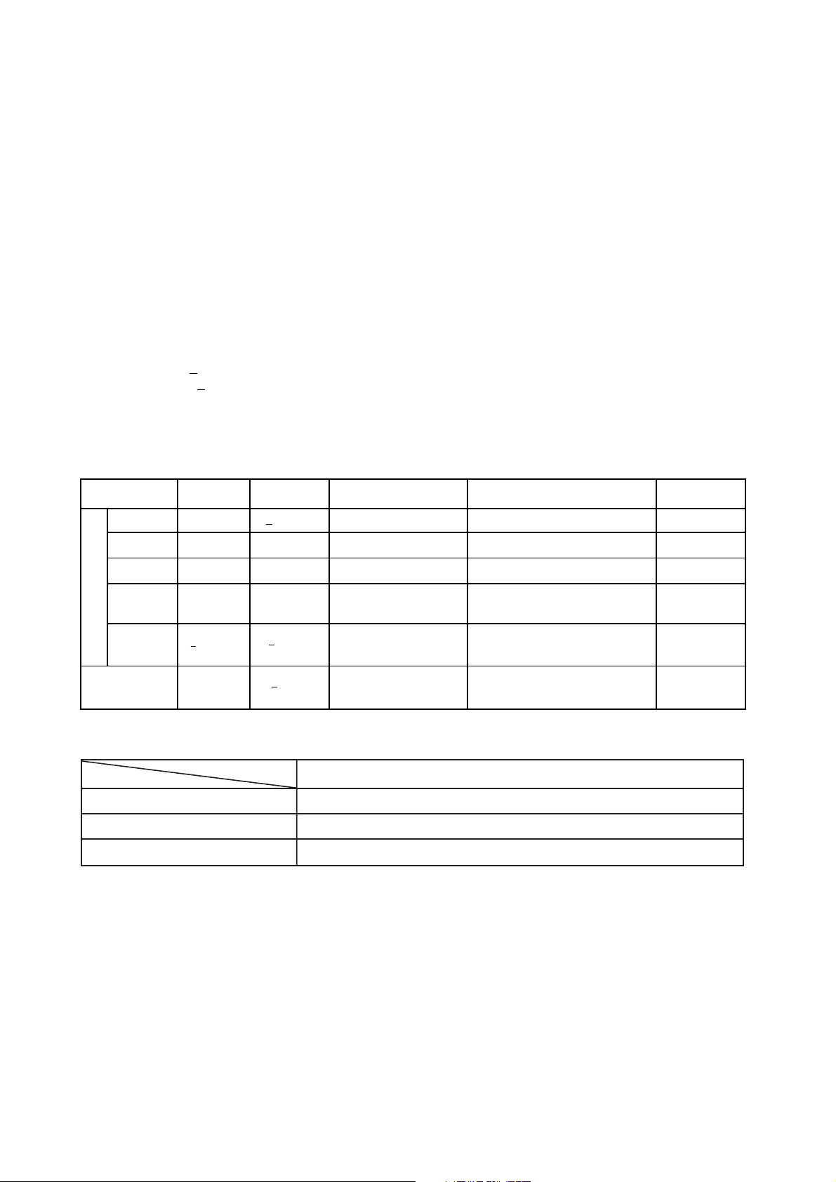
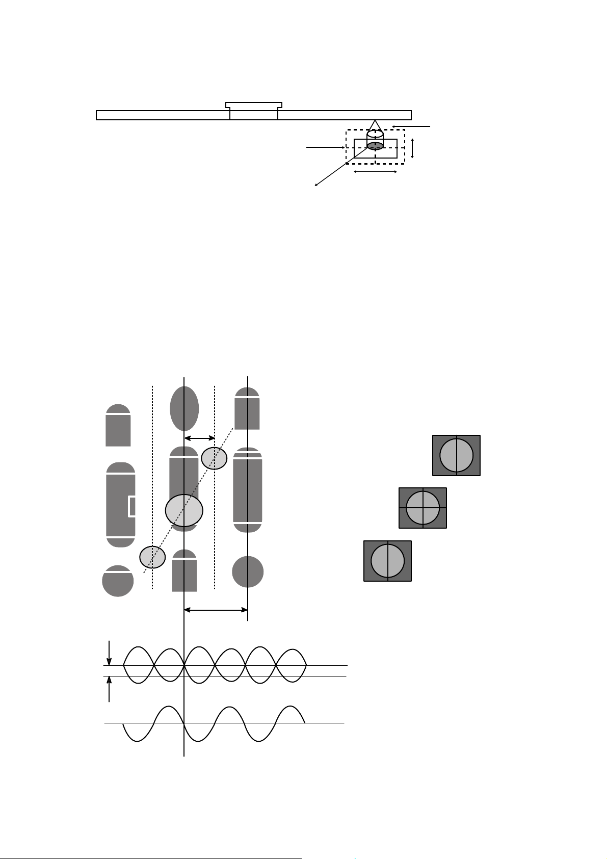
LOCATION OF CUSTOMER CONTROLS
6
1. Disc tray
This is the tray for the disc. Place the disc on the
ejected disc tray, then lightly push the tray (or
push the eject button) and the CD will be loaded.
NOTE: Don’t pull out or push in the disc tray
forcibly. This might cause damage to the loading
section of the drive.
2. Stop/Eject button
This button is pressed to open the CD tray.
This button works only when power is supplied to
the drive.
If an Audio CD is playing, pressing this button will
stop it, and pressing it again will open the tray.
3. Play/Skip button
When an Audio CD is in the disc drawer, pressing
this button will start playing Audio CDs from the
first track. If an Audio CD is playing, pressing this
button will skip to the next track.
4. Emergency Eject Hole
Insert a paper clip here to eject the Disc tray
manually or when there is no power.
5. Volume control
This is used to adjust the output volume of the
headphone jack. It can’t be used to adjust the
output volume for the audio output connectors on
the rear panel.
NOTE : Turn the volume down before turning on
the power. Sudden loud noises can damage your
hearing.
6. Headphone jack
This jack is for connecting headphones or minispeakers.
7. Drive activity indicators
Two colored LEDs are used to indicate the
operation of CD-R/RW Drive.
(1) Read
The orange color is displayed when the spindle
motor begins the Spin up operation: accessing
data, reading data, playing Audio, and up loading
tray.
(2) Write
The green color is flashed during disc writing
sessions.
READ
READ
WRITE
WRITE
Headphone Jack
Volume
Control
Drive Activity Indicators
Play/Skip Button
Stop/Eject Button
Disc Tray
Emergency Eject Hole
Front Panel
Page 6
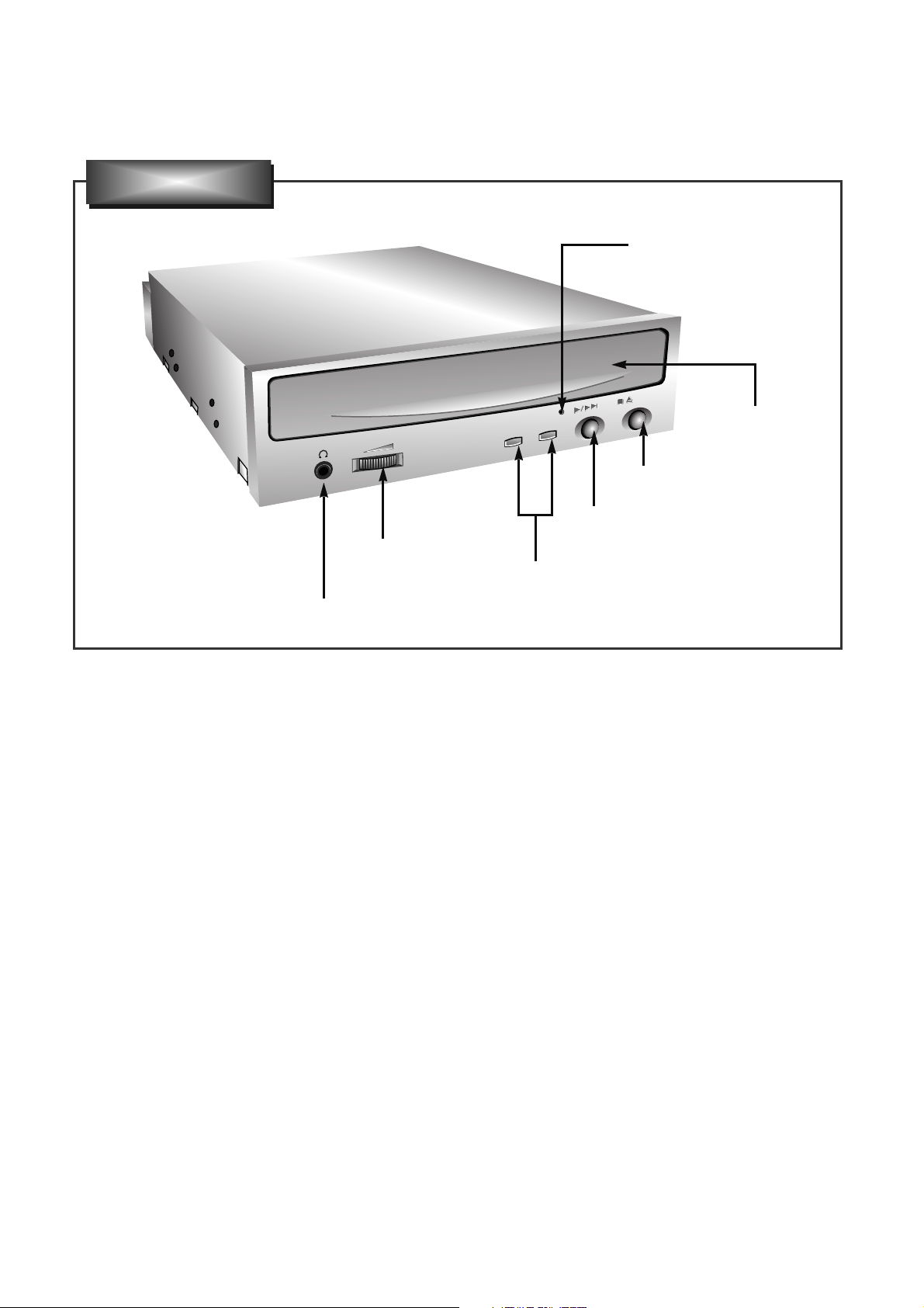
7
1. Power Connector
Connects to the power supply (5-and 12-V DC) of
the host computer.
NOTE : Be careful to connect with the proper
polarity. Connecting the wrong way may damage
the system (and is not guaranteed). Usually this
connector can only be attached one-way.
2. IDE Interface Connector
Connect to the IDE (Integrated Device
Electronics) Interface using a 40-pin flat IDE
cable.
NOTE : Do not connect or disconnect the cable
when the power is on, as this could cause a short
circuit and damage the system. Always turn the
power OFF when connecting or disconnecting the
cable.
3. Jumper Connector
This jumper determines whether the drive is
configured as a master or slave. Changing the
master-slave configuration takes effect after
power-on reset.
4. Analog Audio Output Connector
Provides output to a sound card (analog signal).
Generally you need this to play a regular audio
CD.
5. Digital Audio Output Connector
Provides output to a sound card (digital signal).
Digital Audio Output
Connector
Jumper Connector
Analog Audio Output Connector
IDE Interface Connector
Power Connector
Rear Panel
Page 7
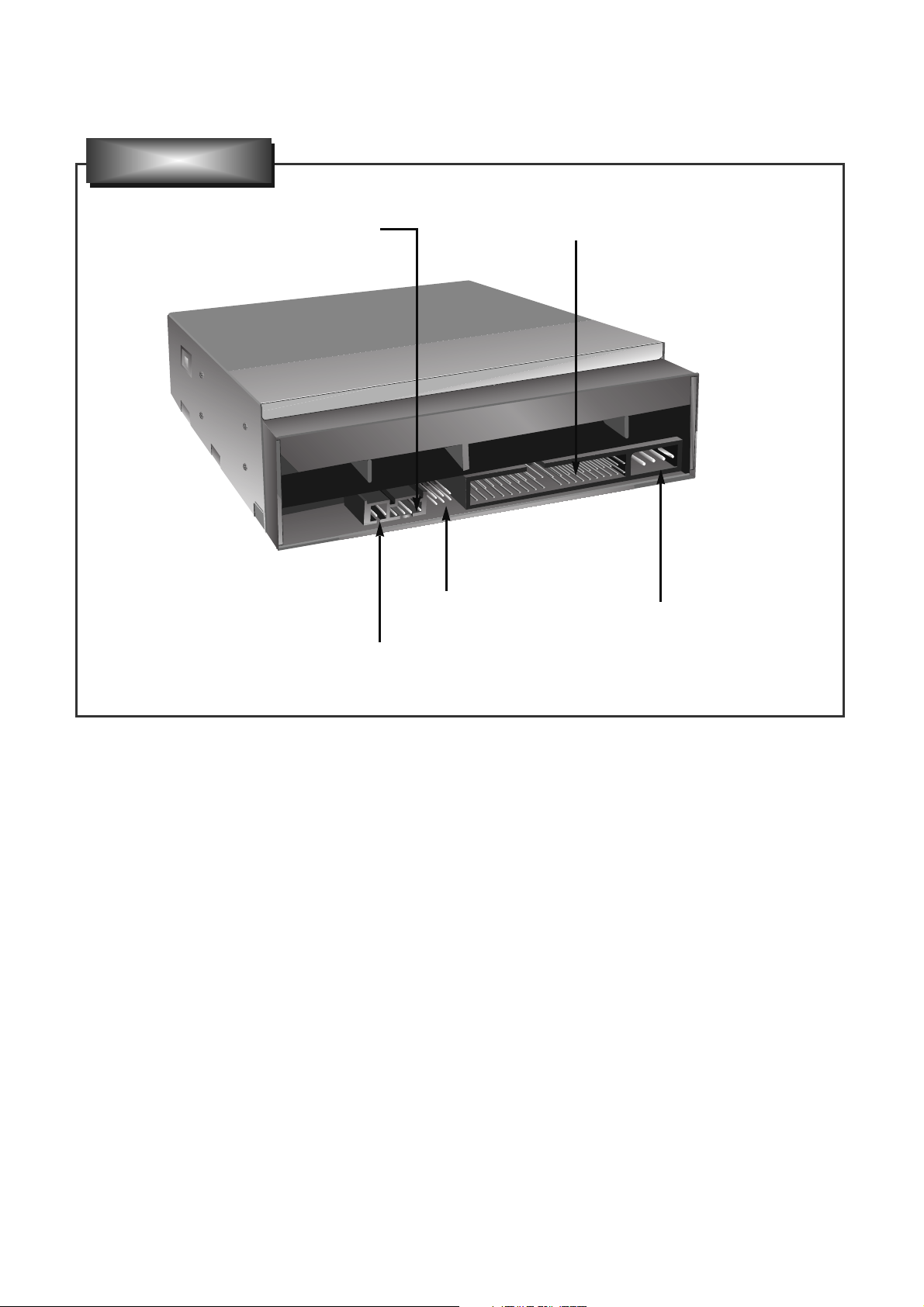
1. CABINET and CIRCUIT BOARD
DISASSEMBLY
1-1. Bottom Chassis
A. Release 4 screws (A) and remove the Bottom Chassis
in the direction of arrow (1). (See Fig.1-1)
1-2. Front Bezel Assy
A. Insert and press a rod in the Emergency Eject
Hole and then the CD Tray will open in the direction
of arrow (2).
B. Remove the Tray Door in the direction of arrow
(3) by pushing the stoppers forward.
C. Release 3 stoppers and remove the Front Bezel Assy.
1-3. Cabinet and Main Circuit Board
A. Remove the Cabinet in the direction of arrow (4).
(See Fig. 1-3)
B. Release 2 hooks (a) and remove the CD Tray
drawing forward.
C. Remove the Main Circuit Board in the direction of
arrow (5).
D. At this time, be careful not to damage the 4
connectors, are positioned at left side, of the Main
Circuit Board.
2. MECHANISM ASSY DISASSEMBLY
2-1. Pick-up Unit
A. Release screw (B).
B. Separate the Pick-up Unit in the direction of arrow (6).
(4)
(5)
Main
Circuit Board
Hooks (a)
Cabinet
Fig. 1-1
Fig. 1-2
DISASSEMBLY
8
Fig. 1-3
Mechanism Assy
Pick-up Unit
(B)
(6)
Fig. 2-1
(1)
(A)
Bottom Chassis
(A)
(A)
(A)
Tray Door
(3)
Stoppers
Emergency Eject Hole
(2)
Front Bezel Assy
CD Tray
Page 8
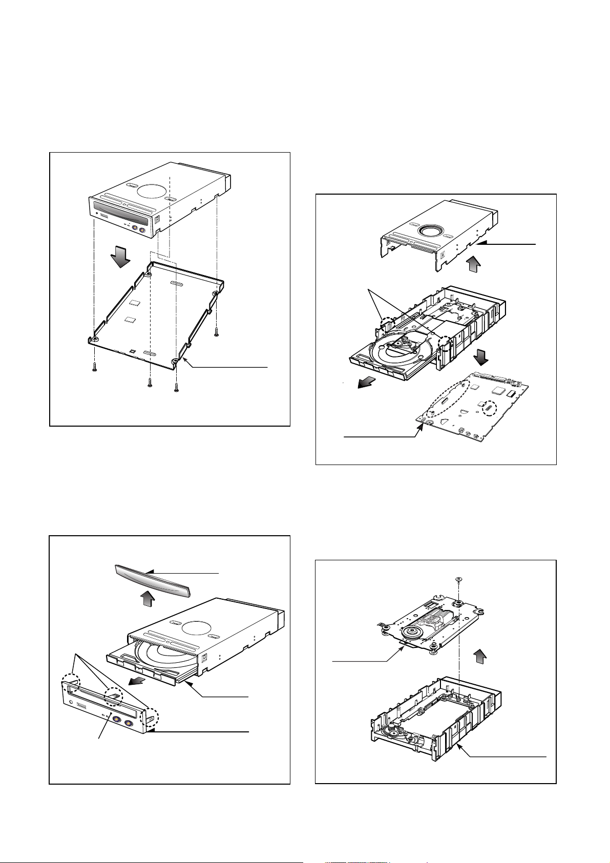
2-2. Pick-up
A. Release 1 screw (C) and remove the Pick-up.
Pick-up Unit
Pick-up
(C)
Fig. 2-2
9
Page 9

ATIP Absolute Time in Pre-groove. With an additional modulation of the “Wobble”, the “Groove” contains a time
code information.
Wobble The pre-groove in the Disc is not a perfect spiral but is wobbled.
With : – A typical amplitude of 30 nm
– A spatial peried of 54~64 µm
CW Continuous Wave. The laser light output is at a constant level.
DOW Direct Over-Write. The action in which new information is recored over previously recorded information in
CD-RW disc.
Overwrite
The action in which new information is recorded over previously recorded information.
(Pre-)Groove
The guidance track in which clocking and time code information is stored by means of an FM
modulated wobble.
Land Land is characterized in the following way:
When radial signals are concerned,land is defined as the area between the grooves.
When HF signal are concerned,land is defined as the area between the marks(pits) in tangential
direction.
Hybrid Disc A Multisession disc of which the first Session is mastered. On a hybrid disc, recorded and
mastered information may co-exist.
Mastered Information,stored as pits on the disc during the manufacturing process of the disc.
Information (when making the master)
OPC Optimum Power Control. Procedure is determined optimum recording power according to CD-
R/RW Media in recording start step.
ROPC Running OPC. The purpose is to continuously adjust the writing power to the optimum power
that is required.
When the optimum power may change because of changed conditions of disc and change in
operating temperature.
Jitter The 16 value of the time variation between leading and trailing edges of a specific (I3 … I11) pit
or land as measured by Time Interval Analysis.
Deviation The difference between a fixed value of Pit length and Land length.
TOC Table Of Contents : in the Lead-in Area the subcode Q-channel contains information about the
Tracks on the disc.
Packet A method of writing data on a CD in small increments.
Writing Two kinds of packets can be written : Fixed-length and Variable-length.
Write The shape of the HF write signal used to modulate the power of the laser.
Strategy The Write Strategy must be used for recordings necessary for disc measurements.
Information Wobble, ATIP, Disc Identification, Write Power, Speed Range OPC Parameters, etc are
Area recorded in the Information area of CD-RW Disc
Finalization The action in which (partially) unrecorded or logically erased tracks are finished and the Lead-in
and/or Lead-out areas are recorded or overwritten with the appropriate TOC subcode.
Logical Erase
A method to remove information from a disc area by overwriting it with an EFM signal containing
mode 0 subcode
A logically erased area is equivalent to an unrecorded
Physical Erase
The action in which previously recorded information is erased by overwriting with a CW laser
output.
After a Physical Erase action, the erased area on the CD-RW disc is in the unrecorded state
again.
Session
An area on the disc consisting of a Lead-in area, a Program area, a lead-out area.
Multi session
A session that contains or can contain more than one session composed Lead-in and Lead-out
GLOSSARY
10
Page 10
The differences of CD-R/CD-RW discs and General CD-ROM
1. Recording Layer
Recordable CD has a wobbled pre-groove on the surface of disc for laser beam to follow track.
2. Disc Specification
Read-only Disc
CD-R and CD-RW Disc
3~11T
1.6um
0.4~0.5 um
(Pit)Groove
Land
Track pitch(p)
Radial Direction
Iw
A
O
a
a
Groove
Land
Radial Error Signal
The Groove wobble
Average center
Actual center
CD-ROM CD-R CD-RW
Standard Yellow Book Orange Book II Orange Book III
Record Not available Write once Re-writable
I 11/Itop
> 0.6 > 0.6 0.55 > M11> 0.70
(HF Modulation)
Write Laser Power(mW) 10-30 mW 6-25 mW
Read Laser Power(mW) < 0.5 mW < 0.7 mW < 1.0 mW
Jitter < 35 nsec < 35 nsec < 35 nsec
Reflectivity (R
top) 70 % 65 % 15 % ~ 25 %
18
CD-ROM (READ-ONLY DISC)
a=30nm
Page 11
19
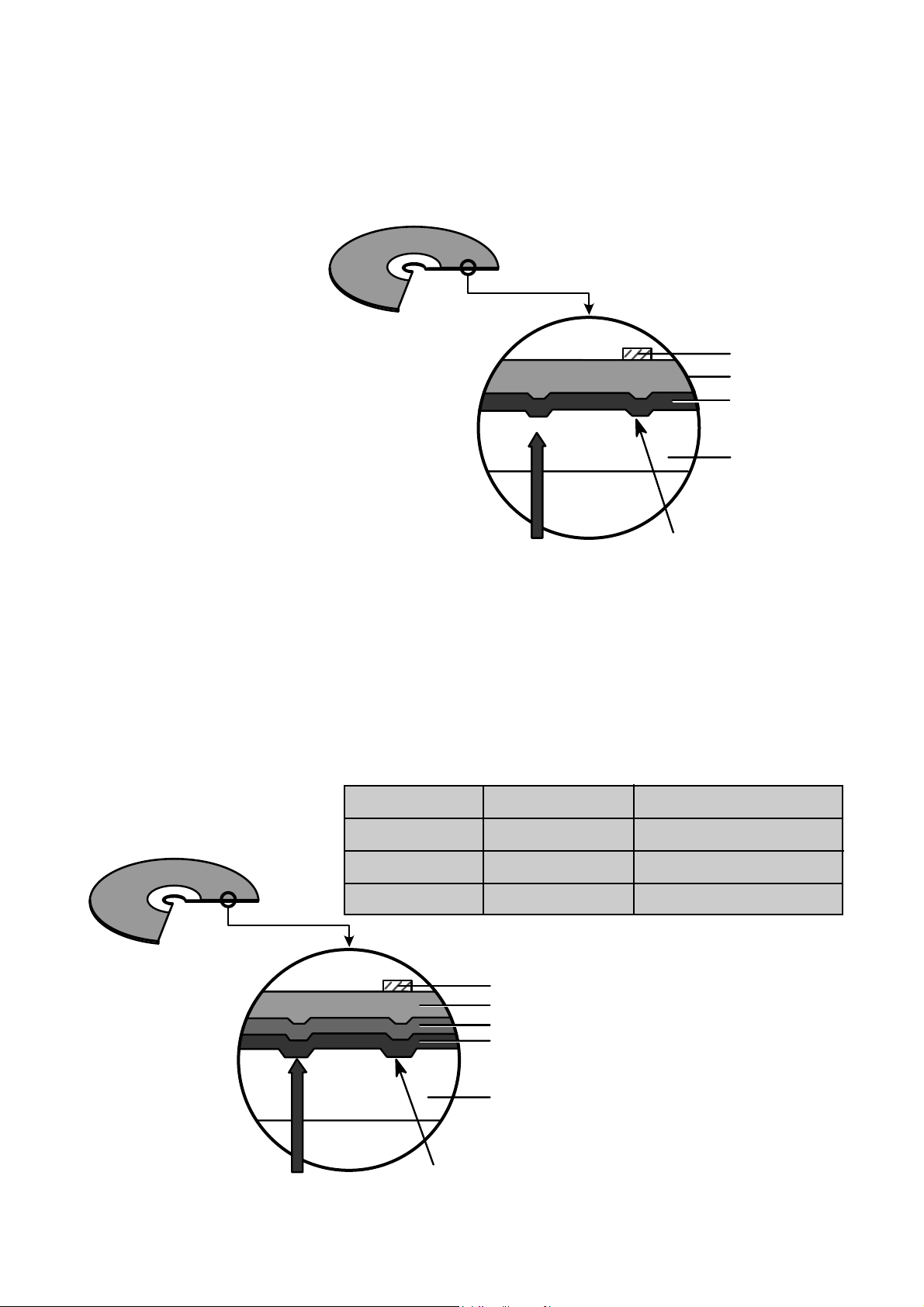
3. Disc Materials
1) CD-ROM disc
Laser Beam
Groove
Substrate
(Polycarbonate)
Organic Dye Layer
Reflective Layer
Protective Layer
Label Printing
2) CD-R disc
Pigment Reflective Layer Color
Phtalocyanine Gold/Silver Yellow/White
Cyanine Gold/Silver Dark Green/Bright Green
Azo Gold/Silver Dark Blue
• It is composed of Silver _ colored aluminum plate and Reflective layer.
• Groove (Pit) of aluminum plate make a track.
• Laser wavelength : 780 nm, Laser Power (Read): 0.5mW
• Signal is detected by the
difference of reflective beam
intensity between “pit” and
“Land” on the disc.
• It is so-called WORM (Write Once Read Many) CD.
• It is composed of polycarbonate layer, Organic dye layer, Reflective layer, and Protective
layer.Gold/Silver Reflective layer is used to enhance the reflectivity
• According to the kinds of Organic dye layer, it is divided by Green CD, Gold CD, Blue CD.
• Laser Wavelength : 780 nm, Laser Power (read) : 0.7 mW
• Recording Power : 4x(10~15mW), 8x(14~20mW), 12x(15~30mW).
• When some part of dye layer is exposed to laser heat, it’s color changs black.Therefore, writing and
reading is enabled by the difference of reflectivity between changed part and unchanged part.
• Polycarbonate layer has Pre_Groove which make a Track.
Laser Beam
Pit
Substrate
(Polycarbonate)
Reflective Layer
Protective Layer
Label Printing
Page 12
20
33)) CCDD--RRWW DDiisscc
4.
Reading process of Optical Disc
Laser Beam
Groove
Substrate
(Polycarbonate)
Reflective Layer
Dielectric Layer(TL)
Dielectric Layer(UL)
Protective Layer
Label Printing
• It is composed of polycarbonate layer, alloy(silver, arsenic) layer, aluminum reflectivity layer, protective layer.
• An crystalized alloy layer is transformed into noncrystalized by the laser heat. Therefore, writing and reading
is enabled by the difference of reflectivity.
• It is possible to overwrite about 1000 times.
• Laser Wavelength : 780 nm, Laser Power (Read) : 1.0mW
• Recording Power : Erase (4~12mW), Write (6~25mW)
• When disc rewriting, new data is overwritten previously recorded data.
• Polycarbonate layer has a Pre-Groove which make a track.
Lens
H
D
Beam
Spot
Focusing
Lens
Laser Spot
at Constant
Read Intensity
Reflected
Light
Signal
Laser Spot
Position
(Time)
Previously Recorded Marks
Groove Land Mirror
I
3
I
top
I
11
I
G
I
L
I
0
Numerical aperture: NA=nsinθ,
n: Refractive index
Focus depth : H =
λ/
NA
laser spot diameter :
D = λ/NA
2
θ
Page 13
21
5. Writing Process of CD-R Disc
a b c d e f g
a
b
c
d
e
f
g
Incident
Laser
Powe r
(Read)
(Read)
(Write)
Laser Spot
Position
(Time)
a b c d e f g
Laser Spot
Position
(Time)
Laser
Spot
Recorded
Mark
Reflected
Light
Signal
Reflected
Light
Signal
Below "ORP"– Mark Too Short
At Optimum Record Power ("ORP")
Above "ORP" – Mark Too Long
Time
6. Writing process of CD-RW Disc
Write Power
Erase Power
Read Power
Groove
Crystal
Amorphous
Amorphous
Recorded state
(lower reflectivity)
Melting/
quenching
Heating/
gradual cooling
Crystal phase
Erased state
(higher reflectivity)
Page 14
7. Organization of the PCA, PMA and Lead-in Area
1) Layout of CD-ROM disc
22
Center hole Clamping and Label Area Information Area
Lead-in Area
Lead-in Area
Diameter 15 mm
Diameter 46 mm
Diameter 120 mm
Program Area
Read Only Disc
Lead-out Area
Program Area Lead-out Area
Center hole
Clamping and Label Area
Information Area
PCA PMA
Test Area Count Area
Diameter 15 mm
Diameter 45 mm
Diameter 120 mm
Unrecorded Disc
Tsl-00:35:65 Tsl-00:15:05
Tsl-00:13:25
Tsl
99:59:74
00:00:00
in out
Test Area : for performing OPC procedures.
Count Area : to find the usable area immediately in T.A
Tsl : start time of the Lead-in Area, as encoded in ATIP
PMA : Program Memory Area
Disc Center
Disc Center
2) Layout of CD-R/RW disc
Page 15
23
8. Function of PCA and PMA area
1) PCA (Power Calibration Area)
• PCA area is used to determine the correct Laser Power for a disc.
– Method 1 : PCA area is divided by a track.
– Method 2 : The previous Calibration value is referred.
– Method 3 : ROPC is used to determine Laser Power value automatically in data writing.
• CD-R Disc can write maximum 99 Tracks but CD-RW Disc can write unlimited tracks because it has a rewritable
function.
2) PMA (Program Memory Area)
• It has a track information (track No, track Start/End time) of every track before writing completed.
– PMA area has the last written point and the next writable point of a disc.
– In case of CD to CD copy, some writer may not write PMA area.
* When Disc is Finalized,
PMA information is transferred to the Lead_In area so that general Driver can read it.
* Because PCA and PMA area exist before Lead-In area, General CD Player or CD-ROM Drive can’t read
these areas.
9. OPC and ROPC
1) OPC (Optimum Power Control)
• This is the first step of writing process, because CD writer has its own laser power value and media have different
writing characteristics,
– This is determined by the Writing characteristic, speed, temperature, and humidity.
– Laser wavelength is determined by the environmental temperature (775~795nm) and Optical Laser Power is
determined by the test and retry.
• Asymmetry and optimum writing Power
– EFM signal Asymmetry is determined by the writing power.
Therefore, Optical Power which has the same value to the preset power value can be estimated by measuring
HF signal Asymmetry on the PCA area.
• Measurement of Asymmetry
* Parameter setting (Beta) : Using AC coupled HF signal before equalization
Beta = (A1+A2)/(A1-A2)
Time
P << Po
Time
P = Po
HF Signal
A1
0
A2
Time
P >> Po
Page 16

2) ROPC (Running Optimum Power Control)
• Variable primary factor of Optimum Power
– Change of Power sensitivity on the Disc. (limited to 0.05 *Po)
– Wavelength shift of the laser diode due to the operating temperature change.
– Change of the Spot aberration due to the Disc skew,
Substrate thickness, Defocus.
– Change of Disc or Optics conditions due to the long term OPC
==> It is necessary to adjust continuously to obtain the Optimum Power.
• Principle of Running OPC
– To meet the factors mentioned above,
a horizontal _ direction movement of a curve is uesd.
– Beta = f(B-level) = constant on the Recorded Disc
– Procedure of ROPC
a. Reference B-level is determined during OPC Procedure.
b. During Recording, B-level value is controlled to have a close
Reference B-level value.
c. Normalization of B-level is used to eliminate the effect of reflectivity fluctuation.
==> The reflected B-level value is normalized by the disc reflectivity itself.
24
CCDD--RR//RRWW
Media
Write Strategy
Determination
PCA Test Area
Program Area
PMA Area
Lead-In Area
Lead-out Area
OPC
PCA Count Area
ROPC
* Recording Capacity of CD-R/RW (74Minute Recording media)
• (2048 Byte/Sector) X (75 Sector/Second) X (60 Second/Minute) X 74 Minute
= 681,984,000 Bytes = 682 Mbytes
• But the actual recording capacity is about 650 Mbytes. (according to the ISO 9660 standard, approximately
30 Mbytes are used to make directory structure and volume names.)
Incident recording pulse
Reflected recording pulse
Sampled timing B
11T
Sample B-level (Write Power)
Level B
Sampled at timing B
Pwo decided by OPC
Recording Power
Level B with Pwo
normalized to recording power
Sample Disc Reflectivity
(Read power)
10. Writing Process of DISC
Page 17

INTERNAL STRUCTURE OF THE PICK-UP
1. Block Diagram of the PICK-UP
25
CN09 Vcc-PD
CN10 Vc-PD
CN11 GND-PD
CN01 A
CN02 B
CN08 C
CN07 D
CN05 F
CN03 G
CN06 H
CN27 OUT-FMD
CN04 E
CN34 GND-FMD
CN33 Vc-FMD
CN32 Vcc-FMD
CN28 F+
CN31 F-
CN30 T+
CN29 T-
CN25 IINR
CN24 IIN2
CN23 IIN3
CN22 IIN4
CN17 OUTENR
CN18 OUTEN2
CN19 OUTEN3
CN20 OUTEN4
CN21 GND-LD1
CN16 GND-LD2
CN12 Vcc-LD
CN15 RAMP
CN14 ENABLE
CN13 OSCEN
CN26 TMP
TRACKING
LD drive IC
GND
GND
GND
GND
Vcc
IINR
IIN2
RFREQ
OUTENR
OUTEN2
OUTEN3
OUTEN4
IIN3
IIN4
Vcc
Vcc
Vcc
IOUT
IOUT
RAMP
ENABLE
OSCEN
GND
GND
LASER DIODE
THERMISTOR
FOCUS
Actuator
Front monitor diode
Vcc ADJ
OUT
RV
2P
4.7k
Vref
GN
8-divided photo diode
SF-W03PDX
20k
50
20k
50
20k
50
20k
50
50k
10
50k
10
50k
0.1
10k
4.3k
1.5k
Chip ferrite beads
LL560 equivalent
10
50k
10
1.5k
1.5k
1.5k
Page 18
2. Pin Description
26
Pin No. Symbol I/O Function
1 A O PDIC A OUT
2 B O PDIC B OUT
3 G O PDIC G OUT
4 E O PDIC E OUT
5F
O
PDIC F OUT
6H
O
PDIC H OUT
7 D O PDIC D OUT
8 C O PDIC C OUT
9 VCC-PD I PDIC VCC
10 VC-PD I PDIC VC
11 GND-PD
_
PDIC GND
12 VCC-LD
_
LDIC VCC
13 OSCEN I Module Control SW L:off, H:on
14 ENABLE I LD Drive Current OFF SW, L:LD off
15 RAMP I RAMP
16 GND-LD2
_
LDIC GND
17 OUTENR I OUT ENABLE
18 OUTEN2 I Write Enable 1L : Write 1 ON
19 OUTEN3 I Write Enable 2L : Write 2 ON
20 OUTEN4 I Write Enable 3L : Write 3 ON
21 GND-LD1
_
LDIC GND
22 IIN4 I Overdrive Analog Control Voltage Input
23 IIN3 I Overdrive Analog Control Voltage Input
24 IIN2
I
Overdrive Analog Control Voltage Input
25 IINR I Real Power Analog Control Voltage Input
26 TMP O THERMISTOR
27 OUT-FMD O FMD-IC
28 F+
I
Focus coil+
29 T- I Tracking coil-
30 T+ I Tracking coil+
31 F- I Focus coil-
32 VCC-FMD I FMDIC VCC
33 VC-FMD I FMDIC VC
34 GND-FMD
_
FMDIC GND
Page 19
3. Signal detection of the P/U
1) Focus Error Signal ==> (A+C)-(B+D)
This signal is generated in RF IC (IC401 : OTI-9071) and controls the pick-up’s up and down to focus on
Disc.
2) Tracking Error Signal (DPP Method) ==> {(A+D)-(B+C)}- kx {(F+H)-(E+G)}
This signal is generated in RF IC (IC401 : OTI-9071) and controls the pick-up’s left and right shift to find
to track on Disc.
3) RF Signal ==> (A+B+C+D)
This signal is converted to DATA signal in DSP IC (IC101 : OTI-9795).
27
Pick-Up module
Photo Diode
Tracking
Focusing
Infrared Iaser
k[(F+H) - (E+G)]
(A+D) - (B+C)
(A+D) - (B+C) - k[(F+H) - (E+G)]
Offset
TE
Tp
Sub2
Main
Tp/2
Sub1
Track Center
F, E
D,C
A,B
H,G
Page 20

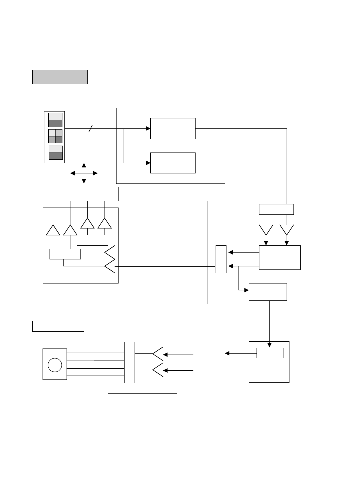
DESCRIPTION OF CIRCUIT
1. ALPC (Automatic Laser Power Control) Circuit
1-1. ALPC Loop Circuit
28
4
2
3
50
51
60
11
13
12
10
9
6
5
7
8
FPDO
FPDI
x10
FVREF
RFPDSH
WF
PDSH
WL
DON
VRDCN
WLDON
VRDC1
VRDC
H
H
H
H
H
-8 to 7.5dB
0.5dB/step
S/H
H
H
8
8
8
5K
-1
5K
rldon
rdaon
readlev1
readlev2
fgdg
ivon
wdaon
vwdcsw1, vwdcsw2
writelev
rwapc
RREF
VWDCN
VW DC
WREF
VWDC1
VWDC2
7
RFPDSH
4
WFPDSH
IC402
3.3V
C411
IC401 OTI 9071
C411
R444
Vref
C427
R442
R420R421
IC404
BU4053
5 4
R434
IC403
DAC
3
4
R404
R403
7
R423
18
R415
R414
19 23
IC101 OTI 9795
166
WG ATE
3
5
2
181
RESAM P1ROPC1
186
19
20
14
EFM1
EFM2
183
184
141
LDON
27
33
25
24
VWDC2
C412
R414
C412
13
D402
2
C425
IC361
74VHC157MTC
CN401
P/U
VW DC
VRDC
FVREF
FPDO
C499
S/H
-1
10
5
x10
Page 21

1-2. ALPC(Automatic Laser Power Control) Circuit Operation
This circuit consists of Feedback Loop to maintain light output of the Laser Diode(FPDO).
Feedback signal, output voltage from PD(Photo Detector) of P/U, is used monitor the light power of
Laser Diode.
1) Read Loop
RREF(Read Reference Voltage) of IC401(OTI-9071) Pin 10, which is from DAC(IC403) Pin 18, is the
reference level of the Read Loop part of this ALPC Circuit.
• When Playback
VRDC(Pin 12) signal of IC401(OTI-9071) is output to P/U through Gain Control S/W and drives Laser
Diode during play back.
This S/W Ciruit is designed to reduce transition time from CD-RW writing mode to playback mode.
• When writing mode
- CD-R
Three Laser Power Levels, Read, Write, and Overwrite, are used to write on CD-R disc, and Read
Level is used to monitor the output laser power.
For stabilizing read loop, the S/H signal(RFPDSH), which sample and hold the Read Level of laser
power in the CD-R writing mode, is input through Pin 50 of OTI-9071.
- CD-RW
Three Laser Power Levels, Read, Erase and Write, are used to write on CD-RW disc, and Erase
Level is used, during CD-RW writing, to monitor output laser power.
It is not VRDC but VWDC that is the output signal of the control loop performed by Erase level.
2) Write Loop
For stabilizing write Loop, the S/H signal(WFPDSH), which sample and hold the Erase Level of laser
power in the CD-RW writing mode, is input through Pin 51 of OTI-9071.
Output voltage of Write Loop, VWDC(Pin 6 of OTI-9071), is protected by the high limit diode applied to
P/U.
In the writng mode, the reference signal of Write Loop is WREF(Pin 3&4 of IC403)and it is input to Pin 5
of IC401(OTI-9071).
29
Page 22

2. RF Amplifier Circuit
Block Diagram
30
off set adj
(A+C)-(B+D)
Gain Adj
LPF
(100KHz)
LPF
(80KHz)
FE
30
IC101 197
A,B,C,D
91 92 93
94
Offset adj
18
CEO
IC101 204
LPF
(200KHz)
LPF
(200KHz)
E,F,G,H
96 97 98
99
Gain Adj
LPF
(80KHz)
28
+
-
IC101
198
TEBC
IC101
194
LPF
(200KHz)
Gain Adj
HPF
HPF
33
34
EQRFP
EQRFN
IC400
IC101
163
(10KHz)
K
BPF AGC
41
AGC
Slice
Circuit
ATFG
IC201
132
OTI-9071
PDIC
VC
GND
VCC
Pick up SF-WO3PDX
32
+
-
OTI-9795
Page 23
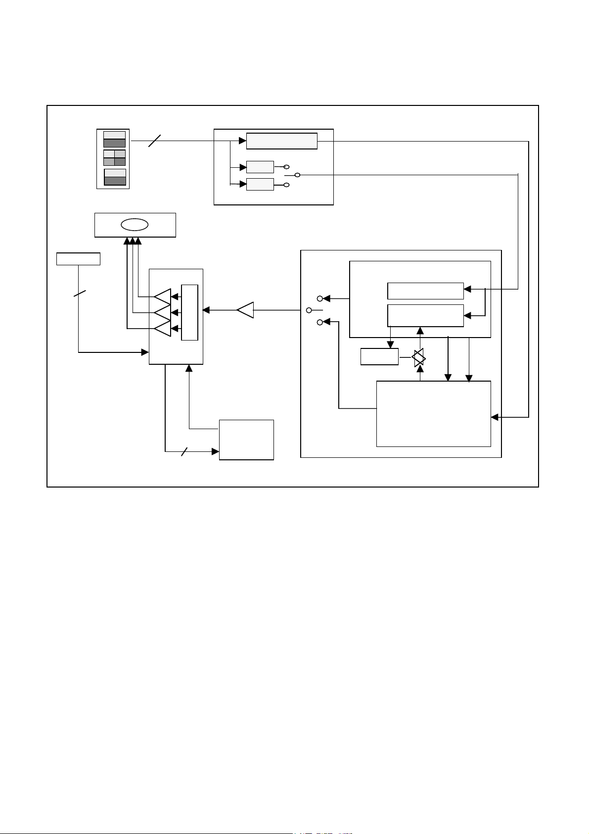
3. Focus/Tracking/Sled Servo Circuit
3-1. Focus, Tracking & Sled Servo Process
31
Focus, Tracking Servo
C
B
D
A
E
F
G
H
Pick- up
A,B,C,D,E,F,G,H
A,B,C,D
Focus Error
Detector
Track Error
Detector
A,B,C,D
E,F,G,H
IC401 OTI9071
FE
TE
TE FE
A/D
Low freq Gain Filter
Digital
EQ
DAC
Sled Co ntrol
Signal
IC101
Servo Control
OTI9795
LEVEL SHIFT
LEVEL SHIFT
Tracking Focus ing
Actuator
FAO
TAO
F+
F-
T+
T-
IC201
u-COM
Sled Co ntrol
M
SLED MOTOR
SLO
LEVEL SHIFT
SM_A-
IC501
M56788AFP
SM_A+
SM_B+
SM_B -
IC403
BU2500FV
(DAC)
A/D
IC501 M56788AFP
Page 24

3-2. Focus Servo
The aim of Focus Servo is to maintain the distance between object lens of P/U and disc surface, so that
the detected RF signals (A, B, C, D) can be maximized.
Focus Servo is based on focus error (FE) signal which is generated from focus error detection block in
OTI9071 (IC401) using Astigmatism Method. Focus gain and path can be changed at the OTI9071
according to the disc, and the resulting output (FE) is input to Servo IC (IC101, OTI-9795).
FE signal after first amplification in OTI-9795 is A/D converted and input to Digital Equalizer Block, most
important part at the Focus Servo. At the Digital Equalizer, adjustments for Focus Bias and Loop Gain are
performed.
After D/A converted, Focus servo signal is output through FOO port (OTI-9795, Pin 207) and drive Focus
Actuator through the Focus Drive IC (IC501, M56788AFP).
3-3. Tracking Servo
The aim of Tracking Servo is to make laser beam trace the data track on disc. Tracking Error (TE) signal
is generated from tracking error detection block in OTI9071 (IC401) using DPP (Differential Push-Pull)
Method. DPP method uses not only main beam (A, B, C, D) but side beams (E,F and G, H) for correcting
DC offset generated in Push-Pull method.
The remaining procedures of TE signal processing in OTI-9795 is similar to Focus Servo.
After D/A converted, Tracking servo signal is output through TRO port (OTI-9795, Pin 208) and drive
Tracking Actuator through the Tracking Drive IC (IC501, M56788AFP).
3-4. Sled Servo
The working distance of tracking actuator is too short to cover whole disc radius. Sled Servo make PU
move by little and little so that the laser beam keep tracing the data track on disc continuously when
tracking actuator reaches the working limit.
Another function of Sled Servo is to seek a target point on disc, following user commands.
Sled control signal, STEP-CTRL0,1 from BU2500FV is generated in µ-com. STEP-CTRL0,1 are output to
sled motor via IC501 (M56788AFP).
32
Page 25
4. Spindle Servo Circuit
4-1. Spindle Servo Process
4-2. Spindle Servo
Spindle servo is as followings;
1) Wobble CLV x2, x4, x8, x12 : Blank area in CD-R, CD-RW.
2) CD 15x CAV: Eccentric CD-R/RW.
3) CD 20x CAV: Video CD, CD-DA in CD-ROM/R
4) CD 24x CAV: Recorded area in CD-RW.
5) CD 32x CAV: CD-ROM. Recorded area in CD-R.
– Spindle Servo is controlled by IC101 (OTI-9795) and servo signal is output via DMO (pin 2).
33
C
B
DA
E
F
G
H
Pick- up
IC401 OTI9071A
Wobble Signal
Generator
RF
SRF
EFM
WBLIN
Decode P LL
Frequency
Controller
CD-DSP/S ERVO
LOCK
DEFS
MOTOR SPEED
CONTROLLER
FILTER
TON
DMO
ATIP CLV, FG
Level Shift
Hall Sensor
M
Spindl e Motor
IC 201
u-COM
SPNON
SPNFG
REVDEF
IC101 OTI9795
CD EFM CLV
CAV x32
6
8
IC510 BA6664FM
Page 26

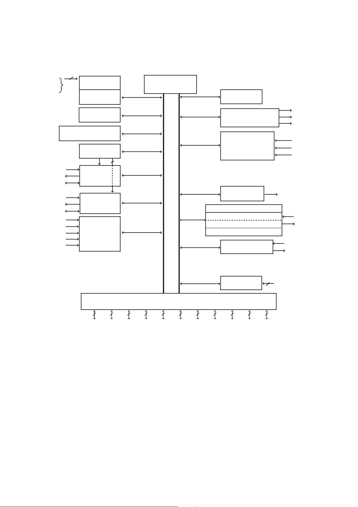
MAJOR IC INTERNAL BLOCK DIAGRAM AND PIN DESCRIPTION
IC401 (OTI-9071) : RF Signal Processor for CD-R/RW
Block Diagram
34
CEO
MPPO
CEP
CEN
BS
TEIN
TE
FE
TC
XTAND
AGCCAP1
SADO
FEO
MPPO
SPPO
VREF
SBCO
VREF
MCLK
TE
BHO1
VREF
SWRF1
SWRF2
WLDON
VREF
VREF
SRFO
RFO
PHO1
AGCCAP2
AGCCAP3
AGCON
ATFM
ATFG
BPFCLK
SRCH#
SRCHLP
DTE
RPBC
RRFIN1
TEBC
RP
RX
TX
BHO1
PHO1
PHO2
RECD1
RECD2
RRF
EQRFP
EQRFN
AUX1
VARIOUS
INTERNAL
SIGNAL
AUX2
AUX3
WREF
MUXOUT1
MUXOUT2
BHO2
BHC1
PHC1
VWDC1
VWDC2
VREF
2VREF
RBIAS
FVREF
FPDO
FPDI
RFPDSH
WFPDSH
VRDCN
VRDC
RREF
VWDCN
VWDC
MCLK
PRST#
ULAT
UTXD
URXD
USCK
WREFSH
WPLTSH
GAINUP
WBLSH
HIN
GIN
FIN
EIN
SPDSH
DIN
CIN
BIN
AIN
MPDSH
HAVC
BHC2
PHC2
RRFIN2
WLDON
RECDIN
INPUT
S/H
STAGES
AND
MATRIX
FUNCTIONS
FOCUS
AND
TRACKING
FUNCTIONS
ATIP
FUNCTIONS
RP
TX/RX
GENERATION
PEAK
BOTTOM
HOLD
PEAK
BOTTOM
HOLD
FOR BETA
RF
EQUALIZER
APC
VREF
uC
I/F
Page 27

35
• Pin Assignment
Pin No. Name Analog Digital Pin Description
Type Type
1 AVDD P Analog power
2 FPDI I Laser power monitor output
3 FVREF I APC reference voltage
4 FPDO O Laser power monitor output
5 WREF I/O Power setting input/output voltage for write APC
6 VWDC O Laser driver control output for write.
7 VWDC1 O Auxiliary laser driver control output for write.
8 VWDC2 O Auxiliary laser driver control output for write.
9 VWDCN I/O Laser driver control input for write.
10 RREF I/O Power setting input/output voltage for read APC
11 VRDCN I/O Laser driver control input for read.
12 VRDC O Laser driver control output for read.
13 VRDC1 O Laser driver control output for CDRW read
14 RBIAS I/O Reference current setting pin
15 AVSS G Analog ground
16 2VREF I/O 2x Reference voltage (4.2V)
17 AVDD P Analog power
18 CEO O Center position signal
19 CEP I/O Gain and fc setting node for center position signal
20 CEN I/O Gain and fc setting node for center position signal
21 RP1 O RF ripple signal
22 RPBC I Ripple balance
23 RPCT I Ripple center input
24 RP2 O RF ripple signal
25 RPIN I AC-coupled RP input
26 RPDC O DC-coupled RP signal output
27 BS O Beam strength
28 TE O Tracking Error output
29 TEIN I External bypass TE input
30 FE O Focus error output
31 VREF I/O Reference voltage (2.1V)
32 TEBC I Tracking Error Balance
33 EQRFP O Equalized RF output (+ve)
34 EQRFN O Equalized RF output (-ve)
35 AGCCAP1 I/O AGC1 gain control node
36 AGCCAP2 I/O AGC2 gain control node
37 AGCCAP3 I/O AGC3 gain control node
38 AVDD1 P Analog power
39 ATFM O Wobble signal output
40 AVSS G Analog ground
41 ATFG O Digital wobble signal output.
42 BPFCLK I ATIP band-pass filter clock input.
Page 28
36
Pin No. Name Analog Digital Pin Description
Type Type
43 TC O Track crossing signal
44 DVDD P Digital power
45 TX O Zero crossing of TE
46 DVSS G Digital ground
47 RX O Zero crossing of RP
48 WPLTSH I SWRF1 sample gate
49 WREFSH I SWRF2 sample gate
50 RFPDSH I Sample pulse for read APC
51 WFPDSH I Sample pulse for write APC
52 MPDSH I Main beam input sample gate
53 WBLSH I Wobble signal sample gate
54 SPDSH I Side beam input sample gate
55 DVDD P Digital power
56 AGCON I ATIP AGC on
57 DVSS G Digital ground
58 GAINUP I Gainup photodetector signals
59 XTAND O Off-track detection output
60 WLDON I Write laser on
61 RECD1 O Recording area detection
62 RECD2 O Recording area detection
63 ULAT I Microcontroller latch
64 DVDD P Digital power
65 USCK I Microcontroller clock
66 UTXD O Microcontroller transmit data
67 URXD I Microcontroller receive data
68 DVSS G Digital ground
69 PRST# I Power-on-reset (active low)
70 MCLK I 34.5744MHz Clock Input
71 AVSS G Analog ground
72 AUX1 I Auxiliary analog input for MUXOUT
73 AUX2 I Auxiliary analog input for MUXOUT
74 AUX3 I Auxiliary analog input for MUXOUT
75 MUXOUT2 O Analog multiplexer output 2
76 MUXOUT1 O Analog multiplexer output 1
77 PHO1 O Peak hold output 1
78 BHO1 O Bottom hold output 1
79 PHC1 I/O Peak hold control node
80 BHC1 I/O Bottom hold control node
81 PHO2 O Peak hold output 2
82 BHO2 O Bottom hold output 2
83 PHC2 I/O Peak hold control node
84 BHC2 I/O Bottom hold control node
85 RRFIN2 I RRF input pin for peak/bottom hold 2
Page 29
37
Pin No. Name Analog Digital Pin Description
Type Type
86 RRFIN1 I RRF input pin for peak/bottom hold 1
87 RECDIN I RF input for recording area detection
88 AVDD P Analog power
89 RRF O Read RF signal output
90 AVSS G Analog ground
91 AIN I Main beam input signal (A)
92 BIN I Main beam input signal (B)
93 CIN I Main beam input signal (C)
94 DIN I Main beam input signal (D)
95 HAVC I/O Main/Side beam input signal reference voltage
96 EIN I Side beam input signal (E)
97 FIN I Side beam input signal (F)
98 GIN I Side beam input signal (G)
99 HIN I Side beam input signal (H)
100 AVSS G Analog ground
Page 30
IC101(OTI-9795) : ATAPI Interface, Write and DSP Signal Processor
Block Diagram
38
PANICIN
ESFS
EEFS
WGATE
HFSW
EFM1 3
WRSMP
EFCK
EFMNT1-4
E11TP
E11TS
RESMP1,2
ROPC1 3
MONIT0
MONIT
EFMR3
EFMR2
EFMR1
EFM
ASY
MIO0/SDATA
MIO1/ALRCK
MIO2/ABCK
DOUT
MIO3/EMPH
L
R
WBLIN
XIN
XOUT
C34M
CLKOUT
MON
FGIN
SBRK
REVDET
SLO
FOO
TRO
TC
VREF
2VREF
FE
TEBC
BS
TE
RPBC
RP
RXTXCE
LDON
FLAGA D
DMO
PRST#
UAD[7:0]
UALE
UA[15:0]
URDY
UWR#
URD#
UCS0#
UCS1#
UINT0#
UINT1#
SDINT1#
RSC#
RCLKE
RCLK
RD[15:0]
ROE#/LDQM
RCASL#
RCASH#/UDQM
RWE#
RRAS#
RAD[12:0]
HDASP#
HA[2:0]
HPDIAG#
IOCS16#
HIRQ
DMACK#
HIORDY
HRD#
HWR#
HDRQ
HD[15:0]
HRST#
CS3FX#
CS1FX#
DPLL
C1/C2
Decoder
VPSET
Register
CIRC
CIRC
4K SRAM
4K SRAM
C1/C2
Encoder
PLL
Audio
ATIP
Demodulator
CLK
Generator
Spindle
Motor
Controller
ASYNC
TON Bit
ASYNC+
MSF
DMCON Bit
0 1
CD-SERVO
Spindle/Focus/Tracking/Sled
Microcontroller
Interface
USB
D+
D-
48MHz
ATAPI/
SCSI
DMA
Interface
RAM
Interface
C3 Encoder
Sector
Processor
Encoder
Buffer
Manager
Decoder
Buffer
Manager
NXSYNC Bit
nX-1X
1X/2X CLV
34.5744MHz
Data
Decoder
Subcode
Encoder
Data
Decoder
Subcode
Interface
C3
Decoder
0
1
NX-1X
Audio
Processor
OTI-9795
Page 31

• Pin Description
The following pin descriptions and assignments are grouped by function, in reference to their related interface.
Pin names ending with # signify active LOW signals. Pin names not ending with # signify active HIGH signals
39
Pin No. Pin Name Type
Description
137 XIN
_
Crystal In : System Clock
136 XOUT
_
Crystal Out: System Clock
138 CLKOUT/ O Clock Output
ATIPCK ATIPCK : Externa Write Strategy
6 C34M I/O Clock out : Set to 34.5744MHz
CD ENCODER Interface
PPiinn NNoo.. PPiinn NNaammee TTyyppee
Description
168 PANICIN I
S
Panic Input
132 WBLIN I
S
Wobble In : Wobble Input–Digital Signal
167 HFSW O High Frequency Modulation Switch
166 WGATE O Write Gate
180 WRSMP O Write Level Sample : Sample hold signal of write levels on reading
183 EFM1 O EFM 1 : EFM output
184 EFM2 O EFM 2 : EFM output
185 EFM3 O EFM 3 : EFM output
169
EFMNT1/ EFMNT1 : EFM pit pattern length indicator/
EMFNRZ
O
EFMNRZ : EFM Signal Output
170
EFMNT2/ EFMNT2 : EFM pit pattern length indicator/
69M
O
69M : 69.1488MHz
171 EFMNT O EFMNT3 : EFM pit pattern length indicator
172 EFMNT4 O EFMNT4 : EFM pit pattern length indicator
175 E11TP O EFM11T Pit Pattern : EFM11T Pit pattern indicator
176 E11TS O EFM11T Space Pattern : EFM11T space pattern indicator
177 EFCK O EFM Bit Clock : EFM bit Clock generated from internal clock in CD encoder
181 RESMP1 O Read Level Sample1 : Sample hold signal of read levels on writing
182 RESMP2 O Read Level Sample2 : Sample hold signal of read levels on writing
186 ROPC1 O
Running OPC1 : Sample hold signal 1 of reflected beam for running OPC
187 ROPC2 O
Running OPC2 : Sample hold signal 2 of reflected beam for running OPC
188 ROPC3 O
Running OPC3 : Sample hold signal 3 of reflected beam for running OPC
Clock
WOBBLE Motor Interface
Pin No. Pin Name Type
Description
4 REVDET I
S
Reverse Detect Motor Drive : Indicates spindle motor is rotating in reverse direction
5FG ISFG IN : HG (tachometer) pulse input
7 MON O Motor Drive On : Enables spindle motor drive
8 SBRK O Short Brake : Stops spindle motor by applying a short pulse to the motor winding
Page 32

40
WOBBLE Motor Interface
CD-SERVO Interface
Pin No. Pin Name Type
Description
140 MONIT0 O Monitor 0 : Test pin
DEFAULT-Wobble Clock
179 EEFS O EFM Frame Sync
178 ESFS O Encoder Subcode Frame Sync
CD-DSP PIN
Pin No. Pin Name Type
Description
163 EFM I
A
EFM Analog Data
162 ASY O
A
Asymmetry DAC Output
159 EFMR1 I
A
EFM Analog Data Bias 1
160 EFMR2 I
A
EFM Analog Data Bias 2
161 EFMR3 I
A
EFM Analog Data Bias 3
133 MONIT/ O
CD-DSP Monitor Output : MONIT is used to output several internal CD-DSP signals
PLCK Bit Clock : External Write Strategy
Pin No. Pin Name Type
Description
2 DMO O
A
Spindle Motor Servo Output
3 SLO O
A
Sled Servo Output
207 FOO O
A
Focus Servo Output : Focus servo feedback signal
208 TRO O
A
Tracking Servo Output : Tracking servo feedback signal
194 TEBC O
A
Tracking Error Balance Control
197 FE I
A
Focus Error
198 TE I
A
Tracking Error
201 BS I
A
Beam Strength
202 RPBC O
A
Ripple Balance Control
203 RP I
A
Ripple of RF
191 RX I
S
RP Zero Crossing : Used for fine search
192 TX I
S
TE Zero Crossing : Track crossing signal input used in conjunction with RX to
perform fine searches
204 CE I
A
Center Position Error
141 LDON O Laser Diode On
193 TC I
S
Track Count Input : High-frequency track crossing signal input used to perfrom
rough searches and to increment the internal track counter.
142 FLAGA O Servo Monitor Flag A : FLAGA is used to output one of four internal servo
signals. FLAGA can also be used as a general output port.
145 FLAGB O Servo Monitor Flag B : FLAGB is used to output one of four internal servo
signals. FLAGB can also be used as a general output port.
146 FLAGC O Servo Monitor Flag C : FLAGC is used to output one of four internal servo
signals. FLAGC can also be used as a general output port.
149 FLAGD O Servo Monitor Flag D : FLAGD is used to output one of three internal servo
signals. FLAGD can also be used as a general output port.
Page 33

41
AUDIO Interface
Pin No. Pin Name Type
Description
143 MIO0/L- I/O Multiple I/O 0 : MIO0 is used to output several internal test signals.
DEFAULT-Serial Data : This signals is for 16-bit PCM serial audio data. It can be
used to send audio data to an external or internal OTI-9795 DAC. Audio data is in
24-bit slot format for input and output.
CD-DSP Error Flag : External Write Strategy
L- : Differential Audio Output
144 MIO1/L+ O Multiple I/O 1 : MIO1 is used to output several internal test signals.
DEFAULT-Audio Left/Right Clock : Indicates the start of the 24-bit value on
SDATA. High indicates the start of the left channel.
CD-DSP Error Flag Clock : External Write Strategy
L+ : Differential Audio Output
147 MIO2/R+ O Multiple I/O 2 : MIO2 is used to output several internal test signals.
DEFAULT-Audio bit Clock : This is the data bit clock output for SDATA.
There are 24 cycles of bit clock for each 16-bit audio word.
Read Frame Clock : External Write Strategy
R+: Differential Audio Output
139 DOUT O
Digital Audio Output : Bi-phase serial audio output that follows the EIAJ CP1201 standard.
148 MIO3/R- O Multiple I/O 3 : MIO3 is used to output several internal test signals.
DEFAULT-De-Emphasis Control
C1* : External Write Strategy
R- : Differential Audio Output
151 L O
A
Left Channel Audio Output
154 R O
A
Right Channel Audio Output
ATAPI /SCSI Pass-Through/USB Host Interface
Pin No. Pin Name Type
Description
76 HD15
78 HD14
80 HD13
82 HD12
86 HD11
88 HD10
90 HD9
94 HD8
95 HD7
91 HD6
89 HD5
87 HD4
85 HD3
81 HD2
79 HD1
77 HD0
HD15-8
&HD6-0
=I/O PUB
HD7=
I/O PUB
or I/O
Host Data Bus (ATAPI & SCSI DMA Mode) : If RD14/HD7PUEN is pulled LOW
during power-on or host reset, the internal pull-up resistor on HD7 will be
disabled. If HD7PUEN is pulled HIGH after power-on or host reset, the internal
pull-up resistor on HD7 will be enabled. The pull-up reistor may also be disabled
by setting RMDHD7PU (0B0h.7)=1.
The host interface supports ATA/ATAPI, SCSI pass-through, or USB transfer protocols. ATAPI Mode, which is compatible with
the ATA/ATAPI-4 specification, is enabled when bit SCSIEN (07Bh.0) = 0 and bit USBENBL (0A7h.0) = 0. SCSI Pass-Through
Mode, which is compatible with the Symbios 53CF94/6 Fast SCSI Controller, is enabled when SCSIEN - 1 and USBENBL =0.
Universal Serial Bus Mode, which is compatible with the USB 1.1 specification, is enabled when SCSIEN =0 and USBENBL
=1. Signal IFSEL also controls the SCSIEN setting. In ATAPI Mode, PIO, DMA, and Ultra DMA transfers are selected by bits
SDMAb (01Fh.2) and SUDMA (0C3h.7).
Page 34

42
Pin No. Pin Name Type
Description
ATA Write Strobe (ATAPI Mode) : During PIO and DMA transfers, the host uses
this signal to write data to the device.
ATA Stop Ultra DMA Burst (ATAPI Mode): During Ultra DMA transfers, the host
uses this signal to halt a burst transfer. Bit SUDMA (0C3h. 7) enable UDMA mode.
SCSI DMA Write Strobe (SCSI DMA Mode): The SCSI protocol controller latches
data from the OTI-9795 on the rising edge of DBWR#, which is driven by the OTI9795 and drives its timing from the SCSICLK signal.
ATA Read Strobe (ATAPI Mode) : During PIO and DMA transfers, the host uses
this signal to read data from the device.
ATA Ultra DMA Host Ready/Host Data Strobe (ATAPI Mode) : The host uses
this signal to indicate it is ready to begin an Ultra DMA read data tranfer. During an
Ultra DMA write tranfer, the host uses this signal to strobe data to the device.
SCSI DMA Read Strobe (SCSI DMA Mode) : The OTI-9795 latches data from the
SCSI protocol controller on the rising edge of DBRD#, Which is driven by the OTI9797 and derives its timing from the SCSICLK signal.
ATA Address 2-1 (ATAPI Mode) : The Host uses the 3-bit ATA address to
select an ATAPI control command block register or data port.
ATA Address 0 (ATAPI Mode): The host uses the 3-bit ATA address to select an
ATAPI control command block register or data port.
48MHz USB Reference Clock (USB Mode) : If bit USBCKSEL (0A9h.2) = 1, 48M
is used as the USB reference clock input, and a 48MHz clock signal must be input
to 48M. If USBCKSEL=1, the internal CD-Decoder system clock (controlled by bits
PLLCO1-0 [2FEh-2FDh]) is used, and 48M must be grounded.
ATA I/O Chip Select 16 (ATAPI Mode) : For PIO transfer, IOCS16# indicates to
the host system that the 16-bit data port has been addressed and the chip is
prepared to send or receive a 16-bit data word.
ATA Chip Select 1 (ATAPI Mode) : The host uses this signal to select the ATAPI
command block registers for access.
USB Differential Serial Data - Negative (USB Mode)
ATA Chip Select 3 (ATAPI Mode) : The host uses this signal to select the ATAPI
control block registers for access.
SCSI Reference Clock (SCSI DMA Mode) : If bit SCSICLKS (07Bh.6) = 0, this
signal is used as the SCSI DMA reference clock (40MHz is recommended). If
SCSICLKS = 1, the internal CD-Decoder system clock (controlled by bits PLLCO10 [2FEh-2FDh]) is used, and this signal must be grounded.
USB Differential Serial Data - Positive (USB Mode)
ATA DMA Request (ATAPI Mode) : This signal will be asserted for DMA data
transfer when the chip is ready to transfer data to or from the host. This signal is
used in a handshake manner with DMACK#.
SCSI DMA Request (SCSI DMA Mode) : The SCSI protocol controller uses
DREQ to request data transfer with the OTI-9795.
ATA DMA Acknowledge (ATAPI Mode) : This signal is used by the host to
respond to HDRQ.
SCSI DMA Acknowledge (SCSI DMA Mode) : The OTI-9795 uses DACK# to
acknowledge it is ready for data transfer.
HWR#/
STOP/
DBWR#
I
PU
O
72
HRD#/
HDMARDY#/
HSTROBE
DBRD#
IPU
O
71
61
64
62
66
59
58
HA2/
HA1
HA0/
48M
IOCS16#
CS1FX#/
USBD-
CS3FX#/
SCSICLK/
USBD-
I
S
I
S
I
S
I
S
O
OD
73
69
HDRQ/
DREQ
DMACk#/
DACK
I
PU
I
PU
O
O
Page 35

43
Pin No. Pin Name Type
Description
ATA Interrupt Request (ATAPI Mode) : This signal is used to interrupt the host
system. HIRQ is controlled by bit HINTRQ (02Eh.3).
SCSI Interrupt (SCSI DMA Mode) : This signal is asserted by the SCSI Protocol
Controller to interrupt the system controller. DTE (0E3h.2) is set to 1 when SIRQ#
is asserted.
ATA I/O Ready (ATAPI Mode) : When PIO mode is active, the device deasserts
this signal to extend any host read data access cycle when the host FIFO is empty
or EDAC throtting is enabled.
ATA Ultra DMA Device Ready / Data Strobe (ATAPI Mode) : The device uses
this signal to indicate it is ready to begin an Ultra DMA write data transfer. During a
read transfer, the device uses this signal to strobe data to the host.
ATA Drvie Active/Drive 1 Present (ATAPI Mode) : This is a time-multiplexed
signal that indicates if a drive is active or Drive 1 is present. HDASP# is controlled
by bit DASPEN (020h.5). Firmware can read the state of HDASP# from bit DASPb
(02Eh.0).
ATA Passed Diagnostics (ATAPI Mode) : This signal is asserted by Drive 1 to
indicate to Drive 0 that it has completed diagnostics. HPDIAG# is controlled by bit
PDIAGEN (020h.6). Firmware can read the state of HPDIAG# from bit PDIAGb
(02Eh.1).
55 HRST# I
S
Host Reset : The host uses this signal to reset the OTI-9795.
Drive Jumper Input / RAM Data 15 (ATAPI Mode) : When HRST# (if bit DJRSTb
[019h.5]=0) or PRST# is asserted, the inverted state of DJ is used to set bit
DRV1b (02Eh.4) to set the device as an IDE master or slave. DJ is used as RD15.
RAM Data Bus bit 15, after reset.
HD7 Pull-up Enable Input/RAM Data 14 : When HRST# or PRST# is asserted,
HD7PUEN selects whether the HD7 pull-up resistor is disabled (if HD7PUEN is
low) or enabled (If HD7PUEN is high). The pull-up resistor may also be disabled by
setting RMHD7PU (0B0h.7)=1. HD7PUEN is used as RD14, RAM Data bus bit 14,
after reset.
Host Interface Select /RAM Data 12 : When HRST# or PRST# is asserted,
IPSEL selects whether the ATAPI (if IFSEL is high) or SCSI pass-through (if IFSEL
is low) host interface is enabled. Bit SCSIEN (07Bh.0) also selects between SCSI
and ATAPI Modes. After reset this signal is used as RD12 for the buffer interface.
IORDY/
DDMARDY#/
DSTROBE
HDASP#
HPDIAG#
RD15/DJ
RD14/
HD7PUEN
RD12/
IFSEL
O
TS
I
PUB/OD
I
PUB
/OD
I/O
I/O
I/O
70
56
63
17
18
20
67
HIRQ/
SIRQ#
O
I
Page 36

SYSTEM CONTROLLER Interface
Pin No. Pin Name Type
Description
116 UA15
117 UA14
118 UA13
119 UA12 I
120 UA11
121 UA10
122 UA9
123 UA8
124 UA7
125 UA6
126 UA5
127 UA4 I
128 UA3
129 UA2
130 UA1
131 UA0
104 UAD7
103 UAD6
102 UAD5
101 UAD4 I/O
100 UAD3
99 UAD2
98 UAD1
97 UAD0
Microcontroller Read Strobe : In x86 Mode, URD# is the read data strobe.
I
S
Read or Write Status : In Motorola Mode, UR/W# high indicates that a read is
occurring when UDS# is asserted. UR/W# low indicates that a write is occurring
when UDS# is asserted.
Microcontroller Write Strobe : In X86 Mode, UWR# is the write data strobe.
I
S
Data Strobe : In Motorola Mode, UDS# is the data strobe. Signal UR/W#
determines whether a read or write is occurring when UDS# is asserted.
System Controller-RAM Transfer Ready : This signal is asserted low to extend
a system controller-RAM access until the RAM data sis ready to be read or
written. If direct-RAM access is used (UCS1# asserted), a system controller with
a wait-state insertion input must be used. For RAMRD/RAMWR (01Eh) accesses
(UCSo# asserted), URDY can also be used to extend accesses of the RAMRD
and RAMWR registers if bit URDY0E (0D5h.4) = 1, Bit URDYZb (OC8h.5)
controls whether URDY is Hi-Z when UCS1# and UCS0# are de-asserted. URDY
is default Hi-Z when neither chip select is asserted, therefore a pull-up resistor
must be used with URDY. Bit URDYMOD (0C8h.4) controls whether URDY is
high or low when the data strobes are inactive.
System Controller Chip Select 0 : When UCS0# is asserted, the system
controller can address the internal registers.
System Controller Address 15-8 Bus : This bus is the upper 8-bits of the 16bit system controller address. In register access mode (UCS0# asserted), UA150 are not decoded.
System Controller Address 7-0 Bus : This bus is the lower 8-bits of the 16-bit
system controller address when non-multiplexed mode is enabled.
107
UCS0#
44
The system Controller Interface supports X86 and Motorola timing, multiplexed and non-multiplexed addressing, and waitinsertion. Signal CPUTYPE selects between X86 and Motorola Modes. This interface uses the signals lilsted in the following
table.
System Controller Address 7-0/Data Bus : This bi-directional bus transfers 8bit data. When multiplexed mode is enabled. UAD7-0 also functions as the lower
8-bits of the system controller address bus. UAD7-0 is high-impedance when not
used to transfer data or addresses.
105
106
111
URD#/
UR/W#
UWR#/
UDS#
URDY
O
TS
I
S
Page 37
45
Pin No. Pin Name Type
Description
System Controller Chip Select 1 : When UCS1# is asserted, the system
controller can address the RAM directly.
114 SDINT# Opu CD-DSP / CD-Servo Interrupt Request
ATAPI Reset Interrupt Request or Output : OTI-9795 asseets ARST# when
the host has written the ATAPI Soft Reset Command (08h). ARST#, which is
enabled when bit ARSTEN (02Fh.3) =1, can be used as an interrupt request
output - if ARSTS (02Fh.2) =1 -or as a reset output pulse. For interrupt operation
ARST# is cleared by writing to register ATSTACK (030h).
112 UINT0# Opu CD-Decoder/Encoder Interrupt Request 0
113 UINT1# Opu CD-Decoder/Encoder Interrupt Request 1
Address Latch Enable : In multiplexed mode, UALE indicates that UAD [7:0]
contains a valid address. UALE must be grounded to enable non-multiplexed
mode.
96 PRST# I
s
Power-on Reset : Forcing this input low resets the device.
19 I/O CPU Type Select / RAM Data 13 : When HRST# or PRST# is asserted, this
signal selects whether the System Controller Interface is configured for Motorola
(if CPUTYPE is low) or x86 Mode (if CPUTYPE is high). After reset this signal is
used as RD13 for the buffer interface.
110
65
115 UALE
ARST#
UCS1#
I
s
I
s
O
OD
RD13/
CPUTYPE
The OTI-9795 allows the use of 16-bit EDO DRAM or single-speed SDRAM. The RAM interface contains the pins listed in the
following table. When bit SDRAM (0C1h.2) = 1, the RAM interface is configured for SDRAM. When SDRAM=0, the RAM
interface is configured for EDO DRAM. The RAM address signals are configured by bits RCF2-0 (02Ah. 2-0) and RRCF2-0
(0CCh.2-0).
Buffer Memory Interface
Pin No. Pin Name Type
Description
36 RCLK O SDRAM System Clock : RCLK data and commands to/from the SDRAM.
38 RCLKE O SDRAM Clock Enable : RCLKE is asserted high to enable the SDRAM clock.
37 RCS# O SDRAM Chip Selet : RCS# is asserted low to select the SDRAM.
O DRAM Row Address 13 : This signal is row address 13 in EDO DRAM Mode.
SDRAM Bank Address 1 : When RRCF (0CCh,2-0) selects less than 13 row
address signals, this signal is used as bank address bit 1 - up to 4 banks are
supported.
SDRAM Bank Address : When RRCF (0CCh.2-0) selects less than 13 row
address signals, this signal is the only bank address signal - up to 2 banks are
supported.
O RAM Row/Column Address 12 : This signal is row and column address 12.
SDRAM Bank Address 0 : In SDRAM mode, if bits RRCF2-0 (0CCh.2-0) select
less than 13 row address signals, this signal is bank address bit 0-up to 4 banks
are supported.
41 RAD11 O RAM Row/Column Address 11 : This signal is row and column address 11.
O RAM Row/Column Address 10 : This signal is row and column address 10.
SDRAM Auto-Precharge : In SDRAM Mode during the read/write command, this
signal is used as auto-precharge and is asserted low to disable auto-precharge.
RAD13/
RBA1/
RBA
RAD12/
RBA0
RAD10/
RAP
39
40
42
O
O
O
O
Page 38

46
Pin No. Pin Name Type
Description
43 RAD9
44 RAD8
45 RAD7
48 RAD6
49 RAD5 O
50 RAD4
51 RAD3
52 RAD2
53 RAD1
54 RAD0
17 I/O RAM Data 15/Drive Jumper : RD15 bit 15 of the RAM data bus. It is also used
as the DJ for the host interface.
RAM Data 14 / HD7 Pull-up Enable : RD 14 is bit 14 of the RAM data bus. It is
also used as HD7PUEN for the host interface.
RAM Data Bus 13 / CPU Type : RD 13 is bit 13 of the RAM data bus. It is also
used as CPUTYPE for the system controller interface. (1 = Intel & 0 = Motorola)
20 I/O RAM Data Bus 12 / Interface Select : RD12 is bit 12 of the RAM data bus and
also used as IFSEL for the host interface. (1 = IDE & 0 = SCSI)
21 RD11
24 RD10
25 RD9
28 RD8
11 RD7
12 RD6
13 RD5
14 RD4
15 RD3
16 RD2
29 RD1
26 RD0
RAM Row Address Strobe : In DRAM Mode, RRAS# indicates that RAD [13:0]
contains a row address. In SDRAM Mode, RRAS# is asserted to send the row
active command.
RAM Write Enable Low : In dual - CAS# DRAM Mode, RWE# is indicates that
RD[7-0] is write data. For dual WE# DRAM mode, this signal enables writing of
the lower data byte (RD[7:0]). In SDRAM mode, RWE# is asserted to generate
the write command.
DRAM Output Enable : In DRAM Mode, ROE# is asserted low to enable data
output.
SDRAM Data Mask Low : In SDRAM Mode, LDQM is driven low to disable RAM
data output or block write data for RD[7-0].
RAM Row/ColumnAddress 9-0 : This signal is row address column address
bits 9-0.
RAM Data Bus 11-0 : RD [11-0] are bits 11-0 of the RAM data bus.
RD15/
DJ
RD14/
HD7PUEN
RD13/
CPUTYPE
RD12/
IFSEL
18
19
I/O
I/O
I/O
PU
O
33
PRAS#
RWE#/
RWEL#
ROE#/
LDQM
30
32
O
O
O
Page 39
47
Pin No. Pin Name Type
Description
RAM Column Address Strobe Low : In DRAM Mode, RCAS# indicates that RAD
[13-0] contains a column address. For dual-CAS# DRAM Mode, this signal is the
column address strobe for the low data byte (RD[7:0]). In SDRAM Mode, RCAS# is
asserted to generate the read/write command and output the column
address.
DRAM Column Address Strobe High : For dual-CAS# DRAM Mode, RCASH#
is the column address strobe for the upper data byte (RD[15:8]).
DRAM Write Enable High : For dual-WE# DRAM mode, RWEH# enables writing
of the upper data byte (RD [15:8]).
SDRAM Data Mask High : In SDRAM Mode, UDQM is driven low to disable
RAM data output or block write data for RD[15:8].
Power Supply
Pin No. Pin Name
Description
9 VDD5 5 Volts
22, 34, 46, 57, 74,
83, 92, 108, 134, VDD Digital Power 3.3 Volts
173, 189
10, 23, 35, 47, 60,
68, 75, 84, 93, VSS Digital Ground
109, 135, 174, 190
152, 153, 157,
158, 199, 206
AVDD Analog Power 3.3 Volts
1, 150, 155, 156, AVSS Analog Ground
165, 195, 200
164, 196 VREF Reference voltage 2.1 Volts
205 2VREF Reference voltage 4.2 Volts
27
RCASH#/
RWEH#/
UDQM
O
O
O
RCAS#/
RCASL#
31
O
Page 40
IC201 (MB90F476) : MICOM
Block Diagram
48
PPG0, 1
Interrupt controller
2
8-/16-bit PPG
8-/16-bit UD counter
Chip select
I/O timer
16-bit input capture x2
16-bit output conveyer x6
16-bit free-run timer
16-bit reload timer
x2 channels
A/D converter
(10 bits)
I/O expanded
serial
interface x2
channels
UART
Communication
prescaler
µDMA
ROM
RAM
Clock control
circuit
X0, X1 RSTX
X0, X1A
5
CPU
F MC-16LX family Core
External interrupt
I/O port
P00
P07
PPG2, 3
PPG4, 5
AVCC
SIN1, 2
SOT1, 2
AVRH.L
AVSS
ADTG
AN0 to 7
CS0, 1, 2, 3
OUT0, 1, 2,
3, 4, 5
AIN0, 1
BIN0, 1
SCK1, 2
SIN0
SOT0
SCK0
ZIN0, 1
IN0, 1
TOT0
TIN0
IRQ0 to 7
8
8
2
P10
P17
8
P20
P27
8
P30
P37
8
P40
P47
8
P50
P57
8
P60
P67
8
P70
P77
8
P80
P87
8
P90
P97
8
PA 0
PA 3
4
P00 to P07 (8) : Provided with input pull-up resistor setting register
P10 to P17 (8) : Provided with input pull-up resistor setting register
P40 to P47 (8) : Provided with open-drain setting register
P70 to P77 (6) : Provided with open-drain setting register
* NOTE: In the figure above, the I/O port shares the pins each internal functional block. When the pins are used
as internal module pins, they cannot be used as I/O port pins.
Page 41

49
•Pin Description
No. Port Name Pin Name I/O
Description
1 P22/A18 pAudMute O Audio mute output
2 P23/A19 /pPRST O OTI9795/OTI9071 Reset control output
3 P24/A20/PPG0 pSBRK O Spindle motor short brake output
4 P25/A21/PPG1 pOUTENR O LD OUT Enable (0:ON, 1:OFF)
5 P26/A22/PPG2 pTESTWR O Write Enable for Test
6 P27/A23/PPG3 pCDR/RW I CD-R/CD-RW select output
7 P30/A00/AIN0 pSUA0 O Address OUT
8 P31/A01/BIN0 pSUA1 O Address OUT
9 Vss Vss GND
10 P32/A02/ZIN0 pSUA2 O Address OUT
11 P33/A03/AIN1 pSUA3 O Address OUT
12 P34/A04/BIN1 pSUA4 O Address OUT
13 P35/A05/ZIN1 pSUA5 O Address OUT
14 P36/A06 pSUA6 O Address OUT
15 P37/A07 pSUA7 O Address OUT
16 P40/A08/SIN2 pSUA8 O Address OUT
17 P41/A09/SOT2 pSUA9 O Address OUT
18 P42/A10/SCK2 pSUA10 O Address OUT
19 P43/A11 pSUA11 O Address OUT
20 P44/A12 VSS O GND
21 Vcc VCC 3.3V
22 P45/A13 VSS O GND
23 P46/A14/OUT4 VSS I GND
24 P47/A15/OUT5 VSS I GND
25 P70/SIN0 pSIN0 I Serial communication receive
26 P71/SOT0 pSOT0 O Serial communication transmit
27 P72/SCK0 pSCLK0 O Interface clock output
28 P73/TIN0 pFlagA I OTI9795 FlagA (TEZC) input
29 P74/TOT0 pACTMUTE O FCS, TRK, SLD on/off
30 P75 pTrayMute O Tray motor Drive Mute control
31 P76 pRECDCTL O RECD input select control
32 P77 pADSEL O TE/VWDC AD Select output
33 Avcc Avcc (3.3V) 3.3V
34 AVRH pAVREF (3.3V) I 3.3V
35 Avss VSS GND
36 P60/AN0 pTE/VWDC I TE/VWDC analog input
37 P61/AN1 pFE/VRDC1 I FE/VRDC1 analog input
38 P62/AN2 pSLO I SLO analog input
39 P63/AN3 pPHO1 I PHO1 analog input
40 Vss GND GND
41 P64/AN4 pBHO1 BHO1 analog input
42 P65/AN5 pMPXOUT1 I MUXOUT1 analog input
43 P66/AN6 pMPXOUT2 I MUXOUT2 analog input
44 P67/AN7 pFPDO I FPDO analog input
45 P80/IRQ0 /pINT0 I OTI9795 Interrupt 0 input
46 P81/IRQ1 /pINT1 I OTI9795 Interrupt 1 input
47 MD0 FWMD0 I Input for setting the operation mode
48 MD1 FWMD1 I Input for setting the operation mode
49 MD2 FWMD2 I Input for setting the operation mode
50 P82/IRQ2 pSDINT I OTI9795 Servo interrupt input
51 P83/IRQ3 pESFS I Encode subcode frame sync input
Page 42

50
No. Port Name Assign I/O
Description
52 P84/IRQ4 /pWGATE I Real Write start signal
53 P85/IRQ5 /pRFCS O OTI9071 interface latch signal output
54 P86/IRQ6 /pDACS O D/A interface latch signal output
55 P87/IRQ7 /pEPCS O E2PROM selection
56 P90/SIN1/CS0 /pUCS0 O OTI9795 Register select1
57 P91/SOT1/CS1 /pUCS1 O OTI9795 Register select2
58 P92/SCK1/CS2 NC NC
59 P93/FRCK/ADTG NC NC
60 P94/PPG4 NC NC
61 P95/PPG5 NC NC
62 P96/IN0 pSPNFG I Spindle FG signal input
63 P97/IN1 pSDATAI I E2PROM data input
64 PA0/OUT0 pSTATAO O Serial data output
65 PA1/OUT1 pSCLK O Interface clock output
66 PA2/OUT2 pUSDATAI I OTI9791 sdata input
67 PA3/OUT3 pXTOR I Tracking error amplitude detection input
68 P50/ALE VSS O Address latch enable output
69 P51/RDX /pURD O Data read latch output
70 P52/WRLX /pUWR O Data write latch output
71 P53/WRHX pRECD1 I Recording area detection signal input
72 P54/HRQ pRECD2 I Recording area detection signal input
73 P55/HAKX pAGCON O Wobble AGC enable output
74 P56/RDY /pURDY I Data ready input
75 RSTX /pRESET I Reset input
76 P57/CLK NC NC
77 X1A GND GND
78 X0A 3.3V 3.3V
79 Vss Vss GND
80 X0 pX0 I Crystal resonator connection input
81 X1 pX1 I Crystal resonator connection input
82 Vcc VCC 3.3V
83 P00/AD00/D00 pD00 I/O Data IN/OUT
84 P01/AD01/D01 pD01 I/O Data IN/OUT
85 P02/AD02/D02 pD02 I/O Data IN/OUT
86 P03/AD03/D03 pD03 I/O Data IN/OUT
87 P04/AD04/D04 pD04 I/O Data IN/OUT
88 P05/AD05/D05 pD05 I/O Data IN/OUT
89 P06/AD06/D06 pD06 I/O Data IN/OUT
90 P07/AD07/D07 pD07 I/O Data IN/OUT
91 P10/AD08/D08 pMA/SL I Master/Slave detection input
92 P11/AD09/D09 /pEjectKey I Eject key point
93 P12/AD10/D10 /pPlayKey I Play key input
94 P13/AD11/D11 /pLoadSW I Load switch input
95 P14/AD12/D12 /pOpenSW I Open switch input
96 P15/AD13/D13 /pSledInSW I TestMode0
97 P16/AD14/D14 pTestMode0 I TestMode0
98 P17/AD15/D15 pTestMode1 I TestMode1
99 P20/A16 pLED1 O LED1 control output
100 P21/A17 pLED2 O LED2 control output
Page 43

51
20
GND
19
Ao2
18
Ao1 DI
16
CLK
15
LD
14
Do
13
Ao12
12
Ao11
11
Vcc
10
VDD
(VrefU)
9
Ao10
8
Ao9
7
Ao8
6
Ao7
5
Ao6
4
Ao5
3
Ao4
2
Ao3
1
Vss
(VrefL)
12-BIT SHIFT REGISTER
8-BIT
R-2R D-A
8-BIT
R-2R D-A
8-BIT
LATCH
8-BIT
LATCH
BUFFER
OP AMP
ADDRESS
DECODER
D-A
D-A D-A D-A D-A D-A D-A D-A
D-A D-A
LLL
LLLLLLL
1
D0
12 345 6
D7 D8
910
D11
4Ch3 5 6 7 8 9 10
12 11Ch2
(12)
(12)
(12)
(8)
17
IC403(BU2500FV)
1) The BU2500FV is an integrated circuit semiconductor of CMOS structure with 12 channels of built-in
D-A converters with output buffer operational amplifiers.
2) Outputs of 12 channels are used for adjustment/control of servo circuits and references.
Block Diagram
Pin No. Pin Name Description
1 Vref- GND
2 AO3 RW Bias
3 AO4 Write power reference
4 AO5 Write power reference
5 AO6 Track balance Control
6 AO7 Track SPP Reference
7 AO8 VWDC Negative
8 AO9 Step motor control output0
9 AO10 Step motor control output1
10 Vref+ 4V
Pin No. Pin Name Description
11 VCC 5V
12 AO11 Tray Control
13 AO12 VWDC protect reference
14 ED Serial data output terminal
15 LD LD terminal input
16 CLK Serial clock input terminal
17 DO Serial data input terminal
18 AO1 Read power reference
19 AO2 VWDC2 Power reference
20 GND GND
• Pin Description
Page 44
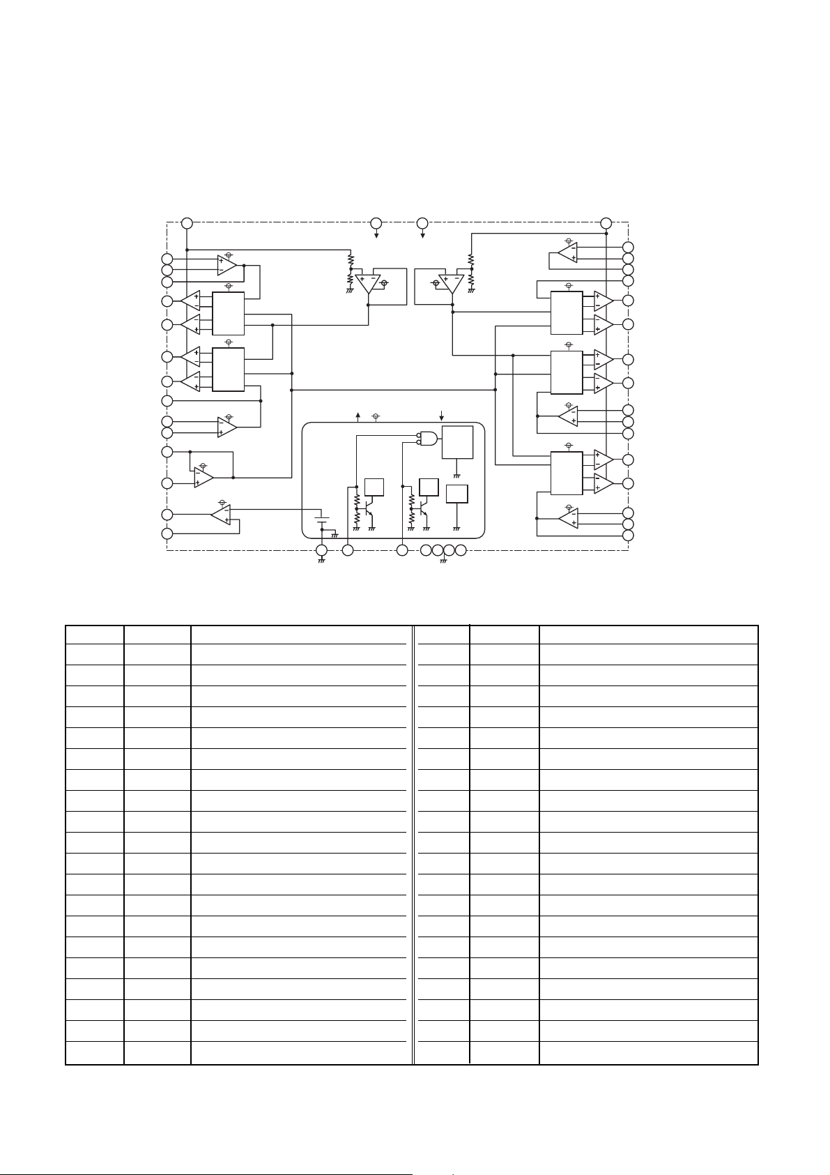
52
IC501 (M56788AFP)
1) It controls the sled movement in track search mode and takes the tray to open/close.
2) It controls the Focus/Tracking Actuator receiving the focus error or tracking error signal from IC101.
Block Diagram
• Pin Description
VBS1
Vm1
VBS1 VBS2
Vm2
IN3-
IN3+
OUT3
CH3IN
VM3(+)
VM3(-)
VM4(+)
VM4(-)
IN4-
IN4+
OUT4
VM5(+)
VM5(-)
IN5+
OUT5
IN5-
IN1+
IN1-
OUT1
VM1(+)
VM1(-)
VM2(+)
VM2(-)
OUT2
IN2-
IN2+
VREFO
VREF
REGB
REG+
SS.GND
MUTE1
MUTE2
GND(4PINS)
VBS2
VBS2
VBS2
VBS2
VBS2
E3
E4
E5
VBS1
CH1
x5
CH3
x8
CH4
x8
VBS2
CH5
x8
VBS1
R
R
R
R
Vrefm1
Vrefm2
VREFO
BIAS
VBS1
Hi:Sleep
Vm1 Vm2
VBS1
E2
VREF
VBS2
1.25v
Low, Open
MUTE ON
SLEEP
5CH
1-4
CH
TSD
VREG
VBS1
CH2
x5
38 5
8
2
1
10
9
12
13
20
19
21
14
15
17
18
19
3
39 4
40
37
36
34
35
32
31
30
28
27
22
23
41
42
24 26 25 7 11 29 33
Terminal
Symbol Terminal function
1 CH3IN CH3 non-inverted input
2 OUT3 E3 amplifier output
3 IN3- E3 amplifier inverted input
4 VBS2 Bootstrap power supply
5 Vm2 Motor power supply
6 N.C. N.C.
7, 11 GND Motor GND
8 IN3+ E3 amplifier non-inverted input
9 VM3(-) CH3 inverted output
10 VM3(+) CH3 non-inverted output
12 VM4(+) CH4 non-inverted output
13 VM4(-) CH4 inverted output
14 VM5(+) CH5 non-inverted output
15 VM5(-) CH5 inverted output
16 OUT5 E5 amplifier output
17 IN5- E5 amplifier inverted input
18 IN5+ E5 amplifier non-inverted input
19 IN4+ E4 amplifier non-inverted input
20 IN4- E4 amplifier inverted input
21 OUT4 E4 amplifier output
Terminal
Symbol Terminal function
22 VREF0 Reference voltage output
23 VREF Reference voltage input
24 SS.GND Small signal GND
25 MUTE2 CH5 mute
26 MUTE1 CH1-4 mute
27 IN2+ E2 amplifier non-inverted input
28 IN2- E2 amplifier inverted input
29,33 GND Motor GND
30 OUT2 E2 amplifier output
31 VM2(-) CH2 inverted output
32 VM2(+) CH2 non-inverted output
34 VM1(+) CH1 non-inverted output
35 VM1(-) CH1 inverted output
36 OUT1 E1 amplifier output
37 IN1- E1 amplifier inverted input
38 Vm1 Motor power supply
39 VBS1 Bootstrap power supply
40 IN1+ E1 amplifier non-inverted input
41 REGB Regulator PNP base connect
42 REG+ Regulator voltage setting resistor
Page 45

53
IC510 (BA6664FM) : Spindle Motor Drive IC
It drives the spindle motor receiving the spindle control signal at IC201 (MICOM) and IC101 (OTI-9795).
2
4
7
8
9
10
28
27
26
25
24
23
22
21
20
19
18
17
16
15
11
12
13
14
TL
TSD
GAIN
CONTROL
Hall 1
Hall 2
Hall 3
Hall Bias
BRAKE MODE
HALL AMP
SHORT BRAKE
P S
A3
A2
A1
H1+
H1-
H2 +
H2 -
H3 +
H3 -
FIN
GND
R
NF
RNF
VM
GSW
VCC
FG
VM
PS
EC
ECR
FR
FG2
SB
CNF
BR
VH
+
-
+
-
+
-
+
+
-
-
+
-
+
-
TORQUE
SENSE AMP
SERVO
SIGNAL
CURRENT
SENSE AMP
VCC
VCC
Vcc
VCC
D
CK
Q
Q
R
DRIVER
GAIN
SWITCH
+
-
Pin No.
1
2
3
4
5
6
7
8
9
10
11
12
13
14
15
16
17
18
19
20
21
22
23
24
25
26
27
28
FIN
Description
N.C.
Output3 for motor
N.C.
Output2 for motor
N.C.
N.C.
Output1 for motor
GND
Positive input for hall input Amp1.
Negative input for hall input Amp1.
Positive input for hall input Amp2.
Negative input for hall input Amp2.
Positive input for hall input Amp3.
Negative input for hall input Amp3.
Hall bias terminal
Brake Mode terminal
Capacitor connection pin for phase compensation
Short brake terminal
3 Phase synthesized FG signal output terminal
Rotation detect signal output terminal
Torque control standard voltage input terminal
Torque control voltage input terminal
START/STOP Switch
FG signal output terminal
Power supply for signal division
Gain Switch
Power supply for driver division
Resistance connection pin for output current sense
GND
Pin Name
N.C.
A
3
N.C.
A
2
N.C.
N.C.
A
1
GND
H
1
+
H
1
-
H
2
+
H
2
-
H
3
+
H
3
-
V
H
BR
C
NF
SB
FG
2
FR
E
CR
E
C
PS
FG
V
CC
GSN
V
M1
R
NF
FIN
Block Diagram
• Pin Description
Page 46

77
Optical
Pick-up
SF-W03PDX
Spindle
Motor
FCS
TRK
SLED
Stepping
Motor
Tray
Motor
Writing
Strategy
Spindle
Drive
Focus
Tracking
Drive
Serial
S/H Timing
RF
IC363
IC404
Servo Signals
Address/Data
Signal
Measuring
Laser
Power
Ref.
IC202
AT93C86
EEPROM
IC501 M56788AFP
Single Chip DRIVE
IC401
OTI-9071AB
RF Amp
Wobble
ALPC
IC201
MB90F476
System
Controller
33.8688MHz
IC101
OTI9795
DSP/Servo
DECODER
ENCODER
ATIP Demodulator
Write Strategy
I/F
Data
IC103
8MB
SDRAM
H
O
S
T
I/F
Cable
IC601
Audio
H/P Amp
L,R
L,R
Line Out
Headphone
Jack
IC510 BA6664FM
MOTOR DRIVE
IC403
BU2500FV(DAC)
Stepping/Tray/Ref.
Control
IC400
IC361
BLOCK DIAGRAM
1. OVERALL BLOCK DIAGRAM
Page 47

78
IC 301
MB90F476
u-COM
IC 201
MB90F476
u-COM
CN102
41 42 43 44
CN102
41 42 43 44
+12
V
GND
GND
+5V
L104
Bead
L100
Bead
IC 106
XC61AN
RESET
IC 106
XC61AN
RESET
IC 180
BA033S
r
IC 180
BA033S
Regulator
3.3V
4V
(2Vref)
IC 401
OTI9071
RF IC
IC 401
OTI9071
RF IC
12V
5V
IC 501 M56788FP
FCS/TRK/SLD/TRY
Driver
IC 501 M56788AFP
FCS/TRK/SLD/TRY
Driver
IC 500
NJM3414
OP Amp
IC 500
NJM3414
OP Amp
2V_ACT
/RESET
Act_Mute
/RFCS
IC 101
OTI-9795
DSP/Servo
/ATAPI
IC 101
OTI-9795
DSP/Servo
/ATAPI
/PRST
/UCS0,1
URDY,URD,UWR
UA[0:8],UAD[0:15]
IC 403
BU2500F
DAC
IC 403
BU2500F
DAC
IC 202
AT93C86
EEPROM
IC 202
AT93C86
EEPROM
/DACS
SDATA, SCLK
SDATA, SCLK
/EPCS
SDATA, SCLK
From HOST
2V
(Vref)
Voltages Used 12V
5V
4V(2Vref)
2V(Vref)
2V(Fvref)
IC 402
NJM3414
OP-Amp
IC 402
NJM3414
OP-Amp
FVref
(2V)
IC 363
D-FF
IC 363
74VHC175
D-FF
2. Power Block Diagram
Page 48

79
IC 401
OTI-9071
IC 362
IC 101
OTI-9795
IC 201
MB90F476
u-COM
MD
IC 510
BA6664
Drive
DMO
IC 500
NJM3414
EC
IC 501
M56788
Drive
FAO/TAO
SLO
TRY+/-
FCS+/-
TRK+/-
U,V,W
HU,HV,HW
IC 403
BU2500, DAC
TRY CTL
A,B,C,D,E,F,G,H
EFM1,2,3
/UCS0,1, URDY,URD,UWR
UA[0:8],UAD[0:15]
FE
TEBC
TE
ATFG
IC 362
74VHC08
RX, XTOR
RX
CE
WBLIN
CE
TE
TZC TX
RECD1,2, XTOR
BS
SPDL FG
BS
IC 404
BU4052
/SDINT, /UINT
STEP_CTRL0
STEP_CTRL1
SM_A+/-
SM_B+/-
MPXOUT1,MPXOUT2
BHO1,PHO1
FE/VRDC1
TE/VWDC
OUTEN2,OUTEN3,OSCEN LDON
IC 361
IC 360
WFPDSH,RFPDSH
ROPC1,RESAMP1
WGATE,EFMNT4
RWGUP
CDR/RW TESTWR
RWPTCTL
WGATE,ESFS
3. Control Signal Block Diagram
Page 49
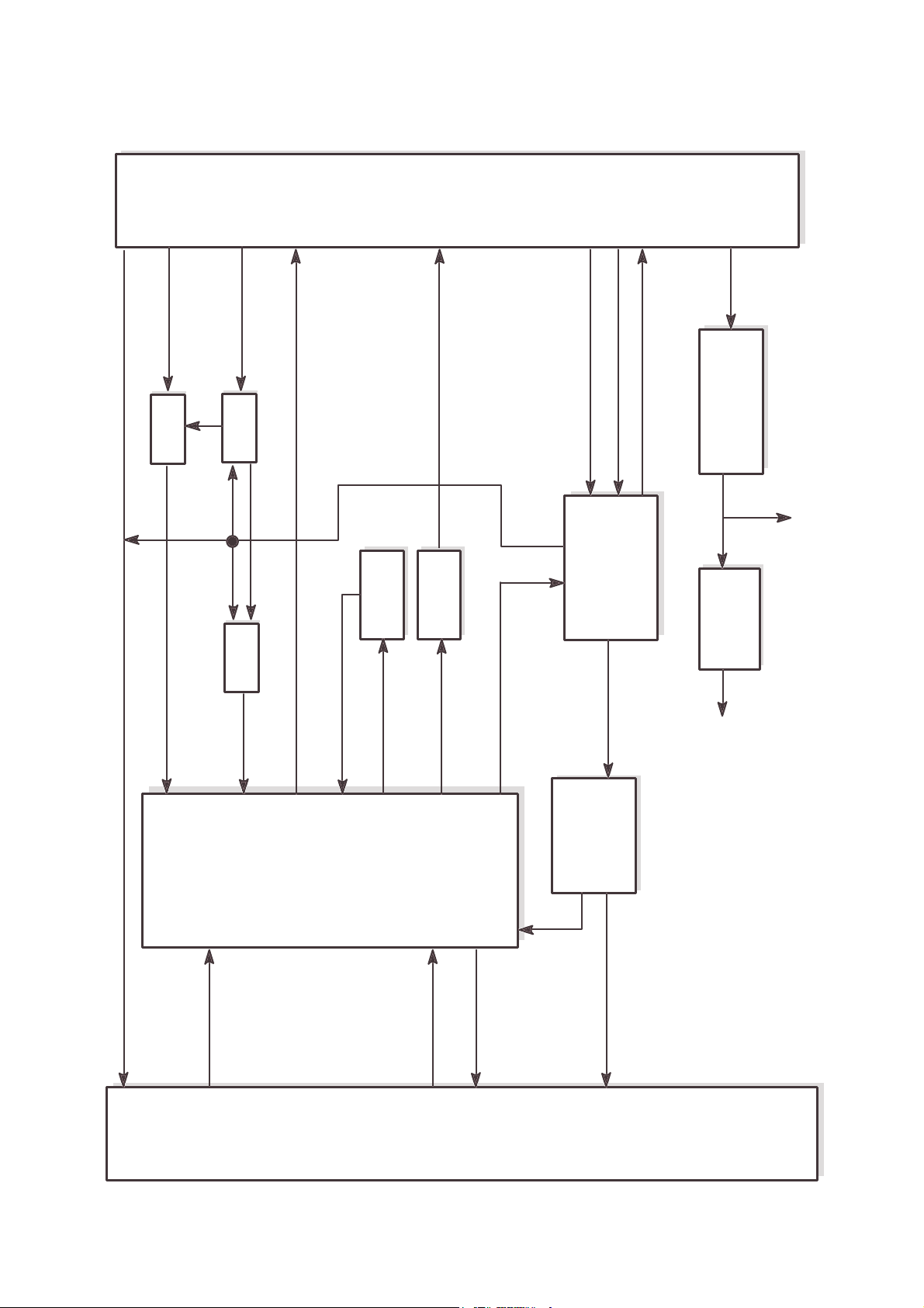
80
A,B,C,D,E,F,G,H
FPDO
VRDC, VWDC1
MD
WREF
RPOWER
VWDC2
IC403
BU2500FV
DAC
/DACS
SDATA,SCLK
ASYM1,2
IC401
OTI-9071
ASP
RRF(RFDC)
RRFIN 1, 2
EQRFN,EQRFP
OUTEN2,OUTEN3,OSCEN
WFPDSH,RFPDSH
LDON
RWGUP
CDR/RW TESTWR
RWRPCTL
R-C
Circuit
IC 360
IC 362
IC 361
IC400
KM4200
IC201
MB90F476
-COM
/UCS0,1,URDY,URD,UWR
UA[0:8],UAD[0:15]
Lout
Line out
Rout
Q603
Mute Control
IC601
H/P Amp
H/P Out
EFM(RFAC)
BS
BS
IC101
OTI-9795
EFM1,2,3
ROPC1, RESAMP1
WGATE,ESFS
/SDINT, /UINT
WGATE,EFMNT4
4. Read/Write Signal Block Diagram
Page 50

032
PBM00 (MAIN C.B.A)
007
A02
A01
020
028
028
400
400
400
400
021
020
030
050
413
413
413
001
413
430
011
009
008
012
014
005
034
016
015
004
006
031
A B C D E F GH
1
2
3
4
5
017
003
002
010
400
400
029
420
027
033
025
026
419
11 1 2
EXPLODED VIEW
 Loading...