

Page 1

3
INTRODUCTION
FEATURES
1. General
1) Enhanced IDE interface.
2) Internal 5.25 inch, halfheight CD-R/RW Drive.
3) 2 Mbytes buffer memory.
4) Audio CD like tray loading of a disc without using a caddy.
5) Power loading and power ejecting of a disc. The disc can also be ejected manually.
6) Supports Power saving mode and Sleep mode.
7) Vertical and Horizontal operation.
2. Supported disc formats
1) Reads and writes data in each CD-ROM, CD-ROMXA, CD-I FMV, Video CD, and CD-EXTRA
2) Reads data in Photo CD (Single and Multi session).
3) Reads and writes standard CD-DA.
4) Reads and writes CD-R discs conforming to “Orange Book Part 2”.
5) Reads and writes CD-RW discs conforming to “Orange Book Parts 3”.
3. Supported write method
1) Disc at once (DAO), Session at once (SAO), Track at once (TAO), Variable packet, Fixed packet, and
Multi-session.
4. Performance
1) Random 100 ms average access time.
2) Max 4,800 kB/sec (Max 32X) Sustained Transfer rate.
3) Supports real time error correction and real time layered error correction at each speed.
4) Supports CD-R write operation at double speed, quadruple speed, and eight speed.
5) Supports CD-RW write operation at double speed and quadruple speed.
6) PIO Mode 4 & Multi DMA Mode 2 Support.
7) MPC-3 Spec compliant.
5. Audio
1) Output 16 bit digital data over ATA interface.
2) 4 Times Digital Filter for CD Audio
3) Software Volume Control
4) Equipped with audio line output and headphone jack for audio CD playback.
5) Front panel Volume Control for Headphone Output.
This service manual provides a variety of service
information.
It contains the mechanical structure of the CDR/RW Drive and the electronic circuits in
schematic form. This CD-R/RW Drive was
manufactured and assembled under our strict
quality control standards and meets or exceeds
industry specifications and standards.
This CD-R/RW drive is an internal drive unit
designed for use with IBM PC, HP Vectra, or
compatible computer. It can write as much as 650
Mbytes of digital data into CD-R/RW disc, and can
read as much as 650 Mbytes of digital data stored
in a CD-ROM, CD-R and CD-RW disc.
This CD-R/RW Drive can easily meet the
upcoming MPC level 3 specification, and its
Enhanced Intelligent Device Electronics (E-IDE)
and ATAPI interface allows Plug and play
integration in the majority of today’s PCs without
the need of an additional interface card.
Page 2

4
SPECIFICATIONS
1. SYSTEM REQUIREMENTS
-CPU: IBM Compatible Pentium 233MHZ (or faster)
(For 8X Write speed, 266MHz or faster recommended.)
-32MB Memory or greater
2. SUPPORTING OPERATING SYSTEM
3. GENERAL
1) Host Interface.......................................................................................................................ATAPI compliant
2) Read Function
• Acceptable discs ...............................................................CD-ROM Mode1 (basic format), CD-ROM XA
CD-Audio
Mixed Mode (Audio and Data Combined)
Photo-CD (Single and Multi-Session)
CD-I Ready, Video CD
CD-Plus/CD-Extra,
CD-R (Conforming to “Orange Book Part2”)
CD-RW (Conforming to “Orange Book Part3”)
3) Write function
• Applied Format..................................................................CD-ROM Mode-1
CD-ROM XA
CD-Audio
Mixed Mode (Audio and Data Combined)
Video CD
CD-Plus/CD-Extra,
• Writing Method..................................................................Disc at once(DAO)
Session at once(SAO)
Track at once(TAO)
Variable packet writing
Fixed packet writing
Multi-session
4) Cache memory (R/W) .........................................................2 Mbyte
5) Disc diameter ......................................................................12 cm (8 cm Read only)
6) Data capacity (Yellow-Book)
• User Data/Block ................................................................2,048 bytes/block (Mode 1 & Mode 2 Form 1)
2,336 bytes/block (Mode 2)
2,324 bytes/block (Mode 2 Form 2)
2,352 bytes/block (CD-DA)
7) Rotational Speed
CD-Audio.............................................................................6x~15x(CAV) Approx.3000 rpm
CD-RW data ........................................................................8x~20x(CAV) Approx.4000 rpm
CD-ROM/CD-R data............................................................14x~32x(CAV) Approx. 7000 rpm
8) MTBF
• 120, 000 POH at an operating duty of 10% at room temperature.
4. DRIVE PERFORMANCE
1) Data Transfer Rate
* Sustained Data Transfer Rate ..........................................150 Kbytes/s (1x)
300 Kbytes/s (2x)
600 Kbytes/s (4x)
1,200 Kbytes/s (8x)
2,400 Kbytes/s (16x)
2,100 to 4,800 Kbytes/s 14 to 32x CAV
• DOS 3.1 or Higher
• Windows ‘95/’98
• OS/2 Warp (Ver 3.0)
• Solaris Ver 2.4 or higher
• Linux Slackware Ver 2.3
• Windows NT 4.0 or later
Page 3
5
* Burst Data Transfer Rate (ATAPI) ....................................16.67 Mbytes/sec (PIO Mode 4)
16.67 Mbytes/sec (MULTI-DMA Mode 2)
2) Average Access Time
Random Access ..................................................................100 ms Typical (Max.32X) : INCLUDING LATENCY
3) Data Buffer Capacity ...........................................................2 Mbytes
5. POWER REQUIREMENTS
1) Voltage
+5 V DC with + 5% tolerance, less than 100 mVp-p Ripple voltage
+12 V DC with +5% tolerance, less than 100 mVp-p Ripple voltage
2) Current
• Hold Track State ...............................................................+5V DC 1.0A, +12 V DC 0.8A
• Seeking & Spin up ............................................................+5 V DC 1.2A, +12 V DC 1.0A
6. AUDIO PERFORMANCE
* CED-8080B/CED-8083B DIFFERENCES TABLE
Item Typical Limit Test Signal Test Condition Note
Output Level
0.7 Vrms
+
10 % 1KHz 0 dB No Filter at 47 kΩ
S/N 75 dB 70 dB 1KHz 0 dB with IHF-A + 20KHz LPF at 47kΩ
THD 0.2 % 0.25 % 1KHz 0 dB with IHF-A + 20KHz LPF at 47kΩ
Channel
70 dB 65 dB 1KHz 0 dB with IHF-A + 20KHz LPF at 47kΩ
Separation
Frequency +
2dB
Response
H/P
Output Level
AUDIO OUT
+
3 dB 20Hz~18KHz 0 dB No Filter at 47 kΩ
0.6Vrms
+
20 % 1KHz 0dB No Filter H/P Volume MAX at 32 Ω
Funtion CED-8080B CED-8083B
• CD-R Writing speed 2x/4x/8x Data writing 2x/4x Data writing
• CD-RW Writing speed 2x/4x Data writing 2x/4x Data writing
• CD-ROM Reading speed 32x Data transfer 32x Data transfer
MODEL
Page 4
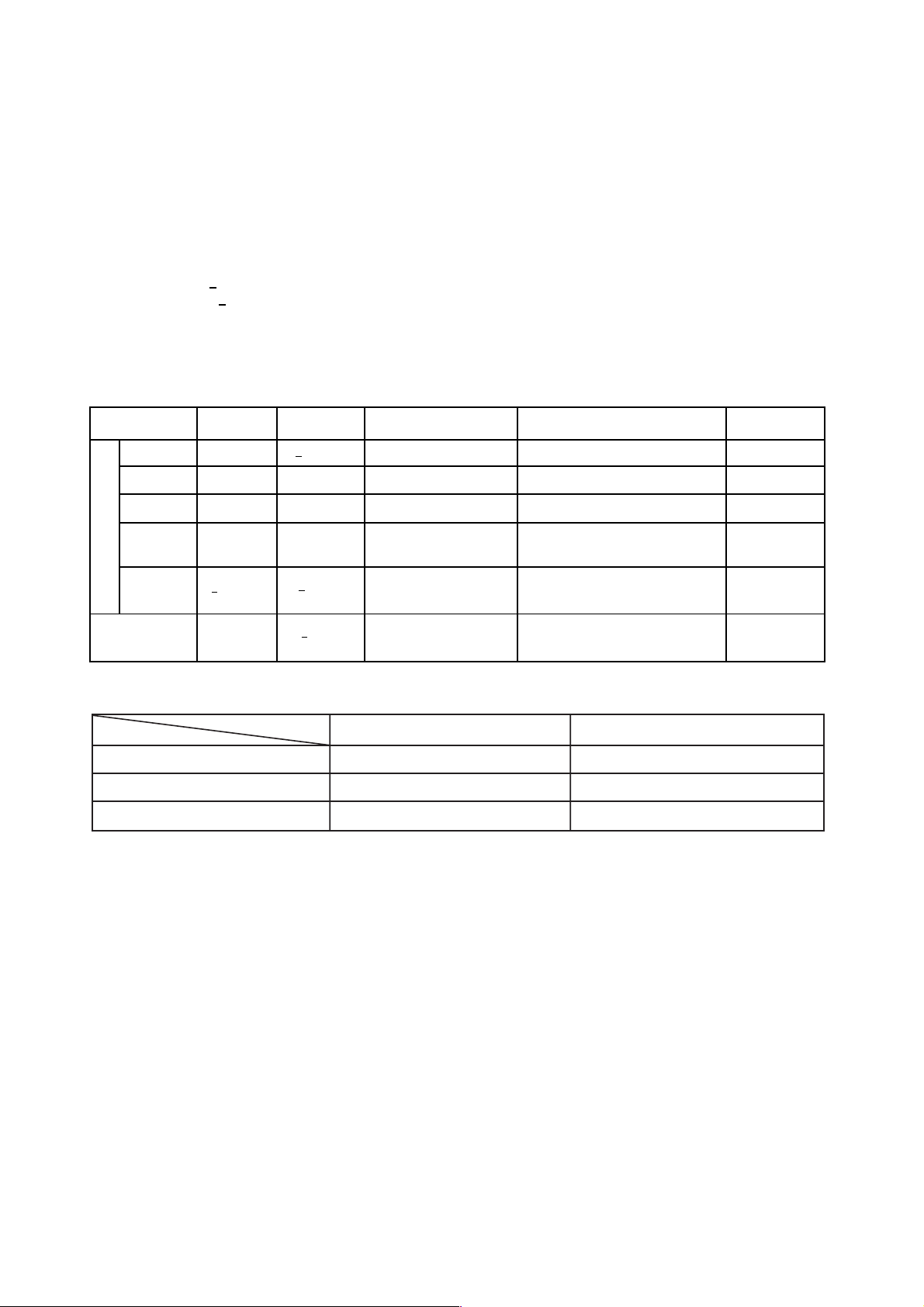
LOCATION OF CUSTOMER CONTROLS
6
1. Disc tray
This is the tray for the disc. Place the disc on the
ejected disc tray, then lightly push the tray (or
push the eject button) and the CD will be loaded.
NOTE: Don’t pull out or push in the disc tray
forcibly. This might cause damage to the loading
section of the drive.
2. Stop/Eject button
This button is pressed to open the CD tray.
This button works only when power is supplied to
the drive.
If an Audio CD is playing, pressing this button will
stop it, and pressing it again will open the tray.
3. Play/Skip button
When an Audio CD is in the disc drawer, pressing
this button will start playing Audio CDs from the
first track. If an Audio CD is playing, pressing this
button will skip to the next track.
4. Volume control
This is used to adjust the output volume of the
headphone jack. It can’t be used to adjust the
output volume for the audio output connectors on
the rear panel.
NOTE : Turn the volume down before turning on
the power. Sudden loud noises can damage your
hearing.
5. Headphone jack
This jack is for connecting headphones or minispeakers.
6. Drive activity indicators
Two colored LEDs are used to indicate the
operation of CD-R/RW Drive.
(1) Read
The orange color is displayed when the spindle
motor begins the Spin up operation: accessing
data, reading data, playing Audio, and up loading
tray.
(2) Write
The green color is flashed during disc writing
sessions.
READ
READ
WRITE
WRITE
COMPACT
Headphone Jack
Volume
Control
Drive Activity Indicators
Play/Skip Button
Stop/Eject Button
Disc Tray
Front Panel
Page 5
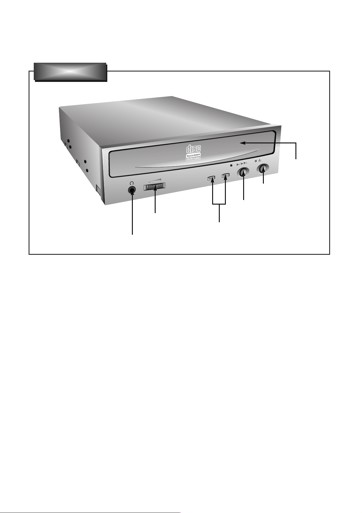
7
1. Power Connector
Connects to the power supply (5-and 12-V DC) of
the host computer.
NOTE : Be careful to connect with the proper
polarity. Connecting the wrong way may damage
the system (and is not guaranteed). Usually this
connector can only be attached one-way.
2. IDE Interface Connector
Connect to the IDE (Integrated Device
Electronics) Interface using a 40-pin flat IDE
cable.
NOTE : Do not connect or disconnect the cable
when the power is on, as this could cause a short
circuit and damage the system. Always turn the
power OFF when connecting or disconnecting the
cable.
3. Jumper Connector
This jumper determines whether the drive is
configured as a master or slave. Changing the
master-slave configuration takes effect after
power-on reset.
4. Analog Audio Output Connector
Provides output to a sound card (analog signal).
Generally you need this to play a regular audio
CD.
5. Digital Audio Output Connector
Provides output to a sound card (digital signal).
DIGITAL ANALOG
INTERFACE POWER
D
R
CS M
S
LA
G
LG39
1
+5
+12
GND
40
2
AUDIO AUDIO
Digital Audio Output
Connector
Jumper Connector
Analog Audio Output Connector
IDE Interface Connector
Power Connector
Rear Panel
Page 6
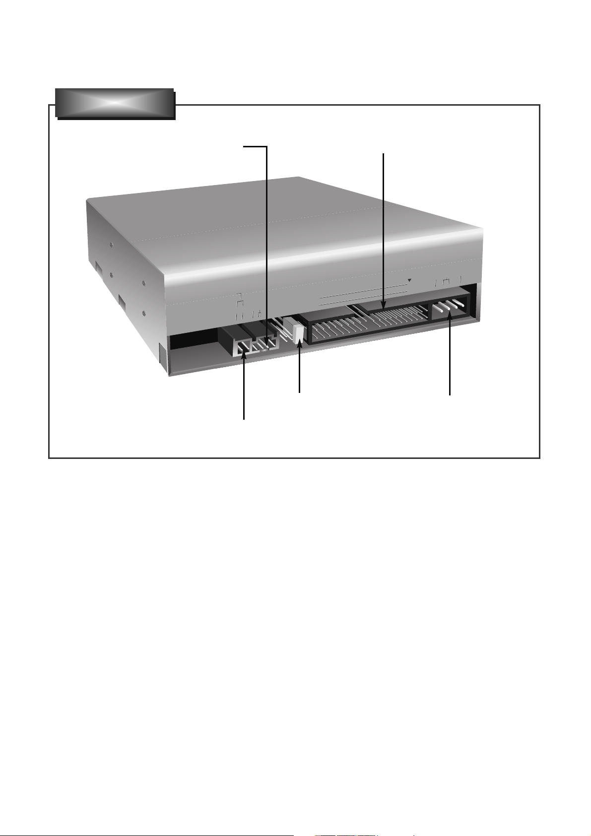
1. CABINET and CIRCUIT BOARD
DISASSEMBLY
1-1. Bottom Chassis
A. Release 4 screws (A) and remove the Bottom Chassis
in the direction of arrow (1). (See Fig.1-1)
1-2. Front Bezel Assy
A. Insert and press a rod in the Emergency Eject
Hole and then the CD Tray will open in the direction
of arrow (2).
B. Remove the Tray Door in the direction of arrow
(3) by pushing the stoppers forward.
C. Release 3 stoppers and remove the Front Bezel Assy.
1-3. Cabinet and Main Circuit Board
A. Remove the Cabinet in the direction of arrow (4).
(See Fig. 1-3)
B. Release 2 hooks (a) and remove the CD Tray
drawing forward.
C. Remove the Main Circuit Board in the direction of
arrow (5).
D. At this time, be careful not to damage the 4
connectors, are positioned at left side, of the Main
Circuit Board.
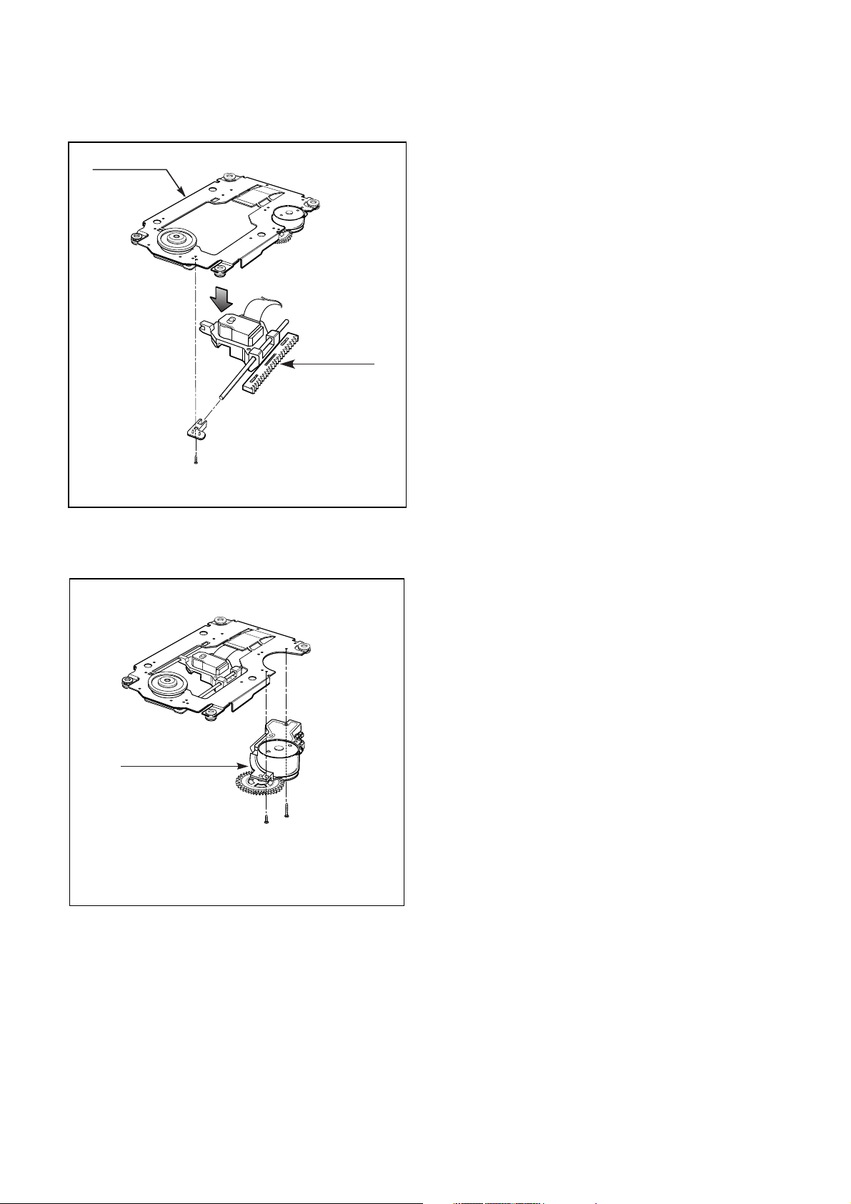
2. MECHANISM ASSY DISASSEMBLY
2-1. Pick-up Unit
A. Release 2 screws (B).
B. Separate the Pick-up Unit in the direction of arrow (6).
(4)
(5)
Main
Circuit Board
Cabinet
Hooks (a)
Fig. 1-1
Fig. 1-2
DISASSEMBLY
8
Fig. 1-3
Mechanism Assy
Pick-up Unit
(B)
(B)
(6)
Fig. 1-4
(1)
(A)
Bottom Chassis
(A)
(A)
(A)
Tray Door
(3)
Stoppers
Emergency Eject Hole
(2)
Front Bezel Assy
CD Tray
Page 7
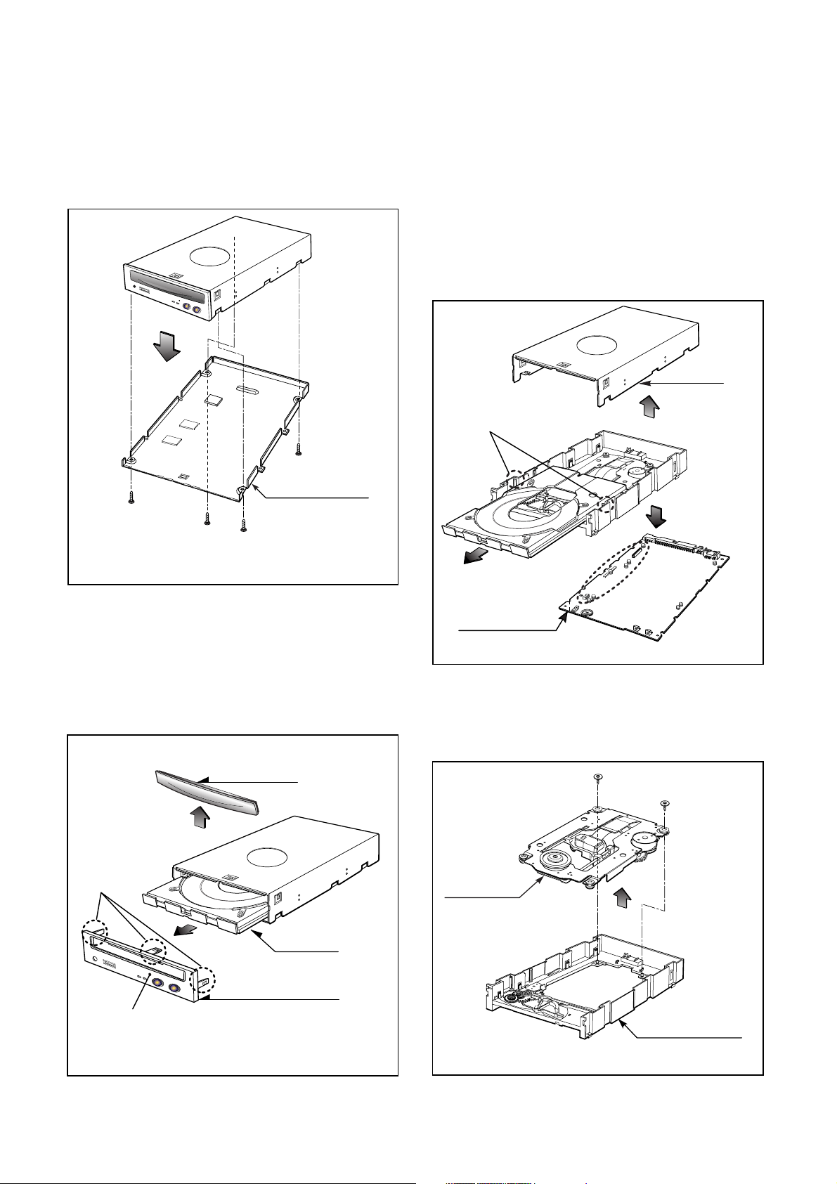
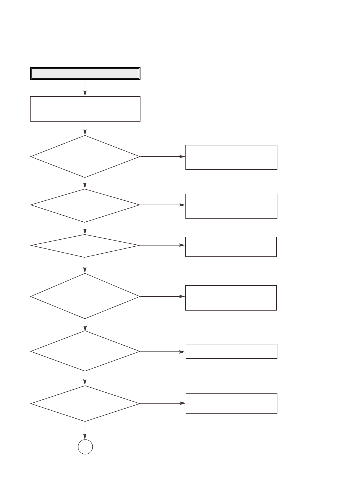
2-2. Pick-up
A. Release 1 screw (C) and remove the Pick-up.
2-3. Sled Motor Assy
A. Release 2 screws (D),(E) and remove the Sled
Motor Assy.
(D)
(E)
Sled Motor Assy
Fig. 1-5
9
Fig. 1-6
Pick-up Unit
(C)
Pick-up
Page 8
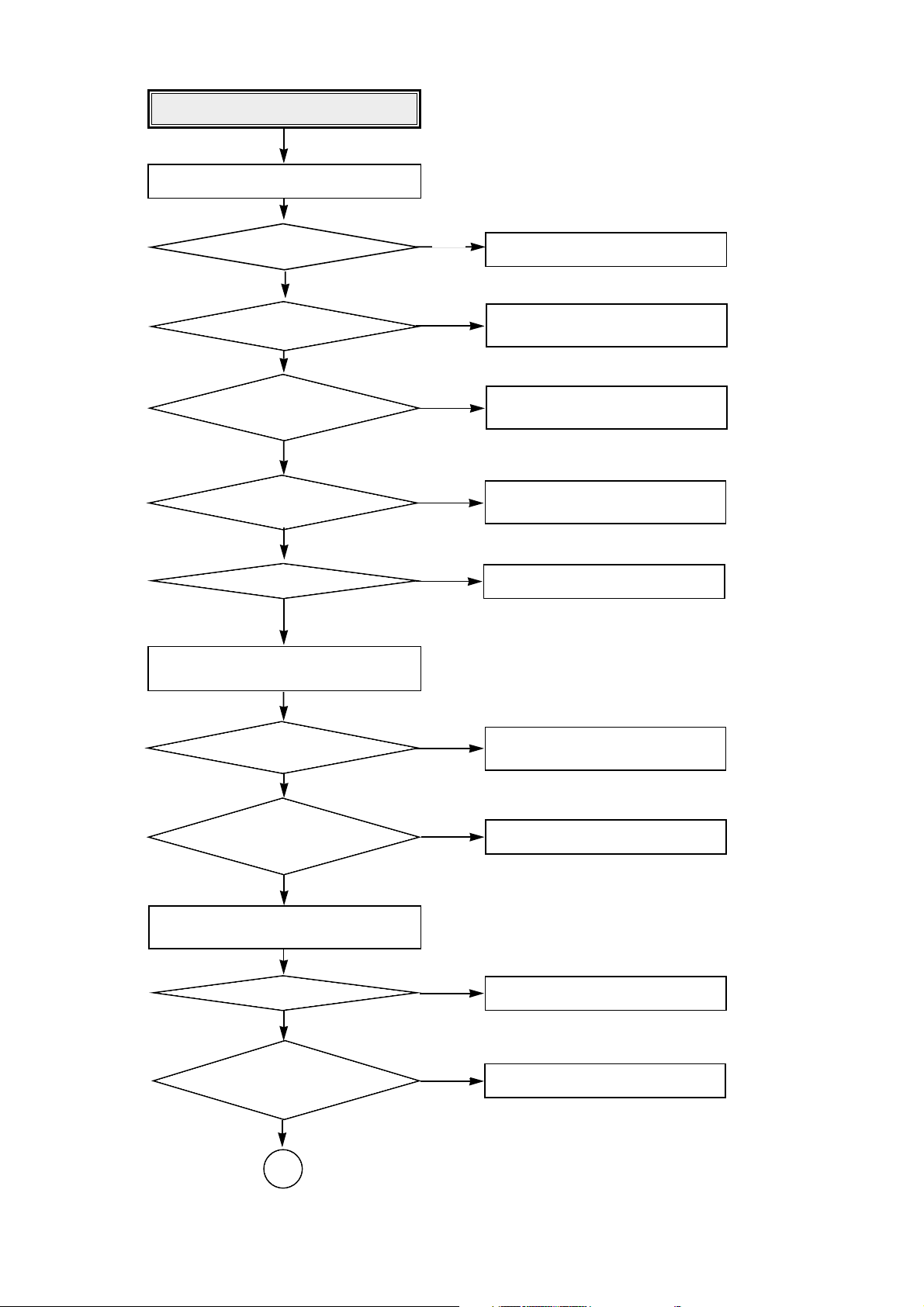
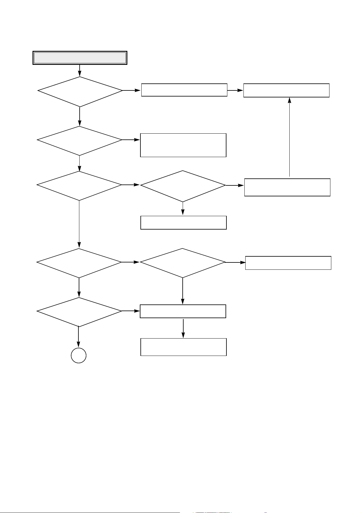
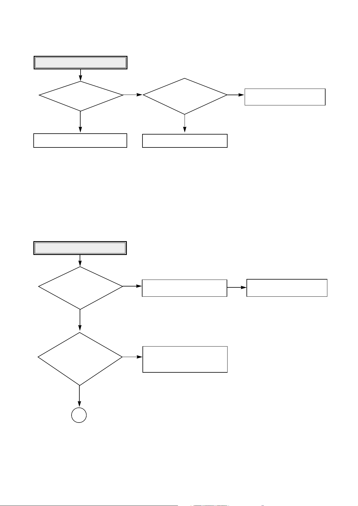
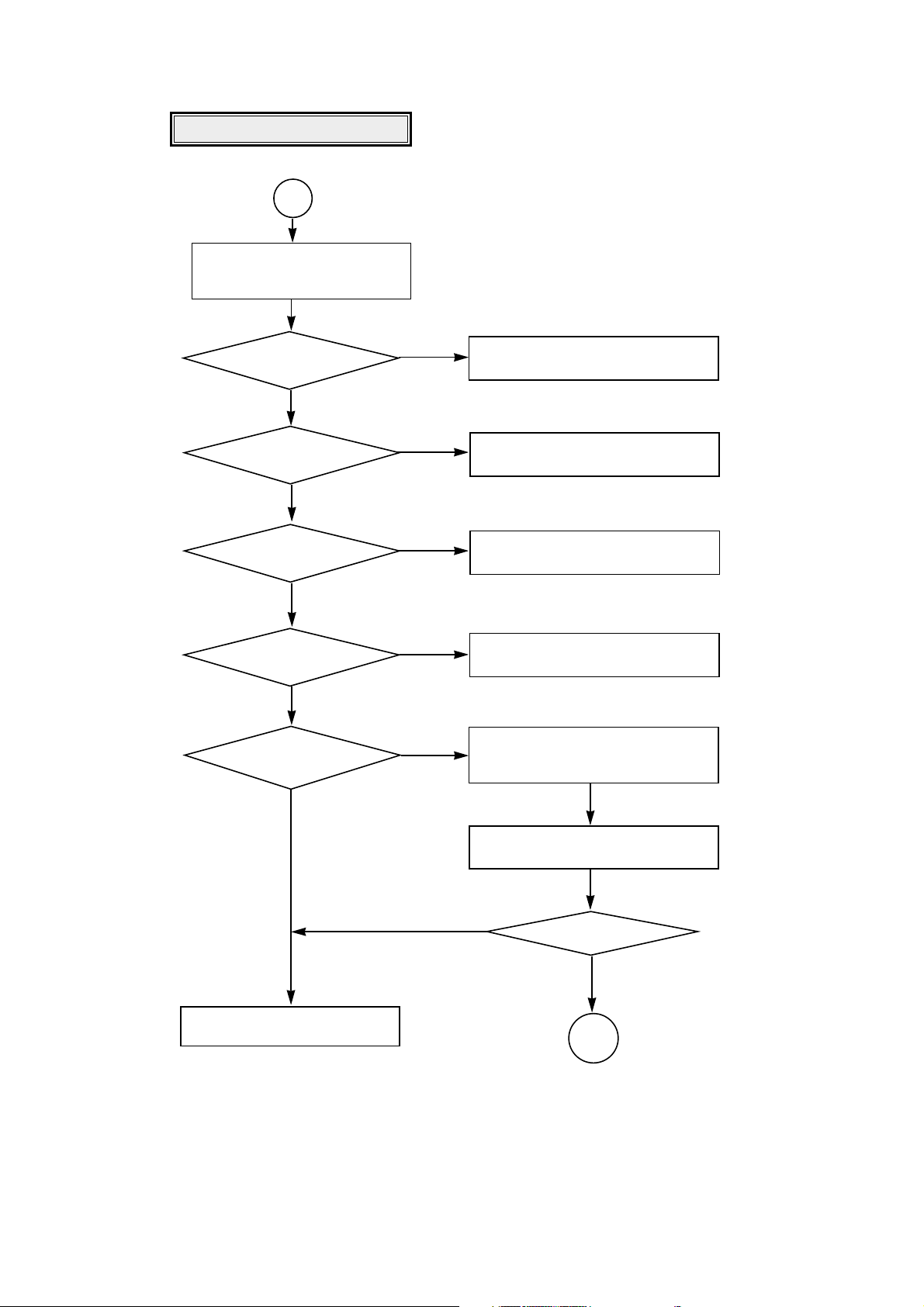
TROUBLESHOOTING GUIDE
Are the pin 41
and 44 of PN201 +12V and +5V
respectively after the power
cable connecting?
Reset or Power Check.
• Check the power(12V, 5V) short.
• Check PC power cable.
• Repair the PC power supply.
• Check the IC101(RESET IC).
• Check the IC102(BA033S), IC201
(OTI-9790), IC301(HD64F3062)
Does the pin 1
of IC101 change 0V to 5V at the
power supply initial input mode?
• Is the pin 4 of IC103 3.9V?
• Is the pin 32 of IC401 2.0V?
• Is the pin 4 of IC102 3.3V?
• Is the pin 7 of IC514 2.5V?
• Is the pin 1 and 2 of IC514 2.0V?
• Is the pin 1 of IC511 8.0V?
• Is the pin 1 of IC512 8.0V?
NO
NO
YES
YES
YES
YES
YES
49
Are the X201 and X301 oscillating?
• Check the X201, X301.
• Check the IC201, IC301.
NO
• Check the IC103(BA3939).
• Check the IC401(CXA2551R).
• Check the IC102(BA033S).
NO
Check the IC514(NJM3414).
• Check the IC511(NJM7808).
• Check the IC512(NJM7808).
NO
NO
Check it after connecting the power cable
only on interface cable for NO Reset or
Power ON.
YES
OK
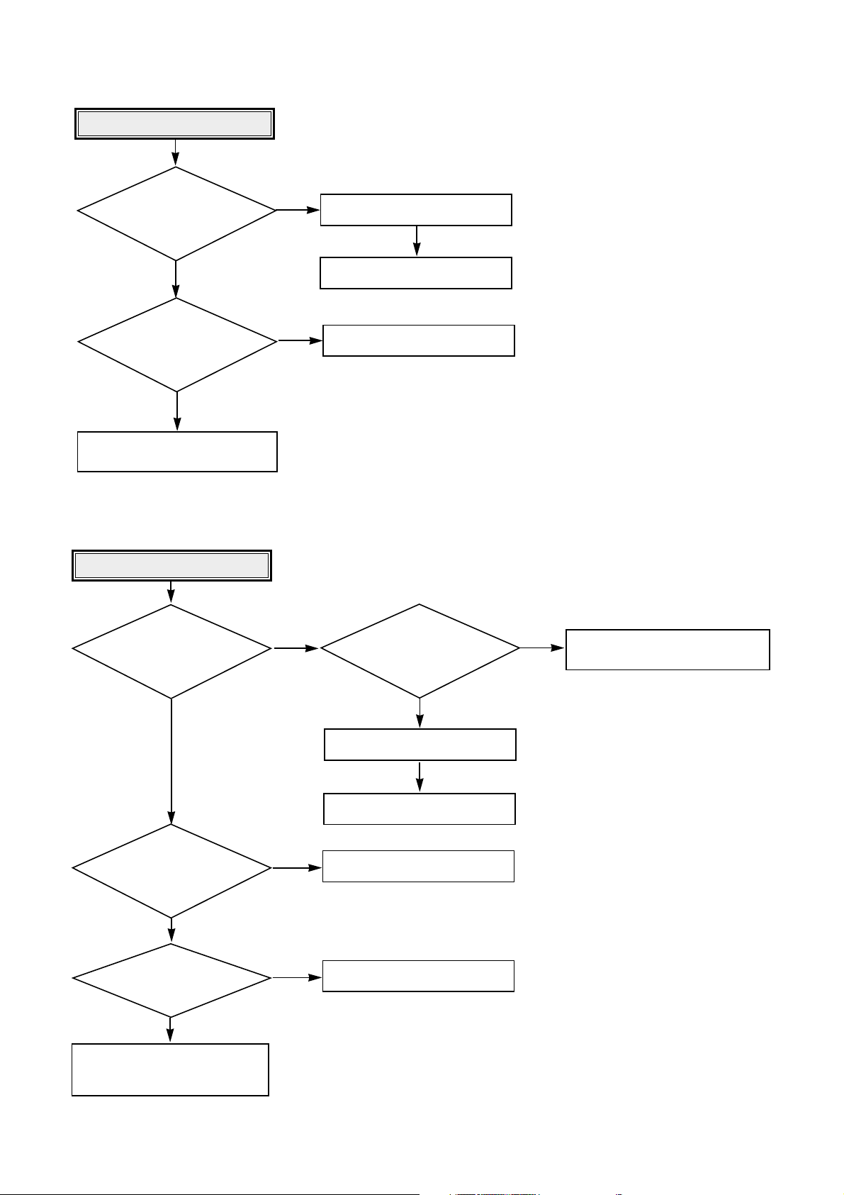
Page 9
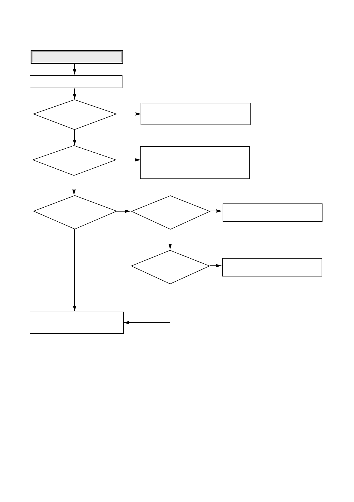
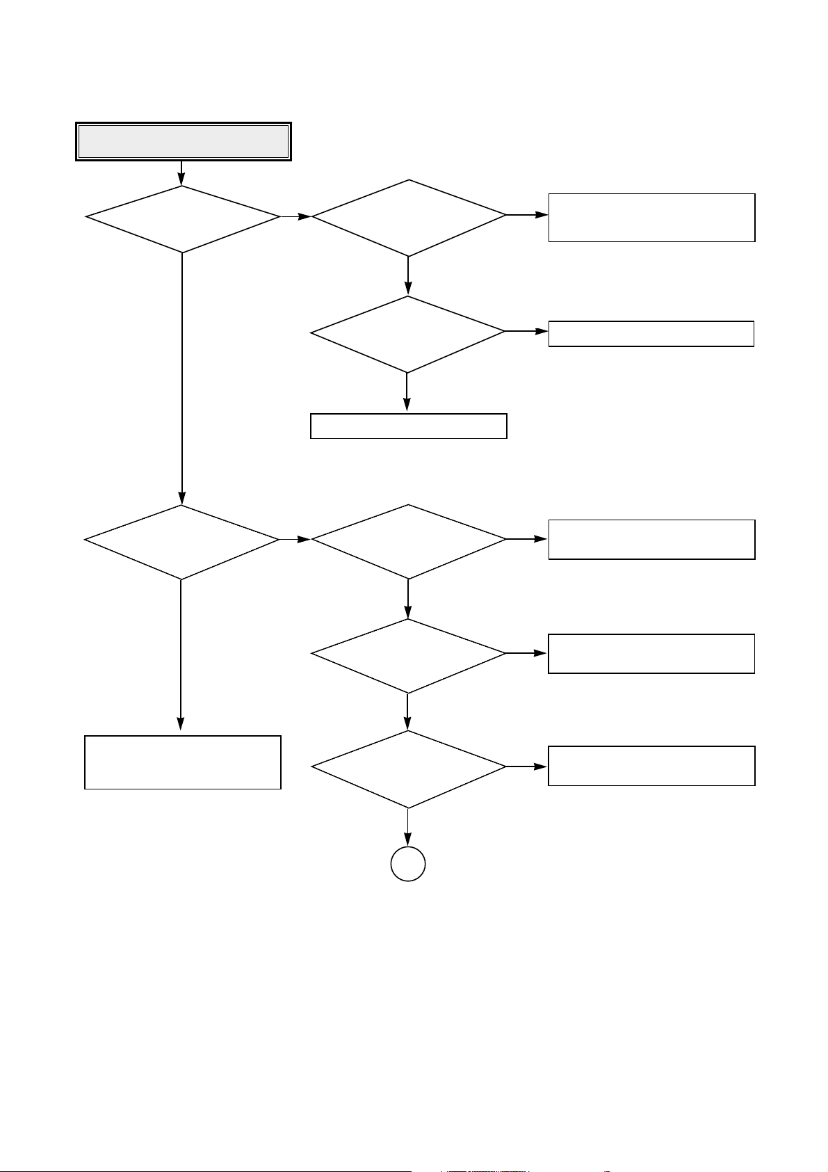
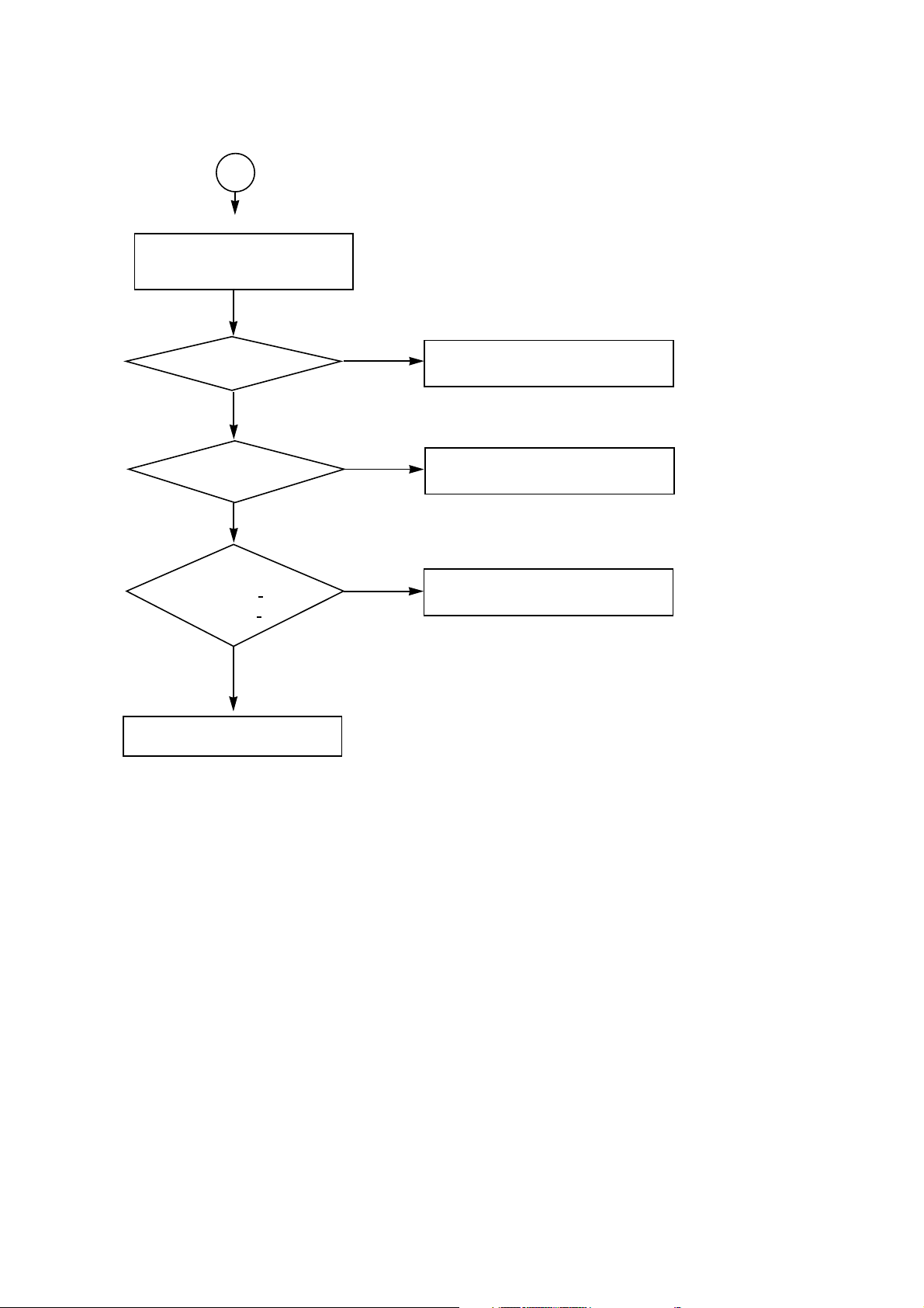
50
System Check.
Go to “Tray operating is abnormal”
Load tray without inserting disc.
NO
Does Tray operate normally?
Does Pick-up move to inside?
Does Spindle Motor
rotate in a moment?
Does Laser turn on?
After eject tray, Inset CD-ROM Disc
and reloading.
Does Disc stop?
Does Disc rotate
continuously as Disc recognition is
abnormal?
After eject tray, Inset CD-R Blank Disc
and reloading.
Does Disc rotate
continuously as Disc recognition is
abnormal?
Does Disc stop?
Go to “Sled operating is abnormal”
Go to “Spindle operating is
abnormal”
Go to “Laser is abnormal”
Go to “Spindle control is abnormal 1”
Go to “Spindle control is abnormal 2”
Go to “Spindle control is abnormal3”
Go to “Disc recognition is abnormal”
NO
NO
NO
YES
NO
NO
NO
NO
YES
YES
YES
YES
YES
YES
YES
Does Lens move
Up/Down?
Go to “Focus Actuator operating is
abnormal”
NO
YES
OK
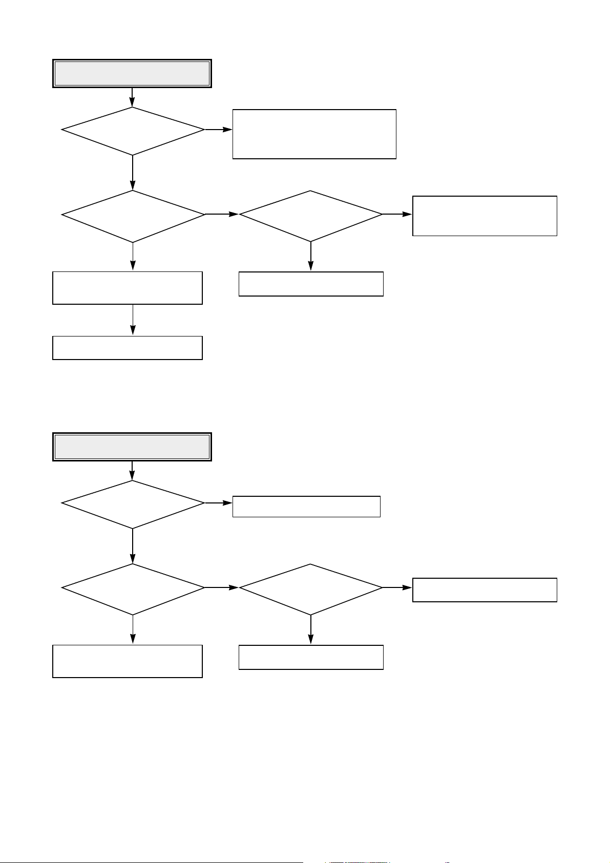
Page 10
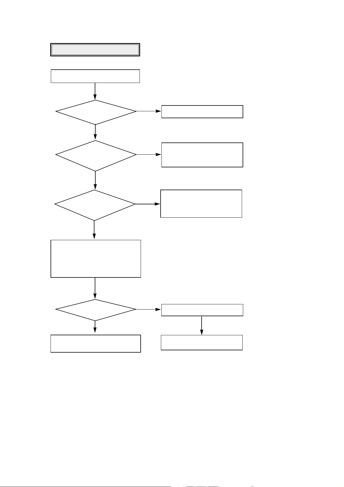
51
Is the input voltage
0V at IC301 pin 52 when push the
SW802?
Tray operating is abnormal.
Is there Tray
drive voltage output?
(IC501 pin 15, 16)
Is TRAY_MUTE signal “L”?
(IC501 pin 20)
• Check the connection of IC201 pin 52.
• Replace the SW802(Eject s/w)
(Tray open/close doesn’t work)
NO
• Check the connection of IC301 pin 25.
• Replace the IC301.
NO
NO
• Check the Tray Connector(PN301).
• Check the Motor Line and Motor.
YES
Is there Tray control signal input?
(IC501 pin 26)
• Check the connection of IC409 pin 12.
• Replace the IC409(M62352).
• Check the communication line between
IC409 and IC301(MICOM).
NO
YES
YES
YES
When PN301
is open, Is there Tray drive
signal output?
• Replace the IC501(BA5983FM).
NO
YES
Page 11
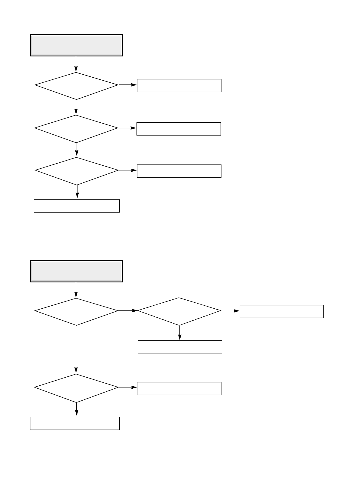
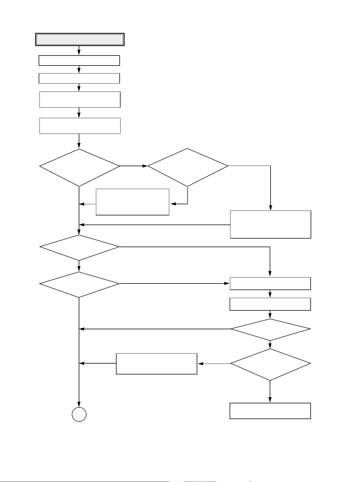
52
Is there Sled
control signal output?
(IC301 pin 85)
Sled operating is abnormal.
Replace the IC501 (BA5983).
Replace the IC508 (BU4053).
NO
Replace the IC301 (MICOM).
NO
Is Act_Mute signal ‘L’?
(IC501 pin 9)
• Check the connction of IC502 pin 17.
• Replace the IC502(BA5925)
Check the connection of IC301
pin 26.
Is there
HALL/SLDOUT signal
input? (IC301 pin 82)
Is there
SLED FG signal input?
(IC301 pin 97)
Check the IC502(BA5925).
NO
Check the connection of IC301 pin 85
NO
NO
YES
YES
YES
YES
Is there
HALL 1 signal input?
(IC508 pin 3)
NO
•
Check the Connector(PN501).
•
Replace the SLED Motor.
NO
Is there Sled drive voltage
input? (IC501 pin 23)
YES
NO
Is there
Sled drive voltage output?
(IC501 pin 17, 18)
YES
YES
OK
Page 12
53
Is there
Spindle control signal input?
(IC510 pin 22)
Spindle operating is abnormal
•
Check the connection of IC201 pin 2.
•
Replace the IC201(OTI-9790).
Is there
DMO signal input?
(IC509 pin 5)
Replace the IC508(BU4053).
Is there
Spindle drive voltage output?
(IC510 pin 2, 4, 7)
•
Check the Spindle
Connector(PN502)
•
Replace the Spindle Motor.
NO
NO
YES
Is SPNON signal “H”?
(IC510 pin 23)
NO
YES
YES
YES
NO
•
Replace the IC509(NJM3404).
• Check the connection of IC301 pin 99.
• Replace the IC301(MICOM).
Is SBRK signal “L”?
(IC510 pin 18)
NO
YES
• Check the connection of IC301 pin 94.
• Replace the IC301(MICOM).
Is there a
SPNFG signal input?
(IC301 pin 7, IC201 pin 95)
NO
YES
• Check the connection of IC510 pin 19.
• Replace the IC510(BA6664FM).
Is there Spindle
control signal output?
(IC509 pin 7)
YES
NO
OK
Page 13
54
Focus Actuator operating is
abnormal
Is there Focus
Search control signal input?
(IC501 pin 3)
Is Act_Mute signal “L”?
(IC501 pin 9)
• Replace the IC501(BA5983).
• Check the connection of PN401 pin 1, 4.
• Check the Pick-up Connector(PN401).
• Check the connection of IC301 pin
26.
• Replace the IC301(MICOM).
NO
YES
• Replace the Pick-Up.
Is there Focus
Search drive voltage output?
(IC501 pin 13,14)
NO
• Check the connection of IC201 pin 207.
• Check the communication line between
IC201 and IC301.
• Replace the IC201 (OTI-9790)
YES
NO
YES
Spindle control is abnormal 1
(CD-ROM Disc)
Does FOCUS Servo
operate normally?
Is there a output normally?
(IC401 pin 71, 72)
• Replace the IC413(EL2245).
Go to “Spindle operating is
abnormal”
• Replace the IC401(CXA2551R).
NO
YES
Is there RFAC signal input?
(IC201 pin 163)
NO
• Go to “Focus Servo is unstable”
YES
NO
YES
Page 14
55
Is there RRF signal input?
(IC413 pin 3)
Spindle control is abnormal 2
(CD-ROM Disc)
Go to “RF output is abnormal”
Is there RFDC signal input?
(IC401 pin 85)
YES
YES
NO
Replace the IC413(EL2245).
NO
Does Tracking Servo
operate normally?
YES
Go to “Track Servo is unstable”
Go to “Disc recognition is abnormal”
NO
Is there WBLIN signal input?
(IC201 pin 132)
Spindle control is abnormal 3
Go to “RF output is abnormal”
Is there ATFM signal output?
(IC401 pin 25)
YES
YES
NO
Replace the IC401(CXA2551R).
NO
Is there DMO signal output?
(IC202 pin 2)
YES
Replace the IC201(OTI-9790).
Go to “Spindle operating is abnormal”
NO
Page 15
56
Is there CDR/RW signal input
normally? (IC601 pin 33)
Go to “Track Servo is unstable”
Disc recognition is abnormal
Replace IC301 (MICOM)
Is there RECD1,
RECD2 signal output normally?
(IC401 pin 48, 49)
Go to “RF output is abnormal”
YES
YES
NO
NO
Is there
PICK UP (A, B, C, D)
output normally?
(PN401 pin 8, 9, 14, 15)
RF output is abnormal
•
Check the PICK UP FFC.
•
Replace the PICK UP.
Go to “Laser is abnormal”
YES
Is RRF
signal output normal?
(IC401 pin 86)
•
First Recognition try: Over 1.7 Vpp
•
Second Recognition try:
Over 0.5 Vpp
YES
NO
•
Check the connection between
PN401 and IC401.
•
Replace the IC401(CXA2551R).
No
OK
Page 16
57
Focus Servo is unstable
Is FE signal
output normal in Focusing
Up/Down?
(IC401 pin 56)
YES
Check the IC401(CXA2551R).
Go to “RF output is abnormal”
Go to “Focus Actuator
operating is abnormal”
NO
Track Servo is unstable
Is TE signal
output normal in Focusing
ON and Tracking OFF?
(IC401 pin 57)
YES
•
Check the PICK UP FFC.
•
Replace the PICK UP.
Check the IC401(CXA2551R).
Go to “RF output is abnormal”
Check the IC403 (NJM3403)
NO
Is TE signal
input normal in Focusing
ON and Tracking OFF?
(IC201 pin 198)
NO
Replace the IC201(OTI-9790).
Check the Driver IC(IC501) and
P/U referring to “Focus Actuator
operating is abnormal”.
Is there TAO
signal output in Tracking ON?
(IC201 pin 208)
NO
Is PICK UP
(E, F, G, H) output normal?
(PN401 pin 16, 7, 13, 10)
YES
YES
YES
YES
NO
Is FAQ signal
output normal in Focusing
Up/Down?
(IC201 pin 207)
Replace the IC201(OTI-9790)
NO
YES
Page 17
58
Is EEPROM Data valid?
Execute ‘B.Calibration Data’ of
‘How to use Test Tool (Dragon)’
Execute ‘D.LD Inspection’ of ‘How
to use Test Tool(Dragon)’
YES
NO
OK?
NO
Laser is abnormal
OFF LEVEL NG?
VRDC NG?
G
E
Normal
F
NO
Execute ‘C.LD Power Setup’ of
‘How to use Test Tool(Dragon)’
NO
YES
NO
VWDC1 NG?
YES
YES
YES
Page 18
59
LD CHECK (Not Read)
Execute ‘E. LD On’ of ‘How to
use Test Tool (Dragon) : ‘VRDC
Loop [Read Mode]’
PN401 Pin 32(ENBL)=H?
Normal
NO
E
•
Check the connection of IC601 pin 20.
•
Check and replace the IC601(CPLD).
YES
IC401 Pin 12(RREF):
CED-8080B:0.8+/-0.3V,
CED-8083B:1.4+/-0.3V?
NO
•
Check the connection of IC409 Pin 18.
•
Check and replace the IC409(DAC).
YES
IC401 Pin 16(FPDO):
2.9+/-0.3V?
NO
•
Check the connection of PN401 pin 19.
•
Check and replace the PN401, PICK UP.
YES
PN401 Pin 25(VRDC) :
CED-8080B:0.9+0.5V,
CED-8083B:0.6+0.5V?
NO
•
Check the connection of IC401 pin 13.
•
Check and replace the IC401.
Execute ‘D. LD Inspection’ of ‘How to
use Test Tool(Dragon)’
Check the P/U connector and then
replace the P/U.
YES
YES
VRDC NG?
NO
Page 19
•
Check the connector of IC601 pin 20.
•
Check and replace the IC601(CPLD).
PN401 Pin 32(ENAB) = ‘H’?
F
Execute ‘E. LD On’ of ‘How to
use Test Tool(Dragon)’:
‘VWDC-1 Loop’
PN401 Pin 27 (VWDC1) :
1.2+/-0.8V?
•
Check the connection of IC401 pin 10.
•
Check the connection of IC409 pin 13.
•
Check and replace the IC401, IC409.
Check the P/U connector and
replace the P/U.
Execute ‘D. LD Inspection’ of ‘How to
use Test Tool(Dragon)’
YES
YES
YES
NO
• Check the connection of IC601 pin 18,29 and 34.
• Check and replace the IC601(CPLD).
PN401 Pin 31(W/XR) = ‘H’?
YES
NO
•
Check the connection of IC409 pin 4.
•
Check and replace the IC409(DAC).
IC401 Pin 5(WREF) :
0.5+/-0.2V?
YES
NO
• Check the connection of PN401 pin 19.
• Check and replace the PN401, PICK UP.
IC401 Pin 16(FPDO) :
2.9+/-0.3V?
YES
NO
NO
NO
VWDC NG?
Normal
LD CHECK (Not Recorded)
60
Page 20
61
• Check the connection of IC601 pin 21 and 30.
• Check and replace the IC601(CPLD).
• Check the connection of IC601 pin 18 and 34.
• Check and replace the IC601(CPLD).
•
Check the connection of IC409 pin 19.
•
Check and replace the IC409(DAC).
P/N401 Pin 30(ODON) = ‘H’?
G
Execute ‘E.LD On’ of ‘How to
use Test Tool(Dragon)’ :
‘VWDC-2’
PN401 Pin 31(W/XR) = ‘H’?
PN401 Pin 26(VWDC2) :
CED-8080B:3.4+0.4V,
CED-8083B:2.5+0.4V?
Check the P/U connector and
replace the P/U.
YES
YES
YES
YES
NO
NO
NO
Page 21
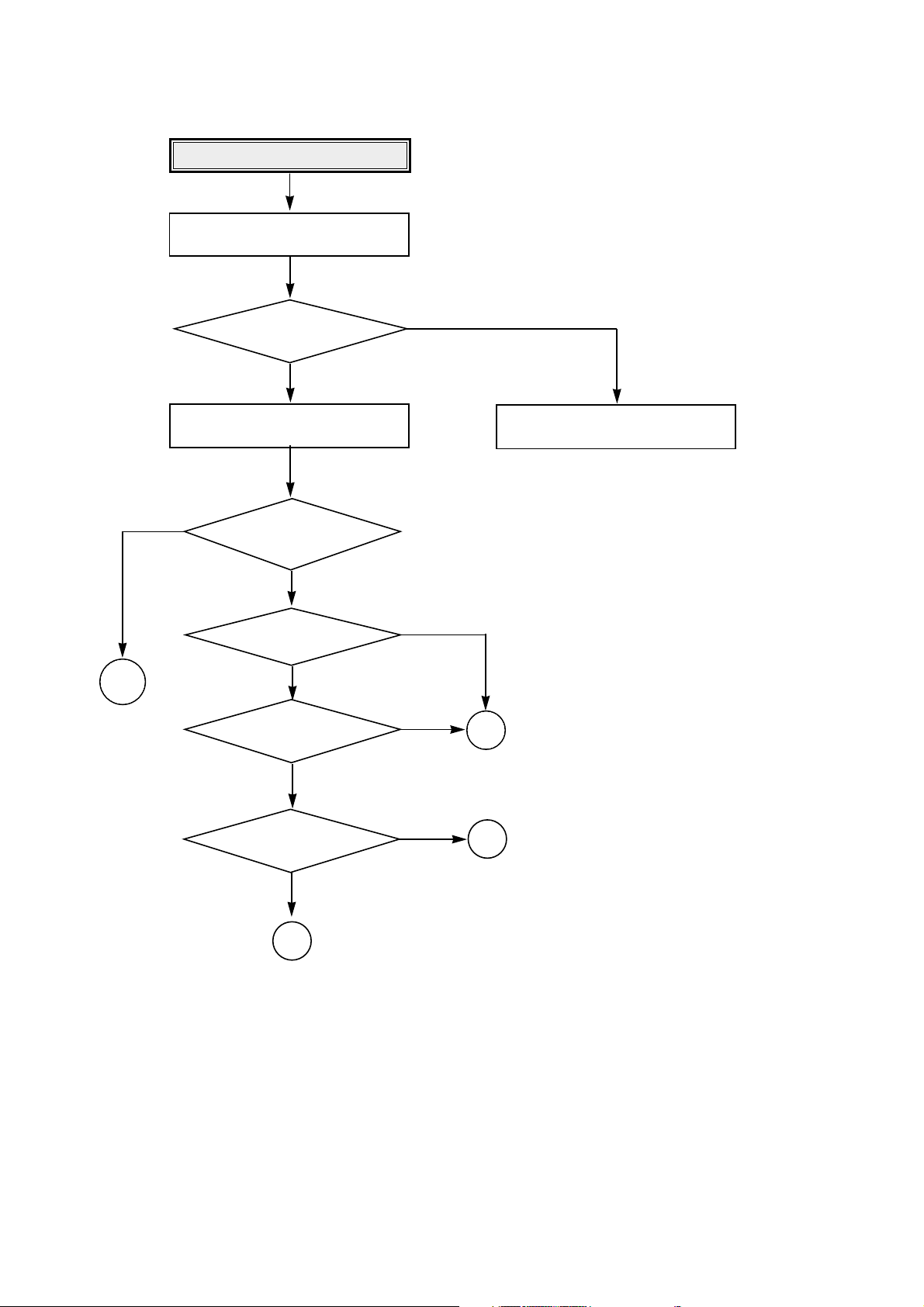
62
In case of writing fail.
Normal Case
Check disc Label.
Finalized Disc?
Check the Media CD-R or
CD-RW?
If CD-R disc, use new CD-R disc.
If CD-RW disc, erase the disc.
Go to “Writing Part Check”
YES
NO
Remove the Dust, Fingerprint and
if the disc has long width
Scratch, change it.
Does the disc
have any Dust, Scratch,
Fingerprint...?
YES
NO
Use LG bundle Software
(Write Tool & Version)
- Easy CD Creator 3.5c
Direct CD 2.5d...
Is the write Tool(version)
supported by LG CD-RW
Drive?
YES
NO
NO
Check disc information on Writng Tool.
[If you get some data information with
“Non Recordable Disc” Message, the
disc is finalized -Finalized Disc :
unrecordable Disc any more]
Eject Disc.
YES
Page 22
63
Writing Part Check.
Refer “Laser is abnormal”.
Load tray with CD-R/RW Disc.
Run the Writing Tool
(Easy CD Creator).
Run the Writing with Tool
(Easy CD Creator).
Go to “ALPC Logic Circuit Check”.
Go to “BETA Measurement
Circuit Check”.
NO
NO
NO
NO
YES
Does Writing finish without
any error?
Is the written file read
normally?
Is the re-written file readed
normally?
Is ROPCSH input signal
Pulse when CD-R writing?
(IC401 pin 43)
The blink
alternates between LED1 and
LED2 when Writing start (OPC
operation)?
Do the IC301(MICOM)
pin 2 and pin 7 output toggle
signals during Writing?
•
Check the connection between
IC301 pin 2, 7 and LED.
•
Check and replace the
LED803, 804.
YES
YES
YES
YES
YES
NO
NO
• Check the communication lines
between IC301 and IC201.
• Check and replace the IC301.
Eject Tray.
Check the connection of IC201 pin 187
and replace the IC201.
OK
Page 23

64
Dragon : Execute LD ‘Off’ Dragon : Execute ‘LD Off’
ALPC Logic Circuit Check.
• Check the connection of IC301 pin 20.
• Check and replace the IC301.
• Check the connection of IC301 pin 14.
• Check and replace the IC301.
•
Check the connection of IC201 pin 166.
•
Check and replace the IC201.
•
Check the connection of IC601 pin 13.
•
Check and replace the IC601.
Execute ‘E. LD On’ of ‘How to
use Test Tool(Dragon)’ :
‘CD-R Recording Mode’
NO
IC601 Pin 33 (CDR/RW) = ‘H’?
IC601 Pin 34(WR/RE) = ‘H’?
IC601 Pin 27(WGATE) = ‘H’?
IC401 Pin 50(WLDON) = ‘H’?
NO
NO
NO
•
Check the connection lines of IC201.
•
Check and replace the IC201.
Are IC601
pin 29(EFM1), 30(EFM2),
42(RESAMP1), 2(RESAMP2),
41(ROPC1) pulse
signals?
NO
•
Check the connection lines of
IC601 pin 21, 18.
•
Check and replace the IC601.
Are PN401 pin 30 (ODON),
31(W/XR) pulse signals?
NO
•
Check the connection lines of IC601.
•
Check and replace the IC601.
Are IC401
pin38(WFPDSH), 39(RFPDSH),
40(WBLSH), 41(SPDSH),
42(MPDSH) pulse
signals?
NO
YES
YES
YES
YES
YES
YES
YES
K
Page 24

65
Dragon : Execute LD ‘Off’
Dragon : Execute LD ‘Off’
• Check the connection of IC301 pin 20.
• Check and replace the IC301.
• Check the connection of IC301 pin 14.
• Check and replace the IC301.
•
Check the connection of IC201 pin
166.
•
Check and replace the IC201.
Execute ‘E. LD On’ of ‘How to use
Test Tool (Dragon)’ :
‘CD-RW Recording Mode’
NO
IC601 Pin 33(CDR/RW): ‘L’?
IC601 Pin 34 (WR/RE) : ‘H’?
IC601 Pin 27(WGATE) : ‘H’?
NO
NO
•
Check the connection of IC601 pin
13.
•
Check and replace the IC601.
IC401 Pin 50(WLDON) : ‘H’?
NO
•
Check the connection lines of
IC601.
•
Check and replace IC601.
Are IC401
pin 38(WFPDSH), 39(RFPDSH),
40(WBLSH), 41(SPDSH), 42(MPDSH)
pulse signals?
NO
• Check the connection lines of IC201.
• Check and replace IC201.
Are IC601
pin 29(EFM1), 30(EFM2),
42(RESAMP1), 2(RESAMP2),
41(ROPC1) pulse signals?
NO
YES
YES
YES
YES
YES
YES
•
Check the connection of IC601 pin
21, 18.
•
Check and replace the IC601.
Are IC401 pin 30(ODON),
41(W/XR) pulse signals?
NO
YES
K
Normal
Page 25

66
BETA Measurement Circuit Check.
• Check the connection of IC401 pin 86.
• Check and replace the IC401(CXA2551R).
• Check the connection of IC301 pin 20.
• Check and replace the IC301(MICOM).
After inserting Test Disc
(TCD-784), 1x play.
NO
IC401 Pin 86(RRF) : 3+/-1.0V?
IC301 Pin 78(RFBETA) : 2+/-1.0V?
IC405 Pin 10 (CDR/RW) : ‘H’?
NO
• Check the connection of IC407.
• Check and replace the IC407.
RRFIN: 2+/0.7V?
(IC401 PIN85)
NO
NO
YES
YES
YES
Is BETA signal normal?
(IC405 pin 14)
NO
YES
• Check the connection of IC401
pin 82.
• Check and replace the IC401.
YES
Check and replace the IC405(BU4052)
Normal
Page 26

67
No audio output
• Check and replace the IC301.
• Check and replace the IC201.
•
Check the connection of L/R OUT.
Insert the audio Disc.
Adjust H/P volume max. (VR801)
NO
AUD_MUTE : ‘L’?
(IC301 Pin 8)
Do LOUT, ROUT signals output?
(IC201 Pin 151, 154)
Do audio Line signals output?
(PN201 Pin51, 54)
NO
NO
•
Check and replace the JK801.
Does the audio
signal output at the headphone
jack(JK801)?
NO
•
Check and replace the IC801.
Do audio signals output?
(IC801 Pin1,7)
NO
YES
YES
YES
YES
YES
Normal
Page 27

68
In case of audio play switch
not working.
• Check the connection of IC301 pin51.
• Replace the IC301.
• Check the connection of SW801.
• Replace SW801.
Replace the IC301.
NO
Is IC301 pin 51 5V before pushing
PLAY KEY (SW801)?
Is IC301 Pin 51 0V pushing
the SW801?
NO
YES
YES
Page 28

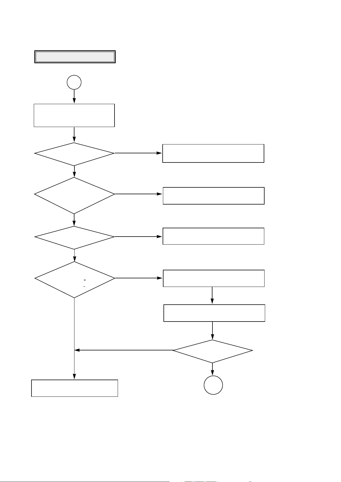
ATIP Absolute Time in Pre-groove. With an additional modulation of the “Wobble”, the “Groove” contains a time
code information.
Wobble The pre-groove in the Disc is not a perfect spiral but is wobbled.
With : – A typical amplitude of 30 nm
– A spatial peried of 54~64 µm
CW Continuous Wave. The laser light output is at a constant level.
DOW Direct Over-Write. The action in which new information is recored over previously recorded information in
CD-RW disc.
Overwrite
The action in which new information is recorded over previously recorded information.
(Pre-)Groove
The guidance track in which clocking and time code information is stored by means of an FM
modulated wobble.
Land Land is characterized in the following way:
When radial signals are concerned,land is defined as the area between the grooves.
When HF signal are concerned,land is defined as the area between the marks(pits) in tangential
direction.
Hybrid Disc A Multisession disc of which the first Session is mastered. On a hybrid disc, recorded and
mastered information may co-exist.
Mastered Information,stored as pits on the disc during the manufacturing process of the disc.
Information (when making the master)
OPC Optimum Power Control. Procedure is determined optimum recording power according to CD-
R/RW Media in recording start step.
ROPC Running OPC. The purpose is to continuously adjust the writing power to the optimum power
that is required.
When the optimum power may change because of changed conditions of disc and change in
operating temperature.
Jitter The 16 value of the time variation between leading and trailing edges of a specific (I3 … I11) pit
or land as measured by Time Interval Analysis.
Deviation The difference between a fixed value of Pit length and Land length.
TOC Table Of Contents : in the Lead-in Area the subcode Q-channel contains information about the
Tracks on the disc.
Packet A method of writing data on a CD in small increments.
Writing Two kinds of packets can be written : Fixed-length and Variable-length.
Write The shape of the HF write signal used to modulate the power of the laser.
Strategy The Write Strategy must be used for recordings necessary for disc measurements.
Information Wobble, ATIP, Disc Identification, Write Power, Speed Range OPC Parameters, etc are
Area recorded in the Information area of CD-RW Disc
Finalization The action in which (partially) unrecorded or logically erased tracks are finished and the Lead-in
and/or Lead-out areas are recorded or overwritten with the appropriate TOC subcode.
Logical Erase
A method to remove information from a disc area by overwriting it with an EFM signal containing
mode 0 subcode
A logically erased area is equivalent to an unrecorded
Physical Erase
The action in which previously recorded information is erased by overwriting with a CW laser
output.
After a Physical Erase action, the erased area on the CD-RW disc is in the unrecorded state
again.
Session
An area on the disc consisting of a Lead-in area, a Program area, a lead-out area.
Multi session
A session that contains or can contain more than one session composed Lead-in and Lead-out
GLOSSARY
10
Page 29

The differences of CD-R/CD-RW discs and General CD-ROM
1. Recording Layer
Recordable CD has a wobbled pre-groove on the surface of disc for laser beam to follow track.
2. Disc Specification
Read-only Disc
CD-R and CD-RW Disc
3~11T
1.6um
0.4~0.5 um
(Pit)Groove
Land
Track pitch(p)
Radial Direction
Iw
A
O
a
a
Groove
Land
Radial Error Signal
The Groove wobble
Average center
Actual center
CD-ROM CD-R CD-RW
Standard Yellow Book Orange Book II Orange Book III
Record Not available Write once Re-writable
I 11/Itop
> 0.6 > 0.6 0.55 > M11> 0.70
(HF Modulation)
Write Laser Power(mW) 4-15 mW 6-14 mW
Read Laser Power(mW) < 0.5 mW < 0.7 mW < 1.0 mW
Jitter < 35 nsec < 35 nsec < 35 nsec
Reflectivity (R
top) 70 % 65 % 15 % ~ 25 %
15
CD-ROM (READ-ONLY DISC)
a=30nm
Page 30

16
3. Disc Materials
1) CD-ROM disc
Laser Beam
Groove
Substrate
(Polycarbonate)
Organic Dye Layer
Reflective Layer
Protective Layer
Label Printing
2) CD-R disc
Pigment Reflective Layer Color
Phtalocyanine Gold/Silver Yellow/White
Cyanine Gold/Silver Dark Green/Bright Green
Azo Gold/Silver Dark Blue
• It is composed of Silver _ colored aluminum plate and Reflective layer.
• Groove (Pit) of aluminum plate make a track.
• Laser wavelength : 780 nm, Laser Power (Read): 0.5mW
• Signal is detected by the
difference of reflective beam
intensity between “pit” and
“Land” on the disc.
• It is so-called WORM (Write Once Read Many) CD.
• It is composed of polycarbonate layer, Organic dye layer, Reflective layer, and Protective
layer.Gold/Silver Reflective layer is used to enhance the reflectivity
• According to the kinds of Organic dye layer, it is divided by Green CD, Gold CD, Blue CD.
• Laser Wavelength : 780 nm, Laser Power (read) : 0.7 mW
• Recording Power : 1x(4~8mW), 2x(8~10mW), 4x(10~13mW), 6x(12~15mW).
• When some part of dye layer is exposed to laser heat, it’s color changs black.Therefore, writing and
reading is enabled by the difference of reflectivity between changed part and unchanged part.
• Polycarbonate layer has Pre_Groove which make a Track.
Laser Beam
Pit
Substrate
(Polycarbonate)
Reflective Layer
Protective Layer
Label Printing
Page 31

17
3) CD-RW Disc
4.
Reading process of Optical Disc
Laser Beam
Groove
Substrate
(Polycarbonate)
Reflective Layer
Dielectric Layer(TL)
Dielectric Layer(UL)
Protective Layer
Label Printing
• It is composed of polycarbonate layer, alloy(silver, arsenic) layer, aluminum reflectivity layer, protective layer.
• An crystalized alloy layer is transformed into noncrystalized by the laser heat. Therefore, writing and reading
is enabled by the difference of reflectivity.
• It is possible to overwrite about 1000 times.
• Laser Wavelength : 780 nm, Laser Power (Read) : 1.0mW
• Recording Power : Erase (4~8mW), Write (12~16mW)
• When disc rewriting, new data is overwritten previously recorded data.
• Polycarbonate layer has a Pre-Groove which make a track.
Lens
H
D
Beam
Spot
Focusing
Lens
Laser Spot
at Constant
Read Intensity
Reflected
Light
Signal
Laser Spot
Position
(Time)
Previously Recorded Marks
Groove Land Mirror
I
3
I
top
I
11
I
G
I
L
I
0
Numerical aperture: NA=nsinθ,
n: Refractive index
Focus depth : H =
λ
/NA
laser spot diameter : D =
λ
/NA
2
θ
Page 32

18
5. Writing Process of CD-R Disc
a b c d e f g
a
b
c
d
e
f
g
Incident
Laser
Powe r
(Read)
(Read)
(Write)
Laser Spot
Position
(Time)
a b c d e f g
Laser Spot
Position
(Time)
Laser
Spot
Recorded
Mark
Reflected
Light
Signal
Reflected
Light
Signal
Below "ORP"– Mark Too Short
At Optimum Record Power ("ORP")
Above "ORP" – Mark Too Long
Time
6. Writing process of CD-RW Disc
Write Power
Erase Power
Read Power
Groove
Crystal
Amorphous
Amorphous
Recorded state
(lower reflectivity)
Melting/
quenching
Heating/
gradual cooling
Crystal phase
Erased state
(higher reflectivity)
Page 33

7. Organization of the PCA, PMA and Lead-in Area
1) Layout of CD-ROM disc
19
Center hole Clamping and Label Area Information Area
Lead-in Area
Lead-in Area
Diameter 15 mm
Diameter 46 mm
Diameter 120 mm
Program Area
Read Only Disc
Lead-out Area
Program Area Lead-out Area
Center hole
Clamping and Label Area
Information Area
PCA PMA
Test Area Count Area
Diameter 15 mm
Diameter 45 mm
Diameter 120 mm
Unrecorded Disc
Tsl-00:35:65 Tsl-00:15:05
Tsl-00:13:25
Tsl
99:59:74
00:00:00
in out
Test Area : for performing OPC procedures.
Count Area : to find the usable area immediately in T.A
Tsl : start time of the Lead-in Area, as encoded in ATIP
PMA : Program Memory Area
Disc Center
Disc Center
2) Layout of CD-R/RW disc
Page 34

20
8. Function of PCA and PMA area
1) PCA (Power Calibration Area)
• PCA area is used to determine the correct Laser Power for a disc.
– Method 1 : PCA area is divided by a track.
– Method 2 : The previous Calibration value is referred.
– Method 3 : ROPC is used to determine Laser Power value automatically in data writing.
• CD-R Disc can write maximum 99 Tracks but CD-RW Disc can write unlimited tracks because it has a rewritable
function.
2) PMA (Program Memory Area)
• It has a track information (track No, track Start/End time) of every track before writing completed.
– PMA area has the last written point and the next writable point of a disc.
– In case of CD to CD copy, some writer may not write PMA area.
* When Disc is Finalized,
PMA information is transferred to the Lead_In area so that general Driver can read it.
* Because PCA and PMA area exist before Lead-In area, General CD Player or CD-ROM Drive can’t read
these areas.
9. OPC and ROPC
1) OPC (Optimum Power Control)
• This is the first step of writing process, because CD writer has its own laser power value and media have different
writing characteristics,
– This is determined by the Writing characteristic, speed, temperature, and humidity.
– Laser wavelength is determined by the environmental temperature (775~795nm) and Optical Laser Power is
determined by the test and retry.
• Asymmetry and optimum writing Power
– EFM signal Asymmetry is determined by the writing power.
Therefore, Optical Power which has the same value to the preset power value can be estimated by measuring
HF signal Asymmetry on the PCA area.
• Measurement of Asymmetry
* Parameter setting (Beta) : Using AC coupled HF signal before equalization
Beta = (A1+A2)/(A1-A2)
Time
P << Po
Time
P = Po
HF Signal
A1
0
A2
Time
P >> Po
Page 35

2) ROPC (Running Optimum Power Control)
• Variable primary factor of Optimum Power
– Change of Power sensitivity on the Disc. (limited to 0.05 *Po)
– Wavelength shift of the laser diode due to the operating temperature change.
– Change of the Spot aberration due to the Disc skew,
Substrate thickness, Defocus.
– Change of Disc or Optics conditions due to the long term OPC
==> It is necessary to adjust continuously to obtain the Optimum Power.
• Principle of Running OPC
– To meet the factors mentioned above,
a horizontal _ direction movement of a curve is uesd.
– Beta = f(B-level) = constant on the Recorded Disc
– Procedure of ROPC
a. Reference B-level is determined during OPC Procedure.
b. During Recording, B-level value is controlled to have a close
Reference B-level value.
c. Normalization of B-level is used to eliminate the effect of reflectivity fluctuation.
==> The reflected B-level value is normalized by the disc reflectivity itself.
21
CD-R/RW Media
Write Strategy
Determination
PCA Test Area
Program Area
PMA Area
Lead-In Area
Lead-out Area
OPC
PCA Count Area
ROPC
* Recording Capacity of CD-R/RW (74Minute Recording media)
• (2048 Byte/Sector) X (75 Sector/Second) X (60 Second/Minute) X 74 Minute
= 681,984,000 Bytes = 682 Mbytes
• But the actual recording capacity is about 650 Mbytes. (according to the ISO 9660 standard, approximately
30 Mbytes are used to make directory structure and volume names.)
Incident recording pulse
Reflected recording pulse
Sampled timing B
11T
Sample B-level (Write Power)
Level B
Sampled at timing B
Pwo decided by OPC
Recording Power
Level B with Pwo
normalized to recording power
Sample Disc Reflectivity
(Read power)
10. Writing Process of DISC
Page 36

INTERNAL STRUCTURE OF THE PICK-UP
1. Connection diagram of the Pick-up
22
1
2
3
4
5
6
12
11
10
9
8
7
C2
C1
VCC
H
A
B
F
Vc
GND
G
D
C
E
GND
IC1
1
2
3
4
5
6
7
8
9
10
11
12
13
14
15
16
17
18
19
20
21
22
23
24
25
26
27
28
29
30
31
32
FCS -
TRK -
TRK +
FCS +
FGND
PDGND
F
B
A
H
PDVcc
PDVc
G
D
C
E
-
FPDVc
FPDO
Vcc
Vcc
CFREQ
CMOD
PGND
VRDC
VWDC2
VWDC1
GND
OSCEN
WE2
WE1
ENBL
2 Axis Actuator
C5
C4
R3
R6
R2
R1
C6
C7
Q1
S
G
D
1
2
3
4
5
6
7
8
16
15
14
13
12
11
10
9
R5
C3
FPD
A
C
Q2
D
S
G
R4
LD
C8
R7
R8
R9
L3
L2
L1
C9
VOUT
VREF
IINR
RFREQ
IIN2
IIN3
OUTEN2
OUTEN3
PDIN
Vcc
IOUT
GND
RAMP
ENBLE
OSCEN
Vcc
IC2
*KRS-202A : CED-8080B’S
*KRS-220C : CED-8083B’S
Page 37

2. Pin Description
23
Pin No. Symbol I/O Function
1 FCS- I Focus coil-
2 TRK- I Tracking coil-
3 TRK+ I Tracking coil +
4 FCS+ I Focus coil +
5FGND
_
Frame GND
6 PGND
_
PDIC GND
7 F O PDIC F OUT
8 B O PDIC B OUT
9 A O PDIC A OUT
10 H O PDIC H OUT
11 VCC I PDIC VCC
12 VC I PDIC VC
13 G O PDIC G OUT
14 D O PDIC D OUT
15 C O PDIC C OUT
16 E O PDIC E OUT
17
18 FPDVC I LD Power Monitor Amp VC
19 FPDO O LD Power Monitor Amp Out
20 Vcc (5V) I LD Analog Voltage +5V
21 Vcc (5V) I LD Analog Voltage +5V
22 CFREQ I Change Frequency
23 CMOD I Change Modulation
24 PGND
_
LD Power GND
25 VRDC I Read Power Analog Control Voltage Input
26 VWDC 2 I Overdrive Analog Control Voltage Input
27 VWDC 1 I Overdrive Analog Control Voltage Input
28 GND
_
LD GND
29 OSCEN I Module Control SW L : off, H : on
30 WE2 I Write Enable 2 L : Write 2 ON
31 WE1 I Write Enable 1 L : Write 1 ON
32 ENBL I LD Drive Current OFF SW, L : LD off
Page 38

3. Signal detection of the P/U
1) Focus Error Signal ==> (A+C)-(B+D)
This signal is generated in RF IC (IC401 : CXA2551R) and controls the pick-up’s up and down to focus on
Disc.
2) Tracking Error Signal (DPP Method) ==> {(A+D)-(B+C)}- kx {(F+H)-(E+G)}
This signal is generated in RF IC (IC401 : CXA2551R) and controls the pick-up’s left and right shift to find
to track on Disc.
3) RF Signal ==> (A+B+C+D)
This signal is converted to DATA signal in DSP IC (IC201 : OTI-9790).
24
Pick-Up module
Photo Diode
Tracking
Focusing
Infrared Iaser
k[(F+H) - (E+G)]
(A+D) - (B+C)
(A+D) - (B+C) - k[(F+H) - (E+G)]
Offset
TE
Tp
Sub2
Main
Tp/2
Sub1
Track Center
F, E
D,C
A,B
H,G
Page 39

DESCRIPTION OF CIRCUIT
1. ALPC (Automatic Laser Power Control) Circuit
1-1. ALPC Loop Circuit
25
+
-
+
-
+
-
+
-
+
-
+
-
P/U
(PN401)
VWDC1
VWDC2
R472
C459
3
13
14
12
9
6
10
5
7
8
19
14
50
38
11
395
6
13
17
16
418 19
C445
R474
R476
R471
C446
R404
R475
IC409
(M62352)
R441
C443
Q401
Q403
ERGCNT
FPDO
VRDC
19
25
27
26
R413
C427
Q404
C422
Q405
W LDON
Q402
R438
5V
RFPDSH
FPDG
Gain
Adj
S/H
S/H
20K
20K
20K
20K
20K
10K
20K
10K
10K
20K
20K
5K
5K
10K
APCCSW
VWDCN
WREF
IC401(CXA2551R)
RREF
VRDC
VRDCN
RLDON
(Read)
(Write)
9K
H:ON
L:OFF
IVON
WLDON
WFPDSH
FPDVC
IC601
(CPLD)
-8~+7.75dB
0.25db Step
H: ON
L: OFF
FPAO
Page 40

1-2. ALPC (Automatic Laser Power Control) Circuit Operation
This circuit consists of Feedback Loop to maintain light output of the Laser Diode.
Feedback signal, output current from PD (Photo Detector) of P/U, is used to monitor the light power of
Laser Diode.
RREF (Read Reference Voltage) of IC401 (CXA2551R) Pin 12, which is from DAC (IC409) Pin 18, is the
reference level of this Loop Circuit.
* Read Loop
• When playback
VRDC (Pin 14) signal of CXA2551R is output to P/U through Gain Control S/W and drives Laser Diode
during playback.
This S/W Circuit is designed to reduce transition time from CD-RW writing mode to playback mode.
• When writing mode
- CD-R
Three Laser Power Levels, Read, Write and Overwrite, are used to write on CD-R disc, and Read
Level is used to monitor the output laser power.
For stabilizing read loop, the S/H signal (RFPDSH), which sample and hold the Read Level of laser
power in the CD-R writing mode, is input through Pin 39 of CXA2551R.
Hence, S/H circuit makes feedback laser power level constant.
- CD-RW
Three Laser Power Levels, Read, Erase and Write, are used to write on CD-RW disc, and Erase Level
is used, during CD-RW writing, to monitor output laser power.
It is not VRDC but VWDC that is the output signal of the control loop performed by Erase level.
ERGCNT makes ALPC Loop stable when it is changed to playback mode from writing mode.
* Write Loop
For stabilizing Write Loop, the S/H signal (WFPDSH), which sample and hold the Erase Level of laser
power in the CD-RW writing mode, is input through Pin 38 of CXA2551R.
Output voltage of Write Loop, VWDC (Pin 10 of CXA2551R), is protected by the high limit diode
applied to P/U.
In the writing mode, the reference signal of Write Loop is WREF (Pin 3 of IC409) and it is input to Pin 5
of IC401 (CXA2551R).
26
Page 41

2. RF Amplifier Circuit
Block Diagram
27
56
97 98 99
100
92 93
94
95
3
57
71
72
26
FE
IC401Pick up KRS-202A/220C
LPF Offset Adj. Gain Adj.
A,B,C,D
E,F,G,H
VC
GND
VCC
PDIC
4
4
LPF
AAF BPF
EQ AMP
RF
SRF
(A+D)-(B+C)
_
CXA2551R
CE
TE
ATFG
+
_
K
AGC
AGC
Offset Adj.
Slice
Circuit
Gain Adj.
LPF
Offset Adj.
Gain Adj.
Gain Adj.
IC201 132
IC201 197
IC201 163
IC201 198
IC201 204
EQRFN
EQRFP
IC413
Page 42

3. Focus/Tracking/Sled Servo Circuit
3-1. Focus, Tracking & Sled Servo Process
28
Focus, Tracking Serve
Sled control
E
F
C
DBA
G
H
Pick up
A,B,C,D,E,F,G,H
IC401 CXA2551R
A,B,C,D
A,B,C,D
E,F,G,H
Focus Error
FE
TE
FAO
T+ T F
__
F+
TAO
Track Error
Detector
Detector
8
D/A
Level shift
Level shift
Focus, Tracking
Sled Motor
IC501
Driver
BA5983FM
Actuator
Level shift
Hall sensor
Digital EQ
Auto Adj. Circuit
SLED -MOVE
SLO
IC501 Driver BA5983FM
Sled control
signal
IC201
Servo control
OTI9790
FAO
TAO
FE
TE
TE FE
A/D
M
IC502 BA5925FA
4
H1 +
SLD+
SLD-
H1 H2 +
H2 -
Sled Clock
IC301
µ-com
Speed
Detector
Page 43

3-2. Focus Servo
The aim of Focus Servo is to maintain the distance between object lens of P/U and disc surface, so that
the detected RF signals (A, B, C, D) can be maximized.
Focus Servo is based on focus error (FE) signal which is generated from focus error detection block in
CXA2551R (IC401) using Astigmatism Method. Focus gain and path can be changed at the CXA2551R
according to the disc, and the resulting output (FE) is input to Servo IC (IC201, OTI-9790).
FE signal after first amplification in OTI-9790 is A/D converted and input to Digital Equalizer Block, most
important part at the Focus Servo. At the Digital Equalizer, adjustments for Focus Bias and Loop Gain are
performed.
After D/A converted, Focus servo signal is output through FAO port (OTI-9790, Pin 207) and drive Focus
Actuator through the Focus Drive IC (IC501, BA5983FM).
3-3. Tracking Servo
The aim of Tracking Servo is to make laser beam trace the data track on disc. Tracking Error (TE) signal
is generated from tracking error detection block in CXA2551R (IC401) using DPP (Differential Push-Pull)
Method. DPP method uses not only main beam (A, B, C, D) but side beams (E,F and G, H) for correcting
DC offset generated in Push-Pull method.
The remaining procedures of TE signal processing in OTI-9790 is similar to Focus Servo.
After D/A converted, Tracking servo signal is output through TAO port (OTI-9790, Pin 208) and drive
Tracking Actuator through the Tracking Drive IC (IC501, BA5983FM).
3-4. Sled Servo
The working distance of tracking actuator is too short to cover whole disc radius. Sled Servo make PU
move by little and little so that the laser beam keep tracing the data track on disc continuously when
tracking actuator reaches the working limit.
Another function of Sled Servo is to seek a target point on disc, following user commands.
Sled error signal is generated with accumulated tracking error signal (that is DC value of TE), which is
input to Servo IC (OTI-9790, Pin 198).
After compensation in OTI-9790, Sled servo signal is output through SLO (OTI-9790, Pin 3) and drive Sled
Motor via IC501.
Another sled control signal, SLEDMOVE from U-COM (IC301), is used in the seek mode for data access.
SLEDMOVE signal is compared with feedback speed signal via Hall sensor and speed detection
IC502(BA5925FV) so that the sled movement speed can be controlled accurately, and it is possible to
seek data access point very fast.
29
Page 44

4. Spindle Servo Circuit
4-1. Spindle Servo Process
4-2. Spindle Servo
Spindle servo is as followings;
1) CD EFM CLV X8 : CD-DA, Video CD
2) Wobble CLV x2, x4, x8 : Blank area in CD-R, CD-RW
3) CD 15x CAV : CD-DA
4) CD 24x CAV : Recorded area in CD-RW
5) CD 32x CAV : CD-ROM, Recorded area in CD-R
– Spindle Servo is controlled by IC201(OTI-9790) and servo signal is output via DMO(Pin 2).
30
Spindle Servo Process
E
F
A
BDC
G
H
Pick up
IC401 CXA2551
Wobble Signal
Generator
8
6
3
RF
SRF
PLL BLOCK
CD EFM CLV
CAV x32
IC510
BA6664FM
ATIP CLV, FG
IC509
NJM3404AV
SPNFG, SPNREV, SPNON
IC201
OTi9790
IC201
OTi9790
Wobble Signal
Demodulation
Level shift
ATIP CLV Control
IC202
µ-com
Spindle Motor
M
Hall sensor
Page 45

69
A. Start
1. Install CED-8080B(CED-8083B) –> PC Power ON –> Execute Windows.
2. Execute Dragon.exe on Windows (Dragon.exe & dragon.cfg should be on same Directory).
3.
If you use CED-8080B(CED-8083B) “E4 Dragon Ver xxx(E5 Dragon Ver xxx)” will be displayed on the Window.
4. Select Setup/Setup I/F on the menu bar.
5. Select ATAPI I/F and then Click OK(Don’t “Select Transfer Rate”)
6. Select Setup/Target Select on the menu bar.
7. Select Number of Host(#0 or #1) appropriately, then
“CED-8080B(CED-8083B)” displays on “Target Device”
8. Select “CED-8080B(CED-8083B)” on Target Device, and then
Click OK.
B. Check Calibration Data
1. Select Calibration/Calibration on the menu bar.
2. Click Read on Calibration window
–> Calibration Data values display.
3. Check Data Values.
[CED-8080B]
CD-R VRDC DAC : 30~150
VWDC1 : 48~112
VWDC2 : 50~155
VWDC2 Offset : 0~35
[CED-8083B]
CD-R VRDC DAC : 30~150
VWDC1 : 48~150
VWDC2 : 50~120
VWDC2 Offset : 0~35
4. Close Calibration window.
• How to use Test Tool (Dragon)
[I/F Setting window]
[Target Select window]
[Calibration window]
Page 46

C. LD Power Setup (VWDC1 / VWDC2 re-setup)
1. Remove disc on the tray.
2. Select LD Inspection/Laser Power Setup on the menu
bar, and then Laser Power Setup window will appear in
sight.
3. Setup LD Power meter (Frequency : 780nm, Measure
Range : 0.01mW unit).
4. Click VRDC button on the LD Power Setup window.
Pick-up will move outside and Laser beam will be
emitted from LD.
5. Measure LD Power with LD Powermeter. -> Type the result on the
blank.
(If you don’t have LD Powermeter,
Type the P/U value without ‘.’ Down to two places of decimals.
ex) 11.34mW -> 1134)
6. Click VWRDC1 button on the LD Power Setup window and follow
above step 4~5.
7. Click Setup and Setup Result will display with OK or NG.
8. Close LD Power Setup window.
D. LD Inspection(VRDC/VWDC/FPD Level Check)
1. Remove disc on the Tray.
2. Select LD Inspection/Laser Inspection on the menu bar,
and then Laser Power Test Window will appear.
3. Click Trigger button and the result will display with OK or
NG.
4. Close Laser Power Test window.
70
[LD Power Setup window]
[LD Power Test window]
Page 47

71
[LD On window]
E.LD On
1. Remove disc on the Tray.
2. Select LD Inspection/LD ON on the menu bar, and then Laser On window will appear.
3. Select LD ON Mode and Click On button, then LD On.
4. Execute Test (Measure LD Power).
5. Click Off button, then LD Off.
6. Close Laser On window.
* Speed setting is valid on “CD-R Recording Mode” & “CD-RW Recording Mode”.
Continous Laser beam is emitted in the “VRDC Loop Mode”, “VWDC-1 Loop Mode” and “VWDC-2 Mode”,
and Pulse_Type Laser output is emitted in the “CD-R Recording Mode” and “CD-RW Recording Mode”.
Page 48

MAJOR IC INTERNAL BLOCK DIAGRAM AND PIN DESCRIPTION
IC401 (CXA2551R) : RF Signal Processor for CD-R/RW
Block Diagram
31
BH01
PHC1
BHC1
RZC
RECD2
RECD1
BETAOUT
PHC2
BHC2
RRFIN
RRF
GND
MCLK
VCC
WRF
MPP
HIN
GIN
FIN
EIN
HAVC
DIN
CIN
BIN
AIN
WLDON
ERGCNT
SCLK
SDATA
XLAT
DVCC
DGND
ROPCSH
MPDSH
SPDSH
WBLSH
REPDSH
WFPDSH
DSPVCC
BGIREF
VTIREF
VCC
VC
DVC
GND
VCT1
VCT2
CNT_VC
CAV_CNT
ATFG
CEP
CEM
CEO
SWRF
WREF
APCCSW
VWDC1
VWDC2
VWDCN
VWDC
FVREF
RREF
VRDCN
VRDC
VCC
FPDO
FPDIN
GND
SMIN
SMFB
SMOUT
AGC3C
AGC2C
AGC1C
ATFM
PHO1
BHO2
PHO2
EQRFN
EQRFP
SRFO
EFGH
AUX
VCC
MPXOUT
MSPP
RFRPIN
GND
RFRP
RFCT
RFCTC1
RFCTC2
TEINTEFE
TZC
XTOK
XTOR
XTAND
AGCON
1 2 3 4 5 6 7 8 9 10 11 12 13 14 15 16 17 18 19 20 21 22 23 24 25
50
49
48
47
46
45
44
43
42
41
40
39
38
37
36
35
34
33
32
31
30
29
28
27
26
75 74 73 72 71 70 69 68 67 66 65 64 63 62 61 60 59 58 57 56 55 54 53 52 51
76
77
78
79
80
81
82
83
84
85
86
87
88
89
90
91
92
93
94
95
96
97
98
99
100
S/H MATRIX
RFEO
RFRP
MPX
FE TE
REGISTER
PH/BH
BETA
CE
APC
ATIP
BIAS
VC
OPAMP
Page 49

32
• Pin Description
Pin No. Name I/O Pin Description
1 CEP – Center Error Amp Input (+)
2 CEM – Center Error Amp Input (-)
3 CEO O Center Error Amp Output
4 SWRF O Write RF Servo Signal Output (for Running OPC)
5 WREF I Power Sertting Voltage Input for Write APC
6 APCCSW – APC Time Constant Control for Write
7 VWDC1 O VWDC1 Voltage Output
8 VWDC2 O VWDC2 Voltage Output
9 VWDCN – APC Amp Input (-) for Write
10 VWDC O APC Amp Output for Write
11 FVREF I Reference Voltage Input for APC
12 RREF I Power Setting Voltage Input for Read APC
13 VRDCN I APC Amp Input (-) for Read
14 VRDC O APC Amp Output for Read
15
34
VCC I Analog Positive Power Source Pin
67
89
16 FPDO I/O Laser Monitor Output/Laser Monitor Voltage Input
17 FPDIN I Laser Monitor Diode Contact Pin
18
31
GND I Analong Ground Pin
63
87
19 SMIN I OP Amp Input
20 SMFB – OP Amp Input (-)
21 SMOUT O OP Amp Output
22 AGC3C O External CAP Connector Pin for AGC Response Speed Setting
23 AGC2G O External CAP Connector Pin for AGC Response Speed Setting
24 AGC1G O External CAP Connector Pin for AGC Response Speed Setting
25 ATFM O Wobble Signal Output
26 ATFG O ATIP FG Output
27 CAV_CNT I CAV Speed Control Voltage Input
28 CNT_VC I CAV Speed Control Reference Voltage Input
29 VCT2 – Decoupling Pin for VC Voltage
30 VCT1 – Decoupling Pin for DVC Voltage
32 DVC O DSPVCC/2 Voltage Output. Internal Reference Voltage.
33 VC O VCC/2 Voltage Output. Internal Reference Voltage.
35 VTIREF – Resistance Connector Pin for Reference Current Setting
36 BGIREF – Resistance Connector Pin for Reference Current Setting
37 DSPVCC I DSP Positive Power Source Pin
38 WFPDSH I Sample Pulse Input for Write APC
Page 50

33
Pin No. Name I/O
Pin Description
39
RFPDSH
I Sample Pulse Input for Read APC
40 WBLSH I Sample Pulse Input for Wobble Signal
41 SPDSH I Sample Pulse Input for Side Beam Signal
42 MPDSH I Sample Pulse Input for Main Beam Signal
43 ROPCSH I Sample Pulse Input for Running OPC
44 DGND I Digital Ground Pin
45 DVCC I Digital Positive Power Source Pin
46 XLAT I Latch Input for Resister Settings
47 SDATA I Data Input for Resister Settings
48 SCLK I Clock Input for Resister Settings
49 ERGCNT I Gain Control Pin for Erase
50 WLDON I Write LD Control Pin
51 AGCON I AGC Control Pin
52 XTAND O Off-Track Detecition Output
53 XTOR O Tracking Amplitude Detection Pin
54 XTOK O Tracking Amplitude Error Detection Pin
55 TZC O Tracking Zero – Cross Signal Output
56 FE O Focus Error Signal Output
57 TE O Tracking Error Signal Processor
58 TEIN I Input for Tracking Signal Processor
59 RFCTC2 – Recording Area Detection Signal 2
60 RFCTC1 – Recording Area Detection Signal 1
61 RFCT O RFRP Slice Level Output
62 RFRP O Radial Contrast Signal Output
64 RFRPIN I CAP Connector Pin for MSPP
65 MSPP O Main Beam–Side Beam Signal Output
66 MPXOUT O Multiplexer Output for Signal Monitoring
68 AUX I Auxiliary Input Pin for Signal Monitoring
69 EFGH O Side Beam Signal Summing Output
70 SRFO O RF Sample Signal Output
71 EQRFP O RF Equalizer Output
72 EQRFN O RF Equalizer Output
73 PHO2 O RRFIN Signal Peak Hold Output
74 BHO2 O RRFIN Signal Bottom Hold Output
75 PHO1 O RRF Signal Peak Hold Output
76 BHO1 O RRF Signal Bottom Hold Output
77 PHC1 – CAP Connector Pin for RRF Signal Peak Hold
78 BHC1 – CAP Connector Pin for RRF Signal Bottom Hold
79 RZC O RF Zero–Cross Detection Signal Output
80 RECD2 O Recording Area Detection Signal 2
81 RECD1 O Recording Area Detection Signal 1
82 BETAOUT O Output for BETA Measure
Page 51

34
Pin No. Name I/O
Pin Description
83 PHC2 – CAP Connector Pin for RRFIN Signal Peak Hold
84 BHC2 – CAP Connector Pin for RRFIN Signal Bottom Hold
85 RRFIN I CAP Connector Pin for RRF
86 RRF O Read RF Signal Output
88 MCLK I Main Clock Input
90 WRF O Write RF Signal Output
91 MPP O Main Push–Pull Signal Output
92 HIN I Side Beam Signal (H) Input
93 GIN I Side Beam Signal (G) Input
94 FIN I Side Beam Signal (F) Input
95 EIN I Side Beam Signal (E) Input
96 HAVC I Main–Side Beam Signal Reference Voltage Input
97 DIN I Main Beam Signal (D) Input
98 CIN I Main Beam Signal (C) Input
99 BIN I Main Beam Signal (B) Input
100 AIN I Main Beam Signal (A) Input
Page 52

IC201(OTI-9790) : ATAPI Interface, Write and DSP Signal Processor
Block Diagram
35
MONIT
EFMR3
EFMR2
EFMR1
EFM
ASY
PANICIN
ESFS
EEFS
WGATE
HFSW
EFM1…3
WRSMP
EFCK
EFMNT1-4
E11TP
E11TS
RESMP1,2
ROPC1…3
MONIT0
MIO0
MIO1
MIO2
DOUT
MIO3
L
R
WBLIN
XIN
XOUT
C34M
CLKOUT
MON
FGIN
SBRK
REVDET
SLO
FOO
TRO
TC
VREF
2VREF
FE
TEBC
BS
TE
RPBC
RP
RXTXCE
LDON
FLAGA…D
TEST0,1
DMO
PRST#
UAD[7:0]
UALE
UA[15:0]
URDY
UWR#
URD#
UCSO#
UCS1#
UINT0#
UINT1#
SDINT#
CPUTYPE
RD[15:0]
ROE#
RCASL#
RCASH#
RWE#
RRAS0#
RA11/RRAS1#
RA10/RRAS2#
RA9/RRAS3#
RAD[8:0]
HDASP#
HA[2:0]
HPDIAG#
IOCS16#
HIRQ
DMACK#
HIORDY
HRD#
HWR#
HDRQ
HD[15:0]
HRST#
ARST#
CS3FX#
CS1FX#
DPLL
Decoder
VPSET
Register
CIRC
CIRC
4K SRAM
4K SRAM
Encoder
PLL
Audio
ATIP
Demodulator
CLK
Generator
Spindle
Motor
Controller
ASYNC
ASYNC+
MSF
TON Bit
DMCON Bit
0 1
CD-SERVO
Spindle/Focus/Tracking/Sled
Microcontroller
Interface
USB
D+
D-
48MHz
ATAPI
Interface
DRAM
Interface
Buffer
Manager
NXSYNC Bit
nX-1X
1X/2X CLV
34.5744MHz
PLLC0,1
Register
LRCKIN
SDIN
BTCK
C2PO
JBSYNC
DEFS
DSFS
SUBIN
SUBCK
Subcode
Interface
CD-DA
Interface
0
1
Sector
Processor
OTI-9790
PLL
Page 53

• Pin Description
36
Pin No. Pin Name Type
Description
149 XIN I Crystal In : System Clock (33.8688MHz)
148 XOUT O Crystal Out: System Clock
141 CLKOUT O Clock Output
8 C34M O Set to 34.5744MHz
CD ENCODER/DECODER Interface
Pin No. Pin Name Type
Description
168 PANICIN I
S
Panic Input : Write abort Input
132 WBLIN I
S
Wobble In : Wobble Input–Digital Signal
167 HFSW O High Frequency Modulation Switch
166 WGATE O Write Gate
180 WRSMP O Write Level Sample : Sample hold signal of write levels on reading
183 EFM1 O EFM 1 : EFM output
184 EFM2 O EFM 2 : EFM output
185 EFM3 O EFM 3 : EFM output
169
EFMNT1/ EFMNT1 : EFM pit pattern length indicator/
EMFNRZ
O
EFMNRZ : EFM Signal Output
170
EFMNT2/ EFMNT2 : EFM pit pattern length indicator/
69M
O
69M : 69.1488MHz
171 EFMNT3 O EFMNT3 : EFM pit pattern length indicator
172 EFMNT4 O EFMNT4 : EFM pit pattern length indicator
175 E11TP O EFM11T Pit Pattern : EFM11T Pit pattern indicator
176 E11TS O EFM11T Space Pattern : EFM11T Pit pattern indicator
177 EFCK O EFM Bit Clock : EFM bit Clock generated from internal clock in CD encoder
181 RESMP1 O Read Level Sample1 : Sample hold signal of read levels on writing
182 RESMP2 O Read Level Sample2 : Sample hold signal of read levels on writing
186 ROPC1 O
Running OPC1 : Sample hold signal 1 of reflected beam for running OPC during write
187 ROPC2 O
Running OPC2 : Sample hold signal 2 of reflected beam for running OPC during write
188 ROPC3 O
Running OPC3 : Sample hold signal 3 of reflected beam for running OPC during write
133 MONIT0 O Monitor 0 : Test pin controlled by Register 03Eh
179 EEFS O EFm Frame Sync
178 ESFS O Encoder Subcode Frame Sync
Clock
WOBBLE Motor Interface
Pin No. Pin Name Type
Description
6 REVDET I
S
Reverse Detect Motor Drive : Indicates spindle motor is rotating in reverse direction
7 FG I FG IN : HG (tachometer) pulse input
12 MON O Motor Drive On : Enables spindle motor drive
13 SBRK O Short Brake : Stops spindle motor by applying a short pulse to the motor winding
Page 54

37
CD-SERVO Interface
Pin No. Pin Name Type
Description
2 DMO O
A
Spindle Motor Servo Output
3 SLO O
A
Sled Servo Output
207 FOO O
A
Focus Servo Output : Focus servo feedback signal
208 TRO O
A
Tracking Servo Output : Tracking servo feedback signal
194 TEBC O
A
Tracking Error Balance Control
197 FE I
A
Focus Error
198 TE I
A
Tracking Error
201 BS I
A
Beam Strength : This input from the preamplifier is the sum of the E and F
photodiode outputs when using a 3-beam pick-up
202 RPBC O
A
Ripple Balance Control
203 RP I
A
Ripple of RF
191 RX I
S
RP Zero Crossing : Used for fine search
192 TX I
S
TE Zero Crossing : Track crossing signal input used in conjunction with RX to
perform fine searches
204 CE I
A
Center Position Error
142 LDON O Laser Diode On
193 TC I
S
Track Count Input : High-frequency track crossing signal input used to perfrom
rough searches and to increment the internal track counter.
137 FLAGA O Servo Monitor Flag A : FLAGA is used to output one of four internal servo signals.
FLAGA can also be used as a general output port.
138 FLAGB O Servo Monitor Flag B : FLAGA is used to output one of four internal servo signals.
FLAGB can also be used as a general output port.
139 FLAGC O Servo Monitor Flag C : FLAGA is used to output one of four internal servo signals.
FLAGC can also be used as a general output port.
140 FLAGD O Servo Monitor Flag D : FLAGA is used to output one of four internal servo signals.
FLAGD can also be used as a general output port.
CD-DSP PIN
Pin No. Pin Name Type
Description
163 EFM I
A
EFM Analog Data
162 ASY O
A
Asymmetry DAC Output
161 EFMR1 I
A
EFM Analog Data Bias 1
160 EFMR2 I
A
EFM Analog Data Bias 2
159 EFMR3 I
A
EFM Analog Data Bias 3
136 MONIT O
CD-DSP Monitor Output : MONIT is used to output several internal CD-DSP signals
Page 55

38
AUDIO Interface
Pin No. Pin Name Type
Description
143 MIO0 I/O Multi Purpose I/O
144 MIO1 O Multi Purpose I/O
145 MIO2 O Multi Purpose I/O
146 DOUT O
Digital Audio Output : Bi-phase serial audio output that follows the EIAJ CP1201 standard.
147 MIO3 I/O Multi Purpose I/O
151 L O
A
Left Channel Audio Output
154 R O
A
Right Channel Audio Output
Note: MIO3-0 can be programmed to control an external audio DAC.
ATAPI LOCAL BUS Interface
Pin No. Pin Name Type
Description
53 HRST# I
S
ATA Host Reset : ATA drive reset
59 HA2
62 HA1 I
S
ATA Host Address : Address signals/USB 48 MHz clock
60 HA0/48M
72 HD15
76 HD14
78 HD13
80 HD12
82 HD11
86 HD10
88 HD9
90 HD8 I/O
PUB
ATA Host Data Bus/SCSI Controller Data Bus
91 HD7
89 HD6
87 HD5
85 HD4
81 HD3
79 HD2
77 HD1
73 HD0
56 CS1FX#/
USBD- I/O
S
ATA Host Chip Select 1FX, 3FX/
57 CS3FX#/ USB D+, D- differential I/O data
USBD+
64 IOCS16# O
OD
ATA 16-Bit I/O
65 HIRQ I/O ATA Host Interrupt Request/SCSI Controller Interrupt Request
54 HDASP# I/O
PUB
ATA Host Interface
61 HPDIAG# I/O
PUB
ATA Host Interface
71 HDRQ O ATA DMA Request/DMA Acknowledge : ATAPI DMA request
DMA acknowledge when connected to SCSI controller
Page 56

39
Pin No. Pin Name Type
Description
67 DMACK# I/O ATA DMA Acknowledge/DMA Request : ATAPI DMA acknowledge
DMA request when connected to SCSI controller
IORDY/
68 DDMARDY#/ O
TS
ATA Host I/O Ready : I/O channel ready
DSTROBE UDMA : DDMARDY#, device DMA ready; DSTROBE, device data strobe
HRD#/
69 HDMARDY#/ I/O
PUA
ATA Host Read Strobe/SCSI DMA Read Strobe
HSTROBE UDMA : HDMARDY#, host DMA ready; HSTROBE, host data strobe
70 HWR#/ I/O
PUA
ATA Host Write Strobe/SCSI DMA Write Strobe
STOP UDMA : Host stop
131 ARST O
TS
ATAPI Reset
SYSTEM CONTROLLER Interface
Pin No. Pin Name Type
Description
95 PRST# I
S
System Reset : Internal state machines are reset and all registers are set to
default. The assertion and negation signal of PRST# can be ASYNC to XIN but
needs to be longer then 1 XIN, because the signal goes through a de-glitch circuit.
106 UCS0# I
S
Chip Select 0 : Enables access to internal registers
107 UCS1# I
S
Chip Select 1 : Enables access to buffer memory
Read Enable/Data Strobe : Read enable/data strobe input for read
104 URD# I
S
If CPUTYPE = VCC (Intel) – This pin is read enabled.
If CPUTYPE = GND (Motorola) – This pin is data strobe.
Write Enable/Data read Status : Write enable/data read write status input for read
105 UWR# I
S
If CPUTYPE = VCC (Intel) – This pin is write enabled.
If CPUTYPE = GND (Motorola) – This pin is read/write status.
110 URDY I/O
PU
Ready : Data ready
Select use/no use by setting internal registers
When accessing internal registers or buffer memory, this signal is asserted after
fixing driven data.
If no access, this pin is Hi-Z.
Hi-Z status at reset.
113 SDINT# SDINT# : CD-DSP and CD-Servo system input.
112 UINT1# O
PU
System Interrupt Request 1 & 0 : CD-Decoder/-Encoder interrupt Signals
111 UINT0# selected by bits INTSEL4-0 in the INTMODE Register (005h,4-0)
103 UAD7
102 UAD6
101 UAD5 I/O Address and Data : Address and data are multiplexed in the same pin.
100 UAD4 If I/O only data, fix UALE to GND.
99 UAD3 These Signals ARE Hi-Z when chip is reset.
98 UAD2
97 UAD1
96 UAD0
Page 57

40
Pin No. Pin Name Type
Description
123 UA7
124 UA6
125 UA5
126 UA4 I
L
Address : Use these pins if the microcontroller has a separate address and data bus.
127 UA3
128 UA2
129 UA1
130 UA0
115 UA15
116 UA14
117 UA13
118 UA12 I
L
Address : Use these pins when accessing 64 KB buffer memory window.
119 UA11
120 UA10
121 UA9
122 UA8
114 UALE I
S
Address Latch Enable : Use this pin if the microcontroller has multiplexed addess and data bus.
CPU Type Select : Microcontroller type (86 type/68type) select
94 CPUTYPE I
S
VCC = Intel
GND = Motorola
Buffer Memory Interface
Pin No. Pin Name Type
Description
39 RAD11
40 RAD10
41 RAD9
42 RAD8
43 RAD7
44 RDA6 O RAM Addess : Addess for DRAM
45 RAD5 These pins are multiplxed address output
48 RAD4
49 RAD3
50 RAD2
51 RAD1
52 RAD0
20 RD15
21 RD14
24 RD13
25 RD12
26 RD11
27 RD10 I/O
PUA
RAM Data : Data for DRAM
28 RD9 Possible to set bus size (16 bit/8bit) by setting internal registers
29 RD8
14 RD7
15 RD6
Page 58

41
Pin No. Pin Name Type
Description
16 RD5
17 RD4 I/O
PUA
RAM Data : Data for DRAM
18 RD3 Possible to set bus size (16 bit/8bit) by setting internal registers
19 RD2
33 RD1
32 RD0
38 RRAS0# O Row Address Strobe 0 : RAS for DRAM
30 RCASH# O Column Address Strobe High : CAS0 for DRAM – If 16 bit bus is selected, this pin
used by strobe
31 RCASL# O Column Address Strobe Low
37 RWE# I/O Write Enable 0 : WE0 for DRAM
Write strobe of RD [7:0] when 16 bit data bus is selected
36 ROE# I/O Output Enable : OE for DRAM
Power Supply
Pin No. Pin Name
Description
9 VDD5 5 Volts
10, 22, 34, 46, 55,
63, 74, 83, 92, VDD Digital Power 3.3 Volts
108, 134, 173, 189
11, 23, 35, 47, 58,
66, 75, 84, 93, VSS Digital Ground
109, 135, 174, 190
152, 153, 157,
158, 199, 206
AVDD Analog Power 3.3 Volts
1, 150, 155, 156, AVSS Analog Ground
165, 195, 200
164, 196 VREF Reference voltage 2.1 Volts
205 2VREF Reference voltage 4.2 Volts
Page 59

IC301 (HD64F3062) : MICOM
Block Diagram
42
Por t 3
Address bus
Data bus (upper)
Data bus (lower)
H8/300H CPU
Interrupt controller
ROM
RAM
16-bit timer unit
Programmable
timing pattern
controller (TPC)
8-bit timer unit
(mask ROM or
flash memory)
Clock pulse
Por t 6Por t 8
generator
Por t 4
Por t 5
P5 /A
3
19
RESO/FWE*
ø/P6
7
6
LWR/P6
P4 /D
0
0
P4 /D
1
1
P4 /D
2
2
P4 /D
3
3
P4 /D
4
4
P4 /D
5
5
P4 /D
6
6
P4 /D
7
7
P3 /D
0
8
P3 /D
1
9
P3 /D
2
10
P3 /D
3
11
P3 /D
4
12
P3 /D
5
13
P3 /D
6
14
P3 /D
7
15
VSSVSSVSSVSSVSSVSSVCCVCCV
CC
MD
2
MD
1
MD
0
EXTAL
XTAL
STBY
P5 /A
2
18
P5 /A
1
17
P5 /A
0
16
Por t 9
P9 /SCK /IRQ
5
15
P9 /SCK
4
0
P9 /RxD
3
1
P9 /RxD
2
0
P9 /TxD
1
1
P9 /TxD
0
0
Por t 2
P2 /A
7
15
P2 /A
6
14
P2 /A
5
13
P2 /A
4
12
P2 /A
3
11
P2 /A
2
10
P2 /A
1
9
P2 /A
0
8
Por t 1
P1 /A
7
7
P1 /A
6
6
P1 /A
5
5
P1 /A
4
4
P1 /A
3
3
P1 /A
2
2
P1 /A
1
1
P1 /A
0
0
/IRQ
4
Bus controller
Watchdog timer
Serial communication
interface
(SCI) x 2 channels
A/D converter
D/A converter
(WDT)
RES
NMI
5
HWR/P6
4
RD/P6
3
AS/P6
2
BACK/P6
1
BREQ/P6
0
WAIT/P6
40
CS /P8
3
31
ADTRG/CS /IRQ /P8
2
22
CS /IRQ /P8
1
13
CS /IRQ /P8
0
0
IRQ /P8
7
15
TP /PB
6
14
TP /PB
5
13
TP /PB
4
12
TP /PB
3
11
3
4
CS /TMIO /TP /PB
2
10
25
CS /TMO /TP /PB
1
9
1
6
CS /TMIO /TP /PB
0
8
0
7
CS /TMO /TP /PB
7
7
2
20
A /TIOCB /TP /PA
6
6
221
5
5
122
4
4
123
A /TIOCA /TP /PA
A /TICOB /TP /PA
A /TICOA /TP /PA
3
3
0
TCLKD/TIOCB /TP /PA
2
2
0
TCLKC/TIOCA /TP /PA
1
1
00
TCLKB/TP /PA
TCLKA/TP /PA
771
DA /AN /P7
660
DA /AN /P7
55
AN /P7
44
AN /P7
33
AN /P7
22
AN /P7
11
AN /P7
00
AN /P7
REF
V
CCAVSS
AV
Por t A Por t 7Por t B
* Functions as RESO in the mask ROM versions and as FWE in the flash memory version.
Page 60

43
•Pin Description
No. Port Name Assign I/O
Description
1 Vcc Vcc I 5V
2 CS7/TMO0/TP8/PB0 LED2 O LED2 control output
3 CS6/TMIO1/TP9/PB1 /PRST O OTI9790 Reset control output
4 CS5/TMO2/TP10/PB2 /UCS1 O OTI9790 Register Select1
5 CS4/TMIO3/TP11/PB3 /UCS0 O OTI9790 Register Select0
6 TP12/PB4 ADSEL O HALL/Seld Out Select
7 TP13/PB5 LED1 O LED1 control output
8 TP14/PB6 AUD_MUTE O Audio mute output
9 TP15/PB7 FWE_ON O Flash writing enable output
10 RESO/FWE FWE I Flash writing mode setting
11 Vss Vss I GND
12 P90/TxD0 ATIP/EFM O Atip/EFM Select Output
13 P91/TxD1 BTS_TXD O Serial communication transmit
14 P92/RxD0 WR/RD O Write/Read Select output
15 P93/RxD1 BTS_RXD I Serial communication receive
16 IRQ4/SCK0/P94 /SDINT I OTI9790 Servo Interrupt Input
17 IRQ5/SCK1/P95 TP15 O for Test
18 D0/P40 SDATAO O Serial data output
19 D1/P41 SCLK O Interface clock output
20 D2/P42 CDR/RW O CDR/CDRW Select output
21 D3/P43 /EPCS O E2PROM selection
22 Vss Vss I GND
23 D4/P44 /CXACS O CXA2551 interface latch signal output
24 D5/P45 /DACS O D/A interface latch signal output
25 D6/P46 TRAY_Mute O Tray Motor Drive Mute control
26 D7/P48 ACT_MUTE O FCS, TRK, and SLD ON/OFF
27 D8/P30 UAD0 I/O DATA IN / OUT
28 D9/P31 UAD1 I/O DATA IN / OUT
29 D10/P32 UAD2 I/O DATA IN / OUT
30 D11/P33 UAD3 I/O DATA IN / OUT
31 D12/P34 UAD4 I/O DATA IN / OUT
32 D13/P35 UAD5 I/O DATA IN / OUT
33 D14/P36 UAD6 I/O DATA IN / OUT
34 D15/P37 UAD7 I/O DATA IN / OUT
35 Vcc Vcc I 5V
36 A0/P10 UA0 O Address output
37 A1/P11 UA1 O Address output
38 A2/P12 UA2 O Address output
39 A3/P13 UA3 O Address output
40 A4/P14 UA4 O Address output
41 A5/P15 UA5 O Address output
42 A6/P16 UA6 O Address output
43 A7/P17 UA7 O Address output
44 Vss Vss I GND
45 A8/P20 UA8 O Address output
46 A9/P21 /OPEN_SW I Open switch input
47 A10/P22 /LOAD_SW I Load switch input
48 A11/P23 RECD1 I Recording area detection signal input
49 A12/P24 RECD2 I Recording area detection signal input
50 A13/P25 TESTMODE0 I
Test Mode 0
Page 61

44
No. Port Name Assign I/O
Description
51 A14/P26 /PLAY_KEY I Play_key input
52 A15/P27 /EJECT_KEY I Eject_key input
53 A16/P50 XTOR I Tracking error amplitude detection input
54 A17/P51 MA/SL I Master / slave detection input
55 A18/P52 TESTMODE1 I Test Mode 1
56 A19/P53 FLAGB I OTI9790 FLAGB (RFZC) Input
57 Vss Vss I GND
58 P60/WAIT URDY I Data ready input
59 P61/BREQ AGCON O Wobble AGC enable output
60 P62/BACK ROPCON O ROPC Enable output
61 P67/Pi SDATAI I E2PROM data input
62 /STBY /STBY I Standby input
63 /RES /RESET I RESET input
64 NMI NMI I Nonmaskable interrupt input
65 Vss Vss I Ground
66 EXTAL EXTAL I Crystal resonator connection input
67 XTAL XTAL I Crystal resonator connection input
68 Vcc Vcc I 5V
69 P63/AS AS O
70 P64/RD /URD O Data read latch output
71 P65/HWR /UWR O Data write latch output
72 P66/LWR /LWR O
73 MD0 MD0 I Input for setting the operation mode
74 MD1 MD1 I Input for setting the operation mode
75 MD2 MD2 I Input for setting the operation mode
76 AVcc AVcc I Analog 5V
77 Vref VREF I A/D reference input (4V)
78 P70/AN0 ASYM1 I ASYM1/B-Level 0 Analog input
79 P71/AN1 ASYM2 I ASYM2/B-Level 1 Analog input
80 P72/AN2 BETA/Jitter I Beta/Jitter analog input (reserved)
81 P73/AN3 MPXO I Multiplexer input for signal monitoring
82 P74/AN4 HALL/SLDOUT I HALL/SLDOUT Analog input
83 P75/AN5 TP40 I for Test
84 P76/AN6/DA0/Q104 TRKJMP O Track Jump control Analog output
85 P77/AN7/DA1/Q103 SLDMOVE O Sled control Analog output
86 AVss AVss I Analog GND
87 IRQ0/P80 ESFS I Encode subcode frame sync input
88 IRQ1/CS3/P81 UINT0 I OTI9790 Interrupt 0 input
89 IRQ2/CS2/P82 UINT1 I OTI9790 Interrupt 1 input
90 IRQ3/CS1/ADTRIG/P83 ADTRIG I A/D conversion external trigger input
91 CS0/P84 CS0/P84 O NC
92 Vss Vss I GND
93 TP0/TCLKA/PA0 FLAGA I OTI9790 FLAGA (TEZC) input
94 TP1/TCLKB/PA1 SBRK O Spindle Motor Short Brake output
95 TP2/TCLKC/TIOCA0/PA2 SPNFG I Spindle FG signal input
96 TP3/TCLKD/TIOCB0/PA3 OPCING O RRF AC Coupling control output
97 TP4/TIOCA1/A23/PA4 SLDFG I Sled FG signal input
98 TP5/TIOCB1/A22/PA5 SPDON O SPINDLE Start/Stop control output
99 TP6/TIOCA2/A21/PA6 SPN8/12M O 8/12cm Disc control output
100 TP7/TIOCB2/A20/PA7 SPNBOOST O Spindle gain selection output
Page 62

45
20
GND
19
Ao2
18
Ao1 DI
16
CLK
15
LD
14
Do
13
Ao12
12
Ao11
11
Vcc
10
VDD
(VrefU)
9
Ao10
8
Ao9
7
Ao8
6
Ao7
5
Ao6
4
Ao5
3
Ao4
2
Ao3
1
Vss
(VrefL)
12-BIT SHIFT REGISTER
8-BIT
R-2R D-A
8-BIT
R-2R D-A
8-BIT
LATCH
8-BIT
LATCH
BUFFER
OP AMP
ADDRESS
DECODER
D-A
D-A D-A D-A D-A D-A D-A D-A
D-A D-A
LLL
LLLLLLL
1
D0
12 3456
D7 D8
910
D11
4Ch3 5 6 7 8 9 10
12 11Ch2
(12)
(12)
(12)
(8)
17
IC409(M62352GP)
1) The M62352 is an integrated circuit semiconductor of CMOS structure with 12 channels of built-in
D-A converters with output buffer operational amplifiers.
2) Outputs of 12 channels are used for adjustment/control of servo circuits and references.
Block Diagram
Pin No. Pin Name Description
1 Vref- GND
2 AO3 B-level Reference
3 AO4 Write power reference
4 AO5 Write power reference
5 AO6 HAVC Offset
6 AO7 Track SPP Reference
7 AO8 Reserved
8 AO9 Hall Bias
9 AO10 Sled Offset
10 Vref+ 4V
Pin No. Pin Name Description
11 VCC 5V
12 AO11 Tray Control
13 AO12 VWDC protect reference
14 ED Serial data output terminal
15 LD LD terminal input
16 CLK Serial clock input terminal
17 DO Serial data input terminal
18 AO1 Read power reference
19 AO2 VWDC2 Power reference
20 GND GND
• Pin Description
Page 63

46
IC501 (BA5983 FM)
1) It controls the sled movement in track search mode and takes the tray to open/close.
2) It controls the Focus/Tracking Actuator receiving the focus error or tracking error signal from IC201.
Block Diagram
+
-
+
-
+
-
+
-
115
16
17
18
19
20
21
22
23
24
25
26
27
28
2
3
4
5
6
7
Pin No. Pin No.
BIAS IN Bias amplifier input
Driver CH1 positive input
Driver CH1 negative input
Driver CH2 negative input
Driver CH2 negative output
CH3 negative input
CH4 negative input
CH4 positive input
Driver CH2 positive input
Driver CH2 positive output
CH3 positive input
CH4 output
Driver CH1 negative output
Driver CH4 negative output
Driver CH1 positive output
Driver CH4 positive output
Driver CH3 negative output
Driver CH3 positive output
Driver CH1 output
Driver CH2 output
OPIN1(+)
OPIN2(+)
OPIN3(+)
OPIN1(-)
OPIN2(-)
OPIN3(-)
OPIN4(+)
PreVcc PreVcc
OPIN4(-)
OPOUT 1
OPOUT 2
CH3 output
OPOUT 3
OPOUT 4
8
9
10
11
12
13
14
GND GND
CH1~3 standby control
STBY1
PowVcc1 PowVcc (CH1,2)
PowVcc2
STBY2
GND GND
PowVcc (CH3,4)
CH4 standby control
VO2 (-)
VO1 (-)
VO4 (-)
VO2 (+)
VO1(+)
VO4(+)
VO3 (-)
VO3(+)
Pin name
Description Pin name Description
1 2 3 4 5 6 7 8 9 1011121314
-
-
+
-
-
+
-
+
+
-
+
+
-
+
-
+
-
+
-
+
-
+
-
+
10K10K10K
10K
10K
10K
10K 10K
10K 10K
10K
10K 10K
10K
10K
10K
10K
20K
10K
20K
10K
10K
10K
CH1CH2
CH3 CH4
Vcc
Vcc
Vcc
CH1, 2, 3
CH4
28 27 26 25 24 23 22 21 20 19 18 17 16 15
Standby
Standby
LEVEL
SHIFT
LEVEL
SHIFT
LEVEL
SHIFT
LEVEL
SHIFT
• Pin Description
Page 64

47
IC510 (BA6664FM) : Spindle Motor Drive IC
It drives the spindle motor receiving the spindle control signal at IC301 (MICOM) and IC201 (OTI-9790).
2
4
7
8
9
10
28
27
26
25
24
23
22
21
20
19
18
17
16
15
11
12
13
14
TL
TSD
GAIN
CONTROL
Hall 1
Hall 2
Hall 3
Hall Bias
BRAKE MODE
HALL AMP
SHORT BRAKE
P S
A3
A2
A1
H1+
H1-
H2 +
H2 -
H3 +
H3 -
FIN
GND
R
NF
RNF
VM
GSW
VCC
FG
VM
PS
EC
ECR
FR
FG2
SB
CNF
BR
VH
+
-
+
-
+
-
+
+
-
-
+
-
+
-
TORQUE
SENSE AMP
SERVO
SIGNAL
CURRENT
SENSE AMP
VCC
VCC
Vcc
VCC
D
CK
Q
Q
R
DRIVER
GAIN
SWITCH
+
-
Pin No.
1
2
3
4
5
6
7
8
9
10
11
12
13
14
15
16
17
18
19
20
21
22
23
24
25
26
27
28
FIN
Description
N.C.
Output3 for motor
N.C.
Output2 for motor
N.C.
N.C.
Output1 for motor
GND
Positive input for hall input Amp1.
Negative input for hall input Amp1.
Positive input for hall input Amp2.
Negative input for hall input Amp2.
Positive input for hall input Amp3.
Negative input for hall input Amp3.
Hall bias terminal
Brake Mode terminal
Capacitor connection pin for phase compensation
Short brake terminal
3 Phase synthesized FG signal output terminal
Rotation detect signal output terminal
Torque control standard voltage input terminal
Torque control voltage input terminal
START/STOP Switch
FG signal output terminal
Power supply for signal division
Gain Switch
Power supply for driver division
Resistance connection pin for output current sense
GND
Pin Name
N.C.
A
3
N.C.
A
2
N.C.
N.C.
A
1
GND
H
1
+
H
1
-
H
2
+
H
2
-
H
3
+
H
3
-
V
H
BR
C
NF
SB
FG
2
FR
E
CR
E
C
PS
FG
V
CC
GSN
V
M1
R
NF
FIN
Block Diagram
• Pin Description
Page 65

48
1 2 3 4 5 6 7 8 9 10 11 12 13 14
2728 26 25 24 23 22 21 20 19 18 17 16 15
+
-
+
-
+
-
+
+
-
+
-
+
-
+
-
+
-
+
+
-
+
-
+
-
+
-
+
STBY
23K
23K
20K
20K
20K
20K
50K
50K
5K 5K
10K
10K
10K
10K
10K
17K
6.8K
40K
40K
40K
40K
40K
40K
40K
40K
44K
44K
44K
44K
100K
100K
100K
100K
8.2K8.2K
8.2K
8.2K
1K
1K
LOGIC
LEVEL
SHIFT
EDGE
Vcc
IC502 (BA5925FV)
It detects the speed of the moving sled, and transfers the sled control signal from IC201 (OTI-9790) to IC501
(BA5983FM)
Block Diagram
Pin No. Pin Name Description
1 GND GND
2 HA+ Hall Amp A Positive Input
3 HA- Hall Amp A Negative Input
4 A+ Hall Amp A Output
5 CA+ Differential Circuit A Input
6 BIAS_IN Bias Amp Input
7 CB+ Differential Circuit B Input
8 B+ Hall Amp Output
9 HB- Hall Amp B Negative Input
10 HB+ Hall Amp B Positive Input
11 IN1+ OP Amp 1 Positive Input
12 IN1- OP Amp 1 Negative Input
13 OUT1 OP Amp 1 Output
14 STBY Standby Control Pin
Pin No. Pin Name Description
15 IN2+ OP Amp 2 Positive Input
16 IN2- OP Amp 2 Negative Input
17 OUT2 OP Amp 2 Output
18 EDGE Edge Pulse Detect Pin
19 VLO VL Amp Output
20 VL- VL Amp Negative Input
21 VCC VCC
22 HB_IN Hall Bias Input
23 VH+ Hall Bias Positive Output
24 VH- Hall Bias Negative Output
25
SW_CONT
Switch Buffer Amp Output Control Pin
26 SW_OUT
Switch Buffer Amp Output
27 SW_IN1
Switch Buffer Amp Input 1
28 SW_IN2
Switch Buffer Amp Input 2
• Pin Description
Page 66

72
Optical
Pick-up
KRS-202A/220C
Spindle
Motor
FCS
TRK
SLED
Motor
Tray
Motor
Laser
Power
S/H
17.43MHz
RF/Servo Signal
Timing Signals
OPC/ROPC
Circuit
Address/Data
M62352
12ch
8bit DAC
AT93C86
1kB
EEPROM
BA5983FM
F.T.S.T DRIVE
CXA2551R
RF Amp
Wobble
ALPC
CPLD
Laser Control
S/H Signal Gen.
20MHZ
H8/3062
System
Controller
33.86MHz
OTI9790
DSP+Servo
DECODER
ENCODER
ATIP Demodulator
Write Strategy
I/F
Data
2MB
DRAM
H
O
S
T
I/F
Cable
Audio
Mute
H/P Amp
L,R
L,R
Line Out
Headphone
Jack
BA6664FM
MOTOR DRIVE
BA5925
Sled
Speed
BLOCK DIAGRAM
1. Block Diagram of CD-R/RW Drive
Page 67

73
From HOST
PN201
41 42 43 44
+12V
+5V
GND
GND
L101
Bead
L102
Bead
12V
8V
8V
IC512
NJM7808
Regulator
IC511
NJM7808
Regulator
IC501 BA5983
FCS/TRK/SLD/TRY
Driver
Act _Mute
IC201
OTI-9790
DSP/Servo
/ATAPI
/PRST
/UCS0, 1
URDY, URD, UWR
UA[0:8], UAD[0:15]
IC301
HD64F3062
µ-COM
IC101
XC61AN
RESET
IC102
BA033S
Regulator
IC103
BA3939
Regulator
3.3V
4V
(3.9V)
5V
IC401
CXA2551 ASP
2V
IC514
NJM3414
OP Amp
2V_ACT
2.5V
/RESET
/CXACS
SDATA, SCLK
SDATA, SCLK
SDATA, SCLK
/DACS
/EPCS
32
IC302
AT93C86
EEPROM
IC409
M62352
DAC
2. Power Block Diagram
Page 68

74
W/XR, OSCEN,ENBL,ODON
WFPDSH, RFPDSH, WBLSH, SPDSH, MPDSH
A,B,C,D,E,F,G,H
IC401
CXA2551
ASP
MD
HA+/-
H1+/-,H2+/-
TRY+/-
SLD+/-
FCS+/-
TRK+/-
HU,HV,HW
U,V,W
EC
TRY CTL
SLD FG
MPXO
RECD1,2,XTOR
PHO1
RFRP,RFCT
ATFG
CE
TZC
TE
FE
IC403
NJM3404
IC404
NJM2903
IC412
TC7W08
IC414
NC7SZ66
IC403
NJM3404
IC411
NJM3404
EFM1,2,3
WGATE,LDON
EFCK,EEPS
TEBC
TE
TX
CE
WBLIN
RPBC
RX
BS
/UCS0,1,URDY,URD,UWR
UA[0:8],UAD[0:15]
IC301
HD64F3062
µ-COM
SLD_MOV
IC509
BA5925
Sled Speed
IC409
M62352,DAC
IC501
BA5983
Drive
IC510
BA6664
Drive
SPDL FG
DMO
FAO/TAO
SLO
IC601
XC9536
CPLD
IC201
OTI-9790
IC509
NJM3404
IC508
BU4053
3. System Control Block Diagram
Page 69

75
A,B,C,D,E,F,G,H
FPDO
VRDC, VWC1
MD
WREF
RPOWER
VWDC2
IC409
M62352
DAC
/DACS
SDATA,SCLK
BETA,ASYM1,2
BLEBEL0
IC401
CXA2551
ASP
PHO1
RRFIN
RRF
EQRFN,EQRFP
W/XR,OSCEN,ENBL,ODON
WFPDSH,RFPDSH,WBLSH,SPDSH,MPDSH
ERGCNT,WBLON
IC403
NJM3403
IC413
EL2245CS
IC405
BU4052B
IC301
HD64F3062
µ-COM
/UCS0,1,URDY,URD,UWR
UA[0:8],UAD[0:15]
Lout
Line out
Rout
Q804
Mute Control
IC801
H/P Amp
H/P Out
RFDC(1V)
EFM(RFAC)
(1.2V)
BS
IC201
OTI-9790
EFM1,2,3
WGATE,LDON
EFCK,EEPS
IC601
XC9536
CPLD
4. Write/Read Block Diagram
Page 70

76
CXA2551R
RF Amp.
Wobble
ALPC
OTI9790
DSP + Servo
DECODER
ENCODER
ATIP Demodulator
Write Strategy
I/F
33.86MHz
I/F
cable
H
O
S
T
Data
Data
Command
DRAM
CPLD
*Optical
Pick-up
KRS-202A/220C
Disc
Motor unit
GRS-R02A/
OSM-32A
Laser
Control
SPINDLE
MOTOR
FOCUS
COIL
TRACKING
COIL
SLED
MOTOR
LOADING
MOTOR
BA6664FM
MOTOR DRIVE
BA5983FM
F.T.S.F DRIVE
20MHz
Beta
H8/3062
System
Controller
AUDIO
Circuitry
RF
ROPC
Circuit
A1,A2, B Level
Headphone
Jack
R-ch
L-ch
Line-out
+8V
+5V
GND
GND
+12V
+5V
GND
GND
+12V
8V Reg.
3.3V Reg. +3.3V
+3.9V
3.9V Reg.
A B CD
1
2
3
4
5
5. Block Diagram
* CED-8080B : Optical Pick-up KRS-202A
* CED-8083B : Optical Pick-up KRS-220C
Page 71

A B C D E F GH
1
2
3
4
5
435
013
420
431
008
009
012
011
014
004
006
015
016
402
402
402
430
430
021
020
500
024
419
025
020
402
027
026
023
022
402
400
413
413
413
413
021
030
029
007
003
002
031
050
010
402
028
001
PBM00 (MAIN C. B. A)
005
034
A02
A01
11 1 2
EXPLODED VIEW
 Loading...