

LG CE110 Service Manual
Date: October, 2007 / Issue 1.0
Service Manual
Model : CE110
Service Manual
CE110
Internal Use Only

- 3 -
1. Introduction ..................................... 5
2. Performance .................................... 6
2.1 Product Name ......................................... 6
2.2 Supporting Standard................................6
2.3 Main Parts : GSM Solution...................... 6
2.4 HW Feature..............................................7
2.6 Technical Specification ..........................12
3. Circuit Description........................ 17
3.1 General Description .............................. 17
3.2 RF Part.................................................. 17
3.3 Digital Baseband....................................24
3.4 Analog Baseband.................................. 32
3.5 Bluetooth Interface................................ 40
4. TROUBLE SHOOTING .................. 43
4.1 RF Part Technical Brief......................... 43
4.2 RF Part Trouble shooting...................... 49
4.3 Bluetooth Trouble Shooting .................. 56
4.4 Baseband Part Troubleshooting ........... 59
4.5 LCD Display Trouble............................. 66
4.6 Camera Trouble Shooting..................... 71
4.7 SIM Detect Trouble Shooting................ 76
4.8 Slide Up/Down and Trouble Shooting... 79
4.9 Receiver Trouble................................... 81
4.10 MIC Trouble Shooting ......................... 85
4.11 Ear-Mic Jack Detection
Trouble Shooting................................. 87
4.12 Ear-Mic Hook Detection Trouble
Shooting.............................................. 88
4.13 Ear-Mic Headset MIC
Trouble Shooting................................. 89
4.14 Ear-Mic Headset HSOR/HSOL
Trouble Shooting................................. 90
4.15 Main Key Backlight LED Trouble
Shooting.............................................. 91
4.16 Vibrator Trouble Shooting....................93
5. Downloading Software ................. 95
5.1 The purpose of downloading software.. 95
5.2 The Environment of Downloading
Software................................................ 95
5.3 Download Procedure .............................97
6. BLOCK DIAGRAM ....................... 104
7. CIRCUIT DIAGRAM...................... 111
8. BGA Pin Map ............................... 117
9. PCB LAYOUT............................... 121
10. RF Calibration
................................
123
10.1 What’s the Rx Calibration?
..............
123
10.2 What’s the Tx Calibration?
..............
123
10.3 Calibration program - HOT_KIMCHI 124
11. EXPLODED VIEW &
REPLACEMENT PART LIST ..... 129
11.1 EXPLODED VIEW ............................ 129
11.2 Replacement Parts
<Mechanic component>.................... 131
<Main component> ........................... 134
11.3 Accessory ......................................... 147
Table of Contents
LGE Internal Use Only
Copyright © 2007 LG Electronics. Inc. All right reserved.
Only for training and service purposes

LGE Internal Use Only
Copyright © 2007 LG Electronics. Inc. All right reserved.
Only for training and service purposes

- 5 -
1. Introduction
1.1 Purpose
This manual provides the information necessary to repair, calibration, description and download the features of the CE110.
1.2. Regulatory Information
A. Security
Toll fraud, the unauthorized use of telecommunications system by an unauthorized part (for example, persons other than your
company’s employees, agents, subcontractors, or person working on your company’s behalf) can result in substantial
additional charges you’re your telecommunications services. System users are responsible for the security of own system.
There are may be risks of toll fraud associated with your telecommunications system. System users are responsible for
programming and configuring the equipment to prevent unauthorized use. LGE does not warrant that this product is immune
from the above case but will prevent unauthorized use of common-carrier telecommunication service of facilities accessed
through or connected to it. LGE will not be responsible for any charges that result from such unauthorized use.
B. Incidence of Harm
If a telephone company determines that the equipment provided to customer is faulty and possibly causing harm or interruption
in service to the telephone network, it should disconnect telephone service until repair can be done. A telephone company may
temporarily disconnect service as long as repair is not done.
C. Changes in Service
A local telephone company may make changes in its communications facilities or procedure. If these changes could reasonably
be expected to affect the use of the KE820/KG99 or compatibility with the network, the telep hone company is required to give
advanced written notice to the user, allowing the user to take appropriate st eps to maintain telephone service.
D. Maintenance Limitations
Maintenance limitations on the CE110 must be performed only at the LGE or its authorized agents. The user may not make
any changes and/or repairs expect as specifically noted in this manual. Therefore, note that un authorized alternations or
repair may affect the regulatory status of the system and may void any remaining warranty.
E. Notice of Radiated Emissions
The CE110 complies with rules regarding radiation and radio frequency emission as defined by local regulatory agencies. In
accordance with these agencies, you may be required to provide information such as the follo wing to the end user.
F. Pictures
The pictures in this manual are for illustrative purposes only; your actual hardware may look slightly different.
G. Interference and Attenuation
An CE110 may interfere with sensitive laboratory equipment, medical equipment, etc. Interference from unsuppressed engines
or electric motors may cause problems.
H. Electrostatic Sensitive Devices
ATTENTION
Boards, which contains Electrostatic Sensitive Device(ESD), are indicated by the sign. Following information is ESD handling:
Service personnel should ground themselves by usinga wrist strap when exchange system boards.
When repairs are made to a system board, they should spread the floor with anti-static mat which is also grounded. Use a
suitable, grounded soldering iron. Keep sensitive parts in these protective packages until these are used. When returning
system boards or parts such as EEPROM to the factory, use the protective package as described.
1. Introduction
LGE Internal Use Only
Copyright © 2007 LG Electronics. Inc. All right reserved.
Only for training and service purposes
LGE Internal Use Only
Copyright © 2007 LG Electronics. Inc. All right reserved.
Only for training and service purposes
2. Performance
- 6 -
2. Performance
2.1 Product Name
CE110 : GPRS Class 10 / EDGE Class 10
2.2 Supporting Standard
2.3 Main Parts : GSM Solution
Item Feature Comment
Supporting Standard GSM850/DCS1800/PCS1900
with seamless handover
Phase 2+(include AMR)
SIM Toolkit : Class 1,2,3,E
Frequency Range GSM850 TX : 824 - 849 MHz
GSM850 RX : 869 - 894 MHz
DCS1800 TX : 1710 - 1785 MHz
DCS1800 RX : 1805 - 1880 MHz
PCS1900 TX : 1850 - 1910 MHz
PCS1900 RX : 1930 - 1990 MHz
Application Standard WAP 2.0, JAVA 2.0
Item Part Name Comment
Digital Baseband Neptune (D761811BZVL): TI
Analog Baseband Triton (TWL3029): TI
RF Chip B6PLD: RENESAS
- 7 -
2. Performance
2.4 HW Feature
LGE Internal Use Only
Copyright © 2007 LG Electronics. Inc. All right reserved.
Only for training and service purposes
Item Feature Comment
Form Factor Slide
1) Capacity
Battery Standard : Li-Polymer, 900mAh
2) Packing Type : Hard Pack
Size
Standard :
89.5 X 47.0 X 20 mm
Weight 81g With Battery
Volume 68cc
PCB Staggered 8Layers , 0.8t
Stand by time 260 hrs @ Paging Period 5
Charging time 3 hrs @ Power Off / 800mAh
Talk time Min : 3.0 hrs @ Power Level 7 @ EGSM / 800mAh
GSM850 : -105 dBm
RX sensitivity DCS 1800 : -105 dBm
PCS 1900 : -105 dBm
GSM/ GSM850 : 33 dBm Class4 (GSM850)
GPRS DCS 1800 : 30 dBm Class1 (PCS)
TX output power
PCS 1900 : 30 dBm Class1 (DCS)
GSM850 : 27 dBm E2 (EGSM)
EDGE DCS 1800 : 26 dBm E2 (PCS)
PCS 1900 : 26 dBm E2 (DCS)
GPRS compatibility GPRS Class 10
EDGE compatibility EDGE Class 10
SIM card type
Plug-In SIM
3V /1.8V
Main LCD
Display 262K Color TFT (128 x 128)
Backlight : White LED
Built-in Camera VGA Camera One button access
- 8 -
2. Performance
LGE Internal Use Only
Copyright © 2007 LG Electronics. Inc. All right reserved.
Only for training and service purposes
Item Feature Comment
Status Indicator None
Alphanumeric Key : 12 Function Key:
Function Key : 10 4 Key Navigation, OK, F1,
Side Key : 4 F2, CLR, SND
Keypad
Total No of Keys :26 Side Key :
Volume up/down, CAM,
PWR/END
ANT
Main : Internal Fixed Type
Bluetooth : Internal Fixed Type
System connector 18 Pin
Ear Phone Jack 18pin, 4 Pole, Stereo
PC synchronization Yes
Memory
NAND Flash : 512Mbit
SDRAM : 512Mbit
Speech coding FR, EFR, HR,AMR
Data & Fax Built in Data & Fax support
Vibrator Built in Vibrator
Blue Tooth
V2.0, HSP, HFP, OPP, FTP(server),
BPP, A2DP, AVRCP
MIDI
(for Buzzer Function)
SW Decoded 64Poly
Music Player MP3/ AAC/AAC+ With Graphic EQ
Camcorder MPEG4, H.263, H.264
Voice Recording Yes
Speaker Phone mode
Yes
Support
Travel Adapter Yes
CDROM No
Stereo Headset Yes Optional
Data Cable Yes Optional
T-Flash (External Memory)
No Optional
- 9 -
2. Performance
LGE Internal Use Only
Copyright © 2007 LG Electronics. Inc. All right reserved.
Only for training and service purposes
Item Feature Comment
RSSI 0 ~ 4 Levels
Battery Charging 0 ~ 4 Levels
Key Volume 0 ~ 5 Level
Audio Volume 1 ~ 5 Level
Time / Date Display Yes NITZ
Multi-Language Yes English / French/ Spain
Quick Access Mode
Phone Book / Message / Camera
/ My Stuff / Favorite
PC Sync Schedule / Phonebook / MEMO /
SMS / Download(Photo, file)
Speed Dial Yes (2~9) Voice mail center -> 1 key
Profile Yes
CLIP / CLIR Yes (different melody)
Phone Book 4 Numbers + 1 Memo + 1 e-mail + Total 1000 Member
Group Select + Picture
Last Dial Number Yes (40)
Last Received Number Yes (40)
Last Missed Number Yes (40)
Search by Number/Name Name only
Group 7 Possible Rename
Fixed Dial Number Yes
Service Dial Number Yes
Own Number Yes
Voice Memo
Yes
Call Reminder Yes
Network Selection Automatic
Mute Yes
Call Divert Yes
Call Barring Yes
Call Charge (AoC) No No for Cingular
LGE Internal Use Only
Copyright © 2007 LG Electronics. Inc. All right reserved.
Only for training and service purposes
2. Performance
- 10 -
Item Feature Comment
Call Duration Yes
SMS (EMS) 100 (10) EMS : Release4
(Except Text align)
SMS Over GPRS Yes
EMS Melody / Picture Yes
Send / Receive / Save
MMS MPEG4 / Send / Yes
Receive / Save
Long Message MAX 925 Characters
Cell Broadcast Yes
Download Over the WAP
Game YES
Calendar Yes
Memo 50
Unit Convert Currency/Area/Length/Volume/Weight
/Temperature/Velocity
Tip Calculator No
Wall Paper Yes Default 5ea
WAP Browser Over WAP 2.0 Up Brower Obigo Q-line
Download Melody / Yes Over WAP
Wallpaper
SIM Lock Yes Operator Dependent
SIM Toolkit Class 1, 2, 3, A-E
MMS Yes Openwave MMS Client
EONS Yes
CPHS
Yes V4.2
ENS Yes
Camera Yes 2M F/F / Digital Zoom : x4
JAVA Yes CLDC V1.1 / MIDP V2.0
Download Over WAP
Voice Dial No
- 11 -
2. Performance
LGE Internal Use Only
Copyright © 2007 LG Electronics. Inc. All right reserved.
Only for training and service purposes
Item Feature Comment
IrDa No
V2.0
Blue tooth Yes
HSP, HFP, OPP,
FTP(server),
BPP, A2DP, AVRCP
GPRS Yes Class 10
EDGE Yes Class 10
Hold / Retrieve No
Conference Call Yes Max. 6
DTMF Yes
Memo pad Yes
TTY Yes
AMR Yes
Sync ML No
IM Yes
Email Yes
LGE Internal Use Only
Copyright © 2007 LG Electronics. Inc. All right reserved.
Only for training and service purposes
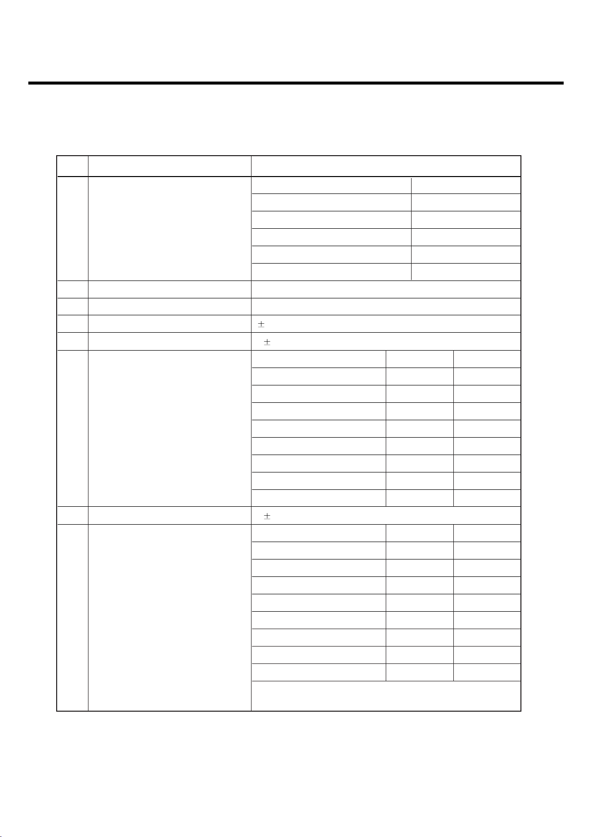
2.6 Technical Specification
2. Performance
- 12 -
Item Description Specification
GSM850
TX: 824 + n x 0.2 MHz (n=1 ~ 124)
RX: TX + 45 MHz
1Frequency Band DCS1800
TX: 1710 + ( n-511 ) x 0.2 MHz (n = 512 ~ 885)
RX: TX + 95 MHz
PCS1900
TX: 1850 + ( n-511 ) x 0.2 MHz
RX: 1930 + ( n-511 ) x 0.2 MHz (n = 512 ~ 810)
2 Phase Error
RMS < 5 degrees
Peak < 20 degrees
3 Frequency Error < 0.1ppm
GSM850
Level Power Toler. Level Power Toler.
5 33 dBm 2dB 13 17 dBm 3dB
6 31 dBm 3dB 14 15 dBm 3dB
7 29 dBm 3dB 15 13 dBm 3dB
8 27 dBm 3dB 16 11 dBm 5dB
9 25 dBm 3dB 17 9 dBm 5dB
10 23 dBm 3dB 18 7 dBm 5dB
11 21 dBm 3dB 19 5 dBm 5dB
4 Power Level 12 19 dBm 3dB
DCS1800/PCS1900
Level Power Toler. Level Power Toler.
0 30 dBm 2dB 8 14 dBm 3dB
1 28 dBm 3dB 9 12 dBm 4dB
2 26 dBm 3dB 10 10 dBm 4dB
3 24 dBm 3dB 11 8 dBm 4dB
4 22 dBm 3dB 12 6 dBm 4dB
5 20 dBm 3dB 13 4 dBm 4dB
6 18 dBm 3dB 14 2 dBm 5dB
7 16 dBm 3dB 15 0 dBm 5dB

LGE Internal Use Only
Copyright © 2007 LG Electronics. Inc. All right reserved.
Only for training and service purposes
2. Performance
- 13 -
Item Description Specification
GSM850
Offset from Carrier (kHz) Max. dBc
100 0.5
200 -30
250 -33
400 -60
600~ <1,200 -60
1,200~ <1,800 -60
1,800~ <3,000 -63
3,000~ <6,000 -65
5
Output RF Spectrum 6,000 -71
(due to modulation) DCS1800/PCS1900
Offset from Carrier (kHz). Max. dBc
100 0.5
200 -30
250 -33
400 -60
600~ <1,200 -60
1,200~ <1,800 -60
1,800~ <3,000 -65
3,000~ <6,000 -65
6,000 -73
GSM850
Offset from Carrier (kHz) Max. (dBm)
Output RF Spectrum 400 -19
6
(due to switching transient) 600 -21
1,200 -21
1,800 -24
LGE Internal Use Only
Copyright © 2007 LG Electronics. Inc. All right reserved.
Only for training and service purposes
2. Performance
- 14 -
Item Description Specification
DCS1800/PCS1900
Offset from Carrier (kHz). Max. (dBm)
Output RF Spectrum 400 -22
6
(due to switching transient) 600 -24
1,200 -24
1,800 -27
7 Spurious Emissions Conduction, Emission Status
8 Bit Error Ratio BER (Class II) < 2.439% @-102dBm
9 Rx Level Report accuracy 3 dB
10 SLR 8 3 dB
Frequency (Hz) Max.(dB) Min.(dB)
100 -12 -
200 0 -
300 0 -12
11 Sending Response 1,000 0 -6
2,000 4 -6
3,000 4 -6
3,400 4 -9
4,000 0 -
12 RLR 2 3 dB
Frequency (Hz) Max.(dB) Min.(dB)
100 -12 -
200 0 -
300 2 -7
500
*
-5
13 Receiving Response 1,000 0 -5
3,000 2 -5
3,400 2 -10
4,000 2
*
Mean that Adopt a straight line in between 300 Hz and
1,000 Hz to be Max. level in the range.
LGE Internal Use Only
Copyright © 2007 LG Electronics. Inc. All right reserved.
Only for training and service purposes
2. Performance
- 15 -
Item Description Specification
14 STMR 13 5 dB
15 Stability Margin > 6 dB
dB to ARL (dB) Level Ratio (dB)
-35 17.5
-30 22.5
-20 30.7
16 Distortion
-10 33.3
0 33.7
7 31.7
10 25.5
17 Side Tone Distortion Three stage distortion < 10%
18
<Change> System frequency
2.5ppm
(13 MHz) tolerance
19 <Change>32.768KHz tolerance 30ppm
Full power
260mA(GSM850), 220mA(DCS/PCS)
20 Power consumption Standby
- Normal mode 4.0mA(Max.power)
- Using Test mode on DSP Sleep function 3mA
GSM850/Lvl 7 (Battery Capacity 900mA) : 200 min
20 Talk Time
GSM850/Lvl 12 (Battery Capacity 900mA) : 320 min
PCS1900/Level5 (Battery 800mA) : 310 Min
PCS1900/Level10(Battery 800mA) : 390 Min
Under conditions, at least 200 hours:
1. Brand new and full 800mAh battery
2. Full charge, no receive/send and keep GSM in idle mode.
21 Standby Time
3. Broadcast set off.
4. Signal strength display set at 3 level above.
5. Backlight of phone set off.
At least 70 dB under below conditions:
22 Ringer Volume 1. Ringer set as ringer.
2. Test distance set as 100 cm
23 Charge Voltage
Fast Charge : < 600 mA
Slow Charge: < 60 mA
LGE Internal Use Only
Copyright © 2007 LG Electronics. Inc. All right reserved.
Only for training and service purposes
2. Performance
- 16 -
Item Description Specification
Antenna Bar Number Power
4 -89 dBm ~
3 -94 dBm ~ -90 dBm
24 Antenna Display
2 -99 dBm ~ -95 dBm
1 -104 dBm ~ -100 dBm
0~ 104 dBm
Barttey Bar Voltage
0(included Blinking) 3.62V~3.33V
1 3.70V ~ 3.63V
25 Battery Indicator
2 3.76V ~ 3.71V
3 3.89V ~ 3.77V
4 4.20V ~ 3.90V
26 Low Voltage Warning
3.60V↓ 0.03V (Standby)
3.50V↓ 0.03V (Call)
27 Forced shut down Voltage 3.35 0.03 V
1 Li-polymer Battery, Hardpack
28 Battery Type
Standard Voltage = 3.7 V
Battery full charge voltage = 4.2 V
Capacity: 900mAh
Switching-mode charger
27 Travel Charger Input: 100 ~ 240 V, 50/60Hz
Output: 5.1V, 700mA
LGE Internal Use Only
Copyright © 2007 LG Electronics. Inc. All right reserved.
Only for training and service purposes
3. Circuit Description
- 17 -
3. Circuit Description
3.1 General Description
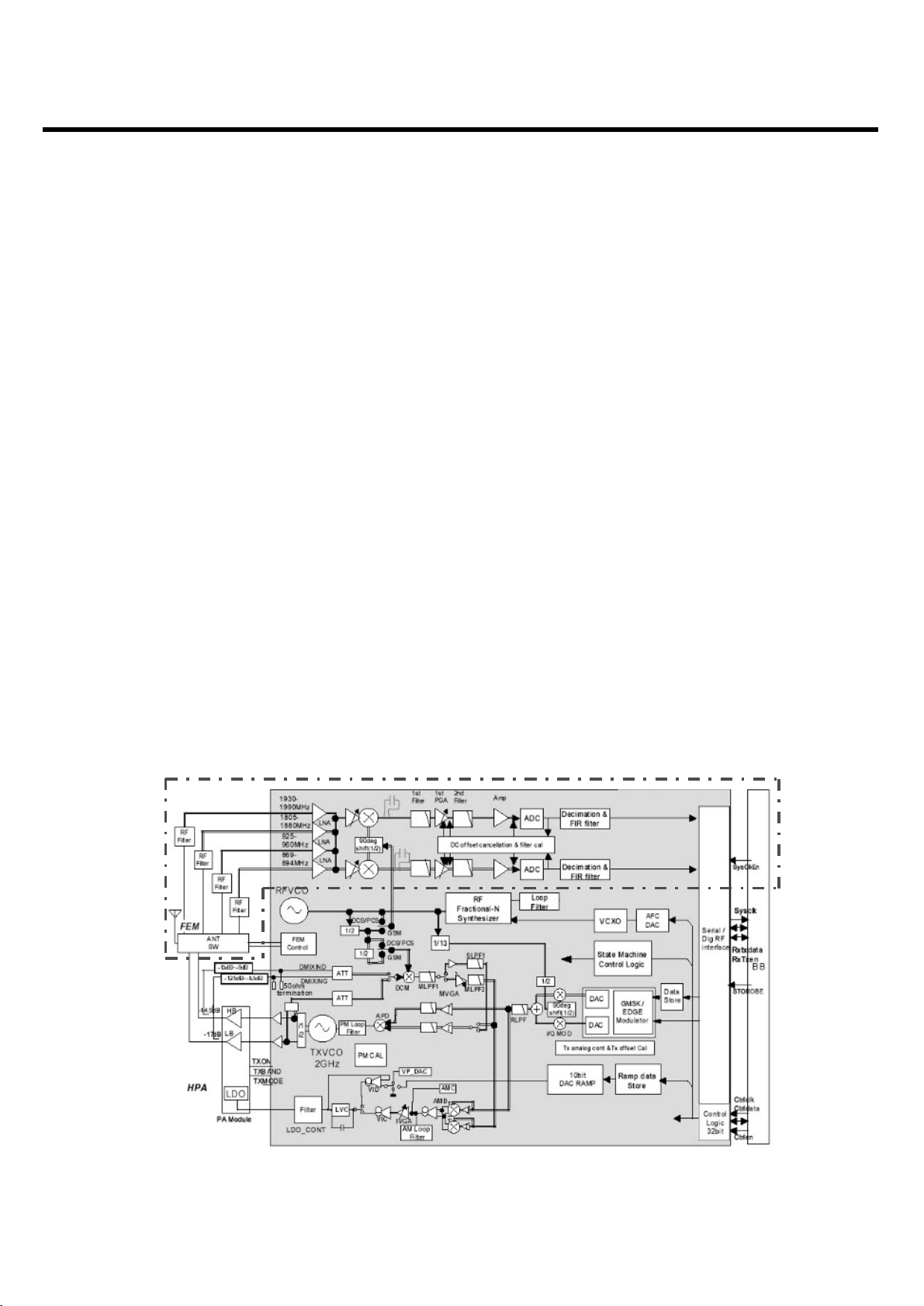
The RF part consists of a transmitter, a receiver, a synthesizer, a voltage supply and a DCXO part.
The main RF Chipset B6PLD is a highly integrated RF tranceiver IC FOR Digital Interface of GSM 850,
GSM900, DCS1800 and PCS1900 quad-band cellualr systems. The B6PLD incorporates EDGE
tranceiver apability, quad R low-noise amplifiers(LNSa). Direct conversion mixers, a programmable
gain amplifier(PGA) with DC offset and frequency response correction, ADC, Digital filiter, Digital
Interface, fully integrated VCOs, an RF fractiona-N synthesiser, a low-noise offset PLL transmitter,
Digital modulator, TXDAC, RAMPDAC, and AFCDAC. The B6PLD includes state machine control
through serial programming. All functions operate down to 2.67V and are housed in a 72-pin BGA
package. Hence the B6PLD can form a small size transceiver handset for quad band EDGE
tranceiver.
3.2 RF Part
3.2.1 Receiver Part
The B6PLD receiver supports quad band, so the front-end incorporates four LNAs and two mixers.
The incoming RF signals are mixed directly down to I/Q baseband by the front-end bolck. This
incorporates four LNAs/four buffers and two Gillbert Cell mixer blocks optimised for operation at
850MHz, 900MHz, 1800MHz and 1900MHz respectively. The front-end block is followed by two
closely matched baseband amplifier chains. These include distributed low pass filtering, one switched
gain stage and one fixed gain stage. In addition, the baseband section integrates A/D and D/A
converters which provide automatic on-chip correction of DC offsets.
<Fig.1> Receiver Part Block Diagram

LGE Internal Use Only
Copyright © 2007 LG Electronics. Inc. All right reserved.
Only for training and service purposes
3.2.1.1 Baseband PGA/Low pass Filter Specifications
The baseband programmable amplifier comprises one stage with variable gain followed by a fixed
gain amplifier. The overall gain control range is 36dB with 6dB Steps. The filtering is provided by a
single R/C low pass filter with an on-chip capacitor followed by on-chip Chebychev low pass filters.
The filters have been specified to achieve maximal group delay flatness in the pass-band combined
with the required levels of suppression of interfering signals. The distribution of the gain and filtering
has been designed to ensure that the receiver does not compress under blocking conditions. The
final fixed gain amplifier is included to match the on-chip levels to the input dynamic range of the
ADC.
3.2.1.2 DC offset auto-calibration system
B6PLD implements a system for cancelling the DC offsets in the baseband programmable gain
amplifiers(PGA). This prevents a small DC offset at the input giving a large DC offset at the output,
even at high gain settings. When the B6PLD receiver is performing an auto-calibration, the
sequencer cancels the offsets locally around the PGA, then the Digital filter. The system includes
switches to short out the signal path whilst the cancellation is occurring. The switches are opened in
sequence as the calibration progresses. For PGA the A/D converter system employs a successive
approximation technique and achieves 6 bit resolution. The PGA stage has an associated 6 bit
current DAC which cancels the DC offset at the output. The sequencer ensures that on-chip filters
have sufficient time to settle before applying correction in the next digital offset cancellation stage.
3. Circuit Description
- 18 -
LGE Internal Use Only
Copyright © 2007 LG Electronics. Inc. All right reserved.
Only for training and service purposes
3. Circuit Description
- 19 -
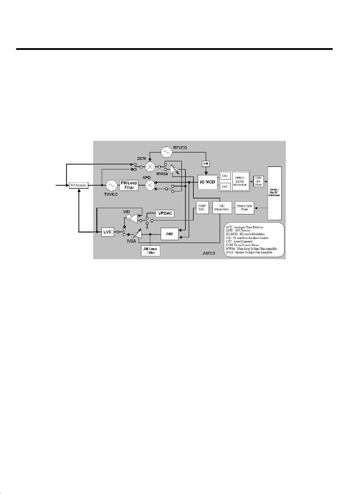
3.2.2 Transmitter part
The B6PLD transmitter is capable of both GMSK and 8-PSK modulation, to support for conventional
GSM and EDGE. B6PLD integrates all loop filters to configure both PM loop and AM loop. See block
diagram below.
3.2.2.1 Polar Loop Structure
Three main functions are identified in the transmitter architecture; I/Q vector modulation at IF
frequency, amplitude and phase loop at IF/RF frequencies and power amplification.
Fig. Simplified Block diagram for Tx part

LGE Internal Use Only
Copyright © 2007 LG Electronics. Inc. All right reserved.
Only for training and service purposes
3.2.3 RF Systhesiser
3.2.4 Front End Module Specification
3.2.4.1 Block Diagram and Internal Matching Condition
3. Circuit Description
- 20 -
LMSP43MA
LGE Internal Use Only
Copyright © 2007 LG Electronics. Inc. All right reserved.
Only for training and service purposes
3. Circuit Description
- 21 -
3.2.4.2 Logic Table for Selction
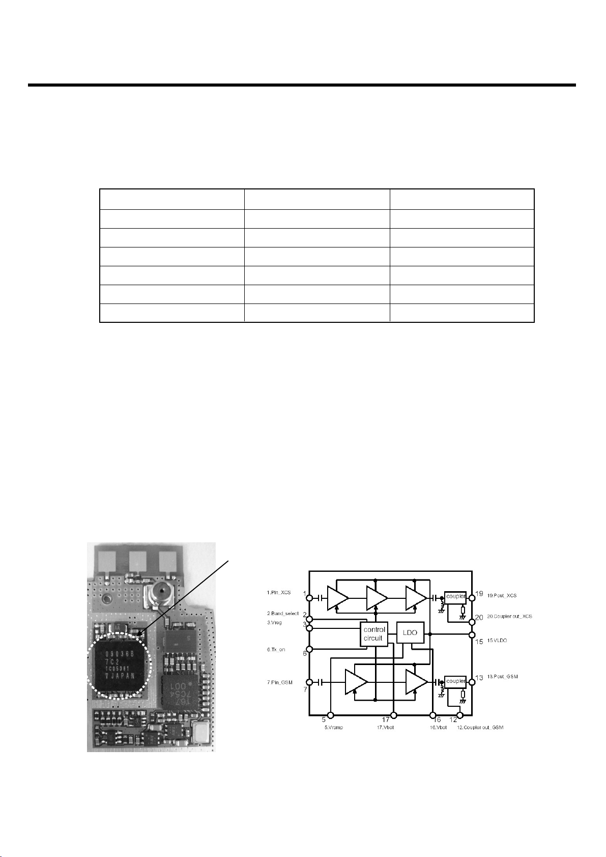
3.2.5 Power Amplifier Module
for Quad-band GSM/GPRS/EDGE
3.2.5.1 PAM Specification
-. Quad band GSM, GPRS & Ploar Loop EDGE Amplifier
-. For 3.5V nominal operation
-. Bulit-in LDO circuit
-. GPRS Class 12 operation compatible
-. Integrated directional coupler
3.2.5.2 Circuit Diagram and peripheral components
Select Mode Vc1(GSM850) Vc(DCS/PCS)
GSM850_Rx Low Low
EGSM_Rx Low Low
GSM850_Tx High Low
DCS_Rx Low Low
PCS_Rx Low Low
DCS/PCS_Tx Low High
<Table 1.> Band SW Logic Table
RPF09036B
LGE Internal Use Only
Copyright © 2007 LG Electronics. Inc. All right reserved.
Only for training and service purposes
3.2.6 Digital Core
3.2.6.1 Digital Interface Block Diagram
3. Circuit Description
- 22 -
Fig. 1-1 Digital Interface Block Digram

LGE Internal Use Only
Copyright © 2007 LG Electronics. Inc. All right reserved.
Only for training and service purposes
3. Circuit Description
- 23 -
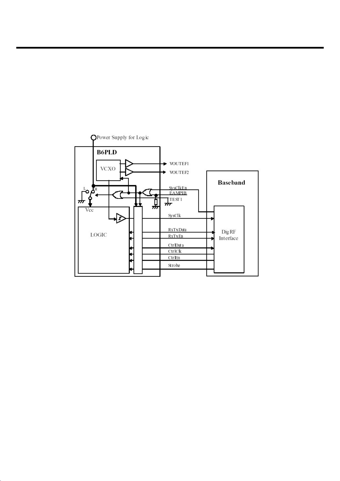
3.2.6.2 Control system and digital interface
The B6PLD is a RF transceiver IC for GSM850, DCS1800 and PCS1900 Tri band cellular system,
and incorporates EDGE transceiver capability. The B6PLD has a digital interface connection to the
baseband processor. This interface complies with the digital interface specification DigRF standard
v112. The digital interface consists of two separate interface connections; (1) the control interface, (2)
the data interface, and a system clock on/off control signal and a precise timing singal. These are
realized by eight signal lines in B6PLD(Look at Fig1.1 above)
- The control interfce is used to configure the B6PLD for RX and TX operation, transfers of control
data for several built-in circuits, and for triggering the events. The control interface comprise a bidirectional 3-wire serial interface with the three signal lines CtrlData, CtrlEn and CtrlClk accessing
the control registers in B6PLD by transferring the control words.
-. The data interface is used to transfer transmit modulation symbols and receive IQ-sampling data.
The data interface comprises a single serial bus with the three signal lines RxTxData, RxTxEn and
SysClk. The SysClk is used for system clock to baseband.
-. The SsClkEn signal enables the SysClk output and powers the 26MHz oscillator on. When the
SysClkEn is negated, the SysClk is held low, and if the TEST1 pin is low by the default settings, the
logic power supply by typical 1.8 volts to the internal core logic circuits is also switched off.
LGE Internal Use Only
Copyright © 2007 LG Electronics. Inc. All right reserved.
Only for training and service purposes
3.3 Digital Baseband
3.3.1 General description
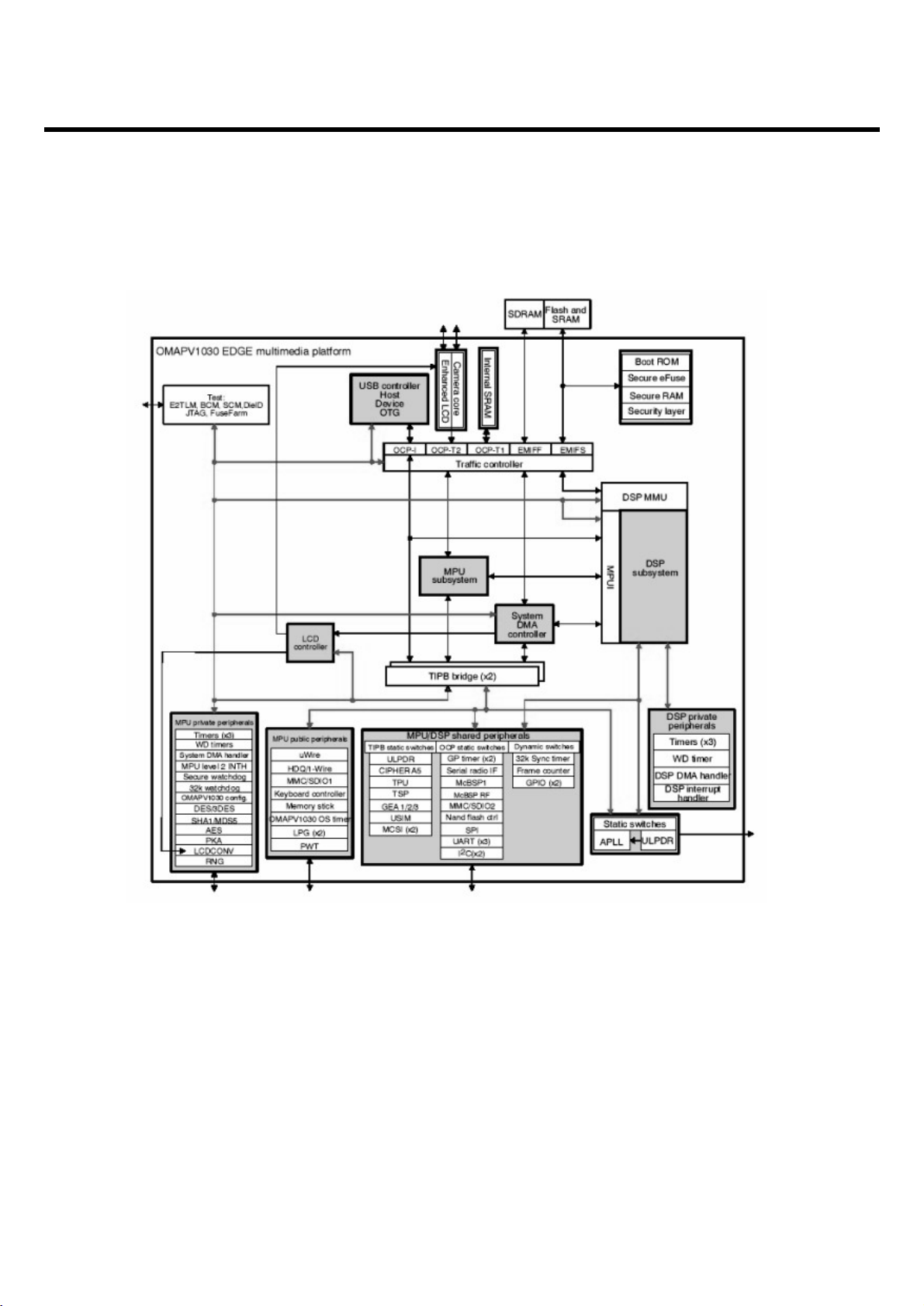
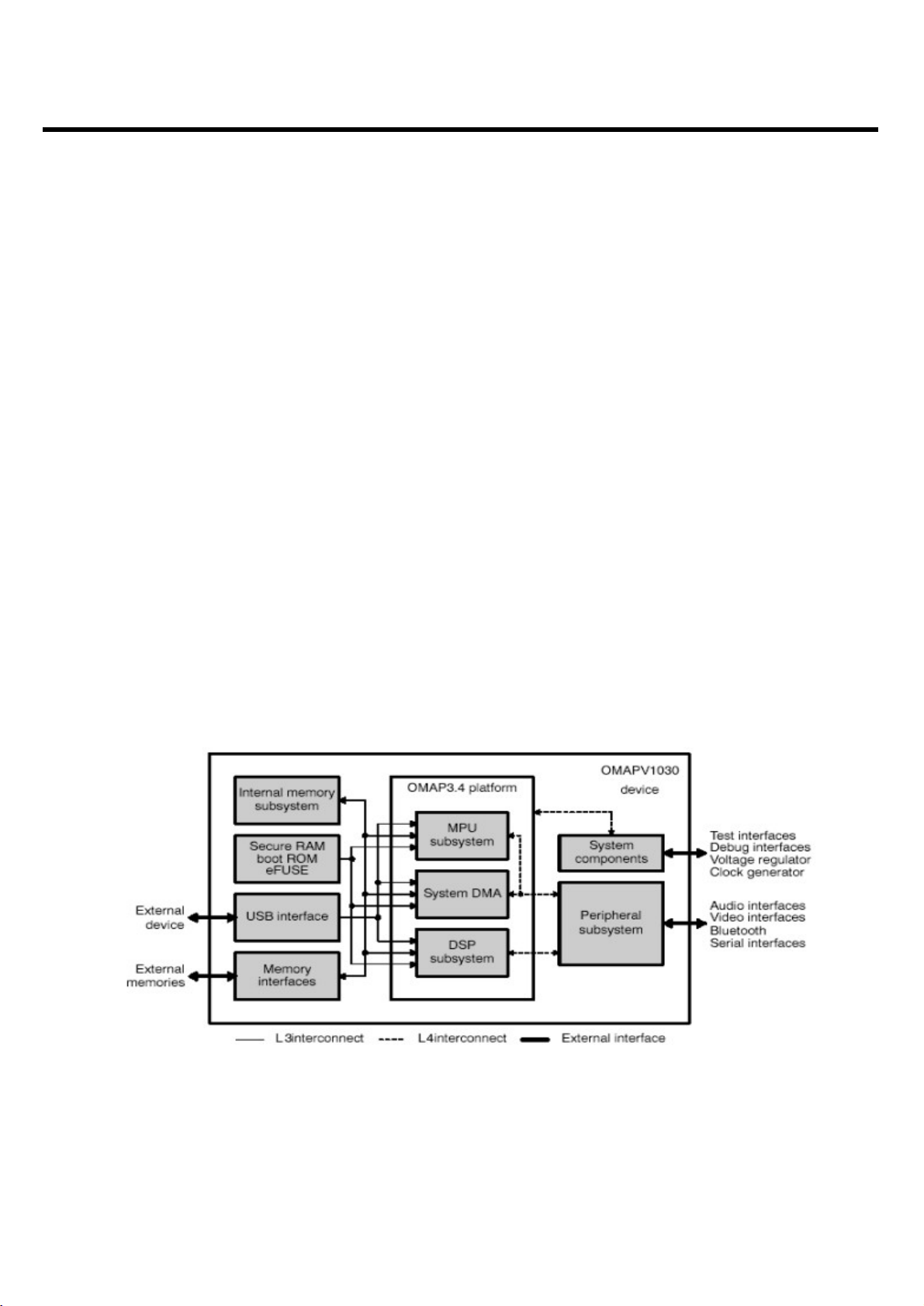
The OMAPV1030 E-GPRS multimedia device belongs to the Texas Instruments OMAP-Vox_
processors family. It combines both a modem engine and an application engine. Memory and CPU
resources are shared between modem and application processing. The OMAPV1030 chip is based
on the OMAP3.4 architecture and integrates two processor subsystems:
- An MPU subsystem based on an ARM926EJ-S
- A DSP subsystem based on a UMA 2.6 architecture integrating a C55x DSP core The
OMAPV1030’s silicon process technology is a c027.0 90-nm digital CMOS.
3. Circuit Description
- 24 -
<Fig.6> OMAPV1030 Block Diagram
LGE Internal Use Only
Copyright © 2007 LG Electronics. Inc. All right reserved.
Only for training and service purposes
3.3.2 Block Description
The OMAPV1030 E-GPRS multimedia device is based on an OMAP3.4 platform that integrates:
- The MPU subsystem
- The DSP subsystem
- A system DMA
- A traffic controller providing:
- External memory interfaces with:
- A slow interface (EMIFS) to ROM, SRAM, FLASH memories
- A fast interface (EMIFF) to SDRAM memories
- Layer 3 (L3) interconnect made of two OCP target ports (OCP-T1 and OCP-T2) and one OCP
initiator port (OCP-I)
- Layer 4 (L4) interconnect made of two DSP peripheral busses (private DSP TIPB and shared DSP
TIPB) and two MPU peripheral busses (public MPU TIPB and private MPU TIPB)
- Clock management
- A set of processor peripherals:
- Three 32-bit timers, a 16-bit Watchdog timer, and an interrupt handler for the MPU
- Three 32-bit timers, a 16-bit Watchdog timer, and a 2nd-level interrupt handler for the DSP
- Test and debug interfaces (JTAG, Window Tracer)
- Trace capabilities: ETM9 and Ctools
The other OMAPV1030 modules or subsystems are connected to the OMAP3.4 platform through the
L3 and L4 interconnects.
3. Circuit Description
- 25 -
<Fig.7> OMAPV1030 Top-Level Architecture Overview

LGE Internal Use Only
Copyright © 2007 LG Electronics. Inc. All right reserved.
Only for training and service purposes
The OMAP3.4 platform is the computing core of the device. The other OMAPV1030 components are
organized as follows:
- The internal memory subsystem is made of a single-port 256K-bit shared internal SRAM.
- The security subsystem is a set of several components, including dedicated a secure mode to run
secure applications.
- A master-slave USB module provides an external interface supporting high data transfer rates
between the OMAPV1030 and external application
- The memory interfaces provide access to external memories. There are two types of memory
controllers:
- SDRAM controller supporting SDR and DDR modes
- General-purpose controller supporting asynchronous and synchronous
- The system components are used to manage system interactions such as interrupts, clock control,
reset control, and idle management.
- The peripheral subsystem refers to all the peripherals accessible by the MPU and/or the DSP. They
are all OCP- or TIPB-compliant and are connected to the OMAP3.4 platform through the traffic
controller or the TIPB busses.
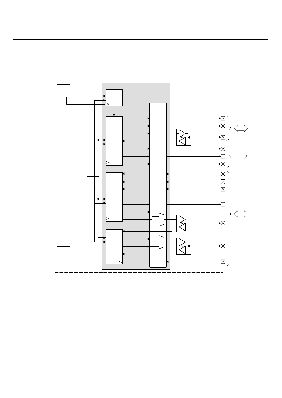
3.3.3 RF Interface (Digital RF Interface)
The OMAPV1030 radio interface module of OMAPV1030 device is an interface that carries the
following information:
- Transmit symbols from DBB to RF IC
- Receive samples from RF IC to DBB
- Bidirectional information control
- Real-time and activation signals from DBB to RF IC
- System clock
The OMAPV1030 radio interface module of OMAPV1030 device supports two types of radio
interfaces. They differ mainly in the type of data interface:
- The first interface is based on a standard six-wire scheme: three wires for transmit and three for
receive.
- The second one is based on a two-wire bidirectional scheme: one wire for data in/out, and one for
control receive/transmit.
3. Circuit Description
- 26 -
LGE Internal Use Only
Copyright © 2007 LG Electronics. Inc. All right reserved.
Only for training and service purposes
This implementation is based on the following:
- The time processing unit (TPU) module is a real-time sequencer dedicated to monitoring GSM
baseband processing.
- The serial port of the time serial port (TSP) module controls both interfaces.
- The real-time TSPACT signal of the TSP module
- The McBSP digital RF module is used for the six-wire data interface.
- The serial radio interface module is used for the two-wire data interface.
- A system clock interface receives a squared 26-MHz clock from the RF IC.
3. Circuit Description
- 27 -
<Fig.8> OMAPV1030 Radio Interface
ULPDR
GSM_clock_13M
GSM_clock_26M
MPU public
CLKM1
TIPB
DSP
shared
TIPB
ARMPER_CK
OMAPV1030 Radio I/F
TPU
TPU BUS
TSP
McBSP
digital
RF
Serial
Radio
IF
PODIGRFDO
PIDIGRFDI
TSPCLK
TSPEN
TSPDO
TSPDI
TSPACT3
TSPACT4
TSPACT5
CLKR
DR
FSR
CLKX
DX
FSX
PIRXEN
POTXEN
PICLKM
I/O
CORE
MUX
OMAPV1030 device
digitalrf_rf_clk
digitalrf_rf_cs
digitalrf_rf_data
digitalrf_tx_start
digitalrf_enr
digitalrf_rxen
digitalrf_rx_clk
digitalrf_rx_data
digitalrf_rx_cs
digitalrf_tx_clk
digitalrf_tx_cs /
digitalrf_enable
digitalrf_tx_data /
digitalrf_data
digitalrf_sysclk
RF CTRL IF
RF real-
time IF
RF DATA IF
LGE Internal Use Only
Copyright © 2007 LG Electronics. Inc. All right reserved.
Only for training and service purposes
3. Circuit Description
- 28 -
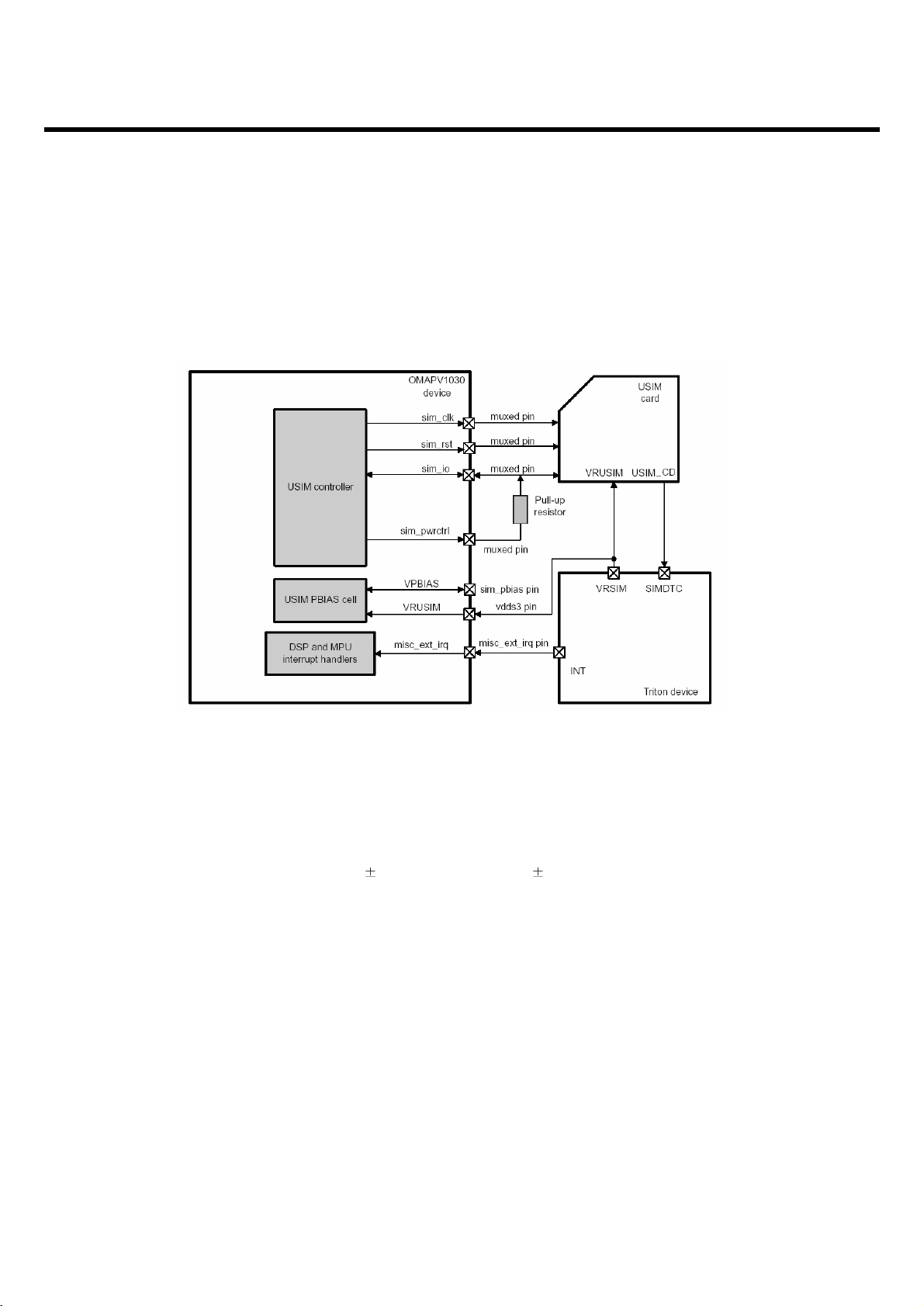
3.3.4 SIM interface
SIM interface scheme is shown in below.
SIM_IO, SIM_CLK, SIM_RST, SIM_PWRCTRL ports are used to communicate DBB via ABB with
plugged sim card and the LDO (VRSIM) in ABB enables operate 1.8V to 2.5V to search SIM card
SIM_CLK : SIM Card reference clock SIM_PWCTRL : SIM Card power activation
SIM_RST : SIM Card async/sync reset SIM_IO : SIM Card bi-directional data line
VRUSIM(Power supply VCC) : 3 V 10% (class B) or 1.8 V 10% (class C)
Misc_ext_irq : USIM card presence detection (USIM_CD) purposes.
<Fig.9> SIM Interface
LGE Internal Use Only
Copyright © 2007 LG Electronics. Inc. All right reserved.
Only for training and service purposes
3. Circuit Description
- 29 -
3.3.5 UART Interface
CE110 has Three UART Drivers as follow :
- UART1 : USB - UART2 : ETM, Calibration - UART3 : AT command, Fax_modem, Bluetooth
UART1(USB)
Resource Name Description
USB_DP DP Data
USB_DM DM Data
USB_PWR POWER USB_POWER
VBUS VBUS USB_Detect
UART2 (ETM)
DEBUG_RX RX Receive Data(UART2)
DEBUG_TX TX Transmit Data(UART2)
UART3 (Bluetooth)
UART3_RXD UART3_RXD Receive Data
UART3_TXD UART3_TXD Transmit Data
UART3_RTS UART3_RTS Request To Send
UART3_CTS UART3_CTS Clear To Send
<Table.2> UART Interface Spec
- 30 -
3. Circuit Description
3.3.6 GPIO Map
In total 22 allowable resources, CE110 is using 16 resources except 3 resources dedicated to SIM
and Memory. CE110 GPIO(General Purpose Input/Output) Map, describing application, I/O state,
and enable level, is shown in below table 3.
LGE Internal Use Only
Copyright © 2007 LG Electronics. Inc. All right reserved.
Only for training and service purposes
I/O # Net Name I/O
Resource Inactive Active
State State State
I/O (1) LCD_SUB_CS HIGH LOW
I/O (2) CAM_PWON I Sysboot LOW HIGH
I/O (4) USB_BOOT_SEL I Sysboot LOW (Giant Plus) HIGH (Nanya)
I/O (6) Pull Up I Sysboot HIGH LOW
I/O (8) BT_NRST O GPIO LOW (LCD B/L Off) HIGH (LCD B/L On)
I/O (9) CHG_EN O GPIO LOW HIGH
I/O (12) CAM_RST O GPIO HIGH LOW
I/O (13) UART_RST I GPIO HIGH LOW
I/O (16) UART_CST I Sysboot LOW HIGH
I/O (17) BOOT_SEL I GPIO HIGH HIGH
I/O(19) CAM_PWR_EN I GPIO LOW HiIGH
I/O(32) SPK_EN O GPIO HIGH LOW
I/O (42) VCAM18_EN I GPIO LOW HIGH
I/O(43) CHG_STAT O GPIO HIGH LOW
I/O (46) KEY_BL_EN I GPIO LOW HIGH
I/O (47) LCD_BL_EN O GPIO LOW HIGH
<Table.3> GPIO Map
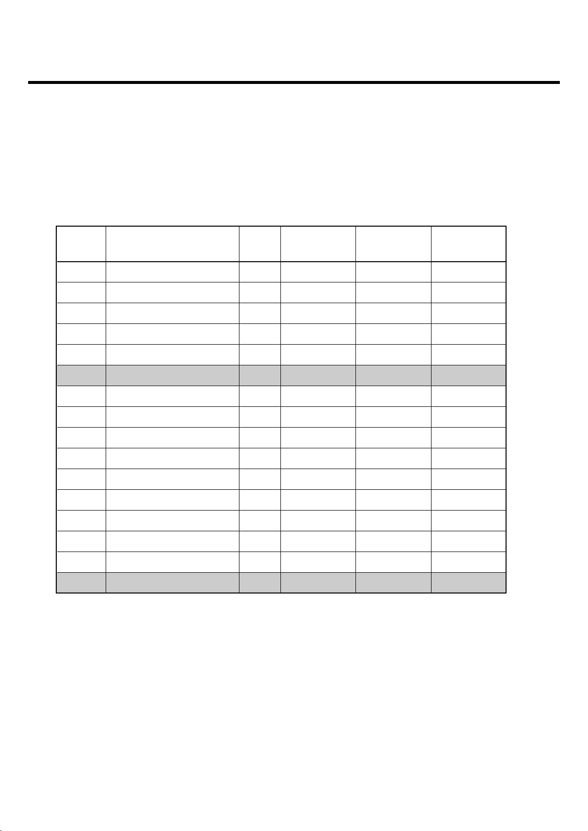
- 31 -
3. Circuit Description
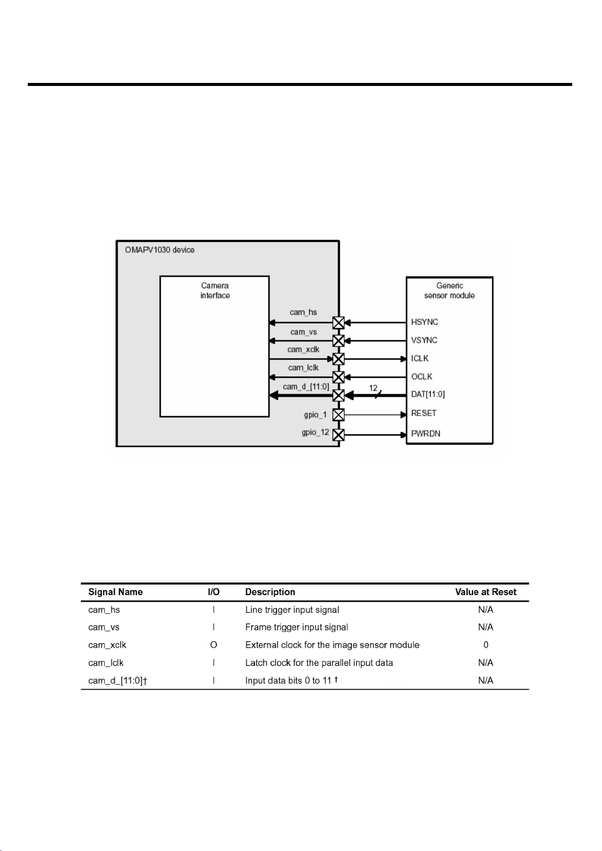
3.3.7 Camera interface
CE110 have a 8-bit parallel camera interface(NOBT Mode). This is a general parallel interface with
vertical and horizontal synchronization signals.(See. Figure 12) The maximum clock is 96 MHz for 8bit data data, or 48 MHz for 10- or 12-bit data.
Table7. describes the I/O signals of the generic parallel camera interface.
Figure13, Figure14 show the frame and data timing according to synchronization signals in the
parallel NOBT configuration.
LGE Internal Use Only
Copyright © 2007 LG Electronics. Inc. All right reserved.
Only for training and service purposes
<Fig.10> Generic Parallel Camera Interface
<Table 4> Generic Parallel Camera Interface
 Loading...