

Page 1
PIONEER CORPORATION 4-1, Meguro 1-chome, Meguro-ku, Tokyo 153-8654, Japan
PIONEER ELECTRONICS (USA) INC. P.O. Box 1760, Long Beach, CA 90801-1760, U.S.A.
PIONEER EUROPE NV Haven 1087, Keetberglaan 1, 9120 Melsele, Belgium
PIONEER ELECTRONICS ASIACENTRE PTE. LTD. 253 Alexandra Road, #04-01, Singapore 159936
PIONEER CORPORATION 2006
ORDER NO.
RROVISIONAL
CDJ-800MK2
COMPACT DISC PLAYER
CDJ-800MK2
THIS MANUAL IS APPLICABLE TO THE FOLLOWING MODEL(S) AND TYPE(S).
Model Type Power Requirement Remarks
CDJ-800MK2 KUCXJ AC120V
CDJ-800MK2 WYXJ5 AC220-240V
CDJ-800MK2 RLFXJ AC110-120V / 220-240V
For details, refer to "Important symbols for good services" .
T-ZZR APR. 2005 printed in Japan
Page 2
-
1234
SAFETY INFORMATION
A
This service manual is intended for qualified service technicians ; it is not meant for the casual do-it
yourselfer. Qualified technicians have the necessary test equipment and tools, and have been trained
to properly and safely repair complex products such as those covered by this manual.
Improperly performed repairs can adversely affect the safety and reliability of the product and may
void the warranty. If you are not qualified to perform the repair of this product properly and safely, you
should not risk trying to do so and refer the repair to a qualified service technician.
WARNING
This product contains lead in solder and certain electrical parts contain chemicals which are known to the state of California to
causecancer, birth defects or other reproductive harm.
B
NOTICE
(FOR CANADIAN MODEL ONLY)
Fuse symbols (fast operating fuse) and/or (slow operating fuse) on PCB indicate that replacement
parts must be of identical designation.
REMARQUE
(POUR MODÈLE CANADIEN SEULEMENT)
Les symboles de fusible (fusible de type rapide) et/ou (fusible de type lent) sur CCI indiquent que
les pièces de remplacement doivent avoir la même désignation.
Health & Safety Code Section 25249.6 – Proposition 65
C
(FOR USA MODEL ONLY)
1. SAFETY PRECAUTIONS
The following check should be performed for the
continued protection of the customer and
service technician.
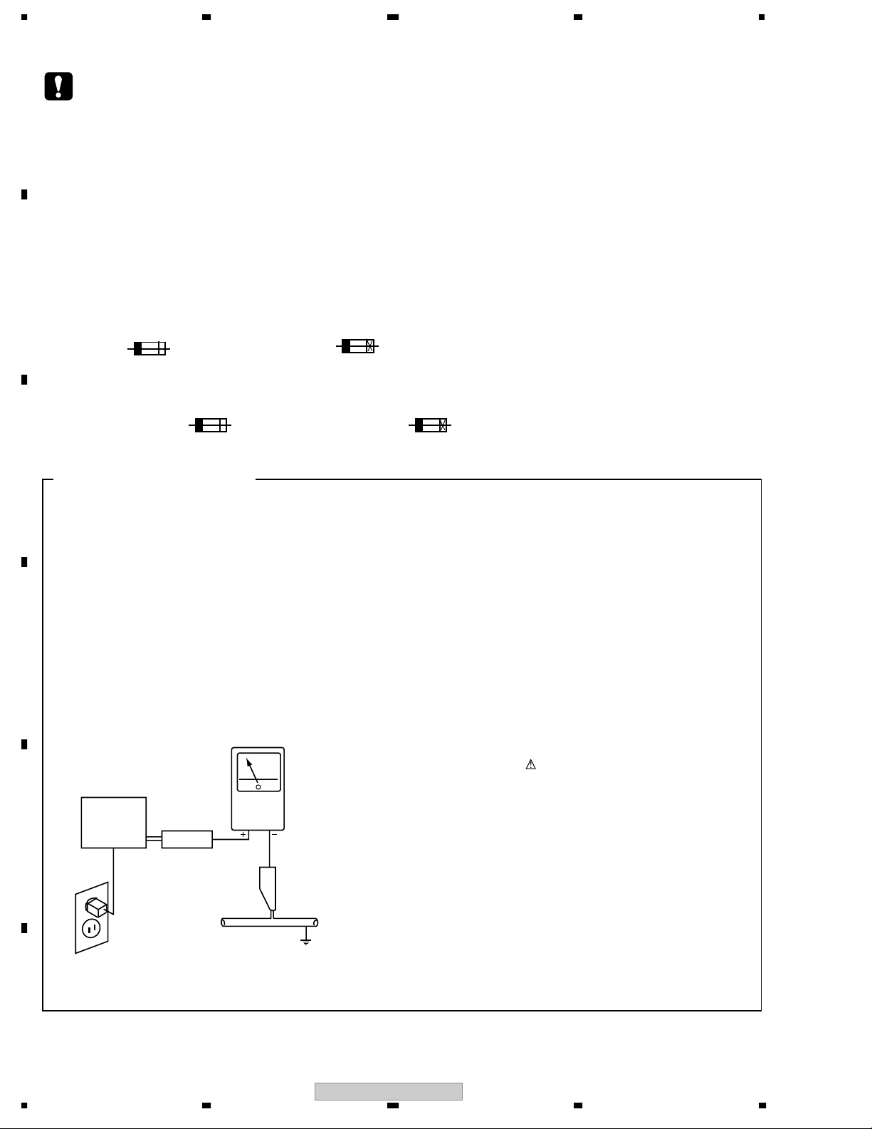
LEAKAGE CURRENT CHECK
Measure leakage current to a known earth ground (waterpipe
, conduit, etc.) by connecting a leakage current tester
such as Simpson Model 229-2 or equivalent between the
D
earth ground and all exposed metal parts of the appliance
(input/output terminals, screwheads, metal overlays, control
shaft, etc.). Plug the AC line cord of the appliance directly
into a 120V AC 60Hz outlet and turn the AC power switch
on. Any current measured must not exceed 0.5mA.
Reading should
Leakage
Device
under
E
test
Also test with
plug reversed
(Using AC adapter
plug as required)
Test all
exposed metal
surfaces
current
tester
not be above
0.5mA
Earth
ground
ANY MEASUREMENTS NOT WITHIN THE LIMITS
OUTLINED ABOVE ARE INDICATIVE OF A POTENTIAL
SHOCK HAZARD AND MUST BE CORRECTED BEFORE
RETURNING THE APPLIANCE TO THE CUSTOMER.
2. PRODUCT SAFETY NOTICE
Many electrical and mechanical parts in the appliance
have special safety related characteristics. These are
often not evident from visual inspection nor the protection
afforded by them necessarily can be obtained by using
replacement components rated for voltage, wattage, etc.
Replacement parts which have these special safety
characteristics are identified in this Service Manual.
Electrical components having such features are identified
by marking with a on the schematics and on the parts list
in this Service Manual.
The use of a substitute replacement component which does
not have the same safety characteristics as the PIONEER
recommended replacement one, shown in the parts list in
this Service Manual, may create shock, fire, or other hazards.
Product Safety is continuously under review and new
instructions are issued from time to time. For the latest
information, always consult the current PIONEER Service
Manual. A subscription to, or additional copies of, PIONEER
Service Manual may be obtained at a nominal charge
from PIONEER.
AC Leakage Test
F
2
1234
CDJ-800MK2
Page 3
5678
THIS PIONEER APPARATUS CONTAINS
IMPORTANT
LASER OF CLASS 1.
SERVICING OPERATION OF THE APPARATUS
SHOULD BE DONE BY A SPECIALLY
INSTRUCTED PERSON.
The AEL(accessible emission level) of the laser power output is less then CLASS 1
but the laser component is capable of emitting radiation exceeding the limit for
CLASS 1.
A specially instructed person should servicing operation of the apparatus.
LABEL CHECK
MAXIMUM OUTPUT POWER: 5 mW
WAVELENGTH: 780 – 785 nm
WARNING !
CDJ-800MK2 WYXJ5 and KUCXJ : Types Only
LASER DIODE CHARACTERISTICS
for RLFXJ
(DRW2308)
A
B
C
Bottom Plate
Printed on the Bottom Plate
(DRW2408)
Additional Laser Caution
1. Laser Interlock Mechanism
The position of the switch (S2401) for detecting loading
completion is detected by the system microprocessor, and
the design prevents laser diode oscillation when the switch
is not in LPS1 terminal side (when the mechanism is not
clamped and LPS1 signal is high level.) Thus, the interlock
will no longer function if the switch is deliberately set to LPS1
terminal side. ( if LPS1 signal is low level ).
In the test mode
Laser diode oscillation will continue, if pin 5 of AN22022A
(IC601)on the MAIN ASSY is connected to GND,
or pin 10 of IC118 (LDON) is connected to low level
(ON), or else the terminals of Q603 are shorted to each
other (fault condition).
2. When the cover is opened, close viewing of the objective
lens with the naked eye will cause exposure to a Class 1
laser beam.
∗ the interlock mechanism will not function.
∗ : Refer to page 53.
D
E
56
CDJ-800MK2
F
3
7
8
Page 4
1234
[Important Check Points for Good Servicing]
In this manual, procedures that must be performed during repairs are marked with the below symbol.
Please be sure to confirm and follow these procedures.
1. Product safety
A
Please conform to product regulations (such as safety and radiation regulations), and maintain a safe servicing environment by
following the safety instructions described in this manual.
1 Use specified parts for repair.
Use genuine parts. Be sure to use important parts for safety.
2 Do not perform modifications without proper instructions.
Please follow the specified safety methods when modification(addition/change of parts) is required due to interferences such as
radio/TV interference and foreign noise.
B
C
D
3 Make sure the soldering of repaired locations is properly performed.
When you solder while repairing, please be sure that there are no cold solder and other debris.
Soldering should be finished with the proper quantity. (Refer to the example)
4 Make sure the screws are tightly fastened.
Please be sure that all screws are fastened, and that there are no loose screws.
5 Make sure each connectors are correctly inserted.
Please be sure that all connectors are inserted, and that there are no imperfect insertion.
6 Make sure the wiring cables are set to their original state.
Please replace the wiring and cables to the original state after repairs.
In addition, be sure that there are no pinched wires, etc.
7 Make sure screws and soldering scraps do not remain inside the product.
Please check that neither solder debris nor screws remain inside the product.
8 There should be no semi-broken wires, scratches, melting, etc. on the coating of the power cord.
Damaged power cords may lead to fire accidents, so please be sure that there are no damages.
If you find a damaged power cord, please exchange it with a suitable one.
9 There should be no spark traces or similar marks on the power plug.
When spark traces or similar marks are found on the power supply plug, please check the connection and advise on secure
connections and suitable usage. Please exchange the power cord if necessary.
0 Safe environment should be secured during servicing.
When you perform repairs, please pay attention to static electricity, furniture, household articles, etc. in order to prevent injuries.
Please pay attention to your surroundings and repair safely.
2. Adjustments
To keep the original performance of the products, optimum adjustments and confirmation of characteristics within specification.
Adjustments should be performed in accordance with the procedures/instructions described in this manual.
3. Lubricants, Glues, and Replacement parts
Use grease and adhesives that are equal to the specified substance.
Make sure the proper amount is applied.
E
4. Cleaning
For parts that require cleaning, such as optical pickups, tape deck heads, lenses and mirrors used in projection monitors, proper
cleaning should be performed to restore their performances.
5. Shipping mode and Shipping screws
To protect products from damages or failures during transit, the shipping mode should be set or the shipping screws should be
installed before shipment. Please be sure to follow this method especially if it is specified in this manual.
F
4
1234
CDJ-800MK2
Page 5

5678
CONTENTS
SAFETY INFORMATION......................................................................................................................................2
1. SPECIFICATIONS.............................................................................................................................................6
2. EXPLODED VIEWS AND PARTS LIST.............................................................................................................8
2.1 PACKING ....................................................................................................................................................8
2.2 EXTERIOR SECTION ..............................................................................................................................10
2.3 CONTROL PANEL SECTION...................................................................................................................12
2.4 SLOT-IN MECHANISM SECTION ............................................................................................................14
3. BLOCK DIAGRAM AND SCHEMATIC DIAGRAM ..........................................................................................16
3.1 BLOCK DIAGRAM....................................................................................................................................16
3.2 BLOCK DIAGRAM (2) ..............................................................................................................................18
3.3 BLOCK DIAGRAM (Power).......................................................................................................................20
3.4 OVERALL WIRING DIAGRAM .................................................................................................................22
3.5 MAIN (1/3) and RLYB ASSYS ..................................................................................................................24
3.6 MAIN ASSY(2/3).......................................................................................................................................26
3.7 MAIN ASSY(3/3).......................................................................................................................................30
3.8 AC IN, TRNS, SECB and REGB ASSYS..................................................................................................32
3.9 DFLB, JACK and KSWB ASSYS..............................................................................................................34
3.10 JFLB, SLDB, SLMB and JOGB ASSYS .................................................................................................36
3.11 WAVEFORMS.........................................................................................................................................38
3.12 VOLTAGES..............................................................................................................................................42
4. PCB CONNECTION DIAGRAM ......................................................................................................................47
4.1 MAIN ASSY ..............................................................................................................................................48
4.2 RLYB ASSY ..............................................................................................................................................52
4.3 SECB ASSY .............................................................................................................................................54
4.4 TRNS ASSY..............................................................................................................................................58
4.5 AC IN ASSYS ...........................................................................................................................................60
4.6 DFLB ASSY..............................................................................................................................................62
4.7 REGB and JACK ASSYS..........................................................................................................................66
4.8 KSWB ASSY.............................................................................................................................................68
4.9 JFLB ASSY...............................................................................................................................................70
4.10 SLDB ASSY............................................................................................................................................74
4.11 SLMB and JOGB ASSYS .......................................................................................................................76
5. PCB PARTS LIST............................................................................................................................................78
6. ADJUSTMENT ................................................................................................................................................83
7. GENERAL INFORMATION .............................................................................................................................84
7.1 DIAGNOSIS..............................................................................................................................................84
7.1.1 SERVICE MODE................................................................................................................................84
7.1.2 RESET and CLOCK MAP ..................................................................................................................90
7.1.3 TROBLE SHOOTING .........................................................................................................................92
7.1.4 POWER ON SEQUENCE ..................................................................................................................98
7.1.5 DISASSEMBLY ..................................................................................................................................99
7.2 PARTS ....................................................................................................................................................107
7.2.1 IC......................................................................................................................................................107
7.2.2 DISPLAY ..........................................................................................................................................115
8. PANEL FACILITIES .......................................................................................................................................116
A
B
C
D
56
CDJ-800MK2
E
F
5
7
8
Page 6
1234
1. SPECIFICATIONS
Specifications
A
• KUCXJ type
1. General
System..............................Compact disc digital audio system
Power requirements.....................................AC 120 V, 60 Hz
Power consumption.......................................................20 W
Operating temperature.......... +5˚C to +35˚C (+41˚F to +95˚F)
Operating humidity...............................................5 % to 85 %
(There should be no condensation of moisture.)
Weight..............................................................4.0 kg (8.8 lb)
Dimensions..................... 305 (W) × 344.1 (D) × 106.5 (H)mm
B
12 (W) × 13 –9/16 (D) × 4 – 1/4 (H) in
• RLFXJ type
1. General
System........................... Compact disc digital audio system
Power requirements .... AC 110-120 V/220-240 V, 50/60 Hz
Power consumption ..................................................... 22 W
For Taiwan: 21 W
Operating temperature ..................................+5°C to +35°C
Operating humidity ........................................... 5 % to 85 %
(There should be no condensation of moisture.)
Weight ........................................................................4.0 kg
Dimensions .................. 305 (W) x 344.1 (D) x 106.5 (H) m
m
2. Audio section
Frequency response........................................4 Hz to 20 kHz
Signal-to-noise ratio..........................115 dB or more (JEITA)
Distortion.................................................... .0.006 % (JEITA)
3. Accessories
• Operating instructions........................................................1
• Power cord........................................................................1
• Audio cable....................................................................... 1
• Control cable..................................................................... 1
C
• Forced eject pin (housed in a groove in the bottom panel)... 1
• Limited warranty................................................................1
NOTE:
Specifications and design are subject to possible modification
with-out notice.
• WYXJ5 type
1. General
System.......................... Compact disc digital audio system
Power requirements .................... AC 220-240 V, 50/60 Hz
D
Power consumption ..................................................... 22 W
Operating temperature .................................. +5°C to +35°C
Operating humidity ............................................ 5 % to 85 %
(There should be no condensation of moisture.)
Weight ....................................................................... 4.0 kg
Dimensions ..................305 (W) x 344.1 (D) x 106.5 (H) mm
2. Audio section
Frequency response...................................... 4 Hz to 20 kHz
Signal-to-noise ratio ....................... 115 dB or more (JEITA)
Distortion ................................................... 0.006 % (JEITA)
3. Accessories
• Operating instructions ..................................................... 1
• Power cord ...................................................................... 1
• Audio cable ..................................................................... 1
• Control cable ................................................................... 1
• Forced eject pin (housed in a groove in the bottom panel)... 1
NOTE:
Specifications and design are subject to possible modification
with-out notice.
Voltage selector (RLFXJ type only)
• You can find the voltage selector switch on the bottom plate
of the unit.
The factory setting for the voltage selector is 220 – 240 V.
Please set it to the correct voltage for your country or region.
• For Taiwan, please set to 110 – 120 V before using.
Before changing the voltage, disconnect the AC power cord.
Use a medium size screwdriver to change the voltage
selector switch.
220-240V
2. Audio section
Frequency response...................................... 4 Hz to 20 kHz
Signal-to-noise ratio ....................... 115 dB or more (JEITA)
Distortion ................................................... 0.006 % (JEITA)
E
3. Accessories
• Operating instructions ..................................................... 1
• Power cord ...................................................................... 1
• Audio cable ..................................................................... 1
• Control cable ................................................................... 1
• Forced eject pin (housed in a groove in the bottom panel)... 1
NOTE:
Specifications and design are subject to possible modification
with-out notice.
F
6
1234
110-120V
CDJ-800MK2
Page 7
5678
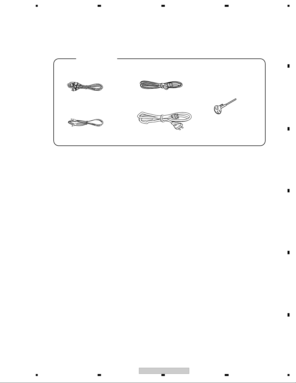
A
Accessories
Audio Cable
(VDE1064) L=1.5m
Control Cord
(XDE3063) L=1 m
Power Cord
(ADG7021 : KUCXJ)
(ADG1154 : WYXJ,RLFXJ)
Forced Fject Pin
(housed in a groove in
the bottom panel)
(DEX1008)
B
C
D
E
F
56
CDJ-800MK2
7
7
8
Page 8
1234
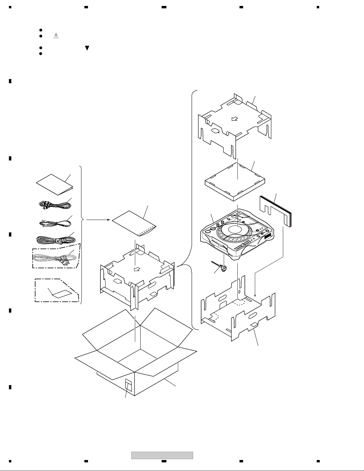
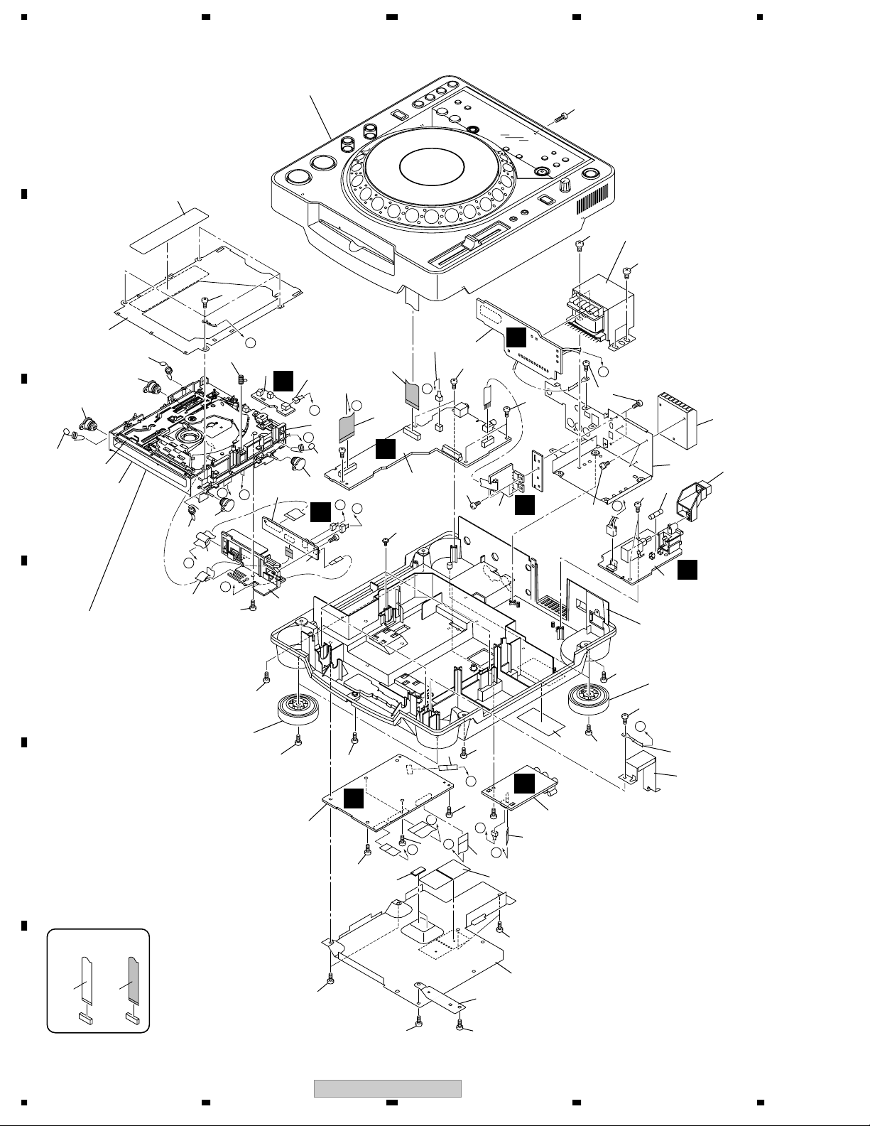
2. EXPLODED VIEWS AND PARTS LIST
NOTES:
A
Parts marked by "NSP" are generally unavailable because they are not in our Master Spare Parts List.
The mark found on some component parts indicates the importance of the safety factor of the part.
Therefore, when replacing, be sure to use parts of identical designation.
Screws adjacent to mark on product are used for disassembly.
For the applying amount of lubricants or glue, follow the instructions in this manual.
(In the case of no amount instructions, apply as you think it appropriate.)
2.1 PACKING
B
C
6
7
4
8
3
5
2
9
1
1
D
E
RLFXJ type only
13
KUCXJ type
only
10
11
12
14
F
8
1234
CDJ-800MK2
Page 9
>
>
>
5678
PACKING parts List
No. Description Part No.
No. Description Part No.
Mark
1 AC Power Cord See Contrast table(2)
2 Control Cord XDE3063
3 Audio Cord VDE1064
4 Operating Instructions See Contrast table(2)
5 Polyethylene Bag AHG7117
6 Pad B DHA1556
7 Pad C DHA1557
8 Pad D DHA1558
Mark
9 Sheet RHX1006
10 Push Rod DEX1008
11 Pad A DHA1555
12 Packing Case See Contrast table(2)
NSP 13 Warranty Card See Contrast table(2)
NSP 14 Label DRW2311
(2) CONTRAST TABLE
CDJ-800MK2/KUCXJ, /WYXJ5 and RLFXJ types are constructed the same except for the following:
Mark No. Symbol and Description
1 AC Power Cord ADG7021 ADG1154 ADG1154
1 AC Power Cord Not used Not used ADG7O97
4 Operating Instructions (English)(KUCXJ) DRB1401 Not used Not used
4 Operating Instructions (WYXJ5)(English, Not used DRB1400 Not used
French, German, Italian, Dutch, Spanish)
CDJ-800MK2/
KUCXJ
CDJ-800MK2/
WYXJ5
CDJ-800MK2/
RLFXJ
A
B
4 Operating Instructions (RLFXJ) Not used Not used DRB1402
(English, Spanish, Chinese)
12 Packing Case DHG2595 DHG2594 DHG2596
NSP 13 Warranty Card ARY7043 Not used Not used
C
D
E
56
CDJ-800MK2
F
9
7
8
Page 10
1234
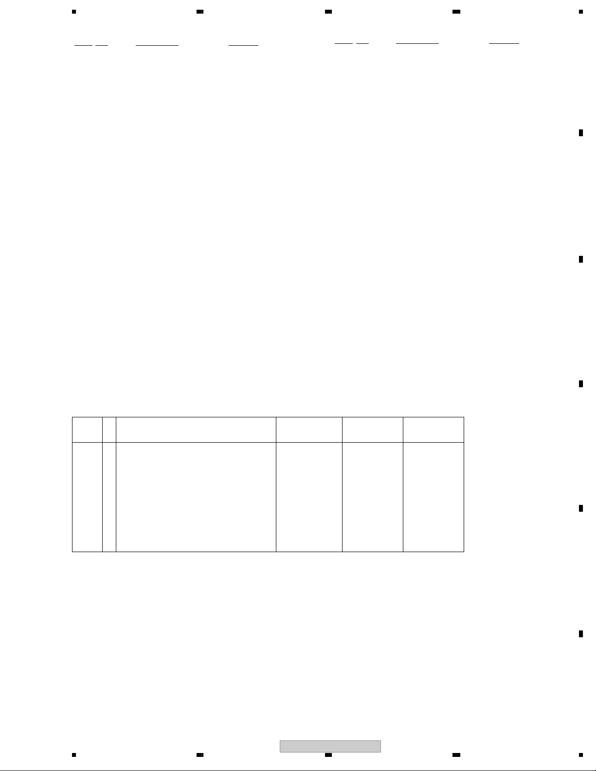
2.2 EXTERIOR SECTION
Refer to
"2.3 CONTROL PANEL SECTION".
A
38
42
43
17
43
B
35
33
31
31x4
33x4
C
D
E
34
20
Refer to
"2.4 SLOT-IN MECHANISM SECTION".
33
G
15
31
12
F
44
A
32
6
18
M
B
37
D
33
31
9-(b)
E
B
7
E
44
36
44
30
46x4
14
C
13
C
B
D
44
A
1
44
22
45
19
44
H
4
F
44
41
11
44
C
G
D
3
I
39
41
46
41
24
28
10
44
I
E
2
29
44
30
44
A
16
25
21
44
F
5
44
J
H
12
I
8
11
J
23
F
10
NON-CONTACT
CONTACT SIDE
SIDE
1234
44
44
CDJ-800MK2
40
26
27
44
Page 11
>
>
>
>
>
>
>
>
>
5678
EXTERIOR SECTION parts List
No. Description Part No.
Mark
1 MAIN Assy DWG1622
2 AC IN Assy See Contrast table(2)
3 TRNS Assy See Contrast table(2)
4 SECB Assy DWR1309
5 REGB Assy DWR1310
6 SLMB Assy DWS1388
7 RLYB Assy DWX2602
8 JACK Assy DWG1626
9• • • •
10 Fuse See Contrast table(2)
11 FFC (9p) DDD1311
12 FFC (32p) DDD1312
13 FFC (25p) DDD1313
14 FFC (17p) DDD1314
15 FFC (24p) DDD1315
NSP 16 Earth Lead DE010VF0
17 Power Transfomer See Contrast table(2)
18 Connector Assy PF03PP-B05
19 Connector Assy PF03PP-C12
NSP 20 SLOTINMECHA SV Assy DXA2005
21 Power Knob DAC2073
NSP 22 Silicon Lubber D5 L DEB1456
23 Bottom Cushion S4 DEC2506
24 Heat Sink DNG1102
No. Description Part No.
Mark
25 Earth Plate DNH2532
26 Bottom Plate See Contrast table(2)
27 Bottom Earth Plate DNH2694
28 Trans Plate DNH2733
NSP 29 Chassis See Contrast table(2)
30 Insulator Assembly DXA2069
31 Damper CNV6011
32 Earth Spring DBH1398
33 Float Spring (G5) DBH1494
34 Front Sheet DED1132
35 Mecha Plate DNH2642
36 PCB Holder DNK4524
37 Float Base 04 Assy DXB1838
38 Laser Caution (7L) DRW2308
NSP 39 Serial Label (UPC) See Contrast table(2)
40 Screw BBT30P060FCC
41 Screw BBZ30P060FTC
42 Screw BBZ30P100FTC
43 Screw BBZ40P060FTC
44 Screw BPZ30P080FTB
45 DM Screw (FTC) DBA1260
46 Screw IPZ30P100FTC
A
B
C
(2) CONTRAST TABLE
CDJ-800MK2/KUCXJ, /WYXJ5 and RLFXJ types are constructed the same except for the following:
Mark No. Symbol and Description
2 AC IN ASSY DWR1430 DWR1429 DWR1432
3 TRANS ASSY DWR1371 DWR1371 DWR1428
10 Fuse (T1.6A) AEK7075 Not used Not used
10 Fuse (800MA) Not used REK1021 REK1021
17 Power Transfomer DTT1204 DTT1203 DTT1203
26 Bottom Plate DNK2689 DNK2689 DNK2691
29 Chassis DNK4518 DNK4517 DNK4519
NSP 39 Serial Label DRW2311 VRW1629 VRW1629
CDJ-800MK2/
KUCXJ
CDJ-800MK2/
WYXJ5
CDJ-800MK2/
RLFXJ
D
E
56
CDJ-800MK2
F
11
7
8
Page 12
1234
2.3 CONTROL PANEL SECTION
8
A
B
C
D
E
Grease: GYA1001( ZLB-PN397B)
1
*
C
38-(b)
38-(c)
37
58
50
2
H
58
58
58
49
B
48-1
58
45
46
B
58
47
21
51
9
52
31
53
41
5656x3
17
A
40
43
23
14
33
G
*
38-(a)
58
1
*
10
17
1
1
*
C
56
22
1
*
58
54x2
5
D
6
35
42
34
36
6
58
D
J
4
58
58
39
39
44
48-2
58
32
A
1
58
12
57
L
13
*
13
10
10x3
13
13
E
*
58
1
1
*
15
16
3
K
26
28
18x9
17x3
13x12
27
58
29
1
1
*
30x8
20
1
*
58
25
24
11
19
F
12
NON-CONTACT
CONTACT SIDE
SIDE
1234
CDJ-800MK2
7
58
E
58
55
Page 13

5678
CONTROL PANEL SECTION parts List
No. Description Part No.
Mark
1 DFLB Assy DWG1623
2 KSWB Assy DWS1386
3 JFLB Assy DWG1624
4 SLDB Assy DWS1387
5 JOGB Assy DWG1625
6 FFC DDD1220
7 Connector Assy PF04PP-B07
8 Jog Panel (PMMA) DAH2182
9 Jog Plate DAH2438
10 SW spring 25 DBH1514
No. Description Part No.
Mark
50 FFC Guard DEC2586
51 Reloop Guard DNK4057
52 Q R Guard DNK4058
53 Control Panel DNK4525
54 Screw BPZ20P060FTC
55 Screw BPZ20P100FTC
56 Screw (FE) DBA1265
57 Screw IPZ30P100FTC
58 Screw BPZ30P080FTB
A
11 Gear spring 200 DBH1525
12 ARM Sprimg DBH1566
13 SW Cushion HH48/2 DEC2538
14 Encorder Plate DEC2889
15 Protector Sheet DEC2945
16 FL Sheet DEC2946
17 Ring Cushion L24/2.0 DEC2958
18 SW Ring DNK4070
19 Adjust Plate DNK4178
20 Jog Holder DNK4545
21 Jog B DNK4557
22 Gear ARM DNK4559
23 Gear DNK4560
24 Smoother DNK4561
25 Load Gear A DNK4562
26 Jog A DNK4586
27 Sheet SW DSX1065
28 Roller A Assy DXB1825
29 Jog Stay Assy DXB1876
30 Roller B Assy DXB1877
B
C
D
31 Rotary Knob C DAA1194
32 TEMPO Knob DAC2061
33 VINYL Knob DAC2063
34 LOOP Knob DAC2066
35 Auto Beat Loop Knob DAC2069
36 Quick Return Knob DAC2070
37 PLAY Knob DAC2286
38 Set Knob (Eject) DAC2287
39 CALL Knob DAC2289
40 RELOOP Knob DAC2291
41 Slide Knob DAC2292
42 TEXT/A.CUE Knob DAC2294
43 Folder Search Knob DAC2298
44 DEL/MEMO Knob DAC2299
45 Reverse Knob DAC2364
46 Slide Sheet (gray) DAH2374
47 Display Panel DAH2418
48 Earth Plate (CU) DBK1224
49 Vessel Sheet DEC2495
56
CDJ-800MK2
E
F
13
7
8
Page 14
1234
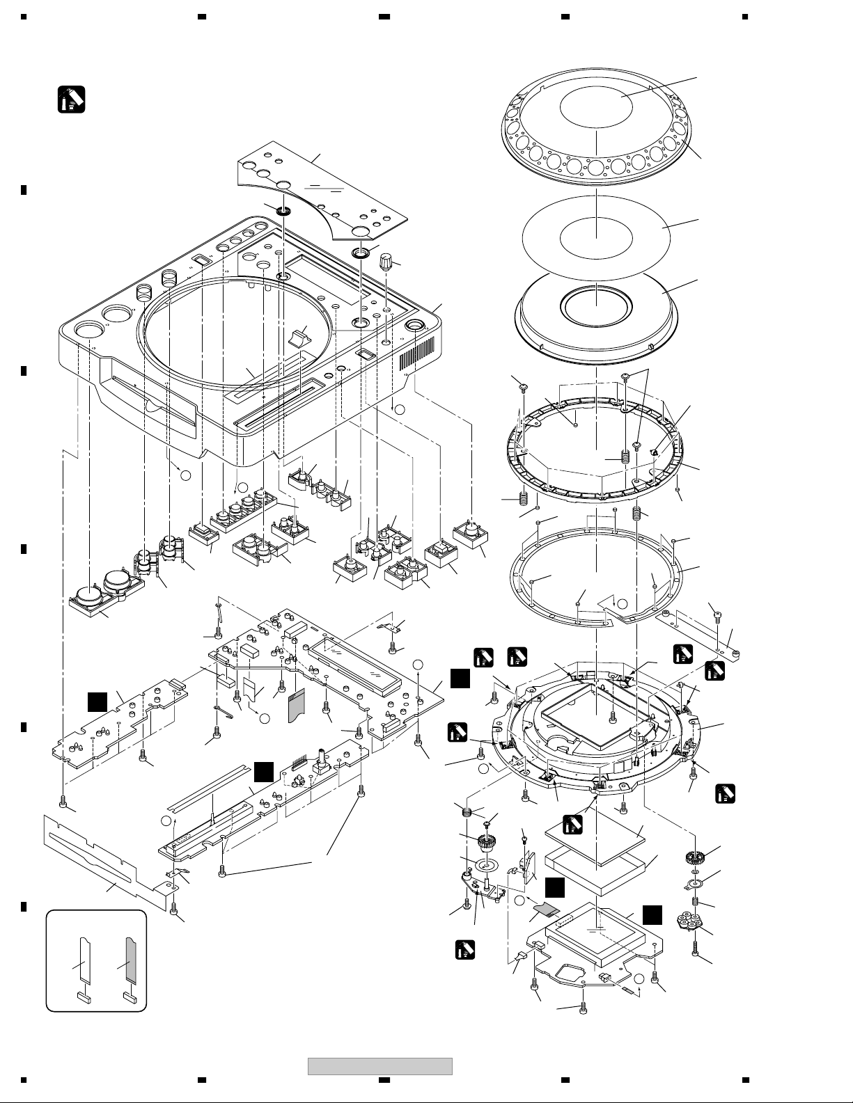
2.4 SLOT-IN MECHANISM SECTION
Grease
A
GYA1001
1
(ZLB-PN397B)
11
20
21
Dyefree
23
B
7
10
GEM1036
(ZLX-ME413A)
9
Grease
GYA1001
(ZLB-PN397B)
13
19
C
8
Dyefree
GEM1036
15
(ZLX-ME413A)
16
Dyefree
GEM1036 (ZLX-ME413A)
25
Cleaning liquid : GEM1004
Cleaning paper : GED-008
RLYB CN12
To
(Pickup)
12
18
17
22
24
14
3
4
5
To
RLYB CN16
(Loading Motor)
D
25
(Stepping Motor)
To
RLYB CN14
25
Grease
GYA1001
(ZLB-PN397B)
6
27
31
25
2
Note:
The TM. Assy 03-S is supplied only in
assembly form, not as a single part.
E
30
29
F
28
30
26
To MAIN CN102
(Spindle Motor)
NON-CONTACT
SIDE
CONTACT SIDE
14
CDJ-800MK2
1234
Page 15

5678
SLOT-IN MECHANISM SECTION parts List
No. Description Part No.
Mark
NSP 1 Slot-in Mecha SV Assy DXA2005
2 TM. Assy 03-S VXX3125
3 DC Motor Assy-S DXX2510
NSP 4 Worm Gear DNK3910
NSP 5 DC Motor S (ROHS) DXM1230
6 Connector Assy PF02PY-B22
7 Clamp Spring DBH1374
8 Guide Spring DBH1375
9 SW Lever Spacer SV DEC2831
10 Loading Lever DNK3406
A
11 Main Cam DNK3407
12 Disc Guide DNK3478
13 Clamp Arm DNK3576
14 Eject Lever DNK3684
15 Lever AP DNK3835
16 Lever BP DNK3836
17 Loading Gear DNK3911
18 Drive Gear DNK3912
19 Loading Base SV DNK4369
20 SW Lever SV1 DNK4370
21 SW Lever SV2 DNK4371
22 Gear Holder SV DNK4372
23 Clamper 04 Assy DXB1859
24 Screw BPZ20P060FTC
25 Floating Rubber (SI) VEB1351
26 Float Base 04 Assy DXB1838
27 Spacer POR (T3) DEB1566
28 Vessel Cushion A DEC2852
29 Vessel Cushion B DEC2853
30 Vessel Cushion C DEC2854
31 Front Sheet DED1132
B
C
D
56
CDJ-800MK2
E
F
15
7
8
Page 16
1234
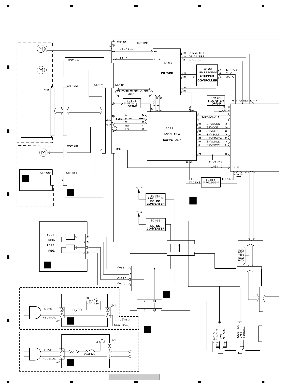
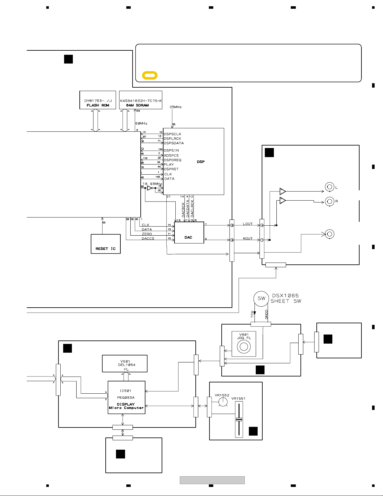
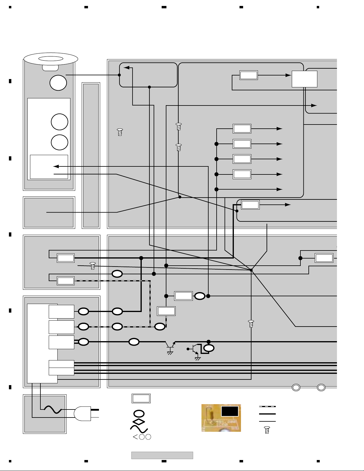
3. BLOCK DIAGRAM AND SCHEMATIC DIAGRAM
3.1 BLOCK DIAGRAM
A
TM. ASSY 03-S (VXX3125)
SPINDLE
MOTOR 04
B
C
Loading MOTOR
ASSY-S
(DXM1230)
STEPPING
MOTOR 04
PICKUP ASSY
M
SLMB ASSY
SLOT-IN
MECHANISM SV
ASSY
RLYB ASSY
B
M63018FP
COMPARATOR
MAIN ASSY
A
D
J91
BA008C0WCP
BA008C0WCP
REGB ASSY
F
E
F
For KUCXJ, WYXJ5
For RLFXJ
ACIN ASSY
E
ACIN ASSY
E
S2
S1
BROWN
VIOLET
BLUE
CN52
V+3D
CN51
CN22
J2
J3
NJM2885DL1
CN301
CN53
TRNS ASSY
D
SECB ASSY
C
CN301
CN53
CN56
CN50
16
CDJ-800MK2
1234
Page 17
5678
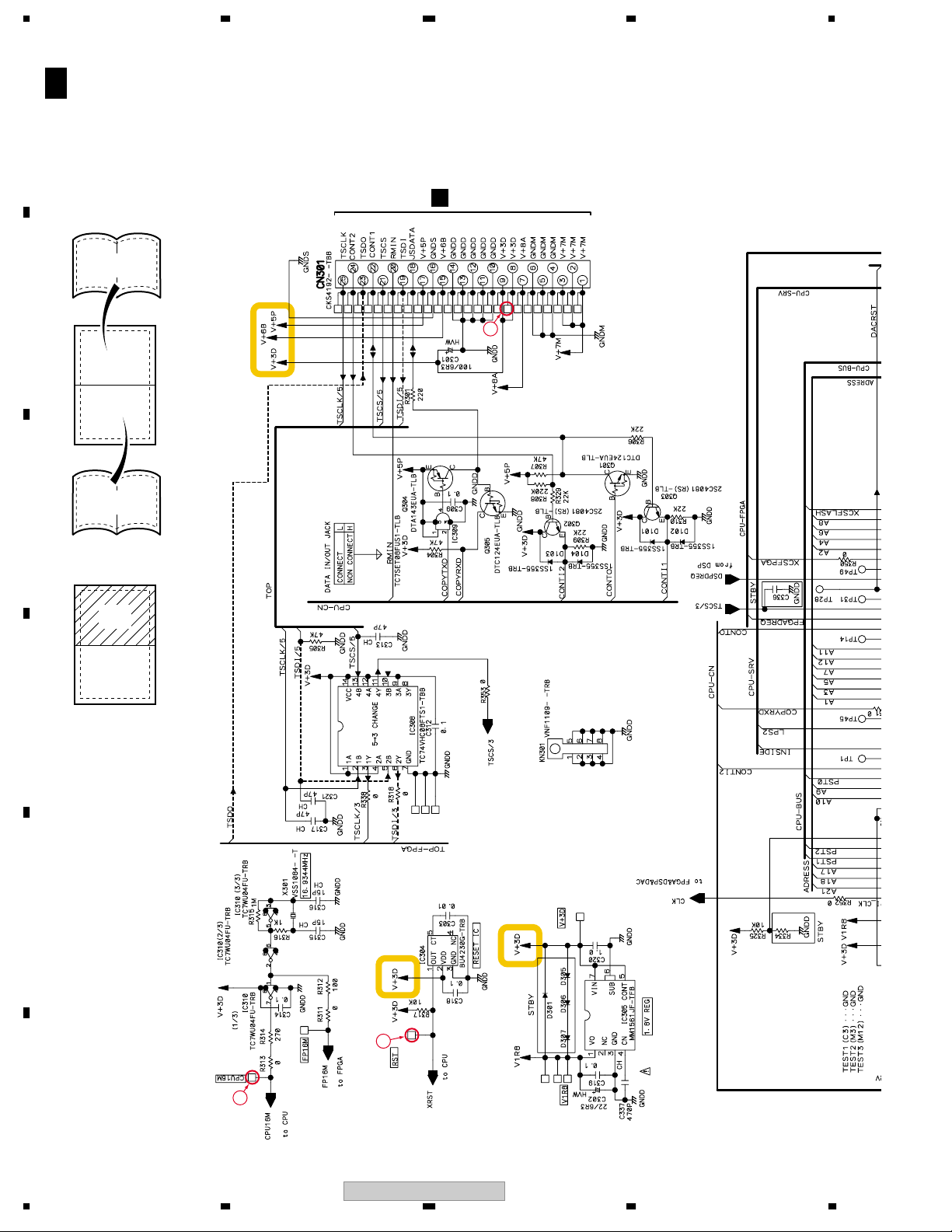
MAIN ASSY
A
IC300
IC301
SCF5249VM140-K
MPU
IC304
BU4230G
÷
When ordering service parts, be sure to refer to "EXPLODED VIEWS and PARTS LIST" or
"PCB PARTS LIST".
÷
The > mark found on some component parts indicates the importance of the safety factor
of the part. Therefore, when replacing, be sure to use parts of identical designation.
÷
IC303
: The power supply is shown with the marked box.
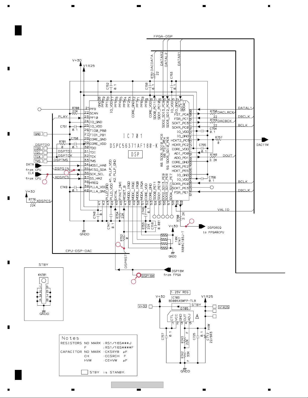
IC701
DSPC56371AF180-K
IC702
PE8001A
CN701
CN801
I
JACK ASSY
IC801
OP AMP
JA801
DKB1053
JA802
PKB1033
DIGITAL OUT
A
B
AUDIO OUT
C
DFLB ASSY
G
CN501
CN502
CN500
CN503
CN600
CN1503
CN602
CN601
K
JFLB ASSY
SLDB ASSY
J
CN802
D
CN1601
L
JOGB ASSY
E
CN1502
H
KSWB ASSY
CDJ-800MK2
56
F
17
7
8
Page 18
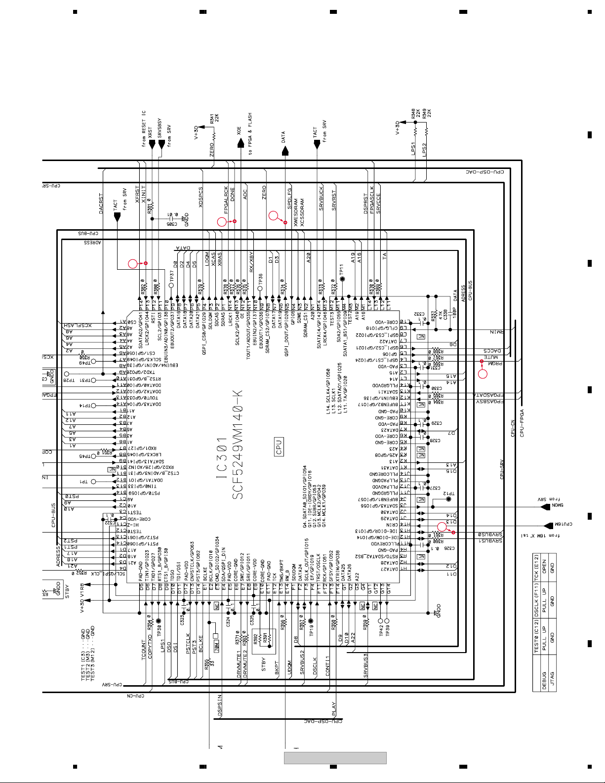
1234
R
S
R
C
C
R
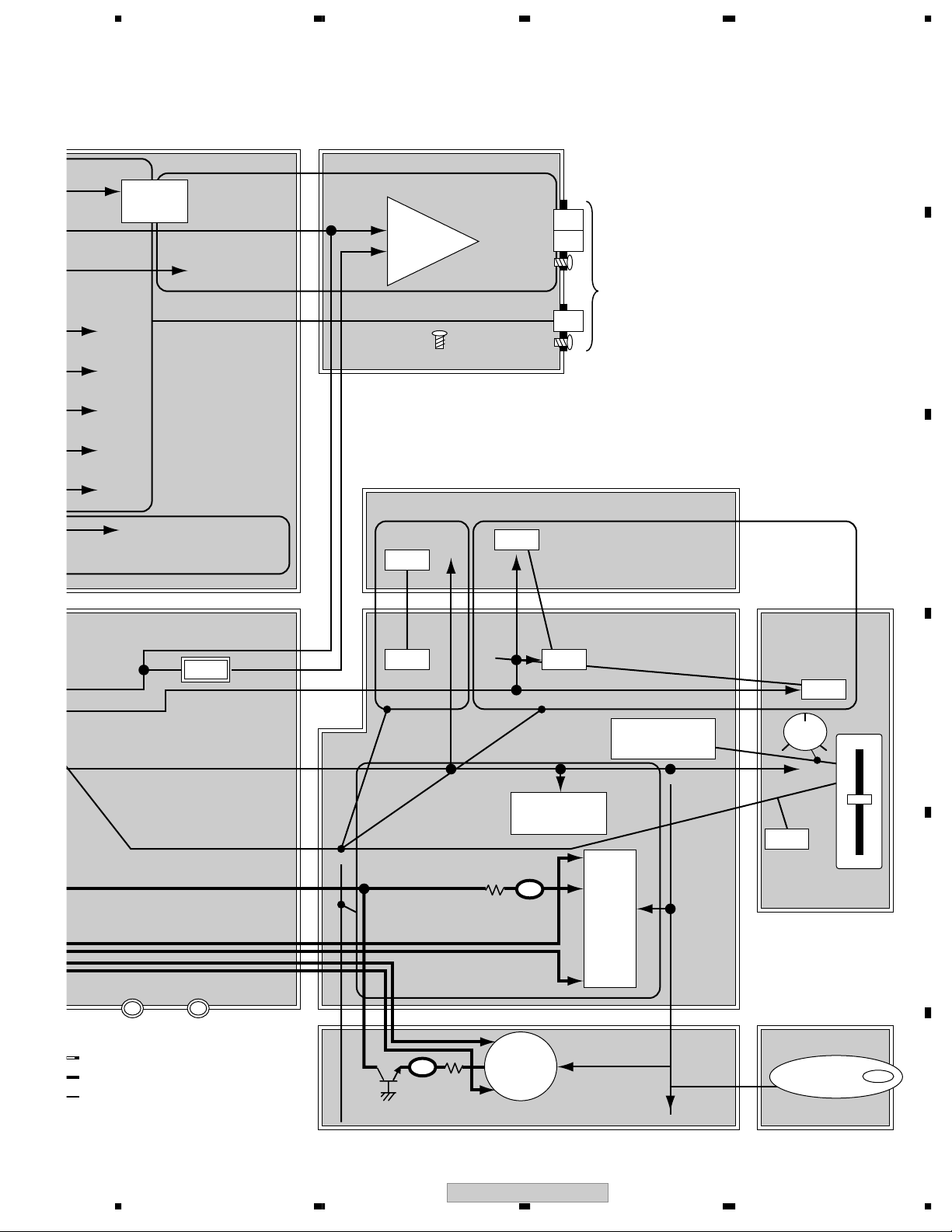
3.2 BLOCK DIAGRAM (2)
• Blick diagra Map
A
CD DRIVE BLOCK
AUDIO BLOCK
MAIN ASSY
Loading
TRAVERS
B
SLED
Spindle
MECHA
M
M
M
KP 2PIN
IC101
SERVO DSP
DWX2602-A/J
KP 4PINFFC17PINKP 3PIN
IC102 DRIVER
DWG1622-A/J
IC701
AUDIO
DSP
I
Pickup ASSY
IC302
FPGA
(50000GATE)
DRIVE ASSY
C
SLMB ASSY
DWS1388-A/J
SW
FFC 32PIN
RLYB ASSY
SDRAM
(64MB)
FLASH
(8MB)
FFC 25PIN
REGB ASSY
DWR1310-A/J
IC301
MPU
(140MHz)
1
SE
DW
+3.3V
D
+7V
IC91
IC92
6PIN
TRNS ASSY
V+6
UnReg
V+10
UnReg
Vload
E
3PIN
+32V
Transformer
FLAC_D
FLAC_J
ACIN ASSY
F
POWER BLOCK
POWER
SUPPLY
DATA Cntrol
CDJ-800MK2 has two MPU, MPU (MAIN), DISPLAY-MPU (DFLB).
One controls CORE BLOCK, Another is Top panel about DISPLAY, LED, VOLUME,
RESET IC and X'TAL have on the MAIN ASSY too.
It has two MEMORY. One 64MB sized SDRAM, Another is 8MB sized FLASH MEMO
About POWER BLOCK, Please refer to POWER DELIVERY MAP.
18
CDJ-800MK2
1234
Page 19
(
O BLOCK
IC701
UDIO
DSP
IC301
MPU
(140MHz)
5678
A
AUDIO OUT LINE
JACK ASSY
DWG1626-A/J
DIGITAL OUT LINE
AUDIO MUTE LINE
IC702
DAC
ZERO
DETECT
RESET IC
IC801 OPAMP
MUTE MUTE
FFC 9PIN
AUDIO OUT
(L/R)
Digital OUT
CONTROL LINE
DRIVE CONTROL
B
PANEl BLOCK
16.934MHz
KSWB ASSY
CORE BLOCK
SW
DWS1386-A/J
LED
C
B to B 8PIN
SECB ASSY
DWR1309-A/J
SW
DFLB ASSY
DWG1623-A/J
SLDB ASSY
SLDB ASSY
DWS1387-A/J
DWS1387-A/J
LED
Vol
D
VYNIL
IC501
DISPLAY
MPU
RESET IC
16.00MHz
FFC 17PIN
(MASK)
V501
DATA FL
SW
B to B 11PIN
SLIDER
E
JOGB ASSY
DATA Cntrol
R to R 13PIN
DWG1625-A/J
JOG
DFLB).
ISPLAY, LED, VOLUME, SW, JOG, etc.
8MB sized FLASH MEMORY.
MAP.
FL
JFLB ASSY
DWG1624-A/J
KP 4PIN
Rotation Detect
F
56
CDJ-800MK2
19
7
8
Page 20
1234
0
C506
)
GNDA
GNDD
GNDD
GNDD
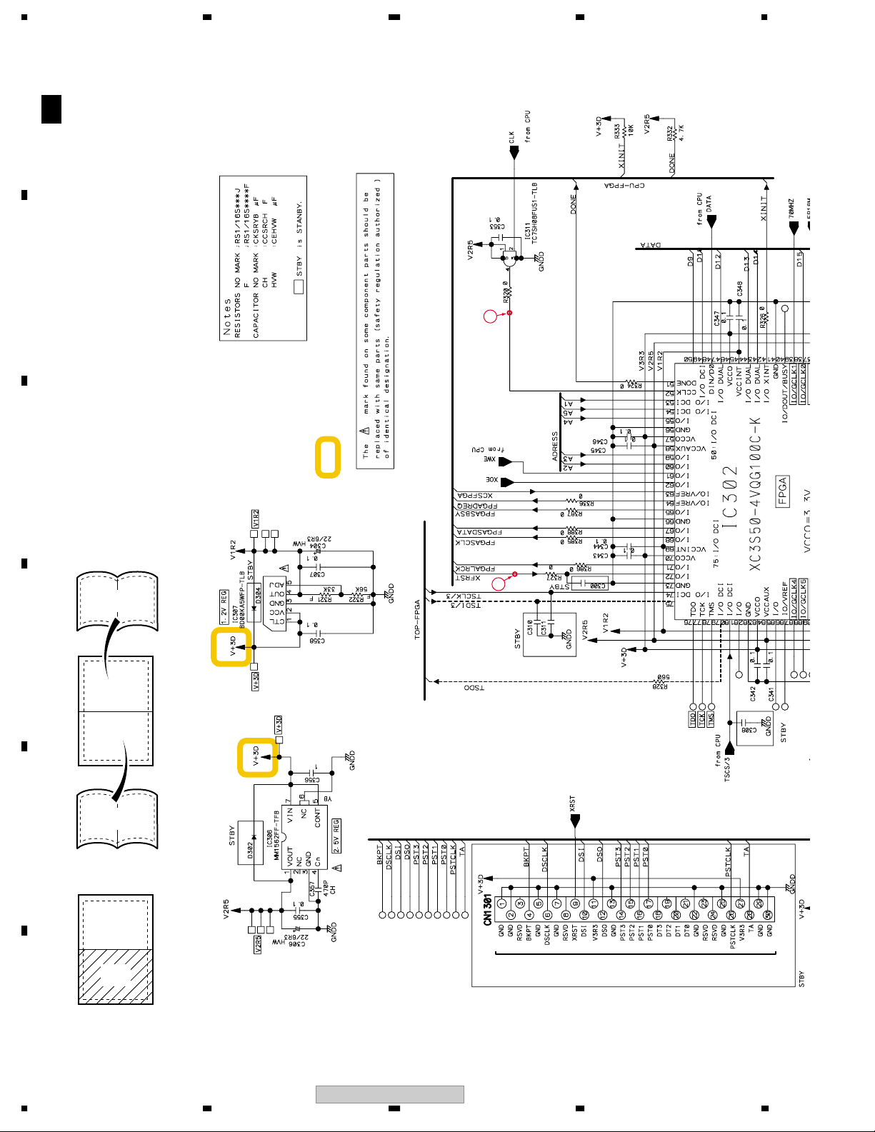
3.3 BLOCK DIAGRAM (Power)
• Power Delivery Map
A
Loading
M
GNDMGNDM
Motor Drive
GNDMGNDM
MAIN ASSY
DWG1622-A/J
5A
IC704 <0.3A
DAC
TRAVERS
MECHA
B
Spindle
SLED
M
M
Pickup ASSY
C
DWX2602-A/J
Stby
RLYB ASSY
GNDSGNDS
SLMB ASSY
DWS1388-A/J ServoDSP 83
REGB ASSY
DWR1310-A/J
GNDDGNDD
V+7M V+8A V+5P V+6B
GNDMGNDM
GNDDGNDD
V+3D
+1.2D
IC307 <0.6A FPGA (SPARTAN3)FPGA (SPARTAN3)
1.25D
IC703 <0.6A DSP
1.8D
IC305 <0.5A CPU (AMADEUS)CPU (AMADEUS)
2.5D
IC306 <0.5A FPGA (SPARTAN3)FPGA (SPARTAN3)
3.3S
IC100 <x.x0.6A LD 80
GNDDGNDD
GNDSGNDS
CUP 21 FPGA 60 DSP 5CUP 21 FPGA 60 DSP 5
SDRAM 22 FLASH 5SDRAM 22 FLASH 5
MUTE
GNDSGNDS
SECB
DWR13
D
E
F
+3.3D
+7A
TRNS ASSY
V+6
UnReg
V+10
UnReg
Vload
+32V
Transformer
FLAC_D
FLAC_J
ACIN ASSY
IC91 <
<1.0A
IC92
<1.0A
IC23,24IC23,24
<3.5A<3.5A
IC21,22IC21,22
<5.0A<5.0A
IC25IC25
<630mA<630mA
ICP
<1.0A
IC56
<800mA IC53
<1.5A IC54
IC57 <1.0A
+5P
<1A IC50
+8A
<0.8A IC61
<200mA
IC58 IC59
3.3V
3.3V
Q53
Regurator supporting Current Shutdown
ICP <200mA IC60
<200mA
C52
DATA Cntrol
-7
15W POINT
IC Protect
Pori SW
FUSE
MAX SPEC
A
ICP
Before REG-IC
GND
Screw (Chasis GND
20
CDJ-800MK2
1234
Page 21
GNDSGNDS
5678
A
<0.3A
6A FPGA (SPARTAN3)FPGA (SPARTAN3)
6A DSP
5A CPU (AMADEUS)CPU (AMADEUS)
5A FPGA (SPARTAN3)FPGA (SPARTAN3)
DAC
CUP 21 FPGA 60 DSP 5CUP 21 FPGA 60 DSP 5
SDRAM 22 FLASH 5SDRAM 22 FLASH 5
ServoDSP 83
LD 80
SECB ASSY
DWR1309-A/J
MUTE
GNDSGNDS
-7
<1.0A IC51
JACK ASSY
GNDAGNDA
GNDDGNDD
DWG1626-A/J
OP
AMP
GNDDGNDD
Stby
KSWB ASSY
SW
V+5P V+7
GNDADGNDAD
SW
L
R
D
DWS1386-A/J
LED
LED
GNDDGNDD
Jack
DFLB ASSY
DWG1623-A/J
EarthPlate
ChasisGND
SLDB ASSY
SLDB ASSY
DWS1387-A/J
DWS1387-A/J
GNDDGNDDGNDD
GNDFGNDF
GNDFGNDF
Vol
LED
VYNIL
B
C
D
DATA Cntrol
15W POINT
Before REG-IC
GND
Screw (Chasis GND)
56
C506 C506
GNDDGNDD
DISPLAY
MPU
GNDADGNDAD
DATA FL
GNDDGNDD
GNDDGNDD
V+5P
JOG
FL
<200mA IC603
Q604 DWG1624-A/J
JFLB ASSY
CDJ-800MK2
7
SW
SLIDER
JOGB ASSY
DWG1625-A/J
Rotation Detect
8
E
F
21
Page 22

1234
3.4 OVERALL WIRING DIAGRAM
A
B
C
SLOT-IN
D
SLMB ASSY
M
ACIN ASSY
E
E
RLYB ASSY
B
D
TRNS ASSY
SECB ASSY
C
ACIN ASSY
E
F
22
1234
CDJ-800MK2
REGB ASSY
F
Page 23

5678
MAIN ASSY
A
A A( 1/3 – 3/3)
JACK ASSY
I
A
B
C
DFLB ASSY
G
JFLB ASSY
K
JOGB ASSY
L
D
SLDB ASSY
J
E
KSWB ASSY
H
56
CDJ-800MK2
F
23
7
8
Page 24
1234
3.5 MAIN (1/3) and RLYB ASSYS
A
A 1/3
MAIN ASSY (DWG1622)
B
(TS)
(F)
(TS)
(TS)
(TS)
(F)
C
(RF)
(RF)
(RF)
(RF)
(RF)
(RF)
(RF)
(RF)
(F)
(RF)
(F)
(RF)
(F)
(RF)
(F)
(TD)
(TD)
D
(S)
(S)
(S)
E
to SPINDLE MOTOR
(S)
(S)
(S)
(TS)
(TS)
(F)
(F)
(S)
(S)
(TS)
(F)
(F)
(TS)
F
A 1/3
24
CDJ-800MK2
1234
Page 25
(RF)
(RF)
(RF)
(RF)
(TD)
(TD)
5678
(RF)
: RF DATA SIGNAL ROUTE
(TD)
: TRACKING DATA SIGNAL ROUTE
(F)
: FOCUS SERVO LOOP LINE
(TS)
: TRACKING SERVO LOOP LINE
(S)
: STEPPING SERVO LOOP LINE
to PICK UP ASSY (CN1)
A
B
C
(TS)
(TS)
(F)
(F)
CN1901
M
(S)
(S)
(S)
to LOADING MOTOR
D
to STEPPER MOTOR
(S)
RLYB ASSY
B
(DWX2602)
E
: The Power supply is shown with the marked box.
CDJ-800MK2
56
F
A 1/3
B
25
7
8
Page 26
1234
3.6 MAIN ASSY(2/3)
A 2/3
A
Large size
SCH diagram
B
C
MAIN ASSY (DWG1622) (1/2)
1/2
2/2
C
CN53
22
1/2
D
E
18
F
26
1234
71
CDJ-800MK2
Page 27
5678
A
B
24
27
26
C
91
D
56
CDJ-800MK2
36
E
MODE
MODE
F
27
7
8
Page 28
A
A 2/3
B
1234
MAIN ASSY (DWG1622) (2/2)
25
: The Power supply is shown with the marked box.
C
Large size
SCH diagram
30
1/2
D
2/2
E
to ICE BOARD
2/2
F
28
1234
CDJ-800MK2
Page 29
5678
A
B
23
C
D
E
56
CDJ-800MK2
: PANEL DATA (Digital)
: AUDIO DATA (Digital)
: AUDIO Lch OUT (Analog)
: DIGITAL AUDIO OUT (Digital)
F
29
7
8
Page 30
1234
3.7 MAIN ASSY(3/3)
A 3/3
A
B
C
MAIN ASSY (DWG1622)
31
32
34
D
21
29
E
F
A 3/3
30
CDJ-800MK2
1234
Page 31

5678
A
70
46
41
42
43
33
44
39
45
B
C
D
35
: The Power supply is shown with the marked box.
CDJ-800MK2
56
E
F
A 3/3
31
7
8
Page 32

1234
3.8 AC IN, TRNS, SECB and REGB ASSYS
ACIN ASSY
A
B
C
E
E
ACIN ASSY
DWR1439 (KUCXJ)
DWR1429 (WYXJ5)
DWR1432 (RLFXJ)
TRNS ASSY
D
DWR1371 (KUC, WY)
DWR1428 (RLF)
D
E
F
32
DE
CDJ-800MK2
1234
Page 33

5678
SECB ASSY (DWR1309)
C
REGB ASSY
F
A
B
CN802
I
CN301
2/3
A
C
CN501
G
D
E
59
: The Power supply is shown with the marked box.
CDJ-800MK2
56
58
F
C F
33
7
8
Page 34

1234
3.9 DFLB, JACK and KSWB ASSYS
A
DFLB ASSY (DWG1623)
G
50
73
B
CN56
C
53
51
52
48
74
56
57
55
54
C
D
49
E
72
F
G
34
1234
CDJ-800MK2
Page 35

5678
CN600
K
KSWB ASSY
H
(DWS1386)
A
B
C
CN701
3/3
A
CN50
C
JACK ASSY (DWG1626)
I
47
40
D
E
CN1503
: The Power supply is shown with the marked box.
J
: PANEL DATA (Digital)
: AUDIO DATA (Digital)
: AUDIO Lch OUT (Analog)
: DIGITAL AUDIO OUT (Digital)
56
CDJ-800MK2
F
H
7
8
I
35
Page 36

1234
3.10 JFLB, SLDB, SLMB and JOGB ASSYS
A
B
C
D
60
61
62
63
CN500
G
E
64
65
66
(DSX1065)
to Sheet SW
CN1601
L
JFLB ASSY (DWG1624)
K
F
K
36
1234
CDJ-800MK2
Page 37

5678
CN503
CN503
G
G
68
68
67
67
: The Power supply is shown with the marked box.
: The Power supply is shown with the marked box.
69
69
A
B
C
CN601
CN601
K
K
JOGB ASSY (DWG1625)
JOGB ASSY (DWG1625)
L
L
SLDB ASSY (DWS1387)
SLDB ASSY (DWS1387)
J
J
CN1105
CN1105
B
B
SLMB ASSY (DWS1388)
SLMB ASSY (DWS1388)
M
M
D
E
F
56
CDJ-800MK2
LJ M
LJ M
37
7
8
Page 38

1234
3.11 WAVEFORMS
Note : The encircled numbers denote measuring point in the schematic diagram.
A
B
C
A
MAIN ASSY
1/2
• at play
RFO
1
V: 500mV/div. H: 200nsec/div.
• at play
AGCRF
2
V: 500mV/div. H: 200nsec/div.
• at load-out
LPS1
3
V: 5V/div. H: 500msec/div.
LPS2
4
V: 5V/div. H: 500msec/div.
LO+
5
V: 5V/div. H: 500msec/div.
LO–
6
V: 5V/div. H: 500msec/div.
3
4
5
6
• at focus-in
FE
7
V: 5V/div. H: 2msec/div.
• at start-up
FE
7
V: 1V/div. H: 200msec/div.
TE
9
V: 1V/div. H: 200msec/div.
DMO
10
V: 1V/div. H: 200msec/div.
INSIDE
11
V: 5V/div. H: 200msec/div.
7
9
10
11
• at stopped
FE
7
V: 1V/div. H: 100msec/div.
TE
9
V: 1V/div. H: 100msec/div.
DMO
10
V: 1V/div. H: 100msec/div.
LDO
12
V: 5V/div. H: 100msec/div.
D
E
F
• at load-in
LPS1
3
V: 5V/div. H: 200msec/div.
LPS2
4
V: 5V/div. H: 200msec/div.
LO+
5
V: 5V/div. H: 200msec/div.
LO–
6
V: 5V/div. H: 200msec/div.
3
4
5
6
• at focus-in
FE
7
V: 5V/div. H: 100msec/div.
FOO
8
V: 5V/div. H: 100msec/div.
7
8
7
9
10
12
• at auto adjustment
FE
7
V: 1V/div. H: 200msec/div.
FOO
8
V: 1V/div. H: 200msec/div.
TE
9
V: 1V/div. H: 200msec/div.
TRO
13
V: 2V/div. H: 200msec/div.
7
8
9
13
38
CDJ-800MK2
1234
Page 39

5678
A
MAIN ASSY
1/2
• at pause
TE
9
V: 1V/div. H: 2msec/div.
TRO
13
V: 2V/div. H: 2msec/div.
RFO
1
V: 1V/div. H: 2msec/div.
SBOK
14
V: 5V/div. H: 2msec/div.
9 9
13
1
14
• at scan
TE
9
V: 1V/div. H: 2msec/div.
TRO
13
V: 1V/div. H: 2msec/div.
RFO
1
V: 1V/div. H: 2msec/div.
SBOK
14
V: 5V/div. H: 2msec/div.
• at play
TE
9
V: 1V/div. H: 1sec/div.
TRO
13
V: 2V/div. H: 1sec/div.
ST1 (IC109-pin 1)
15
V: 1V/div. H: 1sec/div.
ST2 (IC109-pin 2)
16
V: 1V/div. H: 1sec/div.
13
15
16
• at scan
TE
9
V: 1V/div. H: 50msec/div.
TRO
13
V: 2V/div. H: 50msec/div.
ST1 (IC109-pin 1)
15
V: 1V/div. H: 50msec/div.
ST2 (IC109-pin 2)
16
V: 1V/div. H: 50msec/div.
A
B
C
9
13
1
14
• at track search
TE
9
V: 1V/div. H: 50msec/div.
TRO
13
V: 1V/div. H: 50msec/div.
RFO
1
V: 1V/div. H: 50msec/div.
SBOK
14
V: 5V/div. H: 50msec/div.
9
13
1
9
13
15
16
• at track search
TE
9
V: 1V/div. H: 20msec/div.
TRO
13
V: 2V/div. H: 20msec/div.
ST1 (IC109-pin 1)
15
V: 2V/div. H: 20msec/div.
ST2 (IC109-pin 2)
16
V: 2V/div. H: 20msec/div.
9
13
15
D
E
14
16
CDJ-800MK2
56
7
8
F
39
Page 40

1234
Note : The encircled numbers denote measuring point in the schematic diagram.
A
B
C
A
MAIN ASSY
1/2
• at play
RFO
1
V: 500mV/div. H: 200nsec/div.
• at play
AGCRF
2
V: 500mV/div. H: 200nsec/div.
• at load-out
LPS1
3
V: 5V/div. H: 500msec/div.
LPS2
4
V: 5V/div. H: 500msec/div.
LO+
5
V: 5V/div. H: 500msec/div.
LO–
6
V: 5V/div. H: 500msec/div.
3
4
5
6
• at focus-in
FE
7
V: 5V/div. H: 2msec/div.
• at start-up
FE
7
V: 1V/div. H: 200msec/div.
TE
9
V: 1V/div. H: 200msec/div.
DMO
10
V: 1V/div. H: 200msec/div.
INSIDE
11
V: 5V/div. H: 200msec/div.
7
9
10
11
• at stopped
FE
7
V: 1V/div. H: 100msec/div.
TE
9
V: 1V/div. H: 100msec/div.
DMO
10
V: 1V/div. H: 100msec/div.
LDO
12
V: 5V/div. H: 100msec/div.
D
E
F
• at load-in
LPS1
3
V: 5V/div. H: 200msec/div.
LPS2
4
V: 5V/div. H: 200msec/div.
LO+
5
V: 5V/div. H: 200msec/div.
LO–
6
V: 5V/div. H: 200msec/div.
3
4
5
6
• at focus-in
FE
7
V: 5V/div. H: 100msec/div.
FOO
8
V: 5V/div. H: 100msec/div.
7
8
7
9
10
12
• at auto adjustment
FE
7
V: 1V/div. H: 200msec/div.
FOO
8
V: 1V/div. H: 200msec/div.
TE
9
V: 1V/div. H: 200msec/div.
TRO
13
V: 2V/div. H: 200msec/div.
7
8
9
13
40
CDJ-800MK2
1234
Page 41

5678
A
MAIN ASSY
1/2
• at pause
TE
9
V: 1V/div. H: 2msec/div.
TRO
13
V: 2V/div. H: 2msec/div.
RFO
1
V: 1V/div. H: 2msec/div.
SBOK
14
V: 5V/div. H: 2msec/div.
9 9
13
1
14
• at scan
TE
9
V: 1V/div. H: 2msec/div.
TRO
13
V: 1V/div. H: 2msec/div.
RFO
1
V: 1V/div. H: 2msec/div.
SBOK
14
V: 5V/div. H: 2msec/div.
• at play
TE
9
V: 1V/div. H: 1sec/div.
TRO
13
V: 2V/div. H: 1sec/div.
ST1 (IC109-pin 1)
15
V: 1V/div. H: 1sec/div.
ST2 (IC109-pin 2)
16
V: 1V/div. H: 1sec/div.
13
15
16
• at scan
TE
9
V: 1V/div. H: 50msec/div.
TRO
13
V: 2V/div. H: 50msec/div.
ST1 (IC109-pin 1)
15
V: 1V/div. H: 50msec/div.
ST2 (IC109-pin 2)
16
V: 1V/div. H: 50msec/div.
A
B
C
9
13
1
14
• at track search
TE
9
V: 1V/div. H: 50msec/div.
TRO
13
V: 1V/div. H: 50msec/div.
RFO
1
V: 1V/div. H: 50msec/div.
SBOK
14
V: 5V/div. H: 50msec/div.
9
13
1
9
13
15
16
• at track search
TE
9
V: 1V/div. H: 20msec/div.
TRO
13
V: 2V/div. H: 20msec/div.
ST1 (IC109-pin 1)
15
V: 2V/div. H: 20msec/div.
ST2 (IC109-pin 2)
16
V: 2V/div. H: 20msec/div.
9
13
15
D
E
14
16
CDJ-800MK2
56
7
8
F
41
Page 42

1234
3.12 VOLTAGES
Note : Amplitude measurement is device control measured value of the pseudo that used digital circuit tester (HOZAN DT-113).
Because dispersion appears with circuit tester that it is waveform with much AC component, please pay attention.
A
Measurement condition : CD play status ( A testing disc STD -905 truck 2 play made in Pioneer)
# IC of SECB ASSY mounting measures it with the condition which excluded connected load after SECB ASSY.
# Voltage value of MPU(MAIN ASSY IC301) measures it by standby status (it is not a CD play).
The reason is because it is it in the CD status that cannot play (Frieze) that this is failure of core block and is by this status as the
condition that I put together.
# IC303(SDRAM), IC101(ServoDSP), IC312(Logic), IC311(Logic), IC103(OPAMP), IC310(Logic) of MAIN ASSY || for B surface mount,
I measure it by the status that pulled FFC between MAIN-JACK.
MAIN ASSY
IC100 NJM2885DL1-33
Pin No.
B
IC103 NJU7013F
Pin No.
IC104 NJM2903M
C
Pin No.
IC105 TC7W04FU
Pin No.
D
IC106 TC7W08FU
Pin No.
E
Voltage (V)
1
2
3
Voltage (V)
1
2
3
4
5
Voltage (V)
1
2
3
4
5
6
7
8
Voltage (V)
1
2
3
4
5
6
7
8
Voltage (V)
1
2
3
4
5
6
7
8
6.0
0.00
3.3
0.2
0.0
0.2
0.2
3.3
3.1
1.7
1.8
0.0
1.7
1.7
1.5
3.3
0.0
1.7
0.0
0.0
3.3
1.6
3.3
3.3
3.3
0–3.2
0–3.2
0.0
0–3.2
0–3.2
0–3.2
3.3
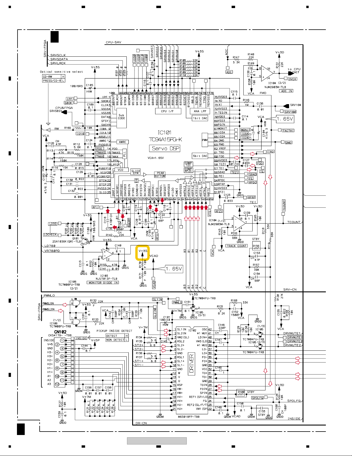
IC101 TC94A15FG
Pin No.
1
2
3
4
5
6
7
8
9
10
11
12
13
14
15
16
17
18
19
20
21
22
23
24
25
26
27
28
29
30
31
32
33
34
35
36
37
38
39
40
41
42
43
44
45
46
47
48
49
50
Voltage (V)
0.0
2.9–3.3
0.0
3.3
0.0
0.0
0.0
0.0
0.0
0.0
3.3
0.0
3.3
1.6
1.6
1.6
1.6
1.4
1.6
0.6
1.6
1.6
1.6
0.0
1.7
1.6
1.6
1.6
3.3
1.5
1.6
1.5
1.6
0.0
1.6
1.3
1.3
3.3
0.0
3.3
2.4
0.2
0.0
1.8
1.7
1.7
1.7
1.8
1.8
IC102 M63018FP
Pin No. Voltage (V)
51
52
53
54
55
56
57
58
59
60
61
62
63
64
65
66
67
68
69
70
71
72
73
74
75
76
77
78
79
80
81
82
83
84
85
86
87
88
89
90
91
92
93
94
95
96
97
98
99
–
100
1.6
0.0
2.4
1.6
1.5
1.8
1.7
1.6
3.3
1.6
1.6
1.6
1.6
2.0
0.0
0.0
0.7–1.0
0.0
0.0
3.3
0.0
0.0
1.6
1.5
3.3
0.0
1.6
3.3
0.0
1.6
0.0
0.0
0.0
3.2
3.2
3.2
3.2
3.2
2.8–3.0
3.3
3.3
1.8–2.4
3.3
0.0
3.3
0.0
1.7
1.7
1.7
0.0
Pin No.
1
2
3
4
5
6
7
8
9
10
11
12
13
14
15
16
17
18
19
20
21
22
23
24
25
26
27
28
29
30
31
32
33
34
35
36
37
38
39
40
41
42
Voltage (V)
1.0–2.5
1.0–2.5
7.1
7.1
0–7
0–7
0.0
7.1
0–7
0–7
0.0
0.5–1.2
0.5–1.2
0.5–1.2
7.1
2.5
2.5
2.5
2.5
2.5
2.5
7.1
1.7
1.6
1.7
1.7
1.7
1.7
0.0
3.1
3.1
7.1
0.0
3.1
3.1
1.1
1.1
3.3
7.1
1.7
3.3
1.1
IC300 DYW1753-B/J
Pin No. Voltage (V)
1
2
3
4
5
6
7
8
9
10
11
12
13
14
15
16
17
18
19
20
21
22
23
24
25
26
27
28
29
30
31
32
33
34
35
36
37
38
39
40
41
42
43
44
45
46
47
48
2.2
2.1–2.4
0.9–1.2
1.7–2.0
1.7–1.9
1.9–2.2
2.0–2.2
2.1–2.4
0.0
0.0
2.5–2.8
3.3
0.0
0.0
3.3
0.5
1.2–1.5
2.1–2.4
2.1–2.4
1.8–2.2
1.9–2.2
1.9–2.2
0.9–1.1
2.1–2.4
1.9
3.3
0.0
3.3
0.0
3.3
0.5–0.8
0.5–0.9
0.5–0.8
0.5–0.8
0.5–0.8
0.4–0.7
3.3
0.7–0.8
0.6–0.8
0.6–0.8
0.8–1.0
0.5–0.7
0.4–0.6
0.6–0.7
0.5–0.7
0.0
3.3
1.3–1.5
F
42
1234
CDJ-800MK2
Page 43

5678
IC301 SCF5249VM140
Pin No. Voltage (V)
A1
A2
A3
A4
A5
A6
A7
A8
A9
A10
A11
A12
A13
A14
B1
B2
B3
B4
B5
B6
B7
B8
B9
B10
B11
B12
B13
B14
C1
C2
C3
C4
C11
C12
C13
C14
D1
D2
D3
D4
D5
D6
D7
D8
D9
D10
D11
D12
D13
D14
E1
E2
E3
E4
E5
E6
E7
E8
E9
E10
E11
E12
E13
E14
F1
3.3
3.3
2.3
2.4
2.4
3.3
0.0
3.3
3.3
0.0
2.7
3.3
0.0
0.0
2.3
2.0
2.3
2.4
0.9
2.1
3.3
0.0
3.3
0.0
3.3
0.0
3.2
0.0
2.4
2.1
0.0
1.8
3.3
2.2
0.0
0.0
1.2
1.1
0.3
0.0
0.0
0.0
3.3
0.0
0.0
0.0
0.0
0.0
0.0
0.0
3.3
1.7
0.0
2.7
3.3
0.0
3.3
3.3
1.8
0.0
0.0
0.0
0.0
0.0
0.0
Pin No. Voltage (V)
F2
F3
F4
F11
F12
F13
F14
G1
G2
G3
G4
G11
G12
G13
G14
H1
H2
H3
H4
H11
H12
H13
H14
J1
J2
J3
J4
J11
J12
J13
J14
K1
K2
K3
K4
K5
K6
K7
K8
K9
K10
K11
K12
K13
K14
L1
L2
L3
L4
L5
L6
L7
L8
L9
L10
L11
L12
L13
L14
M1
M2
M3
M4
M11
M12
0.3
3.2
0.0
0.0
0.0
3.3
0.0
0.5
0.5
0.8
0.0
3.3
0.0
0.0
0.0
0.4
0.6
0.0
0.0
1.8
3.2
3.3
1.6
0.7
0.4
3.2
0.0
0.0
3.3
0.0
0.0
0.5
2.0
0.0
0.0
0.0
1.8
0.5
3.3
0.0
0.0
0.0
0.0
0.0
0.0
0.9
2.4
3.3
3.3
3.3
3.3
4.9
0.0
4.4
1.8
0.0
3.2
1.6
3.3
2.3
0.6
0.0
0.0
3.3
0.0
Pin No. Voltage (V)
M13
M14
N1
N2
N3
N4
N5
N6
N7
N8
N9
N10
N11
N12
N13
N14
P1
P2
P3
P4
P5
P6
P7
P8
P9
P10
P11
P12
P13
P14
3.2
1.5
0.7
1.2
3.0
3.3
0.0
0.6
0.4
0.0
0.0
3.3
1.7
3.3
2.5
1.7
3.0
2.6
0.0
3.3
3.3
3.3
0.6
0.5
0.0
1.5
0.0
3.3
3.3
3.3
IC302 XC3S50-4VQG100C
Pin No. Voltage (V)
1
2
3
4
5
6
7
8
9
10
11
12
13
14
15
16
17
18
19
20
21
22
23
24
25
26
27
28
29
30
31
32
33
34
35
36
37
38
39
40
41
42
43
44
45
46
47
48
49
50
0–1.8
1.6
0.0
3.2
0.0
3.3
2.5
0.0
1–4.5
0.0
1–4.5
1.6
1.6–1.8
1.7
1.7
1.8
1.9
1.2
3.3
0.0
0.5–0.7
0.5–0.7
0.5–0.7
2.5
2.5
2.5
0.7–0.9
0.7–0.9
0.0
0.5–0.7
3.3
0.4–0.7
2.5
0.6–0.9
0.4–0.8
0.5–0.7
1.6
0.5–0.7
1.7
0.0
0.0
3.3
0.5–0.7
0.8–1.0
1.2
3.3
0.6–0.8
0.0
0.5–0.8
0.5–0.8
Pin No. Voltage (V)
51
52
53
54
55
56
57
58
59
60
61
62
63
64
65
66
67
68
69
70
71
72
73
74
75
76
77
78
79
80
81
82
83
84
85
86
87
88
89
90
91
92
93
94
95
96
97
98
99
100
2.5
0.0
2.0
1.9–2.2
0.0
0.0
3.3
2.5
0.9
2.4
2.8
0.0
3.3
3.3
0.0
0.0
1.6
1.7
1.2
3.3
1.6
3.3
0.0
3.2
0.2
2.5
2.5
2.5
0.0
2.7
0.0
0.0
3.3
2.5
0.0
0.0
0.0
0.0
0.0
0.0
0.0
0.0
1.2
3.3
0.0
0.0
0.0
0.0
2.5
2.5
A
B
C
D
E
F
56
CDJ-800MK2
43
7
8
Page 44

1234
IC303 K4S641632H-TC75
Pin No. Voltage (V)
A
B
C
D
E
1
2
3
4
5
6
7
8
9
10
11
12
13
14
15
16
17
18
19
20
21
22
23
24
25
26
27
28
29
30
31
32
33
34
35
36
37
38
39
40
41
42
43
44
45
46
47
48
49
50
51
52
53
54
IC304 BU4230G
Pin No. Voltage (V)
1
2
3
4
5
0.5–0.7
0.6–0.9
0.6–0.8
0.7–0.8
0.6–0.9
0.7–0.9
0.6–0.8
0.9–1.1
0.4–0.8
0.9–1.1
1.7–1.9
1.7–1.9
1.9–2.2
2.0–2.2
2.1–2.4
1.3–1.6
1.2–1.5
0.8–1.1
0.5–0.7
0.5–0.8
0.5–0.8
0.4–0.7
0.8–1.0
0.5–0.7
0.5–0.8
3.3
0.0
3.3
0.0
3.3
0.0
3.3
0.0
3.0
2.6
2.8
1.2
0.6
0.0
2.3
3.3
0.0
0.0
3.3
1.7
0.1
0.0
0.0
3.3
0.0
3.3
3.3
0.0
0.0
3.3
3.3
0.0
0.0
1.7
IC305 MM1561JF
Pin No. Voltage (V)
1
2
3
4
5
6
7
IC306 MM1562FF
Pin No. Voltage (V)
1
2
3
4
5
6
7
IC307 BD00KA5WFP
Pin No. Voltage (V)
1
2
3
4
5
IC308 TC74VHC08FTS1
Pin No. Voltage (V)
1
2
3
4
5
6
7
8
9
10
11
12
13
14
IC309 TC7SET08FUS1
Pin No. Voltage (V)
1
2
3
4
5
IC310 TC7WU04FU
Pin No. Voltage (V)
1
2
3
4
5
6
7
8
1.8
0.0
0.0
0.5
3.3
0.0
3.3
2.5
0.0
0.0
1.2
3.3
0.0
3.3
3.3
3.3
0.0
1.2
0.8
3.3
4.8
3.2
3.3
4.3
2.9
0.0
0.0
3.3
0.0
2.7
3.3
4.0
3.3
4.9
3.3
0.0
4.9
4.9
1.6
1.6
1.6
0.0
1.6
1.6
1.6
3.3
IC311 TC7SH08FUS1
Pin No. Voltage (V)
1
2
3
4
5
IC312 TC7SH08FUS1
Pin No. Voltage (V)
1
2
3
4
5
IC702 PE8001A
Pin No. Voltage (V)
1
2
3
4
5
6
7
8
9
10
11
12
13
14
15
16
17
18
19
20
21
22
23
24
25
26
27
28
IC703 BD00KA5WFP
Pin No. Voltage (V)
1
2
3
4
5
IC704 NJM2880U1-05
Pin No. Voltage (V)
1
2
3
4
5
2.5
0.0
0.0
0.0
2.5
2.5
3.3
0.0
2.5
2.5
1.6
0.0
1.6
0.0
1.6
0.0
0.0
5.0
5.0
0.0
2.5
0.0
2.5
0.0
5.0
2.5
0.0
2.5
0.0
5.0
3.3
5.0
0.0
0.0
0.0
0.0
0.0
3.3
3.3
3.3
0.0
1.3
0.8
8.0
0.0
1.3
5.0
8.0
IC701 DSPC56371AF180
Pin No. Voltage (V)
1
2
3
4
5
6
7
8
9
10
11
12
13
14
15
16
17
18
19
20
21
22
23
24
25
26
27
28
29
30
31
32
33
34
35
36
37
38
39
40
0.0
0.0
3.3
0.0
0.0
0.0
0.8
1.3
0.0
0.0
0.0
0.0
0.0
0.0
0.0
0.0
3.3
0.0
0.0
0.0
0.0
0.0
3.3
0.0
3.3
0.0
0.0
0.0
1.3
1.1
3.0
0.0
3.0
0.0
2.6
0.0
3.3
0.0
3.3
0.0
Pin No. Voltage (V)
41
42
43
44
45
46
47
48
49
50
51
52
53
54
55
56
57
58
59
60
61
62
63
64
65
66
67
68
69
70
71
72
73
74
75
76
77
78
79
80
3.3
0.0
0.0
1.3
1.7–1.8
1.2
3.3
0.6
3.3
0.6
3.3
1.3
0.0
0.0
0.0
0.0
0.0
0.0
1.0
3.2
1.6
0.0
1.7
3.3
0.0
0.0
0.0
0.0
1.6
1.6
1.3
0.0
1.6
0.0
3.3
1.7
1.6
1.6
1.6
0.0
F
44
1234
CDJ-800MK2
Page 45

5678
SECB ASSY
IC050 BA00BC0WCP-V5
Pin No. Voltage (V)
1
2
3
4
5
IC051 NJM2374AM
Pin No. Voltage (V)
1
2
3
4
5
6
7
8
IC052 TC7S04FU
Pin No. Voltage (V)
1
2
3
4
5
IC057 BA50BC0WFP
Pin No. Voltage (V)
1
2
3
4
5
12.3
12.3
0.0
8.0
1.3
8.0
-2.7
-6.1
-7.0
-5.7
8.1
8.0
8.0
0.0
0.0
0.0
2.7
5.0
8.0
8.0
0.0
5.0
0.0
REGB ASSY
IC091 BA00BC0WCP-V5
Pin No. Voltage (V)
1
2
3
4
5
IC092 BA00BC0WCP-V5
Pin No. Voltage (V)
1
2
3
4
5
6.0
6.0
0.0
3.3
1.3
11.2
11.2
0.0
7.2
1.3
DFLB ASSY
IC501 PEG237B
Pin No. Voltage (V)
1
2
3
4
5
6
7
8
9
10
11
12
13
14
15
16
17
18
19
20
21
22
23
24
25
26
27
28
29
30
31
32
33
34
35
36
37
38
39
40
41
42
43
44
45
46
47
48
49
50
0.0
0.0
0.0
0.0
0.0
4.9
0.0
0.0
0.0
0.0
0.0
4.5
2.6
0.0
2.3
5.0
5.0
5.0
5.0
5.0
5.0
5.0
5.0
4.9
4.9
0.0
4.9
3.9
0.0
1.4–1.8
0.8
4.9
4.5
4.9
4.3
0.1
4.8
4.0
4.9
0.0
0.0
0.0
0.6
0.0
2.8
4.9
0.0
4.9
4.9
0.0
Pin No. Voltage (V)
51
52
53
54
55
56
57
58
59
60
61
62
63
64
65
66
67
68
69
70
71
72
73
74
75
76
77
78
79
80
81
82
83
84
85
86
87
88
89
90
91
92
93
94
95
96
97
98
99
100
0.0
4.9
4.9
4.9
4.9
4.9
0.0
4.9
0.0
0.0
0.0
4.9
0.0
0.0
0.0
0.0
0.0
0.0
0.0
0.0
0.0
0.0
0.0
0.0
0.0
0.0
0.0
0.0
4.9
4.9
4.9
4.9
4.9
4.9
4.9
4.9
4.9
4.9
2.5
2.5
4.9
4.9
4.9
4.9
4.9
0.0
0.0
4.9
4.9
4.9
IC502 BU4242G
Pin No. Voltage (V)
1
2
3
4
5
IC503 TC7SET08FUS1
Pin No. Voltage (V)
1
2
3
4
5
4.5
4.9
0.0
0.0
2.6
4.9
0.0
0.0
0.1
4.9
JACK ASSY
IC801 NJM4558DX
Pin No. Voltage (V)
1
2
3
4
5
6
7
8
0.0
0.0
0.0
-6.0
0.0
0.0
0.0
8.0
A
B
C
D
56
CDJ-800MK2
E
F
45
7
8
Page 46

1234
A
B
C
D
E
F
46
1234
CDJ-800MK2
Page 47

5678
4. PCB CONNECTION DIAGRAM
NOTE FOR PCB DIAGRAMS :
1. Part numbers in PCB diagrams match those in the schematic
diagrams.
2. A comparison between the main parts of PCB and schematic
diagrams is shown below.
Symbol In PCB
Diagrams
BCE
BCE
D
Symbol In Schematic
Diagrams
BCEBCE
BCE
DGGSS
BCE
DGS
Part Name
Transistor
Transistor
with resistor
Field effect
transistor
Resistor array
3-terminal
regulator
3. The parts mounted on this PCB include all necessary parts for
several destinations.
For further information for respective destinations, be sure to
check with the schematic diagram.
4. View point of PCB diagrams.
Connector
Capacitor
SIDE A
P.C.Board
Chip Part
SIDE B
A
B
C
D
E
F
56
CDJ-800MK2
47
7
8
Page 48

1234
5
4
R151
C
R
D
SBOK
2
2
4.1 MAIN ASSY
SIDE A
A
MAIN ASSY
A
SPINDLE MOTOR
CN102
CONTACT SIDE=UP
IC308
14
R317
TP31
C313
R338
H2-
C317
R377
R306
C312
DONE
R378
R370
TP45
H3-
H3+
24
R359
TP39
R309
Q303
R310
R304
R373
R365
R361
TSDO
TSCS
Q301
3
XINT
R369
R358
C336
25
TSCLK
4
27
36
71
R356
TP1
C309
5
IC309
R382
TP42
CN102
B
C
GNDM
57
R303
A3
12
C320
A2
10
INSIDE
45
IC304
C303
18
IC305
A1
H1-
H1+
LF
C337
4
C302
C319
R318
3
R305
7
C318
8
RST
1
H2+
C321
R353
30
V1R8
D
TP28
FCICT
TP49
CN1301
R394
2
1
DNP2131-C
E
KN301
Production code
C358
1
2
AOI
R321
4
5
V1R2
C
R307
R308
R329
Q305
R375
R381
R376
CPU16M
14
TP14
R351
R354
30
IC307
R322
CN53
CN301
TSDI
Q302
GNDD
R301
Q304
26
R380
TP37
IC301
R336
R387
R388
R385
C343
R327
C311
C307
V+5PV+3D
PRGM
19
R374
R368
TP36
R350
51
IC302
C344
R386
C300
C310
5
C356
V+3DV2R5
22
C301
R731
Q705 Q706
R379
R323
48
R357
P
70M
R355
A
1
1
FP16M
50
75
76 100
R328
C308
C341
C342
4
7
IC306
C357
CONTACT SIDE=UP
R144
CN301
LPS1
1
V+8A
R339
R740
R738
R732
C340
R739
C339
R340
LPS2
R741
LD3S
C359
26
23
C355
R143
LDCHECK
C360
25
24
25
R383
R342
4
IC300
C333
R319
21
R752
IC104
C132
C131
C130
R112
C352
C334
C335
R347
R343
R753
R145
R150C138
C102
IO1A
R113
C126
R345
DSP16M
R302
29
R384
34
C718
C139
17
C128
R116
R114
R115
R109
31
C748
8
VCA
C129
C137
R107
R108
SPSIN
747
754
C746R747
780
IC304 IC308
F
IC305
IC308
Q303
IC304
IC305
Q303
Q305Q301 Q302
Q305
IC309
IC309
Q302Q301
Q304 Q705
IC307 IC306
A
48
CDJ-800MK2
IC302
IC302
IC301
IC301
Q706
Q705Q304
Q706
IC306IC307
IC300
IC104
IC300
IC104
1234
Page 49

5678
0
IC
C
7
R
SIDE A
A
CN1101
B
NOTE : The encircled numbers denote measuring point.
CN101
CONTACT SIDE
R145
C139
R151
ADC
C162
R147
8
R150C138
C102
17
IO1A
C128
R116
R114
R115
R113
C126
R109
31
DSP16M
C748
29
34
5
R148
Q101
R149
RW
VCA
C129
R108
C746
R747
AGCRF
2
RFI
C117
C124
PDO
SBOK
IO3B
20
IPF
C137
IO2B
R107
R106
R105
DSPSIN
32
C749
4021
41
C747
R754
60
61
R780
R748
R757
C755
V1R25
C757
4
IC1
C132
C131
C130
5
300
21
R752
R112
C352
R302
C334
C335
R34
R343
R753
R345
R384
C718
R101
R102
TACTHI
1
IC701
C756
C725
13
RFO
IO1B
R110
R159
R103
C116
R742
31
32
C113
R104
R701
B3
C103
IO0B
28
B4
B1
C106
FTE
SRV16M
44
C750
C751
80
43
C754
R743
A
B2
C
C123
TRO
IO2A
14
38
IC105
DRVMUTE2
PWMLO
DRVMUTE1
R700
20
41
R750
R749
TD
TRFDFR
RFZI
8
RFDC
C127
11
IO3A
C104
C151
37
4
5
4
C752
28
33
42
C758
R751
C753
FE
TE
R120
MONIT
DMO
8
5
R775
C732
11M
IC703
CN101
LO+
RFRP
SBAD
R119
12
5
C702
C731
39
35
ST2+
TEZI
C160
R130
C161
8
IC106
1
2
LO-
9
R118
R129
ST2-
FOO
V+6B
C700
ST1-
ST1+
C149
D100
45
VCAD
C163
C168
14
1/2
MAIN
SPDLFG
15
C734
DWG1645
DWG1622
C150
C148
R100
C164
2
C729
3
4
C730
C733
V5DAC
IC702
1
5
Lch
Rch
C101
R137
R136
R131
V+3S
C728
V-7A
IC704
MUTE
R134
R135
15
C152
C147
C146
16
IC100
R
70
DOUT
9
46
R
V+8A
L
MOTHER
V+7M
C145
SL1IN
IC102
C142
R154
C143
R155
R132
R133
SIDE_A
SL2IN
R164
REFLOW
1
DWM2276
DWM2232
KN701
(SECOND)
CN801
CN701
I
CN701
CONTACT SIDE=UP
B
C
D
E
0
IC104
0
IC104
Q101
Q101
IC701
IC703 IC702
IC105
IC106
IC105
IC704 IC100
IC702IC703 IC704IC106
IC100
IC701
CDJ-800MK2
56
IC102
IC102
(DNP2131-C)
7
F
A
49
8
Page 50

A
C373
C368
B
C
D
SIDE B
1234
MAIN ASSY
A
CN101
R138
R139
CN701
LF
C133
R165
C165
R168
C105
R121
R122
R123
R158
C154
R124
C155
R157
R125
D707
R126
R170
C153
R156
C100
C111
R171
IC101
51
C112
C114
C115
75
R146
C701
76
C136
R153
50
C167
R341
R152
C141
C121
C110
C122
IC103
4
153
C140
R163
C119
100
R162
R161
C120
26
R776
C108
R142
C107
R169
C135
25
C134
C109
C118
C166
C372
C370
R346
R344
C703
R389
C705
C706
R735
R736
Q707
Q707
Q707
C704
R733
R734
C743
IC101 IC103
C712
D705
IC103IC101
E
F
A
50
1234
CDJ-800MK2
Page 51

5678
SIDE B
A
CN301 CN102
C134
C1
C118
C166
R344
C372
R346
R389
C373
C370
C368
D307
D301
C157
C158
C156
SIDE_B_(FIRST)
B
C
D
E
C159
R349
R348
R127
0
1
R315R316
C316
C144
D305
D306
R300
R393
C315
R166
D104
D103
TP12
R366
45
TP11
R352
R320
25
R337
C338
C328
C324
TP30
R324
R312
IC311
R367
C305
R372
C332
4
3
C329
R333
C326
C325
C314
8
5
R391
C323
R360
R392
R313
IC310
R364
C330
R334
R325
R314
R371
X301
C304
R128
IC303
C361
C331
C363
TP19
C322
27
C351
C366
C350
R362
R330
R331
3
IC312
4
C354
5
C348
2854
C346
C345
R326
C347
R311
C353
D102
D101
0
0
123
1
0
C327
123456789
R363
CBA
R332
16M X'TAL
C306
D302
D304
IC311 IC310IC303
IC312
IC303
IC310IC311
NOTE : The encircled numbers denote measuring point.
IC312
CDJ-800MK2
56
(DNP2131-C)
F
A
51
7
8
Page 52

1234
4.2 RLYB ASSY
SIDE A SIDE A
A
RLYB ASSY
B
31
32
LF
4
B
A
CN101
CN1101
6
7
3
2
1
CN1101
24
C
C1106
HEAT PROOF PRE FLUX
C1104
CN1102
CONTACT SIDE=DOWN
PICKUP ASSY (CN1)
CN1102
1/2
1
C1109
C1108
D
R
SHORT CONTACT SIDE
LD
S1101
->
->
RLYB DWX2602
OPEN
1
LOADING MOTOR
CN1106
12
CN1105
E
13
4
CN1106
CN1105
CN1901
M
1
CONTACT SIDE
CN1104
(DNP2131-C)
NOTE : The encircled numbers denote measuring point.
F
B B
52
1234
CDJ-800MK2
Page 53

5678
SIDE B SIDE B
RLYB ASSY
B
LF
CN1101
A
B
C1107
C1105
C
CN1102CN1106CN1105
D
E
(DNP2131-C)
B B
56
CDJ-800MK2
7
8
F
53
Page 54

1234
E
N
4.3 SECB ASSY
SIDE A
A
B
C
SECB ASSY
C
KN51
49101.5
IC54
V+8
IC61
JA51
491.800
R74
SIDE
CHARACTER
R73
C64
IC50
V10B
1
F
CN52
1.V+10B
J91
2.GND
3.V+7A
V+10B
VLD
C50
4.V+6B
5.GND
GND
491.800
6.V+3D
6
W492
W490
W491
IC53
V6B
CN52
VLOD
IC58
491.200
V+10B
W479
6800/16
C51
V+10B
W493
VLD
3300/25
W480
GND
W494
C53
C52
3300/25
B
CN51
11
CN22
D
CN51
1
C61
Q54
R70
Q51
C54
W473
CN50
R62
IC56
491001
13
C57
3.V-7
2.V+8
1.V+8
V+7
Q52
IC59
GND
W456
491.200
FLAC4
W481
FLAC3
W482
C
L51
F51
D
JA52
W472
L61
C60
VLD
Q53
R41
CHARACTER SIDE
D
V+5P
W445
E
CN50
CN802
I
FLAC2
W483
W446
G
FLAC1
11.V+6B
10.GND
9.V+10B
8.GND
7.GND
6.GND
5.VLD
4.FLAC4
3.FLAC3
2.FLAC2
1.FLAC1
1
W484
17
CN56
CN56
CN501
1.FLAC2
2.FLAC1
3.GND
4.GND
5.GND
6.FLAC3
7.GND
8.FLAC4
9.XRST
10.V+5
11.TSDI
12.V7AL
13.TSCS
14.GND
15.TSDO
16.VLDD
17.TSCLK
W457
CONTACT SIDE
W458
V+7M
W449
GND
W448
GND
W447
V+5P
V+5P
CAUTIO
REPLACE IC
MFD.BY LITT
GNDD
V+7M
C65
W450
W451
F
C
54
1234
CDJ-800MK2
Page 55

5678
SIDE A
A
B
IC53
IC54
IC61
CAUTION
REPLACE IC LINKS
MFD.BY LITTELFUSE INC.
W701
C72
V+7M
GNDD
C65
W451
AS MARKED.
SECB
DWR1309
V+5
IC60
491.200
1.V+7M
2.V+7M
3.V+7M
ATTENTION
REMPLACER LE IC LINK
COMME INDIQUE.
DE CHEZ LITTELFUSE INC.
V+3D
W459
CN53
125
V+6B
15.V+6B
14.GNDD
13.GNDD
W452
17.V+5P
16.GNDS
6.GNDM
4.GNDM
5.GNDM
C66
7.V+8A
8.V+3D
10.GNDD
9.V+3D
12.GNDD
11.GNDD
CONTACT SIDE
18.JSDATA
23.TSDO
22.CONT1
21.TSCS
20.RMIN
19.TSDI
25.TSCLK
24.CONT2
CN53
A
(DNP2132-C)
IC58
IC50
IC56
Q51
IC59
IC60
C
D
Q52Q53
Q54
E
CN301
A
CDJ-800MK2
56
F
C
55
7
8
Page 56

A
F
N
B
SIDE B
1234
SECB ASSY
C
C
1
D
0
123456789
0
0
123
1
0
25 1
18.JSDATA
17.V+5P
16.GNDS
25.TSCLK
24.CONT2
23.TSDO
21.TSCS
22.CONT1
20.RMIN
19.TSDI
15.V+6B
14.GNDD
13.GNDD
12.GNDD
A
B
C
11.GNDD
10.GNDD
9.V+3D
CN53
8.V+3D
7.V+8A
6.GNDM
5.GNDM
4.GNDM
3.V+7M
2.V+7M
C67
1.V+7M
IC60
D62
2.
3.G
4.GND
5.GND
C77
6.FLAC3
7.GND
8.FLAC4
9.XRST
10.V+5
11.TSDI
12.V7AL
13.TSCS
14.GND
15.TSDO
16.VLDD
17.TSCLK
-GNDS-
-GNDD-
-GNDM-
-V+3D-
-V+7M-
-V+6B-
IC57
12 54
IC55
SECB
DWR1309
C71
-V+8-
LF
-V+5P-
E
(DNP2132-C)
CN53
F
C
56
1234
CDJ-800MK2
Page 57

4.GND
5.GND
6.FLAC3
7.GND
8.FLAC4
9.XRST
10.V+5
11.TSDI
12.V7AL
13.TSCS
14.GND
15.TSDO
16.VLDD
17.TSCLK
2.FLAC1
3.GND
5678
SIDE B
A
B
CN52
IC54
IC56
R60
CN50
C56
Q51
IC53
R61
R66
D53
6.V+3D
IC58
R65
D54
6
5.GND
R50
CN52
1.V+10B
4.V+6B
3.V+7A
2.GND
IC50
ADD
SOLDER
R81 R82
D51
D59
C59
C58
4
R52
R51
58
ADD SOLDER
D52
R72
Q53
3
1
4
5
C55
Q54
R71
IC52
1
IC61
D56
C
JA51
C76
C63
D58
1
R53
C62
R77
IC51
IC51
D55
R78
D57
JA52
IC52
IC57
L56
R79
D
1.FLAC2
CN56
11
CN51
1
CN51
1
11.V+6B
10.GND
8.GND
7.GND
6.GND
5.VLOD
4.FLAC4
3.FLAC3
2.FLAC2
1.FLAC1
9.V+10B
R63 R64
IC59
3.V-7
2.V+8
1.V+8
13
Q52
C77
17
CN50
CN56
CDJ-800MK2
56
E
F
C
57
7
8
Page 58

1234
4.4 TRNS ASSY
A
B
C
SIDE A
TRNS ASSY
D
PRIMARY
BRN
VLT
J3
W514
DWR1371
W513
DWR1428
SECONDARY
BLU
J2
(KUC/JJ,
TRNS
SIDE A
WY/WA)
(RLF)
T21
J11
D
E
IC21
491005
491005
IC22
11.V+6B
10.GND
9.V+10B
8.GND
7.GND
6.GND
5.VLD
4.FLAC4
3.FLAC3
2.FLAC2
1.FLAC1
491.630
IC25
49103.5
IC23
REPLACE IC
MFD.BY LITTELFUSE INC.
CAUTION
49103.5
IC24
LINKS
111
AS MARKED.
CN22
(DNP2132-C)
CN22
C
CN51
F
IC21IC22 IC23 IC24IC25
DD
58
1234
CDJ-800MK2
Page 59

5678
SIDE BSIDE B
A
TRNS ASSY
D
B
ADD SOLDER
3
4
5
D27
D25
D28
COMME INDIQUE.
IC24
IC23
D24
IC25
D21
PRIMARY
SECONDARY
D26
8910111314 121516171819
IC21
D22
IC22
C21C22C23C24 C25C26C27C28C29C30C31
C
D
D23
LF
TRNS
REMPLACER LE IC LINK
ATTENTION
CN22
11
11.V+6B
1
CN22
10.GND
9.V+10B
8.GND
7.GND
6.GND
5.VLD
4.FLAC4
3.FLAC3
2.FLAC2
1.FLAC1
DE CHEZ LITTELFUSE INC.
(DNP2132-C)
IC21 IC22IC23IC24 IC25
CDJ-800MK2
56
E
F
DD
59
7
8
Page 60

1234
4.5 AC IN ASSYS
A
B
C
SIDE A
ACIN ASSY
E
T800mAL250V
NEUTRAL
W500 W501
AN1
H1
T1.6AL250V
FU8001
H2
SIDE A
L1
C2
C3
RISK OF FIRE - REPLACE
LIVE
W498
W497
W496
W495
S2
DWR1429
DWR1430
DWR1431
DWR1432
FUSE
MARKED.
S1
AS
POWER SW
OFF
220-240V
ON
ACIN
D
VOLTAGE SELECTOR
110-120V
W485
W486
LITTELFUSE INC. 21801.6
C1
W474
W487
PRIMARY
FU8001
W8001
31
/RLF
CN1
2
1
/KUC/JJ/WY/WA
CN1
D
J2
(DNP2132-C)
E
F
60
E
CDJ-800MK2
E
1234
Page 61

5678
SIDE B
ACIN ASSY
E
NEUTRAL
ADD SOLDER
SIDE B
A
B
C
CN1
CN1
2.NEUTRAL
1.LIVE
3.NEUTRAL
13
2.220-240V
1.110-120V
PRIMARY
ACIN
POWER SW
ADD SOLDER
S1
ON
OFF
220-240V
100-110V
LIVE
LF
VOLTAGE SELECTOR
S12
D
(DNP2132-C)
E
E E
56
CDJ-800MK2
7
8
F
61
Page 62

1234
W596
4.6 DFLB ASSY
SIDE A
A
B
C
D
E
DFLB ASSY
G
S501
D505
B1
S502
D506
B2
S503
D507
B4
S504
D508
B8
DWG1646
DWG1623
W702
W703
W518
W507
W519
DFLB
S514
D510 D511
REV
7.PLED
6.V7AL
5.GND
4.GNDAD
8.CLED
8
13
3.CUE
1.KEY0
2.PLAY
CN502
W586
1
W531
W532
W508
CN501
CN501
17
1
W534
W533
W520
CN500
W509
W511
W510
W521
1
TIME
S510
W536
W535
D501
W512
W587
W551
W522
C
S511
CN56
W589
W588
W552
D502
W523
W525
W524
CN500
TEXT
S509
D503
LOOP-OUTLOOP-IN
K
C531
C502
S512
CN600
D504
C505
W553
W526
W554
Q501
W590
W592
W591
53 49 42
FL HOLDER
W557
W593
W555
W537
W556
W527
W558
W538
W559
W560
D512
W561
W562
W564
W563
S513
RELOOP
W565
W566
W594
W567
W595
W568
W569
W539
W570
W571
CN502
CN1502
H
F
G
62
1234
CDJ-800MK2
Page 63

5678
W567
SIDE A
A
W594
W595
W568
W569
W539
W570
W571
W596
W540
W597
W541
W598
W542
W600
W599
W572
W601
W573
W543
W602
W603
F-
S515
W604
W605
W608
W607
W606
W609
W610
F+
S516
Production Code
FCICT
W611
W612
W574
W544
X501
1
W578
W577
W576
W575
W579
W613
V501
C506
W616
W615
W614
W580
W617
W545
W546
W528
W547
DELL
S508
<CALL
S506
W548
W529
D509
W581
W582
W583
W515
MEMORY
S507
CALL>
S505
W584
W549
S517
QUICK
RETURN
1.GNDF
2.V5AD
3.ADIN
4.ADCT
5.GNDAD
6.JVOL
7.KEY1SL
8.VINL
9.MTL
10.TEMPOL
11.GND
W585
W550
W530
CN503
11 1
CN503
CN1503
J
B
C
D
56
CDJ-800MK2
(DNP2132-C)
E
F
G
63
7
8
Page 64

A
Q
R581
O
D
5
B
C
D
SIDE B
CN503
1234
DFLB ASSY
G
R569
GNDF
CN503
MEMORY
S507
S505
1.GNDF
2.V5AD
3.ADIN
4.ADCT
5.GNDAD
6.JVOL
1
CALL>
V5AD
RETURN
S517
A
D509
R546
R551
DELL
R552
R550
R516
R514
S506
<CALL
R545
Q508
Q512
Q511
Q510
DFLB
R517
S508
R512
R515
R520
R579
C507
IC502
GND
V+5
GND
V7AL
V+5
C528
GND
GND
C525
C527
R521
49
FLAC2
C519
C520
GND GND GND
C523
C524 R557
R513
1
CNVSS
72
1
5
R500
C532 C533
S516
C518
C521
C522
100
X501
C517
C529
F+
C516
C515
R559
81
R522
C514
R519
C513
301
R533
C512
R532
C511
R576
80
IC501
31
R570
RXD
R509
R574
BUSY
C526
51
50
R572
R575
LF
R573
R558
R527
R523
R526
F-QUICK
S515
GND
R554
R555
R524
R571
R528
R560
C539
GND
R548
R525
XRST
D515
XRST
CNVSS
GND
BUSY
GND
VCC
SCLK
C
RXD
TXD
XRST
R568
57
56
R567
SCLK
C538
R563
R584
SDO
LAT
C536
C537
S513
RELO
/EXIT
R583
BK
C535
R582
5
11
7.KEY1SL
8.VINL
9.MTL
10.TEMPOL
11.GND
(DNP2132-C)
E
F
G
64
1234
CDJ-800MK2
Page 65

5678
SIDE B
A
RXD
TXD
XRST
57
56
R568
R567
SCLK
C538
R563
R569
SDO
C537
S513
R582
R583
R584
LAT
BK
C535
C536
55
Q513
RELOOP
/EXIT
R581
D512
C501
C504
54
D514
D513
R562
R566
R506
R565
R564
V7AL
C503
FLAC2
V+5
GND
GND
V+5
D504
Q501
V+5
V+5
R534
R536
LOOP-OUT
S512
V7AL
ADD
R561
R505
C508
SOLDER
IC503
54
1
TEXT
Q503
VLDD
3
D503
C534
FLAC2
FLAC1
GND
R535
D502
LOOP-IN
CONTACT
SIDE
Q502C509
S511
TDDI
V+5
R518
TIME
48
V+5
73
GND
D501
R531
R553
CN501
74
V7AL
V7AL
1
R510
R511
CONTACT SIDE
CN501
16.FLAC1
52
14.GND
12.FLAC3
10.FLAC4
51
53
117
50
V7AL
V7AL
R556
V+5
8.V+5
6.V7AL
4.GND
2.VLDD
B
VLDD
Q504
R578
Q505
17.FLAC2
V7AL
Q507
VLDD
CN500
R549
15.GND
13.GND
11.GND
9.XRST
7.TSDI
5.TSCS
3.TSDO
1.TSCLK
Q506
V7AL
D511
D505
R537
D508
R544
R541
R543
13
R547
CN501
R539
R538
R540
R542
R504
Q509
D506
D507
V7AL
R501
S502
R502 R503
B8
S504S503
D510
B1
B4
5.JOG1
4.GND
3.JOG2
2.GND
1.V+5
CN502
REV
S501
B2
13.FLAC4
12.FLAC3
11.JBK
CN500
10.JXSTB
9.JSDO
8.JSCLK
7.TCH
6.VLDD
S514
8.CLED
7.PLED
6.V7AL
5.GND
4.GNDAD
3.CUE
2.PLAY
1.KEY0
Q506
Q502
Q513
Q507
Q508
Q512
Q511
Q510
Q509
B
Q503
C
D
V7AL
CN502
1
CN500 CN502
NOTE : The encircled numbers denote measuring point.
CDJ-800MK2
56
8
E
F
G
65
7
8
Page 66

1234
4.7 REGB and JACK ASSYS
A
B
C
SIDE A
REGB ASSY
F
DWR1310
2.GND
1.V+10B
J91
CN52
C
4.V+6B
3.V+7A
W503
REGB
6.V+3D
5.GND
61
SIDE A
IC91IC92
W504
C93C96
J91
(DNP2132-C)
IC91IC92
JACK ASSY
I
D
JA802
W488
E
CN701
A
JACK DWG1626
W460
CN801
F
C807
W461
R4
R3
C836
W475
C838
R2
W476
R1
W463
W462
W464
W454
W453
CN801
31
CN802
1.V+8
2.V+8
3.V-7
C834
C833
IC801
14
C831
CONTACT SIDE
A
E
8
T
+
U
.V
1
.M
4
D
T
N
U
O
.G
2
.D
1
CN802
C804
L3
W477
58
W466
W467
9
H
D
C
N
D
.L
9
N
.G
H
8
C
7.G
.R
6
5
-7A
.V
3
(DNP2132-C)
C806
L1
C801
C805
W465
JA801
L4
C803
IC801
L2
C808
F I
66
CN50
C
F I
CDJ-800MK2
1234
Page 67

5678
SIDE B SIDE B
REGB ASSY
F
A
IC91
R94
R95
C92
C91
5.GND
6.V+3D
4.V+6B
R93
JACK ASSY
I
D91
C95
R92
R91
3.V+7A
LF
61
J91
D92
J91
IC92
DWR1310
REGB
C94
1.V+10B
2.GND
B
(DNP2132-C)
C
40
R814
47
R810
R809
R805
D801
R815
Q801
R801
L
C802
R803
JA801
R
C810
R808
C812
R807
Q802
R806
8
5
9
CN801
R802
6.RCH
7.GND
8.GND
9.LCH
CN801 CN802
R804
R811
R816
5.V+8A
R818
R837
IC801
R833
R831
3.V-7A
4.MUTE
C811
1
2.GND
R835
1
4
1.DOUT
R838
Q832
R836
R834
C832
D831
R832
13
DOUT
R839
R841
Q831
CN802
1.V+8
LF
R820
2.V+8
R821
R840
3.V-7
JA802
C813
C809
(DNP2132-C)
Q832
Q802
Q801
Q831
D
E
F
NOTE : The encircled numbers denote measuring point.
CDJ-800MK2
56
F IF I
67
7
8
Page 68

1234
4.8 KSWB ASSY
A
B
C
SIDE A
KSWB ASSY
H
KSWB
DWS1386
D1504
D1501
SIDE A
S1501
PLAY
D1503
S1502
CUE
D1502
W516
W517
W505
W506
133mm
SEARCH-F
S1506
S1505
SEARCH-R
W502
D
113mm
E
S1504
T-SEARCH-F
W489
W499
S1503
T-SEARCH-R
8.CLED
7.PLED
6.V7AL
5.GND
4.GNDAD
3.CUE
2.PLAY
F
G
CN502
CN1502
18
1.KEY0
W478
(DNP2132-C)
CN1502
68
H
CDJ-800MK2
H
1234
Page 69

5678
SIDE BSIDE B
A
KSWB ASSY
H
B
PLAY
S1501
D1503
Q1502
KSWB
DWS1386
LF
S1502
D1502
Q1501
C
SEARCH-F
C1501
CUE
R1504
R1506
R1505
R1507
S1506
D1504
Q1502
B
D1501
C
Q1501
D
S1505
SEARCH-R
T-SEARCH-R
S1503
R1502
T-SEARCH-F
R1503
S1504
R1501
A
1.KEY0
2.PLAY
3.CUE
4.GNDAD
5.GND
8.CLED
7.PLED
6.V7AL
18
CN1502
(DNP2132-C)
CN1502
H H
56
CDJ-800MK2
7
8
E
F
69
Page 70

1234
T
E
I
F
L
U
3
4.9 JFLB ASSY
SIDE A
A
JFLB ASSY
K
1.FLAC4
2.FLAC3
3.JBK
4.JXSTB
5.JSDO
6.JSCLK
7.TCH
V601
8.VLDD
9.JOG1
10.GNDD
11.JOG2
12.GNDD
CN600
13.V+5V
B
IC601
IC603
491.200
E
Q604
CAUTION
REPLACE IC
MFD.BY LITTELF
ATTEN
REMPLACER LE
COMME INDIQU
DE CHEZ LITTEL
VLDD
1
W138
C
GNDD
W134
W135
W122
VLDJ
W123
W136
Q602
VLDJ
W137
GNDD
W118
W124
E
W201
GNDD
13965
Q603
C602
W125
E
2
CONTACT SIDE-UP
13
W127
JOG1
C600
3.V+5V
2.JOG2
W128
JOG2
4.GNDD
CN600
W129
GNDD
W139
W130
R600
CN601
1
FLAC3
FLAC3
Q601
W131
V+5V
4
W133
V+5V
W132
GNDD
VLDJ
W121
W120
VLDJ
E
1
C608
CN600
CN500
G
D
C601
1.JOG1
E
CN601
CN1601
L
Production code
F
K
70
1234
CDJ-800MK2
Page 71

5678
SIDE A
A
UTION
LACE IC
.BY LITTELFUSE INC.
LINKS
ATTENTION
PLACER LE IC LINK
MME INDIQUE.
CHEZ LITTELFUSE INC.
AS MARKED.
DWG1624
JFLB
2/2
R
IC603
Q604
IC601
B
C
Q603
code
D
GNDD
W118
W125
E
JSDO
23
W126
GNDD
W119
30
38
C606
CN602
FC
Q603
3
1.TCH
2.NC
3.GNDD
1
Q602
Q601
E
SHEET SW
(DNP2133-D)
F
56
CDJ-800MK2
K
71
7
8
Page 72

A
Q603
J
SIDE B
1234
JFLB ASSY
K
LF
DWG1624
B
2/2
C
D
C605C604
R619
R618
GNDD
C612
C611
BKSI5V
JSDO
0
0
0
123
C603
1
1
C613
C614
GNDD
R610
3.GNDD
2.NC
3
1.TCH
1
CN602
E
F
66
R617
R616 R611
F2
VH
LG
PG
CLK
(DNP2133-D)
LAT
K
72
1234
CDJ-800MK2
Page 73

LF
C614
JFLB
5678
SIDE B
A
Q604
D603
E
IC603
D604
C609
GNDD
VLDJ
FLAC4
TCH
VLDJ
GNDD
C612
C611
BKSI5V
JSDO
Q603
E
C603
C613
K
LAT
R609
R606
R607
R608
GNDD
2G1GQ2
Q2
VLDJ
Q602
E
Q1
C610
R605R604
NC
1
R612
NC
5
D605
C607
R624
R614
R603
1.FLAC4
2.FLAC3
3.JBK
4.JXSTB
5.JSDO
6.JSCLK
7.TCH
8.VLDD
9.JOG1
10.GNDD
11.JOG2
12.GNDD
13.V+5V
IC602
R615
VLDJ
F1
V+5V
GNDD
4.GNDD
4
CN601
V+5V
Q601
3.V+5V
IC601
FLAC3
FLAC3
R623
R622
E
2.JOG2
1
VLDD
61
63
GNDD
R621
1.JOG1
JOG2
R601
R620
R613
JOG1
R602
D601
60
62
64
65
13
D602
1
CN600
CN600
IC602
B
C
D
E
P2133-D)
0
0
123
0
1
0
1
CN601
123456789
A
B
C
NOTE : The encircled numbers denote measuring point.
CDJ-800MK2
56
F
K
73
7
8
Page 74

1234
D1553
4.10 SLDB ASSY
SIDE A
A
SLDB ASSY
J
B
SLDB DWS1387
2/2
VR1551
W103
W104
MASTER
TEMPO
S1551
DD1553
C
D
E
SIDE B
J
SLDB ASSY
S1554
EJECT
GNDF
VR1552
A
V5AD
GNDAD
VINYL SPEED ADJUST
ADD SOLDER
W101
GNDF
GNDF
R1554
C1562
1
GNDAD
C1563
GNDF
ADIN
V5AD
GNDAD
CN1503
JVOL
GNDAD
ADCT
R1565
GNDAD
VINL
KEY1SL
R1555
MTL
TEMPOL
C1560
C1561
R
GNDD2
11
CN1503
ADIN
V5AD
69
GNDD2
D1559
68
D1558
ADCT
D1551
C1554
67
R1551
R1558
R1561
S1553
R1559
R1564
R1563
VINYL
V5AD
C
TEMPO
D1552
C1559
R1556
S1552 S1551
R1552
R1560
R1557
C1558
C1557
R1553
TEMPO
MASTER
F
J
J
74
CDJ-800MK2
1234
Page 75

S1551 S1552
D1552
1553
D1552
5678
SIDE A
A
CN503
G
CN1503
TEMPOL
KEY1SL
C1551
TEMPO
W105
W106
LED
C1577
W107
VINYL
D1551
S1553
W110
W112
GNDD2
11
W108
GNDD2
W109
ADIN
ADCT
V5AD
D1559
MTL
VINL
W102
JVOL
GNDAD
ADCT
ADIN
CN1503
W111
GNDAD
VINYL SPEED ADJUST
V5AD
GNDAD
GNDF
W113
1
W115
W117
W114
GNDAD
W116
VR1552
GNDF
GNDF
GNDF
EJECT
S1554
(DNP2133-D)
B
R1552
R1560
R1557
C1558
C1557
MASTER
R1553
S1551
TEMPO
V5AD
D1553
D1556
B
ADD SOLDER
ADCT
V5AD
C1555
R1562
ADIN
D1557
D1561
C1553
VR1551
Bend
LF
SLDB
DWS1387
D1560
2/2
GNDAD
Bend
GNDF
SIDE B
ADCT
D1554
C1552
D1555
GNDAD
(DNP2133-D)
C
D
E
NOTE : The encircled numbers denote measuring point.
CDJ-800MK2
56
F
J
J
75
7
8
Page 76

1234
4.11 SLMB and JOGB ASSYS
SIDE A SIDE A
A
SLMB ASSY
M
B
SLOTSW
S1901
SLOTSW
C
JOGB ASSY
L
R
S1902
2/2
2/2JOGB
DWG1625
1
CN1601
D1601
3
1
3.LPS2
2.GND
1.LPS1
R
D
4.GNDD
3.V+5V
2.JOG2
1.JOG1
4
SLMB
DWS1388
CN1901
(DNP2133-D)(DNP2133-D)
CN1901
CN1105
B
CN1601
E
F
K
CN601
M L M L
76
1234
CDJ-800MK2
Page 77

5678
SIDE B SIDE B
SLMB ASSY
M
A
JOGB ASSY
L
2/2
LF
R1601
1.JOG1
1
CN1601
R1603
C1601
R1602
4
JOGB
DWG1625
C1602
D1601
3.V+5V
4.GNDD
2.JOG2
SLOTSW
CN1901
CN1901
SLOTSW
S1901
2/2
SLMB
DWS1388
1
3.LPS2
2.GND
1.LPS1
B
S1902
C
LF
D
(DNP2133-D)(DNP2133-D)
CN1601
M L M L
56
CDJ-800MK2
7
8
E
F
77
Page 78

1234
5. PCB PARTS LIST
NOTES:
A
7777 LIST OF HOLE PCB ASSEMBLIES
B
Mark Symbol and Description
NSP 1..MOTHER ASSY DWM2232 DWM2232 DWM2232
NSP 1..DISP ASSY DWM2234 DWM2233 DWM2236
C
Parts marked by "NSP" are generally unavailable because they are not in our Master Spare Parts List.
The mark found on some component parts indicates the importance of the safety factor of the part.
Therefore, when replacing, be sure to use parts of identical designation.
When ordering resistors, first convert resistance values into code form as shown in the following examples.
Ex.1 When there are 2 effective digits (any digit apart from 0), such as 560 ohm and 47k ohm (tolerance is shown by J=5%,
and K=10%).
560 Ω
47k Ω
0.5 Ω
1 Ω
Ex.2 When there are 3 effective digits (such as in high precision metal film resistors).
5.62k Ω
2..MAIN ASSY DWG1622 DWG1622 DWG1622
2..RLYB ASSY DWX2602 DWX2602 DWX2602
2..DFLB ASSY DWG1623 DWG1623 DWG1623
2..JACK ASSY DWG1626 DWG1626 DWG1626
2..SECB ASSY DWR1309 DWR1309 DWR1309
2..REGB ASSY DWR1310 DWR1310 DWR1310
2..TRNS ASSY DWR1371 DWR1371 DWR1428
56 x 10
47 x 10
R50
1R0
1
3
561
473
1
5621
CDJ-800MK2/
KUCXJ
CDJ-200MK2/
WYXJ5
CDJ-800MK2/
RLFXJ
RD1/4PU J
RD1/4PU J
RN2H K
RS1P K
RN1/4PC F562 x 10
561
473
R50
1R0
5621
2..ACIN ASSY DWR1430 DWR1429 DWR1432
2..KSWB ASSY DWS1386 DWS1386 DWS1386
NSP 1..SUB ASSY DWM2237 DWM2237 DWM2237
2..JFLB ASSY DWG1624 DWG1624 DWG1624
2..JOGB ASSY DWG1625 DWG1625 DWG1625
2..SLDB ASSY DWS1387 DWS1387 DWS1387
2..SLMB ASSY DWS1388 DWS1388 DWS1388
7777 CONTRAST OF PCB ASSEMBLIES
D
ACIN ASSY
E
DWR1430, DWR1429 and DWR1432 are constructed the same except for the following :
Mark Symbol and Description DWR1430 DWR1429 DWR1432
> AN1 1P AC INLET XKP3042 XKP3041 XKP3041
> CN1 2P VH CONNECTOR B2P3-VH B2P3-VH B2P3-VH
> CN1 3P VH CONNECTOR Not used Not used B3P5-VH
> S2 VOLTAGE SELECTOR Not used Not used DSA1026
E
TRNS ASSY
D
DWR1371 and DWR1428 are constructed the same except for the following :
Mark Symbol and Description DWR1371 DWR1428
> J2 CONNECTOR ASSY DKP3621 Not used
> J3 CONNECTOR ASSY Not used DKP3720
F
78
1234
CDJ-800MK2
Page 79

5678
7777 PCB PARTS LIST FOR CDJ-800MK2 UNLESS OTHER WISE NOTED
Mark No. Description Part No.
MAIN ASSY
A
SEMICONDUCTORS
>
IC307, IC703 BD00KA5WFP
IC304 BU4230G
IC701 DSPC56371AF180
IC300 DYW1753
IC303 K4S641632H-TC75
IC102 M63018FP
>
IC305 MM1561JF
>
IC306 MM1562FF
>
IC704 NJM2880U1-05
>
IC100 NJM2885DL1-33
Mark No. Description Part No.
C161–C164, C307, C309, C312 CKSRYB104K16
C314, C318, C319, C322–C335 CKSRYB104K16
C339–C348, C350–C355 CKSRYB104K16
C358, C359, C361, C363, C366 CKSRYB104K16
C368, C370, C372, C373, C725 CKSRYB104K16
C728–C730, C746–C758 CKSRYB104K16
C145, C147, C148 CKSRYB105K10
C320, C356, C360 CKSRYB105K6R3
C152 CKSRYB152K50
C120, C128 CKSRYB153K50
C155 CKSRYB223K25
C130, C131 CKSRYB223K50
C123, C127 CKSRYB333K25
A
B
IC104 NJM2903M
IC103 NJU7013F
IC702 PE8001A
IC301 SCF5249VM140
IC308 TC74VHC08FTS1
IC309 TC7SET08FUS1
IC311, IC312 TC7SH08FUS1
IC105 TC7W04FU
IC106 TC7W08FU
IC310 TC7WU04FU
IC101 TC94A15FG
IC302 XC3S50-4VQG100C
Q101 2SA1036K
Q707 2SC2412K
Q302, Q303 2SC4081
Q705 DTA124EUA
Q304 DTA143EUA
Q301, Q305, Q706 DTC124EUA
D101–D104 1SS355
COILS AND FILTERS
X301 VSS1084
CAPACITORS
C160, C338 CCSRCH101J50
C315, C316 CCSRCH150J50
C146 CCSRCH221J50
C142, C143 CCSRCH391J50
C126, C153, C313, C317, C321 CCSRCH470J50
C118, C337, C357 CCSRCH471J50
C122, C154 CCSRCH680J50
C135 CCSRCH681J50
C100, C101, C700, C702 CEHVW101M10
C105, C106, C301 CEHVW101M6R3
C302, C304, C306, C712 CEHVW220M6R3
C701, C703–C706 CEHVW470M16
C102–C104 CEHVW470M6R3
C132, C718 CKSRYB102K50
C111, C129, C136, C141 CKSRYB103K50
C156–C158, C165–C168, C303 CKSRYB103K50
C305, C731–C734, C743 CKSRYB103K50
C107–C110, C112–C117, C119 CKSRYB104K16
C121, C124, C134, C137–C140 CKSRYB104K16
C144, C149–C151, C159 CKSRYB104K16
RESISTORS
R300, R747 RAB4C103J
R154, R155, R170, R171 RS1/16S1002F
R733 RS1/16S1801F
R132, R133, R743 RS1/16S2202F
R168, R321, R742 RS1/16S3302F
R734 RS1/16S3901F
R322 RS1/16S5602F
R131 RS1/16S8201F
Other Resistors RS1/16S###J
OTHERS
CN701 CONNECTOR CKS4176
RLYB ASSY
B
SWITCHES AND RELAYS
S1101 VSH1018
CAPACITORS
C1108 CEVW220M6R3
C1105–C1107 CKSRYB103K50
C1104, C1109 CKSRYB104K16
OTHERS
CN1106 PH CONNECTOR 2P(SMT) AKM1273
CN1105 PH CONNECTOR 3P(SMT) AKM1274
CN1102 24P FFC CONNECTOR DKN1445
CN1101 32P FFC CONNECTOR DKN1447
CN1104 4P FFC CONNECTOR VKN1409
SECB ASSY
C
SEMICONDUCTORS
>
IC53, IC61 AEK7008
>
IC56 AEK7009
>
IC58–IC60 AEK7023
>
IC54 AEK7065
IC50 BA00BC0WCP-V5
>
IC57 BA50BC0WFP
>
IC51 NJM2374AM
IC52 TC7S04FU
Q51 2SB1238X
Q52, Q54 2SD1859X
C
D
E
F
56
CDJ-800MK2
79
7
8
Page 80

1234
Mark No. Description Part No.
>
Q53 2SD2012
D55 1SS355
D51, D58, D59 EP05Q04
D56, D57 NNCD6.2MF
A
D53 UDZS30(B)
D52 UDZS5R1(B)
Mark No. Description Part No.
OTHERS
>
J2 DKP3621
CN22 11P CONNECTOR S11B-XH-A-1
0 VEF1040
COILS AND FILTERS
L56 CTF1386
L51 DTL1083
L61 LRCA180J
CAPACITORS
B
C59 CCSRCH181J50
C58 CCSRCH220J50
C50, C60, C64 CEHAT101M10
C57 CEHAT1R0M50
C54 CEHAT221M2A
C61, C65, C66, C72 CEHAT330M25
C56, C71 CKSRYB103K50
C55, C63, C67, C76, C77 CKSRYB104K16
C62 DCH1200
C52, C53 DCH1223
C51 DCH1224
C
RESISTORS
R41 RD1/2VM102J
R74 RD1/2VM271J
R70 RD1/2VM330J
R73 RD1/2VM471J
R62 RD1/2VM562J
TRNS ASSY (DWR1428)
D
SEMICONDUCTORS
>
IC25 AEK7006
>
IC23, IC24 AEK7017
>
IC21, IC22 AEK7019
>
D25–D28 1SR154-400
>
D21–D24 RB060L-40
CAPACITORS
C21–C31 CKSRYB473K50
OTHERS
>
J3 CONNECTOR ASSY DKP3620
CN22 11P CONNECTOR S11B-XH-A-1
0 VEF1040
ACIN ASSY (DWR1429)
E
COILS AND FILTERS
>
L1 VTL-004
SWITCHES AND RELAYS
>
S1 RSA1001
R81 RS1/16S1203F
R51, R82 RS1/16S2202F
R52 RS1/16S4701F
R53 RS1/4SA4R7J
D
Other Resistors RS1/16S###J
OTHERS
CN52 6P JUMPER CONNECTOR 52147-0610
JA52 MINI JACK AKN7003
CN50 FFC BOTTOM CONNECTOR B3B-PH-K
CN56 FFC CONNECTOR 17P HLEM17S-1
CN51 11P SOCKET KP250NA11
JA51 JACK RKN1004
0 VEF1040
E
CN53 25P FFC CONNECTOR VKN1256
KN51 WRAPPING TERMINAL VNF1084
0 VNH1074
TRNS ASSY (DWR1371)
D
SEMICONDUCTORS
>
IC25 AEK7006
>
IC23, IC24 AEK7017
>
IC21, IC22 AEK7019
>
D25–D28 1SR154-400
>
D21–D24 RB060L-40
F
CAPACITORS
C21–C31 CKSRYB473K50
CAPACITORS
>
C2, C3 ACE7027
>
C1 ACG7033
OTHERS
H1, H2 FUSE CLIP AKR1004
>
CN1 2P-VH CONNECTOR B2P3-VH
>
AN1 AC INLET 1P XKP3041
ACIN ASSY (DWR1430)
E
COILS AND FILTERS
>
L1 VTL-004
SWITCHES AND RELAYS
>
S1 RSA1001
CAPACITORS
>
C2, C3 ACE7027
>
C1 ACG7033
OTHERS
H1, H2 FUSE CLIP AKR1004
>
CN1 2P-VH CONNECTOR B2P3-VH
>
AN1 AS INLET 1P XKP3042
80
CDJ-800MK2
1234
Page 81

5678
Mark No. Description Part No.
ACIN ASSY (DWR1432)
E
COILS AND FILTERS
>
L1 VTL-004
SWITCHES AND RELAYS
>
S2 DSA1026
>
S1 RSA1001
CAPACITORS
>
C2, C3 ACE7027
>
C1 ACG7033
Mark No. Description Part No.
C535–C537 CCSRCH330J50
C531 CEHAR100M16
C506 CEHAR101M10
C502 CEHAR220M35
C505 CEHAR330M10
C511–C520, C523–C525 CKSRYB102K50
C501, C507, C526–C529 CKSRYB103K50
C504, C508 CKSRYB104K16
C521, C522 CKSRYB105K6R3
C503 CKSRYF104Z50
RESISTORS
Other Resistors RS1/16S###J
A
B
REGB ASSY
F
SEMICONDUCTORS
>
IC91, IC92 BA00BC0WCP-V5
CAPACITORS
C93, C96 CEHAR101M10
C91, C92, C94, C95 CKSRYB103K50
RESISTORS
R93 RS1/16S1002F
R94, R95 RS1/16S1202F
R91 RS1/16S3902F
R92 RS1/16S8201F
OTHERS
0 51048-0600
J91 JUMPER WIRE D20PDY0610E
0 DNH2707
DFLB ASSY
G
SEMICONDUCTORS
IC502 BU4242G
IC501 PEG237B
IC503 TC7SET08FUS1
Q501 2SB1237X
Q502–Q513 2SC4081
D515 1SS355
D510, D511 SLI-343URCW(RST)
D501–D508, D512 SLI-343YCW(RST)
D509 TLGE68TG(NP)
D514 UDZS6R2(B)
OTHERS
CN500 FFC BOTTOM CONNECTOR 13P52492-1320
CN501 FFC BOTTOM VONNEVTOR 17P52492-1720
V501 VFD DEL1059
0 PCB BINDER DNF1736
CN502 8P SOCKET KP200IB8L
CN503 B TO B CONNECTOR 11P VKN1363
KSWB ASSY
H
SEMICONDUCTORS
Q1501, Q1502 2SC4081
D1501, D1502 SLI-343YCW(RST)
D1503, D1504 TLGE68TG(NP)
SWITCHES AND RELAYS
S1501, S1502 DSG1079
S1503-S1506 VSG1024
RESISTORS
Other Resistors RS1/16S###J
OTHERS
CN1502 8P PLUG AKM7032
JACK ASSY
I
SEMICONDUCTORS
IC801 NJM4558DX
Q801, Q802, Q831, Q832 2SD2114K
D801, D831 1SS355
C
D
E
COILS AND FILTERS
X501 DSS1149
SWITCHES AND RELAYS
S501–S504, S511–S514 DSG1079
S505–S510, S515–S517 VSG1024
CAPACITORS
C532, C533, C538 CCSRCH120J50
C534 CCSRCH121J50
56
CAPACITORS
C803, C805, C807, C833 CEHAT101M16
C802, C809, C832 CKSRYB104K16
C801, C804, C831, C834 CQMBA102J50
C806, C808, C836, C838 CQMBA152J50
RESISTORS
R806, R836 RN1/16SE1102D
Other Resistors RS1/16S###J
CDJ-800MK2
F
81
7
8
Page 82

1234
Mark No. Description Part No.
OTHERS
CN802 KR CONNECTOR 3P B3B-PH-K
JA801 2P JACK DKB1053
A
JA802 1P JACK PKB1033
0 VEF1040
CN801 VKN1240
SLDB ASSY
J
SEMICONDUCTORS
D1554–D1557 1SS355
D1551 E1L4E-9B1A(PQ)
D1553 SLI-343URCW(RST)
D1552 SLI-343YCW(RST)
B
SWITCHES AND RELAYS
S1551–S1554 VSG1024
Mark No. Description Part No.
CN602 CONNECTOR CKS1072
V601 FL INDICATOR DEL1058
0 DNF1735
CN600 FFC CONNECTOR 13P HLEM13R-1
CN601 KR CONNECTOR S4B-PH-K
JOGB ASSY
L
SEMICONDUCTORS
D1601 GP1A038RBK
CAPACITORS
C1601, C1602 CKSRYB103K50
RESISTORS
Other Resistors RS1/16S###J
CAPACITORS
C1551 CEHAR100M16
C1552, C1553 CKSRYB102K50
C1558–C1561 CKSRYB103K50
RESISTORS
C
R1563, R1564 RS1/16S2201F
VR1552 DCS1062
VR1551 DCV1009
Other Resistors RS1/16S###J
OTHERS
CN1503 B–B CONNECTOR DKN1289
JFLB ASSY
K
SEMICONDUCTORS
D
>
IC603 AEK7057
Q601 2SB1237X
Q602, Q603 2SC1815
Q604 2SD1858X
D603 1SS355
D604 UDZS13(B)
D605 UDZS15(B)
D601 UDZS8R2(B)
OTHERS
CN1601 KR CONNECTOR B4B-PH-K
SLMB ASSY
M
SWITCHES AND RELAYS
S1901, S1902 DSG1017
OTHERS
CN1901 KR CONNECTOR S3B-PH-K
CAPACITORS
C611–C614 CCSRCH221J50
E
C601 CEHAR100M16
C600, C602 CEHAR101M10
C606 CEHAR220M35
C608 CEHAR330M10
C607 CKSRYB102K50
C603, C605, C609 CKSRYB103K50
C604 CKSRYF104Z50
RESISTORS
R600 RD1/2VM680J
F
Other Resistors RS1/16S###J
OTHERS
82
1234
CDJ-800MK2
Page 83

5678
0.0: 0m
6. ADJUSTMENT
• Mode for checking the load on the Jog dial
1. Service Mode Summary
It is the mode which judges the load (light/-- heavy) numerically when rotating JOG dial.
This unit is controlled with two microcomputers. One microcomputer performs the button input and indication of FL and LED
If it goes into the above-mentioned check mode of button and display function of the display part, a TOUCH/RELEASE knob is
(display section), and the other microcomputer drives the player (player section).
made in the maximum (right-hand side) and arbitrary buttons are pushed once, it will become JOG load check mode and top speed
Test mode is prepared in each microcomputer.
and time will displayed on a dot-matrix part.
1 Confirmation mode of the button of display section and display function
It is the mode which confirms button input and display function.
2 The mode which confirms the operation of the player section (use the remote control unit)
Connect the remote control unit (RU-V101) to the data copy terminal of the player, and confirms the operation.
0.0: 0m
Max speed
Time (msec)
A
3 Version confirmation mode
Can confirm software version of each microcomputer.
FL display
Max speed
Time (msec)
2. Confirmation Mode of the Button of Display Sectiont and Display Function
Enter this mode when turns the power on while pressing the [MEMORY] key and [TIME] key simultaneously.
It can light display part in this mode partially as follows. And it can perform each button and the input of volume and indication
normally. Further, display lights while pressing the button.
Button Display
QUICK RETURN
Measuring method
In this state, if you rotate the Jog dial rapidly either clockwise or counterclockwise, figures are displayed.
For example, if "16.14 0135" is displayed, it means as follows:
16.14: Highest speed (given that the normal [1x] speed is when it takes 1.8 sec for the Jog dial to rotate one full turn.)
0135: Time (msec) required for the Jog dial to decrease its speed from 3x speed to 1.5x speed
LED
As to the time required for the Jog dial to decrease its speed, if the measurement is performed for several times
repeatedly, from the second measurement and afterward, the average of the current required time and the previous
required time is displayed. Thus, after several measurements, the result becomes closer to the mean.
Notes
• Perform the measurement of load on the Jog dial more than three times.
• The measurement result is displayed only when the Jog dial is rotated 7 times normal speed "07.00" or more.
Management value
Jog management value: 150 ± 25 (msec)
Load adjustment method
Remove the screw fixing the adjust plate, then screw it into the hole corresponding to the value (-1, -2, -3, +1, or +2) for a
FL
load to be added:
-1, -2, -3 : To decrease the load
+1, +2 : To increase the load
To decrease
the load
AUTO BEAT (1, 2, 4, 8)
REVERSE
CUE
PLAY/PAUSE
LOOP IN
LOOP OUT
JOG MODE
TEMPO RANGE
MASTER TEMPO
TRACK/SEARCH - FWD
TRACK/SEARCH - REV
SEARCH - FWD
SEARCH -REV
TIME MODE/AUTO CUE
RELOOP/EXIT
CALL
MEMORY
EJECT
JOG ADJUST VOLUME
SLIDER VOLUME
-2
-1
-3
+2
+1
0
Adjust plate
To increase
the load
Light LED of QUICK RETURN
Light LED of each beat
Light LED of REVERSE
Light LED of CUE
Light LED of PLAY/PAUSE
Light LED of LOOP IN
Light LED of LOOP OUT
Light LED of VINYL
Light LED of TEMPO RANGE
Light LED of MASTER TE M PO
Light "REMAIN", "M", " : ", "88" of a minute and "8" of high-order digit of a second
Light "88" of the track number, "A. COU" and "QUICK RETURN"
Light "S", "F", "8" of low order digit of a second and "88" of a frame
Light all of Playing bar and frame
Light "+1888%" of tempo, "888" of BPM, "WIDE", "MT" and "BPM"
Light all FLs, JOG-FLs and LEDs of the main unit
Light all the rotation display parts of JOG-FL
Light all CUE point marks of JOG-FL
Light "VINYL" character and a frame (blue) of the JOG-FL center
Goes out the ring A of JOG-FL when the volume position is less than the center. And
light it when it is more than the center.
Goes out the ring B of JOG-FL when the volume position is less than the center. And
light it when it is more than the center.
B
C
D
E
JOG Check Mode : CANCEL
POWER OFF
56
CDJ-800MK2
F
83
7
8
Page 84

1234
7. GENERAL INFORMATION
7.1 DIAGNOSIS
7.1.1 SERVICE MODE
A
1.The outline in service mode
This machine is controlled by two microcomputers, a display microcomputer and a player microcomputer, and test mode is prepared for
each. A display microcomputer performs processing to a button input, display of FL, and lighting of LED. A player microcomputer drives
a player.
[1] Check mode of a button and a display function of a display microcomputer.
It is the mode which checks a button input and a display function.
[2] Check mode of the load of JOG dial
It is the mode which measures the load when rotating JOG dial.
[3] Check mode of operation of a player microcomputer
B
C
It is the mode which performs the check of the mechanism and serbo of a player microcomputer of operation.
This mode consists of "player operation mode" and "test operation mode."
[4] Version check mode
It is the mode which can check the version of the software of each microcomputer.
[5] Error display list / Error display mode
The history of the contents of an error can be checked to 16 pieces.
2.Check mode of a button and a display function of a display microcomputer.
It will become this mode if a power supply is switched on pushing the TEMPO button and the MEMORY button together.
If it goes into this mode, it will be displayed on FL dot-matrix part as "SERVICE."
In this mode, it can check whether a display microcomputer can be made to turn on partially as follows, the input of each button and
volume is normal, and a display is normal. In addition, a display is turned on only while pushing the button.
If a TOUCH/RELEASE knob is made into states other than the maximum (right-hand side), it will become the check mode of button and
display function, and if each button is pushed, FL display and LED which correspond light up.
Moreover, if a knob is made into the maximum (right-hand side) and arbitrary buttons are pushed once, it will become JOG load check
mode and top speed and time will be displayed on a FL dot-matrix part. (After-mentioned)
Button, Switch FL Dot-matrix display FL Other display Light up LED
PLAY/PAUSE
CUE
IN/REALTIME CUE
OUT/OUT ADJAST
D
E
RELOOP/EXIT
FOLDER <FOLDER ->
TRACK (|<<)
TRACK (>>|)
REV (<<)
FWD (>>)
BEAT LOOP 1
BEAT LOOP 2
BEAT LOOP 4
BEAT LOOP 8
JOG MODE
TEMPO
MASTER TEMPO
QUICK RETURN
TIME MODE/AUTO CUE
TEXT MODE
DELETE
MEMORY
EJECT
CUE/LOOP CALL <
CUE/LOOP CALL >
REVERSE
TOUCH SENSOR
PLAY
CUE
IN
OUT
RELOOP
FOLDER <FOLDER ->
TRACK |<<
TRACK >>|
REV <<
FWD >>
BEAT 1
BEAT 2
BEAT 4
BEAT 8
JOG MODE
TEMPO
MASTER TE
QUICK RET
TIME/ACUE
TEXT MODE
All FL lights up
MEMORY
EJECT
CALL <
CALL >
REVERSE
TOUCH SW
1G lights up
(1)
(2)
(3)
(5)
All FL lights up
(4)
PLAY/PAUSE
CUE
IN/REALTIME CUE
OUT/OUT ADJAST
RELOOP
BEAT LOOP 1
BEAT LOOP 2
BEAT LOOP 4
BEAT LOOP 8
VINYL
TEMPO 10%/WIDE
MASTER TEMPO
QUICK RETURN
All LED lights up
REV
F
JOG rotating to FWD
JOG rotating to REV
84
1234
JOG >
< JOG
CDJ-800MK2
Page 85

5678
A
1
2
Red
3
A display of TOUCH/RELEASE and TEMPO slider reading value
TOUCH/RELEASE and the TEMPO slider reading value is displayed in the form of a bar in 7G area of FL display part.
CUE Area : If a TOUCH/RELEASE knob is turned to the right, the number of display dots will increase.
Playing Address : If TEMPO slider knob is moved to + side, the number of display dots will increase.
• Unspecified color : White
5
Blue
4
B
C
D
3.Check mode of the load of JOG dial
It is the mode which judges the load (light/-- heavy) numerically when rotating JOG dial.
If it goes into the above-mentioned check mode of button and display function of the display part, a TOUCH/RELEASE knob is
made in the maximum (right-hand side) and arbitrary buttons are pushed once, it will become JOG load check mode and top speed
and time will displayed on a dot-matrix part.
0.0: 0m
Max speed Time (msec)
It goes into this mode, and a number will be displayed if JOG dial is turned with sufficient vigor.
the rotation direction -- right-handed rotation and left-handed rotation -- either is O.K.
For example, when displayed as "8.6: 115", the following contents are shown, respectively.
8.6 = What time speed came out by the highest. (The time of turning one rotation in 1.8 seconds is made into 1 time.)
115 = Time taken for rotation to fall by 1.5 times from 3 times (msec)
It is necessary to make it rotate top speed to 7.0 or more times to measure the rotation fall time required.
When it carries out continuously several times, the time which took the average with a part for greatest ever 4 time is
displayed 2nd henceforth. Measurement which absorbed variation can be performed by performing this.
56
CDJ-800MK2
7
E
F
85
8
Page 86

1234
4.Check mode of operation with a player microcomputer simple substance
If a power supply is switched on pushing the TIME MODE button and the BEAT[1] button together,
it will become "player operation mode."
This mode consists of "player operation mode" and "test operation mode."
A
〈 Player oparation mode 〉
Basic operation of SABO, such as setup, play, pause, and track search, is carried out.
Moreover, measurement of an error rate can also be performed.
〈 Test opalation mode 〉
Serbo operation is finely controllable gradually.
* It becomes player operation mode and shifts to test operation mode by the key input in the beginning.
* The command treated here is for mainly testing a mechanism and a servo system, and is not for DJ functions, such as scan and tempo.
Function The button of the main body
〈
Player oparation mode
B
C
Play(trace) / Pause
Track Search F/R
Error Rate Count
Eject
Mode Change
〈
Test opalation mode
Servo All Off
LD On/Off
Focus On/Off
Spindle Kick, Tracking On/Off
Tracking Off
Slide FWD (2mm)
Slide REV (2mm)
Pickup Up/Down
Mode Change
〉
PLAY/PAUSE
TRACK SEARCH F/R
CUE
EJECT
MASTER TEMPO
〉
TIME
TEMPO
RELOOP
LOOPIN
LOOPOUT
SEARCH FWD
SEARCH REV
TEXT
MASTER TEMPO
♦ Player operation mode command
Play(trace) / Pause
If it is in a stop state, it will set up and play.
Moreover, if it is in a play state, whenever it will push a button, a pause and a play are carried out by turns.
The address under present reproduction is displayed on FL.
∗ In this mode, even if it inserts a disk, an automatic setup is not carried out.
Moreover, a play is not carrying out audio reproduction, but is tracing the signal side of a disk.
At a play, a disk is traced by 4X rotation. A sound is not outputted.
Track Search F/R
D
E
It searchs in the direction of FWD or REV and stops in of the displayed track.
Error Rate Count
The error rate for about 10 seconds after the present position currently played is measured, and it displays on FL.
Usually, a track to measure is made to search and this button is inputted from a pause state.
For example, it is displayed as "3.56E-4 O.K." etc.
If an error rate is less than 3.00E-3, it will be displayed as O.K. If an error rate is larger than 3.00E-3, it will be displayed as NG.
Measurement with the managed disk at the time of factory shipments is a premise.
The product does not judge whether they are inferior goods at the time of service.
Eject
A disk is ejected.
Mode Change
If the MASTER TEMPO button is pushed into player operation mode, MASTER TEMPO LED will light up, and it will shift to
the below-mentioned "test operation mode."
F
86
1234
CDJ-800MK2
Page 87

5678
♦ Test operation mode command
Serbo operation is sinely controllable gradually.
Keep in mind a test operation mode command that it may give a gamage to a player sa mistaking the usage.
Servo All Off
When serbo is ON, all serbo will be turned off if the TIME button is pushed.
LD On/Off
If the TEMPO button is pushed, On and Off of LD will change.
Focus On
If the RELOOP button is pushed when having stopped, LD will be turned on and an auto focus will be performed.
Spindle Kick, Tracking On/Off
If the LOOP IN button is pushed into tracking serbo OFF, a spindle kick is performed and automatic adjustment processing and
tracking serbo are turned on. Moreover, tracking serbo is turned off if it pushes into tracking serbo ON.
A
Tracking Off
Tracking serbo is turned off if the LOOP OUT button is pushed into tracking serbo ON.
Slide FWD
If the SEARCH FWD button is pushed into tracking serbo ON, tracking serbo will be turned off and a slider will be moved
in the FWD direction about 2mm.
Slide REV
If the SEARCH REV button is pushed into tracking serbo ON, tracking serbo will be turned off and a slider will be moved
in the REV direction about 2mm.
Pickup UP/DOWN
If an TEXT button is pushed when stopped, LD will be turned on and a pickup will be moved up and down.
A focus is not made to close.
Mode Change
If the MASTER TEMPO button is pushed into "player operation mode", MASTER TEMPO LED will light up, and it will
shift to the below-mentioned "test operation mode."
∗ When you rise at a step in test mode, please input a command in order of "Servo All Off",
"Focus On", and "Spindle Kick, Tracking On."
5. Version check mode
It is the mode which checks the software version of each microcomputer.
It will become this mode if it continues pushing RELOOP button for about 10 seconds in the state of usual use.
A push on CALL FWD/REV button displays the following versions by the toggle. The first edition is set to Ver.1.00, respectively.
A toggle can be carried out in the both directions of FWD/REV.
[1] Ver. 1.00 The version of the microcomputer of a player part (main microcomputer).
[2] disp 1.00 The version of the microcomputer of a display part.
[3] DSP 1.00 The version of the audio DSP.
[4] FPGA 1.00 The version of the FPGA.
B
C
D
∗ Audio DSP and FPGA are the processors which performs audio processing and various signal control, and operates independently
with a player microcomputer. However, the program is stored in FLASH-ROM of a player microcomputer, and has structure
transmitted to each processor from a player microcomputer at the time of a power supply ON.
∗ If it goes into the check mode of operation with the above-mentioned player part simple substance, the version of a main
microcomputer will be displayed also on the place of TEMPO.
CDJ-800MK2
56
7
8
E
F
87
Page 88

1234
6. Error display list / Error display mode
When it cannot operate normally in the usual use, the following error numbers are displayed on a display part.
Moreover, at the time of the mode of the above-mentioned "check of the software version of a player microcomputer",
if a JOG MODE button.
A
is pushed, a detailed error (E-XX which is the number of the "contents of an error" of the following table) can be checked.
Whenever it pushes JOG MODE button, "a version display" and "an error display" are changed by the toggle.
The error which pushed JOG MODE button and appeared first is the newest error. And the past error is
displayed by pushing the CALL REV button (a push on the CALL FWD button displays the oldest error).
The error is memorized to 16 pieces.
Moreover, only "E-12" and "E-15" memorize the place (TNO : MIN:SEC:FRM) which the error generated. And it can change
with the TIME button. (Toggle operation)
Error number Error name The contents of an error
B
C
∗ Notes : (1) Before a disk is recognized to be CD, when these errors take place, a disk is ejected automatically.
D
E-6002
E-7201 TOC READ ERROR
E-8301
E-8302
E-8303
E-8304
E-8305
E-8709 COMMUNICATION ERROR
E-9101 MECHANICAL TIME OUT
Although an error number is not displayed at this time, since the contents of an error are stored in the memory,
please refer to it.
(2) E-8304 and E-8305 are not memorized by the internal memory.
(The writing of a buffer is unusual.)
DSP PROGRAM
DOWNLOAD ERROR
PLAYER ERROR
(Starting is unusual.)
PLAYER ERROR
(Reproduction is unusual.)
PLAYER ERROR
MP3 DECODE ERROR
(The abnormalities of decoding)
DATA FORMAT ERROR
(The format of data is unusual.)
A program cannot be written in DSP.
26: TOC data cannot be read.
12 : A desired address has not been searched.
15 : An address cannot be read.
22 : Focal serbo cannot be closed.
91 : A pickup does not return to an inner circumference.
12 : A desired address has not been searched.
15 : An address cannot be read.
22 : Focal serbo cannot be closed.
99: The writing of a buffer is unusual.
Decoding is unusual.
The format of those other than MP3
Communication of the microcomputer of a display part and
the microcomputer of a player part cannot be performed.
90: A disk loading mechanism's abnormalities (Timeout).
(∗Notes
An error history is clearable if a power supply is switched on pushing the QUICK RETURN button and the BEAT[4] button together.
At this time, a setup of AUTO CUE and TIME MODE turns into a setup at the time of factory shipments together.
(AUTO CUE LEVEL=-60dB, TIME MODE=REMAIN)
∗ CAUTIONT There is a function which carries out the memory of the CUE/LOOP point for the 800 maximum disks in this machine.
E
F
88
1234
If an error history is cleared, since all CUE/LOOP memories will also be cleared simultaneously,
please take great care about use in this mode.
CDJ-800MK2
Page 89

5678
GOOD OR BAD JUDGEMENT METHOD OF THE PICKUP
1. LD current : 20 to 80mA TYP : 40 to 50mA
Measure both end of R249 on the MAIN Assy in the play state. (Fig. 1)
There must be the value that divided the measured value with 23.5 Ω within the numerical value mentioned above.
2. Focus coil DC resistor : 7.0 ± 1.0 Ω
Pull out the flexible cable from the side of the pickup Assy.
Measure the resistance value between the feet(F+, F-) of the posts.
It must be within the above mentioned value.
3. Tracking coil DC resistor : 6.0 ± 1.0 Ω
Pull out the flexible cable from the side of the pickup Assy.
Measure the resistance value between the feet(T+, T-) of the posts.
It must be within the above mentioned value.
A
MAIN ASSY
SIDE A
L109
R245
R206
2
16
2
16
R243
VA
C268
FLGA
R252
R184
VF
R242
C209
RFGC
R247
VC
VE
51
R185
C188
To CD Mech
anism
CN113
FLGB
R205C224
not contact side
CN113
C208
FLGD
FLGC
C182
R158
C183
C269
16.VC
15.CD+5
14.E
R207
C223
R205C224
1
Q111
1
C223
R242
R243
VC
1
Q111
1
2
2
R252
VA
15
R184
16
15
16
C267
C209
C268
FLGA
Q110
R249
R250
L108
C260
CN113
CN113
FLGD
FLGB
FLGC
15
not contact side
15
C208
C267
A
B
C
D
C269
(Fig. 1)
CDJ-800MK2
56
14.E
C182
R158
C183
7
Q110
16.VC
15.CD+5
C260
R249
R250
L108
80
80
R249
E
V
I=
V
23.5
F
89
8
Page 90

1234
7.1.2 RESET and CLOCK MAP
A
DSP
IC701
6
5
3
B
CDJ-800MK2 RESET ROOT MAP
FPGA
IC302
SPARTAN3
XC3S50-4VQG100C
C
D
MPU
IC301
AMADEUS
SCF5249VM140
DSPC56371AF180
DSPRST
4
ServoDSP
IC101
TC94A15FG
SRVRST
B
CIRCUIT
PowerSupply
6.SECB
MPU
DISPLAY
M16C/30P Series
VLD
IC501
PEG237B
3
XRST PRGM
E
2
XRST XRST
1
IC304
BU4230G
RESET I C
A1 2
F
90
MAIN ASSY
1234
DETECT VOLTAGE 3.0V
DC3.3V
DELAY TIME 70ms
A
B.DFLB 5.DFLB
CDJ-800MK2
IC502
BU4242G
RESET I C
DC5V
DETECT VOLTAGE 4.2V
DELAY TIME 70ms
The RESET-LINE name is same as NET-NAME of schematic.
Page 91

5678
DAC
IC702
PE8001A
11MHz16MHz
A
A
DSP
SDRAM
K4S641632K-UC75
HY57V641620ETP-H
CDJ-800MK2 CLOCk DELIVERY MAP
70MHz and 16MHz do not
interfere in the FPGA inside.
(Other block)
DSP16M DAC11M
FPGA
70MHz
CLK
IC701
DSPC56371AF180
IC302
SPARTAN-3
XC3S50 Series
SRV16M
1MHz
16MHz
IC101
TC94A15FG
ServoDSP
B
C
: Discontinuous Clock Line
: The current of line is possible to drive variable.
TheCLOCK-LINEnameissameasNET-NAMEofschematic.
D
MPU
SCF5249VM140
CPU16M 70MHz
.TC7WU04FU
A
MAIN ASSY
56
IC301
AMADEUS
VSS1084-A
DISPLAY
Output current adjustment is possible
instead of the buffer by way of the FPGA
inside, and suppress the return-loss by
outputting a clock from different port.
Output a clock only in the
FP16M
DFLB
display data
transmission.
FLSCLK TSCLKTSCLK
DATA-FL
16.9344MHz
X'TAL
FUNDAMENTAL
Tolerance±50ppm
Temp. Drift±50ppm
CDJ-800MK2
DFLB
MPU
IC501
PEG237B
M16C/30P Series
1.6MHz
DEL1059-x
JSCLK
JOG-FL
JFLB
7
400kHz
DEL1058-x
16.000MHz
X'TAL
B.DSS1149-A
FUNDAMENTAL
B
Tolerance±20ppm
8
Temp. Drift±30ppm
E
F
91
Page 92

1234
7.1.4 POWER ON SEQUENCE
POWER ON SEQUENCE
A
B
C
RESET IC
MPU
FPGA
DSP
ServoDSP
CD-DRIVE
RESET ROOT
IC304 (Reset IC) RESET START
IC301(MPU) Reset receiving pin P12
IC302(FPGA) Reset receiving pin 72
IC701(DSP) Reset receiving pin 47
IC701(DSP) Program download
IC101 (Servo DSP) Reset receiving pin 90
Inside SW check
Laser Diode ON
Tracking and focus offset adjustment
Spindle kick & focus sweep & focus on
Focus OK check
Spindle acceleration 100msec
CLV servo ON
1
LD : Laser Diode
POWER ON
RESET ROOT
IC502 (Reset IC) RESET START
IC501(DISPLAY-MPU) Reset receiving pin 12
IC501(DISPLAY-MPU) Indication 'POWER ON'
# 'POWERON' is inside data of DISPLAY-MPU.
IC501(DISPLAY-MPU) Communication start to MPU
When a check fails one times,S-curve waveform is
measured in RF gain up.
When S-curve waveform level is 0.88Vp-p or
less,focus on is carried out by OEIC and RG gain up.
When a check fails three times,display EJECT.
2
RESET IC
DISPLAY
MPU
DATA-FL/JOG-FL
Indication
Wait for 300msec
Tracking balance adjustment (T open)
Tracking close
GFS check GFS : RF LOCK
Focus balance adjusutment
D
CD-DRIVE
TOC read RF gain adjusutment
The 1st time carries out TOC
position memory by stepper
accuracy after power on.
Search the first tune
Play (mute off)
Focus gain adjusutment
Tracking gain adjusutment
When TOC read is completion
If it is a program area, it
jump-backs to TOC area.
E
As CD-DRIVE is same as CDJ-800MK2' Function is as same it too.
F
98
CDJ-800MK2
1234
Page 93

5678
7.1.5 DISASSEMBLY
Note 1: Do NOT look directly into the pickup lens. The laser beam may cause eye injury.
Note 2: Even if the unit shown in the photos and illustrations in this manual may differ from your product, the procedures
described here are common.
PCB Location
A
SLDB Assy
J
Bottom view
DFLB Assy
G
JOGB Assy
L
JFLB Assy
K
H
KSWB Assy
SECB Assy
C
REGB Assy
F
TRNS Assy
D
ACIN Assy
E
B
C
Rear view
Traverse Assy 03-S
RLYB Assy
B
Bottom view
Slot-in Mecha. SV Assy
SLMB Assy
M
JACK Assy
I
Bottom view
MAIN Assy
A
D
E
F
56
CDJ-800MK2
99
7
8
Page 94

1234
Diagnosis of MAIN Assy
A
Note: To work on the unit having it set upside-down, place
spacers below it, as shown in the photo below, to avoid
imparting stress to the sheet SW of the JOG section.
Remove the one screw.
1
Remove the five screws.
2
Remove the bottom plate.
3
1
B
2
2
3
2
Bottom plate
C
Bottom view
Stand the MAIN Assy.
5
MAIN Assy
2
5
2
Bottom view
Spacer
Spacer
Diagnosis
D
Remove the four screws.
4
MAIN Assy
4
4
E
Bottom view
4
4
F
100
1234
CDJ-800MK2
Page 95

5678
Disassembly
1
Control Panel Section
Remove the one screw.
1
Short-circuit switch for the pickup
A
Before disconnecting the flexible cable for the
pickup, change the position of the S1101 switch on
1
the RLYB Assy to LD SHORT.
LD SHORT
Rear view
Note: To work on the unit having it set upside-down, place
spacers below it, as shown in the photo below, to avoid
imparting stress to the sheet SW of the JOG section.
Remove the one screw.
2
Remove the five screws.
3
Remove the bottom plate.
4
2
3
3
3
Disconnect the flexible cable
5
for the pickup.
Disconnect the flexible cable.
6
Remove the five screws.
7
7
Bottom view
Remove the control panel section.
8
RLYB AssyS11
B
7
5
CN101
MAIN Assy
CN102
6
77
C
7
D
Spacer
4
3
Bottom plate
Bottom view
56
3
Spacer
CDJ-800MK2
Control panel section
8
E
F
101
7
8
Page 96

1234
2
Slot-in Mecha. Section
Remove the earth lead unit by removing the one screw.
1
Remove the four DM screws.
2
A
How to handle the float spring G5
To avoid losing the float spring G5, after removing it, put it on the
hook of the float base 04 Assy.
Hook
2
B
C
3
4
2
Remove the four float springs G5.
Remove the slot-in mecha. section.
3
2
1
2
Eart lead unit
Float spring G5
Direction of the dampers when attaching them
When attaching the dampers, place them so that their
projections (large) face front.
Float base 04 Assy
Projection (large)
D
Float spring G5
To the front
Damper
4
E
Slot-in mecha. section
F
102
CDJ-800MK2
1234
Page 97

5678
3
Slot-in Mecha. SV Assy
Remove the three screws.
1
Remove the mecha. plate.
2
1
1
Caution:
Be careful not to lost earth spring.
1
2
4
Traverse Assy 03-S
Short-circuit two points C and D soldering.
1
Note: After replacement, connect the flexible cable,
then remove the soldered joint (open).
C D
1
1
Rear view
A
B
Unhook the four hooks.
3
Remove the slot-in mecha. SV Assy.
4
3
3
C
Mecha. plate
Unhook the four hooks.
2
Disconnect cables, as required.
3
Remove the traverse Assy 03-S.
4
2
2
D
3
2
2
3
4
E
Slot-in mecha. SV Assy
CDJ-800MK2
56
Traverse Assy 03-S
Replace
7
F
103
8
Page 98

1234
Note on the float rubber installation Arrangement of the flexible cables
A
B
Cleaning the pickup lens
Before shipment, be sure to clean the pickup lens,
using the following cleaning materials:
C
NG OK
Pole of the float base 04 Assy
Hook
Cleaning liquid : GEM1004
Cleaning paper : GED-008
Hook
×2
SLMB Assy
Rear view
RLYB Assy
Flexible cable for pickup
Hook
Hook
Pickup lens
D
Flexible cable
E
for stepping motor
Hook
Hook
Flexible cable
for spindle motor
Rear / Bottom view
F
104
1234
CDJ-800MK2
Page 99

5
JOG Section
5678
Note: To work on the unit having it set upside-down, place
spacers below it, as shown in the photo below, to avoid
imparting stress to the sheet SW of the JOG section.
Disconnect the flexible cable.
1
Remove the six screws.
2
Remove the JOG section.
3
2
3
2
CN600
2
1
2
2
2
JOG section
Spacer Spacer
Bottom view
Remove the three screws.
6
Remove the SW ring.
7
Caution:
Be careful not to lost SW spring 25.
6
SW spring 25
6
7
A
SW ring
6
B
C
Unhook the three hooks.
4
Remove the JOG A and JOG Bs.
5
3
3
Disconnect the connector.
8
Remove the four screws.
9
10
Remove the JFLB Assy.
D
5
3
9
9
10
9
9
CN1601
E
8
JOG A JFLB AssyJOGB AssyJOG B
56
CDJ-800MK2
F
105
7
8
Page 100

1234
Notes on Replacement
A
B
C
Notes on replacing the JFLB Assy Notes on replacing the Sheet SW
JFLB Assy
Be careful not to pinch the flexible
cable coming from the sheet SW
during assembly.
Apply tape to the circumference of the JOG FL
section to secure it.
Adhere a reinforcing polycarbonate sheet to the surface.
Places to apply grease on Roller Assys A and B
Place to adhere the Sheet SW
Notes:
1. Be careful not to warp the sheet SW.
2. Remove any dirt on the JOG holder to which the sheet SW
is to be adhered. If some adhesive for the old sheet SW
remains on the JOG holder, completely remove it with a cloth
moistened with alcohol.
3. Do NOT place the sheet SW so that it is mounted on the
rib of JOG holder.
4. When adhering the sheet SW, be careful not to trap air
bubbles in it. If air bubbles are formed, remove the sheet SW
and adhere a new sheet SW.
Do NOT reuse the removed sheet SW.
5. When making a connection, be sure to first release the lock
of the connector then securely relock the connector after
making the connection.
Grease: GYA1001 (ZLB-PN397B)
Notes:
1. Apply grease to the two bearing portions of the roller (NOT to
the roller axis).
2. Do NOT apply grease to the rubber rollers.
D
E
SW ring
Roller A Assy ×9
Roller B Assy ×8
Sheet SW
Rib
JOG holder
Place to adhere the SW cushions HH48/2
Adhere the cushions to the right and left of the engraved
arrows (←) (12 positions in total) on the sheet SW.
SW cushion HH48/2SW cushion HH48/2 Engraved arrow
JOG holder
F
106
1234
CDJ-800MK2
Sheet SW
 Loading...