

LG CB630 Service Manual
LGE Internal Use Only
Copyright © 2008 LG Electronics. Inc. All right reserved.
Only for training and service purposes
3. TECHNICAL BRIEF
- 19 -
3.1 General Description
The CB630 supports UMTS-850, UMTS-1900, GSM-850, GSM-900, DCS-1800, and PCS-1900 based
GSM/GPRS/EDGE/UMTS. All receivers and the UMTS transmitter use the radioOne 1Zero-IF
architecture to eliminate intermediate frequencies, directly converting signals between RF and
baseband. The quad-band GSM transmitters use a baseband-to-IF upconversion followed by an offset
phase-locked loop that translates the GMSK-modulated or 8-PSK-modulated signal to RF.
3. TECHNICAL BRIEF
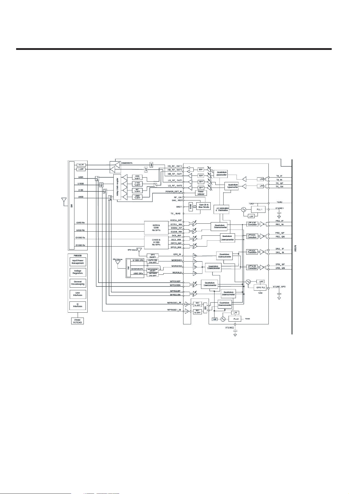
Fig 1.1 Block diagram of RF part

LGE Internal Use Only
Copyright © 2008 LG Electronics. Inc. All right reserved.
Only for training and service purposes
A generic, high-level functional block diagram of CB630 is shown in Figure 1.1. One antenna collects
base station forward link signals and radiates handset reverse link signals. The antenna connects with
receive and transmit paths through a FEM(Front End Module) (plus two duplexers for UMTS high-band
and low-band operations).
CB630 power supply voltages are managed and regulated by the PM6658 Power Management IC.
This versatile device integrates all wireless handset power management, general housekeeping, and
user interface support functions into a single mixed signal IC. It monitors and controls the external
power source and coordinates battery recharging while maintaining the handset supply voltages using
low dropout, programmable regulators.
The device’s general housekeeping functions include an ADC and analog multiplexer circuit for
monitoring on-chip voltage sources, charging status, and current flow, as well as userdefined off-chip
variables such as temperature, RF output power, and battery ID. Various oscillator, clock, and counter
circuits support IC and higher-level handset functions. Key parameters such as under-voltage lockout
and crystal oscillator signal presence are monitored to protect against detrimental conditions.
3.1.1 Primary receive signal paths
The RTR6285/6280 receive paths include four GSM/EDGE Rx signal paths that support GSM 850,
GSM 900, GSM 1800, and GSM 1900 bands and four WCDMA Rx signal paths (two single-ended and
two differential) for one UMTS low-band and three UMTS high bands.
The quad-band GSM/EDGE Rx paths start from the handset front-end circuits (GSM Rx filters and
antenna switch module). The four differential inputs are amplified with gain-stepped LNA circuits. Gain
control is provided through software and serial interface. The LNA outputs drive the RF ports of
quadrature RF-to-baseband downconverters. The downconverted baseband outputs are multiplexed
and routed to lowpass filters (one I and one Q) whose passband and stopband characteristics
supplement MSM device processing. These filter circuits allow DC offset corrections, and their
differential outputs are buffered to interface with the MSM IC.
The two RTR6285/6280 UMTS single-ended inputs accept UMTS 2100/1900/1800/1700 input signals
from the handset RF front-end filters. The UMTS Rx inputs are provided with on-chip LNAs that
amplify the signal before second-stage filters that provide differential signals to a shared
downconverter. This second-stage input is configured differentially to optimize second-order
intermodulation and common mode rejection performance. The gain of the UMTS front-end amplifier
and the UMTS second-stage differential amplifier is adjustable, under MSM control, to extend the
dynamic range of the receivers.
The second-stage UMTS Rx amplifiers drive the RF ports of the quadrature RF-to-baseband
downconverters. The downconverted UMTS Rx baseband outputs are routed to lowpass filters having
passband and stopband characteristics suitable for UMTS Rx processing. These filter circuits allow DC
offset corrections, and their differential outputs are buffered to an interface shared with GSM Rx to the
MSM IC. The UMTS baseband outputs are turned off when the RTR6285/6280 is downconverting
GSM signals and turned on when the UMTS is operating.
The RTR6285/6280 UMTS differential input paths stay on-chip; off-chip interstage filtering is not
required. Other than this, the architecture is similar to the single-ended inputs.
3. TECHNICAL BRIEF
- 20 -

LGE Internal Use Only
Copyright © 2008 LG Electronics. Inc. All right reserved.
Only for training and service purposes
3. TECHNICAL BRIEF
- 21 -
3.1.2 Transmit signal paths
The RTR6285/6280 transmit includes four transmit signal paths (two high bands and two low bands)
supporting multi-bands and multi-modes GSM/GPRS/EDGE polar transmit and WCDMA/HSDPA
transmit architectures.
The transmit path begins with differential baseband signals (I and Q) from the MSM device. These
analog input signals are buffered, filtered by low-path filter, corrected for DC offsets, amplified, and
then applied to the quadrature upconverter mixers.
The upconverter outputs are amplified by multiple variable gain stages that provide transmit AGC
control. SSBI is used to do the gain control. The specified driver amplifier output level is achieved
while supporting the GSM/EDGE and UMTS transmit standard’s requirements for GSM ORFS, carrier
and image suppression, WCDMA ACLR, spurious emissions, Rx-band noise, and so forth.
These upconverters translate the polar GMSK-modulated or 8-PSK modulated baseband PM signals
and/or WCDMA baseband signals directly to the RF signals, which are filtered and feed into the
GSM/EDGE polar PA and/or WCDMA PA. The WCDMA TX power is coupled back to the
RTR6285/6280 internal power detector input pin, PWD_DET_IN, using a coupler for power
measurement.
The low-band drive amplifiers are used to transmit the polar phase modulated (PM) signal for
GSM/EDGE 850/900 while the high-band driver amplifiers are for the GSM/EDGE 1800/1900. By
using the radioOne architecture, the same high-band transmit path can be used to transmit the UMTS
2100/1900/1800/1700 signal, and the low-band transmit path can be used to transmit the UMTS
800/850/900 signal, depending on the application.
The envelope path is used in polar mode of operation for GSM and EDGE. Input from the MSM IC, the
baseband envelope (AM) current signal is applied directly to the ramp control pin of the GSM/EDGE
polar PA to modulate the power supply of the PA so that the polar-modulated GSM/EDGE signal in the
MSM device can be recovered and transmitted.

LGE Internal Use Only
Copyright © 2008 LG Electronics. Inc. All right reserved.
Only for training and service purposes
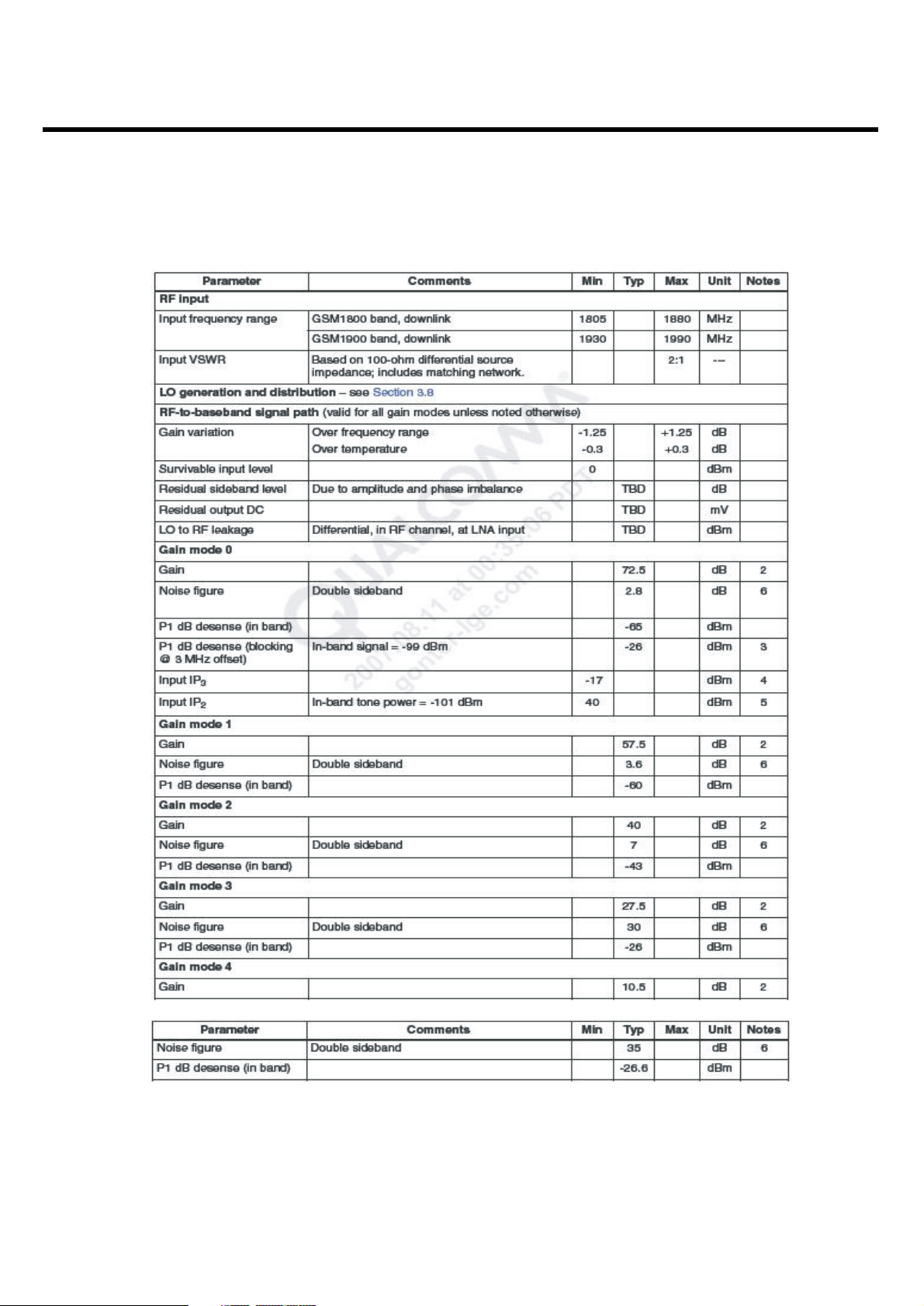
3.2 GSM/EDGE receive specifications
The RTR6285/6280 IC includes four receive signal paths: GSM 850, GSM 900, GSM 1800, and GSM
1900. Specifications for all paths are presented in the following sections.
3.2.1 GSM 850/900 receive signal path
The GSM 850 and GSM 900 receive signal path specifications in this subsection are based on the test
input described in the notes following Table 1.2-1. This test input allows measurements using standard
50-ohm single-ended test equipment even though the RTR6285/6280 IC requires a differential signal
at the GSM 850 input (pins 30 and 31). Handset implementations are expected to accomplish this
singleended to differential transformation using a SAW filter; the filter, matching components; and PCB
traces must provide adequate amplitude and phase balance (≤1 dB and ≤5 degrees, respectively).
3. TECHNICAL BRIEF
- 22 -

LGE Internal Use Only
Copyright © 2008 LG Electronics. Inc. All right reserved.
Only for training and service purposes
3. TECHNICAL BRIEF
- 23 -
Table 1.2-1 GSM 850/900 receive signal path specifications
LGE Internal Use Only
Copyright © 2008 LG Electronics. Inc. All right reserved.
Only for training and service purposes
Notes:
1. The analog baseband output pins from RTR6285/6280 are connected to the MSM ICs. Individual
trace and load capacitance should not to exceed 15 pF on the I or Q lines to the MSM. The I and Q
load resistance and capacitance should be equal.
2. Gain values account for unit conversion from the total input power (dBm) to the output voltage
(dBVRMS) of one component (I or Q).
3. Out-of-band jammer (blocker) input power that reduces the in-band output signal power by 1 dB.
4. Test conditions for third-order input intercept point measurements: CW input jammer level = -49 dBm
at 800 kHz offset, CW input jammer level = -49 dBm at 1650 kHz offset.
5. Test conditions for in-band second-order input intercept point measurements: CW input jammer #1
level = -33 dBm at 6000 kHz offset, CW input jammer #2 level = -33 dBm at 6050 kHz offset.
6. Noise figure must be met for 2:1 source VSWR in a 100-ohm system. Noise figure or output noise
voltage is integrated from 100 Hz to 100 kHz.
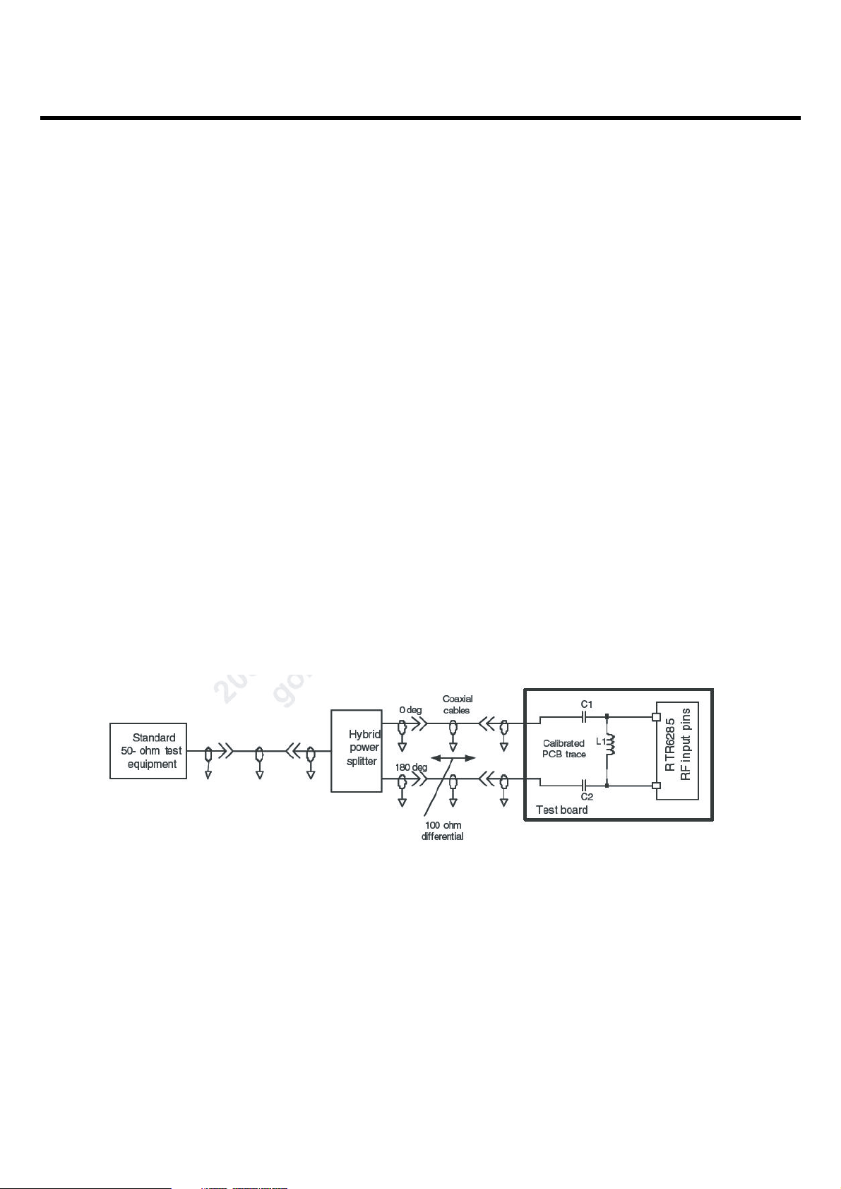
7. Performance specifications are based on measurements taken using a hybrid power splitter to create
two 50-ohm outputs that are 180 degrees out-of-phase (Figure 1.2-1). The result is a 100-ohm
differential input to the test board connected by two coaxial cables, with calibrated traces to the
RTR6285/6280 input and its matching components. The matching circuit for IClevel testing is
different than recommended handset designs. See the RTR6285/6280 Device User Guide for
recommendations. Performance specifications listed in the table include the matching networks but
not the hybrid splitter, coaxial cables, or calibrated PCB traces.
3.2.2 GSM 1800/1900 receive signal path
The GSM1800 receive signal path specifications given in this subsection are based on the test input
described in the Table 1.2-2 notes. This test input allows measurements using standard 50-ohm
singleended test equipment even though the RTR6285/6280 IC requires a differential signal at the GSM
1800 input (pins 36 and 37). Handset implementations are expected to accomplish this single-ended to
differential transformation using a SAW filter; the filter, matching components, and PCB traces must
provide adequate amplitude and phase balance (≤1.5 dB and ≤15 degrees, respectively).
3. TECHNICAL BRIEF
- 24 -
Figure 1.2-1
LGE Internal Use Only
Copyright © 2008 LG Electronics. Inc. All right reserved.
Only for training and service purposes
3. TECHNICAL BRIEF
- 25 -
Table 1.2-2 GSM 1800/1900 receive signal path specifications
LGE Internal Use Only
Copyright © 2008 LG Electronics. Inc. All right reserved.
Only for training and service purposes
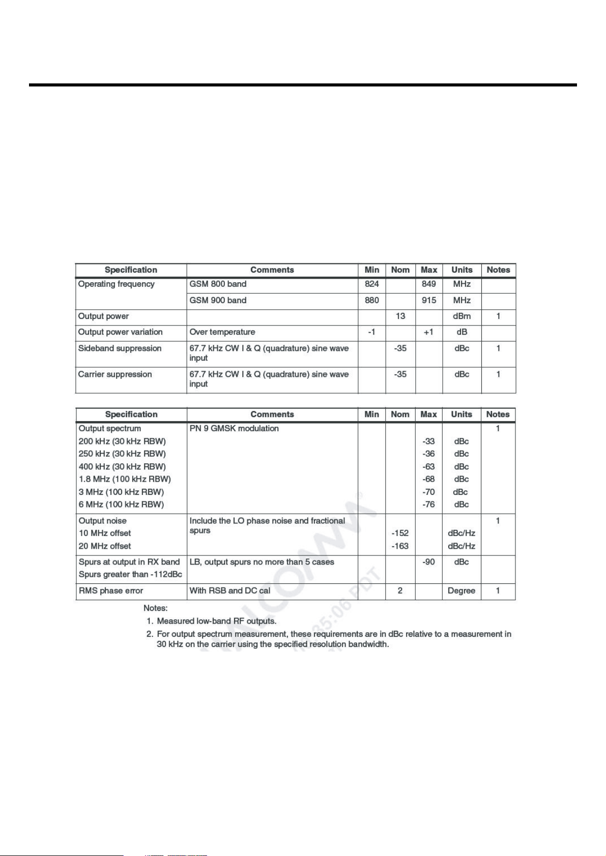
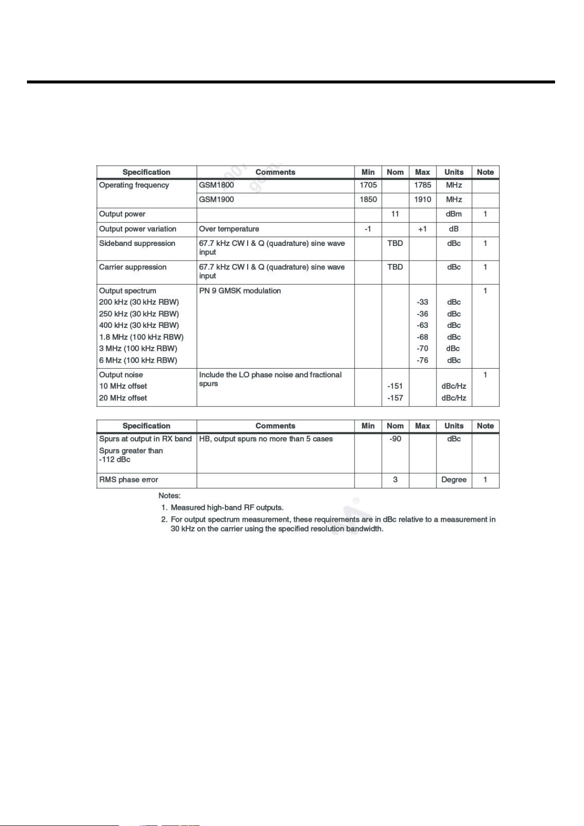
3.2.3 GSM/EDGE transmit signal path specifications
The RTR6285/6280 IC includes significant circuits for supporting GSM/EDGE polar transmit signal
paths, which include low-band path for GSM 850 and GSM 900, and highband path for GSM 1800 and
GSM 1900. The baseband I/Q signals from MSM are directly upconverted to RF frequency using ZIF
architecture. Specifications for each set of transmitter circuits are given in the following sections.
3. TECHNICAL BRIEF
- 26 -
Table 1.2-3 GSM 850/900 transmit signal path specifications
LGE Internal Use Only
Copyright © 2008 LG Electronics. Inc. All right reserved.
Only for training and service purposes
3. TECHNICAL BRIEF
- 27 -
Table 1.2-4 GSM 1800/1900 transmit signal path specifications
LGE Internal Use Only
Copyright © 2008 LG Electronics. Inc. All right reserved.
Only for training and service purposes
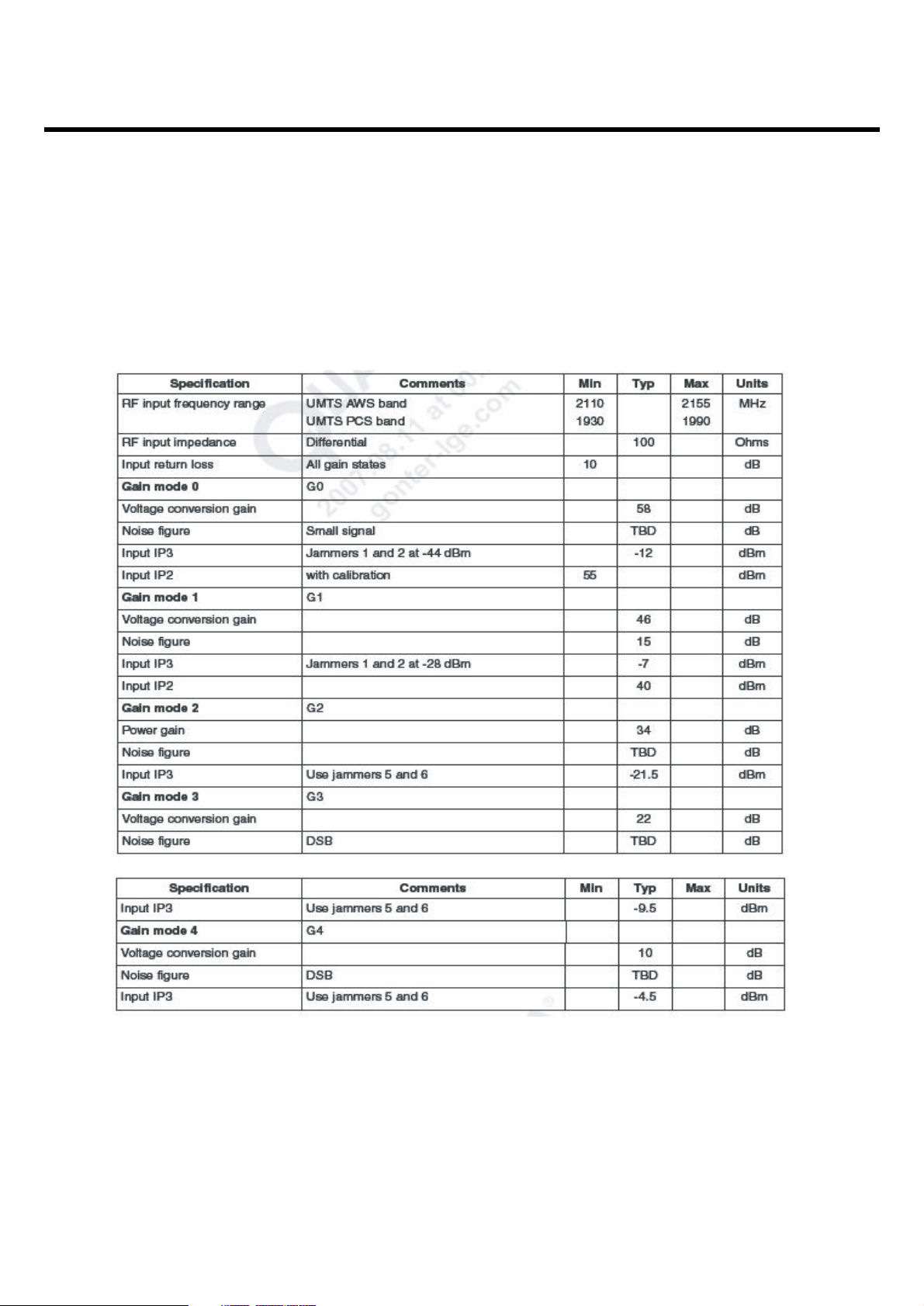
3.3 WCDMA primary receive signal path specifications
3.3.1 WCDMA balanced high-band primary receive specifications
3. TECHNICAL BRIEF
- 28 -
Table 1.3-1 WCDMA balanced high-band primary receive specifications
LGE Internal Use Only
Copyright © 2008 LG Electronics. Inc. All right reserved.
Only for training and service purposes
3. TECHNICAL BRIEF
- 29 -
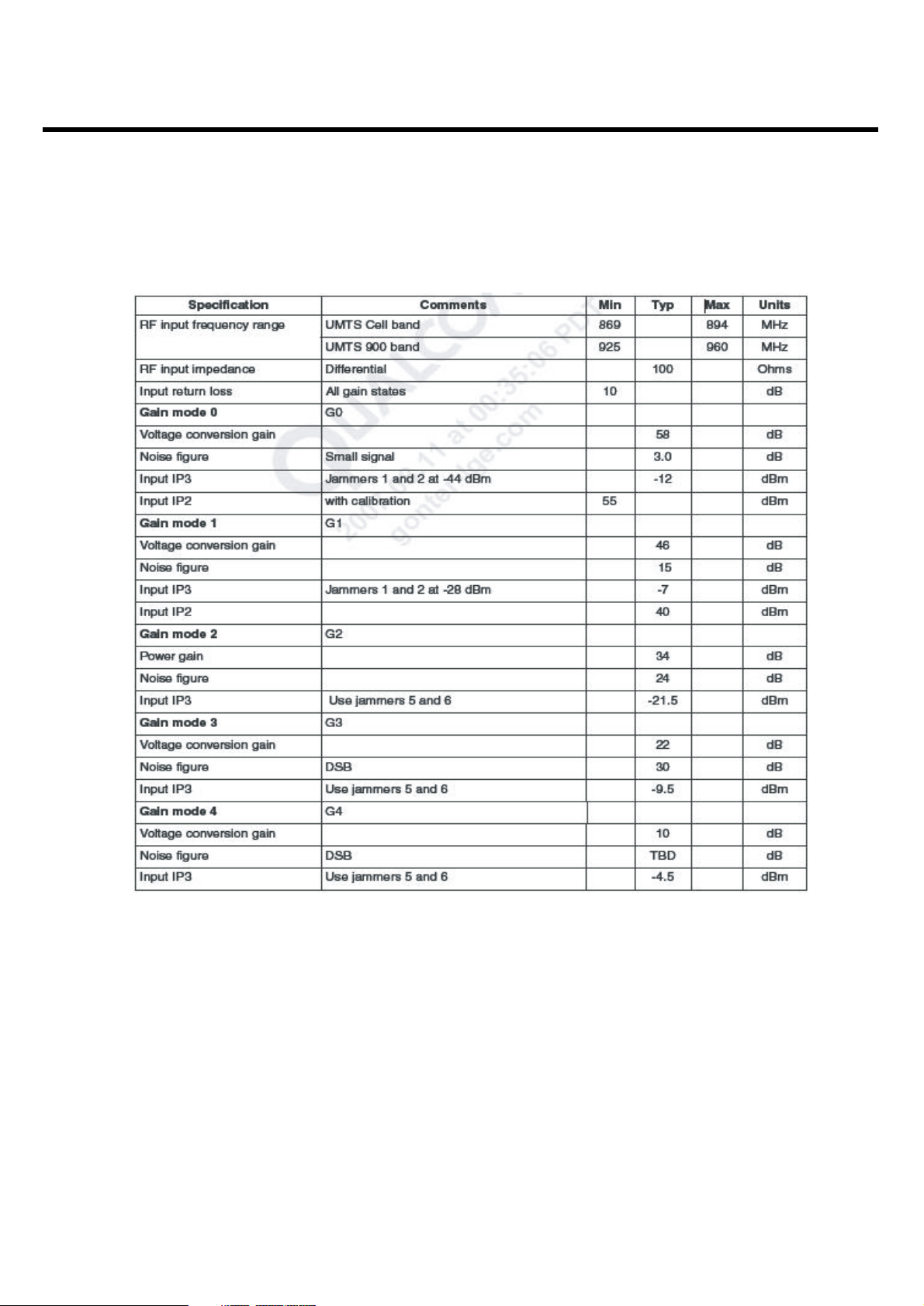
3.3.2 WCDMA balanced low-band primary receive specifications
Table 1.3-2 WCDMA balanced low-band primary receive specifications
LGE Internal Use Only
Copyright © 2008 LG Electronics. Inc. All right reserved.
Only for training and service purposes
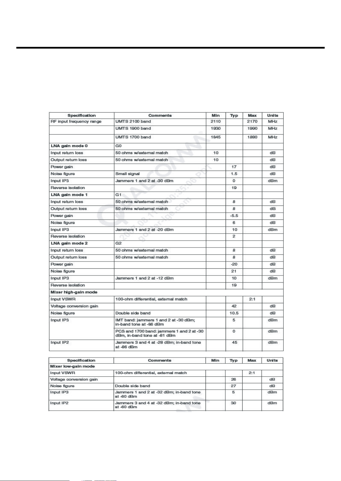
3.3.3 WCDMA unbalanced primary receive specifications (high bands only)
3. TECHNICAL BRIEF
- 30 -
Table 1.3-3 WCDMA unbalanced primary receive specifications (high bands only)
LGE Internal Use Only
Copyright © 2008 LG Electronics. Inc. All right reserved.
Only for training and service purposes
3. TECHNICAL BRIEF
- 31 -
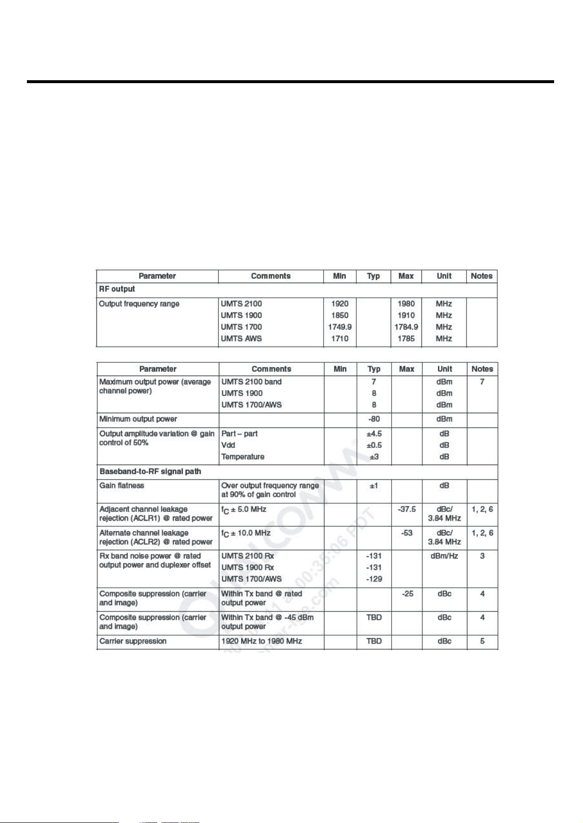
3.4 WCDMA transmit signal path specifications
The RTR6285/6280 WCDMA transmit paths share the same transmit paths as GSM and support
multitransmit modes: UMTS 2100, UMTS 1900, and UMTS 1800 on high-band transmit drivers, and
UMTS 800 and UMTS 850 on low-band transmit drivers.
3.4.1 UMTS high-band transmit signal path
Table 1.4-1 UMTS high-band Tx specifications
LGE Internal Use Only
Copyright © 2008 LG Electronics. Inc. All right reserved.
Only for training and service purposes
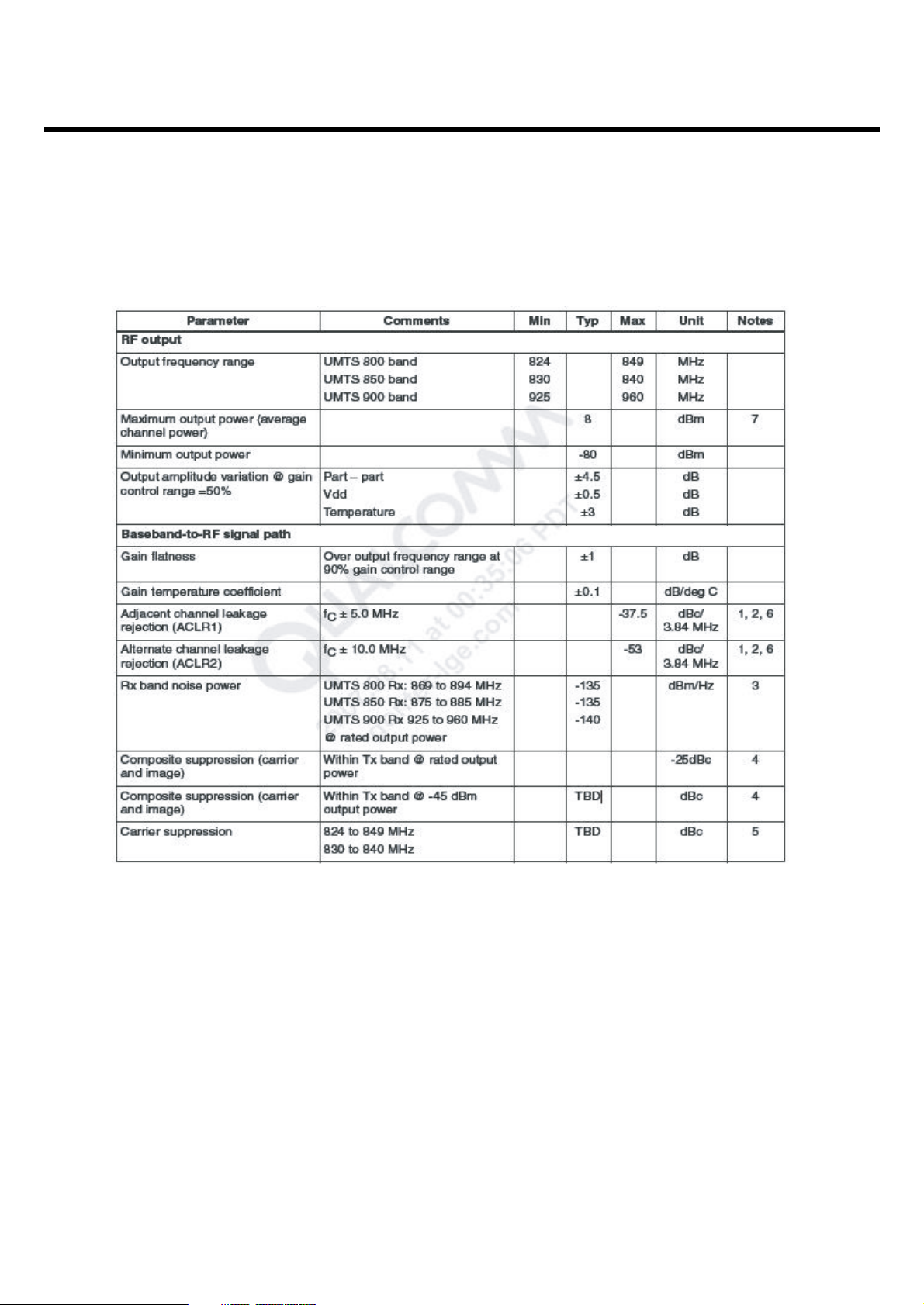
3.4.2 UMTS low-band transmit signal path
3. TECHNICAL BRIEF
- 32 -
Table 1.4-2 UMTS low-band Tx specifications

LGE Internal Use Only
Copyright © 2008 LG Electronics. Inc. All right reserved.
Only for training and service purposes
3. TECHNICAL BRIEF
- 33 -
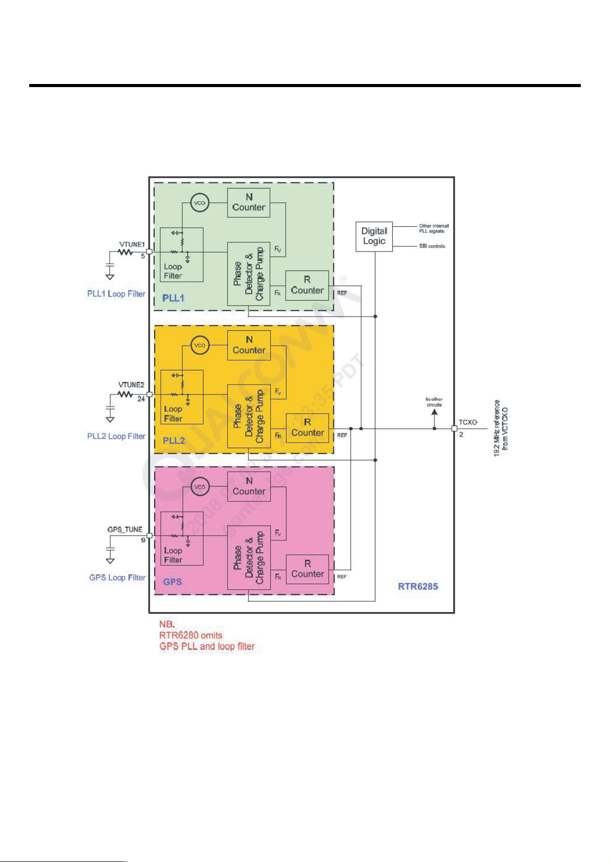
3.5 LO Phase-locked Loop
All LO functions are fully integrated on-chip and do not require any user adjustment.
Qualcomm has established and implemented frequency plans and LO generation schemes that support
the radioOne Platform F/G-series chipset. Only one area requires handset designer attention: the loop
filters relating to each PLL. These are addressed in this chapter. All the UMTS Tx/Rx, GSM Tx/Rx and
GPS PLL circuits are included within the RTR6285: reference dividers, phase detectors, charge pumps,
feedback dividers, and digital logic. The RTR6280 integrates all the same PLL circuits as the RTR6285
with the exception of GPS. There are three integrated VCOs and PLLs within the Platform F/G
(RFCMOS) chipset as shown in Figure 1.5-1:
■
PLL1 produces the LO for up-/down-conversion of GSM Tx/Rx, and UMTS Tx
■
PLL2 produces the Rx LO for the UMTS primary and diversity down-conversion
■
PLL3 produces the LO for GPS down-conversion
A buffered 19.2 MHz VCTCXO signal provides the synthesizer input (VCTCXO), the frequency
reference to which the PLL is phase- and frequency-locked. The reference is divided by the Rcounters
to create a fixed-frequency input to the phase detector, FR. The other phase detector input (FV) varies
as the loop acquires lock, and is generated by dividing the VCO frequency using the feedback path
Ncounter.
The closed loop will force FV to equal FR when locked. If the loop is not locked, the error between FV
and FR will create an error signal at the output of the charge pump. This error signal is filtered by the
loop filter components and applied to the VCO, tuning the output frequency so that the error is
decreased. Ultimately, the loop forces the error to approach zero and the PLL is phase- and frequencylocked. All of the key PLL components affecting the PLL performance - such as VCO sensitivity, charge
pump circuit current, PLL topology and loop filter (with the exception of one capacitor) - are integrated
into the RFIC. This means that proper handset performance is assured.
LGE Internal Use Only
Copyright © 2008 LG Electronics. Inc. All right reserved.
Only for training and service purposes
3. TECHNICAL BRIEF
- 34 -
Fig 1.5-1 RTR6285 PLLs functional block diagram
LGE Internal Use Only
Copyright © 2008 LG Electronics. Inc. All right reserved.
Only for training and service purposes
3. TECHNICAL BRIEF
- 35 -
3.6 Off-chip RF Components
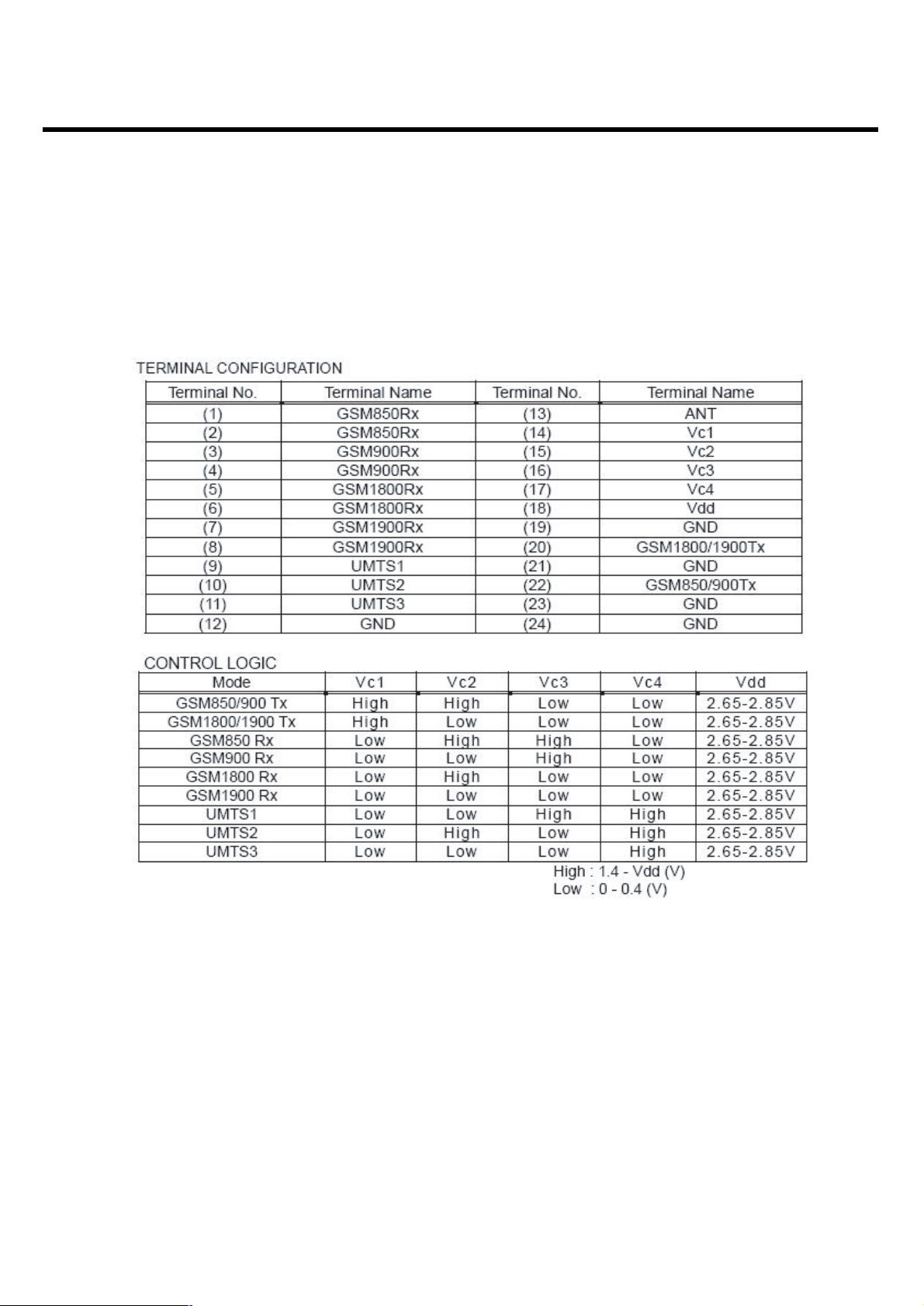
3.6.1 Antenna Switch Module
Table 1.6-1 Terminal configuration and Control logic

- 36 -
3. TECHNICAL BRIEF
3.6.2 UMTS duplexer
A UMTS duplexer splits a single operating band into receive and transmit paths. Important performance
requirements include;
Insertion loss . this component is also in the receive and transmit paths ;
In the CB630 typical losses : UMTS1900_ Tx = 2.1 dB, UMTS1900_ Rx = 2.8 dB and UMTS850_
Tx =1.9 dB, UMTS850_ Rx = 2.7 dB
Out-of-band rejection or attenuation. The duplexer provides input selectivity for the receiver, output
filtering for the transmitter, and isolation between the two. Rejection levels for both paths are specified
over a number of frequency ranges. Two Tx-to-Rx isolation levels are critical to receiver performance:
Rx-band isolation. The transmitter is specified for out-of-band noise falling into the Rx band. This noise
leaks from the transmit path into the receive path, and must be limited to avoid degrading receiver
sensitivity. The required Rx-band isolation depends on the PA out of-band noise levels and Rx-band
losses between the PA and LNA. Minimum duplexer Rx band isolation value is about 45 dB.
Tx-band isolation. The transmit channel power also leaks into the receiver. In this case, the leakage is
outside the receiver passband but at a relatively high level. It combines with Rx band jammers to create
cross-modulation products that fall in-band to desensitize the receiver. The required Tx-band isolation
depends on the PA channel power and Tx-band losses between the PA and LNA. Minimum duplexer
Tx-band isolation value is about 55 dB.
Passband ripple. The loss of this fairly narrowband device is not flat across its passband. Passband
ripple increases the receive or transmit insertion loss at specific frequencies, creating performance
variations across the band.s channels, and should be controlled.
Return loss. Minimize mismatch losses with typical return losses of 10 dB or more (VSWR <2:1).
Power handling. High power levels in the transmit path must be accommodated without degraded
performance. The specified level depends on the operating band class and mobile station class (per the
applicable standard), as well as circuit losses and antenna EIRP. Several duplexer characteristics
depend upon its source and load impedances. QUALCOMM strongly recommends an isolator be used
between the UMTS PA and duplexer to assure proper performance.
LGE Internal Use Only
Copyright © 2008 LG Electronics. Inc. All right reserved.
Only for training and service purposes
- 37 -
3. TECHNICAL BRIEF
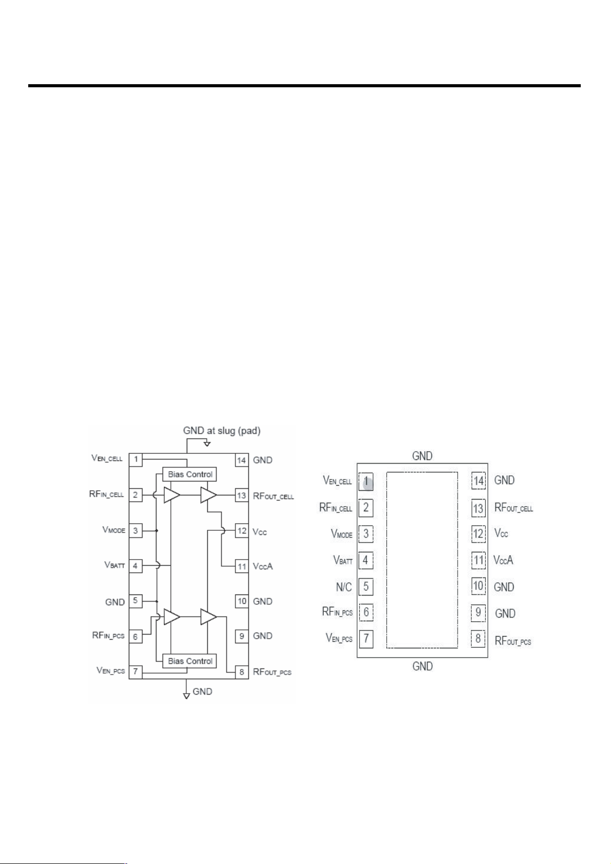
3.6.3 UMTS Power Amplifier
The AWT6321 addresses the demand for increased integration in dual-band handsets for North
American CDMA network deployments. The small footprint 3 mm x 5 mm x 1 mm surface mount RoHS
compliant package contains independent RF PA paths to ensure optimal performance in both frequency
bands, while achieving a 25% PCB space savings compared with solutions requiring two single-band
PAs. The package pinout was chosen to enable handset manufacturers to easily route VCC to both
power amplifiers and simplify control with a common VMODE pin. The device is manufactured on an
advanced InGaP HBT MMIC technology offering state-of-the-art reliability, temperature stability, and
ruggedness. The AWT6321 is part of ANADIGICS’ high-Efficiency-at-Low-Power (HELP™) family of
CDMA power amplifiers, which deliver low quiescent currents and significantly greater efficiency without
a costly external DAC or DC-DC converter. Through selectable bias modes, the AWT6321 achieves
optimal efficiency across different output power levels, specifically at low- and mid-range power levels
where the PA typically operates, thereby dramatically increasing handset talktime and standby-time. Its
built-in voltage regulator eliminates the need for external switches. The 3 mm x 5 mm x 1 mm surface
mount package incorporates matching networks optimized for output power, efficiency and linearity in a
50 Ω system.
LGE Internal Use Only
Copyright © 2008 LG Electronics. Inc. All right reserved.
Only for training and service purposes
Block Diagram Pinout
- 38 -
3. TECHNICAL BRIEF
LGE Internal Use Only
Copyright © 2008 LG Electronics. Inc. All right reserved.
Only for training and service purposes
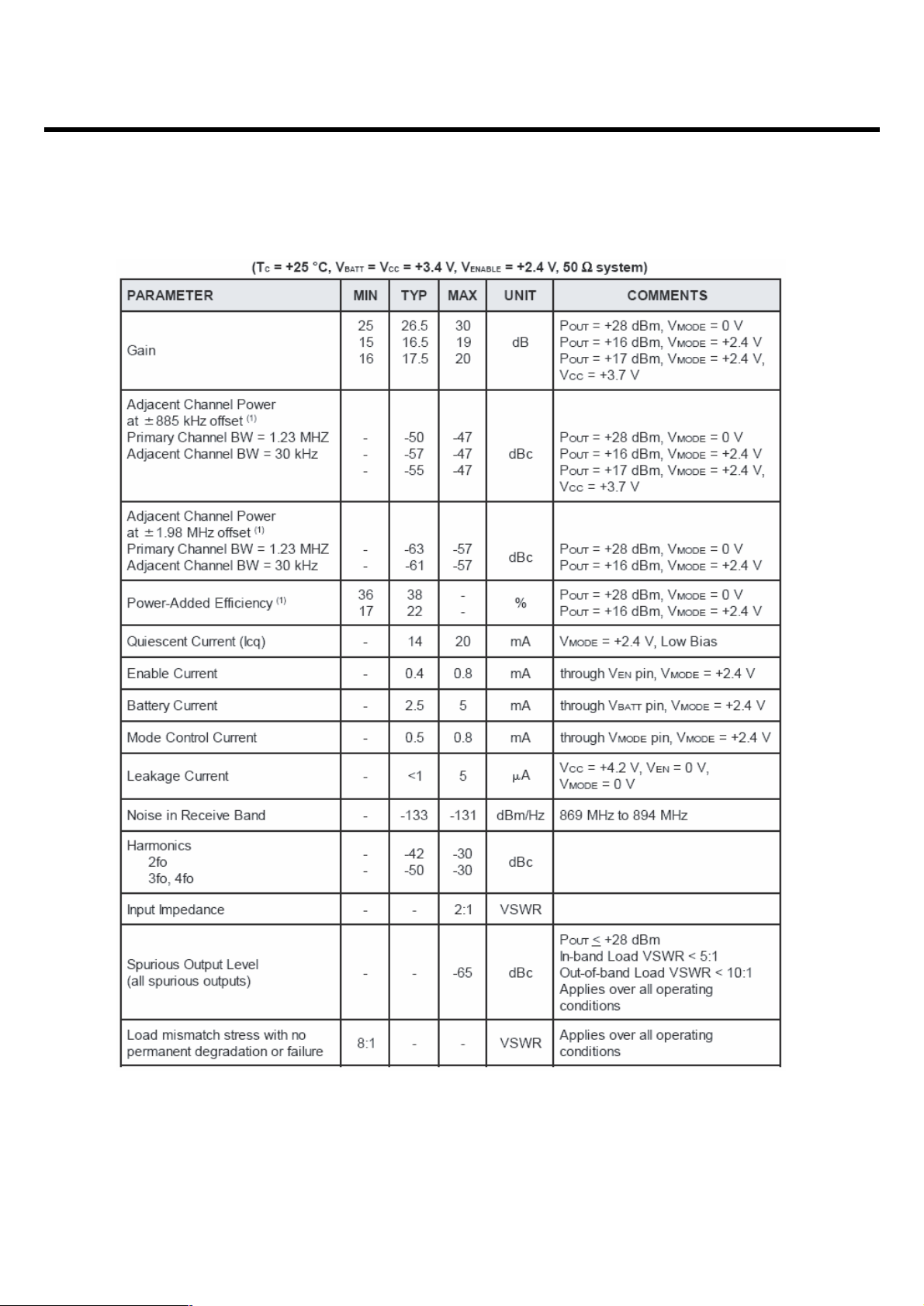
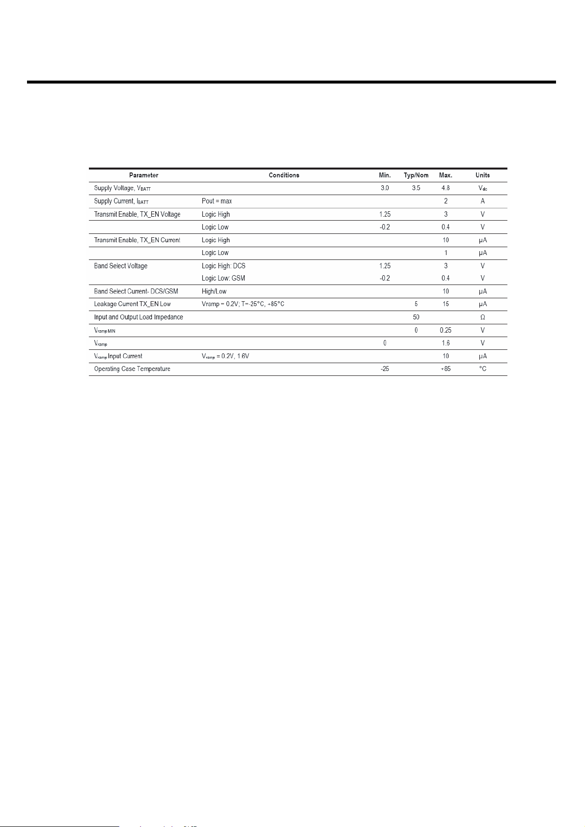
Table 1.6-3-1 Electrical specifications-Cellular Band
- 39 -
3. TECHNICAL BRIEF
LGE Internal Use Only
Copyright © 2008 LG Electronics. Inc. All right reserved.
Only for training and service purposes
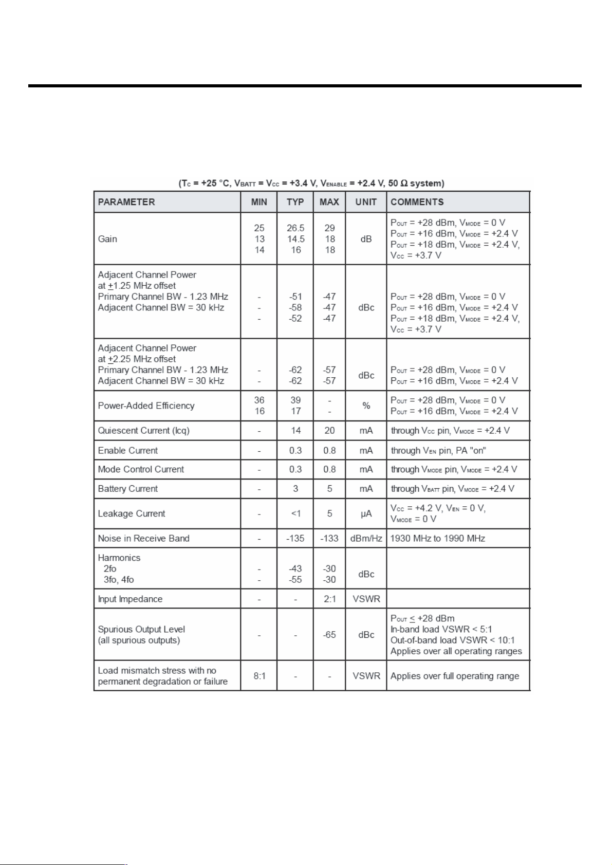
Table 1.6-3-2 Electrical specifications-PCS Band
- 40 -
3. TECHNICAL BRIEF
3.6.4 Thermistor
This thermistor senses temperature variations around UMTS PA to adjust PA gain deviation for assure
compliance with the applicable transmit power control standards. Negative temperature compensation
thermistor is used in the CB630.
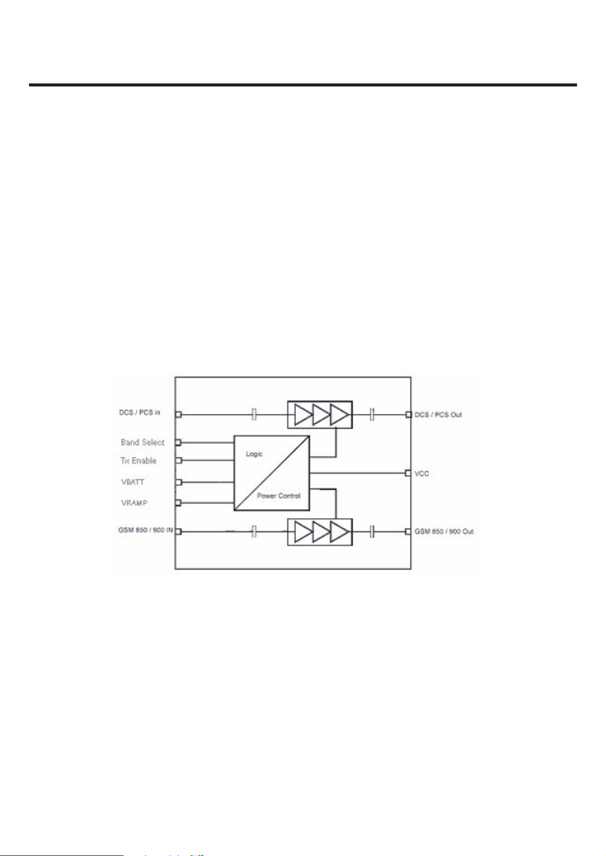
3.6.5 GSM/GPRS/EDGE Power Amplifier
Product Description
The TQM7M5012 is a ultra-small (5x5mm), GSM/EDGE Polar PAM for handset applications. This
module has been optimized for excellent EDGE efficiency, ACPR and EVM in an open loop polar
modulation environment at EDGE class E2+ operation while maintaining high GSM/GPRS efficiency.
The TQM7M5012 was optimized for operation with the Qualcomm RTR6285 regarding input power
range and Rx band performance.
LGE Internal Use Only
Copyright © 2008 LG Electronics. Inc. All right reserved.
Only for training and service purposes
Fig 1.6-5-1 GSM PA functional block diagram
- 41 -
3. TECHNICAL BRIEF
3.6.6 UMTS primary Rx RF filter
RF filters are located between the UMTS LNA and the mixer inputs for UMTS 2100, UMTS 1900, and
UMTS 1700. Insertion loss is important, but not as critical as losses before the LNA. The most important
parameters of this component include:
■
Out-of-band rejection or attenuation levels, usually specified to meet these conditions:
❍
Far out-of-band signals - Ranging from DC up to the first band of particular concern and from the
last band of particular concern to beyond three times the highest pass-band frequency.
❍
Tx-band leakage - The transmitter channel power, although attenuated by the duplexer, still
presents a cross-modulation threat in combination with Rx-band jammers. The RF filter must
provide rejection of this Tx-band leakage.
❍
Other frequencies of particular concern - Bands known to include other wireless transmitters that
may deliver significant power levels to the receiver input.
■
Phase and amplitude balance - The ZIF architecture requires well-balanced differential inputs to the
RTR6285/RTR6280. This is accomplished by the RF filter, which takes a single-ended output from the
RTR6285/RTR6280 IC, and provides differential outputs having nominal 180° phase separation.
Phase and/or amplitude imbalance degrades common-mode rejection and second-order, non-linearity
so their requirements are specified jointly.
LGE Internal Use Only
Copyright © 2008 LG Electronics. Inc. All right reserved.
Only for training and service purposes
Fig 1.6-5-2 Operating Parameter

- 42 -
3. TECHNICAL BRIEF
3.6.7 UMTS Diversity Rx RF filter
The diversity receiver path does not require a duplexer to separate Rx and Tx signals, but must include
an Rx filter before the first gain stage to achieve performance comparable to the Rx-path within a
duplexer. In the UMTS paths the first gain stage is at the RTR6285 input. Key performance
requirements of the first bandpass filter include:
■
Insertion loss - this component is positioned before the first gain stage, so its loss degrades receiver
noise figure (sensitivity) directly. Insertion loss is most critical here!
■
Out-of-band rejection or attenuation - this filter provides input selectivity for the receiver and
suppresses transmitter leakage. Rejection levels are specified over a number of frequency ranges
(see device data sheets for representative values).
❍
Tx-band leakage - the transmitter channel power combines with Rx-band jammers to create
crossmodulation within the LNA or pre-LNA that falls in-band and corrupts receiver performance.
Furthermore, the secondary UMTS chains have low operating points and might be driven into
compression if sufficient suppression is not achieved. The RF filter must provide rejection of this
Txband leakage.
❍
Other frequencies of particular concern - bands known to include other wireless transmitters that
may deliver significant power levels to the receiver input. Of course, passband ripple and return
loss are still important in all cases for the same reasons explained in the duplexer section. This Rx
input filter has a single-ended configuration at its input and output.
LGE Internal Use Only
Copyright © 2008 LG Electronics. Inc. All right reserved.
Only for training and service purposes
- 43 -
3. TECHNICAL BRIEF
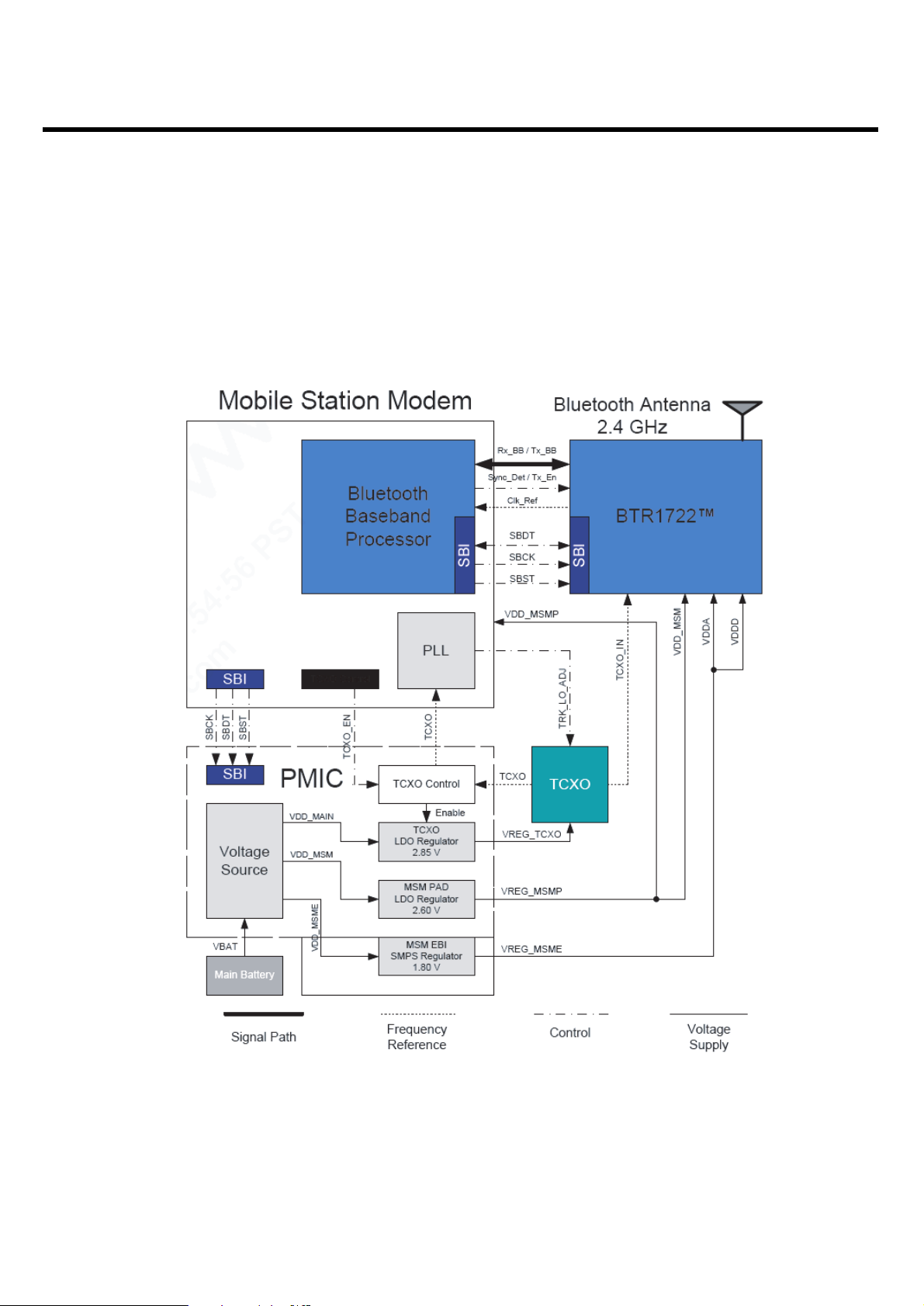
3.6.8 Bluetooth
The MSM6281 includes BT baseband embedded BT 2.0+EDR, compliant baseband core, so the other
bluetooth components are an bluetooth RF module and Antenna. Figure1.5.12-1 shows the bluetooth
system architecture in the CB630.
LGE Internal Use Only
Copyright © 2008 LG Electronics. Inc. All right reserved.
Only for training and service purposes
Fig 1.6-8 Bluetooth system architecture

- 44 -
3. TECHNICAL BRIEF
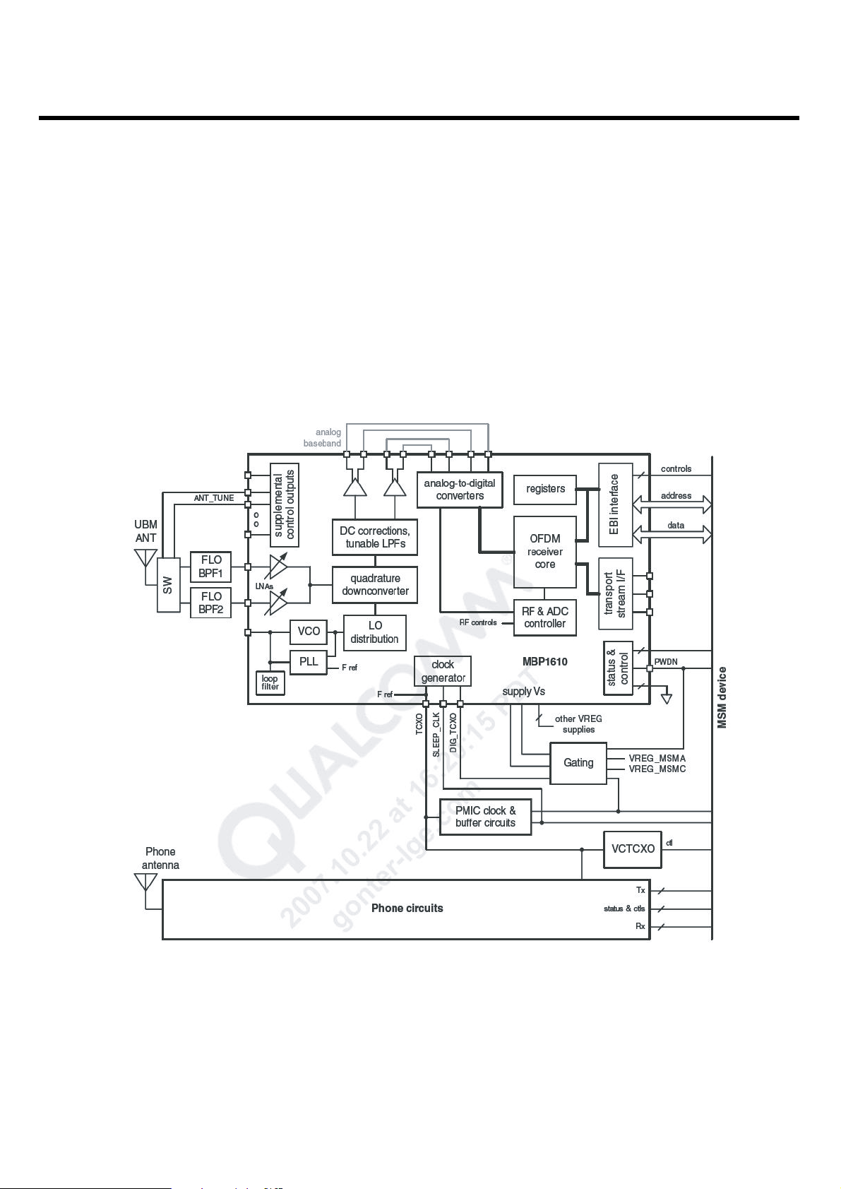
3.6.9 Media FLO
QUALCOMM Universal Broadcast Modem™ (UBM™) provides a single-chip solution for the world's
leading mobile broadcast standards. It provides handset manufacturers with unprecedented flexibility
while creating a time-to-market advantage. By combining digital and RF functionality into a single
package, the UBM chip is a size- and cost-efficient solution. QUALCOMM's UBM chipset family
includes:
■
MBP1600 - Supports wideband MediaFLO, DVB-H, and ISDB-T
■
MBP1610 - Supports MediaFLO in the United States
The MBP1610 device is a mobile broadcast platform (MBP) that simplifies the integration of
MediaFLO™ technologies into mobile wireless devices. MediaFLO is an end-to-end solution that
enables multicasting of high-quality video, audio, clipcast media, and IP data-casting to a large number
of mobile users. The forward-link only (FLO) air interface implements the physical layer of the
MediaFLO system. An overview of the MediaFLO system and FLO technology is available at
www.mediaFLO.com. Pertinent standards include:
■
TIA-1099: Forward Link Only Air Interface Specification for Terrestrial Mobile Multimedia Multicast
■
TIA-1102: Minimum Performance Specification for Terrestrial Mobile Multimedia Multicast Forward
Link Only Devices
■
TIA-1103: Minimum Performance Specification for Terrestrial Mobile Multimedia Multicast Forward
Link Only Transmitters
FLO uses orthogonal frequency division multiplexing (OFDM), a technique that provides an efficient
physical layer for delivering common source data to multiple simultaneous users. The MBP1610 device
supports FLO demodulation in a frequency band from 698 to 746 MHz.
The MBP1610 device is a highly integrated IC that performs most of the demodulation and decoding
functions. It was developed specifically to interface with the phone’s processor, such as a compatible
MSM device. The MBP1610 device’s high level of integration simplifies handset designs while saving
DC power and board space. The MSM’s ARM configures the MBP via the external bus interface (EBI).
The EBI interface is also used for physical layer data transport from the MBP1610 device to the MSM
device. The MediaFLO software protocol stacks (including video decoding and processing) are all
handled within the MSM device. In addition to mobile TV functions, an MBP1610 handset includes all
the usual phone functions, including transmit functions. An MBP1610 handset’s functional requirements
are partitioned between chipset devices to yield a complete, optimal set of phone transceiver and MBP
receiver implementations. Overall transceiver and receiver performance depends upon the combined,
complementary performance of all chipset functions. As an example, the QUALCOMM MBP1610 formfit-accurate (FFA) design uses the following chipset:
■
MBP1610 Mobile Broadcast Platform device
■
MSM6280 90 nm Mobile Station Modem™ (MSM™) device
LGE Internal Use Only
Copyright © 2008 LG Electronics. Inc. All right reserved.
Only for training and service purposes
- 45 -
3. TECHNICAL BRIEF
■
RFR6275 RF receiver device
■
RTR6275 RF transceiver device
■
PM6650 power management device
A single or dual-band implementation is supported by the MBP1610 IC. A dual-band example is shown
in Figure 1.6-9 and discussed throughout this section. A single-band implementation eliminates the RF
switch; uses only one FLO bandpass filter and only one MBP1610 low noise amplifier (LNA) input.
The second (unused) LNA input would be left open or connected to RF ground.
LGE Internal Use Only
Copyright © 2008 LG Electronics. Inc. All right reserved.
Only for training and service purposes
Fig 1.6-9 RF functional block diagram

- 46 -
3. TECHNICAL BRIEF
3.7 Digital Baseband(DBB/MSM6281)
3.7.1 General Description
A. Features(MSM6281)
• Support for multimode operation - HSDPA, Tri-band WCDMA(UMTS), quad-band
GSM/GPRS/EDGE, GPS
• The ARM926EJ-C microprocessor can operate at up to 270 MHz with variable rate, software
controlled clocks to provide greater standby time.
• Supports low-power, low-frequency crystal to enable TCXO shutoff
• Integrated USIM Controller for direct interface to USIM card
• Software-controlled power management feature
• Integrated Bluetooth 1.2 baseband processor for wireless connectivity to peripherals
• Direct interface to digital camera module with video front end image processing
• Vocoder support (AMR,FR,EFR,HR)
• Advanced 409-ball CSP packaging
• HSDPA Features
- supports release 5 December 2004 standard for HSDPA
• WCDMA Features
- supports release 99 June 2004 of the W-CDMA FDD standard
- PS data rates supporting 384kbps DL / 384kbps UL
- CS data rates supporting 64kbps DL / 64kbps UL
- AMR (all rates)
• GSM Features
- Voice features (FR,EFR,AMR,HR)
- Circuit-switched data features(9.6K,14.4K,Fax)
• GPRS Features
- Class B operation
- Multi-slot class 10 data services
- CS schemes CS1,CS2,CS3,CS4
3. BB Technical Description
LGE Internal Use Only
Copyright © 2008 LG Electronics. Inc. All right reserved.
Only for training and service purposes

- 47 -
3. TECHNICAL BRIEF
• EDGE Features
- EDGE E2 power class for 8PSK
- Class B, multi-slot class 10
- Downlink/Uplink coding schemes (CS1-4, MCS1-9)
• Operation and Services
- LCD & Camera Interface
- USIM Interface
- Dual Memory Buses(EBI1-SDRAM & EBI2-NAND Flash)
- External Memory Interface (T-Flash)
- RTC
• Data Communication
- UART (Universal asynchronous receiver transmitter)
- USB On-the-Go core supports both slave and host functionality
3. BB Technical Description
LGE Internal Use Only
Copyright © 2008 LG Electronics. Inc. All right reserved.
Only for training and service purposes
LGE Internal Use Only
Copyright © 2008 LG Electronics. Inc. All right reserved.
Only for training and service purposes
3. TECHNICAL BRIEF
- 48 -
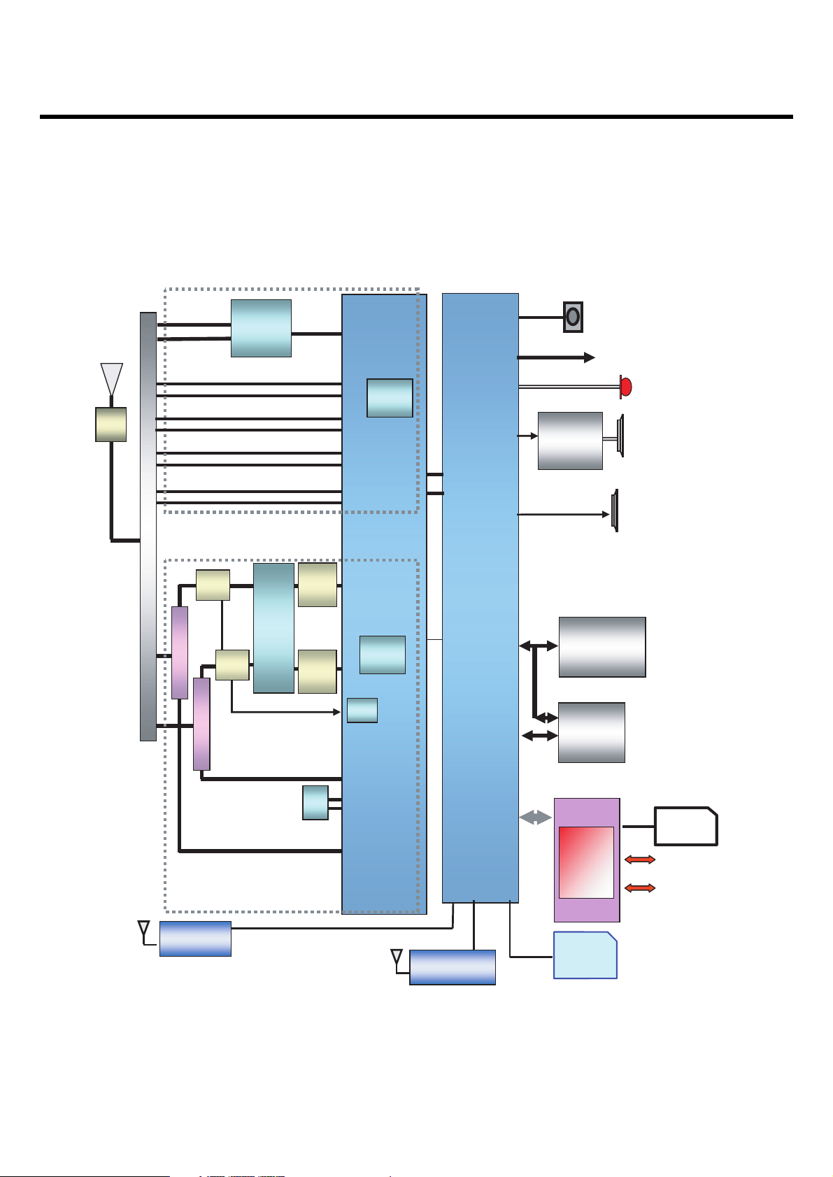
3.8 Hardware Architecture
Figure. Simplified Block Diagram
GSM
Tx/Rx
SPDT
)WAS_XR_MSG + rexelPWS( MEF
1800/1900
850/900
850
Coupler
1900
rexelpuD
rexelpuD
GSM
PA M
GSM 850 Rx
GSM 900 Rx
GSM 1800 Rx
GSM 1900
WCDMA
WCDMA
Coupler
Tx/Rx
PA
Rx
TX_SAW
M
TX_SAW
1900
GSM-VCO
RTR6285
W-VCO
HDET
I/
Q
MSM6281
S
S
B
D
T
TPA6205A
(ì2 262K, TFT)
NAND 2G
SDRAM
1G
1.3M AF camera
Stereo Headset
MIC
SPEAKER
RECEIVER
LCD
Bluetooth
LNA
850
MBP1610
Power
USIM
PM66
USB
58
+5V
T-
Micro SD
 Loading...