

Page 1

LG
Service Manual
C570
Page 2

Table Of Contents
1. INTRODUCTION................................…4
1.1 Purpose ..........................................….
1.2 Regulatory Information ......................
4
4
2. PERFORMANCE ..............................….6
2.1 H/W Feature ...................................…..
2.2 Technical Specification ...................... 68
3. TECHNICAL BRIEF ............................14
3.1 Transceiver (RTR6285, FU1)..........…..
3.2 Power Amplifier Module ................….
3.3 BT/WiFi (BCM4325, FU1 on SB) ………
3.4 PMIC (PM7540, U7)……………………….
3.5 Input power management…............….
3.6 MSM7227 (U1) .…………………………
3.7 MCP memory ......................…………….
3.8 LG display LCM ..............……………….
3.9 VGA CCM .....................…………………
3.10 2M CCM ........................................... .
3.11 Vibrator ......................... ………………
3.12 Optical Joystick…………………………
3.13 LCM backlight and keypad light .......
3.14 Side key and Qwerty key....................
3.15 USB PHY ……………….………………
3.16 T-Flash...................……………………
3.17 USIM..............………………………….
3.18 Receiver ………………………………..
3.19 Internal Microphone.....................…..
3.20 Speaker ………………………………..
3.21 3.5mm Ear-Mic with send/end key …
3.22 Main battery ……………………………
14
20
22
23
26
50
82
85
87
89
91
92
94
96
98
99
100
101
102
103
104
105
4. TROUBLE SHOOTING ................… 106
4.1 Hw Function Check……………………
4.2 FTM Mode in board level…….………
4.3 Wireless Trouble.............................….
4.4 WCDMA RX Trouble...........................
4.5 WCDMA TX Trouble..........................
4.6 GSM RX Trouble..........................……
4.7 GSM TX Trouble...........................…...
4.8 GPS Trouble........................................
4.9 WLAN/BT/FM Trouble........................
4.10 Power On Trouble..............................
4.11 Charging Trouble................................
4.12 LCD Trouble....................................
4.13 2M Camera Trouble.........................
4.14 VGA Camera Trouble………………
4.15 LCD backlight Trouble....................
4.16 KEYPAD Light Trouble...................
4.17 SIM Card Interface Trouble………..
4.18 T-Flash Trouble……………………..
4.19 USB Trouble ………………………..
4.20 Qwerty key Trouble………………...
4.21 Side key Trouble……………………
4.22 Vibrator Trouble…………………….
4.23 Receiver Trouble……………………
4.24 Speaker Trouble…………………….
4.25 Microphone Trouble…………………
4.26 Ear-Mic Trouble……………………...
107
108
109
113
139
157
167
180
193
204
208
211
215
219
223
226
230
233
236
240
243
248
251
256
261
264
5. DISASSEMBLY INSTRUCTION … 269
5.1 Disassembly ...............................
269
Page 3

6. BLOCK DIAGRAM …....................... 281
7. CIRCUIT DIAGRAM ......................... 282
8. ONE POINT REPAIR ………....... 308
9. EXPLODED VIEW &
REPLACEMENT PART LIST ...…. 318
9.1 Exploded View ........................
9.2 Replacement parts..................
10. SERVICE ENGINEERING TOOL..... 328
318
319
11. SERVICE ENGINEERING
OPERATIONS………………………...335
11.1 User Interface ...........................…
11.2 Initial Operations .........................
11.3 Hardware Test...............................
11.4 RF Auto Test ..……………............
11.5 RF Configuration ……..................
11.6 Miscellaneous Group ...................
335
336
338
343
347
363
10.1 Instruction................................
10.2 CSE Installation ...................…
10.3 Phone Mode .....................……
10.4 Driver Installation ....................
328
329
330
331
Page 4

1. INTRODUCTION
1.1 Purpose
This manual provides the information necessary to repair, calibration, description and download the
features of this model.
1.2 Regulatory Information
A. Security
Toll fraud, the unauthorized use of telecommunications system by an unauthorized part (for example,
persons other than your company’s employees, agents, subcontractors, or person working on your
company’s behalf) can result in substantial additional charges for your telecommunications services.
System users are responsible for the security of own system. There are may be risks of toll fraud
associated with your telecommunications system. System users are responsible for programming and
configuring the equipment to prevent unauthorized use. The manufacturer does not warrant that this
product is immune from the above case but will prevent unauthorized use of common-carrier
telecommunication service of facilities accessed through or connected to it.
The manufacturer will not be responsible for any charges that result from such unauthorized use.
B. Incidence of Harm
If a telephone company determines that the equipment provided to customer is faulty and possibly
causing harm or interruption in service to the telephone network, it should disconnect telephone service
until repair can be done. A telephone company may temporarily disconnect service as long as repair is
not done.
C. Changes in Service
A local telephone company may make changes in its communications facilities or procedure. If these
changes could reasonably be expected to affect the use of the this phone or compatibility with the network,
the telephone company is required to give advanced written notice to the user, allowing the user to take
appropriate steps to maintain telephone service.
D. Maintenance Limitations
Maintenance limitations on this model must be performed only by the manufacturer or its authorized agent.
The user may not make any changes and/or repairs expect as specifically noted in this manual. Therefore,
note that unauthorized alternations or repair may affect the regulatory status of the system and may void
any remaining warranty.
Page 5

1. INTRODUCTION
E. Notice of Radiated Emissions
This model complies with rules regarding radiation and radio frequency emission as defined by local
regulatory agencies. In accordance with these agencies, you may be required to provide information such as
the following to the end user.
F. Pictures
The pictures in this manual are for illustrative purposes only; your actual hardware may look slightly different.
G. Interference and Attenuation
Phone may interfere with sensitive laboratory equipment, medical equipment, etc.Interference from
unsuppressed engines or electric motors may cause problems.
H. Electrostatic Sensitive Devices
ATTENTION
Boards, which contain Electrostatic Sensitive Device (ESD), are indicated
by the sign. Following information is ESD handling:
• Service personnel should ground themselves by using a wrist strap when exchange system
boards.
• When repairs are made to a system board, they should spread the floor with anti-static mat
which is also grounded.
• Use a suitable, grounded soldering iron.
• Keep sensitive parts in these protective packages until these are used.
• When returning system boards or parts like EEPROM to the factory, use the protective
package as described.
Page 6

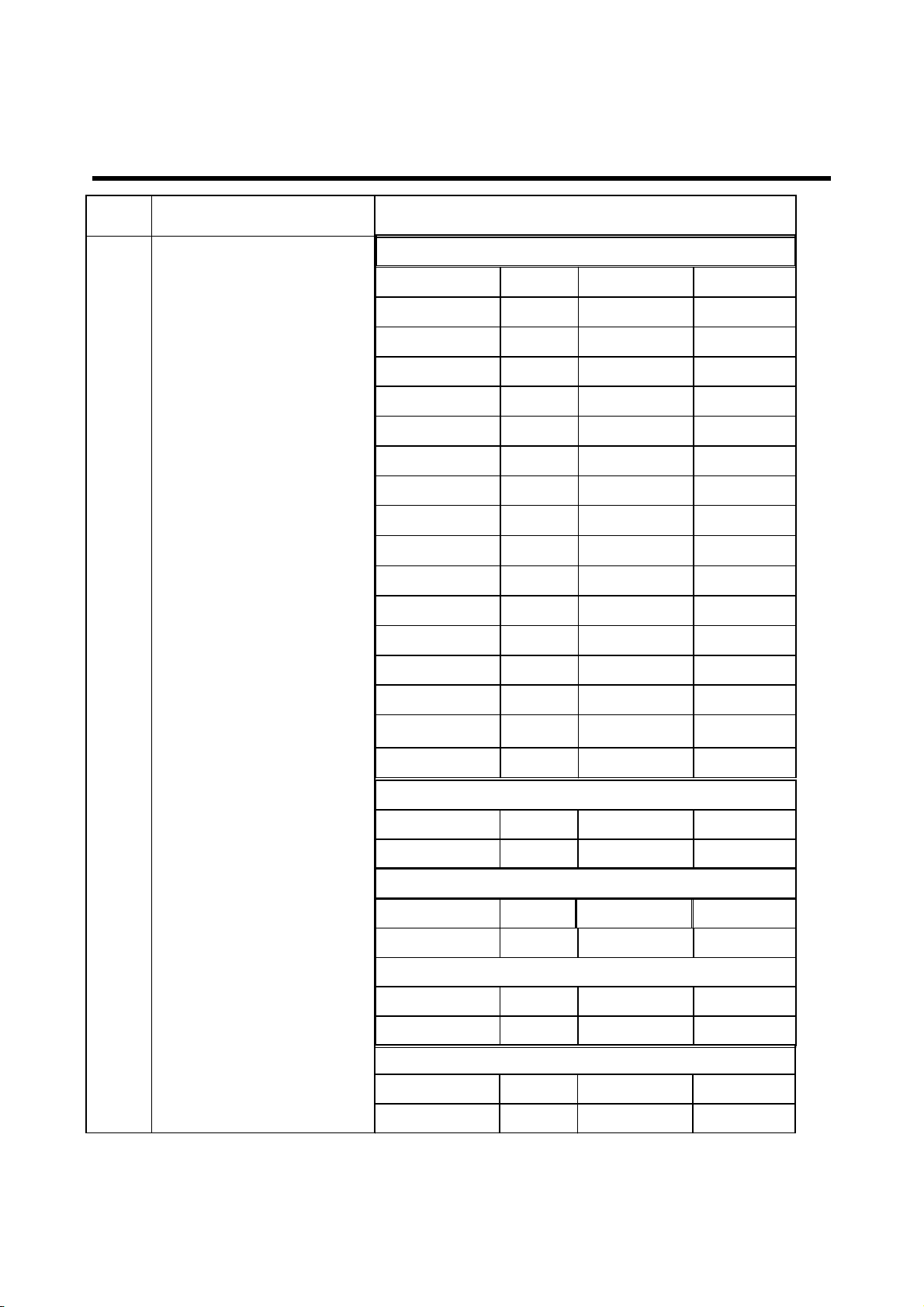
2. PERFORMANCE
2.1 H/W Features
Item Feature Comment
Standard Battery
Li-ion, 1500mAh
Battery Size : 65.3 (W) × 44(H) × 5.2(T) [mm]
Battery Weight : 31g
Standby Current
Talk time
Stand by time
Charging time Under 240 min
RX Sensitivity
TX maximum
output power
GPRS compatibility Class 12
SIM card type 3V & 1.8V
Display
Key
ANT Internal
WCDMA w/o BT: Under 3 mA (DRX=1.28)
GSM w/o BT: Under 3mA (Paging= 5 period)
WCDMA: Over 300 min (TX = 12dBm low)
GSM: Over 270min (TX= Lvl 5)
WCDMA: Over 450 hours (DRX = 1.28)
GSM: Over 450hours (Paging = 5 Period)
WCDMA: -106.7dBm/3.84MHz
GSM: -105dBm(2.439%)
WCDMA:+24dBm+1/-3 db (Power class3)/ 3.84MHz
GSM: +33dBm ± 3dB, DCS/PCS: +30dBm ± 3dB
2.4” 320 x 240 TFT LCD
Full Qwerty keypad
EAR Phone Jack Yes (stereo)
PC Synchronization Yes
Speech coding
Data and Fax
Vibrator Yes
Loud Speaker Yes
Voice Recoding Yes
Microphone Yes
EFR/FR/HR
Page 7

2. PERFORMANCE
Item Feature Comment
Speaker/Receiver Single speaker with Speaker/Receiver two mode
Travel Adapter Yes
MIDI 64 poly
MP3/AAC Yes
Options Data Cable
Page 8

2. PERFORMANCE
2.2 Technical Specification
Item Description Specification
GSM850: 824~849MHz/869~894MHz
GSM900: 880~915MHz/925~960MHz
DCS: 1710~1785MHz/1805~1880MHz
1 Frequency Band
2 Phase Error GSM: RMS : 5°, Peak : 20 °
PCS: 1850~1910MHz/1930~1990MHz
WCDMA850:824 MHz ~ 849 MHz/869~894MHz
WCDMA900 :880 MHz ~ 915 MHz/925~960MHz
WCDMA1900:1850 ~1910 MHz/1930~1990MHz
WCDMA2100:1920 MHz~1980 MHz/2110~2170MHz
3 Frequency Error
4 Power Level
GSM : 0.1 ppm
WCDMA: ±(0.1ppm+10Hz)
GSM850
Up LimitLow LimitPowerPower level
3331325
3230316
3028297
2925278
2723259
25212310
23192111
21171912
19151713
17131514
15111315
1481116
126917
104718
82519
Page 9
2. PERFORMANCE
Item
Description
Specification
DCS1800/PCS 1900
Up LimitLow LimitPowerPower level
30 28290
2927281
2725262
2622243
2420224
2218205
2016186
1814167
1612148
159129
1371010
115811
4 Power Level
93612
71413
5-1214
3-3015
WCDMA850
Up LimitLow LimitPowerPower level
252122.5 Max
WCDMA900
Up LimitLow LimitPowerPower level
252122.2Max
WCDMA1900
Up LimitLow LimitPowerPower level
252122.2 Max
WCDMA2100
Up LimitLow LimitPowerPower level
25 2122.2 Max
Page 10
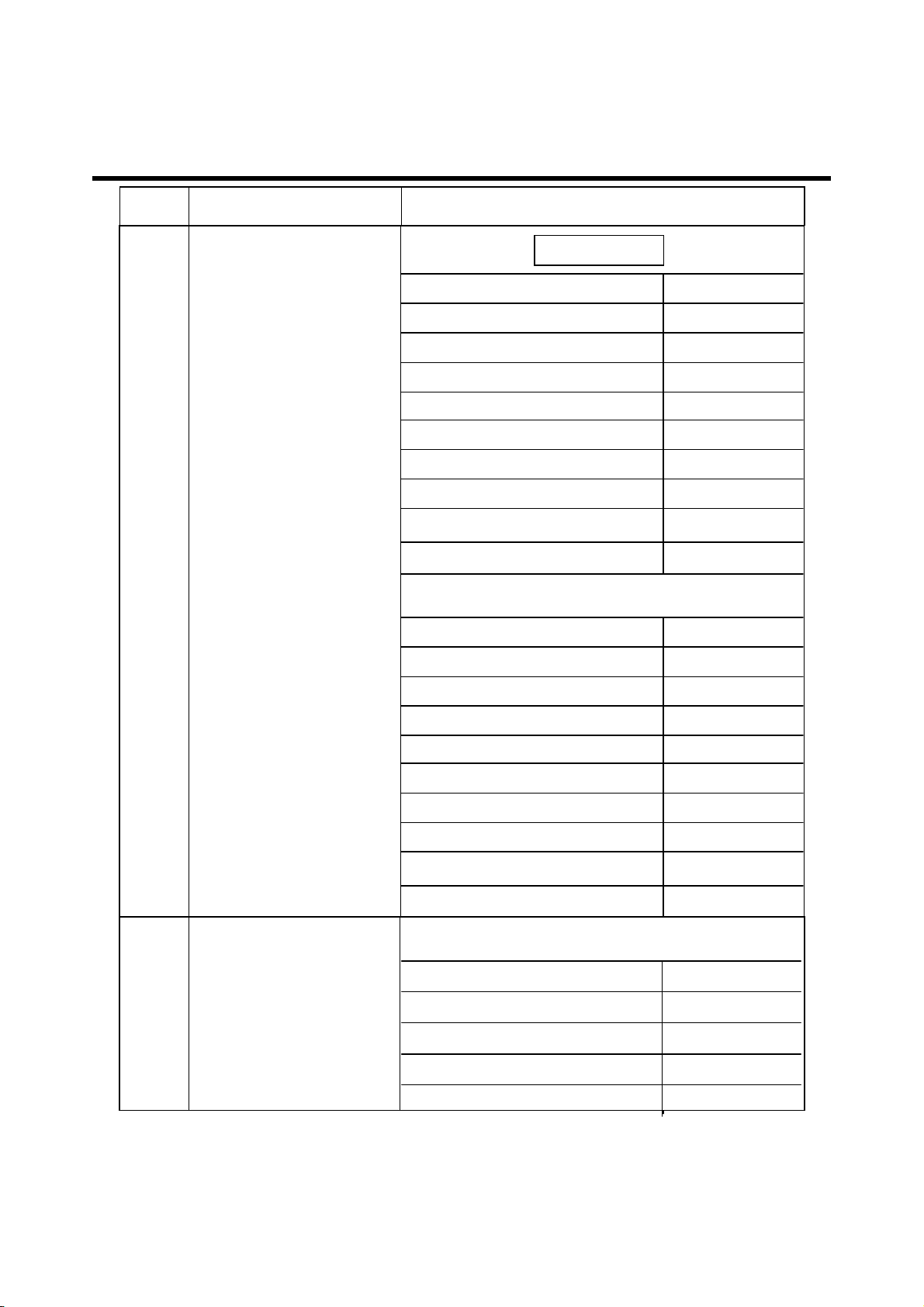
2. PERFORMANCE
Item Description Specification
GSM850 & 900
Offset from Carrier (kHz). Max. dBc
100 +0.5
200 -30
250 -33
400 -60
600~ <1,200 -60
1,200~ <1,800 -60
1,800~ <3,000 -63
3,000~ <6,000 -65
5
6
Output RF Spectrum
(due to modulation)
Output RF Spectrum
(due to switching
transient)
Offset from Carrier (kHz). Max. dBc
Offset from Carrier (kHz). Max. dBm
Offset from Carrier (kHz). Max. dBm
6,000 -71
DCS & PCS
100 +0.5
200 -30
250 -33
400 -60
600~ <1,200 -60
1,200~ <1,800 -60
1,800~ <3,000 -65
3,000~ <6,000 -65
6,000 -73
GSM900/GSM850
GSM850 & 900
400 -19
400 -19
600 -21
600 -21
1,200 -21
1,200 -21
1,800 -24
Page 11
2. PERFORMANCE
Item Description Specification
DCS & PCS
Offset from Carrier (kHz). Max. dBm
Output RF Spectrum
6
7 Spurious Emissions Conduction, Emission Status
8 Bit Error Ratio
9 RX Level Report Accuracy ±3 dB
10 SLR 14±3 dB
(due to switching
transient)
GSM850 & 900
BER (Class II) < 2.439% @-102 dBm
DCS & PCS
BER (Class II) < 2.439% @-102 dBm
WCDMA
BER < 0.1% @-106.7 dBm <REFIor>
Frequency (Hz) Max.(dB) Min.(dB)
400 -22
600 -24
1,200 -24
1,800 -27
11 Sending Response
12 RLR 3±3 dB
100 -
200 -
300 -12
1,000 -6
2,000 -6
3,000 -6
3,400 -9
4,000 -
-12
0
0
0
4
4
4
0
Page 12
2. PERFORMANCE
Item Description Specification
Frequency (Hz) Max.(dB) Min.(dB)
13 Receiving Response
* Mean that Adopt a straight line in between 300 Hz
and 1,000 Hz to be Max. level in the range.
14 STMR >17 dB
100 -
200 -
300 -7
500 -5
1,000 -5
3,000 -5
3,400 -10
4,000
-12
0
2
*
0
2
2
2
15
16 32.768KHz tolerance
17 Ringer Volume
System frequency
(13MHz tolerance)
≤ 2.5 ppm
≤30 ppm
At least 58 dB under below conditions:
1. Ringer set as ringer.
2. Test distance set as 100 cm
Page 13
2. PERFORMANCE
Item Description Specification
21 Charge Current
normal Charge : 600 mA
pre Charge : 80 mA
BAR WCDMA GSM
22 Antenna Display
BAR 4 -->
3
BAR 3 -->
2
BAR 2 -->
1
BAR 1 -->
0
-82 ±
3dBm
-92 ±
3dBm
-102 ±
3dBm
-112 ±
3dBm
23 Battery Indicator
24 Low Voltage Warning Battery Capacity < 8%
-91 ±
2dBm
-96 ±
2dBm
-101 ±
2dBm
-106 ±
2dBm
SpecificationBattery Bar
100%BAR 4 --> 3
50%BAR 3 --> 2
20%BAR 2 --> 1
8%BAR 1 --> 0
20%Low Battery Alarm
8%Critical Low Battery Alarm
0%POWER OFF
25
Forced shut down
Voltage
26 Battery Type
27 Travel Charger
3.5 ± 0.03V
1 Li-ion Battery
Standard Voltage = 3.7 V
Battery full charge voltage = 4.2 V
Capacity: 830mAh
Switching-mode charger
Input: 100 ~ 240 V, 50/60 Hz
Output: 5.1 V, 700 mA
Page 14
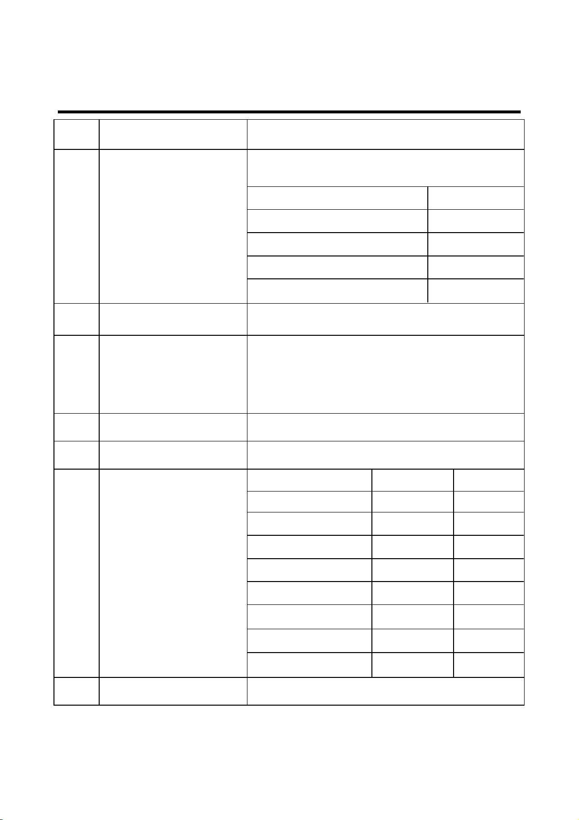
3. TECHNICAL BRIEF
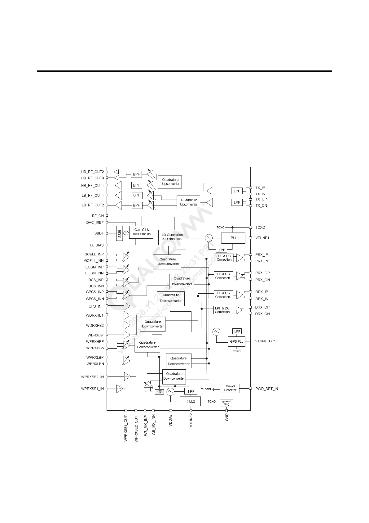
3.1 Transceiver (RTR 6285, FU1)
The RF parts consist of a transmitter part, a receiver part, a frequency synthesizer part, a voltage supply
part, and a VCTCXO part.
The RTR6285 transceiver is the integrated GSM/UMTS multi-band and multi-mode digital cellular
handsets and wireless data modems. The integrated solution also includes the GPS demodulator and the
low noise amplifier (LNAs) for UMTS and GSM RX path. The GPS LNA, RF voltage controlled oscillator
(VCO) modules, and other discrete components found in conventional designs.
Figure 3-1 RTR6285 block diagram
Page 15
3. TECHNICAL BRIEF
(1) Receiver Part
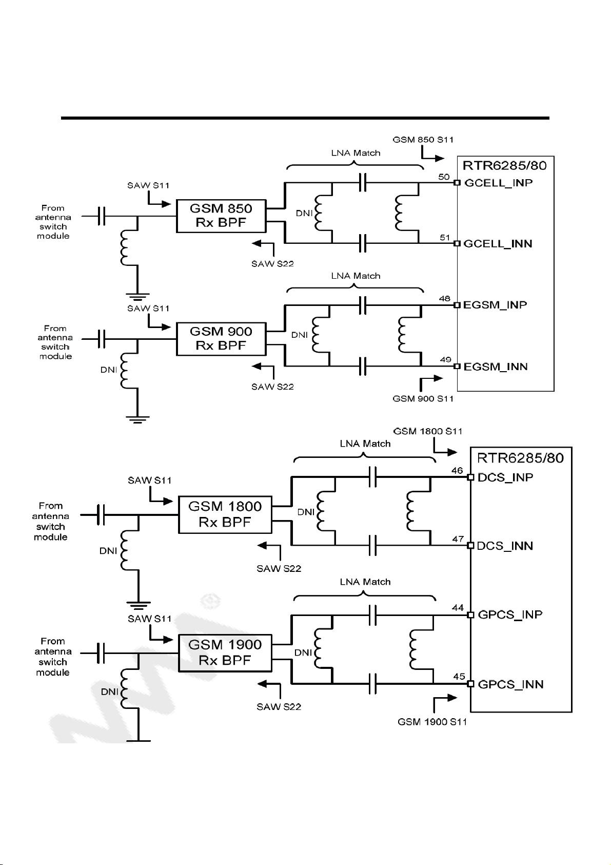
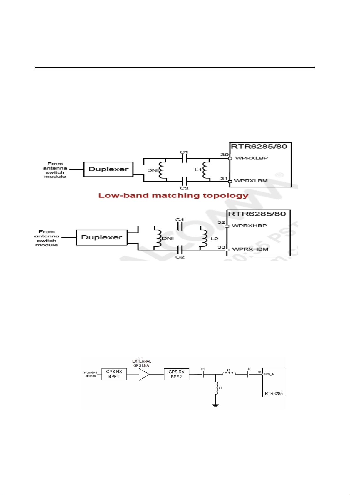
The RTR6285/RTR6280 receive paths include four GSM/EDGE Rx signal paths that support
GSM 850, GSM 900, GSM 1800, and GSM 1900 bands and four WCDMA Rxsignal paths (two
single-ended and two differential) for one UMTS low band and three UMTS high bands.
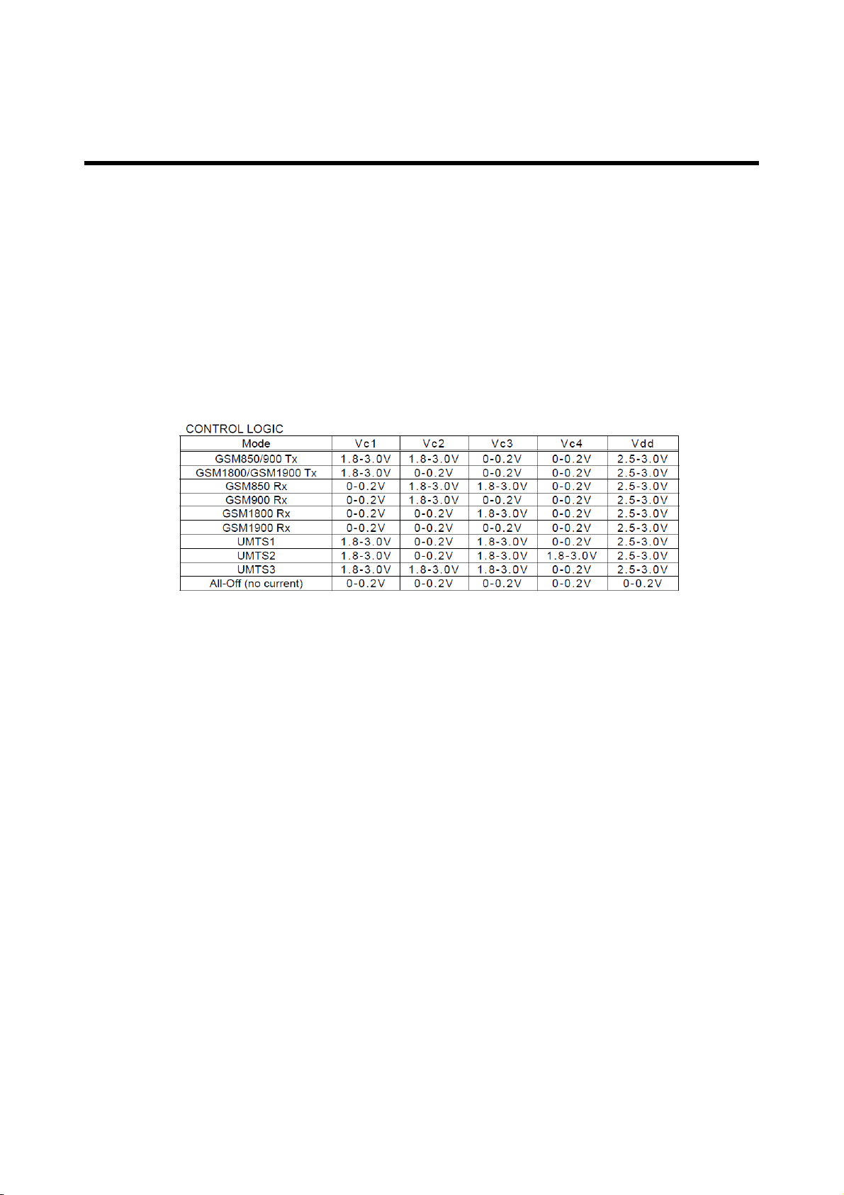
A. RF front end – Antenna Switch Module(ASM, FS1)
The quad-band GSM/EDGE Rx paths start from the handset front-end circuits (GSM Rx filters
and antenna switch module) FS1. The ASM (FS1) is used to control the Rx and Tx paths. And,
the input signals VC1, VC2, VC3 and VC4 of a FS1 are directly connected to baseband
controller to switch either Tx or Rx path on.The control logic is given below Table 3-1.
Table 3-1 THE ASM control logic
The four differential inputs are amplified with gain-stepped LNA circuits. Gain control is
provided through software and serial interface. The LNA outputs drive the RF ports of
quadrature RF-to-baseband downconverters. The downconverted baseband outputs are
multiplexed and routed to lowpass filters (one I and one Q) whose passband and stopband
characteristics supplement MSM device processing. These filter circuits allow DC offset
corrections, and their differential outputs are buffered to interface with the MSM IC. Figure 3-2
is GSM RX path from ASM to RTR6285.
Page 16
3. TECHNICAL BRIEF
Figure 3-2 THE GSM RX path
Page 17
3. TECHNICAL BRIEF
The two RTR6285/RTR6280 UMTS single-ended inputs accept UMTS 2100/1900/1800/1700
input signals from the handset RF front-end filters. The UMTS Rx inputs are provided with
on-chip LNAs that amplify the signal before second-stage filters that provide differential
signals to a shared downconverter. This second-stage input is configured differentially to
optimize second-order intermodulation and common mode rejection performance. The gain of
the UMTS front-end amplifier and the UMTS second-stage differential amplifier is adjustable,
under MSM system chip control, to extend the dynamic range of the receivers. Figure 3-3 is U
MTS RX path from ASM to RTR6285.
Figure 3-3 THE UMTS RX path
B. GPS
The GPS input path is followed by a dedicated downconverter. The GPS downconverter and
secondary WCDMA downconverter outputs are multiplexed to drive a single set of baseband
filter and buffer circuits. The secondary baseband output (in-phase and quadrature differential
signals) is routed through the DRX_I/Q pins to the MSM device for further processing. This
baseband interface supports either the WCDMA or GPS mode, whichever is active on the
secondary path.
Figure 3-4 THE GPS RX path
Page 18
3. TECHNICAL BRIEF
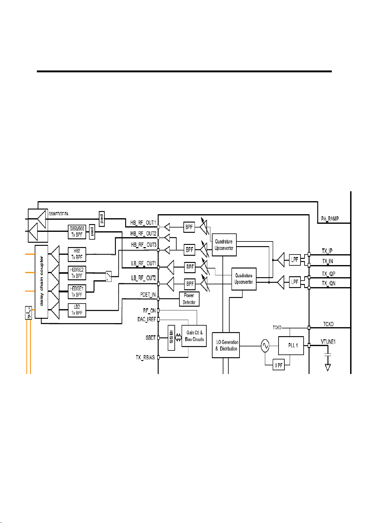
(2) Transmitter Part
The transmit path begins with differential baseband signals (I and Q) from the MSM device.
These analog input signals are buffered, filtered by low-path filter, corrected for DC offsets,
amplified, and then applied to the quadrature upconverter mixers.
The upconverter outputs are amplified by multiple variable gain stages that provide transmit
AGC control. SSBI is used to do the gain control. The specified driver amplifier output level is
achieved while supporting the GSM/EDGE and UMTS transmit standard’s requirements for GSM
ORFS, carrier and image suppression, WCDMA ACLR, spurious emissions, Rx-band noise, etc.
These upconverters translate the polar GMSK-modulated or 8-PSK modulated baseband PM
signals and/or WCDMA baseband signals directly to the RF signals, which are filtered and feed
into the GSM/EDGE polar PA and/or WCDMA PA.
The WCDMA Tx power is coupled back to the RTR6285/RTR6280 internal power detector input
pin, PWD_DET_IN, using a coupler for power measurement.
Figure. 3-5 RTR6285 TRANSMITTER PART
(3) PLLs
Three fully functional fractional-N synthesizers, including VCOs and loop filters, are integrated
within the RTR6285 IC, while the RTR6280 IC has two fractional-N synthesizers. The first
synthesizer (PLL1) creates the transceiver LOs that support the UMTS transmitter, and all four
GSM band receivers and transmitters including: GSM 850, GSM 900, GSM 1800, and GSM
1900.
The second synthesizer (PLL2) provides the LO for the UMTS primary and secondary receivers
(RTR6285 only). The third synthesizer (PLL3) provides the LO for the GPS receiver
Page 19

3. TECHNICAL BRIEF
N
N
Counter
Counter
VCO
VCO
Digital
Logic
Control signal
R
Loop filter
Loop filter
Figure. 3-6 RTR6285 PLLs Block Diagram
(4) Baseband interface
The RTR6285 IC provides the I/Q path to connect MSM system chip for UMTS/GSM TX and RX sig
nals.
The RF IQ signals are demodulated in MSM system chip to data stream then processed by baseba
nd system.
Most control and status commands are communicated through the RTR6285 MSM device-compati
ble SSBI, enabling efficient initialization, WCDMA transmit gain control, control of device operating
modes and parameters, verification of programmed parameters, and frequency lock status reports.
The MSM device SSBI controller is the master while the RTR6285 IC is a slave.
The RTR6285 IC also provides a digital I/O pin for time-critical control signal.
Phase detection
& charge pump
Counter
TCXO
Figure. 3-7 RTR6285 Baseband Interface
Page 20
3. TECHNICAL BRIEF
3.2 Power Amplifier Module
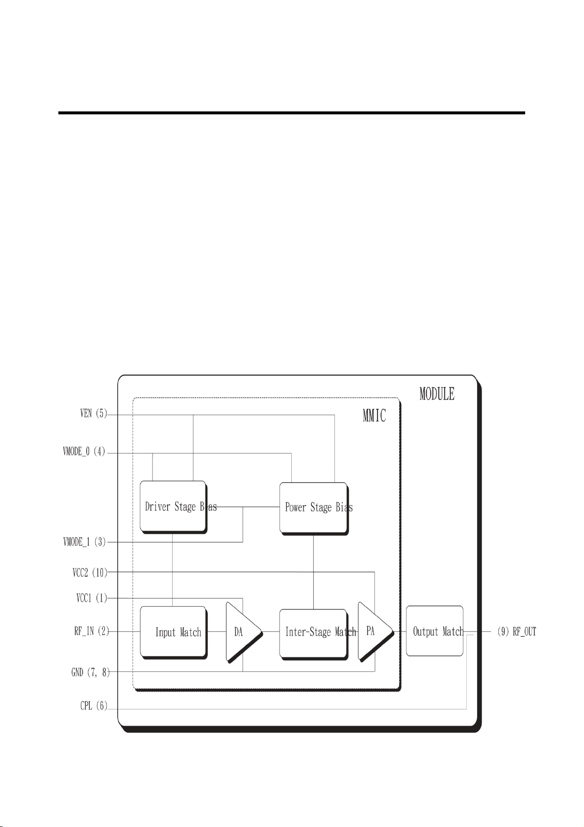
(1) GSM PA (TQM7M5012H, FAR4)
The TQM7M5012H is a ultra-small (5x5mm), GSM/EDGE Polar PAM for handset applications. This
module has been optimized for excellent EDGE efficiency, Rx band noise performance, ACPR and
EVM in an open loop polar modulation environment at EDGE class E2+ operation while maintaining
high GSM/GPRS efficiency.
High reliability is assured by utilizing TriQuint’s 3rd generation InGaP HBT technology and by
TriQuint’s proven module design techniques.
DCS/PCS in
GSM 850/900 in
(2) UMTS PA (FAR3 / SKY17787, FAR2 / SKY77188, FAR1)
A. Band I -- SKY77186, FAR3
The SKY77186 Power Amplifier Module (PAM) is a fully matched 10-pad surface mount module
developed for Wideband Code Division Multiple Access (WCDMA) applications. This small and
efficient module packs full 1920–1980 MHz bandwidth coverage into a single compact package.
Because of high efficiencies attained throughout the entire power range, the SKY77186 delivers
unsurpassed talk-time advantages. The SKY77186 meets the stringent spectral linearity
requirements of High Speed Downlink Packet Access (HSDPA) data transmission with high power
added efficiency. A directional coupler is integrated into the module thus eliminating the need for
any external coupler.
DCS/PCS out
Logic
Power control
GSM 850/900
out
Figure 3-8 GSM PA Functional Block Diagram
Page 21
3. TECHNICAL BRIEF
B. Band II -- SKY77187, FAR2
The SKY77187 Power Amplifier Module (PAM) is a fully matched 10-pad surface mount module
developed for Wideband Code Division Multiple Access (WCDMA) applications. This small and
efficient module packs full 1850–1910 MHz bandwidth coverage into a single compact package.
Because of high efficiencies attained throughout the entire power range, the SKY77187 delivers
unsurpassed talk-time advantages. The SKY77187 meets the stringent spectral linearity
requirements of High Speed Downlink Packet Access (HSDPA) data transmission with high power
added efficiency. A directional coupler is integrated into the module thus eliminating the need for
any external coupler.
C. Band V -- SKY77188, FAR1
The SKY77188 Power Amplifier Module (PAM) is a fully matched 10-pad surface mount module
developed for Wideband Code Division Multiple Access (WCDMA) applications. This small and effic
ient module packs full 824–849 MHz bandwidth coverage into a single compact package. Because
of high efficiencies attained throughout the entire power range, the SKY77188 delivers unsurpasse
d talk-time advantages. The SKY77188 meets the stringent spectral linearity requirements of High
Speed Downlink Packet Access (HSDPA) data transmission with high power added efficiency. A dir
ectional coupler is integrated into the module thus eliminating the need for any external coupler.
Figure 3-9 UMTS PA Block Diagram
Page 22
3. TECHNICAL BRIEF
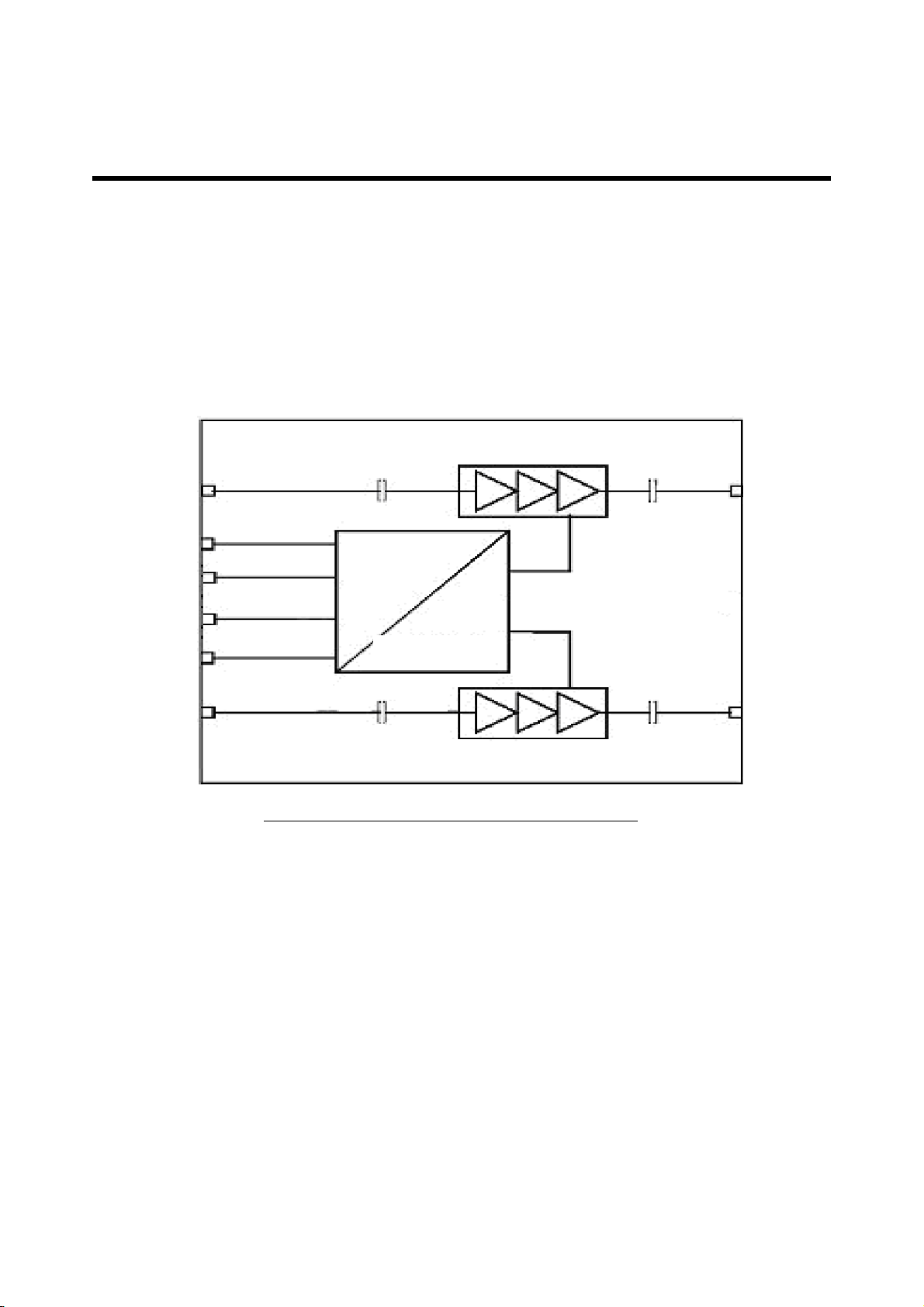
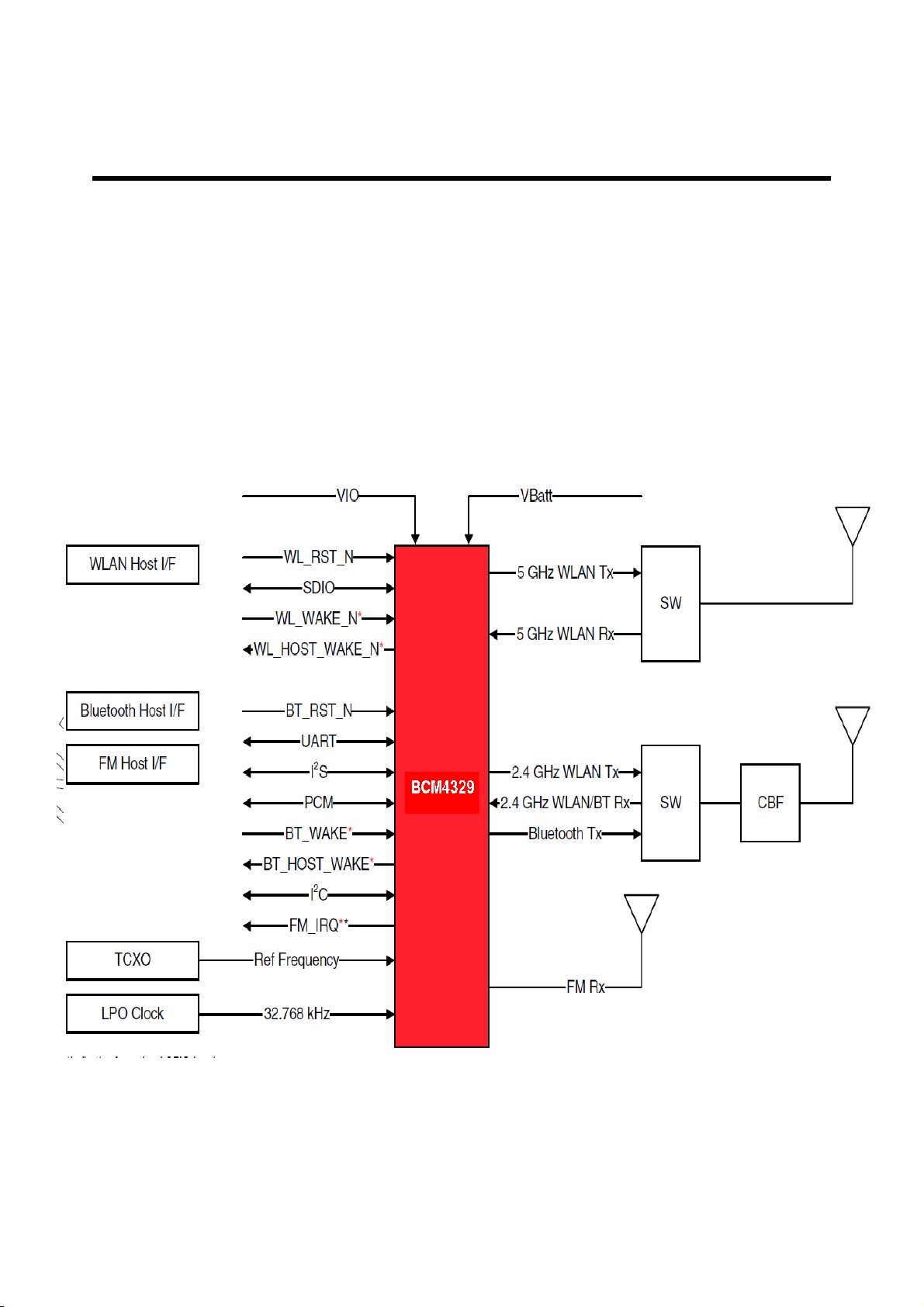
3.3 BT/WiFi/FM (BCM4329, FU1 on Sub board)
The BCM4329 family of single chip devices provides for the highest level of integration for a
mobile or handheld wireless system, with integrated IEEE 802.11 a/b/g, Bluetooth 2.1 + Enhanced
Data Rate (EDR), and FM radio receiver. It provides a compact ultra-small form-factor solution
with minimal external components to drive the costs for mass volumes and allows for flexibility in
size, form, and function of handheld devices. BCM4329 is designed to address the needs of
highly mobile devices that require minimal power consumption and reliable operation.
The BCM4329’s integrated CMOS WLAN 2.4 GHz and 5 GHz power amplifier provide sufficient out
put power to meet the needs of most WLAN devices. Furthermore, the BCM4329’s integrated
buck-boost regulator allows its internal power amplifiers to operate at optimal performance, even
at low Vbat supply voltages.
Figure 3-10 BCM4329 System Diagram
Page 23

3. TECHNICAL BRIEF
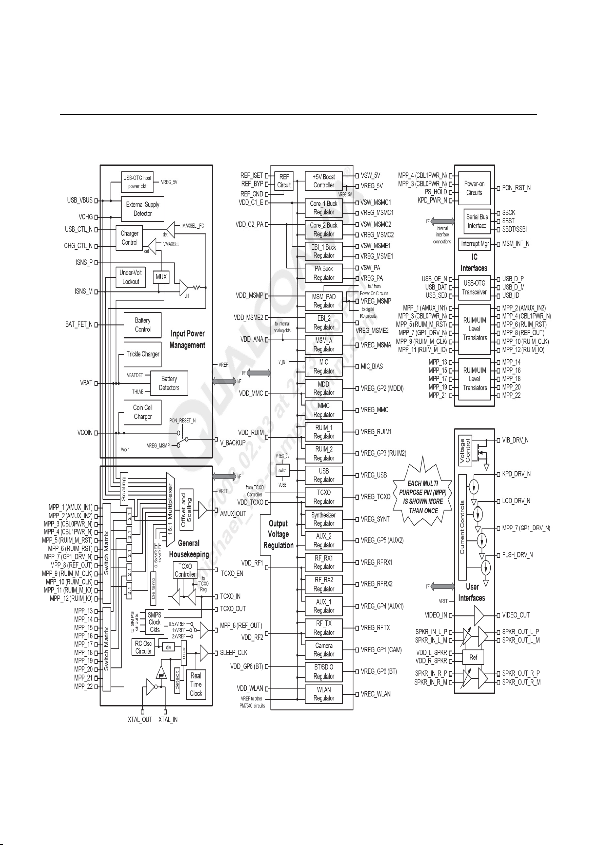
3.4 PMIC (PM7540, U7)
Complete power management, housekeeping, and user interface functions for wireless
devices.
1. Input power management.
z Valid external supply attachment and removal detection
z Supports unregulated external charger supplies and USB supplies as input power
source.
z Supports Lithium-ion main batteries.
z Trickle, constant current, constant voltage, and pulsed charging of the main battery.
z Support coin cell backup battery (including charging)
z Battery voltage detectors with programmable thresholds.
z VDD collapse protection.
z Charger current regulation and real-time monitoring for over current protection.
z Charger transistor protection by power limit control.
z Control drivers for two external pass transistors and one external battery MOSFET.
z Voltages, current and power control loop.
z Automated recovery for sudden momentary power loss.
2. Output voltage regulation
z One boost switch-mode power supply for driving white LED and hosting USB-OTG.
z Four buck, switch-mode power supplies for efficiently generating MSMC1, MSMC2,
MSME and PA supply voltages.
z Supports dynamic voltage scaling (DVS) for MSMC1, MSMC2 and PA outputs.
z 18 low dropout regulator circuits with programmable output voltages, implemented
using three different current ratings: 300mA(four), 150mA(ten) and 50mA(four).
z One MIC bias regulator circuit.
z All regulators can be individually enable /disable for power savings.
z Low-power mode available on most regulators.
z All regulated outputs are derived from a common bandgap reference.
3. Integrated handset-level housekeeping functions reduces external parts count, size and
cost.
z Analog multiplexer selects form five internal and up to 28 external inputs.
z Multiplexer output’s offset and gain are adjusted, increasing the effective ADC
resolution.
z Adjusted multiplexer output is buffered and routed to an MSM device ADC.
z Dual oscillators: a 32.768 kHz off-chip crystal and on-chip RC assure MSM device
sleep clock.
z Crystal oscillator detector and automated switch-over upon lost oscillation.
z Real-time clock tracking time and generating associated alarms.
z ON-chip adjustments minimize crystal oscillator frequency errors.
z Control TCXO warm-up and synchronize, deglitch and buffer the TCXO signal.
z TCXO buffer control for optimal QPH/catnap timing.
z
Multistage over temperature protection.
Page 24

3. TECHNICAL BRIEF
4. Integrated handset-level user interfaces
z Four programmable current sinks recommended as keypad backlight,LCD backlight,
camera flash, and general-purpose drivers.
z Vibration motor driver programmable from 1.2 to 3.1 in 100mV increments.
z Two-channel speaker driver with programmable gain, turn-on time, and muting;
configurable inputs and outputs capable of stereo or mono operation.
z Video (TV) amplifier allows use as a camcorder or for slide presentations.
5. IC-level interfaces
z Configurable SBI for efficient initialization, status, and control
z Supports MSM interrupt processing with an internal manager.
z Many functions monitored and reported through real-time and interrupt status signals.
z Dedicated circuits for controlled power-on sequencing, including the MSM device’s
reset signal.
z Several events continuously monitored for triggering power-on/power-off sequences.
z Supports and orchestrates soft resets.
z USB-OTG transceiver for full-speed and low-speed interfacing of the MSM device to
computers as a USB peripheral, or connecting the MSM device to other peripherals.
z Two sets of RUIM level translators enable MSM device interfacingwith external
modules.
6. 22 multipurpose pins that can be configured as digital or analog I/Os, bidirectional I/Os,
or current sinks; default functions support the two sets of RUIM level translators, poweron circuit, analog multiplexer inputs, an LED driver, and a selectable reference voltage
output.
7. Highly integrated functionality in a small package- 137pin CSP with a several center
ground pins for electrical ground, mechanical stability, and thermal relief.
Page 25
3. TECHNICAL BRIEF
Figure 3-12 PM7540 function block Diagram
Page 26

3. TECHNICAL BRIEF
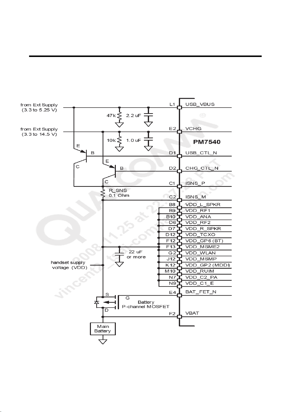
3.5.1 Input power management.
A valid analog voltage at this pin is recognized by the PM7540 IC
VCHG
to be an external supply, and factors into the IC's power
management operating mode.
CHG_CTL_N
USB_VBUS
USB_CTL_N
ISNS_P
ISNS_M
BAT_FET_N
VBAT
VCOIN
V_BACKUP
Control signal for the external pass transistor - a low voltage turns
on the pass transistor.
This pin is configured as an analog input or an analog out
depending upon the type of peripheral device connected. (Don’t use
in the C570)
Control signal for the external USB pass transistor - a low voltage
turns on the pass transistor. (Don’t use in the C570)
The positive current sensor input - connect to the pass transistor
side of the sensor resistor.
The negative current sensor input - connect to the VDD side of the
sensor resistor.
Control signal to the external battery MOSFET; connect directly to
its gate.
Monitors the battery voltage; connect directly to the battery plus
terminal
Connection to the optional coin cell. Provides backup power to the
crystal oscillator and real time clock circuits to maintain time and
alarm functions if a valid external supply or main battery is not
connected.
Connect this pin to the SRAM supply pin. (Don’t use in the C570)
Table 3-1 Input Power Management Pin Description
Page 27
3. TECHNICAL BRIEF
A. Input circuit schematic diagram
Figure 3-13 Input circuit schematic diagram
Page 28

3. TECHNICAL BRIEF
B. External supply detection.
The PM7540 continually monitors external supply voltages (VCHG and VUSB) and the
handset supply voltage (VDD). Internal detector circuit measure these voltages to
recognize when supplies are connected or removed, and verify they are within their valid
ranges when connected.
The PMIC detects when the external supply is removed by monitoring the voltage across
the external PNP pass transistor. The detection circuit begins to close the pass transistor
when the VCHG voltage drops to about 30mV, the detection circuitry cuts the bias to the
pass transistor sp that the removal can be detected.
C. Transistor drivers
Control drivers for the charger pass transistor and the battery MOSFET are included
within the PM7540 device. The driver outputs are applied to the external devices via the
PMIC’s CHG_CTL_N, USB_CTL_N, and BAT_FET_N pins.
D. Voltage regulator
The PM7540 device provides closed-loop control of the pass transistor (via CHG_CTL_N)
to regulate either the handset supply voltage (VDD) when not charging, or the main
battery final voltage (VBAT) when charging. When fast charging is disable, the battery
MOSFET is opened and the voltage regulation point is the ISNS_M pin (VDD). When fast
charging is enable, the VBAT pin is the voltage regulation point.
E. Current regulator
An external sensor resistor is required and must be connected across the ISNS_P and
ISNS_M pins to allow the PM7540 IC to continuously monitor the total handset
electronics plus charger current. If the programmed current threshold is exceeded, the
active pass transistor is forced to a high resistor, disrupting VDD or VBAT regulation but
protecting against excess current.
The same circuits are used to regulate the total handset electronics plus charging
current during the main battery’s constant current charging mode. Either pass transistor
(charger) can be active while the current is regulated----only the appropriate control
pin (CHG_CTL_N) is active.
Page 29

3. TECHNICAL BRIEF
F. Main battery charging
The PM7540 device provides support circuitry for charging a lithium-ion battery, cycling
through as many as four charging techniques: Trickle, constant current, constant voltage
and pulsed.
Charging of a severely depleted battery begins with trickle charging, a mode that limits th
e current and avoids pulling VDD down. Once a minimum battery voltage is established u
sing trickle charging, contact current charging is enable via software to charge the batter
y quickly—this mode is sometimes called fast charging. Once the lithium-ion battery app
roaches its target voltage, the charge is completed using constant voltage.
G. Backup battery charging
Backup battery charging is enable through software control and powered from VBAT. The
on-chip charger is implemented using a programmable voltage regulator and a program
mable series resistor. The MSM device reads the backup battery voltage through the PMI
C’ s analog multiplexer to monitor charging.
Page 30
3. TECHNICAL BRIEF
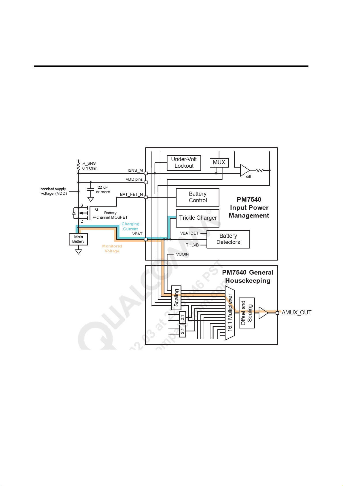
H. Trickle charging
Trickle charging of main battery, enable through MSM control and powered from VDD, is
provide by PM7540 IC. This mode is used to raise a severely depleted battery’s voltage t
o a level sufficient to begin fast charging.
Figure 3-14 Trickle charging
Page 31

3. TECHNICAL BRIEF
I. Constant current charging
The PM7540 IC supports constant current charging of the main battery by closing the bat
tery MOSFET, and closed-loop controlling the active pass transistor (charger or USB). T
he closed-loop control regulates the total current to match the programmed value (IMAX
SEL)
Figure 3-15 Constant current charging
Page 32

3. TECHNICAL BRIEF
J. Constant voltage charging
Once constant current charging of a lithium-ion battery is finished, the charging continu
es using either constant voltage or pulse techniques.
The MSM device and its software determines if and when it is appropriate to begin the co
nstant voltage mode with the charging process. Usually the decision to stop the constant
current mode is based upon the battery voltage reaching a programmed threshold slightl
y above the intended final voltage.
Figure 3-16 Constant voltage charging
Page 33

3. TECHNICAL BRIEF
K. Coin cell charging
Coin cell charging is enable through MSM control; its supply current is sourced from the
main battery through the VBAT pin.
All coin cell charging activity is controlled through software, allowing continuous or perio
dic charging of the coin cell and management of the main battery current.
Figure 3-17 Coin cell charging
Page 34

3. TECHNICAL BRIEF
3.5.2 Output voltage regulation
Twenty-four voltage regulators are provided– all programmable, all derived from a
common bandgap reference circuit.
Two major types of voltage regulator circuits are on-chip: switched-mode power
supplies (SMPS) and linear regulators. There are three types of SMPS supplies: the boost
circuit step up its output voltage relative to the input voltage and is rated for 500mA; the
buck circuits step down their output voltages and are rated for either 300 or 500mA each.
There are four different linear regulator circuit, three categorized by their output current
ratings (300, 150, and 50mA) and the fourth intended for biasingmicrophone.
VSW_5V switching output of the +5V boost SMPS circuit.
VREG_5V Senses the regulated output of the +5V boost SMPS
VSW_MSMC1 Switching output of the MSM core_1 buck SMPS circuit.
VREG_MSMC1 Senses the regulated output of the core_1 buck SMPS
VSW_MSMC2 Switching output of the MSM core_2 buck SMPS circuit.
VREG_MSMC2 Senses the regulated output of the core_2 buck SMPS
VSW_MSME Switching output of the EBI_1 buck SMPS circuit.
VREG_MSME Senses the regulated output of EBI_1 buck SMPS circuit.
VSW_PA Switching output of the PA buck SMPS circuit.
VREG_PA Senses the regulated output of the PA buck SMPS circuit.
Table 3-2 PM7540 Output Voltage Regulation Pin Description
Page 35

3. TECHNICAL BRIEF
VREG_GP1 General-purpose linear regulator output #1
VREG_GP2 General-purpose linear regulator output #2
VREG_GP3 General-purpose linear regulator output #3
VREG_GP4 General-purpose linear regulator output #4
VREG_GP5 General-purpose linear regulator output #5
VREG_GP6 General-purpose linear regulator output #6
VREG_MMC Linear regulator output intended to power MMC circuit.
VREG_MSMA Linear regulator output intended to power MSM device analog function.
VREG_MSME2 Linear regulator output intended to power EBI_2 circuit.
VREG_MSMP Linear regulator output intended to power MSM peripheral functions.
VREG_RFRX1 Linear regulator output intended to power primary receiver circuits.
VREG_RFRX2 Linear regulator output intended to power diversity receiver circuits.
VREG_RFTX Linear regulator output intended to power transmitter circuits.
VREG_RUIM1 Linear regulator output intended to powerRUIM_1 circuits.
VREG_SYNT Linear regulator output intended to power frequency synthesizer circuits.
VREG_TCXO Linear regulator output intended to power VCTCXO circuits.
VREG_USB Linear regulator output intended to power the internal USB transceiver.
VREG_WLAN Linear regulator output intended to power WLAN circuits.
VREG_BIAS Linear regulator output intended to bias MIC circuits.
Table 3-2 PM7540 Output Voltage Regulation Pin Description
Page 36

3. TECHNICAL BRIEF
B. PM7540 voltage regulator circuits
Figure 3-18 Voltage regulator circuit
Page 37

3. TECHNICAL BRIEF
B. PM7540 voltage regulator circuits
Figure 3-19 Voltage regulator circuit
Page 38

3. TECHNICAL BRIEF
C. Voltage regulator summary
Table 3-3 Voltage regulator summary
Page 39

3. TECHNICAL BRIEF
3.5.3 General Housekeeping
Housekeeping functions include an analog multiplexer with gain and offset adjustments;
system clock circuits; real time clock for time and alarm functions; buffered reference
voltage outputs; and over-temperature protection.
TCXO_IN Input from the handset VCTCXO
TCXO_EN
TCXO_OUT Buffered and validated VCTCXO output clock signal
XTAL_IN
SLEEP_CLK Buffered 32.768kHz sleep clock signal;
AMUX_OUT Output of the analog multiplexer.
MPP_1
MPP_2
MPP_8
Control signal from MSM device that enables TCXO
controller tasks.
Connect the 32.768kHz crystal across these pins with
capacitor from each pin to ground.
These are multipurpose pins whose intended functions are the
first and second external inputs to the analog multiplexer.
This is a multipurpose pin whose intended function is a
selectable, buffered version of the internal reference voltages.
Table 3-4 PM7540 general housekeeping pin description
Page 40

3. TECHNICAL BRIEF
A. Analog multiplexer
The PM functions include a 16 to 1 analog multiplexer to select a single analog signal for
routing to the MSM device’s housekeeping analog to digital converter.
The sixteen multiplexer inputs are derived from five internal connections, six hardwired ex
ternal connections, and 22 MPPs that can be configured as multiplexer inputs.
Figure 3-20 Analog multiplexer and associated circuits
Page 41

3. TECHNICAL BRIEF
B. System clocks
The PMIC includes several clock circuits whose outputs are used for general housekeepi
ng functions and elsewhere within the handset system. These circuits include the TCXO
controller and buffers, RC oscillator, 32.768kHz crystal oscillator, SLEEP clock, and SMP
S clocks.
Figure 3-21 System clocks – functional block diagram
Page 42

3. TECHNICAL BRIEF
3.5.4 User interface
The PM7540 IC supports common handset-level user interfaces. Three dedicated current
sinks are intended for driving the keypad backlight, the LCD backlight, and a camera
flash.
Alerting the handset user of incoming calls is supported with vibration and audio driver
circuits. A vibration motor driver, supports silent alarm. A two-channel speaker driver is a
vailable for audible alarms.
KPD_DRV_N is intended to drive the keypad backlight
LCD_DRV_N is intended to drive the LCD backlight
FLSH_DRV_N is intended to drive high-voltage, high-current white or blue LEDs often
used as a camera flash.
SPKR_IN_L_M
Minus and plus inputs to the left speaker driver circuit.
SPKR_IN_L_P
SPKR_OUT_L_M
Minus and plus outputs from the left speaker driver circuit.
SPKR_OUT_L_P
SPKR_IN_R_P
Minus and plus inputs to the right speaker driver circuit.
SPKR_IN_R_M
SPKR_OUT_R_M
Minus and plus outputs from the right speaker driver circuit.
SPKR_OUT_R_P
VIDEO_IN Video amplifier output
VIDEO_OUT Video amplifier output.
VIB_DRV_N Vibration motor driver output
KPD_DRV_N Programmable current sink intended to support keypad backlights.
LCD_DRV_N Programmable current sink intended to support keypad backlights.
FLSH_DRV_N Programmable current sink intended to support a camera flash strobe.
MPP_7
This is a multipurpose pin whose intended function is the programmable
current sink intended to support general-purpose LED or backlight devices.
Table 3-5 PM7540 user interface pin description
Page 43

3. TECHNICAL BRIEF
A. Current driver
The four backlight or LED driver are independently programmable. Three drivers are inten
ded for specific applications and are named accordingly:
KPD_DRV_N is intended to drive the keypad backlight
LCD_DRV_N is intended to drive the LCD backlight
FLSH_DRV_N is intended to drive high-voltage, high-current white or blue LEDs often
used as a camera flash.
Figure 3-22 Current driver
B. Vibration motor driver
The PM7540 IC supports silent incoming call with its vibrator motor driver. The vibrator dr
iver is a programmable voltage output that is referenced to VDD; when off, its output volt
age is VDD. The motor is connected between VDD and pin N2; the voltage across the m
otor is Vm=VDD- Vout where Vout is the PM7540 IC voltage at pin N2.
Figure 3-23 Vibrator motor driver
Page 44

3. TECHNICAL BRIEF
C. Speaker driver
The PM7540 IC includes a stereo speaker driver with variable gain. The input can be conf
igured for mono differential or stereo single-ended operation. Each channel’s output is c
onfigured differentially, delivering 500mW to each 8-ohm speaker.
Figure 3-24 Speaker driver
Page 45

3. TECHNICAL BRIEF
3.5.5 IC-level interface
The PM7540 IC-level interface circuits include power-on circuits, the SBI, the interrupt
manager, a USB-OTG transceiver, and RUIM level translators.
KPD_PWR_N Connect to the keypad power button.
PON_RESET_N
Connect this pin to MSM device's RESIN_N pin. During a
PMIC power-on sequence, this signal is driven low to
initial as MSM power-on reset.
PS_HOLD
MPP_3
MPP_4
SBST
SBCK
SBDT/SSBI
MSM_INT_N
USB_ID
USB_D_P
USB_D_M
USB_OE_N
Connect this pin to the MSM device's PS_HOLD output
pin.
These two pins are multipurpose pins with the intended
function of recognizing a serial cable insertion and
initialing the power-on sequence.
3-line SBI-- data , clock and strobe signals.
For later MSM device: Single-wire SBI.
PMIC interrupt status is reported to MSM device using this
signal. Logic low signals that an interrupt event has
occurred.
Analog input used to sense whether a peripheral device is
connected and if connected, to determine the peripheral
type. (Don’t use in the
Plus line of the differential, bidirectional USB signal
to/from the peripheral device. (Don’t use in the
Minus line of the differential, bidirectional USB signal
to/from the peripheral device. (Don’t use in the
USB output enable signal .(Don’t use in the
C570
)
C570
)
C570
)
C570
)
USB_DAT
USB_SE0
Plus line of the digital differential, bidirectional USB signal
to/from the MSM device. (Don’t use in the
Minus line of the digital differential, bidirectional USB
signal to/from the MSM device. (Don’t use in the
C570
)
C570
Table 3-4 PM7540 IC-level pin description
)
Page 46

3. TECHNICAL BRIEF
MPP_11
(RUIM_M_IO)
MPP_12
(RUIM_IO)
MPP_9
(RUIM_M_CLK)
MPP_10
(RUIM_CLK)
MPP_5
(RUIM_M_RST)
MPP_6
(RUIM_RST)
MPP_1 to
MPP_22
This pair's intended configuration is the bidirectional RUIM I/O
level translator.
This pair's intended configuration is the RUIM clock level
translator.
This pair's intended configuration is the RUIM reset level
translator.
These multipurpose pins are software configurable with the
following options:
● Digital input
● Digital output.
● Digital level translator
● Analog input
● Analog output
● Current sink
VDD_ANA Input supply voltage for the MSMA linear regulator circuits.
VDD_C1_E Input supply voltage for core_1 and EBI_1 buck converter circuits.
VDD_C2_PA Input supply voltage for core_2 and PA buck converter circuits.
VDD_GP2
VDD_GP6 Input supply voltage for the BT linear regulator circuit.
VDD_MSME2 Input supply voltage for the EBI_2 linear regulator circuit.
VDD_MSMP Input supply voltage for the MSMP linear regulator circuit.
VDD_RF1
VDD_RF2
VDD_RUIM
VDD_L_SPKR Power supply for left speaker driver circuit.
VDD_R_SPKR Power supply for right speaker driver circuit.
VDD_TCXO
VDD_WLAN Input supply voltage for the WLAN linear regulator circuit.
Input supply voltage for the MMC and GP2 linear regulator
circuits.
Input supply voltage for the RF_RX1, RF_RX2, and AUX_1 linear
regulator circuit.
Input supply voltage for the RF_TX and GP1 linear regulator
circuit.
Input supply voltage for the RUIM_1 and RUIM_2 linear regulator
circuit.
Input supply voltage for the TCXO, SYNT, and AUX_2 linear
regulator circuit.
Table 3-4 PM7540 IC-level pin description
Page 47

3. TECHNICAL BRIEF
A. Power-on circuits and the power sequences
Dedicated circuits continuously monitor five events that might trigger a power-on
sequence. If any of the five events occur these circuits power on the PMIC, determine
the handset’s available power sources, enable the correct source, and take the MSM
device out of reset.
The inputs to the power-on circuit (MPP3, MPP4, PS_HOLD, and KPDPWR_N) are basic
digital control signals and the only external output is PON_RESET_N.
Figure 3-25 High-level power sequences timing diagram
Page 48

3. TECHNICAL BRIEF
B. Serial bus interface (SBI)
The PM7540 IC allow two serial bus interface (SBI) implementations:
z A 3-wire SBI that support earlier MSM devices
z An SSBI that supports later MSM devices.
In both case, the SBI provides efficient initialization, status, and control communications.
Configurable device parameters are set through SBI control registers, while many other
registers are available to report parameter settings, device status, and interrupt events.
C. Interrupt manager
The PM7540 interrupt manager receivers internal report on numerous functions and
conveys real-time and latched status signals to the MSM device, thereby supporting the
MSM device’s interrupt processing.
The interrupt manager is an embedded function that does not require I/O specifications.
All of its controls and output data accessed via the SBI.
D. Universal serial bus/on-the-go
The PM7540 includes an integrated universal serial bus/on-the-go (USB-OTG)
transceiver on-chip. This transceiver operates at USB low speed (1.5Mbit/sec) and USB
full-speed (12Mbit/sec). It is complaint with USB 2.0 specification, and the OTG
Supplement.
E. RUIM level translators
All MPP pairs can be configured as RUIM level translators; three pairs are intended to be
used as level translators that interface the handset’s MSM device to an external RUIM
module: MPP5/6, MPP9/10 and MPP11/12.
Page 49

3. TECHNICAL BRIEF
Figure 3-26 RUIM level translators
Page 50

3. TECHNICAL BRIEF
3.6 MSM7227 (U1)
1. Four integrated processors
z ARM1136JF-S for application functions.
z ARM926EJ-S for modem functions.
z The low-power, high-performance QDSP5000 application digital signal processor.
z The QDSP4000 modem digital signal processor.
2. Memory support
z 200MHz bus clock for DDR SDRAM.
z Dual-memory buses separating the high-speed memory subsystem (EBI1) from low-
speed peripherals (EBI2) such as LCD panels.
z 1.8V or 2.6V memory interface support
z NAND flash memory interface
z Boot from NAND/OneNAND
3. Air interface
z WCDMA: HSDPA, HSUPA, R99.
z GSM/GPRS/EDGE
z GPS position location: simultaneous-GPS and time-multiplexed GPS architectures.
z Bluetooth 2.1 EDR device.
4. RF and PM interfaces
5. MDDI
6. Image processing
7. Video
8. Graphics
z 2D and 3D rendering
z 3.5M 3D-lighted triangles/sec
z Resolution support: up to WVGA
z Frame rate: (MPEG4/H.263 30fps@WVGA and H.264@15fps)
z 3D pixel fill rate: 133MP/sec.
9. Audio
z Vocoder support
z Voice recognition, including speaker-independent digit dialing
z Acoustic echo cancellation.
z PureVoice Audio AGC.
z Internal vocoder supporting 13Kbps Pure Voice.
z Standard MIDI with 16 voices.
z 72-tone CMX
10. Connectivity
z High-speed on the go universal serial bus. (HS USB OTG)
z Three universal asynchronous receiver transmitter (UART) serial ports.
z Two data mover (DM) high speed UARTs (4Mbps)
z USIM controller (via second or third UART)
z USB-UICC
z Four integrated 4-bit secure digital (SD) controller for SD/mini SD cards and SDIO
z Transport stream interface (TSIF) for reception of digital mobile broadcast signals
Page 51

3. TECHNICAL BRIEF
11. Internal functions
z Secure boot: protects against re-flashing attacks.
z Secure component framework
z Secure storage
z Unchangeable hardware ID unique to each MSM device.
12. GPIOs
z The MSM7227 IC includes 133 general-purpose I/O pins.
Page 52

3. TECHNICAL BRIEF
Figure 3-24 MSM7227 functional block diagram
Page 53

3. TECHNICAL BRIEF
3.6.1 MSM7227 architecture
The MSM7227 integrates multiple microprocessors on chip: two ARM processors and two D
SP processors.
Modem subsystem
z ARM926EJ-S microprocessor
z QDSP4 (mDSP) processor
Modem subsystem
z ARM1136JF-S microprocessor
z QDSP5 (aDSP) processor
Figure 3-27 MSM7227 high-level architecture
Page 54

3. TECHNICAL BRIEF
A. Modem subsystem
The modem subsystem is defined as everything under direct or indirect control of the mode
m processor. It includes all blocks that provide modem functionality directly (such as WCD
MA modulation and demodulation, searching, GPS, GSM modulation and demodulation, etc.)
and all blocks that support primary modem functionality, such as that modem DSP, modem
AHB bus, sleep controller, interrupt controller, etc.
The MSM7227 modem subsystem consists of the following components:
An ARM926EJ-S as the main modem processor.
A modem-to-applications bridge that connects the modem subsystem to the application
subsystem
A modem-to-peripheral bridge that connects the modem subsystem to the peripheral
subsystem.
A modem DSP that controls the operation of the concurrent modem hardware blocks and
assists with symbol level processing of the physical layer traffic.
A 64KB secure BOOT ROM containing the primary boot loader for the ARM926EJ-S
processor.
An internal RAM used by the modem processor for interprocessor communication with the
applications.
A security mode control (SMC) block containing, among other things, electrical fuses
(Q fuses) that are used to disable specific functionality.
An always-on modem power manager block in the always-on power domain to control p
ower collapsing of the MSM7227 modem subsystem.
Figure 3-28 MSM7227 Modem subsystem function block diagram
Page 55

3. TECHNICAL BRIEF
B. Peripheral Bus
The peripheral bus enables bus masters to connect with numerous peripheral device and
lower bandwidth memories both within and external to the MSM7227 IC, thereby offloading t
he buses to the stacked memory interface (SMI) and external bus interface a (EBI1).
Five bus masters are supported: the modem processor, applications processor, application
s data mover, applications DSP, and the mobile display processor (MDP). The peripheral
bus slave devices exist within the bus subsystem, applications subsystem, and graphics
subsystem.
Figure 3-29 Peripheral bus connection diagram
Page 56

3. TECHNICAL BRIEF
C. Application Subsystem
The MSM7227 application subsystem consists of the following components.
An ARM1136 as the main application processor, with its supporting watchdog, clock and
timers.
An applications-to-modem bridge that connects the application subsystem to the modem
subsystem.
An application-to-peripheral bridge that connects the application subsystem to the periph
eral subsystem.
An application DSP, the QDSP5 with 128KB of memory that handles applications such as
vocoder, video and graphics.
A dedicated application data mover.
Connectivity blocks that support various applications such as USB.
Two MDDI host blocks and the MDP block that support various LCD display.
Video blocks such as an MDDI client, video front-end and TV out to support camera and
other video functions.
Figure 3-30 Application subsystem block diagram
Page 57

3. TECHNICAL BRIEF
D. AXI buses: EBI1
To satisfy the requirement of high performance data transfer, a 64-bit advanced extensible
interface (AXI) bus is used as a standard bus interface between the bus masters and slaves.
The bus masters are connected to the external high-speed memory interfaces, EBI1.
The various MSM7227 bus masters that can access the high speed memory interfaces
via the AXI buses.
Figure 3-31 AXI bus connection diagram
Page 58

3. TECHNICAL BRIEF
3.6.2 Memory Support
The MSM7227 IC provides two categories of memory interfaces: high-speed and low-speed.
High-speed interfaces are needed for the multiple on-chip ARM processors, high-performa
nce graphics, and video applications. The low-speed interface supports memory devices
such as NAND flash and asynchronous SRAM, peripheral devices such as LCD, and the
FLO receiver for multicast reception.
To support the high bandwidth, high density, and low latency requirements of the advanced
on-chip application, the MSM7227 IC has a 64-bit high-speed, high-performance memory
slave interfaces: the external bus interface 1 (EBI1).
The MSM7227 includes the low-speed EBI2 to support peripheral devices, more memory
devices, and the FLO receiver for multicast reception.
Figure 3-32 MSM7227 memory map
Page 59

3. TECHNICAL BRIEF
A. High-speed memory interface (EBI1)
General EBI1 features include:
z Support for only low-power memories at 1.8V I/O power supply voltage
z AXI bus frequencies up to 200MHz
z DDR SDRAM clock rates from 9.6MHz to 200MHz
z A 16/32 bit static and dynamic memory interface
EBI1 connections include:
z Two-16 bit address bus
z One-32 bit bidirectional data bus
z Other bus signaling
z Data strobes, data masks, clocks, chip selects, enable, etc.
Page 60

3. TECHNICAL BRIEF
B. Pins Description.
PIN Symbol Description
W22 EBI1_ADR_13
AC26 EBI1_ADR_12
V23 EBI1_ADR_11
AB26 EBI1_ADR_10
AB25 EBI1_ADR_9
AA23 EBI1_ADR_8
AA25 EBI1_ADR_7
Y26 EBI1_ADR_6
Y23 EBI1_ADR_5
T17 EBI1_ADR_4
Y22 EBI1_ADR_3
W23 EBI1_ADR_2
AA26 EBI1_ADR_1
V20 EBI1_ADR_0
28bit EBI1 address bus.
Page 61

3. TECHNICAL BRIEF
PIN Symbol Description
J26 EBI1_DQ31
K20 EBI1_DQ30
J20 EBI1_DQ29
J23 EBI1_DQ28
J22 EBI1_DQ27
K19 EBI1_DQ26
K26 EBI1_DQ25
L22 EBI1_DQ24
L19 EBI1_DQ23
L23 EBI1_DQ22
L20 EBI1_DQ21
M19 EBI1_DQ20
L26 EBI1_DQ19
M26 EBI1_DQ18
M22 EBI1_DQ17
M23 EBI1_DQ16
N26 EBI1_DQ15
N19 EBI1_DQ14
N20 EBI1_DQ13
P26 EBI1_DQ12
R26 EBI1_DQ11
P19 EBI1_DQ10
R25 EBI1_DQ9
T26 EBI1_DQ8
R22 EBI1_DQ7
R23 EBI1_DQ6
R20 EBI1_DQ5
T23 EBI1_DQ4
T22 EBI1_DQ3
32bit EBI1 DATA bus.
U25 EBI1_DQ2
U23 EBI1_DQ1
U22 EBI1_DQ0
Page 62

3. TECHNICAL BRIEF
PIN Symbol Description
H26 EBI1_DQS3
L25 EBI1_DQS2
P20 EBI1_DQS1
U26 EBI1_DQS0
J25 EBI1_DM3
M20 EBI1_DM2
N25 EBI1_DM1
V26 EBI1_DM0
W26 EBI1_DCLK
W25 EBI1_DCLKB
V19 EBI1_BA0_N DDR bank address
AC25 EBI1_BA1_N DDR bank address
U19 EBI1_CS1_N
U20 EBI1_CS0_N
R19 EBI1_CKE1
T19 EBI1_CKE0
T20 EBI1_RAS_N DDR Row select
N17 EBI1_CAS_N DDR Column select
EBI1 data strobes
EBI1 data masks
Differential clock for DDR SDRAM
DDR SDRAM chip select
DDR clock enables
AB23 EBI1_WE_N Write enable
AD26 EBI1_OE_N Output enable
Page 63

3. TECHNICAL BRIEF
3.6.3 Low-speed memory interface (EBI2)
The external bus interface 2 (EBI2) is the second of two MSM7227 external memory interfac
e. EBI2 provides the interface for slow peripheral devices such as LCD, NAND flash memory,
and the FLO receiver.
EBI2 feature include:
The MSM7227 EBI2 interface supports asynchronous memory devices such as FLA
SH and SRAM (16bit and 8bit). Page mode is NOT supported.
z Programmable wait states for access, hold, and recovery on all chip selects.
z Bus sizing operations allow WORD, HWORD, and BYTE accesses to 16 and 8 bit me
mory.
z Insertion of recovery/turnover wait states (RECOV_CYCLES) to the beginning of the c
urrent chip select access when the previous access was a read to a different chip sel
ect, or a when the current access is a write and the previous access was a read to th
e same chip select.
z Addressing to chip select assertion setup wait states (ADDR_CS_SETUP) at the begin
ning of the access.
z RD_ACTIVE and WR_ACTIVE define the minimum assertion time for read and write res
pectively.
z Since the RECOV_CYCLES and ADDR_CS_SETUP wait states are applied at the begin
ning of the access, only the field with the greatest number of wait states take effect.
z Hold time between WE_N rising and the address/CS_N/data signals changing (WR_C
S_HOLD wait states), as required by specific type of peripherals. The mini value is RD
_CS_HOLD=0.
z Supports byte-addressable 16 bit device (UB_N and LB_N signals).
The EBI2 interface not only supports memory devices, but can be used for parallel, port
mapped LCD. The related features include:
z Support for both Motorola and Intel timing types (24bit, 18bit and 16bit)
z Bus sizing operations allow 18bit write accesses to an 18 bit LCD interface, WORD a
nd HWORD accesses to parallel 16 bit data parallel interface, and WORD, HWORD, an
d BYTE access to parallel 8 bit data interface.
z System WORD, HWORD, and BYTE accesses to 16 bit and 8 bit wide devices on all
chip selects.
z Support for 18 bit wide device is write mode only.
z Access times of up to 2000ns (at 66MHz AHB bus speed)
z Specific to Intel Interface mode
z EBI2 I/O are compatible with either 1.8V or 2.6V pad power supply voltage.
z The EBI2 supports any generic external peripheral whose interface timing is similar to
asynchronous memories.
EBI2 connections
z 20 bit address bus
z 16 bit bidirectional data bus
z Chip selects, enables, etc.
Page 64

3. TECHNICAL BRIEF
A. Pins Description.
PIN Symbol Description
B18 EBI2_ADR9 Reserved
B25 EBI2_ADR8 Reserved
F21 EBI2_ADR7 Reserved
B20 EBI2_ADR6 Reserved
F20 EBI2_ADR5 Reserved
H17 EBI2_ADR4 Reserved
E20 EBI2_ADR3 Reserved
C20 EBI2_ADR2 Reserved
C18 EBI2_ADR1 Reserved
F18 EBI2_ADR0 Reserved
B21 EBI2_DATA15
B22 EBI2_DATA14
C21 EBI2_DATA13
E21 EBI2_DATA12
C22 EBI2_DATA11
C24 EBI2_DATA10
E26 EBI2_DATA9
B24 EBI2_DATA8
F25 EBI2_DATA7
C26 EBI2_DATA6
D26 EBI2_DATA5
C23 EBI2_DATA4
B23 EBI2_DATA3
C25 EBI2_DATA2
D25 EBI2_DATA1
E23 EBI2_DATA1
16 bit data bus
Page 65

3. TECHNICAL BRIEF
PIN Symbol Description
L16 EBI2_LB_N NAND flash address latch enable
C19 EBI2_UB_N NAND flash Command latch enable
H19 EBI2_WE_N NAND flash Write enable
B19 EBI2_OE_N NAND flash Read enable
H20 EBI2_CS7_N Chip select
J18 EBI2_CS6_N Chip select 1st LCD
J17 EBI2_CS5_N Chip select
H23 EBI2_CS4_N Chip select
F22 EBI2_CS1_N Chip select 2nd NAND
F23 EBI2_CS0_N Chip select 1st NAND
G25 EBI2_BUSY0_N Busy signal 1st NAND
Page 66

3. TECHNICAL BRIEF
3.6.4 Housekeeping ADC
The MSM7227 device has an on-chip 12 bit analog to digital converter (ADC) that is availabl
e for digitizing analog signals representing parameter such as battery voltage, temperature,
and RF power levels. These parameters support handset-level housekeeping functions-vari
ous tasks that must be performed to keep the “house”, or handset, in order. Thus the term h
ousekeeping ADC (HKADC) is used. The ADC is also fro touch screen purpose and hence is
named the TSHKADC.
The MSM7227 TSHKADC is a 12 bit successive approximation circuit. The resolution of ADC
is programmable and can operation in one of the following mode: 12 bit, 10 bit or 8 bit. The
ADC will operate in 8 bit and 10 bit mode during housekeeping applications and will operate
in 12 bit mode only during touch screen application.
Figure 3-33 HKADC function block diagram
Page 67

3. TECHNICAL BRIEF
3.6.5 MDDI and MDP
The mobile display digital interface (MDDI) is used for communications between the
MSM7227 IC and display devices and/or a camera. A mobile display processor (MDP) is
also provide a hardware accelerator that improves processing speeds and expands
compatibility to include the EBI2 parallel interface.
A. MDDI
The MDDI is a cost effective, low power solution that enables high-speed short range com
munication between the MSM and either display devices and/or a camera using digital pack
et data links. MDDI simplifies the interconnection, reduces its cost, and improves reliability.
The devices connected by the MDDI link are called the host and client. Data going from the
host to the client travels in the forward direction, and data from the client to the host travels
in the reserve direction. The host always drives the strobe to the client, even when reserve d
ata packets are sent. Data can flow in both the forward and reverse directions over the data
pairs, although the host is always the master of the data link.
When interfacing to an LCD, the mobile device is the MDDI host and is the master of the co
mmunication link. When interfacing to a camera, the mobile device is the MDDI client and th
e camera is the host (and master of the link).
1. Pins Description.
PIN Symbol Description
AD13 MDDI_P_STB_N
AE13 MDDI_P_STB_N
AD14 MDDI_P_DATA_N
AE14 MDDI_P_DATA_P
AG15 MDDI_C_STB_N
AH15 MDDI_C_STB_P
AG14 MDDI_C_DATA0_N
AH14 MDDI_C_DATA0_P
AG13 MDDI_C_DATA1_N
AH13 MDDI_C_DATA1_P
AB14 MDDI_E_STB_N
AA14 MDDI_E_STB_P
AA15 MDDI_E_DATA_N
AB15 MDDI_E_DATA_P
LCD differential strobe pair
LCD differential data pair
Camera differential strobe pair
Camera differential data pair 0
Camera differential data pair 1
Peripheral differential strobe pair
Peripheral differential data pair
AD15 VDD_MDDI MDDI power supply
AE15 VSS_MDDI MDDI ground
Page 68

3. TECHNICAL BRIEF
3.6.6 Image Processing
There are two major functional blocks with the MSM7227 IC’s image processing feature: the
camera interface and TV out (or video out) interface.
A. Camera interface
The camera interface is intended for direct connection of a camera sensor to the MSM7227
device. It is used primarily in Qcamera, Qcamcorder, Qtv, and Qvideophone application. Th
e MSM device will accept raw Bayer pattern data, execute the required image processing, a
nd prepare the image for capture or transmission. The MSM device is also capable of suppo
rting a YUV 4:2:2 input from the sensor.
A.1 CAMIF connections
Camera interface connections include:
12bit data bus for the pixel data information
Horizontal and veritical synchronization signals
Two-wire I2C bus as a control path between the MSM device and the camera module.
dedicated master and pixel clock signals.
two hardware-controlled synchronous control outputs (fro shutter and flash)
two pairs of hardware-controlled asynchronous control output (for auto-focus motors an
d zoom).
Page 69

3. TECHNICAL BRIEF
Figure 3-34 Parallel camera interface connections
Page 70

3. TECHNICAL BRIEF
A.2 Pin Description
PIN Symbol Description
M8 CAM_DATA[11]
M7 CAM_DATA[10]
L8 CAM_DATA[9]
M1 CAM_DATA[8]
N8 CAM_DATA[7]
L5 CAM_DATA[6]
N7 CAM_DATA[5]
L7 CAM_DATA[4]
M5 CAM_DATA[3]
M4 CAM_DATA[2]
L2 CAM_DATA[1]
M2 CAM_DATA[0]
P5 CAM_PCLK Clock pixel input: data, vsync, and hsync signals
P11 CAM_HSYNC_IN Parallel camera horizontal sync input
M11 CAM_VSYNC_IN Parallel camera vertical sync input
N11 CAM_MCLK Synchronization clock for sensors without their own
T11 AUX_I2C_SCL Auxiliary I2C clock
N5 AUX_I2C_SDA Auxiliary I2C data
l$4 CAM_MRST Software-controlled camera reset control signal
AD1 SYNC_TIMER1 Camera control, synchronous timer output 1
AB20 SYNC_TIMER2 Camera control, synchronous timer output 2
AD17 ASYNE_TIMER1A Camera control, asynchronous timer output 1
Parallel camera interface pixel data input
AB17 ASYNC_TIMER1B Camera control, asynchronous timer output 1
AE19 ASYNC_TIMER2A Camera control, asynchronous timer output 2
AA19 ASYNC_TIMER2B Camera control, asynchronous timer output 2
Page 71

3. TECHNICAL BRIEF
3.6.7 Audio
The MSM7227 audio front comprises the stereo wideband codec, PCMinterface, and
additional DSP audio processing.
Figure 3-35 Codec, audio DSP, and PCM interface
Page 72

3. TECHNICAL BRIEF
A. Audio connections
MSM7227 audio connections fall primarily into seven categories:
Microphone inputs
Auxiliary input
Line inputs
Earphone outputs
Stereo headphone outputs
Auxiliary output
Line outputs
Figure 3-36 Analog codec front end with audio connections
Page 73

3. TECHNICAL BRIEF
3.6.8 Connectivity
The MSM7227 supports many interfaces that provide handset users with connectivity to othe
r people and data systems.
Keypad interface
MMC/SD/SDIO
High-speed USB
UARTs
USIM
USB-UICC
transport stream interface for digital mobile broadcast
Touchscreen
I2C interface
A. Keypad interface
The MSM7227 provides a keypad interface that supports up to 6X6 or 7X5 keypad matrices.
One set of MSM pins is connected to the keypad’s columns and is used for sensing; anothe
r set of pins is connected to the keypad’s row and is used for driving. The sensed columns r
eveal when any keypad button is pressed, and then the rows are driven to determine precise
ly which keypad button was pressed.
Figure 3-37 6 X 6 matrix
Page 74

3. TECHNICAL BRIEF
B. Pin Description
PIN Symbol Description
AH20 Keypad[11] Driven keypad line
AA20 Keypad[10] Driven keypad line
AE20 Keypad[9] Driven keypad line
AD20 Keypad[8] Driven keypad line
AG22 Keypad[7] Driven keypad line
AE26 Keypad[6] Configurable keypad line; driven or sensed
AH22 Keypad[5] Configurable keypad line; driven or sensed
AD21 Keypad[4] Sensed keypad line
AE22 Keypad[3] Sensed keypad line
AB21 Keypad[2] Sensed keypad line
AG23 Keypad[1] Sensed keypad line
AB22 Keypad[0] Sensed keypad line
Page 75

3. TECHNICAL BRIEF
C. MMC/SD/SDIO
A secure digital (SD) memory card is a flash-based memory card specifically designed to m
eet the security, capacity, performance, and environmental requirements inherent to newly e
merging audio and video consumer electronic devices. The physical form factor, pin assign
ments, and data transfer protocol are forward-compatible with the multimedia card (MMC)
while including some enhancements.
D. Pin Description
PIN Symbol Description
AA11 SDC1_DATA[3] SDC1 data bit #3
AH8 SDC1_DATA[2] SDC1 data bit #2
V13 SDC1_DATA[1] SDC1 data bit #1
AD11 SDC1_DATA[0] SDC1 data bit #0
AE10 SDC1_CMD SDC1 command and response bit
AB11 SDC1_CLK SDC1 clock
Figure 3-38 SDCC architecture
SDC1
Page 76

3. TECHNICAL BRIEF
Pin Description
PIN Symbol Description
AA13 SDC2_DATA[3] SDC2 data bit #3
AE12 SDC2_DATA[2] SDC2 data bit #2
V15 SDC2_DATA[1] SDC2 data bit #1
V14 SDC2_DATA[0] SDC2 data bit #0
AA12 SDC2_CMD SDC2 command and response bit
AE11 SDC2_CLK SDC2 clock
AB16 SDC3_DATA[3] SDC3 data bit #3
AE16 SDC3_DATA[2] SDC3 data bit #2
SDC2
SDC3
V16 SDC3_DATA[1] SDC3 data bit #1
AD16 SDC3_DATA[0] SDC3 data bit #0
AG16 SDC3_CMD SDC3 command and response bit
AA16 SDC3_CLK SDC3 clock
SDC4
AE17 SDC4_DATA[3] SDC4 data bit #3
AA18 SDC4_DATA[2] SDC4 data bit #2
AG18 SDC4_DATA[1] SDC4 data bit #1
V17 SDC4_DATA[0] SDC4 data bit #0
AB24 SDC4_CMD SDC4 command and response bit
AB25 SDC4_CLK SDC4 clock
Page 77

3. TECHNICAL BRIEF
E. USB
The universal serial bus (USB) is an interconnection standard widely supported by the electr
onic industry. The USB 2.0 spec defines data rates as low-speed (1.5 Mbps), full-speed (1
2 Mbps) and high-speed (480 Mbps).
The MSM7227 device contains a new USB high-speed function that is based on a embedde
d UTMI+core with a UTMI+ low pin interface (ULPI) compatible port. The MSM device’s ULPI
interface connects to an external ULPI PHY chip to complete the design. The ULPI core em
bedded in the MSM along with the PM7540 and a USB high-speed PHY IC provide support f
or the high-speed interface.
F. Pin Description
PIN Symbol Description
K1 USBH_CLK Input clock from PHY
U7 USBH_DIR
V12 USBH_NEXT Used by the PHY to throttle data.
J8 USBH_STOP
L14 USBH_DATA[7] Bi-directional data pin
L13 USBH_DATA[6] Bi-directional data pin
L12 USBH_DATA[5] Bi-directional data pin
K8 USBH_DATA[4] Bi-directional data pin
K7 USBH_DATA[3] Bi-directional data pin
K5 USBH_DATA[2] Bi-directional data pin
K4 USBH_DATA[1] Bi-directional data pin
M12 USBH_DATA[0] Bi-directional data pin
Controls the direction of USBH_DATA. When high , data is drive
n into the MSM.
Signals the end of a USB transmit packet or a register write oper
ation, and optionally tops any receiver.
Page 78

3. TECHNICAL BRIEF
G. Universal Asynchronous Receiver Transmitters
The MSM7227 is capable of providing up to four Universal Asynchronous Receiver Transmitt
er (UART) ports. Each MSM7227 UART communicates with serial data ports that conform to
the RS-232 interface protocol.
Support for three UART interfaces in parallel with the followingrequirements:
UART1: High speed, maximum of up to 4Mbps using the UART1DM data mover interface
and up to 230 kbps for data services using the UART1 interface
UART2DM: high speed maximum of up to 4Mbps using the data mover interface
UART2: Maximum speed of 115 kbps
UART3: Maximum speed of 115 kbps
Figure 3-39 UART functional block diagram
Page 79

3. TECHNICAL BRIEF
H. Pin Description
PIN Symbol Description
UART1 or UART1DM
AA10 UART1_RFR_N Ready for receiving
AG6 UART1_CTS_N Clear to send
AB9 UART_RX_DATA Receive serial data input
AA9 UART1_TX Transmit serial data output
AE17 UART1_RFR_N Ready for receiving
AA18 UART1_CTS_N Clear to send
AG18 UART_RX_DATA Receive serial data input
UART2DM
V17 UART1_TX Transmit serial data output
UART3
AD8 UART1_RFR_N Ready for receiving
AH6 UART1_CTS_N Clear to send
AE8 UART_RX_DATA Receive serial data input
AD9 UART1_TX Transmit serial data output
UART4
AC24 UART1_RFR_N Ready for receiving
AE28 UART1_CTS_N Clear to send
AC25 UART_RX_DATA Receive serial data input
AD25 UART1_TX Transmit serial data output
Page 80

3. TECHNICAL BRIEF
I. USIM
The MSM7227 supports USIM interface. The PM7540 is recommended for implementing
USIM interface. The PM7540 can support dual voltage cards (2.85V and 1.8V) and will perfo
rm all the necessary voltage translations to interface to the MSM7227 USIM slots.
J. Pin Description
PIN Symbol Description
UIM1
AD8 UIM_CLK Clock to the module
AH6 UIM_RESET Reset to the module
AE8 UIM_PWR_EN Power enable to the module
AD9 UIM_DATA Data to/from the module
UIM2
AC24 UIM2_CLK Clock to the module
AE28 UIM2_RESET Reset to the module
AC25 UIM2_PWR_EN Power enable to the module
AD25 UIM2_DATA Data to/from the module
Page 81

3. TECHNICAL BRIEF
K. I2C interface
I2C is a two-wire bus for inter-IC communication that supports any IC fabrication process.
Two wires, serial data (SDA) and serial clock (SCL), carry information between the connecte
d devices. Each device is recognized by a unique address and can operate as either a tran
smitter or receiver, depending upon the device function.
Pin Description
PIN Symbol Description
Primary I2C bus
V11 I2C_SCL I2C serial clock (primary)
Y7 I2C_SDA I2C serial data (primary)
Auxiliary I2C bus
N5 AUX_I2C_SCL I2C serial clock (auxiliary)
T11 AUX_I2C_SDA I2C serial data (auxiliary)
Page 82

3. TECHNICAL BRIEF
3.7 MCP memory
MCP memory: 4Gb NAND flash + 2Gb LP-DDR SDRAM
NAND Flash
I/O0-
I/O7
I/O8I/O15
Data input/output (X8 / X16)
Data input/output (X16)
AL Address latch enable
CL Command latch enable
CE Chip enable
RE Read enable
WE Write enable
WP Write protect
Vcc Supply voltage
Vss Ground
Table 3-3 Pins Description of NAND flash
VREG_MSME_1.8V
12
R1400
B10
P10
N1
N2
N3
M5
P7
M6
N6
M8
P2
P3
N4
P4
P5
N7
M7
N8
B1
G1
M3
M4
P1
U1401A
N A N D
IO0
IO1
IO2
IO3
IO4
IO5
IO6
IO7
NC (IO8)
NC (IO9)
NC (I O10)
NC (I O11)
NC (I O12)
NC (I O13)
NC (I O14)
NC (I O15)
NC
NC
DNU
A13
RFU
RFU
LOCK
WP
WE
RE
CE
R/B
ALE
CLE
Vcc
Vcc
Vss
Vss
DNU
DNU
DNU
DNU
DNU
DNU
DNU
C3
B7
B3
B6
C6
C4
B4
N5
B5
C5
P6
A2
A9
A10
R1
R2
R9
R10
VREG_MSME_1.8V_NANDEBI2_D ATA9
C1412
1.1K_0201_F
12
C1411
100nF_0201
12
100nF_0201
N_EBI1_R ST_OUT 6
N_EBI2_W E 6
N_EBI2_OE 6
N_EBI2_C S0 6
NAND _FLASH _READY 6
N_EBI2_LB 6
N_EBI2_U B 6
12
R14020_0402_J
12
C1410
100nF_0201
VREG_MSME_1.8V
EBI2_DATA[0: 15]6
EBI2_D ATA0
EBI2_D ATA1
EBI2_D ATA2
EBI2_D ATA3
EBI2_D ATA4
EBI2_D ATA5
EBI2_D ATA6
EBI2_D ATA7
EBI2_D ATA8
EBI2_D ATA10
EBI2_D ATA11
EBI2_D ATA12
EBI2_D ATA13
EBI2_D ATA14
EBI2_D ATA15
EBI1_ADDR136
K524G2GACB-A050
Figure 3-40 NAND flash circuit
Page 83

3. TECHNICAL BRIEF
LP-DDR SDRAM
A0-Ax
BA0-BA1 Bank select inputs
DQ0-DQ15 Data input/outputs (X16/X32)
DQ16DQ31
DQS0 Data read/write strobe for DQ0-DQ7
DQS1 Data read/write strobe for DQ8-DQ15
DQS2 Data read/write strobe for DQ16-DQ23
DQS3 Data read/write strobe for DQ24-DQ31
CK Clock inputs
/CK Clock inputs
CKE &
CKE1
/CS & /CS1 Chip select input
/RAS Row address strobe input
/CAS Column address strobe input
DQM0 DQ mask enable input controls DQ0-DQ7
Address input - A10 determines the precharge
mode
Data input/outputs (X32)
Clock enable input
DQM1 DQ mask enable input controls DQ8-DQ15
DQM2 DQ mask enable input controls DQ16-DQ23
DQM3 DQ mask enable input controls DQ24-DQ31
Vdd Supply voltage
Vddq Input/output supply voltage
Vss Ground
Vssq Input/output ground
Table 3-4 Pins Description of DDR SDRAM flash
Page 84

3. TECHNICAL BRIEF
EBI1_DCLK 6
N_EBI1_DCLK 6
EBI1_CLK_C KE0 6
EBI1_CLK_C KE1 6
N_EBI1_W E 6
N_EBI1_CS0 6
N_EBI1_CS1 6
N_EBI 1_RAS 6
N_EBI 1_CAS 6
VREG_MSME_1.8V
12
12
R14010_0402_J
EBI1_DQM1 6
EBI1_DQM3 6
EBI1_DQM0 6
EBI1_DQM2 6
EBI1_BA_1 6
EBI1_BA_0 6
EBI1_DQS3 6
EBI1_DQS1 6
EBI1_DQS0 6
EBI1_DQS2 6
12
C1407
12
C1408
12
C1409
100nF_0201
100nF_0201
100nF_0201
C1401
100nF_0201
C1413
10uF_0603
12
12
C1400
12
C1402
VREG_MSME_1.8V_DDR
12
C1403
12
C1404
12
C1405
12
C1406
100nF_0201
100nF_0201
100nF_0201
100nF_0201
100nF_0201
100nF_0201
U1401B
DDR SDRAM
EBI1_ADDR[0:12]6
G8
H8
CK
A0
K4
EBI1_ADDR1
EBI1_ADDR0
B2
E3
CK
CKE
A1L1A2L2A3
L3
EBI1_ADDR2
EBI1_ADDR3
J2
CS
CKE1
A4
C2
EBI1_ADDR4
EBI1_ADDR5
G2
F3
CS1
A5D2A7
EBI1_ADDR6
H2
K1
CAS
RAS
A6E1A8
E2
D3
EBI1_ADDR8
EBI1_ADDR7
WEd
A9
D4
EBI1_ADDR9
EBI1_ADDR10
J3
K3
K2
BA0
A10
F2
EBI1_ADDR11
J8
BA1
EBI1_ADDR12
DM0
A12F1A11
EBI1_DATA[0: 31]6
G6
DM3
DM2
DM1
DQ0L4DQ1L5DQ2L6DQ3L7DQ5
EBI1_D ATA1
EBI1_D ATA0
DQS2
DQS1
DQS0
L8
K8
EBI1_D ATA5
EBI1_D ATA2
EBI1_D ATA3
EBI1_D ATA4
H1
H10
B8
D1
Vdd
Vdd
Vdd
Vdd
DQS3
DQ7K5DQ8K6DQ6K7DQ4
DQ9
DQ11J5DQ10
J6
G7
EBI1_D ATA8
EBI1_D ATA6
EBI1_D ATA9
EBI1_D ATA7
EBI1_D ATA10
EBI1_D ATA11
M1
H6
EBI1_D ATA12
C1
B9
P8
Vss
Vdd
Vdd
DQ13H5DQ12
DQ15G3DQ16
DQ14
J4
G4
EBI1_D ATA13
EBI1_D ATA14
EBI1_D ATA15
EBI1_D ATA16
E5
H7
G5
J7
E7
F8
Figure 3-41 DDR SDRAM circuit
Vss
H9
Vss
DQ17F4DQ19
EBI1_D ATA17
E9
F10
C9
J1
E4
EBI1_D ATA18
D10
M2
P9
Vss
Vss
Vss
Vddq
Vddq
DQ18
DQ22
DQ20H3DQ21
E6
F5
F7
H4
EBI1_DATA23
EBI1_D ATA22
EBI1_D ATA19
EBI1_D ATA20
EBI1_D ATA21
K9
G9
J10
L9
M10
Vddq
Vddq
Vddq
Vddq
Vddq
Vddq
Vddq
DQ26
DQ24F6DQ23
DQ27D6DQ25
DQ29D7DQ28
E8
D5
EBI1_D ATA24
EBI1_D ATA25
C8
D8
EBI1_D ATA30
EBI1_D ATA28
EBI1_D ATA29
EBI1_D ATA27
EBI1_D ATA26
E10
F9
C10
D9
N9
Vddq
DQ31C7DQ30
EBI1_D ATA31
G10
Vssq
Vssq
Vssq
Vssq
Vssq
Vssq
K524G2GACB-A050
Vssq
N10
Vssq
Vssq
Vssq
J9
M9
L10
K10
Page 85

3. TECHNICAL BRIEF
3.8 LG Display LCM
Parameter Specification Unit
J1901
21
DGND
7
DGND
4
DGND
1
DGND
046293021001829+_21P
Main LCD Panel
LCD_CS_N
IOVCC
VCC
LCD_VSY NC
MTP_PWR
LCD_RESET_N
MAKER-ID (LOW)
WLED5
WLED3
WLED1
WLED2
WLED4
WLED_PWR
MDDI_P_DATA_P
MDDI_P_DATA_M
MDDI _P_STB_P
MDDI_P_STB_M
Outline dimensions
20
19
18
17
16
15
14
13
12
11
9
8
10
MDDI_P_DATA_P_1
2
MDDI_P_DATA_N_1
3
MDDI_P_STB_P_1
5
MDDI_P_STB_N_1
6
12
54.3 (W) x 46.8 (H) x
Active area 48.96 (W) x 36.72 (H) mm
Viewing area 49.96 (W) x 37.72 (H) mm
Display format 320(W)xRGBx240(H)
Dot pitch 0.153 (W) x 0.153 (H) mm
Table 3-5 LCM Mechanical Specification
VREG_LCM_IO_2. 6V VREG_LCD_2. 85V
1 2
R1912
0_0402_J
1 2
L1900
1
8
2
7
3
6
4 5
ICMF214P101MFR
D1902
MLVS-0402-M04
1 2
R1911 0_0201_J
1 2
D1901
MLVS-0402-M04
1 2
R1913
0_0402_J
12
1.7 (D)
MDP_VSYNC _P 10
N_LCD_R ESET 10
MDDI _P_D ATA_P 10
MDDI _P_D ATA_N 10
MDDI_P_STB_P 10
MDDI_P_STB_N 10
GPIO_113 PD_2.6V
LCD_ID0 10
21
VR1901
mm
ESD 5Z 12T 1G
C1905
NM _33pF _0402
C1902
C1903 NM _33pF _040212
C1904 NM _33pF _040212
NM _33pF _0402
Figure 3-42 C570 LCM Circuit
Page 86

3. TECHNICAL BRIEF
Symbol Description
GND Ground
MDDI_P_DATA_P MDDI data signal line (+)
MDDI_P_DATA_M MDDI data signal line (-)
GND Ground
MDDI_P_STB_P MDDI strobe signal line (+)
MDDI_P_STB_M MDDI strobe signal line (-)
GND Ground
WLED4 LED cathode
WLED2 LED cathode
WLED_PWR LED anode
WLED1 LED cathode
WLED3 LED cathode
WLED5 LED cathode
MARK_ID Ground
LCD_RESET_N Hardware Reset
MTP_PWR OPEN
LCD_VSYNC Frame signal out
DVDD_2.8V AMP power
DVDDIO_1.8V Interface power
LCD_CS_N LCD chip select
GND Ground
Table 3-6 LCM Pins description
Page 87

3. TECHNICAL BRIEF
3.9 VGA CCM
C570 supports VGA and 2M camera. VGA camera is for Video call and 2M camera is for
picture.
VGA CCM
Module Specification
Size (LWH/mm) 4±0.1 X 4±0.1 X 2.157±0.1
Image sensor TOSHIBA 1/10” CMOS sensor
Full resolution 648 X 492 (VGA)
Output format (8bit) YUV 422, RAW
C1808
100nF_0201
Maximum image frame rate
30fps for VGA (640X480)
60fps for QVGA (320X240)
scan mode Progressive
Pixel size 2.2 um X 2.2 um
Table 3-7 VGA CCM mechanical specification
VGA camera Address: 7Ch
CAM_IOVDD
VGA Camera TOSHIBA
CAM_IOVDD
CAM_AVDD
U1802
A5
VDD15
E4
12
G1
A4
C4
E2
E3
VDD15
GND
GND
GND
GND
GND
PWRDWN
IOVDD
AVDD
DVDD
DCLK
EXTCLK
SCL
SDA
RESET
VSYN C
HSYNC
DATA7
DATA6
DATA5
DATA4
DATA3
DATA2
DATA1
DATA0
C1809
100nF_0201
A2
E5
B6
C6
A3
B5
D6
C5
D3
D2
D1
D4
C3
C2
C1
B4
B2
B1
B3
CAM_PCLK_2
12
CAM_VGA_DVDD _1.8V
12
12
C1802
C1803
R1805
0_0402_J
1 2
L1802 18nH_0402
1 2
CAM_VSYNC_1
CAM_HSYNC_1
CAM_DATA11_1
CAM_DATA10_1
CAM_DATA9_1
CAM_DATA8_1
CAM_DATA7_1
CAM_DATA6_1
CAM_DATA5_1
CAM_DATA4_1
C1812
12
12
R1806
100K_0201_J
CAM_PCLK_1
R1803
1 2
100K_0201_J
TP1801
NM_TP35
CAM_PWDN _VGA 10
CA M_MC LK 10
I2C_SC L 10,13,17, 19,29, 32
I2C_SD A 10,13,17,19,29,32
N_VGA_R ESET 10
N_VGA_RESET
N_VGA_R ESET 10
100nF_0201
100nF_0201
10pF_0201_25V
Figure 3-43 VGA CCM circuit
Page 88

3. TECHNICAL BRIEF
Symbol Description
SDA Input/output data for I2C
SCL input clock for I2C
PWRDWN power down signal input
AVDD Analog power
GND System ground
IOVDD I/O power
VDD15 Capacitor connector for internal regulator
DATA1 Image data output[1]
DATA5 Image data output[5]
DATA2 Image data output[2]
DATA3 Image data output[3]
D0VDD Digital video port bit[0]
DVDD Digital power
DATA4 Image data output[4]
EXTCLK Data clock output
DATA6 Image data output[6]
DATA7 Image data output[7]
DCLK Data clock output
VSYNC Vertical reference output
HSYNC Horizontal reference output
Table 3-8 VGA CCM Pins description
Page 89

3. TECHNICAL BRIEF
3.10 2M CCM
2M CCM
Size (LWH/mm) 8.5±0.05 X 8.5±0.05 X 4.97±0.25
Pixel size 1.75um x 1.75um
Image sensor Samsung S5K5BAFX 1/5" CMOS sensor
Full resolution 1600X 1200(2M)
Output format (8bit) 8-bit ITU-R, YUV422, RGB888/565, Raw10.
Module Specification
scan mode
2M FF Camera LGIT
2M camera Address: 0x5A
J1800
14
IOVDD
16
AVDD
13
DVDD
12
32
31
30
29
28
27
26
25
21
15
17
6
8
AGND
GND
GND
GND
GND
GND
GND
GND
GND
DGND
DGND
DGND
DGND
CAM-H88
STDBYB
RESETB
SCK
SDA
MCL K
HSYNC
VSYN C
PCLK
D1
D0
D5
D4
D3
D6
D7
D2
N_CAM_RESET
9
I2C_SCL
11
I2C_SDA
10
7
23
18
22
3
2
1
19
4
20
5
24
15fps @ full resolution
Progressive
Table 3-9 2M CCM mechanical specification
CAM_AVDDCAM_IOVDD VREG_2M_DC ORE_1.5V
R1808
0_0402_J
1 2
1
2
3
4
5
6
U1801
IN1
IN2
IN3
IN4
IN5
IN6
1
2
3
4
5
6
CAM_IOVDD
R1802
1 2
100K_0201_J
OUT1
OUT2
OUT3
OUT4
OUT5
OUT6
GND1
GND2
13
14
ICVE31186E070R100F R
U1800
IN1
IN2
IN3
IN4
IN5
IN6
OUT1
OUT2
OUT3
OUT4
OUT5
OUT6
12
11
10
9
8
7
C1804
100nF_0201
CAM_PWDN _2M 10
CAM_DATA5_1
CAM_HSYNC_1
CAM_DATA4_1
CAM_DATA9_1
CAM_DATA8_1
CAM_DATA7_1
CAM_VSYN C_1
CAM_DATA10_1
CAM_PCLK_1
CAM_DATA11_1
CAM_DATA6_1
12
CAM_MCLK 10
12
C1800
100nF_0201
12
C1801
100nF_0201
N_CAM_RESET
12
11
10
9
8
7
CAM_DATA5 10
CAM_HSYNC 10
CAM_DATA4 10
CAM_DATA9 10
CAM_DATA8 10
CAM_DATA7 10
CAM_VSY NC 10
CAM_DATA10 10
CAM_PCLK 10
CAM_DATA11 10
CAM_DATA6 10
N_CAM_RESET 10
Figure 3-44 2M CCM circuit
GND1
GND2
13
14
ICVE31186E070R100F R
Page 90

3. TECHNICAL BRIEF
Symbol Description
IOVDD Power for I/O circuit.
SCK I2C clock
SDA I2C data
STDBYB power down active high
AGND Analog ground
AVDD Analog power
HSYNC Horizontal reference output
D8 Digital video port bit[8]
D6 Digital video port bit[6]
D4 Digital video port bit[4]
D2 Digital video port bit[2]
D0 Digital video port bit[0]
DGND Digital ground
DVDD Power for digital core
PCLK Pixel clock output
D1 Digital video port bit[1]
D3 Digital video port bit[3]
D5 Digital video port bit[5]
D7 Digital video port bit[7]
DGND Digital ground
D9 Digital video port bit[9]
VSYNC Vertical sync output
MCLK Master input clock
RESETB Reset (Active Low)
Table 3-10 2M CCM pins description
Page 91

3. TECHNICAL BRIEF
3.11 Vibrator
The positive terminal is powered by the LDO and negative terminal connects to VIB_DRV_
N signal. The VIB_DRV_N signal is vibrator motor driver output, which can be enable and
disable by SBI controller.
J3201
11223
V_VIB
21
BHT-3358
3
33pF_0201
1
2
C3200
VIBRATOR
12
D3200
RB720M-30
1
2
C3252
1uF_0402
4
1
VSS
VOUT
VIN2ON/OFF
U3202 S-1323B32PF-N8R TFG
R3200
0_0603_J
3
VIB_LDO_EN11
1
R3250
100K_0201_J
12
1uF_0402
2
VPH_PWR
C3251
Figure 3-45 Vibrator circuit
Page 92

3. TECHNICAL BRIEF
3.12 Optical Joystick
To be a PDA phone, C570 also supports the directional device, which uses optical joystick.
Optical joystick is specifically designed for wireless mobile application. It can control the cl
ock & data via I2C interface.
Optic joystick B2B connector
OJ module Address: 0x33
VREG_GP6_2.8V
R2905
0_0402_J
1 2
12
C2902
100nF_0201
1
C2903
2
2.2uF _0402
1
C2906
1uF_0402
2
GP IO_21 (2.6V )
OJ_s hutdown10
I2C_SDA10,13, 17,18,19, 32
OJ_PU SH10
GP IO_94 P D (2.6V )
12
J3203
1
2
3
4
5
VREG_Am p_2.6V
12
C2907
100nF_0201
C2905
100nF_0201
R2904 220_0201_J
12
I2C_SCL10,13, 17,18,19, 32
12
12
11
10
9
8
76
AXK7L12227G
C2904
100nF_0201
OJ_R ST 10
D2901
MLVS-0402-M04
1 2
TP2901
GP IO_20 P D (2.6V )
2
C2901
33pF_0201
1
OJ_Motion 10
GP IO_18 P D (2.6V )
Figure 3-46 optical joystick circuit
Page 93

3. TECHNICAL BRIEF
The following is block diagram of optical sensor. It connects PCB via B2B connector.
Figure 3-47 optical joystick block diagram
Page 94

3. TECHNICAL BRIEF
3.13 LCM backlight and keypad light
C570 supports LCM backlight and keypad light, which uses charge pump, ADP8860. It
can use I2C to adjust LCM backlight and keypad light.
KB_LED1_2 30
KB_LED1_1 30
1 2
R1915 100_0201_J
I2C_SDA 10,13,17,18,29,32
C1P
D5
C1
D4
C1N
D4
2.2uF_0402
D3E4D2
E3
R1902
E2
D3
I2C_SCL 10,13,17,18,29,32
C2
SCL
SDA
VOUT
D1
A2
12
VOUT_LED
C1951
2.2uF_0402
12
B1
BL LED driver Address: 0x54
VPH_PWR
1 2
R1901
0_0402_J
12
C2P
U1901
VIN
A3
C1931
2.2uF _0402
R1911 0_0201_J
C1961
1 2
A1
B2
C2N
CMP_IN
C3
C4
VOUT_LED
GPIO_113 PD_2.6V
LCD_ID0 10
MDP_VSYN C_P 10
N_LCD _RESET 10
1 2
1 2
R1916 100_0201_J
LCM_BL_nR ST 10
E1
D2
B3
D7
nINT
nRST
D6/CMP_IN2
B4
0_0402_J
C1941
12
C1906
33pF_0201
12
21
MDDI_P_STB_N 10
MDDI_P_STB_P 10
MDDI_P_DATA_P 10
MDDI_P_DATA_N 10
2.2uF _0402
VR1901
KB_LED1_3 30
KB_LED1_4 30
1 2
TVL040201AB1
TP1901
D1
A4
Change VR1901 from varistor to TVS
D1901
1 2
R1917 100_0201_J
River 7/19
MLVS-0402-M04
1 2
R1914 100_0201_J
VR1902
NM_TP35
GND
GND
ADP8860ACBZ -R7
ES D 5Z 12T 1G
1 2
VREG_LCD _2.85VVREG_LCM_IO_2.6V
R1912
R1913
0_0402_J
1 2
0_0402_J
18
14
15
16
17
19
20
VCC
IOVCC
MTP_PWR
LCD_CS_N
LCD_VSYNC
LCD_RESET_N
J1901
9
13
MAKER-ID(LOW )
10
WLED48WLED2
WLED111WLED312WLED5
L1900
WLED_PWR
123
MDDI _P_D ATA_P_1
2
MDDI_P_D ATA_P
MDDI _P_D ATA_N_1
MDDI _P_STB_P_1
5
3
MDDI_P_DATA_M
678
ICMF214P101MFR
4 5
MDDI _P_STB_N_1
6
MDDI _P_STB_P
MDDI_P_STB_M
DGND21DGND
DGND
DGND
1
4
7
Figure 3-48 LCM backlight and keypad light circuit
D1902
12
12
046293021001829+_21P
MLVS-0402-M04
1 2
N M _33pF _0402
C 1902
C 1903 N M _33pF _040212
C 1904 N M _33pF _040212
C 1905
N M _33pF _0402
Page 95

3. TECHNICAL BRIEF
Symbol description
VOUT Charge pump output
VIN Input voltage 2.5v to 5.5v
SCL I2C interface
SDA I2C interface
nRST HW reset (active low)
nINT Comparator input for Phototransistor (not used)
DS1 Current sink inputs for LCM backlight
DS2 Current sink inputs for LCM backlight
D1 Current sink inputs for LCM backlight
D2 Current sink inputs for LCM backlight
D3 Current sink inputs for LCM backlight
D4 Current sink inputs for LCM backlight
D5 Current sink inputs for LCM backlight
D6 Current sink inputs for LCM backlight
GND Ground
C1N Connect to the flying capacitor C1
C2P Connect to the flying capacitor C2
C2N Connect to the flying capacitor C2
C1P Connect to the flying capacitor C1
Table 3-11 ADP8860 pins description
Page 96

3. TECHNICAL BRIEF
3.14 Side key and Qwerty key
C570 has four side keys and 43key Qwerty keypad. The four side keys are Function key,
camera key, volume up and volume down key.
Side key
z Function key (N_Function_KEY) : Connect to PM7227 GPIO29
z Camera key (KEY_CAMERA) : Connect to MSM7227 LCDC I/F
z Volume up (KEY_VOL_UP) : Connect to MSM7227 UART2
zVolume down (KEY_VOL_DOWN) : Connect to MSM7227 GPIO114
Function key
VREG_MSMP_2.6V
N_Funct ion_KEY10
GPIO29 PD_2.6V
C3101
100nF_0201
R3116 51K_0201_J
1 2
R3115 220_0402_J
12
1
2
D3104
MLVS-0402-M07
1 2
L3104
SK3141
1
1
NM_FS88-C5191 -SPK PAD
SK3142
1
1
12
NM_FS88-C5191 -SPK PAD
VOL_UP
VREG_MSMP_2.6V
KEY_VOL_U P10
GPIO19 PD_2.6V
VOL_DOWN
VREG_MSMP_2.6V
KEY_VOL_D OWN10
GPIO_114 PD_2.6V
Camera Key
VREG_MSMP_2.6V
GPIO_112 PD_2.6V
KEY_C AMERA10
100nF_0201
100nF_0201
100nF_0201
R3102 51K_0201_J
1 2
R3103 220_0402_J
1
C3102
2
R3104 51K_0201_J
1 2
R3105 220_0402_J
1
C3103
2
R3113 51K_0201_J
1 2
R3114 220_0402_J
1
C3104
2
12
1 2
12
1 2
12
1 2
D3101
MLVS-0402-M07
D3102
MLVS-0402-M07
D3103
MLVS-0402-M07
L3105
68nH_0603
SK3111
1
1
NM_FS88-C5191 -SPK PAD
SK3112
1
1
NM_FS88-C5191 -SPK PAD
SK3121
1
1
NM_FS88-C5191 -SPK PAD
SK3122
1
1
NM_FS88-C5191 -SPK PAD
SK3131
1
1
QP-18G-EMI
SK3132
1
1
QP-18G-EMI
12
Figure 3-49 Side key circuit
68nH_0603
Page 97

3. TECHNICAL BRIEF
QWERTY key
Use 7X7 key matrix as shown below.
Table 3-12 7X7 key matrix
Page 98

3. TECHNICAL BRIEF
3.15 USB PHY
C570 need to support high speed USB, but because PM7540 just only support up to full speed
USB, so we use the integrated high speed USB transceiver for supporting high
speed USB.
The high-speed USB module contains an embedded UTMI+ core with a built-in transceiver
eliminating the need for an external PHY. Two additional pins are required for PHY operations
which includes an external reference resistor pin (USBPHY_REXT) and a USB system clock pin
which the USB PHY uses to lock its internal PLL (SYS_CLK). This interface and architecture is
Shown below.
Table 3-13 MSM7227 integrated USB PHY connection & architecture
Page 99

3. TECHNICAL BRIEF
3.16 T-Flash
C570 supports T-Flash memory card. The T-Flash’s power source is from VREG_TFLAS
H_3V (PM7540. VREG_MMC). The card detection is N_SDC1_CD signal (MSM7227.
GPIO92).
N_SDC1_CD signal T-Flash status
High Normal status. (T-Flash un-plug in)
Low T-flash plug in
T-Flash Slot
SDC1_C LK10
SDC1_C MD10
SDC1_D ATA010
SDC1_D ATA110
SDC1_D ATA210
SDC1_D ATA310
N_SDC1_CD10
VREG_MSMP_2.6V
12
R3207
47K_0402_J
5
14
11
15
16
9
10
13
U3201
ESD3
CLK
CMD
Data0
Data1
Data2
Data3
ESD1
CM1624-08DE
VREG_TFLASH_2. 85V
R3205
0_0402_J
VCC
SDCLK
SDCMD
SDData0
SDData1
SDData2
SDData3
ESD1
GND
12
3
6
2
1
8
7
4
17
1 2
C3209
10uF_0603
12
12
C3210
100nF_0402
J3202
4
VDD
5
CLK
3
CMD
7
DAT0
8
DAT1
1
DAT2
2
CD/DAT3
10
CD
5031820832
VSS
GND
GND
GND
COM
GND
GND
6
15
13
14
11
12
9
Figure 3-50 T-Flash circuit
Page 100

3. TECHNICAL BRIEF
3.17 USIM
Symbol Description
PM7540.
VREG_RUIM
PM7540. MPP6 RUIM_P_RST USIM reset pin, connect to USIM slot
PM7540. MPP10 RUIM_P_CLK USIM clock pin, connect to USIM slot
PM7540. MPP12 RUIM_IO USIM data pin, connect to USIM slot
PM7540. MPP5 RUIM_M_RST USIM reset pin, connect to MSM7227 USIM1 interface
PM7540. MPP9 RUIM_M_CLK USIM clock pin, connect to MSM7227 USIM1 interface
PM7540. MPP11 RUIM_M_IO USIM data pin, connect to MSM7227 USIM1 interface
VREG_RUIM USIM power
Table 3-15 USIM pins description
Figure 3-51 USIM connector with PM7540 level translations
 Loading...