


Service Manual
Model : C1200
Service Manual
C1200
P/N : MMBD0033101 Date: June, 2004 / Issue 1.0

Table Of Contents
1. INTRODUCTION
1.1 Purpose
1.2 Regulatory Information
A. Security
B. Incidence of Harm
C. Changes in Service
D. Maintenance Limitations
E. Notice of Radiated Emissions
F. Pictures
G. Interference and Attenuation
H. Electrostatic Sensitive Devices
1.3 Abbreviations
.................................................
2. PERFORMANCE
2.1 H/W Feature
2.2 Technical Specification
3. TECHNICAL BRIEF
3.1 Transceiver
(1)Receiver Part
A. RF front end
.....................................................
B. IF
C. Demodulator and base processing..14
(2)Transmitter Part
A. IF Modulator
B. OPLL
(3)Frequency Synthesizer
3.2 Power Amplifier Module
3.3 13 MHz Clock
3.4 Power Supplies for RF Circuits
3.5 Digital Main Processor
(1)Architecture Overview
(2)Interconnection with external devices ..22
A. RTC Block Interface
B. LCD Module Interface
C. RF Interface
D. SIM Interface
E. Key Interface
3.6 Power supplies for RF Circuits
...............................................
..................................
..........................
.............................................
.............................
...........................
...................
.............................................
.........................................
....................................
..........................................
..........................
............................
..........................................
........................................
....................................
....................................
....................................
.........................
........................
......................................
.........................
..........................
........................
.....................
....................................
...................................
...................................
............
............
.........
............
............
13
13
13
13
14
15
15
15
16
17
18
18
19
19
22
22
22
23
23
24
5
5
5
5
5
5
5
6
6
6
6
7
8
8
9
(1)Block Diagram
(2)BB Transmit Section
(3)BB Receive Section
(4)Auxiliary Section
(5)Audio Section
(6)Power Management Section
(7)Battery Section
3.7 Memory
3.8 LCD and LCD Backlight
(1)LCD Features
(2)LCD Backlight
3.12 Keypad Switches and
Key Backlight Illumination
(1)Keypad Switches
(2)Key Backlight Illumination
3.10 Microphone
3.11 Dual Mode Speaker and MIDI IC
(1)Dual Mode Speaker
A. Receiver Operation
B. Speaker Operation
(2)MIDI IC
3.12 Headset Interface
..................................................
4. TROUBLE SHOOTING
4.1 RF Components
4.2 RX Trouble
4.2.1 Checking Regulator Circuit
4.2.2 Checking VCTCXO Circuit
4.2.3 Checking PLL Control Signal
4.2.4 Checking Ant SW & Mobile SW..45
4.2.5 Checking SAW Filter
4.2.6 Checking RX IQ
4.3 Tx Trouble
4.3.1 Checking Regulator Circuit
4.3.2 Checking VCTCXO Circuit
4.3.3 Checking PLL Control Signal
4.3.4 Checking TX IQ
4.3.5 Checking PAM Control Signal
4.3.6 Checking Ant SW & Mobile SW..54
......................................
.............................
..............................
...................................
........................................
................
.....................................
................................................
.......................
.......................................
.......................................
..................
..................................
....................
........................................
.......
..............................
.........................
..........................
..............................
.....................
.................................
.........................................
........
........
.....
.................
.........................
..........................................
........
........
.....
..........................
.....
24
25
25
26
27
28
30
32
33
33
33
34
34
35
36
37
37
37
37
38
39
40
40
41
42
43
44
46
47
48
49
50
51
52
53
- 3 -

4.4 Power On Trouble
4.5 Charging Trouble
4.6 LCD Trouble
4.7 Receiver Trouble
4.8 Speaker Trouble
4.9 MIC Trouble
4.10 Vibrator Trouble
4.11 Key Backlight LED Trouble
4.12 Folder on/off Trouble
4.13 SIM Detect Trouble
4.14 Ear Jack Trouble
...............................
.......................................
................................
.................................
.......................................
...............................
5. DISASSEMBLY
INSTRUCTION
.....................................
6. DOWNLOAD AND
CALIBRATION
6.1 Download
A. Download Setup
B. Download Procedure
6.2 Calibration
A. Equipment List
B. Equipment Setup
C. Test Jig Operation
7. BLOCK DIAGRAM
.....................................
...........................................
...............................
..........................................
................................
...............................
8. CIRCUIT DIAGRAM
..............................
..............
........................
..........................
..............................
.......................
.............................
...........................
.............................
56
58
60
61
62
64
65
67
68
70
71
72
79
79
79
80
86
86
86
87
89
91
I. DAI (Digital Audio Interface) [1-9]
10.2 Test [MENU 2]
A. SAR Test [2-1]
10.3 MF Mode [MENU 3]
A. All auto test [3-1]
B. LED [3-2]
C. Backlight [3-3]
D. Buzzer [3-4]
E. Vibrator [3-5]
F. LCD [3-6]
G. Keypad
H. Sub LCD
10.4 Trace option [MENU 4]
10.5 Call Timer [MENU 5]
A. All calls [5-1]
B. Reset settings [5-2]
10.6 Fact. Reset [MENU 6]
10.7 S/W version [MENU 7]
.........................................
.........................................
............................................
.........................................
..............................
.................................
.............................
.................................
....................................
...................................
..................................
.......................
11. STAND ALONE TEST
11.1 Introduction
A. Tx Test
B. Rx Test
11.2 Setting Method
A. COM port
..................................................
B. Tx
..................................................
C. Rx
11.3 Means of Test
...................................
..........................................
..........................................
.............................
.......................................
...............................
...
........................
.................
.....................
...................
..................
...................
98
99
99
99
99
99
99
99
99
99
99
99
100
100
100
100
100
100
101
101
101
101
101
101
101
101
102
9. PCB LAYOUT
.......................................
10. ENGINEERING MODE
A. About Engineering Mode
B. Access Codes
C. Key Operation
10.1 BB Test [MENU 1]
A. LCD [1-1]
B. LCD [1-2]
C. Backlight [1-3]
D. Buzzer [1-4]
E. Vibrator [1-45]
F. ADC (Analog to Digital
Converter) [1-6]
G. BATTERY [1-7]
H. Audio [1-8]
.................................
.................................
..........................
.........................................
.........................................
.................................
.....................................
.................................
................................
...............................
.......................................
....................
.................
95
97
97
97
97
97
97
97
97
97
97
98
98
98
12. AUTO CALIBRATION
12.1 Overview
12.2 Requirements
12.3 Menu and settings
12.4 AGC
12.5 APC
12.6 ADC
12.7 Setting
12.8 How to do calibration
..............................................
..............................................
..............................................
..........................................
13. EXPLODED VIEW &
REPLACEMENT PART LIST
13.1 Exploded View
13.2 Replacement Parts
<Mechanic component> ................ 109
<Main component>
13.3 Accessory
- 4 -
...................
.......................................
...............................
........................
....................
......
..............................
........................
......................................
104
104
104
104
106
106
106
106
106
107
107
111
122

1. INTRODUCTION
1.1 Purpose
This manual provides the information necessary to repair, calibration, description and download the
features of this model.
1.2 Regulatory Information
A. Security
Toll fraud, the unauthorized use of telecommunications system by an unauthorized part (for
example, persons other than your company’s employees, agents, subcontractors, or person working
on your company’s behalf) can result in substantial additional charges for your telecommunications
services. System users are responsible for the security of own system. There are may be risks of
toll fraud associated with your telecommunications system. System users are responsible for
programming and configuring the equipment to prevent unauthorized use. The manufacturer does
not warrant that this product is immune from the above case but will prevent unauthorized use of
common-carrier telecommunication service of facilities accessed through or connected to it. The
manufacturer will not be responsible for any charges that result from such unauthorized use.
1. INTRODUCTION
B. Incidence of Harm
If a telephone company determines that the equipment provided to customer is faulty and possibly
causing harm or interruption in service to the telephone network, it should disconnect telephone
service until repair can be done. A telephone company may temporarily disconnect service as long
as repair is not done.
C. Changes in Service
A local telephone company may make changes in its communications facilities or procedure. If
these changes could reasonably be expected to affect the use of the this phone or compatibility with
the network, the telephone company is required to give advanced written notice to the user, allowing
the user to take appropriate steps to maintain telephone service.
D. Maintenance Limitations
Maintenance limitations on this model must be performed only by the manufacturer or its authorized
agent. The user may not make any changes and/or repairs expect as specifically noted in this
manual. Therefore, note that unauthorized alternations or repair may affect the regulatory status of
the system and may void any remaining warranty.
- 5 -

1. INTRODUCTION
E. Notice of Radiated Emissions
This model complies with rules regarding radiation and radio frequency emission as defined by local
regulatory agencies. In accordance with these agencies, you may be required to provide information
such as the following to the end user.
F. Pictures
The pictures in this manual are for illustrative purposes only; your actual hardware may look slightly
different.
G. Interference and Attenuation
Phone may interfere with sensitive laboratory equipment, medical equipment, etc.Interference from
unsuppressed engines or electric motors may cause problems.
H. Electrostatic Sensitive Devices
ATTENTION
Boards, which contain Electrostatic Sensitive Device (ESD), are indicated by the sign.
Following information is ESD handling:
Service personnel should ground themselves by using a wrist strap when exchange system
boards.
When repairs are made to a system board, they should spread the floor with anti-static mat which
is also grounded.
Use a suitable, grounded soldering iron.
Keep sensitive parts in these protective packages until these are used.
When returning system boards or parts like EEPROM to the factory, use the protective package
as described.
- 6 -

1.3 Abbreviations
For the purposes of this manual, following abbreviations apply:
APC Automatic Power Control
BB Baseband
BER Bit Error Ratio
CC-CV Constant Current – Constant Voltage
DAC Digital to Analog Converter
DCS Digital Communication System
dBm dB relative to 1 milliwatt
DSP Digital Signal Processing
EEPROM Electrical Erasable Programmable Read-Only Memory
ESD Electrostatic Discharge
FPCB Flexible Printed Circuit Board
GMSK Gaussian Minimum Shift Keying
GPIB General Purpose Interface Bus
GSM Global System for Mobile Communications
IPUI International Portable User Identity
IF Intermediate Frequency
LCD Liquid Crystal Display
LDO Low Drop Output
LED Light Emitting Diode
OPLL Offset Phase Locked Loop
PAM Power Amplifier Module
PCB Printed Circuit Board
PGA Programmable Gain Amplifier
PLL Phase Locked Loop
PSTN Public Switched Telephone Network
RF Radio Frequency
RLR Receiving Loudness Rating
RMS Root Mean Square
RTC Real Time Clock
SAW Surface Acoustic Wave
SIM Subscriber Identity Module
SLR Sending Loudness Rating
SRAM Static Random Access Memory
PSRAM Paeudo SRAM
STMR Side Tone Masking Rating
TA Travel Adapter
TDD Time Division Duplex
TDMA Time Division Multiple Access
UART Universal Asynchronous Receiver/Transmitter
VCO Voltage Controlled Oscillator
VCTCXO Voltage Control Temperature Compensated Crystal Oscillator
WAP Wireless Application Protocol
1. INTRODUCTION
- 7 -

2. PERFORMANCE
2. PERFORMANCE
2.1 H/W Features
Item Feature Comment
Standard Battery Size: 42X34 X5.0mm
Stand by Current (such as paging period 9), the level of standby current is
Talk time Up to 3 hours (GSM TX Level 7)
Stand by time Up to 200 hours (Paging Period: 9, RSSI: -85 dBm)
Charging time 2.3 hours
RX Sensitivity GSM, EGSM: -105dBm, DCS: -105dBm
TX output power
GPRS compatibility Class 10
SIM card type 3V Small
Display 128 X160 pixel 65K Color LCD
Status Indicator
& keypad
ANT external
EAR Phone Jack Yes
PC Synchronization Yes
Speech coding EFR/FR/HR
Data and Fax Yes
Vibrator Yes
Loud Speaker Yes
Voice Recording Yes
C-Mike Yes
Receiver Yes
Travel Adapter Yes
Options Data Kit
Li-ion, 780 mAh
Weight: 17.2g
Under the minimum current consumption environment
below 4mA.
GSM, EGSM: 32 dBm (Level 5)
DCS: 29dBm (Level 0)
Hard icons
Key Pad:
0 ~ 9, #, * , Up/Down Navigation Key
Confirm Key, Clear Key
Send Key, END/PWR Key
HOTKEY1,HOTKEY2
- 8 -
2.2 Technical Specification
Item Description Specification
1 Frequency Band TX: 890 + (n – 1024) X0.2 MHz
2. PERFORMANCE
GSM
TX: 890 + n X0.2 MHz
RX: 935 + n X0.2 MHz (n = 1 ~ 124)
EGSM
RX: 935 + (n – 1024) X0.2 MHz (n = 975 ~ 1024)
DCS
TX: 1710 + (n – 512) X0.2 MHz
Rx: 1805 + (n – 512) X0.2 MHz (n = 512 ~ 885)
2 Phase Error
3 Frequency Error < 0.1 ppm
4 Power Level 12 19 dBm ± 3dB
RMS < 5 degrees
Peak < 20 degrees
GSM, EGSM
Level Power Toler. Level Power Toler.
5 33 dBm ± 2dB 13 17 dBm ± 3dB
6 31 dBm ± 3dB 14 15 dBm ± 3dB
7 29 dBm ± 3dB 15 13 dBm ± 3dB
8 27 dBm ± 3dB 16 11 dBm ± 5dB
9 25 dBm ± 3dB 17 9 dBm ± 5dB
10 23 dBm ± 3dB 18 7 dBm ± 5dB
11 21 dBm ± 3dB 19 5 dBm ± 5dB
DCS
Level Power Toler. Level Power Toler.
0 30 dBm ± 2dB 8 14 dBm ± 3dB
1 28 dBm ± 3dB 9 12 dBm ± 4dB
2 26 dBm ± 3dB 10 10 dBm ± 4dB
3 24 dBm ± 3dB 11 8 dBm ± 4dB
4 22 dBm ± 3dB 12 6 dBm ± 4dB
5 20 dBm ± 3dB 13 4 dBm ± 4dB
6 18 dBm ± 3dB 14 2 dBm ± 5dB
7 16 dBm ± 3dB 15 0 dBm ± 5dB
- 9 -
2. PERFORMANCE
Item Description Specification
5 Output RF Spectrum 6,000 -71
(due to modulation)
GSM, EGSM
Offset from Carrier (kHz). Max. dBc
100 +0.5
200 -30
250 -33
400 -60
600 ~ 1,200 -60
1,200 ~ 1,800 -60
1,800 ~ 3,000 -63
3,000 ~ 6,000 -65
DCS
Offset from Carrier (kHz). Max. dBc
100 +0.5
200 -30
250 -33
400 -60
600 ~ 1,200 -60
1,200 ~ 1,800 -60
1,800 ~ 3,000 -65
3,000 ~ 6,000 -65
6,000 -73
GSM, EGSM
Offset from Carrier (kHz) Max. (dBm)
400 -19
600 -21
1,200 -21
6 Output RF Spectrum 1,800 -24
(due to switching transient)
GSM
Offset from Carrier (kHz) Max. (dBm)
400 -22
600 -24
1,200 -24
1,800 -27
7 Spurious Emissions Conduction, Emission Status
- 10 -
2. PERFORMANCE
Item Description Specification
GSM, EGSM
8 Bit Error Ratio
9 RX Level Report Accuracy ± 3 dB
10 SLR 8 ± 3 dB
11 Sending Response 1,000 0 -6
12 RLR 2 ± 3 dB
BER (Class II) < 2.439% @-102 dBm
DCS
BER (Class II) < 2.439% @-100 dBm
Frequency (Hz) Max.(dB) Min.(dB)
100 -12 -
200 0 -
300 0 -12
2,000 4 -6
3,000 4 -6
3,400 4 -9
4,000 0 -
Frequency (Hz) Max.(dB) Min.(dB)
100 -12 -
200 0 -
300 2 -7
500
13 Receiving Response 1,000 0 -5
3,000 2 -5
3,400 2 -10
4,000 2
* Mean that Adopt a straight line in between 300 Hz
and 1,000 Hz to be Max. level in the range.
14 STMR 13 ± 5 dB
15 Stability Margin > 6 dB
dB to ARL (dB) Level Ratio (dB)
-35 17.5
-30 22.5
16 Distortion
17 Side Tone Distortion Three stage distortion < 10%
-20 30.7
-10 33.3
0 33.7
7 31.7
10 25.5
*
-5
18
System frequency (13 MHz) tolerance
≤ 2.5 ppm
- 11 -
2. PERFORMANCE
Item Description Specification
19 32.768KHz tolerance ≤ 30 ppm
20 Ringer Volume 1. Ringer set as ringer.
At least 80 dB under below conditions:
2. Test distance set as 50 cm
21 Charge Voltage
22 Antenna Display 3 -95 dBm ~ -91 dBm
23 Battery Indicator 2 3.71 ~ 3.78 V
24 Low Voltage Warning
25 Forced shut down Voltage 3.35 ± 0.03 V
26 Battery Type
27 Travel Charger Input: 100 ~ 240 V, 50/60 Hz
Fast Charge : < 500 mA
Slow Charge: < 80 mA
Antenna Bar Number Power
5 -85 dBm ~
4 -90 dBm ~ -86 dBm
2 -100 dBm ~ -96 dBm
1 -105 dBm ~ -101 dBm
0 ~ -105 dBm
Battery Bar Number Voltage
0 ~ 3.65 V
1 3.65 ~ 3.71 V
3 3.78 ~ 3.91 V
4 3.92V~
3.5 ± 0.03 V (Call)
3.62 ± 0.03 V (Standby)
1 Li-ion Battery
Standard Voltage = 3.7 V
Battery full charge voltage = 4.2 V
Capacity: 780mAh-
Switching-mode charger
Output: 5.2 V, 800 mA
- 12 -
3. TECHNICAL BRIEF
3.1 Transceiver (SI4205-BM, U301)
The RF parts consist of a transmitter part, a receiver part, a frequency synthesizer part, a voltage
supply part, and a VCTCXO part.
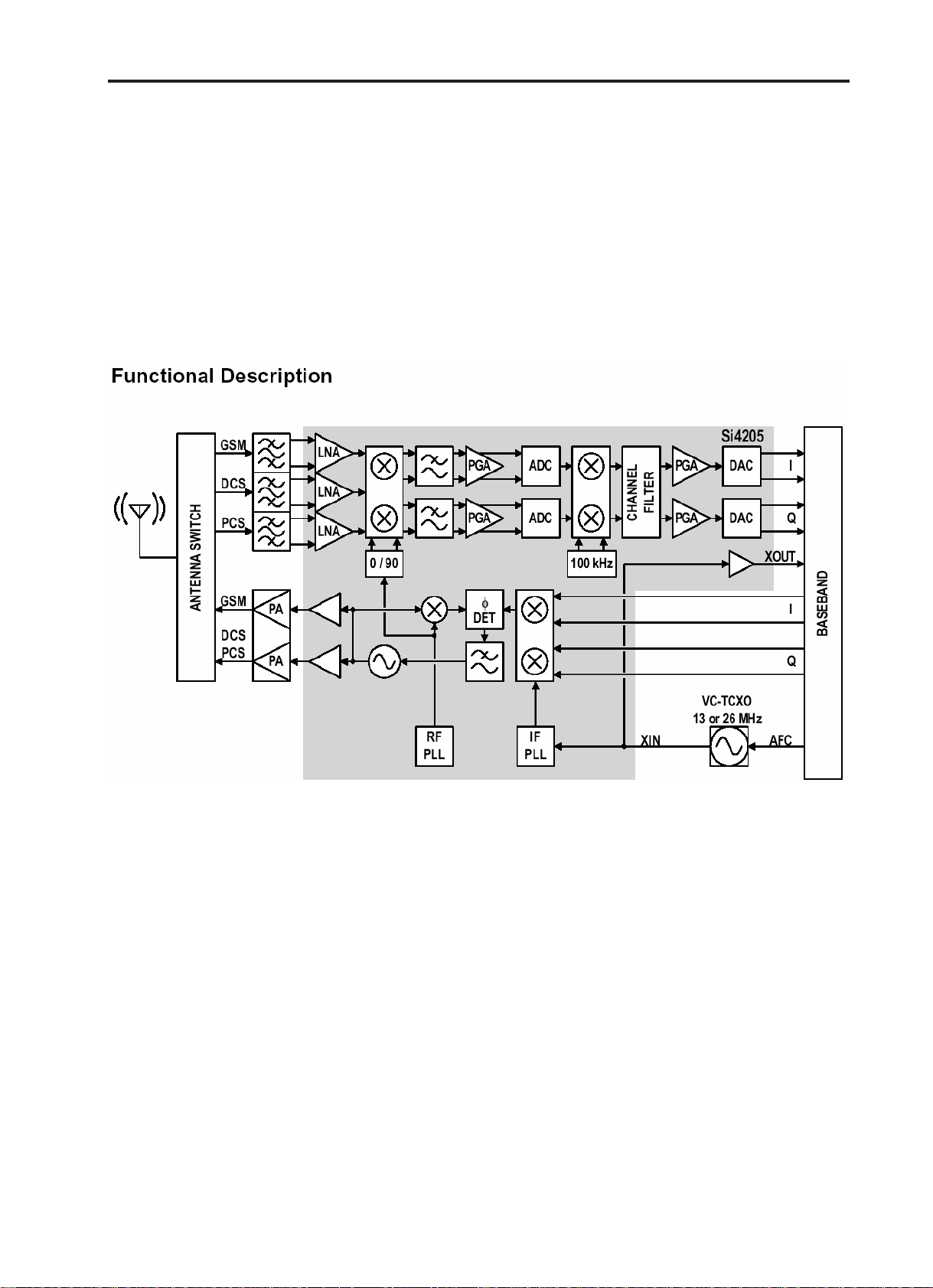
The Aero I transceiver is the integrated RF front end for multi-band GSM/GPRS digital cellular
handsets and wireless data modems. The integrated solution eliminates the IF SAW filter, external
low noise amplifier (LNAs) for three bands, transmit and RF voltage controlled oscillator (VCO
modules, and other discrete components found in conventional designs.
3. TECHNICAL BRIEF
Figure 3-1 Block Diagram of SI4205
(1) Receiver part
The Aero I transceiver uses a low-IF receiver architecture which allows for the on chip integration of
the channel selection filters, eliminating the external RF image reject filters and the IF SAW filter
required in conventional superheterodyne architectures.
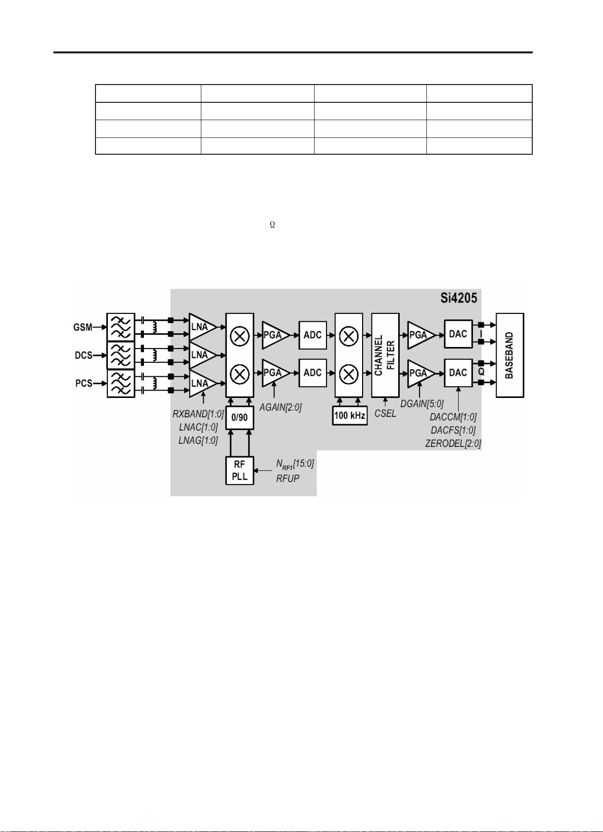
A. RF front end
RF front end consists of Antenna Switch(FL301), two SAW Filters(FL301, FL302) and dual band
LNAs integrated in transceiver (U301).
The Received RF signals(GSM 925MHz ~ 960MHz, DCS 1805MHz ~ 1880MHz) are fed into the
antenna or Mobile switch.
The Antenna Switch(FL301) is used to control the Rx and Tx paths. And, the input signals VC1 and
VC2 of a FL301 are directly connected to baseband controller to switch either Tx or Rx path on.
The logic and current is given below Table 3-1.
- 13 -
3. TECHNICAL BRIEF
GSM TX 0V 2.5 ~ 3.0V 10.0 mA max
DCS TX 2.5 ~ 3.0V 0V 10.0 mA max
GSM/DCS RX 0V 0V < 0.1 mA
Three differential-input LNAs are integrated in SI4205. The GSM input supports the GSM 850 (869849 MHz) or E-GSM 900 (925-960MHz) bands. The DCS input supports the DCS 1800 (1805-1880
MHz) band. The PCS input supports the PCS 1900 (1930-1990 MHz) band.
The LNA inputs are matched to the 150 balanced output SAW filters through external LC
matching networks. The LAN gain is controlled with the LANG[1:0] and LNAC[1:0] bits in register
05h (Figure 3-2)
VC1 VC2 Current
Table 3-1. The logic and current
Figure 3-2 Block Diagram of Receiver part of SI4205
B. Intermediate frequency (IF) and Demodulation
A quadrature image-reject mixer downconverts the RF signal to a 100KHz intermediate frequency
(IF) with the RFLO from the frequency synthesizer.
The RFLO frequency is between 1737.8 to 1989.9 MHz, and is internally divided by 2 for GSM 850
and E-GSM 900 modes. The mixer output is amplified with an analog programmable gain amplifier
(PGA), which is controlled with the AGAIN[2:0] bits in register 05h (Figure3-2). The quadrature IF
signal is digitized with high resolution A/D converters (ADCs).
The ADC output is downconverted to baseband with a digital 100KHz quadrature LO signal. Digital
decimation and IIR filters perform channel selection to remove blocking and reference interference
signals. The selectivity setting (CSEL=0) or a low selectivity setting (CSEL=1). The low selectivity
filter has a flatter group channelization filter is in the baseband chip. After channel selection, the
digital output is scaled with a digital PGA, which is controlled with the DGAIN [5:0] bits in register
05h.
The amplified digital output signal go through with DACs that drive a differential analog signal onto
the RXIP,RXIN,RXQP and RXQN pins to interface to standard analog ADC input baseband ICs. No
special processing is required in the baseband for offset compensation or extended dynamic range.
Compared to a direct-conversion architecture, the low-IF architecture has a much greater degree of
immunity to dc offsets that can arise from RF local
oscillator(RFLO) self-mixing, 2nd order distortion of blockers, and device 1/f noise.
- 14 -
3. TECHNICAL BRIEF
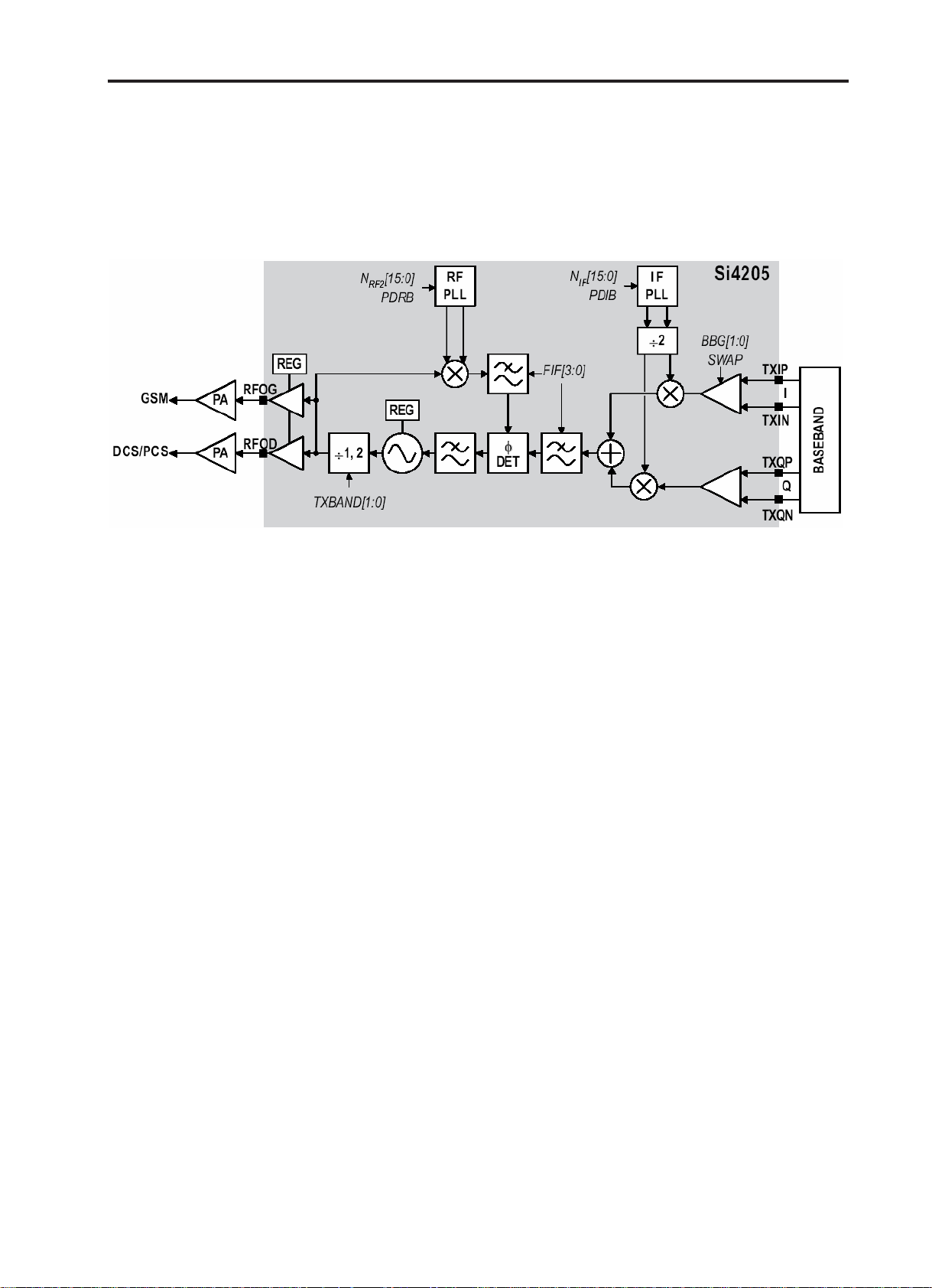
(2) Transmitter part
The transmit (Tx) section consists of an I/Q baseband upconverter, and offset phase-locked loop
(OPLL) and two output buffers that can drive external power amplifiers (PA), one for the GSM 850
(824-849 MHz) and E-GSM 900 (880-915 MHz) bands and one for the DCS 1800 (1710-1785 MHz)
and PCS 1900 (1850-1910MHz) bands.
Figure 3-3 Block Diagram of Transmitter part of SI4205
A. IF Modulator
The baseband converter(BBC) within the GSM chipset generates I and Q baseband signals for the
Transmit vector modulator. The modulator provides more than 40dBc of carrier and unwanted
sideband rejection and produces a GMSK modulated signal.
The baseband software is able to cancel out differential DC offsets in the I/Q baseband signals
caused by imperfections in the D/A converters.
The Tx-Modulator implements a quadrature modulator. A quadrature mixer upconverts the
differential in-phase (TXIP, TXIN) and quadrature (TXQP, TXQN) signals with the IFLO to generate
a SSB IF signal that is filtered and used as the reference input to the OPLL.
The IFLO frequency is generated between 766 and 896 MHz and internally divided by 2 to generate
the quadrature LO signals for the quadrature modulator, resulting in an IF between 383 and 448
MHz. For the E-GSM 900 band, two different IFLO frequencies are required for spur management.
Therefore, the IF PLL must be programmed per channel in the E-GSM 900 band.
B. OPLL
The OPLL consists of a feedback mixer, a phase detector, a loop filter, and a fully integrated
TXVCO. The TXVCO is centered between the DCS 1800 and PCS 1900 bands, and its output is
divided by 2 for the GSM 850 and E-GSM 900 bands. The RFLO frequency is generated between
1272 and 1483 MHz. To allow a single VCO to be used for the RFLO, high-side injection is used for
the GSM 850 and E-GSM 900 bands, and low-side injection is used for the DCS 1800 and PCS
1900 bands.
The I and Q signals are automatically swapped when switching bands. Additionally, the SWAP bit in
register 03h can be used to manually exchange the I and Q signals.
Low-pass filters before the OPLL phase detector reduce the harmonic content of the quadrature
modulator and feedback mixer outputs. The cutoff frequency of the filters is programmable with the
FIF[3:0] bits in register 04h (Figure 3-3), and should be set to the recommended settings detailed in
the register description.
- 15 -
3. TECHNICAL BRIEF
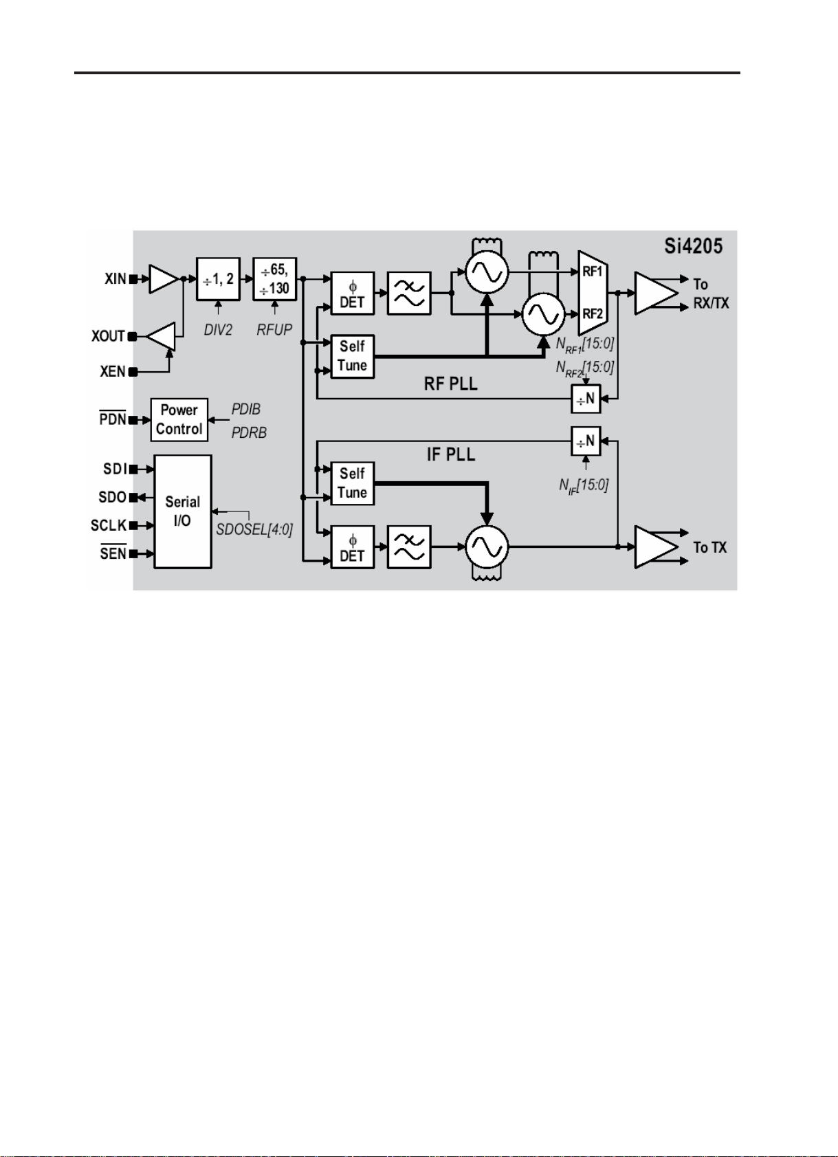
(3) Frequency Synthesizer
The transmit (Tx) section consists of an I/Q baseband upconverter, and offset phase-locked loop
(OPLL) and two output buffers that can drive external power amplifiers (PA), one for the GSM 850
(824-849 MHz) and E-GSM 900 (880-915 MHz) bands and one for the DCS 1800 (1710-1785 MHz)
and PCS 1900 (1850-1910MHz) bands.
Figure 3-4 Block Diagram of Frequency Synthesizer part of SI4205
The Aero I transceiver integrates two complete PLLs including VCOs, varactors, resonators, loop
filters, reference and VCO dividers, and phase detectors. The RF PLL uses two multiplexed VCOs.
The RF1 VCO is used for receive mode, and the RF2 VCO is used for transmit mode. The IF PLL is
used only during transmit mode.
All VCO tuning inductors are also integrated. The IF and RF output frequencies are set by
programming the N-Divider registers, N
RF1
, N
and NIF. Programming the N-Divider register for
RF2
either RF1 or RF2 automatically selects the proper VCO. The output frequency of each PLL is as
follows:
fout = N * fø
The DIV2 bit in register 31h controls a programmable divider at the XIN pin to allow either
a 13 or 26 MHz reference frequency. For receive mode, the RF1 PLL phase
detector update rate (fø) should be programmed fø= 100 kHz for DCS 1800 or PCS 1900 bands, and
fø= 200 kHz for GSM 850 and E-GSM 900 bands. For transmit mode, the RF2 and IF PLL phase
detector update rates are always fø=200 kHz.
- 16 -
3. TECHNICAL BRIEF
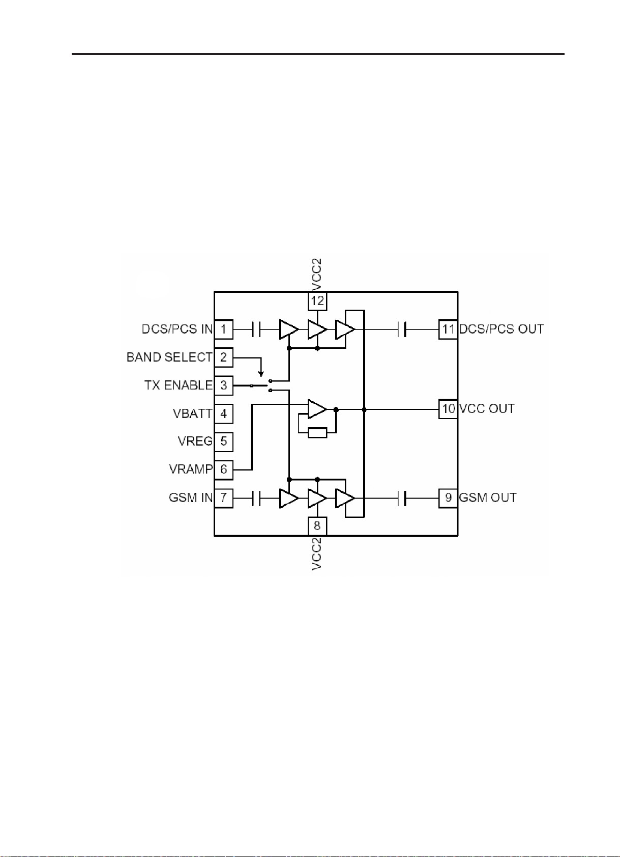
3.2 Power Amplifier Module (RF3133, U302)
TThe RF3133 is a high-power, high-efficiency power amplifier module with integrated power control.
The device is self-contained with 50input and output terminals. The power control function is also
incorporated, eliminating the need for directional couplers, detector diodes, power control ASICs
and other power control circuitry; this allows the module to be driven directly from the DAC output.
The device is designed for use as the final RF amplifier in GSM 850, E-GSM 900, DCS and PCS
handheld digital cellular equipment and other applications in the 824-849 MHz, 880-915 MHz, 17101785 MHz, and 1850-1910 MHz bands.
On-board power control provides over 37 dB of control range with an analog voltage input
(TX_RAMP); and, power down with a logic “low” for standby operation (TX_ENABLE).
External control (BAND_SELECT) is used to select the GSM or DCS band with a logic high or low.
A logic low enables the GSM band whereas a logic high enables the DCS band.
Figure 3-5 Functional Block Diagram of RF3133
- 17 -
3. TECHNICAL BRIEF
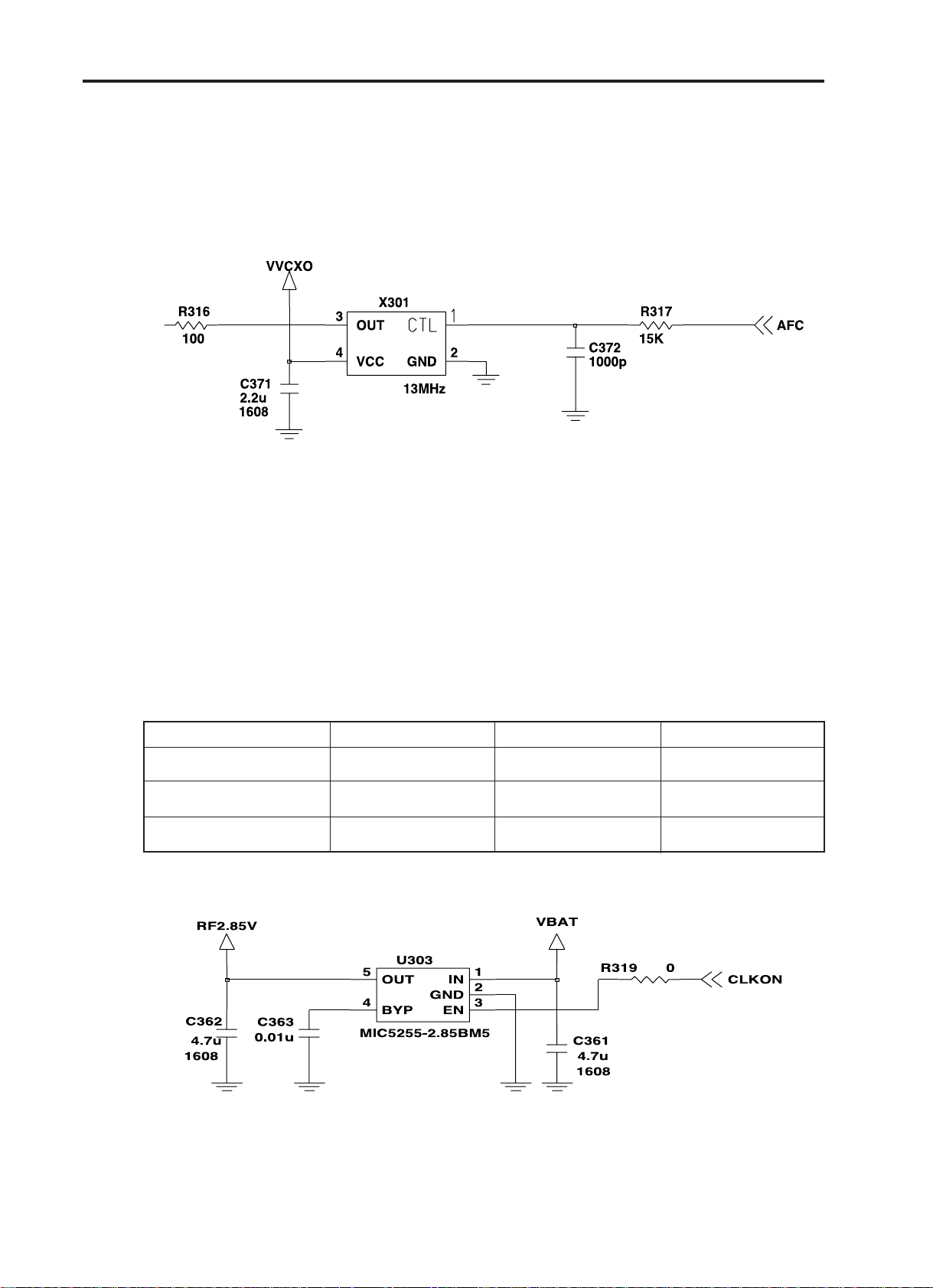
3.3 13 MHz Clock
The 13 MHz clock(X301) consists of a TCXO(Temperature Compensated Crystal Oscillator) which
oscillates at a frequency of 13 MHz. It is used within the Si4205, analog base band chipset (U101,
AD6537), digital base band chipset (U102, AD6525), and MIDI (U401) chipset.
Figure 3-6 VCTCXO circuit diagram
3.4 Power Supplies for RF Circuits
Two regulators are used for RF circuits. One is MIC5255 (U302), and the other is included of
AD6537B (U102).
MIC5255 (U303) supplies power to transceiver (SI4205, U301).
One port of AD6537B(U102) supplies power to VCTCXO (X301).
Main power (VBAT) from battery is used for PAM (RF3133, U302) because PAM requires high
power.
Table 3-2 Power suppliers for RF circuits.
Supplier Voltage Powers Enable Signal
U303 2.85V U301 CLKON
U102 2.75V X301
Battery 3.4~4.2V U302
Figure 3-7 U402 circuit diagram
- 18 -
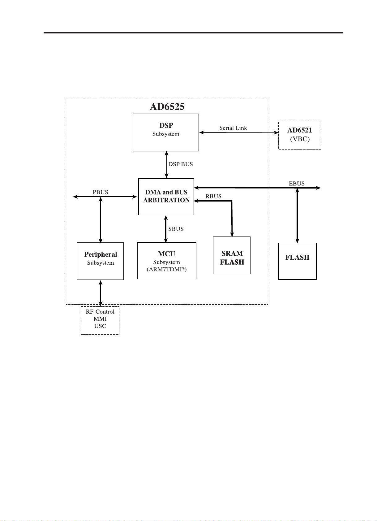
3.5 Digital Main Processor (AD6525, U101)
(1) Architecture Overview
3. TECHNICAL BRIEF
Figure 3-8 Block Diagram of the AD6525 Internal Architecture
The internal architecture of AD6525 is shown in Figure 3-8. AD6525 regroups three main
subsystems connected together through a dynamic and flexible communication bus network. It also
includes onboard system RAM (SRAM) and interfaces with external Flash Memory, Baseband
converter functions, and terminal functions like MMI, SIM and Universal System Connector
(USC).
The Digital Signal Processing (DSP) subsystem primarily hosts all the speech processing, channel
equalization and channel codec functions. The code used to implement such functions can be
stored in external Flash Memory and dynamically downloaded on demand into the DSP ’s program
RAM and Instruction Cache.
- 19 -

3. TECHNICAL BRIEF
The microcontroller subsystem supports all the GSM terminal software, including the layer 1, 2 and
3 of the GSM protocol stack, the MMI, and applications software such as data services, test and
maintenance. It is tightly associated with on-chip system SRAM and also includes boot ROM
memory with a small dedicated routine to facilitate the initialization of the external Flash Memory via
code download using the on-chip serial interface to the external Flash Memory interface.
The peripheral subsystem is composed of system peripherals such as interrupt controller, real time
clock, watch dog timer, power management and a timing and control module. It also includes
peripheral interfaces to the terminal functions: keyboard, battery supervision, radio and display. Both
the DSP and the MCU can access the peripheral subsystem via the peripheral bus (PBUS).
For program and data storage, both the MCU subsystem and the DSP subsystem can access the
on chip system SRAM and external memory such Flash Memory. The access to the SRAM module
is made through the RAM Bus (RBUS) under the control of the bus arbitration logic. Similarly,
access to the Flash Memory is through the parallel External Bus (EBUS).
- 20 -
3. TECHNICAL BRIEF
Figure 3-9 Example of System Interconnection of AD6525 External Interfaces
- 21 -
3. TECHNICAL BRIEF
(2) Interconnection with external devices
A. RTC Block Interface
Countered by external crystal oscillator (MC-146, X101).
The X-tal oscillates 32.768 KHz.
B. LCD Module Interface
Controlled by LCD_CS, LCD_RESET, ADD1, WR, DATA[0:15], VMEN, LCD_DIM, and LCD_ID.
Table 3-3 LCD module interface
LCD_CS LCD driver chip enable. LCD driver IC has own CS pin
LCD_RESET This pin resets LCD module.
This pin determines whether the data to LCD module are display data or
ADD1
control data. ADD1 can select 16 bit parallel bus. ADD1 is also used to
address flash memory.
Description
__WR Write control.
DATA [0:15] Parallel data lines. Color LCD driver chip uses the 16-bit data interface.
VMEM 3V voltage is supplied to white colored LED driver for backlighting.
LCD_DIM Control signal of white LED(LCD backlight) driver IC.
LCD_ID Reserved for future use.
C. RF Interface
The AD6525 control RF parts through RFEN, ANT_SW1/2, PA_EN, PA_BAND, RF_PWR_DWN,
S_EN, S_DATA, AND S_CLK.
Table 3-4 RF interface
GPO
4 RF_PWR_DWN Power Down Input
9 ANT_SW1 Antenna Switch Band Select
11 ANT_SW2 Antenna Switch Band Select
16 PA_EN PAM Enable / Disable
17 PA_BAND PAM Band Select
7 RFEN RF Enable / Disable
19 S_EN Serial Enable Input
20 S_DATA Serial Data Input
21 S_CLK Serial Clock Input
Signal
Name
Description
- 22 -

3. TECHNICAL BRIEF
D. SIM Interface
The AD6525 check status periodically in call mode if SIM card is inserted or not, but the
AD6525 don't check in deep sleep mode.
Interface signals are SIM-DATA, SIMCLK, SIM_RST
Table 3-3 LCD module interface
Description
SIM_DATA
SIMCLK Clock 3.25 MHz frequency.
SIM_RST Reset SIM Block.
This pin receives and sends data to SIM card. This model support
3.0 volt interface SIM card.
E. Key Interface
Key Interface includes 5 column (KEY_COL[0:4]) and 5 row (KEY_ROW[0:4]). AD6525
detects key press by interrupt.
- 23 -

3. TECHNICAL BRIEF
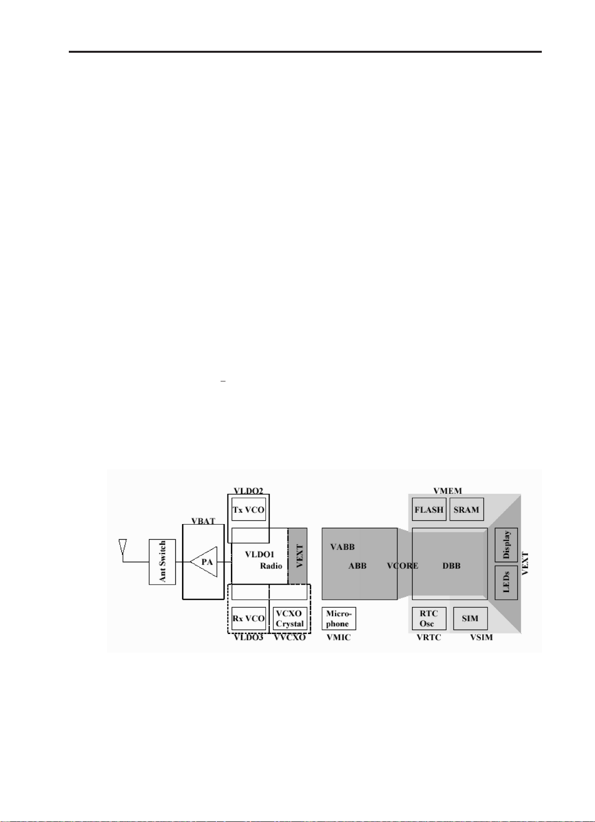
3.6 Power Supplies for RF Circuits
(1) Block Diagram
Figure 3-10 Functional Block Diagram of AD6537B
- 24 -
3. TECHNICAL BRIEF
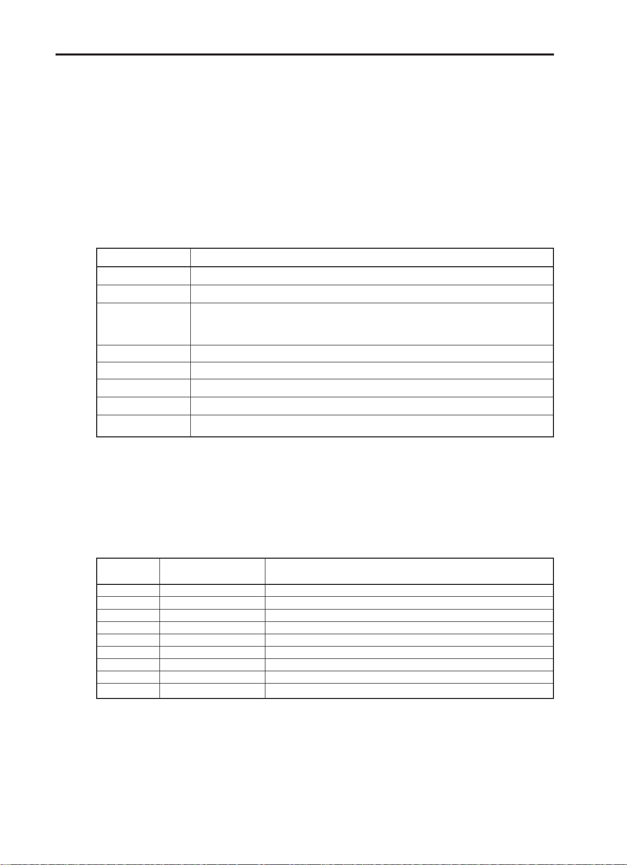
(2) BB Transmit Section
The AD6537 Baseband Transmit Section is designed to support GMSK for both single-slot and
multislot applications. The complete transmit path is shown below.
Figure 3-11 AD6537B Baseband Transmit Section
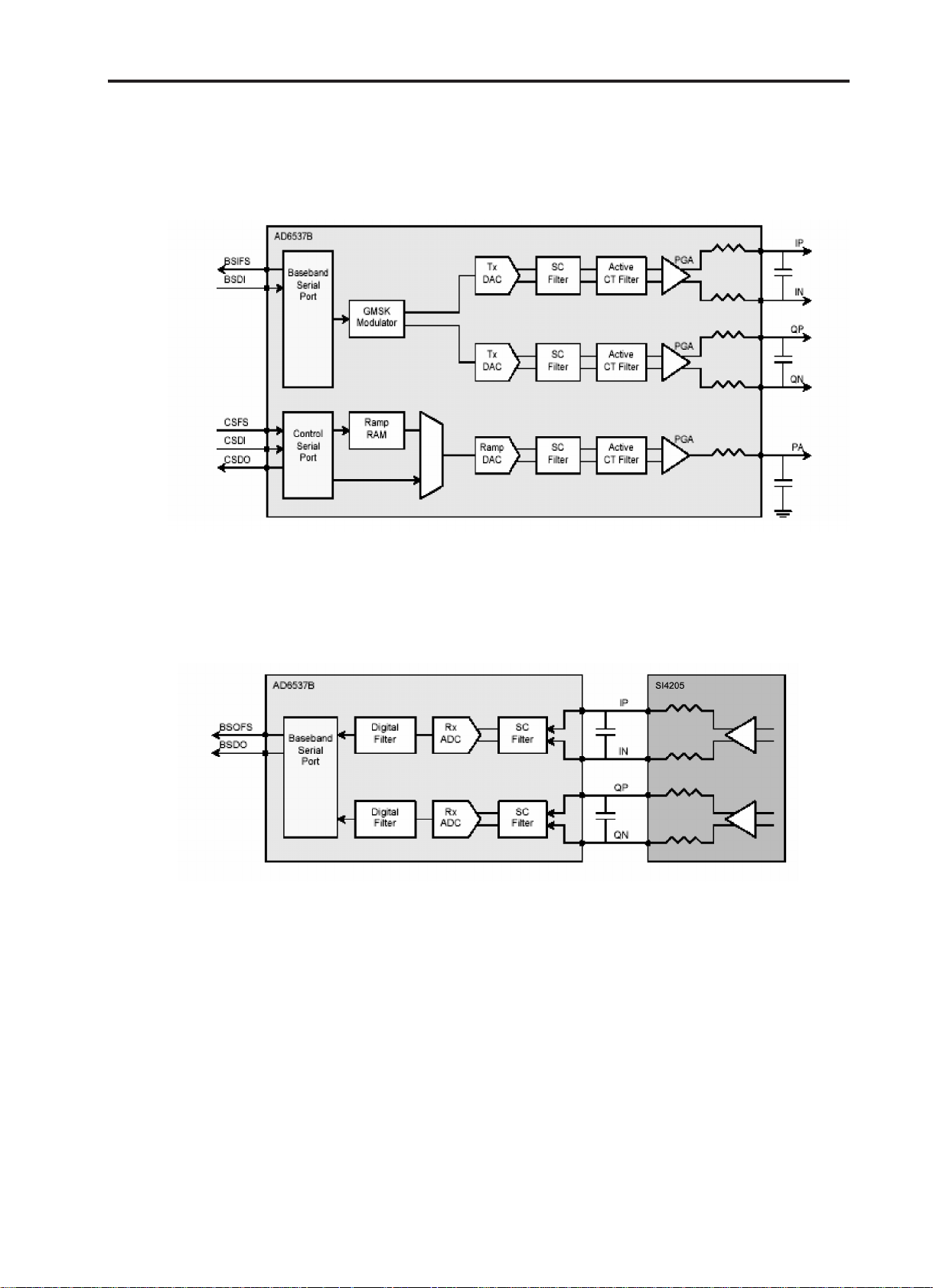
(3) BB Receive Section
The AD6537 Baseband Receive Section is designed to support GMSK applications
Figure 3-12 AD6537B Baseband Receiving Section
- 25 -

3. TECHNICAL BRIEF
(4) Auxiliary Section
The AD6537 Auxiliary Section includes an Automatic Frequency Control(AFC) DAC, internal
Bandgap reference voltage, voltage reference buffers, and an Auxiliary ADC.
Figure 3-13 AD6537B Auxiliary Section
- 26 -
3. TECHNICAL BRIEF
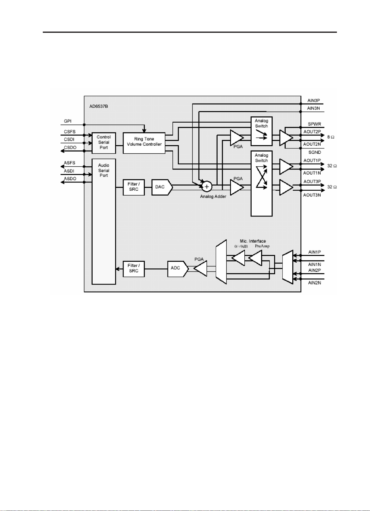
(5) Audio Section
The AD6537B Audio Section supports communications applications. The Audio Section provides an
audio codec with a digital-to-analog converter and an analog-to-digital converter, a ring tone volume
controller, a microphone interface, and multiple analog input and output channels.
Figure 3-14 AD6537B Audio Section
- Main Mic Interface uses a differential configuration with AIN1P & AIN1N.
- Main Receiver Interface uses a differential configuration with AOUT1P & AOUT1N.
- Headset Mic Interface uses a single-ended configuration with AIN2P & AIN2N.
- Headset Receiver Interface uses a single-ended configuration with AOUT3P & AOUT3N.
- 27 -
3. TECHNICAL BRIEF
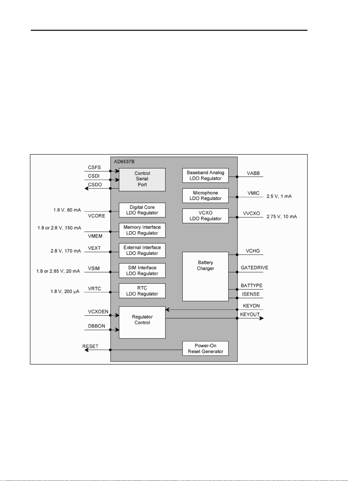
(6) Power Management Section
The voltage regulators are enabled based on the status of the battery and input from the user or
software. If the AD6537B is in Deep Discharge Lockout(DDLO) or Under-Voltage Lockout(UVLO)
only the Real-Time Clock regulator is active. If the AD6537 is in Thermal Shutdown only the RealTime Clock regulator is active.
If the battery is not in Deep Discharge Lockout, Under-Voltage Lockout, or Thermal Shutdown, the
Real-Time Clock regulator is always enabled and the other regulators are enabled based on input
from the user or software. If the user presses the power-on key(KEYON), the regulators required to
boot the software are enabled. If a charger is detected(CHGDET) the regulators required to boot the
software are enabled. If the software asserts the DBBON signal the regulators required to maintain
the software state are enabled. The VCXOEN signal enables the VCXO regulator and optional
external DC/DC converter(LDOEN). Writing through the CSPORT enables the analog regulators.
Figure 3-15 AD6537B Power Management Section
- 28 -
3. TECHNICAL BRIEF
Power on sequence
If a battery is inserted, the battery powers the 8 LDOs.
Then if PWR KEY is detected, the LDOs output turn on.
REFOUT is also enabled, Reset signal is generated and send to the AD6525.
Charging Process
1. Check charger is inserted or not.
2. If AD6537B detects that Charger is inserted, the CC-CV charging starts.
3. Exception: When battery voltage is lower than 3.2V, the trickle charge (low current charge mode)
starts firstly. After the battery voltage reaches to 3.2V, the CC-CV charging starts.
Battery charging block
It can be used to charge Lithium Ion and/or Nickel Metal Hydride batteries. The phones use Li-Ion
battery only. Charger initialization, trickle charging, and constant current charging are implemented
in hardware.
Pins used for charging
CHGDET : Interrupt to AD6525 when charger is plugged.
BATDET : Interrupt to AD6525 when battery was detected.
REFCHG : Reference Voltage signal(1.2V), in order to detect phone temperature.
TA (Travel Adaptor)
Input voltage : AC 110V ~ 240V, 50~60Hz
Output voltage : DC 5.2V(+0.2 V)
Output current : Max 800mA
Battery
Li-ion battery : Max 4.2V, Nom 3.7V
Standard battery : Capacity - 780mAh, Li-ion
Figure 3-16 LDOs of AD6537B
- 29 -
3. TECHNICAL BRIEF
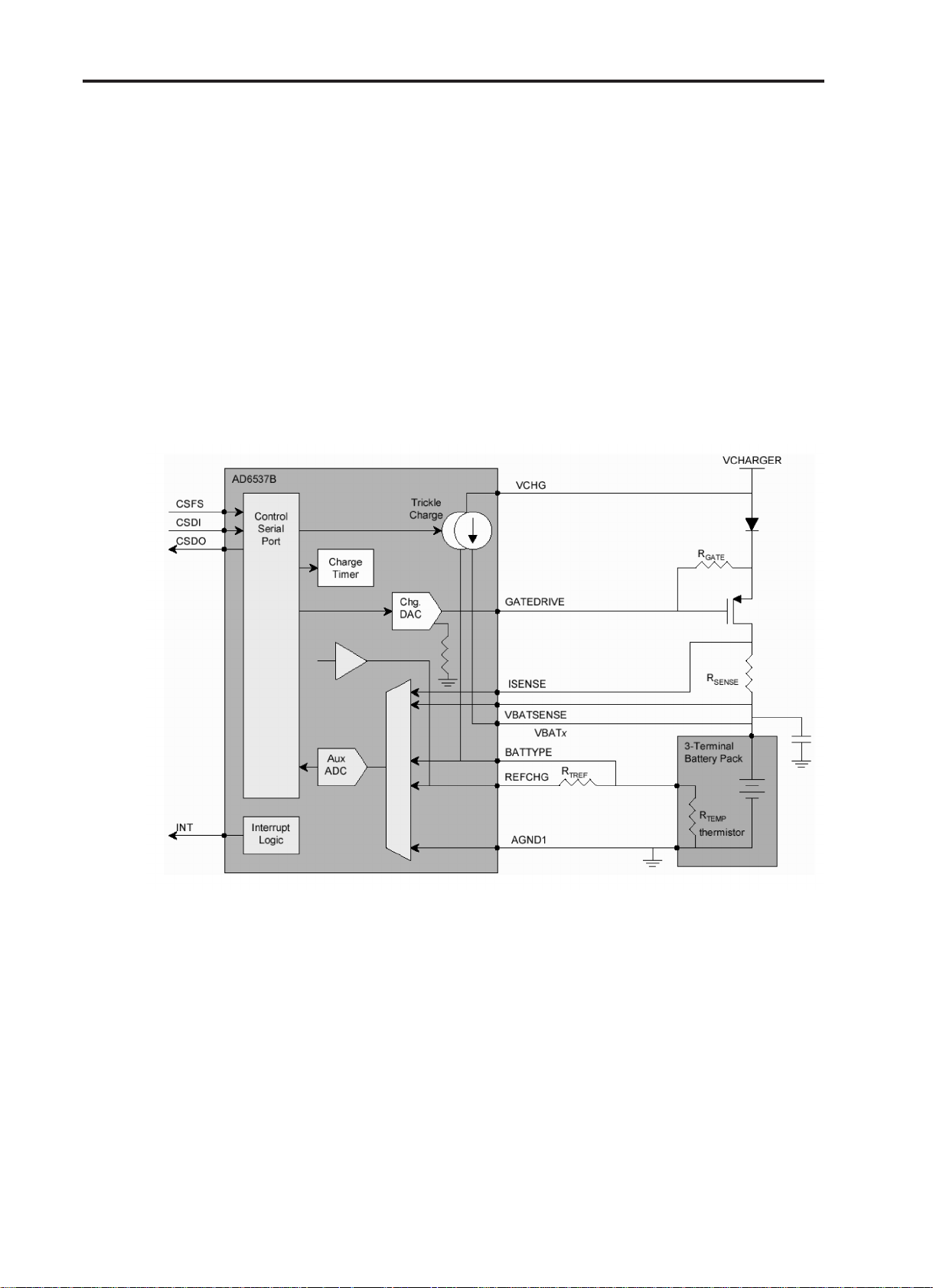
(7) Battery Charging
The AD6573B battery charger can be used with Lithium-lon(Li+) and Nickel-Metal-Hydride (NiMH)
batteries.
The charger circuitry consists of a number of on-chip blocks and a few external components. The
on-chip charger circuitry includes the Trickle Charge block, the charge DAC, the Charge Timer, the
Interrupt Logic, the Auxiliary ADC, four interfaces to the Auxiliary ADC(current sense, battery
voltage, battery type and temperature), the control serial port(CSPORT).
If the charger supply voltage is limited to less than 5.25V(VCHG<5.25 V) the only external devices
required are: a power MOSFET pass device, a resistor to convert the Charge DAC output current to
a gate voltage, a diode to prevent current from flowing from the battery to the charger detect input, a
current sense resistor, a resistor to set the full-scale output current of the Charge DAC and a
capacitor to set the frequency of the Charge Timer oscillator. Optionally, a bipolar pass device may
be used in place of the MOSFET pass device/resistor combination.
Figure 3-17 Battery Charger for 3-Terminal Battery Pack
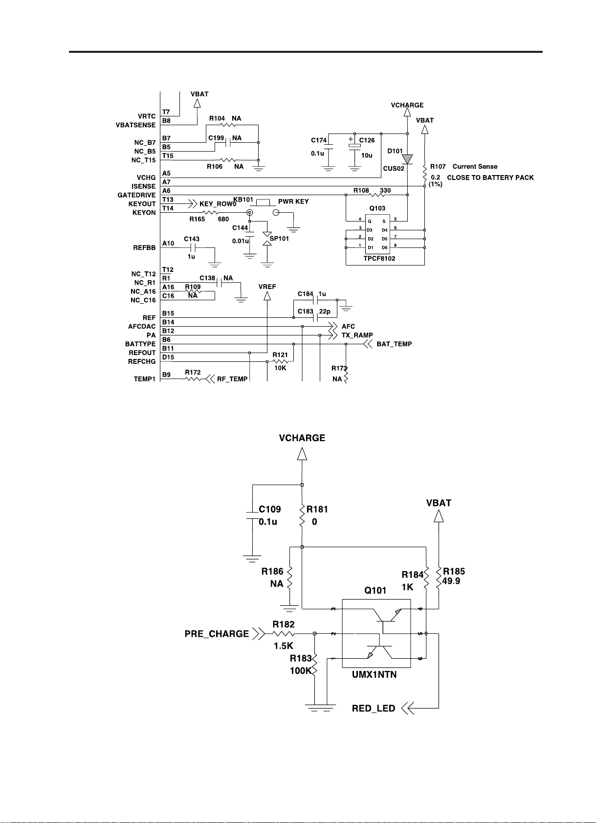
In order to reduce time for trickle charging, additional circuit(Pre-charge circuit)
was included. This circuit has supplied a 50mA current into the battery additionally.
So call it, it reduce trickle charging time
- 30 -
3. TECHNICAL BRIEF
Figure 3-18 Circuit Diagram of AD6537B(charging part)
Figure 3-19 Pre-charge Circuit
- 31 -
 Loading...