

LG RH7521W, 7926W, 7823W, RH7823W, RH7926W Service Manual

HDD/DVD RECORDER
SERVICE MANUAL
MODEL : RH7521W/7823W/7926W
MODEL : RH7521W/7823W/7926WSERVICE MANUAL
P/NO : 3829RHP042G
APRIL, 2005
Printed in Korea
CAUTION
BEFORE SERVICING THE UNIT, READ THE “SAFETY PRECAUTIONS”
IN THIS MANUAL.

CONTENTS
SECTION 1 . . . .SUMMARY
SECTION 2 . . . .CABINET & MAIN CHASSIS
SECTION 3 . . . .ELECTRICAL
SECTION 4 . . . .RL-05 LOADER PART
SECTION 5 . . . .REPLACEMENT PARTS LIST

1-2
SECTION 1
SUMMARY
CONTENTS
NEW FUNCTIONS OF HDD/DVD-RECORDER................................................................. 1-2
PRODUCT SAFETY SERVICING GUIDELINES FOR VIDEO PRODUCTS.............. 1-3
SERVICING PRECAUTIONS .................................................................................................. 1-4
• General Servicing Precautions
• Insulation Checking Prodedure
• Electrostatically Sensitive Devices
SERVICE INFORMATION FOR EEPROM IC SETTING ................................................. 1-5
SPECIFICATIONS ...................................................................................................................... 1-6

1-3
NEW FUNCTIONS OF HDD/DVD-RECORDER
• HDMI
HDMI IS THE SPECIFICATION FOR THE HIGH-DEFINITION MULTIMEDIA INTERFACE. HDMI IS PROVIDED FOR TRANSMITTING DIGITAL TELEVISION AUDIOVISUAL SIGNALS FROM HDD-DVD RECORDER TO
TELEVISION SETS, OTHER VIDEO DISPLAYS. HDMI CAN CARRY HIGH QUALITY MULTI-CHANNEL
AUDIO DATA AND CAN CARRY ALL STANDARD AND HIGH DEFINITION CONSUMER ELECTRONICS
VIDEO FORMATS. CONTENT PROTECTION TECHNOLOGY IS AVAILABLE. HDMI CAN ALSO CARRY
CONTROL AND STATUS INFORMATION IN BOTH DIRECTIONS.
<< OPERATING >>
AUDIO, VIDEO AND AUXILIARY DATA IS TRANSMITTED ACROSS THE THREE TMDS DATA CHANNELS.
THE VIDEO PIXEL CLOCK IS TRANSMITTED ON THE TMDS CLOCK CHANNEL AND IS USED BY THE
RECEIVER AS A FREQUENCY REFERENCE FOR DATA RECOVERY ON THE THREE TMDS DATA CHANNELS.
VIDEO DATA IS CARRIED AS A SERIES OF 24-BIT PIXELS ON THE THREE TMDS DATA CHANNELS.
TMDS ENCODING CONVERTS THE 8BIT PER CHANNEL INTO THE 10BIT DC–BALANCED.
VIDEO PIXEL RATES CAN RANGE FROM 25MHZ TO 165MHZ. THE VIDEO PIXELS CAN BE ENCODED IN
EITHER RGB,YCBCR 4:4:4 OR YCBCR 4:2:2 FORMATS. IN ALL THREE CASES, UP TP 24 BITS PER
PIXEL CAN BE TRANSFERRED.
FAST DUBBING
DUBBING MEANS A COPYING FUNCTION BETWEEN HDD TO DVD DISCS.
COPYING BETWEEN HDD TO DVD IS A COMPLETELY DIGITAL PROCESS AND THEREFORE INVOLVES
NO LOSS OF QUALITY IN THE AUDIO OR VIDEO. SO THIS MEANS THAT COPYING CAN BE CARRIED
OUT AT THE MAXIMUM SPEED POSSIBLE.
<< DUBBING SPEED RATE >>
NORMAL DUBBING : SPEED RATE MAX X1
FAST DUBBING : SPEED RATE MAX X4
WHEN FAST DUBBING FROM HDD TO DVD , THE SPEED OF COPYING DEPENDS ON THE RECORDING
MODE AND THE KIND OF USING THE DVD DISC, AND THIS MODE IS NOT AVAILABLE FOR EDITED
VIDEO TITLE IN HDD.
WHEN FAST DUBBING FROM DVD TO HDD , ONLY AVAILABLE WHEN COPYING VR MODE DISC(DVD-
RW) TO HDD , AND ONLY NORMAL DUBBING AVAILABLE WHEN COPYING VIDEO MODE DISC
(DVD+R/RW, DVD-R) TO HDD
1-4
IMPORTANT SAFETY NOTICE
This manual was prepared for use only by properly trained audio-video service
technicians.
When servicing this product, under no circumstances should the original
design be modified or altered without permission from LG Electronics
Corporation. All components should be replaced only with types identical to
those in the original circuit and their physical location, wiring and lead dress
must conform to original layout upon completion of repairs.
Special components are also used to prevent x-radiation, shock and fire hazard. These components are indicated by the letter “x” included in their component designators and are required to maintain safe performance. No deviations
are allowed without prior approval by LG Electronics Corporation.
Circuit diagrams may occasionally differ from the actual circuit used. This way,
implementation of the latest safety and performance improvement changes
into the set is not delayed until the new service literature is printed.
CAUTION: Do not attempt to modify this product in any way. Never perform
customized installations without manufacturer’s approval. Unauthorized modifications will not only void the warranty, but may lead to property damage or
user injury.
Service work should be performed only after you are thoroughly familiar with
these safety checks and servicing guidelines.
GRAPHIC SYMBOLS
The exclamation point within an equilateral triangle is intended to
alert the service personnel to important safety information in the
service literature.
The lightning flash with arrowhead symbol within an equilateral triangle is intended to alert the service personnel to the presence of
noninsulated “dangerous voltage” that may be of sufficient magnitude to constitute a risk of electric shock.
The pictorial representation of a fuse and its rating within an equilateral triangle is intended to convey to the service personnel the
following fuse replacement caution notice:
CAUTION: FOR CONTINUED PROTECTION AGAINST RISK
OF FIRE, REPLACE ALL FUSES WITH THE SAME TYPE AND
RATING AS MARKED NEAR EACH FUSE.
SERVICE INFORMATION
While servicing, use an isolation transformer for protection from AC line shock.
After the original service problem has been corrected, make a check of the following:
FIRE AND SHOCK HAZARD
1. Be sure that all components are positioned to avoid a possibility of adjacent
component shorts. This is especially important on items trans-ported to and
from the repair shop.
2. Verify that all protective devices such as insulators, barriers, covers, shields,
strain reliefs, power supply cords, and other hardware have been reinstalled
per the original design. Be sure that the safety purpose of the polarized line
plug has not been defeated.
3. Soldering must be inspected to discover possible cold solder joints, solder
splashes, or sharp solder points. Be certain to remove all loose foreign particles.
4. Check for physical evidence of damage or deterioration to parts and components, for frayed leads or damaged insulation (including the AC cord), and
replace if necessary.
5. No lead or component should touch a high current device or a resistor rated
at 1 watt or more. Lead tension around protruding metal surfaces must be
avoided.
6. After reassembly of the set, always perform an AC leakage test on all
exposed metallic parts of the cabinet (the channel selector knobs, antenna
terminals, handle and screws) to be sure that set is safe to operate without
danger of electrical shock. DO NOT USE A LINE ISOLATION TRANSFORMER DURING THIS TEST. Use an AC voltmeter having 5000 ohms per
volt or more sensitivity in the following manner: Connect a 1500 ohm, 10
watt resistor, paralleled by a .15 mfd 150V AC type capacitor between a
known good earth ground water pipe, conduit, etc.) and the exposed metallic parts, one at a time. Measure the AC voltage across the combination of
1500 ohm resistor and .15 mfd capacitor. Reverse the AC plug by using a
non-polarized adaptor and repeat AC voltage measurements for each
exposed metallic part. Voltage measured must not exceed 0.75 volts RMS.
This corresponds to 0.5 milliamp AC. Any value exceeding this limit constitutes a potential shock hazard and must be corrected immediately.
TIPS ON PROPER INSTALLATION
1. Never install any receiver in a closed-in recess, cubbyhole, or closely fitting
shelf space over, or close to, a heat duct, or in the path of heated air flow.
2. Avoid conditions of high humidity such as: outdoor patio installations where
dew is a factor, near steam radiators where steam leakage is a factor, etc.
3. Avoid placement where draperies may obstruct venting. The customer
should also avoid the use of decorative scarves or other coverings that
might obstruct ventilation.
4. Wall- and shelf-mounted installations using a commercial mounting kit must
follow the factory-approved mounting instructions. A product mounted to a
shelf or platform must retain its original feet (or the equivalent thickness in
spacers) to provide adequate air flow across the bottom. Bolts or screws
used for fasteners must not touch any parts or wiring. Perform leakage tests
on customized installations.
5. Caution customers against mounting a product on a sloping shelf or in a tilted position, unless the receiver is properly secured.
6. A product on a roll-about cart should be stable in its mounting to the cart.
Caution the customer on the hazards of trying to roll a cart with small casters across thresholds or deep pile carpets.
7. Caution customers against using extension cords. Explain that a forest of
extensions, sprouting from a single outlet, can lead to disastrous consequences to home and family.
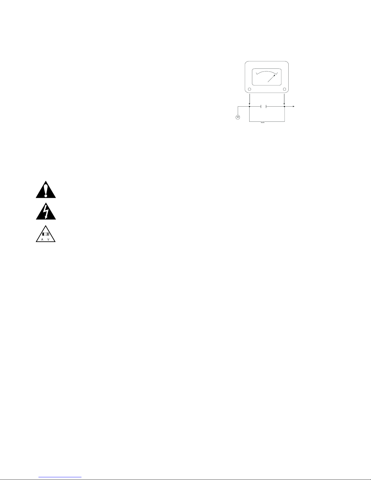
A.C. Voltmeter
1500 OHM
10 WATT
Place this probe
on each exposed
metal part.
Good Earth Ground
such as the Water
Pipe, Conduit, etc.
0.15uF
PRODUCT SAFETY SERVICING GUIDELINES FOR VIDEO PRODUCTS

1-5
SERVICING PRECAUTIONS
CAUTION : Before servicing the HDD/DVD Recorder covered by this service data and its supplements and addends,
read and follow the
SAFETY PRECAUTIONS. NOTE : if
unforeseen circumstances create conflict between the following servicing precautions and any of the safety precautions in this publications, always follow the safety precautions.
Remembers Safety First:
General Servicing Precautions
1. Always unplug the HDD/DVD Recorder AC power cord
from the AC power source before:
(1) Removing or reinstalling any component, circuit board,
module, or any other assembly.
(2) Disconnection or reconnecting any internal electrical
plug or other electrical connection.
(3) Connecting a test substitute in parallel with an elec-
trolytic capacitor.
Caution : A wrong part substitution or incorrect
polarity installation of electrolytic capacitors may result
in an explosion hazard.
2. Do not spray chemicals on or near this HDD/DVD
Recorder or any of its assemblies.
3. Unless specified otherwise in this service data, clean
electrical contacts by applying an appropriate contact
cleaning solution to the contacts with a pipe cleaner,
cotton-tipped swab, or comparable soft applicator.
Unless specified otherwise in this service data, lubrication
of contacts is not required.
4. Do not defeat any plug/socket B+ voltage interlocks with
whitch instruments covered by this service manual might
be equipped.
5. Do not apply AC power to this HDD/DVD Recorder and/or
any of its electrical assemblies unless all solid-state
device heat sinks are cerrectly installed.
6. Always connect test instrument ground lead to the
appropriate ground before connection the test instrument
positive lead. Always remove the test instrument ground
lead last.
Insulation Checking Procedure
Disconnect the attachment plug from the AC outlet and turn
the power on. Connect an insulation resistance meter(500V)
to the blades of the attachment plug. The insulation resistance between each blade of the attachment plug and accessible conductive parts (Note 1) should be more than 1Mohm.
Note 1 : Accessible Conductive Parts including Metal panels, Input terminals, Earphone jacks, etc.
Electrostatically Sensitive (ES) Devices
Some semiconductor (solid state) devices can be damaged
easily by static electricity. Such components commonly are
called Electrostatically Sensitive (ES) Devices. Examples of
typical ES devices are integrated circuits and some field
effect transistors and semiconductor chip components.
The following techniques should be used to help reduce the
incidence of component damage caused by static electricity.
1. Immediately before handling any semiconductor component or semiconductor-equipped assembly, drain off any
electrostatic charge on your body by touching a known
earth ground. Alternatively, obtain and wear a commercially available discharging wrist strap device, which
should be removed for potential shock reasons prior to
applying power to the unit under test.
2. After removing an electrical assembly equipped with ES
devices, place the assembly on a conductive surface such
as aluminum foil, to prevent electrostatic charge buildup or
exposure of the assembly.
3. Use only a grouned-tip soldering iron to solder or unsolder
ES devices.
4. Use only an anti-static solder removal device. Some
solder removal devices not classified a “anti-static” can
generate electrical charges sufficient to damage ES
devices.
5. Do not use freon-propelled chemicals. These can
generate electrical charge sufficient to damage ES
devices.
6. Do not remove a replacement ES device from its protec
tive package until immediately before you are ready to
install it. (Most replacement ES devices are packaged with
leads electrically shorted together by conductive foam,
aluminum foil, or comparable conductive material).
7. Immediately before removing the protective material from
the leads of a replacement ES device, touch the protective
material to the chassis or circuit assembly into which the
device will be installed.
Caution : Be sure no power is applied to the chassis or
circuit, and observe all other safety precautions.
8. Minimize bodily motions when handling unpackaged
replacement ES devices. (Normally harmless motion such
as the brushing together of your clothes fabric or the lifting
of your foot from a carpeted floor can generate static electricity sufficient to damage an ES device.)
1-6
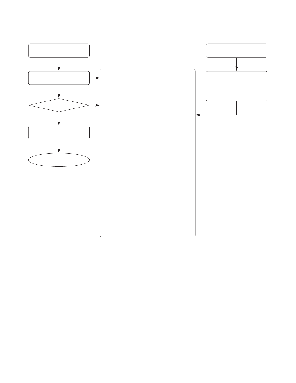
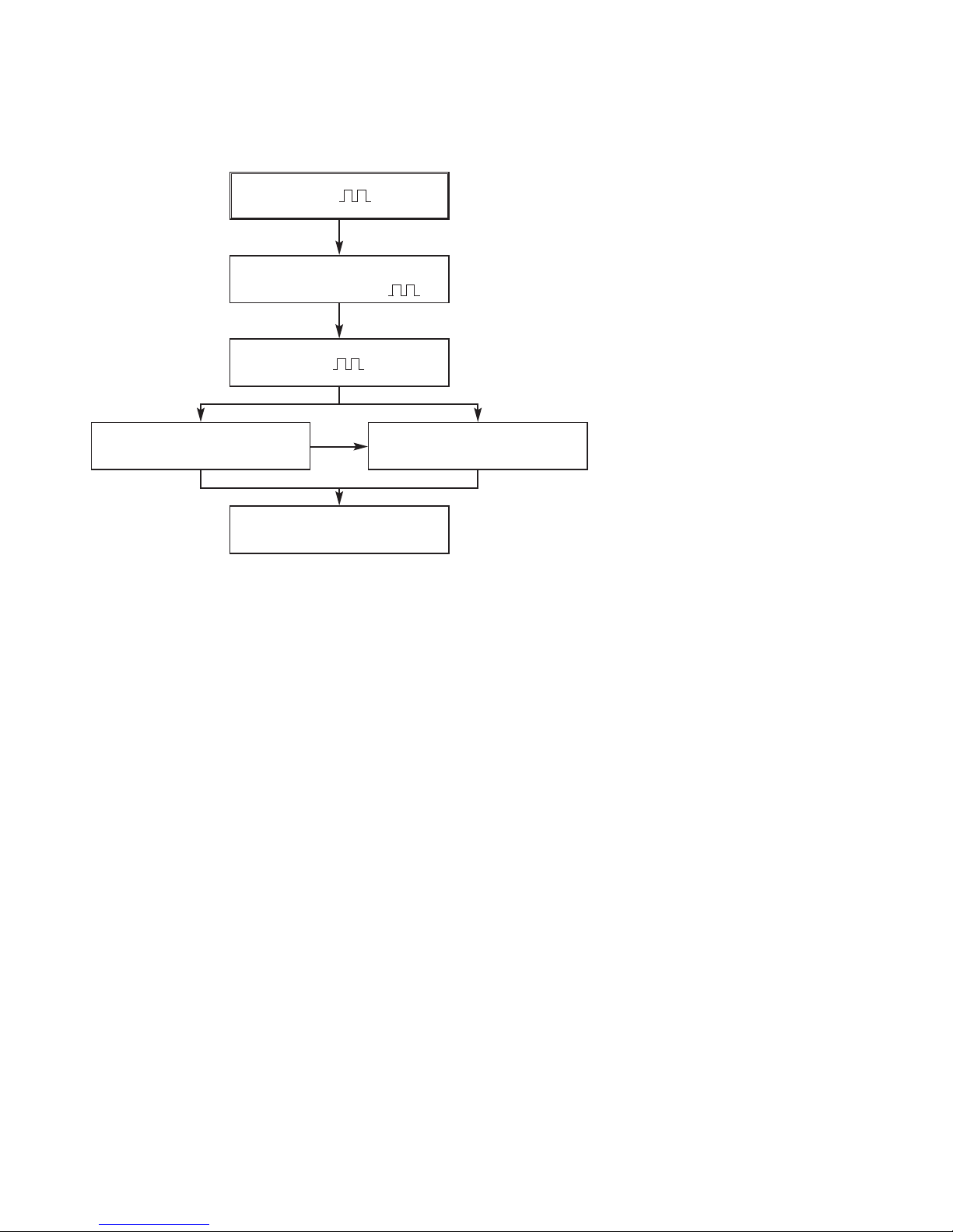
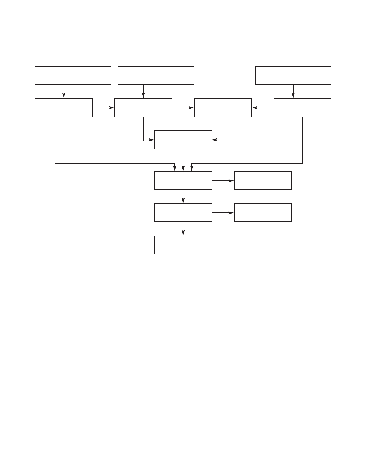
SERVICE INFORMATION FOR EEPROM IC SETTING
MICOM START
EEPROM ID CHECK
2 BYTE(B3,248,249)
MODEL NAME HEX BINARY
RH7521W OPT104 00000000
OPT2 00 00000000
OPT3 05 00000000
OPT4 10 00000000 (reserved)
OPT5 5B 00000000 (reserved)
OPT6 CC 00000000 (reserved)
OPT7 01 00000000 (reserved)
OPT8 15 00000000 (reserved)
RH7823W OPT10400000000
OPT2 2000000000
OPT3 05 00000000
OPT4 2000000000 (reserved)
OPT5 5B 00000000 (reserved)
OPT6 CC 00000000 (reserved)
OPT7 01 00000000 (reserved)
OPT8 15 00000000 (reserved)
RH7926W OPT10400000000
OPT2 2000000000
OPT3 05 00000000
OPT4 3000000000 (reserved)
OPT5 5B 00000000 (reserved)
OPT6 CE 00000000 (reserved)
OPT7 01 00000000 (reserved)
OPT8 15 00000000 (reserved)
WRITE:OK EXIT:MENU,MP
MOVE:< > EDIT : __
OPTION WRITE : OK (OK KEY IN)
MASK : R00 , EEP : R00 , (D10)
(Each mask ,eeprom, It shows a development
release version.)
DETECT NEW EEPROM (OPTION EDIT SCREEN)
*** EEPROM INITIAL ***
- SETUP is displayed in the field if pressing the Front ch- & ch+ Key with the Remocon number "clear"
key pressed in the status of powering on.
- AUTO SEARCH is done since the initial screen of ACMS is serviced if powering on.
OPTION DATA READ
5TIME & COMPARE
MICOM NORMAL
OPERATION START
Press the "CLEAR" key on the
Remote controller and the "CH - "
key one the Front Panel the same
time, then it goes in to Tracking
initial mode.
OPTION CONFIRMATION MODE
ID OK?
No
No
Yes
Yes
Yes

1-7
SPECIFICATIONS
• GENERAL
Power requirements AC 100-240V, 50/60 Hz
Power consumption 45W
Dimensions (approx.) 430 X 49 X 350 mm (w x h x d) without foot
Mass (approx.) 4.6 kg
Operating temperature 5°C to 35°C
Operating humidity 5 % to 90 %
Signal system PAL
• RECORDING
Recording format DVD Video Recording, DVD-VIDEO
Recordable media HDD (250GB), DVD-ReWritable, DVD-Recordable, DVD+ReWritable,
DVD+Recordable, DVD+Recordable (Double Layer)
Recordable time DVD (4.7GB): Approx. 1 hour (HQ mode), 2 hours (SQ mode),
4 hours (LQ mode), 6 hours (EQ mode)
DVD+R DL (8.5GB): Approx. 3 hour (HQ mode),
3 hours 40 minutes (SQ mode),
7 hours 10 minutes (LQ mode),
10 hours 30 minutes (EQ mode)
HDD (250GB): Approx. 66 hours 30 minutes (HQ mode),
129 hours (SQ mode), 239 hours (LQ mode),
356 hours (EQ mode)
Video recording format
Sampling frequency 27MHz
Compression format MPEG 2 (VBR support)
Audio recording format
Sampling frequency 48kHz
Compression format Dolby Digital
• PLAYBACK
Frequency response DVD (PCM 48 kHz): 8 Hz to 20 kHz, CD: 8 Hz to 20 kHz
DVD (PCM 96 kHz): 8 Hz to 44 kHz
Signal-to-noise ratio More than 100 dB (AUDIO OUT connector)
Harmonic distortion Less than 0.008% (AUDIO OUT connector)
Dynamic range More than 95 dB (AUDIO OUT connector)
• INPUTS
ANTENNA IN Antenna or CATV input, 75 ohms
VIDEO IN 1.0 Vp-p 75 ohms, sync negative, RCA jack x 2
S-VIDEO IN (Y) 1.0 V (p-p), 75 Ω, negative sync, Mini DIN 4-pin x 1
(C) 0.286 V (p-p) 75 Ω
AUDIO IN 0 dBm more than 47 kohms, RCA jack (L, R) x 2
DV IN 4 pin (IEEE 1394 standard)
• OUTPUTS
VIDEO OUT 1 Vp-p 75 Ω, sync negative, RCA jack x 1
S-VIDEO OUT (Y) 1.0 V (p-p), 75 Ω, negative sync, Mini DIN 4-pin x 1
(C) 0.286 V (p-p) 75 Ω
COMPONENT VIDEO OUT (Y) 1.0 V (p-p), 75 Ω, negative sync, RCA jack x 1
(PROGRESSIVE SCAN) (Pb)/(Pr) 0.7 V (p-p), 75 Ω, RCA jack x 2
Audio output (digital audio) 0.5 V (p-p), 75 Ω, RCA jack x 1
Audio output (optical audio) 3 V (p-p), 75 Ω, Optical connector x 1
Audio output (analog audio) 2.0 Vrms (1 KHz, 0 dB), 600 Ω, RCA jack (L, R) x 1
RF OUT Channel 3 or 4 (Switchable)

2-1
SECTION 2
CABINET & MAIN CHASSIS
CONTENTS
EXPLODED VIEWS ....................................................................................................................2-2
1. Cabinet and Main Frame Section ..........................................................................................2-2
2. Deck Mechanism Section(RL-05S) ........................................................................................2-3
3. Packing Accessory Section ...................................................................................................2-4
2-2
EXPLODED VIEWS
1. Cabinet and Main Frame Section
265
260
A44
300
A47
468
273
104
101
100
102
103
102
102
102
103
103
103
410
410
457
274
283
A48
463
A54
457
A60
A53
A26
A43
A50
280
275
275
275
452
452
272
463
463
463
A46
250
463
463
463
261
261
320
465
261
26
8
468
270
468
468
468
A52
468
267
467
OPTIONAL PART
A
5
4
3
2
1
BCD
2-3
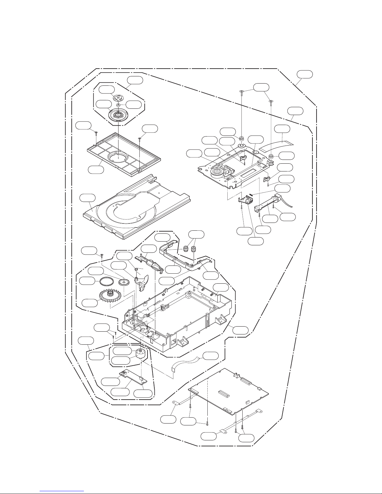
2. DECK MECHANISM SECTION(RL-05S)
1001
A001
A000
A60
1434
1434
1025
1025
1030
1437
1432
1038
1029
1432
1021
1432
1432
1032
1033
1011
1019
1020
1019
1009
1012
1013
1435
1014
1016
1015
1017
1018
1018A
1018B
1018C
1018E
1018D
1006
1436
1024
1433
1029
1027
1027
1005
1026
1003
1002
A004
A002
1041
1042
1434
1434
2-4
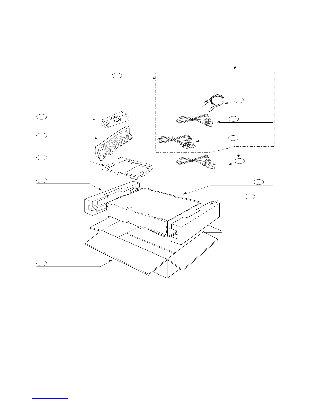
808 Battery
Cable, Coaxial
Plug Ass’y, 1Way
Plug Ass’y, 2Way
Bag
Packing
Remote Control
Instruction Ass’y
Packing
Box
806
804
803
811
812
FLAT CABLE
822
801
900
802
803
810
CABLE ASS’Y
OPTIONAL PART
3. Packing Accessory Section

3-1
SECTION 3
ELECTRICAL
CONTENTS
HDR PART
ELECTRICAL TROUBLESHOOTING GUIDE . . . . . . . . . . . . . . . . . . . . . . . . . . . . . . . . . . . . . . . . . . . . . . . . . . . . . . . .3-2
1. SMPS I/O PART . . . . . . . . . . . . . . . . . . . . . . . . . . . . . . . . . . . . . . . . . . . . . . . . . . . . . . . . . . . . . . . . . . . . . . . . . .3-2
2. SMPS DVD/HDD PART . . . . . . . . . . . . . . . . . . . . . . . . . . . . . . . . . . . . . . . . . . . . . . . . . . . . . . . . . . . . . . . . . . . . .3-5
3. SYSTEM CIRCUIT PART . . . . . . . . . . . . . . . . . . . . . . . . . . . . . . . . . . . . . . . . . . . . . . . . . . . . . . . . . . . . . . . . . . .3-8
4. DISC NOT RECOGNIZED. . . . . . . . . . . . . . . . . . . . . . . . . . . . . . . . . . . . . . . . . . . . . . . . . . . . . . . . . . . . . . . . . . .3-8
5. WHEN PLAYING DISC, NO AUDIO OUTPUT . . . . . . . . . . . . . . . . . . . . . . . . . . . . . . . . . . . . . . . . . . . . . . . . . . . .3-9
6. NO OPTICAL/DIGITAL OUTPUT . . . . . . . . . . . . . . . . . . . . . . . . . . . . . . . . . . . . . . . . . . . . . . . . . . . . . . . . . . . . .3-10
7. NO TUNER AUDIO OUTPUT . . . . . . . . . . . . . . . . . . . . . . . . . . . . . . . . . . . . . . . . . . . . . . . . . . . . . . . . . . . . . . . .3-11
8. NO EXTERNAL INPUT AUDIO . . . . . . . . . . . . . . . . . . . . . . . . . . . . . . . . . . . . . . . . . . . . . . . . . . . . . . . . . . . . . .3-12
9. NO RGB/COMPONENT VIDEO SIGNAL WHEN PLAY DISC . . . . . . . . . . . . . . . . . . . . . . . . . . . . . . . . . . . . . . . .3-13
10. NO COMPOSITE/S-VIDEO SIGNAL WHEN PLAY DISC . . . . . . . . . . . . . . . . . . . . . . . . . . . . . . . . . . . . . . . . . .3-13
11. NO TV, EXTERNAL INPUT VIDEO SIGNAL . . . . . . . . . . . . . . . . . . . . . . . . . . . . . . . . . . . . . . . . . . . . . . . . . . .3-14
12. NO DV(IEEE 1394)INPUT(VIDEO/AUDIO) SIGNAL . . . . . . . . . . . . . . . . . . . . . . . . . . . . . . . . . . . . . . . . . . . . . .3-15
BLOCK DIAGRAMS . . . . . . . . . . . . . . . . . . . . . . . . . . . . . . . . . . . . . . . . . . . . . . . . . . . . . . . . . . . . . . . . . . . . . . . . . .3-16
1. OVERALL BLOCK DIAGRAM . . . . . . . . . . . . . . . . . . . . . . . . . . . . . . . . . . . . . . . . . . . . . . . . . . . . . . . . . . . . . . .3-16
2. LAYOUT CONNECTION BLOCK DIAGRAM_1 . . . . . . . . . . . . . . . . . . . . . . . . . . . . . . . . . . . . . . . . . . . . . . . . . .3-18
3. LAYOUT CONNECTION BLOCK DIAGRAM_2 . . . . . . . . . . . . . . . . . . . . . . . . . . . . . . . . . . . . . . . . . . . . . . . . . .3-20
4. LAYOUT CONNECTION BLOCK DIAGRAM_3 . . . . . . . . . . . . . . . . . . . . . . . . . . . . . . . . . . . . . . . . . . . . . . . . . .3-22
5. SMPS BLOCK DIAGRAM . . . . . . . . . . . . . . . . . . . . . . . . . . . . . . . . . . . . . . . . . . . . . . . . . . . . . . . . . . . . . . . . . .3-24
6. POWER : MAIN BOARD BLOCK DIAGRAM . . . . . . . . . . . . . . . . . . . . . . . . . . . . . . . . . . . . . . . . . . . . . . . . . . . .3-26
7. POWER : I/O BOARD BLOCK DIAGRAM . . . . . . . . . . . . . . . . . . . . . . . . . . . . . . . . . . . . . . . . . . . . . . . . . . . . . .3-28
8. IN/OUT BLOCK DIAGRAM . . . . . . . . . . . . . . . . . . . . . . . . . . . . . . . . . . . . . . . . . . . . . . . . . . . . . . . . . . . . . . . . .3-30
9. VIDEO IN/OUT BLOCK DIAGRAM . . . . . . . . . . . . . . . . . . . . . . . . . . . . . . . . . . . . . . . . . . . . . . . . . . . . . . . . . . .3-32
10. AUDIO BLOCK DIAGRAM . . . . . . . . . . . . . . . . . . . . . . . . . . . . . . . . . . . . . . . . . . . . . . . . . . . . . . . . . . . . . . . . .3-34
11. AUDIO IN/OUT BLOCK DIAGRAM . . . . . . . . . . . . . . . . . . . . . . . . . . . . . . . . . . . . . . . . . . . . . . . . . . . . . . . . . . .3-36
12. FLD / µ-COM / TUNER BLOCK DIAGRAM . . . . . . . . . . . . . . . . . . . . . . . . . . . . . . . . . . . . . . . . . . . . . . . . . . . .3-38
CIRCUIT DIAGRAMS . . . . . . . . . . . . . . . . . . . . . . . . . . . . . . . . . . . . . . . . . . . . . . . . . . . . . . . . . . . . . . . . . . . . . . . . .3-40
1. POWER CIRCUIT DIAGRAM . . . . . . . . . . . . . . . . . . . . . . . . . . . . . . . . . . . . . . . . . . . . . . . . . . . . . . . . . . . . . . . .3-40
2. E5 BGA, POWER, UART2_RS232C CIRCUIT DIAGRAM . . . . . . . . . . . . . . . . . . . . . . . . . . . . . . . . . . . . . . . . . .3-42
3. DDR SDRAM, FLASH, DDR TERMINATION, REG CIRCUIT DIAGRAM . . . . . . . . . . . . . . . . . . . . . . . . . . . . . . .3-44
4. RST, CONTROL/STATUS REG, ADDRESS LATCH CIRCUIT DIAGRAM . . . . . . . . . . . . . . . . . . . . . . . . . . . . . . .3-46
5. 1394, HDMI TRANSMITTER, JACK, ETHERNET CIRCUIT DIAGRAM . . . . . . . . . . . . . . . . . . . . . . . . . . . . . . . . .3-48
6. VIDEO DECODER, IO, JACK CIRCUIT DIAGRAM . . . . . . . . . . . . . . . . . . . . . . . . . . . . . . . . . . . . . . . . . . . . . . .3-50
7. ATAPI 1/2, MEMORY CARD, I/O CIRCUIT DIAGRAM . . . . . . . . . . . . . . . . . . . . . . . . . . . . . . . . . . . . . . . . . . . . .3-52
8. JACK CIRCUIT DIAGRAM . . . . . . . . . . . . . . . . . . . . . . . . . . . . . . . . . . . . . . . . . . . . . . . . . . . . . . . . . . . . . . . . . .3-54
9. I/O µ-COM CIRCUIT DIAGRAM . . . . . . . . . . . . . . . . . . . . . . . . . . . . . . . . . . . . . . . . . . . . . . . . . . . . . . . . . . . . . .3-56
10. TUNER/MPX/ADC/DAC/JACK CIRCUIT DIAGRAM . . . . . . . . . . . . . . . . . . . . . . . . . . . . . . . . . . . . . . . . . . . . . .3-58
11. KEY CIRCUIT DIAGRAM ( 5 TOOL ONLY ) . . . . . . . . . . . . . . . . . . . . . . . . . . . . . . . . . . . . . . . . . . . . . . . . . . . .3-60
12. KEY CIRCUIT DIAGRAM ( 6 TOOL ONLY ) . . . . . . . . . . . . . . . . . . . . . . . . . . . . . . . . . . . . . . . . . . . . . . . . . . . .3-62
13. KEY CIRCUIT DIAGRAM ( 8 TOOL ONLY ) . . . . . . . . . . . . . . . . . . . . . . . . . . . . . . . . . . . . . . . . . . . . . . . . . . . .3-64
14. KEY CIRCUIT DIAGRAM ( 9 TOOL ONLY ) . . . . . . . . . . . . . . . . . . . . . . . . . . . . . . . . . . . . . . . . . . . . . . . . . . . .3-66
15. TIMER CIRCUIT DIAGRAM ( 5 TOOL ONLY ) . . . . . . . . . . . . . . . . . . . . . . . . . . . . . . . . . . . . . . . . . . . . . . . . . .3-68
16. TIMER CIRCUIT DIAGRAM ( 6 TOOL ONLY ) . . . . . . . . . . . . . . . . . . . . . . . . . . . . . . . . . . . . . . . . . . . . . . . . . .3-70
17. TIMER CIRCUIT DIAGRAM ( 8 TOOL ONLY ) . . . . . . . . . . . . . . . . . . . . . . . . . . . . . . . . . . . . . . . . . . . . . . . . . .3-72
18. TIMER CIRCUIT DIAGRAM ( 9 TOOL ONLY ) . . . . . . . . . . . . . . . . . . . . . . . . . . . . . . . . . . . . . . . . . . . . . . . . . .3-74
•
WAVEFORMS . . . . . . . . . . . . . . . . . . . . . . . . . . . . . . . . . . . . . . . . . . . . . . . . . . . . . . . . . . . . . . . . . . . . . . . . . . . . . .3-76
•
CIRCUIT VOLTAGE CHART . . . . . . . . . . . . . . . . . . . . . . . . . . . . . . . . . . . . . . . . . . . . . . . . . . . . . . . . . . . . . . . . . . .3-78
PRINTED CIRCUIT DIAGRAMS . . . . . . . . . . . . . . . . . . . . . . . . . . . . . . . . . . . . . . . . . . . . . . . . . . . . . . . . . . . . . . . . .3-84
1. MAIN P.C.BOARD(TOP SIDE) . . . . . . . . . . . . . . . . . . . . . . . . . . . . . . . . . . . . . . . . . . . . . . . . . . . . . . . . . . . . . .3-84
2. MAIN P.C.BOARD(BOTTOM SIDE) . . . . . . . . . . . . . . . . . . . . . . . . . . . . . . . . . . . . . . . . . . . . . . . . . . . . . . . . . . .3-86
3. I/O P.C.BOARD . . . . . . . . . . . . . . . . . . . . . . . . . . . . . . . . . . . . . . . . . . . . . . . . . . . . . . . . . . . . . . . . . . . . . . . . . .3-88
4. JACK P.C.BOARD . . . . . . . . . . . . . . . . . . . . . . . . . . . . . . . . . . . . . . . . . . . . . . . . . . . . . . . . . . . . . . . . . . . . . . . .3-88
5. HDD P.C.BOARD . . . . . . . . . . . . . . . . . . . . . . . . . . . . . . . . . . . . . . . . . . . . . . . . . . . . . . . . . . . . . . . . . . . . . . . . .3-90
6. POWER P.C.BOARD . . . . . . . . . . . . . . . . . . . . . . . . . . . . . . . . . . . . . . . . . . . . . . . . . . . . . . . . . . . . . . . . . . . . . .3-91
7. KEY P.C.BOARD . . . . . . . . . . . . . . . . . . . . . . . . . . . . . . . . . . . . . . . . . . . . . . . . . . . . . . . . . . . . . . . . . . . . . . . . .3-92
8. TIMER(LED) P.C.BOARD . . . . . . . . . . . . . . . . . . . . . . . . . . . . . . . . . . . . . . . . . . . . . . . . . . . . . . . . . . . . . . . . . .3-93

3-2
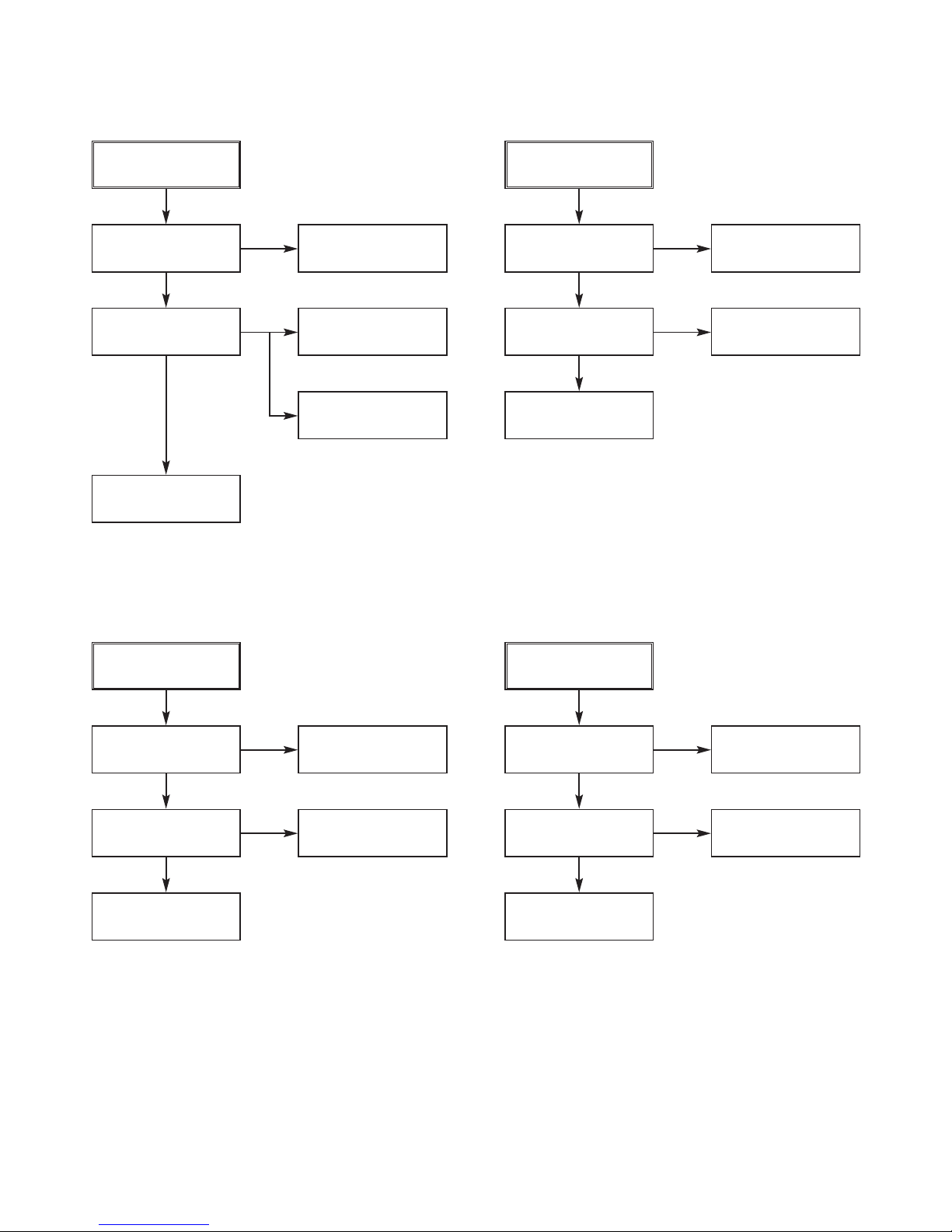
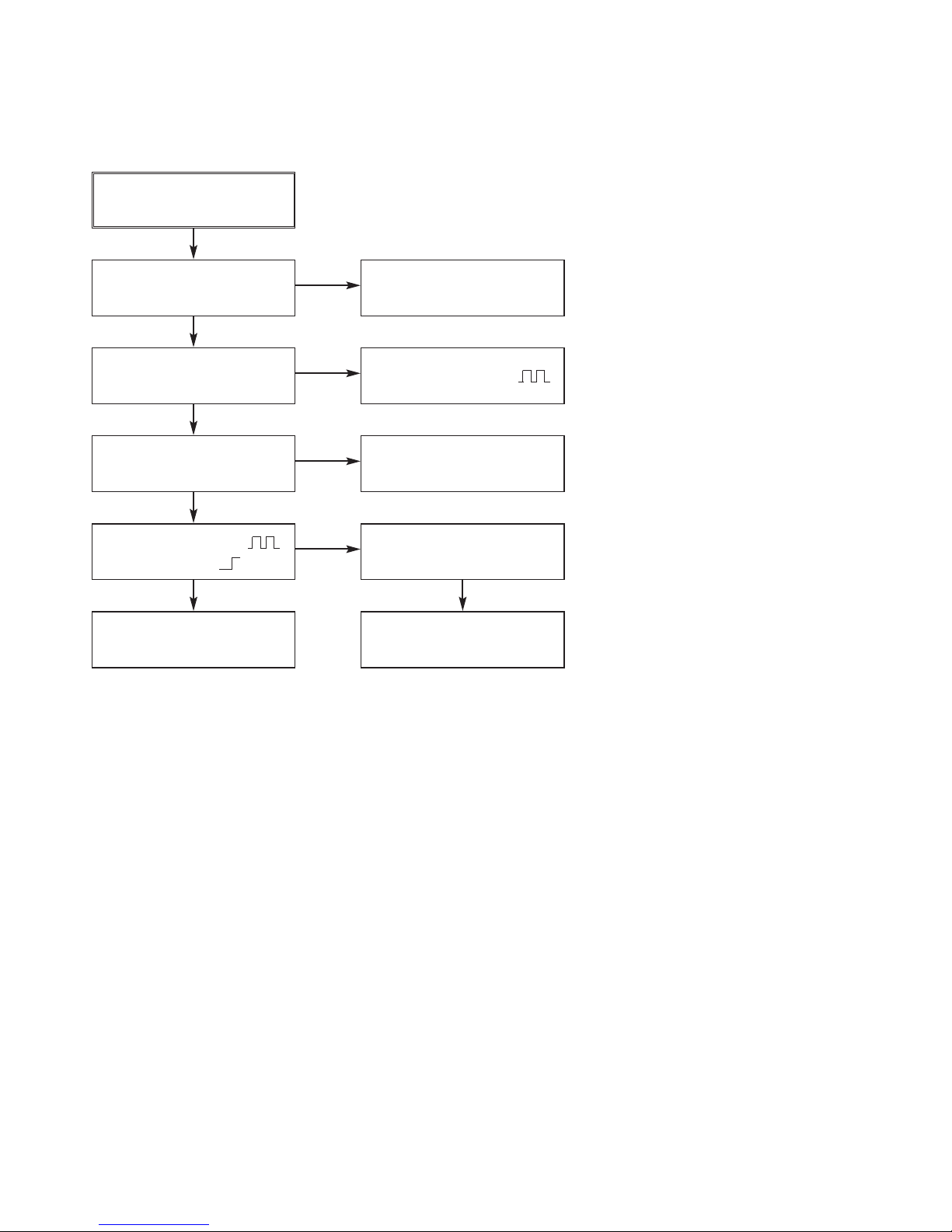
ELECTRICAL TROUBLESHOOTING GUIDE
HDR PART
Replace the BD101
Replace the F101
(Use the same Fuse)
No 5.3VA
Is the F101 Normal?
Is the R101 Normal?
Is the Vcc (10V - 17V)
supplied to IC101 Pin2?
Is the BD101 Normal?
Is the D121 normal?
Is there about 2.5V at the
IC103 Pin1?
Is the D126 normal?
Is the D130 Normal?
Is the D127 Normal?
Is the D128 Normal?
Power Line of I/O PCB
is short
NO
NO
NO
YES
YES
YES
YES
YESYES
YES
YES
YES
YES
YES
YES
Replace the R101
NO
NO
NO
Is the D102 normal?
Check or Replace the
D102
Replace the D121
Replace the IC103
NO
Replace the D126
NO
Replace the D130
NO
Replace the D127
NO
Replace the D128
1. SMPS I/O PART
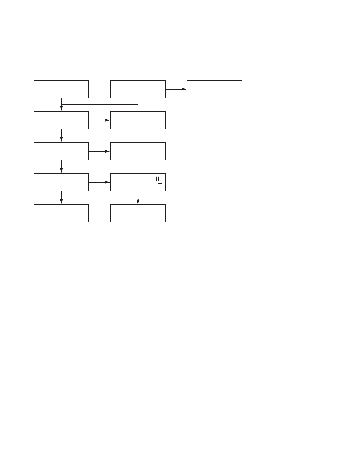
3-3
No 12V
Is there about 3.8V
at the IC153 pin1?
Check or Replace
the D126
Is there about 3.3V~
5V at the IC153 pin4?
Check the ‘PWR CTL
“H”’ signal from µ-com
Check the IC153
and Replace
YES
YES
YES
No 5VT
Check or Replace
the D126
Is the Vcc(14V) supplied to Q124 Emittor?
Check or Replace
the D124
Is the Vcc(33V) supplied to Q124 Base?
NO
NO
Check the ‘TIMER “H”’
signal from µ-com
NO
Check the 33V Line
YES
YES
YES
No 5VD
Check or Replace
the D126
Check the ‘Power CTL
“H”’ signal from µ-com
Is the Vcc(14V) supplied to Q120 Emittor?
Is the Q120 Base
‘H’?
Check or Replace
the Q124
NO
NO
YES
YES
YES
No 12VA /12VT
Check or Replace
the D126
Is there about 14V
at the IC156 pin1?
Is there about 3.3V~
5V at the IC156 pin4?
NO NO
Check the ‘TIMER “H”’
signal from µ-com
NO NO
YES
YES
Check the IC156
and Replace
YES
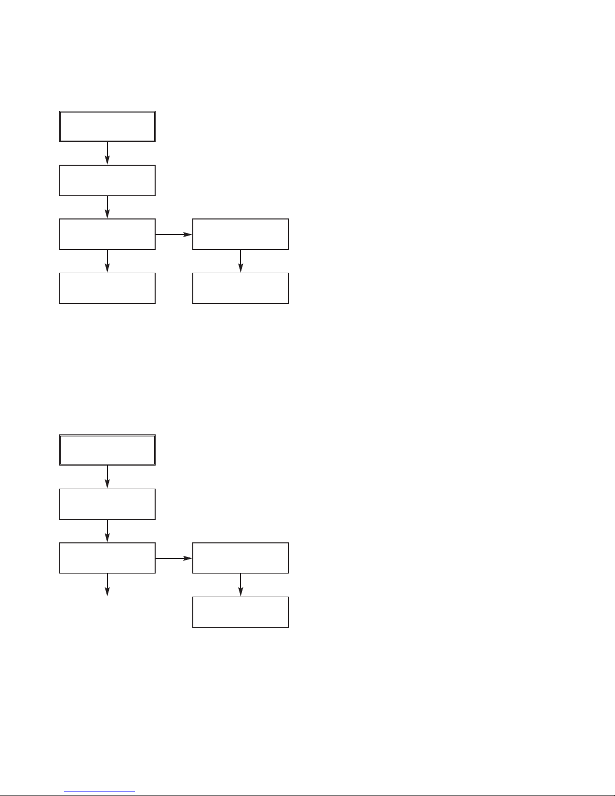
3-4
NO VFD
Check or Replace
the R107
Is the R107
Normal?
Is the D128
Normal?
NO
NO
Check or Replace
the D128
NO
Check or Replace
the ZD151
YES
YES
YES
Is the ZD151
Normal?
Check or Replace
the D127
YES
No 33V
Check or Replace
the D130
Check the ‘PWR CTL
“H”’ signal from µ-com
Is the Vcc(33V) supplied to Q123 Emittor?
Is the Q123 Base
‘H’?
Check or Replace
the Q123
NO
NO
YES
YES
YES
3-5
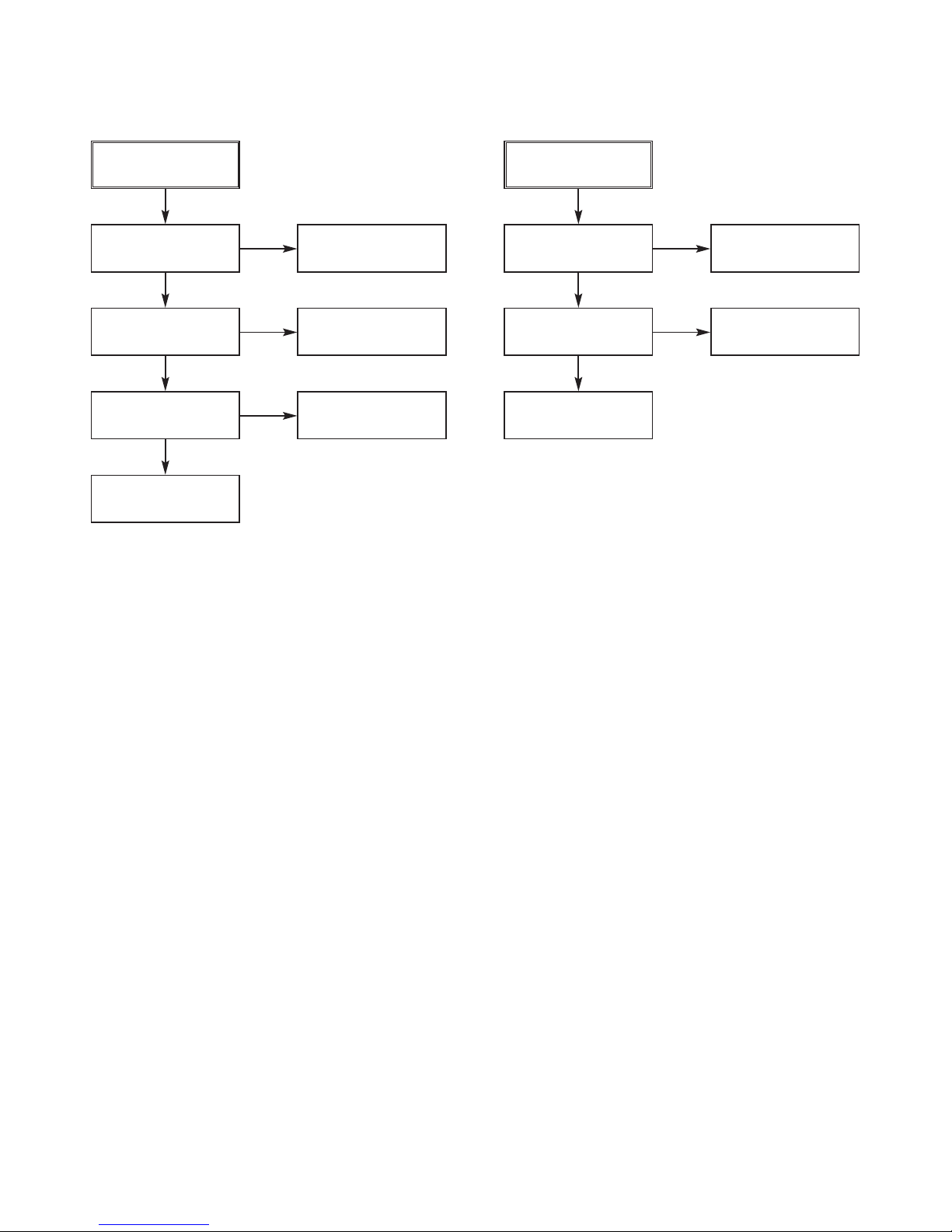
Replace the BD101
Replace the F101
(Use the same Fuse)
No 3.8VA
Is the F101 Normal?
Is the TH01 Normal?
Is Vcc (11V -18V) supplied
to IC101 Pin3?
Is the BD101 Normal?
Are the D122 normal?
Is there about 2.5V at the
IC106 Pin1?
Is the D123 normal?
Is the D124 Normal?
Is the D125 Normal?
Power Line of Main
PCB(VDR) is short
NO
NO
NO
YES
YES
YES
YES
YESYES
YES
YES
YES
YES
YES
Replace the TH01
NO
NO
NO
Is the Q111 normal?
Check or Replace the Q111
Replace the D122
Replace the IC106
NO
Replace the D123
NO
Replace the D124
NO
Replace the D125
2. SMPS DVD/HDD PART
3-6
No 3.3V
Check or Replace
the D122
Check the ‘PWR CTL
“H”’signal from µ-com
Is there about 3.8V at
the IC154 pin1?
Is there about 3.3V~
5V at the IC154 pin4?
Check the IC154
and Replace
NO
NO
YES
YES
YES
No 5.0V
Is there about 5.5V
at the IC151 pin1?
Check or Replace
the D124
Is there about 3.3V~ 5V
at the IC151 pin4?
Check the ‘PWR CTL
“H”’signal from µ-com
Check the IC151
and Replace
YES
YES
YES
NO
NO
No 2.5V
Check or Replace
the D122
Is there about 3.8V
at the IC152 pin1?
Is there about 3.3V~ 5V
at the IC152 pin4?
NO
Check the ‘PWR CTL
“H”’signal from µ-com
NO
YES
YES
Check the IC152
and Replace
YES
No 1.8V
Check or Replace
the D123
Check the ‘PWR CTL
“H”’signal from µ-com
Is there about 2.3V at
the IC160 pin1?
Is there about 3.3V~ 5V
at the IC160 pin4?
Are the R167,R168
normal?
NO
NO
Check or Replace
the R151,R153
NO
YES
YES
YES
Check the IC160
and Replace
YES
3-7
No 12V
Check or Replace
the D125
Check the ‘PWR CTL
“H”’signal from µ-com
Is there about 13.5V
at the IC157 pin1?
Is there about 3.3V~ 5V
at the IC157 pin2?
Check the IC157
and Replace
NO
NO
YES
YES
YES
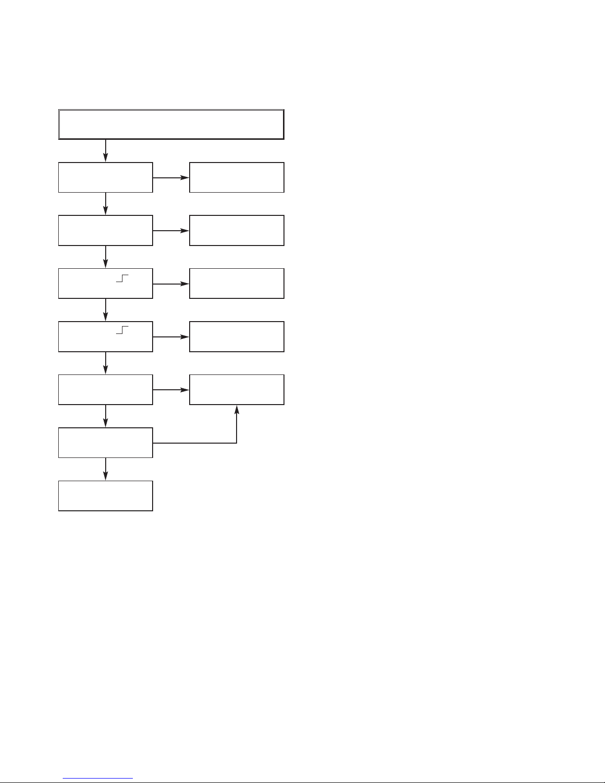
3-8
“Please wait” displayed
Continue at Power On?
Check PN802-22
IC 701-19
IC 307-5: ?
(/HOST-RESET)
X101: Clock oscillated?
(27MHz)
NO
Replace X101
NO
Check IC206 & (Flash
MENORY) IC101
NO
IC 101 DEFECT
NO
YES
YES
R146 : ?
IC 206-26 : ?
YES
R180, R181 : ?
YES
3. SYSTEM Circuit PART
Check DRIVER Power?
5V. 12V
Change MEDIA TEST
Check J601
Check SMPS
NO
NO
YES
4. DISC not recognized
CHECK
IC808- pin2, 4 (VCC) :
pin32,33(SLC/CLK) :
IC 805-pin14,19(z_mute_R/L):
IC701-pin58(A_mute_L) :
CHECK
IC 805-pin1,2,3,4 :
Pin10(reset) :
Pin7,8(I2C) :
3-9
5. When playing DISC, no Audio output
CHECK IC802-pin3, 6,
13(VCC)
Replace IC802
YES
YES
IC805-pin15,18
(Audio_out R/L) : Is
there a signal?
CHECK Q801, 802,
803, 804, 806
C841, C842 on I/O
PCB Is there a signal?
Only “Without SCART model”
IC 808-pin21, 22, 25,
26:Is there a signal?
YES
YES
NO
IC101
DEFECT
NO
NO
C8A3, C8A4 on I/O
PCB Is there a signal?
YES
NO
YES
L821,L836: Is there
a signal?
YES
CHECK Cable connections & TV Audio mute.
YES
3-10
R101:
CHECK PN802-pin2
(SPDIF_OUT) :
R933 :
CHECK JK803 & RCA
cable connection
NO
YES
YES
YES
CHECK JK805 & Optic
cable connection
IC101 DEFECT
NO
6. No OPTICAL/DIGITAL Output
3-11
7. No TUNER Audio Output
TU801-pin16(SIF):
Is there a signal?
IC812-30,31:
Is there a signal?
IC809-pin7, IC810-pin7: Is
there a signal?
Check C920
Is there a signal?
Check R839,R841:
YES
YES
IC802-pin10,12:
Is there a signal?
YES
IC802-pin2,4,7,8 :
Pin9(reset) :
When playing DISC, no
Audio output
YES
YES YES
NO
NO
CHECK
IC811 : Power & In/Out PIN
NO
CHECK
IC802-pin3,6,13(VCC)
NO
Replace IC802
3-12
8. No External input Audio
CHECK Cable connections & Input signal.
Check R839,R841:
?
IC809-pin7, IC810-pin7:
Is there a signal?
IC809,IC810-pin3:
Is there a signal?
IC809,IC810-pin1:
Is there a signal?
< AV1 > < AV2 >
IC802-pin10,12:
Is there a signal?
NO
NO
CHECK IC811 :
Power & In/Out PIN
IC802-pin2,4,7,8 :
Pin9(reset) :
When playing DISC,
no Audio output
NO
NO
NO
YES
NO
IC802-pin2,4,7,8 :
Pin9(reset) :
NO
When playing DISC,
no Audio output
YES
3-13
9. No RGB/Component Video signal when play DISC
R131,R132,R133:
Is there a signal?
PN801-7,8,9:
Is there a signal?
IC807-pin24,21,18
Is there a signal?
CHECK SW801 statue &
SW801-in2(RGB_SEL”H”)
NO
CHECK IC807pin1,16(+5.2V)
Replace IC807
YES
YES
YES
YES
10. No composite/s-video Signal when play DISC
R128,R129,R130:
Is there a signal?
PN801-2,4,6:
Is there a signal?
IC807-27,30,32:
Is there a signal?
NO
CHECK IC807pin1,16(+5.2V)
Replace IC807
YES
YES
YES
YES
3-14
11. No TV, External input Video signal
CHECK Signal path
on the I/O board
C540 : Is there a
signal?
Check PN802-pin22
IC 701: reset circuit
Replace IC501
YES
YES
C532,C535,C537:
Is there a signal?
C538:Is there a
signal?
No video signal of external
input AV3 (Rear RCA input)
No video signal of external
input AV4 (composite,s-video)
When Cable connecting Tuner and Rear
SCART1,2 No TV video signal(AV1/2)
NO NO NO
NO
NO
YES
YES
NO
YES
YES
YES
NO
CHECK Cable connections & Input signal.
IC501- pin34
(reset”H”) :
IC501- pin40 (VI_CLK) : X501
clock oscillated? (14.318MHz)
YES
CHECK No RGB/ component/composite Signal when play DISC
YES
3-15
12. No DV(IEEE 1394)input(Video/Audio) signal
Check DV_Jack and CABLE(CN501)
connection
DV-mode
switching ?
IC401 power 3.3V
IC 401-37: “High”
&X401 oscillated?(24.576MHz)
NO
CHECK SMPS
+3.3V
NO
Change to DV-mode.
Using Remote Control
NO
NO
NO
YES
CHECK Reset
Circuit
YES
YES
YES
IC401-15
Is there a signal?
YES
IC401-pin1, 27, 28, 29,
30: Is there a signal?
YES
IC401-pin 2, 3 :
Is there a signal?
YES
IC101 DEFECT
YES
Check DV Cable
Replace IC401
3-16 3-17
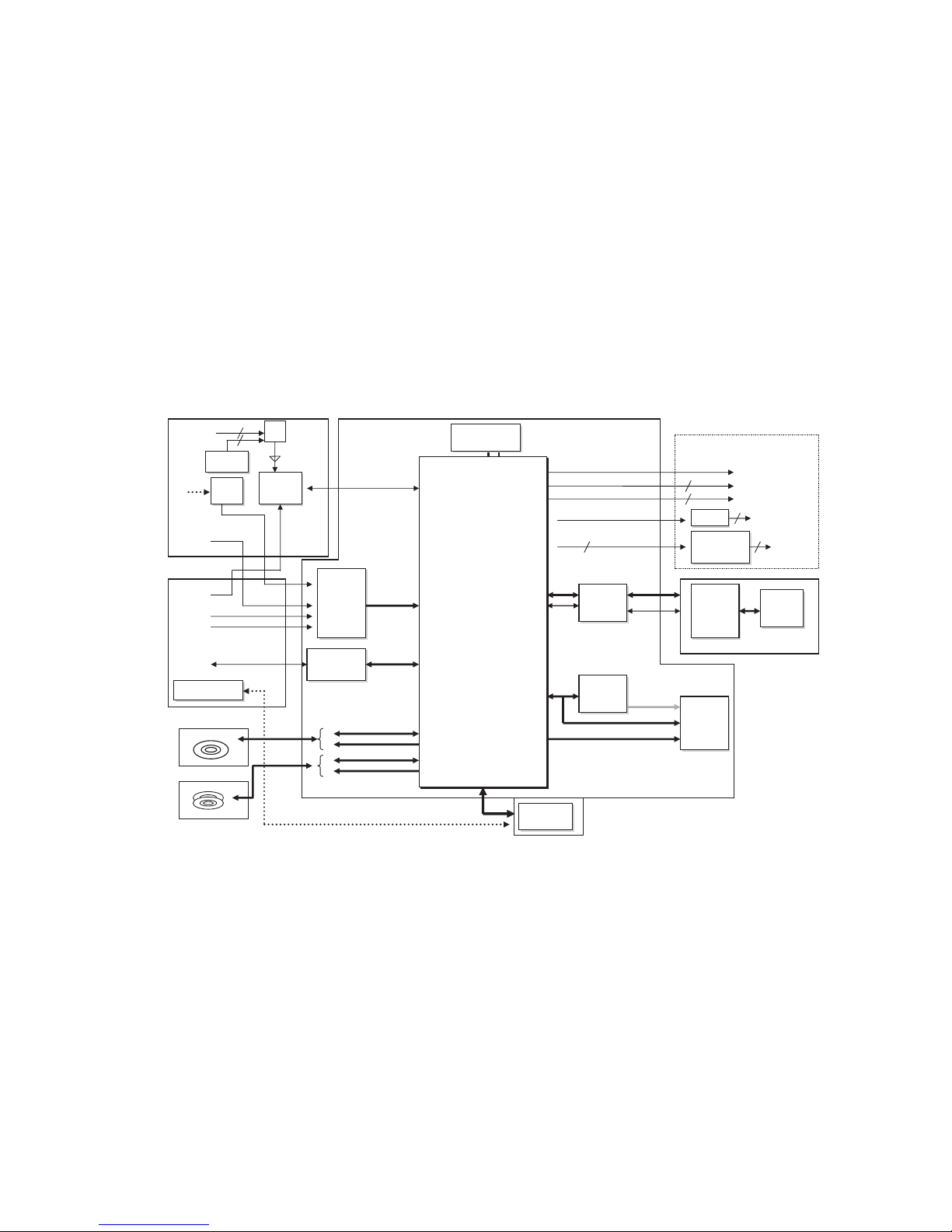
BLOCK DIAGRAMS
1. Overall Block Diagram
Front Driv er IC
Front Driv er IC
V_DEC
Decoder
TVP5146
V_DEC
Decoder
TVP5146
A_ADC
CS5340
A_ADC
CS5340
RF
A1_In
Tuner
Tuner
S/PDIF
S/PDIF
DMN8652
DMN8652
SW
A_ADC: 2ch
CS4351
A_ADC: 2ch
CS4351
V2_In
S_In
A2_In
I/O B'd
Front Timer& J ac k
B'd
AI_D0
V1_I
N
CVBS_Out
I/O B'd
S_VIDEO_Out
Y/Pb/P
r
Anal og
Audio Out
Opti cal & Di gital
Audio Out
BIO_PHY_DATA[0:7]
PHY
TSB41LV03A
PHY
TSB41LV03A
DV_In
HD[0:15]
HD[0:15]
SPI I/O Interface
ATA_CONTROL
A0_D
0
A0_IEC958
VOUT_CVB
S
ATAPI1_DATA[0:15]
ATAPI1 _...
DVD DRIVER
DDR SDRAM
32M WordX2
DDR SDRAM
32M WordX2
32M WordX2
I/O B'd
U-COM
U-COM
SIO_SPI_CS#0
SIO_SPI_MISO
SIO_SPI_MOSI
MAIN B'd
Latch
74LVT16373
Latch
74LVT16373
HA[6:21]
Flash
8MByte
Flash
8MByte
V1_In
N/A2
MSP3425
N/A2
MSP3425
HA[1:5],HA22
PHY
SAIN
ASTEL
PHY
SAIN
ASTEL
Buffer
74VC245
74LVC541
Buffer
74VC245
74LVC
541
SOCKET
x2
SOCKET
x2
HDD
ATAPI2_DATA[0:15]
ATAPI2 _...
VOUT_Y_C
VOUT_Y/Pb/Pr_R/G/B
3-18 3-19
2. Layout Connection Block Diagram_1
SMPS
Board
ATAPI 1
Jack
Board
DVD + RW DRIVER
5VA5V5VT
3.3V
12VA
12V
33VT
Input/Output Boa rd
Front Board
Key
Board
S1/S2 AV3/S/Comp/DigitalOptical
12V
5V
AV3,DV_in
S/Jack
-24V
VF+
VF-
Tuner
HARD DISC DRIVER
ATAPI 2
J601
HDMI
AV4/S/DV
1.8V
2.5V
5VT
3.3V
12V
5V
CN101
CN502
J603
PN7101
PN7102
PN7901
PN7902
PN801
P1701
PN802
CN601
CN501
J602
P1T01
P1M01
P1D01
Main Board
J1
P9701 P9702
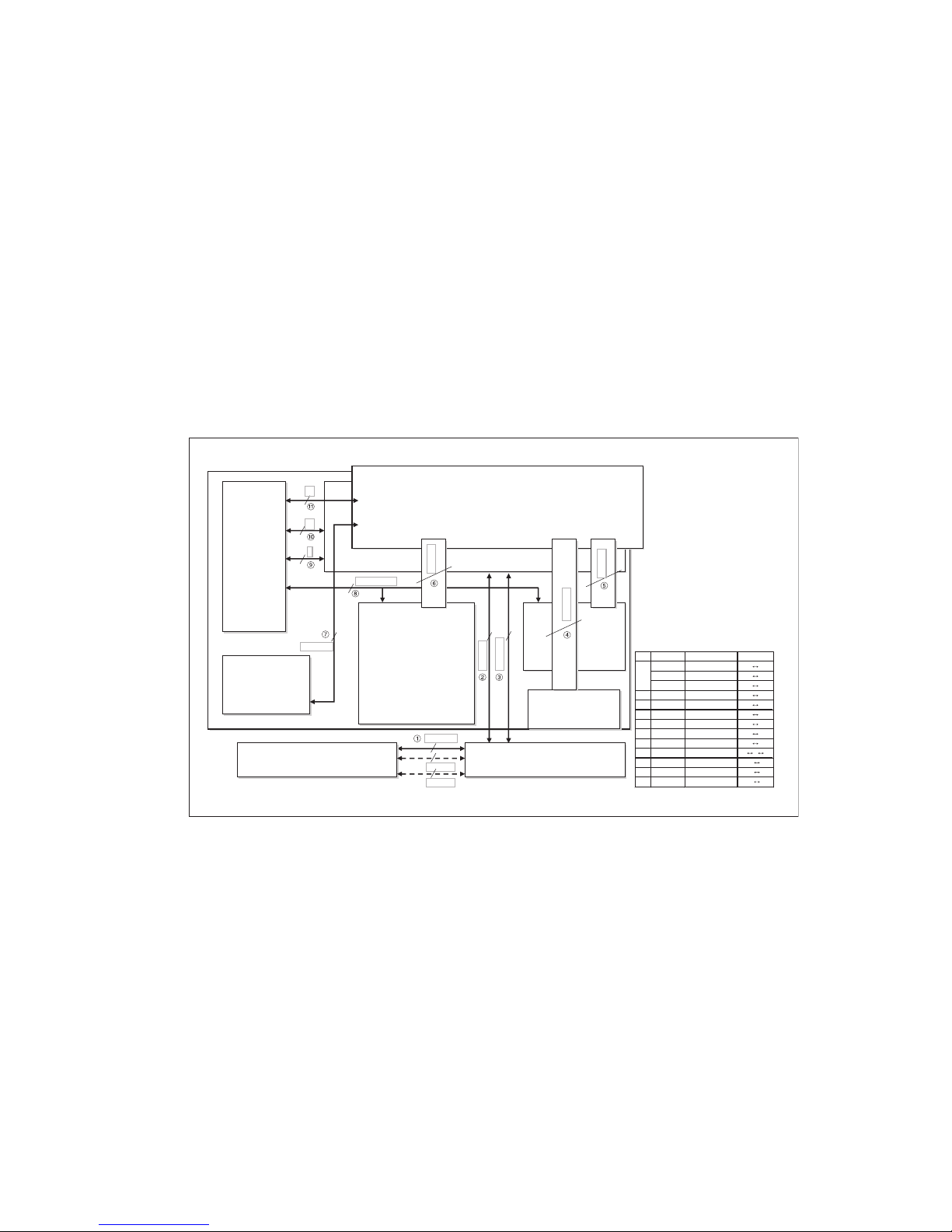
3-20 3-21
3. Layout Connection Block Diagram_2
Timer(FLD)
Load er
Load er
9-in-2 Memory
(3-in-1 Mem ory)
9-in-2 Memory
(3-in-1 Mem ory)
SMPS
SMPS
Jack
Jack
Main Bdí
Main Bd'
Timer 1(K ey)
In / Out Bd'
HDD
10:160mm
6:280mm
12:290mm
7:160mm
40:250mm
40:80mm
40:80mm
15:220mm
4:160/320mm
5
15
13
Pin No. P/N
10P(8T) 6631R-E09
2E
7P1 (5.9T) 6631R-E092F
3P(6T) 6631R-E092G
6P 6631R-E066F
12P 6631R-E066E
40P
40P 6850R-EA08Y
40P 6850R-EA08Y
15P 6631R-E044D
4P/6P 6631R-H003A P L H
5P 6631R-E092D P I
15P 6631R-E092C P I
13P 6631R-E025S P I
3:160mm
K
K
K
M
M
m
H
L
J
T
T
T
T
T
M
M
M
M
2
3
4
5
6
7
8
9
10
11
 Loading...