

LG 60GA6400-UD Schematic
Internal Use Only
North/Latin America http://aic.lgservice.com
Europe/Africa http://eic.lgservice.com
Asia/Oceania http://biz.lgservice.com
LED TV
SERVICE MANUAL
CHASSIS : LA37G
MODEL : 60GA6400 60GA6400-UD
CAUTION
BEFORE SERVICING THE CHASSIS,
READ THE SAFETY PRECAUTIONS IN THIS MANUAL.
Printed in KoreaP/NO : MFL67657908 (1306-REV01)

CONTENTS
CONTENTS .............................................................................................. 2
PRODUCT SAFETY ................................................................................. 3
SERVICING PRECAUTIONS .................................................................... 4
SPECIFICATION ....................................................................................... 6
ADJUSTMENT INSTRUCTION .............................................................. 11
EXPLODED VIEW .................................................................................. 20
SCHEMATIC CIRCUIT DIAGRAM ..............................................................
Only for training and service purposes
- 2 -
LGE Internal Use OnlyCopyright © LG Electronics. Inc. All rights reserved.
SAFETY PRECAUTIONS
IMPORTANT SAFETY NOTICE
Many electrical and mechanical parts in this chassis have special safety-related characteristics. These parts are identified by in the
Schematic Diagram and Exploded View.
It is essential that these special safety parts should be replaced with the same components as recommended in this manual to prevent
Shock, Fire, or other Hazards.
Do not modify the original design without permission of manufacturer.
General Guidance
An isolation Transformer should always be used during the
servicing of a receiver whose chassis is not isolated from the AC
power line. Use a transformer of adequate power rating as this
protects the technician from accidents resulting in personal injury
from electrical shocks.
It will also protect the receiver and it's components from being
damaged by accidental shorts of th e cir cuitry that may be
inadvertently introduced during the service operation.
If any fuse (or Fusible Resistor) in this TV receiver is blown,
replace it with the specified.
When replacing a high wattage resistor (Oxide Metal Film Resistor,
over 1 W), keep the resistor 10 mm away from PCB.
Keep wires away from high voltage or high temperature parts.
Before returning the receiver to the customer,
always perform an AC leakage current check on the exposed
metallic parts of the cabinet, such as antennas, terminals, etc., to
be sure the set is safe to operate without damage of electrical
shock.
Leakage Current Cold Check(Antenna Cold Check)
With the instrument AC plug removed from AC source, connect an
electrical jumper across the two AC plug prongs. Place the AC
switch in the on position, connect one lead of ohm-meter to the AC
plug prongs tied together and touch other ohm-meter lead in turn to
each exposed metallic parts such as antenna terminals, phone
jacks, etc.
If the exposed metallic part has a return path to the chassis, the
measured resistance should be between 1 MΩ and 5.2 MΩ.
When the exposed metal has no return path to the chassis the
reading must be infinite.
An other abnormality exists that must be corrected before the
receiver is returned to the customer.
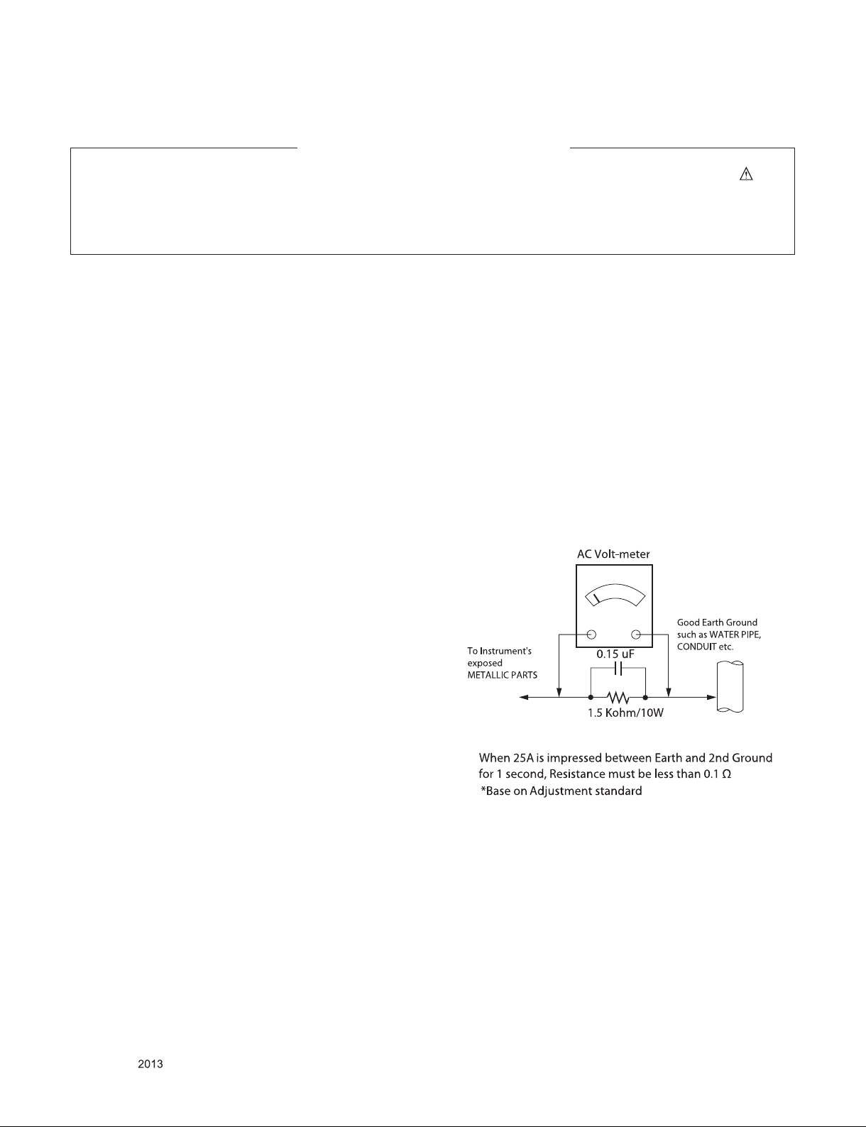
Leakage Current Hot Check (See below Figure)
Plug the AC cord directly into the AC outlet.
Do not use a line Isolation Transformer during this check.
Connect 1.5 K / 10 watt resistor in parallel with a 0.15 uF capacitor
between a known good earth ground (Water Pipe, Conduit, etc.)
and the exposed metallic parts.
Measure the AC voltage across the resistor using AC voltmeter
with 1000 ohms/volt or more sensitivity.
Reverse plug the AC cord into the AC outlet and repeat AC voltage
measurements for each exp ose d metallic par t. Any voltage
measured must not exceed 0.75 volt RMS which is corresponds to
0.5 mA.
In case any measurement is out of the limits specified, there is
possibility of shock hazard and the set must be checked and
repaired before it is returned to the customer.
Leakage Current Hot Check circuit
Only for training and service purposes
- 3 -
LGE Internal Use OnlyCopyright © LG Electronics. Inc. All rights reserved.

SERVICING PRECAUTIONS
CAUTION: Before servicing receivers covered by this service
manual and its supplements and addenda, read and follow the
SAFETY PRECAUTIONS on page 3 of this publication.
NOTE: If unforeseen circumstances create conict between the
following servicing precautions and any of the safety precautions
on page 3 of this publication, always follow the safety precautions.
Remember: Safety First.
General Servicing Precautions
1. Always unplug the receiver AC power cord from the AC power
source before;
a. Removing or reinstalling any component, circuit board mod-
ule or any other receiver assembly.
b. Disconnecting or reconnecting any receiver electrical plug or
other electrical connection.
c. Connecting a test substitute in parallel with an electrolytic
capacitor in the receiver.
CAUTION: A wrong part substitution or incorrect polarity
installation of electrolytic capacitors may result in an explosion hazard.
2. Test high voltage only by measuring it with an appropriate
high voltage meter or other voltage measuring device (DVM,
FETVOM, etc) equipped with a suitable high voltage probe.
Do not test high voltage by "drawing an arc".
3. Do not spray chemicals on or near this receiver or any of its
assemblies.
4. Unless specied otherwise in this service manual, clean
electrical contacts only by applying the following mixture to the
contacts with a pipe cleaner, cotton-tipped stick or comparable
non-abrasive applicator; 10 % (by volume) Acetone and 90 %
(by volume) isopropyl alcohol (90 % - 99 % strength)
CAUTION: This is a ammable mixture.
Unless specied otherwise in this service manual, lubrication of
contacts in not required.
5. Do not defeat any plug/socket B+ voltage interlocks with which
receivers covered by this service manual might be equipped.
6. Do not apply AC power to this instrument and/or any of its
electrical assemblies unless all solid-state device heat sinks are
correctly installed.
7. Always connect the test receiver ground lead to the receiver
chassis ground before connecting the test receiver positive
lead.
Always remove the test receiver ground lead last.
8. Use with this receiver only the test xtures specied in this
service manual.
CAUTION: Do not connect the test xture ground strap to any
heat sink in this receiver.
Electrostatically Sensitive (ES) Devices
Some semiconductor (solid-state) devices can be damaged easily by static electricity. Such components commonly are called
Electrostatically Sensitive (ES) Devices. Examples of typical ES
devices are integrated circuits and some eld-effect transistors
and semiconductor “chip” components. The following techniques
should be used to help reduce the incidence of component damage caused by static by static electricity.
1. Immediately before handling any semiconductor component or
semiconductor-equipped assembly, drain off any electrostatic
charge on your body by touching a known earth ground. Alternatively, obtain and wear a commercially available discharging
wrist strap device, which should be removed to prevent potential shock reasons prior to applying power to the unit under test.
2. After removing an electrical assembly equipped with ES
devices, place the assembly on a conductive surface such as
aluminum foil, to prevent electrostatic charge buildup or exposure of the assembly.
3. Use only a grounded-tip soldering iron to solder or unsolder ES
devices.
4. Use only an anti-static type solder removal device. Some solder
removal devices not classied as “anti-static” can generate
electrical charges sufcient to damage ES devices.
5. Do not use freon-propelled chemicals. These can generate
electrical charges sufcient to damage ES devices.
6. Do not remove a replacement ES device from its protective
package until immediately before you are ready to install it.
(Most replacement ES devices are packaged with leads electrically shorted together by conductive foam, aluminum foil or
comparable conductive material).
7. Immediately before removing the protective material from the
leads of a replacement ES device, touch the protective material
to the chassis or circuit assembly into which the device will be
installed.
CAUTION: Be sure no power is applied to the chassis or circuit,
and observe all other safety precautions.
8. Minimize bodily motions when handling unpackaged replacement ES devices. (Otherwise harmless motion such as the
brushing together of your clothes fabric or the lifting of your
foot from a carpeted oor can generate static electricity sufcient to damage an ES device.)
General Soldering Guidelines
1. Use a grounded-tip, low-wattage soldering iron and appropriate
tip size and shape that will maintain tip temperature within the
range or 500 °F to 600 °F.
2. Use an appropriate gauge of RMA resin-core solder composed
of 60 parts tin/40 parts lead.
3. Keep the soldering iron tip clean and well tinned.
4. Thoroughly clean the surfaces to be soldered. Use a mall wirebristle (0.5 inch, or 1.25 cm) brush with a metal handle.
Do not use freon-propelled spray-on cleaners.
5. Use the following unsoldering technique
a. Allow the soldering iron tip to reach normal temperature.
(500 °F to 600 °F)
b. Heat the component lead until the solder melts.
c. Quickly draw the melted solder with an anti-static, suction-
type solder removal device or with solder braid.
CAUTION: Work quickly to avoid overheating the circuit
board printed foil.
6. Use the following soldering technique.
a. Allow the soldering iron tip to reach a normal temperature
(500 °F to 600 °F)
b. First, hold the soldering iron tip and solder the strand against
the component lead until the solder melts.
c. Quickly move the soldering iron tip to the junction of the
component lead and the printed circuit foil, and hold it there
only until the solder ows onto and around both the component lead and the foil.
CAUTION: Work quickly to avoid overheating the circuit
board printed foil.
d. Closely inspect the solder area and remove any excess or
splashed solder with a small wire-bristle brush.
Only for training and service purposes
- 4 -
LGE Internal Use OnlyCopyright © LG Electronics. Inc. All rights reserved.

IC Remove/Replacement
Some chassis circuit boards have slotted holes (oblong) through
which the IC leads are inserted and then bent at against the circuit foil. When holes are the slotted type, the following technique
should be used to remove and replace the IC. When working with
boards using the familiar round hole, use the standard technique
as outlined in paragraphs 5 and 6 above.
Removal
1. Desolder and straighten each IC lead in one operation by
gently prying up on the lead with the soldering iron tip as the
solder melts.
2. Draw away the melted solder with an anti-static suction-type
solder removal device (or with solder braid) before removing
the IC.
Replacement
1. Carefully insert the replacement IC in the circuit board.
2. Carefully bend each IC lead against the circuit foil pad and
solder it.
3. Clean the soldered areas with a small wire-bristle brush.
(It is not necessary to reapply acrylic coating to the areas).
"Small-Signal" Discrete Transistor
Removal/Replacement
1. Remove the defective transistor by clipping its leads as close
as possible to the component body.
2. Bend into a "U" shape the end of each of three leads remaining
on the circuit board.
3. Bend into a "U" shape the replacement transistor leads.
4. Connect the replacement transistor leads to the corresponding
leads extending from the circuit board and crimp the "U" with
long nose pliers to insure metal to metal contact then solder
each connection.
Power Output, Transistor Device
Removal/Replacement
1. Heat and remove all solder from around the transistor leads.
2. Remove the heat sink mounting screw (if so equipped).
3. Carefully remove the transistor from the heat sink of the circuit
board.
4. Insert new transistor in the circuit board.
5. Solder each transistor lead, and clip off excess lead.
6. Replace heat sink.
Diode Removal/Replacement
1. Remove defective diode by clipping its leads as close as possible to diode body.
2. Bend the two remaining leads perpendicular y to the circuit
board.
3. Observing diode polarity, wrap each lead of the new diode
around the corresponding lead on the circuit board.
4. Securely crimp each connection and solder it.
5. Inspect (on the circuit board copper side) the solder joints of
the two "original" leads. If they are not shiny, reheat them and if
necessary, apply additional solder.
3. Solder the connections.
CAUTION: Maintain original spacing between the replaced
component and adjacent components and the circuit board to
prevent excessive component temperatures.
Circuit Board Foil Repair
Excessive heat applied to the copper foil of any printed circuit
board will weaken the adhesive that bonds the foil to the circuit
board causing the foil to separate from or "lift-off" the board. The
following guidelines and procedures should be followed whenever
this condition is encountered.
At IC Connections
To repair a defective copper pattern at IC connections use the
following procedure to install a jumper wire on the copper pattern
side of the circuit board. (Use this technique only on IC connections).
1. Carefully remove the damaged copper pattern with a sharp
knife. (Remove only as much copper as absolutely necessary).
2. carefully scratch away the solder resist and acrylic coating (if
used) from the end of the remaining copper pattern.
3. Bend a small "U" in one end of a small gauge jumper wire and
carefully crimp it around the IC pin. Solder the IC connection.
4. Route the jumper wire along the path of the out-away copper
pattern and let it overlap the previously scraped end of the
good copper pattern. Solder the overlapped area and clip off
any excess jumper wire.
At Other Connections
Use the following technique to repair the defective copper pattern
at connections other than IC Pins. This technique involves the
installation of a jumper wire on the component side of the circuit
board.
1. Remove the defective copper pattern with a sharp knife.
Remove at least 1/4 inch of copper, to ensure that a hazardous
condition will not exist if the jumper wire opens.
2. Trace along the copper pattern from both sides of the pattern
break and locate the nearest component that is directly connected to the affected copper pattern.
3. Connect insulated 20-gauge jumper wire from the lead of the
nearest component on one side of the pattern break to the lead
of the nearest component on the other side.
Carefully crimp and solder the connections.
CAUTION: Be sure the insulated jumper wire is dressed so the
it does not touch components or sharp edges.
Fuse and Conventional Resistor
Removal/Replacement
1. Clip each fuse or resistor lead at top of the circuit board hollow
stake.
2. Securely crimp the leads of replacement component around
notch at stake top.
Only for training and service purposes
- 5 -
LGE Internal Use OnlyCopyright © LG Electronics. Inc. All rights reserved.
SPECIFICATION
NOTE : Specifications and others are subject to change without notice for improvement
.
1. Application range
This spec sheet is applied LED TV with (LA37G) chassis
2. Test condition
Each part is tested as below without special notice.
1)
Temperature : 25
2) Relative Humidity: 65 % ± 10 %
3) Power Voltage
- AC 100-240 V~, 50/60 Hz
* Standard Voltage of each products is marked by models.
4) Specification and performance of each parts are followed
ea ch drawing and s pe cificatio n b y p art number in
accordance with BOM.
5) The receiver must be operated for about 5 minutes prior to
the adjustment.
ºC
± 5 ºC (77±9 ºF), CST : 40±5
ºC
3. Test method
1) Performance: LGE TV test method followed
2) Demanded other specification
- Safety : UL, CSA, CE, IEC specification
- EMC: FCC, ICES, CE, IEC specification
- Wireless : Wireless HD Specification (Option)
4. General Specification
No Item Specication Remark
1 Market 1) North America
2 Television System NTSC-M, ATSC, 64 & 256 QAM
3 Program Coverage VHF 2-13, UHF 14-69, CATV 1-135
DTV 2-69, CADTV 1-135
4 Input Voltage AC 100 ~ 240V 50/60Hz
5 Available Channel 1) VHF : 02~13
2) UHF : 14~69
3) DTV : 02-69
4) CATV : 01~135
5) CADTV : 01~135
6 Screen Size 42 inch Wide(1920 × 1080)
47 inch Wide(1920 × 1080)
50 inch Wide(1920 × 1080)
55 inch Wide(1920 × 1080)
60 inch Wide(1920 × 1080)
7 Aspect Ratio 16:9
8 Tuning System FS
9 LCD Module LC420EUN-SFF2 Edge T120Hz
LC470EUN-SFF2 Edge T120Hz
LC500EUN-SFF1 Edge T120Hz
LC550EUN-SFF2 Edge T120Hz
LC470EUH-LFF1 Ad.CINEMA T240Hz
LC550EUH-LFF1 Ad.CINEMA T240Hz
JE600D3LC87 Edge M120Hz
10 Operating Environment 1) Temp : 0 ~ 40 deg
2) Humidity : ~ 80 %
11 Storage Environment 1) Temp : -20 ~ 60 deg
2) Humidity : ~ 85 %
Only for training and service purposes
- 6 -
LGE Internal Use OnlyCopyright © LG Electronics. Inc. All rights reserved.
5. External input format
5.1. 2D mode
5.1.1. Component input (Y, CB/PB, CR/PR)
No. Resolution H-freq(kHz) V-freq.(kHz) Pixel clock Proposed
1. 720*480 15.73 60.00 13.5135 SDTV ,DVD 480I
2. 720*480 15.73 59.94 13.50 SDTV ,DVD 480I
3. 720*480 31.50 60.00 27.027 SDTV 480P
4. 720*480 31.47 59.94 27.00 SDTV 480P
5. 1280*720 45.00 60.00 74.25 HDTV 720P
6. 1280*720 44.96 59.94 74.176 HDTV 720P
7. 1920*1080 33.75 60.00 74.25 HDTV 1080I
8. 1920*1080 33.72 59.94 74.176 HDTV 1080I
9. 1920*1080 67.50 60.00 148.50 HDTV 1080P
10. 1920*1080 67.432 59.94 148.352 HDTV 1080P
11. 1920*1080 27.00 24.00 74.25 HDTV 1080P
12. 1920*1080 26.97 23.94 74.176 HDTV 1080P
13. 1920*1080 33.75 30.00 74.25 HDTV 1080P
14. 1920*1080 33.71 29.97 74.176 HDTV 1080P
5.1.2. HDMI Input 1 (PC/DTV)
No Resolution H-freq(kHz) V-freq.(Hz) Pixel clock(MHz) Proposed
HDMI-PC
1 640*350 31.468 70.09 25.17 EGA Х
2 720*400 31.469 70.08 28.32 DOS O
3 640*480 31.469 59.94 25.17 VESA(VGA) O
4 800*600 37.879 60.31 40.00 VESA(SVGA) O
5 1024*768 48.363 60.00 65.00 VESA(XGA) O
6 1360*768 47.712 60.015 85.50 VESA (WXGA) O
7 1280*1024 63.981 60.020 108.00 VESA (SXGA) O
8 1920*1080 67.5 60 148.5 HDTV 1080P O
HDMI-DTV
1 720*480 31.50 60.00 27.027 SDTV 480P
2 720*480 31.47 59.94 27.00 SDTV 480P
3 1280*720 45.00 60.00 74.25 HDTV 720P
4 1280*720 44.96 59.94 74.176 HDTV 720P
5 1920*1080 33.75 60.00 74.25 HDTV 1080I
6 1920*1080 33.72 59.94 74.176 HDTV 1080I
7 1920*1080 67.50 60.00 148.50 HDTV 1080P
8 1920*1080 67.432 59.94 148.352 HDTV 1080P
9 1920*1080 27.00 24.00 74.25 HDTV 1080P
10 1920*1080 26.97 23.976 74.176 HDTV 1080P
11 1920*1080 33.75 30.00 74.25 HDTV 1080P
12 1920*1080 33.71 29.97 74.176 HDTV 1080P
Only for training and service purposes
- 7 -
LGE Internal Use OnlyCopyright © LG Electronics. Inc. All rights reserved.
5.2. 3D mode
5.2.1. RF Input
No Resolution H-freq(kHz) V-freq.(Hz) Pixel clock(MHz) Proposed Remark
1 1920*1080 45 60 74.25 HDTV 1080I Side by Side, Top & Bottom
2 1280*720 45 60 74.25 HDTV 720P Side by Side, Top & Bottom
5.2.2. HDMI-PC Input Input
No Resolution H-freq(kHz) V-freq.(Hz) Pixel clock(MHz) Remark
1 1024*768 48.363 60.004 65.000 Side by Side , Top & Bottom
2 1280*768 47.776 59.870 79.500 Side by Side , Top & Bottom
3 1360*768 47.712 60.015 85.500 Side by Side , Top & Bottom
4 1280*720 45.00 60.00 74.25 Side by Side , Top & Bottom,
Single Frame Sequential
5 1920*1080 67.50 60.00 148.50 Side by Side , Top & Bottom
Checkerboard, Single Frame Sequential
Row Interleaving, Column Interleaving
5.2.3. HDMI 1.3(3D supported mode manually)
No Resolution H-freq(kHz) V-freq.(Hz) Pixel clock(MHz) Remark
1 1280*720p 45.00 60.00 74.25 Side by Side , Top & Bottom,
Single Frame Sequential
2 1920*1080i 33.75 60.00 74.25 Side by Side , Top & Bottom
3 1920*1080p 67.50 60.00 148.50 Side by Side , Top & Bottom
Checkerboard, Single Frame Sequential
Row Interleaving, Column Interleaving
4 1920*1080p 27.00 24.000 74.25 Side by Side , Top & Bottom
Checkerboard
5 1920*1080p 33.75 30.000 74.25 Side by Side, Top & Bottom
Checkerboard
Only for training and service purposes
- 8 -
LGE Internal Use OnlyCopyright © LG Electronics. Inc. All rights reserved.
5.2.4. HDMI 1.4a(3D supported mode automatically)
No Resolution H-freq(kHz) V-freq.(Hz) Pixel clock(MHz) Proposed Remark
1 1280*720p 89.91 / 90.00 59.94 / 60.00 148.35 / 148.50 Mandatory Frame Packing,
2 1280*720p 44.96 / 45.00 59.94 / 60.00 74.18 / 74.25 Mandatory Top & Bottom
3 1920*1080i 33.72 / 33.75 59.94 / 60.00 74.18 / 74.25 Mandatory Side by Side (Half)
4 1920*1080p 43.94 / 54.00 23.97 / 24.00 148.35 / 148.50 Mandatory Frame Packing,
5 1920*1080p 26.97 / 27.00 23.97 / 24.00 74.18 / 74.25 Mandatory Top & Bottom
6 1280*720p 44.96 / 45.00 59.94 / 60.00 74.18 / 74.25 Primary Side by Side (Half)
7 1920*1080i 67.432 / 67.50 59.94 / 60.00 148.35 / 148.50 Primary Frame Packing
8 1920*1080p 67.43 / 67.50 59.94 / 60.00 148.35 / 148.50 Primary Top & Bottom
9 1920*1080p 26.97 / 27.00 23.97 / 24.00 74.18 / 74.25 Primary Side by Side (Half)
10 1920*1080p 67.432 / 67.50 29.976 / 30.00 148.35 / 148.50 Primary Frame Packing,
11 1920*1080p 33.716 / 33.75 29.976 / 30.00 74.18 / 74.25 Primary Top & Bottom
12 1920*1080i 33.72 / 33.75 59.94 / 60.00 74.18 / 74.25 Secondary Top & Bottom
13 1920*1080p 67.43 / 67.50 59.94 / 60.00 148.35 / 148.50 Secondary Side by Side (Half)
14 1920*1080p 33.716 / 33.75 29.976 / 30.00 74.18 / 74.25 Secondary Side by Side (Half)
15 720*480p 62.938 / 63.00 59.94 / 60.00 54.00 / 54.054 Secondary (16:9) Frame Packing,
16 720*480p 31.469 / 31.50 59.94 / 60.00 27.00 / 27.027 Secondary (16:9) Top & Bottom
17 720*480p 31.469 / 31.50 59.94 / 60.00 27.00 / 27.027 Secondary (16:9) Side by Side (Half)
18 720*480p 62.938 / 63.00 59.94 / 60.00 54.00 / 54.054 Secondary (4:3) Frame Packing,
19 720*480p 31.469 / 31.50 59.94 / 60.00 27.00 / 27.027 Secondary (4:3) Top & Bottom
20 720*480p 31.469 / 31.50 59.94 / 60.00 27.00 / 27.027 Secondary (4:3) Side by Side (Half)
21 640*480p 62.938 / 63.00 59.94 / 60.00 50.35 / 50.40 Secondary Frame Packing,
22 640*480p 31.469 / 31.50 59.94 / 60.00 25.175 / 25.20 Secondary Top & Bottom
23 640*480p 31.469 / 31.50 59.94 / 60.00 25.175 / 25.20 Secondary Side by Side (Half)
24 1280*720p 89.91 / 90.00 59.94 / 60.00 148.35 / 148.50 Line Alternative
25 1280*720p 44.96 / 45.00 59.94 / 60.00 148.35 / 148.50 Side by Side (Full)
26 1920*1080i 67.432 / 67.50 59.94 / 60.00 148.35 / 148.50 Field Alternative
27 1920*1080i 33.72 / 33.75 59.94 / 60.00 148.35 / 148.50 Side by Side (Full)
28 1920*1080p 43.94 / 54.00 23.97 / 24.000 148.35 / 148.50 Line Alternative
29 1920*1080p 26.97 / 27.00 23.97 / 24.000 148.35 / 148.50 Side by Side (Full)
30 1920*1080p 67.432 / 67.50 29.976 / 30.00 148.35 / 148.50 Line Alternative
31 1920*1080p 33.716 / 33.75 29.976 / 30.00 148.35 / 148.50 Side by Side (Full)
32 720*480p 62.938 / 63.00 59.94 / 60.00 54.00 / 54.054 16:9 Line Alternative
33 720*480p 31.469 / 31.50 59.94 / 60.00 54.00 / 54.054 16:9 Side by Side (Full)
34 720*480p 62.938 / 63.00 59.94 / 60.00 54.00 / 54.054 4:3 Line Alternative
35 720*480p 31.469 / 31.50 59.94 / 60.00 54.00 / 54.054 4:3 Side by Side (Full)
36 640*480p 62.938 / 63.00 59.94 / 60.00 50.35 / 50.40 Line Alternative
37 640*480p 31.469 / 31.50 59.94 / 60.00 50.35 / 50.40 Side by Side (Full)
Only for training and service purposes
- 9 -
LGE Internal Use OnlyCopyright © LG Electronics. Inc. All rights reserved.
R
L
R
L
5.2.5. USB Input
No Resolution H-freq(kHz) V-freq.(Hz) Pixel clock(MHz) Proposed Remark
1 1920*1080 33.75 30.000 74.25 HDTV 1080p Side by Side
Top & Bottom
Checkerboard
5.2.6. Component Input
No Resolution H-freq(kHz) V-freq.(Hz) Pixel clock(MHz) Proposed Remark
1 1280*720 44.96 59.94 74.176 HDTV 720P Side by Side, Top & Bottom
2 1920*1080 33.75 60.00 74.25 HDTV 1080I Side by Side, Top & Bottom
3 1920*1080 33.72 59.94 74.176 HDTV 1080I Side by Side, Top & Bottom
4 1920*1080 67.500 60 148.50 HDTV 1080P Side by Side, Top & Bottom
5 1920*1080 67.432 59.94 148.352 HDTV 1080P Side by Side, Top & Bottom
6 1920*1080 27.000 24.000 74.25 HDTV 1080P Side by Side, Top & Bottom
7 1920*1080 26.97 23.976 74.176 HDTV 1080P Side by Side, Top & Bottom
8 1920*1080 33.75 30.000 74.25 HDTV 1080P Side by Side, Top & Bottom
9 1920*1080 33.71 29.97 74.176 HDTV 1080P Side by Side, Top & Bottom
5.3. 2D to 3D Mode
- Remark: 3D Input mode
No. Side by Side Top & Bottom Checkerboard Single Frame
Sequential
1
Frame Packing Line
Interleaving
Column
Interleaving
Only for training and service purposes
- 10 -
LGE Internal Use OnlyCopyright © LG Electronics. Inc. All rights reserved.

ADJUSTMENT INSTRUCTION
1. Application Range
This spec. sheet applies to L9(LG1152) Chassis applied LED
TV all models manufactured in TV factory
2. Specification
(1) Because this is not a hot chassis, it is not necessary to use
an isolation transformer. However, the use of isolation
transformer will help protect test instrument.
(2) Adjustment must be done in the correct order.
(3) The adjustment must be performed in the circumstance of
25 ±5 °C of temperature and 65±10% of relative humidity if
there is no specific designation.
(4) The input voltage of the receiver must keep 100~240V,
50/60Hz.
(5) The receiver must be operated for about 5 minutes prior to
the adjustment when module is in the circumstance of over
15 °C
In case of keeping module is in the circumstance of 0°C, it
should be placed in the circumstance of above 15°C for 2
hours
In case of keeping module is in the circumstance of below
-20°C, it should be placed in the circumstance of above
15°C for 3 hours.
[Caution]
When still image is displayed for a period of 20 minutes or
longer (especially where W/B scale is strong.
Digital pattern 13ch and/or Cross hatch pattern 09ch), there
can some afterimage in the black level area
3.3. Automatic Adjustment
3.3.1. Overview
ADC adjustment is needed to find the optimum black level and
gain in Analog-to-Digital device and to compensate RGB
deviation
3.3.2. Equipment & Condition
1) Jig (RS-232C protocol)
2) Inner Pattern
- Resolution : 1080p (Inner Pattern)
- Resolution : 1024*768 RGB (Inner Pattern)
- Pattern : Horizontal 100% Color Bar Pattern
- Pattern level : 0.7±0.1 Vp-p
3.3.3 Adjustment
3.3.3.1. Adjustment method
▪ Using RS-232, adjust items listed in 3.1 in the other shown in
“4.1.3.3”
3.3.3.2. Adj. protocol
Protocol Command Set ACK
Enter adj. mode aa 00 00 a 00 OK00x
Source change xb 00 40
xb 00 60
Begin adj. ad 00 10
Return adj. result OKx (Case of Success)
Read adj. data (main)
ad 00 20
b 00 OK40x (Adjust 480i Comp1 )
b 00 OK60x (Adjust 1024*768 RGB)
NGx (Case of Fail)
(main)
000000000000000000000000007c007b006dx
3. Adjustment items
3.1. Final assembly adjustment
▪ EDID/DDC check
▪ White Balance adjustment
▪ ADC Adjustment check
▪ RS-232C functionality check
▪ Factory Option setting per destination
▪ Ship-out mode setting (In-Stop)
3.2. Etc
▪ Ship-out mode
▪ Tool option menu
▪ USB Download(S/W Update, Option, Service only)
(sub )
ad 00 21
Conrm adj. ad 00 99 NG 03 00x (Fail)
End adj. aa 00 90 a 00 OK90x
3.3.3.3 Adj. order
▪ aa 00 00 [Enter ADC adj. mode]
▪ xb 00 40 [Change input source to Component1(480i)]
▪ ad 00 10 [Adjust 480i Comp1]
▪ xb 00 60 [Change input source to RGB(1024*768)]
▪ ad 00 10 [Adjust 1024*768 RGB]
▪ ad 00 90 End adj.
Ref) ADC adj. RS232C Protocol_Ver1.0
(Sub)
000000070000000000000000007c00830077x
NG 03 01x (Fail)
NG 03 02x (Fail)
OK 03 03x (Success)
Only for training and service purposes
- 11 -
LGE Internal Use OnlyCopyright © LG Electronics. Inc. All rights reserved.
4. Manual Adjustment
4.1. MAC Address, ESN Key and Widevine
Key download
4.1.1. Equipment & Condition
1) Play file: keydownload.exe
4.1.2. Communication Port connection
1) Key Write: Com 1,2,3,4 and 115200 (Baudrate)
2) Barcode: Com 1,2,3,4 and 9600 (Baudrate)
4.1.3. Download process
1) Select the download items.
2) Mode check: Online Only
3) Check the test process
- U S, Canad a m ode ls : DET EC T -> M AC _WR IT E ->
WIDEVINE_WRITE
- Korea, Me xico models: DE TECT -> MA C_WRITE ->
WIDEVINE_WRITE
4) Play : START
5) Check of result: Ready, Test, OK or NG
6) Printer out (MAC Address Label)
4.1.4. Communication Port connection
1) Connect: PCBA Jig -> RS-232C Port == PC -> RS-232C
Port
4.2. PING Test
* LAN card can be verified by using PING test
4.2.1 Adjustment Method(Board)
(1) Connect LAN to the board and power on.
(Default IP can be set to automatic setting. When power
ON, IP can be automatically be achieved from the router)
(2) Press ADJ key in the adjustment remote control.
(3) Check Network status by pressing 13. ACAP PING TEST in
EZ ADJUST. If it operates properly, it will show “Network is
operating properly.” If it does not, it will show “Network is
not working properly.”
4.2.2 Adjustment Method(Manufacturer)
(4) Connect the PC with PING Test program installed and the
LAN port of the SET via Cross LAN Cable. (The IP setting
of the PC has to be 12.12.2.3)
(5) After the PING Test program has been executed, check the
program setting. (IP of the set will be 12.12.2.2. Double
check the setting. Do not check the Modem because it will
not be used.)
(6) Press the Power Only Key in Adjustment remote control.
(IP of the set will be set)
(7) Upon pressing “RUN” in the program, it will show “OK” or
“NG” according to the test result.
● After all the adjustments, to disable the IP setting, press
INSTOP key.
4.1.5. Download
1) US, Canada models (12Y LCD TV + MAC + Widevine +
ESN + Google CA Key)
4.1.6. Inspection
- In INSTART menu, check these keys.
Only for training and service purposes
- 12 -
LGE Internal Use OnlyCopyright © LG Electronics. Inc. All rights reserved.

4.3 EDID Download
4.3.1 Overview
▪ It is a VESA regulation. A PC or a MNT will display an optimal
resolution through information sharing without any necessity
of user input. It is a realization of “Plug and Play”.
4.3.2 Equipment
▪ Since embedded EDID data is used, EDID download JIG,
HDMI cable and D-sub cable are not need.
▪ Adjust remocon
4.3.3 Download method
1) Press Adj. key on the Adj. R/C,
2) Select EDID D/L menu.
3) By pressing Enter key, EDID download will begin
4) If Download is successful, OK is display, but If Download is
failure, NG is displayed.
5) If Download is failure, Re-try downloads.
※ Caution) When EDID Download, must remove RGB/HDMI
Cable.
4.3.3.1. EDID DATA
4.3.3.1.1. PCM EDID Data
# HDMI 1(C/S : 42 2C)
EDID Block 0, Bytes 0-127 [00H-7FH]
0 1 2 3 4 5 6 7 8 9 A B C D E F
---------------------------------------------------------------------------------------- 0 | 00 FF FF FF FF FF FF 00 1E 6D 01 00 01 01 01 01
10 | 01 17 01 03 80 A0 5A 78 0A EE 91 A3 54 4C 99 26
20 | 0F 50 54 A1 08 00 31 40 45 40 61 40 71 40 81 80
30 | 01 01 01 01 01 01 02 3A 80 18 71 38 2D 40 58 2C
40 | 45 00 A0 5A 00 00 00 1E 66 21 50 B0 51 00 1B 30
50 | 40 70 36 00 A0 5A 00 00 00 1E 00 00 00 FD 00 3A
60 | 3E 1E 53 10 00 0A 20 20 20 20 20 20 00 00 00 FC
70 | 00 4C 47 20 54 56 0A 20 20 20 20 20 20 20 01 42
0 1 2 3 4 5 6 7 8 9 A B C D E F
---------------------------------------------------------------------------------------- 0 | 02 03 2E F1 48 90 22 20 05 04 03 02 01 23 09 57
10 | 07 78 03 0C 00 10 00 B8 2D 20 C0 0E 01 4F 00 FE
20 | 08 10 06 10 18 10 28 10 38 10 E3 05 03 01 02 3A
30 | 80 18 71 38 2D 40 58 2C 45 00 A0 5A 00 00 00 1E
40 | 01 1D 80 18 71 1C 16 20 58 2C 25 00 A0 5A 00 00
50 | 00 9E 01 1D 00 72 51 D0 1E 20 6E 28 55 00 A0 5A
60 | 00 00 00 1E 26 36 80 A0 70 38 1F 40 30 20 25 00
70 | A0 5A 00 00 00 1A 00 00 00 00 00 00 00 00 00 2C
# HDMI 2(C/S : 42 1C)
EDID Block 0, Bytes 0-127 [00H-7FH]
0 1 2 3 4 5 6 7 8 9 A B C D E F
---------------------------------------------------------------------------------------- 0 | 00 FF FF FF FF FF FF 00 1E 6D 01 00 01 01 01 01
10 | 01 17 01 03 80 A0 5A 78 0A EE 91 A3 54 4C 99 26
20 | 0F 50 54 A1 08 00 31 40 45 40 61 40 71 40 81 80
30 | 01 01 01 01 01 01 02 3A 80 18 71 38 2D 40 58 2C
40 | 45 00 A0 5A 00 00 00 1E 66 21 50 B0 51 00 1B 30
50 | 40 70 36 00 A0 5A 00 00 00 1E 00 00 00 FD 00 3A
60 | 3E 1E 53 10 00 0A 20 20 20 20 20 20 00 00 00 FC
70 | 00 4C 47 20 54 56 0A 20 20 20 20 20 20 20 01 42
0 1 2 3 4 5 6 7 8 9 A B C D E F
---------------------------------------------------------------------------------------- 0 | 02 03 2E F1 48 90 22 20 05 04 03 02 01 23 09 57
10 | 07 78 03 0C 00 20 00 B8 2D 20 C0 0E 01 4F 00 FE
20 | 08 10 06 10 18 10 28 10 38 10 E3 05 03 01 02 3A
30 | 80 18 71 38 2D 40 58 2C 45 00 A0 5A 00 00 00 1E
40 | 01 1D 80 18 71 1C 16 20 58 2C 25 00 A0 5A 00 00
50 | 00 9E 01 1D 00 72 51 D0 1E 20 6E 28 55 00 A0 5A
60 | 00 00 00 1E 26 36 80 A0 70 38 1F 40 30 20 25 00
70 | A0 5A 00 00 00 1A 00 00 00 00 00 00 00 00 00 1C
# HDMI 3(C/S : 42 0C)
EDID Block 0, Bytes 0-127 [00H-7FH]
0 1 2 3 4 5 6 7 8 9 A B C D E F
---------------------------------------------------------------------------------------- 0 | 00 FF FF FF FF FF FF 00 1E 6D 01 00 01 01 01 01
10 | 01 17 01 03 80 A0 5A 78 0A EE 91 A3 54 4C 99 26
20 | 0F 50 54 A1 08 00 31 40 45 40 61 40 71 40 81 80
30 | 01 01 01 01 01 01 02 3A 80 18 71 38 2D 40 58 2C
40 | 45 00 A0 5A 00 00 00 1E 66 21 50 B0 51 00 1B 30
50 | 40 70 36 00 A0 5A 00 00 00 1E 00 00 00 FD 00 3A
60 | 3E 1E 53 10 00 0A 20 20 20 20 20 20 00 00 00 FC
70 | 00 4C 47 20 54 56 0A 20 20 20 20 20 20 20 01 42
0 1 2 3 4 5 6 7 8 9 A B C D E F
---------------------------------------------------------------------------------------- 0 | 02 03 2E F1 48 90 22 20 05 04 03 02 01 23 09 57
10 | 07 78 03 0C 00 30 00 B8 2D 20 C0 0E 01 4F 00 FE
20 | 08 10 06 10 18 10 28 10 38 10 E3 05 03 01 02 3A
30 | 80 18 71 38 2D 40 58 2C 45 00 A0 5A 00 00 00 1E
40 | 01 1D 80 18 71 1C 16 20 58 2C 25 00 A0 5A 00 00
50 | 00 9E 01 1D 00 72 51 D0 1E 20 6E 28 55 00 A0 5A
60 | 00 00 00 1E 26 36 80 A0 70 38 1F 40 30 20 25 00
70 | A0 5A 00 00 00 1A 00 00 00 00 00 00 00 00 00 0C
# HDMI 4(C/S : 42 FC)
EDID Block 0, Bytes 0-127 [00H-7FH]
0 1 2 3 4 5 6 7 8 9 A B C D E F
---------------------------------------------------------------------------------------- 0 | 00 FF FF FF FF FF FF 00 1E 6D 01 00 01 01 01 01
10 | 01 17 01 03 80 A0 5A 78 0A EE 91 A3 54 4C 99 26
20 | 0F 50 54 A1 08 00 31 40 45 40 61 40 71 40 81 80
30 | 01 01 01 01 01 01 02 3A 80 18 71 38 2D 40 58 2C
40 | 45 00 A0 5A 00 00 00 1E 66 21 50 B0 51 00 1B 30
50 | 40 70 36 00 A0 5A 00 00 00 1E 00 00 00 FD 00 3A
60 | 3E 1E 53 10 00 0A 20 20 20 20 20 20 00 00 00 FC
70 | 00 4C 47 20 54 56 0A 20 20 20 20 20 20 20 01 42
0 1 2 3 4 5 6 7 8 9 A B C D E F
---------------------------------------------------------------------------------------- 0 | 02 03 2E F1 48 90 22 20 05 04 03 02 01 23 09 57
10 | 07 78 03 0C 00 40 00 B8 2D 20 C0 0E 01 4F 00 FE
20 | 08 10 06 10 18 10 28 10 38 10 E3 05 03 01 02 3A
30 | 80 18 71 38 2D 40 58 2C 45 00 A0 5A 00 00 00 1E
40 | 01 1D 80 18 71 1C 16 20 58 2C 25 00 A0 5A 00 00
50 | 00 9E 01 1D 00 72 51 D0 1E 20 6E 28 55 00 A0 5A
60 | 00 00 00 1E 26 36 80 A0 70 38 1F 40 30 20 25 00
70 | A0 5A 00 00 00 1A 00 00 00 00 00 00 00 00 00 FC
Only for training and service purposes
- 13 -
LGE Internal Use OnlyCopyright © LG Electronics. Inc. All rights reserved.

4.3.3.1.2. AC3 EDID Data
# HDMI 1(C/S : 42 BA)
EDID Block 0, Bytes 0-127 [00H-7FH]
0 1 2 3 4 5 6 7 8 9 A B C D E F
---------------------------------------------------------------------------------------- 0 | 00 FF FF FF FF FF FF 00 1E 6D 01 00 01 01 01 01
10 | 01 17 01 03 80 A0 5A 78 0A EE 91 A3 54 4C 99 26
20 | 0F 50 54 A1 08 00 31 40 45 40 61 40 71 40 81 80
30 | 01 01 01 01 01 01 02 3A 80 18 71 38 2D 40 58 2C
40 | 45 00 A0 5A 00 00 00 1E 66 21 50 B0 51 00 1B 30
50 | 40 70 36 00 A0 5A 00 00 00 1E 00 00 00 FD 00 3A
60 | 3E 1E 53 10 00 0A 20 20 20 20 20 20 00 00 00 FC
70 | 00 4C 47 20 54 56 0A 20 20 20 20 20 20 20 01 42
0 1 2 3 4 5 6 7 8 9 A B C D E F
---------------------------------------------------------------------------------------- 0 | 02 03 31 F1 48 90 22 20 05 04 03 02 01 26 15 07
10 | 50 09 57 07 78 03 0C 00 10 00 B8 2D 20 C0 0E 01
20 | 4F 00 FE 08 10 06 10 18 10 28 10 38 10 E3 05 03
30 | 01 02 3A 80 18 71 38 2D 40 58 2C 45 00 A0 5A 00
40 | 00 00 1E 01 1D 80 18 71 1C 16 20 58 2C 25 00 A0
50 | 5A 00 00 00 9E 01 1D 00 72 51 D0 1E 20 6E 28 55
60 | 00 A0 5A 00 00 00 1E 26 36 80 A0 70 38 1F 40 30
70 | 20 25 00 A0 5A 00 00 00 1A 00 00 00 00 00 00 BA
# HDMI 2(C/S : 42 AA)
EDID Block 0, Bytes 0-127 [00H-7FH]
0 1 2 3 4 5 6 7 8 9 A B C D E F
---------------------------------------------------------------------------------------- 0 | 00 FF FF FF FF FF FF 00 1E 6D 01 00 01 01 01 01
10 | 01 17 01 03 80 A0 5A 78 0A EE 91 A3 54 4C 99 26
20 | 0F 50 54 A1 08 00 31 40 45 40 61 40 71 40 81 80
30 | 01 01 01 01 01 01 02 3A 80 18 71 38 2D 40 58 2C
40 | 45 00 A0 5A 00 00 00 1E 66 21 50 B0 51 00 1B 30
50 | 40 70 36 00 A0 5A 00 00 00 1E 00 00 00 FD 00 3A
60 | 3E 1E 53 10 00 0A 20 20 20 20 20 20 00 00 00 FC
70 | 00 4C 47 20 54 56 0A 20 20 20 20 20 20 20 01 42
0 1 2 3 4 5 6 7 8 9 A B C D E F
---------------------------------------------------------------------------------------- 0 | 02 03 31 F1 48 90 22 20 05 04 03 02 01 26 15 07
10 | 50 09 57 07 78 03 0C 00 20 00 B8 2D 20 C0 0E 01
20 | 4F 00 FE 08 10 06 10 18 10 28 10 38 10 E3 05 03
30 | 01 02 3A 80 18 71 38 2D 40 58 2C 45 00 A0 5A 00
40 | 00 00 1E 01 1D 80 18 71 1C 16 20 58 2C 25 00 A0
50 | 5A 00 00 00 9E 01 1D 00 72 51 D0 1E 20 6E 28 55
60 | 00 A0 5A 00 00 00 1E 26 36 80 A0 70 38 1F 40 30
70 | 20 25 00 A0 5A 00 00 00 1A 00 00 00 00 00 00 AA
# HDMI 3(C/S : 42 9A)
EDID Block 0, Bytes 0-127 [00H-7FH]
0 1 2 3 4 5 6 7 8 9 A B C D E F
---------------------------------------------------------------------------------------- 0 | 00 FF FF FF FF FF FF 00 1E 6D 01 00 01 01 01 01
10 | 01 17 01 03 80 A0 5A 78 0A EE 91 A3 54 4C 99 26
20 | 0F 50 54 A1 08 00 31 40 45 40 61 40 71 40 81 80
30 | 01 01 01 01 01 01 02 3A 80 18 71 38 2D 40 58 2C
40 | 45 00 A0 5A 00 00 00 1E 66 21 50 B0 51 00 1B 30
50 | 40 70 36 00 A0 5A 00 00 00 1E 00 00 00 FD 00 3A
60 | 3E 1E 53 10 00 0A 20 20 20 20 20 20 00 00 00 FC
70 | 00 4C 47 20 54 56 0A 20 20 20 20 20 20 20 01 42
0 1 2 3 4 5 6 7 8 9 A B C D E F
---------------------------------------------------------------------------------------- 0 | 02 03 31 F1 48 90 22 20 05 04 03 02 01 26 15 07
10 | 50 09 57 07 78 03 0C 00 30 00 B8 2D 20 C0 0E 01
20 | 4F 00 FE 08 10 06 10 18 10 28 10 38 10 E3 05 03
30 | 01 02 3A 80 18 71 38 2D 40 58 2C 45 00 A0 5A 00
40 | 00 00 1E 01 1D 80 18 71 1C 16 20 58 2C 25 00 A0
50 | 5A 00 00 00 9E 01 1D 00 72 51 D0 1E 20 6E 28 55
60 | 00 A0 5A 00 00 00 1E 26 36 80 A0 70 38 1F 40 30
70 | 20 25 00 A0 5A 00 00 00 1A 00 00 00 00 00 00 9A
# HDMI 4(C/S : 42 8A)
EDID Block 0, Bytes 0-127 [00H-7FH]
0 1 2 3 4 5 6 7 8 9 A B C D E F
---------------------------------------------------------------------------------------- 0 | 00 FF FF FF FF FF FF 00 1E 6D 01 00 01 01 01 01
10 | 01 17 01 03 80 A0 5A 78 0A EE 91 A3 54 4C 99 26
20 | 0F 50 54 A1 08 00 31 40 45 40 61 40 71 40 81 80
30 | 01 01 01 01 01 01 02 3A 80 18 71 38 2D 40 58 2C
40 | 45 00 A0 5A 00 00 00 1E 66 21 50 B0 51 00 1B 30
50 | 40 70 36 00 A0 5A 00 00 00 1E 00 00 00 FD 00 3A
60 | 3E 1E 53 10 00 0A 20 20 20 20 20 20 00 00 00 FC
70 | 00 4C 47 20 54 56 0A 20 20 20 20 20 20 20 01 42
0 1 2 3 4 5 6 7 8 9 A B C D E F
---------------------------------------------------------------------------------------- 0 | 02 03 31 F1 48 90 22 20 05 04 03 02 01 26 15 07
10 | 50 09 57 07 78 03 0C 00 40 00 B8 2D 20 C0 0E 01
20 | 4F 00 FE 08 10 06 10 18 10 28 10 38 10 E3 05 03
30 | 01 02 3A 80 18 71 38 2D 40 58 2C 45 00 A0 5A 00
40 | 00 00 1E 01 1D 80 18 71 1C 16 20 58 2C 25 00 A0
50 | 5A 00 00 00 9E 01 1D 00 72 51 D0 1E 20 6E 28 55
60 | 00 A0 5A 00 00 00 1E 26 36 80 A0 70 38 1F 40 30
70 | 20 25 00 A0 5A 00 00 00 1A 00 00 00 00 00 00 8A
Only for training and service purposes
- 14 -
LGE Internal Use OnlyCopyright © LG Electronics. Inc. All rights reserved.
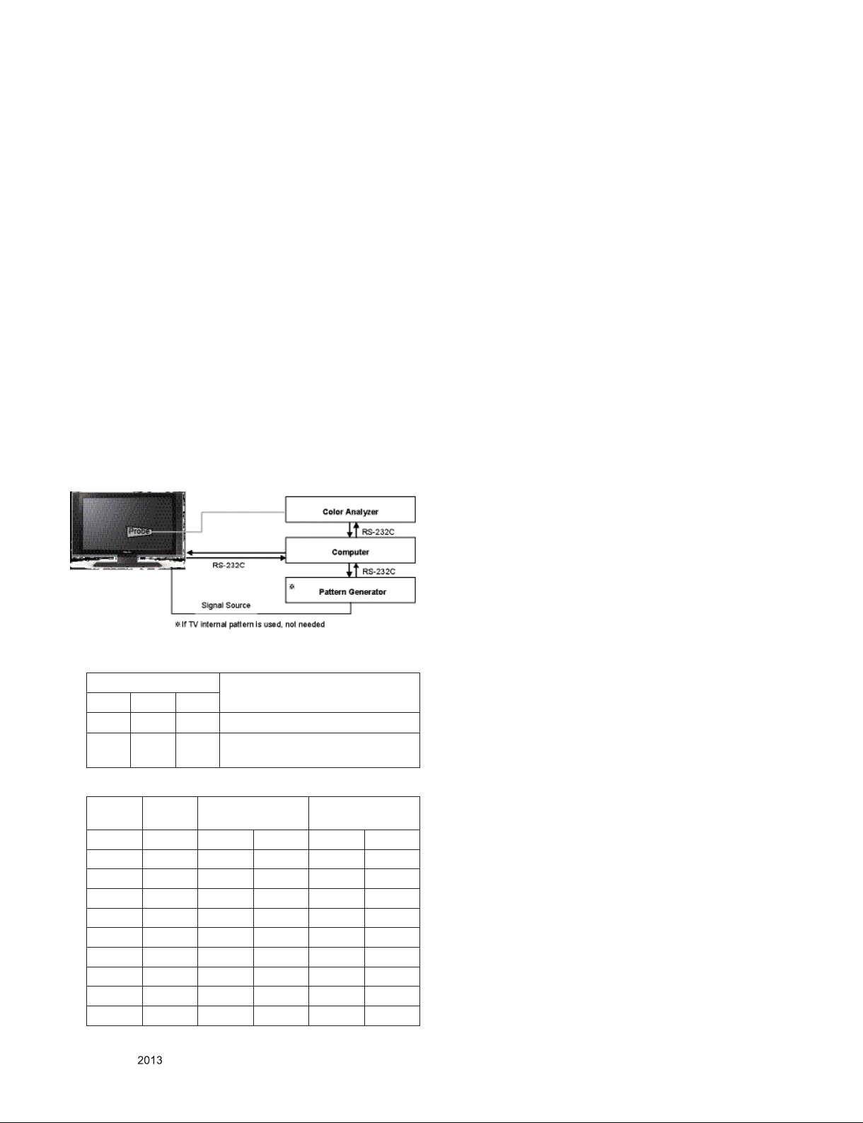
4.4. White Balance Adjustment
4.4.1. Overview
▪ W/B adj. Objective & How-it-works
(1) Objective: To reduce each Panel’s W/B deviation
(2) How-it-works: When R/G/B gain in the OSD is at 192, it
means the panel is at its Full Dynamic Range. In order to
prevent saturation of Full Dynamic range and data, one of
R/G/B is fixed at 192, and the other two is lowered to find
the desired value.
(3) Adj. condition: normal temperature
- Surrounding Temperature: 25±5 °C
- Warm-up time: About 5 Min
- Surrounding Humidity: 20% ~ 80%
4.4.2. Equipment
(1) Color Analyzer: CA-210 (NCG: CH 9 / WCG: CH12 / LED:
CH14)
(2) Adj. Computer (During auto adj., RS-232C protocol is
needed)
(3) Adjust Remocon
(4) Vi deo Signal Generator MSPG-925F 720p/204- Gray
(Model: 217, Pattern: 49)
※ Color Analyzer Matrix should be calibrated using CS-1000
4.4.3. Equipment connection
4.4.4. Adjustment Command (Protocol)
(1) RS-232C Command used during auto-adj.
RS-232C COMMAND
CMD DATA ID
Wb 00 00 Begin White Balance adj.
Wb 00 ff End White Balance adj.
(internal pattern disappears )
(2) Adjustment Map
Adj. item Command
(lower caseASCII)
CMD1 CMD2 MIN MAX
Cool R Gain j g 00 C0
G Gain j h 00 C0
B Gain j i 00 C0
Medium R Gain j a 00 C0
G Gain j b 00 C0
B Gain j c 00 C0
Warm R Gain j d 00 C0
G Gain j e 00 C0
B Gain j f 00 C0
Explanation
Data Range
(Hex.)
4.4.5. Adj. method
4.4.5.1. Auto adj. method
(1) Set TV in ADJ mode using P-ONLY key (or POWER ON
key)
(2) Place optical probe on the center of the display
- It need to check probe condition of zero calibration before
adjustment.
(3) Connect RS-232C Cable
(4) Select mode in ADJ Program and begin a adjustment.
(5) When WB adjustment is completed with OK message,
check adjustment status of pre-set mode (Cool, Medium,
Warm)
(6) Remove probe and RS-232C cable.
▪ W/B Adj. must begin as start command “wb 00 00” , and
finish as end command “wb 00 ff”, and Adj. offset if need
4.4.5.2. Manual adj. method
(1) Set TV in Adj. mode using POWER ON
(2) Zero Calibrate the probe of Color Analyzer, then place it on
the center of LCD module within 10cm of the surface..
(3) Press ADJ key -> EZ adjust using adj. R/C -> 9. White-
Balance then press the cursor to the right (KEY►). When
KEY(►) is pressed 216 Gray internal pa ttern will be
displayed.
(4) Adjust Cool modes
(i) Fix the one of R/G/B gain to 192 (default data) and
decrease the others. ( If G gain is adjusted over 172 and
R and B gain less than 192 , Adjust is O.K.)
(ii). If G gain is less than 172,
Increase G gain by up to 172, and then increase R gain
and G gain same amount of increasing G gain.
(iii) If R gain or B gain is over 255,
Readjust G gain less than 172, Conform to R gain is 255
or B gain is 255
(5) Adjust two modes (Medium / Warm) Fix the one of R/G/B
gain to 192 (default data) and decrease the others.
(6) Adj. is completed, Exit adjust mode using “EXIT” key on
Remote controller.
▪ If internal pattern is not available, use RF input. In EZ Adj.
menu 6.White Balance, you can select one of 2 Test-pattern:
ON, OFF. Default is inner (ON). By selecting OFF, you can
adjust using RF signal in 206 Gray pattern.
▪ Adj. condition and cautionary items
(1) Lighting condition in surrounding area
Surrounding lighting should be lower 10 lux. Try to isolate
adj. area into dark surrounding.
(2) Probe location: Color Analyzer (CA-210) probe should be
within 10cm and perpendicular of the module surface (80°~
100°)
(3) Aging time
- After Agi ng Sta rt, Keep the Power ON status during 5
Minutes.
- In case of LCD, Back-light on should be checked using no
signal or Full-white pattern.
Only for training and service purposes
- 15 -
LGE Internal Use OnlyCopyright © LG Electronics. Inc. All rights reserved.

※ CASE Cool
First adjust the coordinate far away from the target value(x, y).
(1) x, y >target
i) Decrease the R, G.
(2) x, y< target
i) First decrease the B gain,
ii) Decrease the one of the others.
(3) x > target , y < target
i) First decrease B, so make y a little more than the target.
ii) Adjust x value by decreasing the R
(4) x < target , y >target
i) First decrease B, so make x a little more than the target.
ii) Adjust x value by decreasing the G
How to adjust
(1) If G gain is adjusted over 172 and R gain and B gain less
than 192 , Adjust is O.K.
(2) If G gain is less than 172 , increase G gain by up to 172,
and then increase R gain and B gain same amount of
increasing G gain.
(3) If R gain or B gain is over 255 , Readjust G gain less than
172, Conform to R gain is 255 or B gain is 255
4.4.6. Reference (White Balance Adj. coordinate and
color temperature)
▪ Luminance: 204 Gray
▪ Standard color coordinate and temperature using CS-1000
(over 26 inch)
Mode
Cool 0.271 0.270 13,000K 0.0000
Medium 0.285 0.293 9,300K 0.0000
Warm 0.313 0.329 6,500K +0.0030
▪ S ta ndard col or coo rd ina te and tempe ratur e using
CA-210(CH 14)
Mode
Cool 0.269±0.002 0.273±0.002 13,000K 0.0000
Medium 0.285±0.002 0.293±0.002 9,300K 0.0000
Warm 0.313±0.002 0.329±0.002 6,500K 0.0000
Coordinate
X Y
Coordinate
X Y
Temp △uv
Temp △uv
※ CASE Medium / Warm
First adjust the coordinate far away from the target value(x, y).
(1) x, y > target
i) Decrease the R, G.
(2) x, y< target
i) First decrease the B gain,
ii) Decrease the one of the others.
(3) x >target , y< target
i) First decrease B, so make y a little more than the target.
ii) Adjust x value by decreasing the R
(4) x < target , y>target
i) First decrease B, so make x a little more than the target.
ii) Adjust x value by decreasing the G
▪ Adj. condition and cautionary items
(1) Lighting condition in surrounding area
Surrounding lighting should be lower 10 lux. Try to isolate
adj. area into dark surrounding.
(2) Probe location: Color Analyzer (CA-210) probe should be
within 10cm and perpendicular of the module surface (80°~
100°)
(3) Aging time
- After Agi ng Sta rt, Keep the Power ON status during 5
Minutes.
- In case of LCD, Back-light on should be checked using no
signal or Full-white pattern.
▪ S ta ndard col or coo rd ina te and tempe ratur e using
CA-210(CH-14) – by aging time
Normal Line(GAxxxx)
Cool Medium Warm
Aging time
GP4
(Min)
X Y X Y X Y
269 273 285 293 313 329
1 0-2 283 287 298 306 322 342
2 3-5 282 285 297 304 321 340
3 6-9 281 284 296 303 320 339
4 10-19 279 281 294 300 318 336
5 20-35 277 277 292 296 316 332
6 36-49 275 274 290 293 314 329
7 50-79 273 272 288 291 312 327
8 80-119 272 271 287 290 311 326
9 Over 120 271 270 286 289 310 325
Aging Chamber(GAxxxx)
Cool Medium Warm
Aging time
GP4
(Min)
X Y X Y X Y
269 273 285 293 313 329
1 0-5 282 285 297 304 321 340
2 6-10 278 280 293 299 317 335
3 11-20 275 275 290 294 314 330
4 21-30 272 272 287 291 311 327
5 31-40 269 269 284 288 308 324
6 41-50 268 267 283 286 307 322
7 51-80 267 266 282 285 306 321
8 81-119 266 264 281 283 305 319
9 Over 120 265 263 280 282 304 318
Only for training and service purposes
- 16 -
LGE Internal Use OnlyCopyright © LG Electronics. Inc. All rights reserved.
4.5. Option selection per country
4.5.1. Overview
(1) Press ADJ key on the Adj. R/C, and then select Country
Group Menu.
(2) Depending on destination, select KR or US, then on the
lower Country option, select US, CA, MX. Selection is done
using +, - KEY
4.6. Tool Option Inspection
▪ Method: Press Adj. key on the Adj. R/C, then select Tool option.
Model Tool 1 Tool 2 Tool 3 Tool 4 Tool 5 Tool 6 Tool 7
47GA6400-UD 33207 8723 30512 13356 18441 1322 13963
42GA6400-UD 33206 8723 30512 13356 18441 1322 13963
4.7. Local Dimming Inspection (Optional)
(1) Press ‘TILT” key of the Adj. R/C and check movin g
patterns. The black bar patterns moves from top to bottom.
If a local dimming function does not work, a whole screen
shows full white
5. GND and Internal Pressure check
5.1. Method
(1) GND & Internal Pressure auto-check preparation
- Check that Power Cord is fully inserted to the SET.
(If loose, re-insert)
(2) Perform GND & Internal Pressure auto-check
- Unit fully inserted Power cord; Antenna cable and A/V
arrive to the auto-check process.
- Connect D-terminal to AV JACK TESTER
- Auto CONTROLLER (GWS103-4) ON
- Perform GND TEST
- If NG, Buzzer will sound to inform the operator.
- If OK, changeover to I/P check automatically.
(Remove CORD, A/V form AV JACK BOX)
- Perform I/P test
- If NG, Buzzer will sound to inform the operator.
- If OK, Good lamp will lit up and the stopper will allow the
pallet to move on to next process.
5.2. Checkpoint
(1) Test voltage
- GND: 1.5KV/min at 100mA
- SIGNAL: 3KV/min at 100mA
(2) TEST time: 1 second
(3) TEST POINT
- GND Test = POWER CORD GND and SIGNAL CABLE
GND.
- Hi-pot Test = POWER CORD GND and LIVE & NEUTRAL.
(4) LEAKAGE CURRENT: At 0.5mArms
4.8. Ship-out mode check (In-stop)
▪ After final inspection, press In-Stop key of the Adj. R/C and
check that the unit goes to Stand-by mode.
▪ After final inspection, Always turn on the Mechanical S/W.
4.9. WIFI MAC ADDRESS CHECK
a. Using RS232
Command Set ACK
Transmission [A][l][][Set ID][][20][Cr] [O][K][x] or [N][G]
b. check the menu on in-start
Note that there are Wi-Fi MAC and MAC address.
Wi-Fi MAC is used for wireless network and MAC address is used
for wired network
6. EYE-Q Operation check
Step 1) Turn on the TV..
Step 2) Press ' EY E button' o n t he adjustm en t remote -
controller.
Step 3) Cover 'Eye Q sensor' on the front of set with your
hands, hold it for 6 seconds.
Step 4) Check "the Sensor Data" on the screen, make certain
that Data is below 10. If Data isn’t below 10 in 6
seconds, Eye Q sensor would be bad. You should
change Eye Q sensor.
Step 5) Uncover your hands from Eye Q sensor, hold it for 6
seconds.
Step 6) Check "Back Light(xxx)" on the screen, check data
increase . You should change Eye Q sensor.
<Step 2>
<Step 4>
<Step 3>
<Step 5>
<Step 6>
Only for training and service purposes
- 17 -
LGE Internal Use OnlyCopyright © LG Electronics. Inc. All rights reserved.
7. QWERTY Remote Control Inspection
- Requ ired Ins trument s: Ins pection RF-re mote con trol,
Inspection IR-KEY-CODE remote control.
- Prior to the test, AA battery for the RF-remote control should
be a de qu at e. C ha ng e th e batte ry for each LO T is
recommended)
- Test procedures
(1) Press the ‘START’ key on the controller to pair with the
set.
(2) Press the ‘OK’ key in the controller and check whether
the cursor appears on the set.
(3) Press ‘Vol+ (STOP)’ key to de-pair with the set.
8. Audio
No Item Min Typ Max Unit Remark
1 Audio
practical
max Output,
L/R
2 Speaker
(8Ω Impedance)
Measurement condition:
(1) RF input: Mono, 1 KHz sine wave signal, 100% Modulation
(2) CVBS, Component: 1 KHz sine wave signal 0.4Vrms
(3) RGB PC: 1 KHz sine wave signal 0.7Vrms
9.0 10.0 12.0 W Measurement
condition
(TBD)
8.5 8.9 9.8 Vrms
10.0 15.0 W Measurement
condition
(TBD)
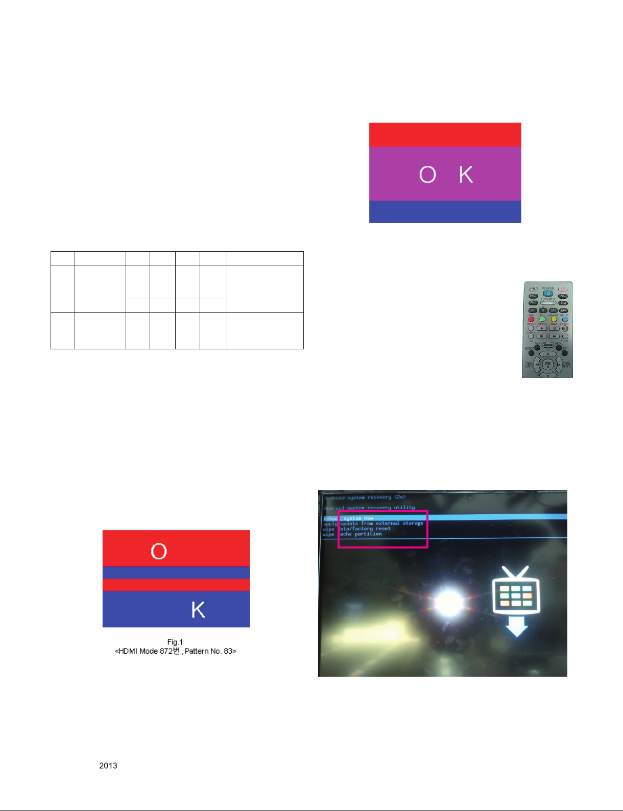
(2) Press ‘OK” key as a 3D input OSD is shown.
(3) Check pattern as Fig2 without 3D glasses. (3D mode
without 3D glasses)
Fig.2
<OK in 3D mode without 3D glasses>
10. IR Blaster Function Test
10.1. Test equipment
(1) IR Blaster Jig
(2) Test Mode : Power Only Mode
10.2 Test method
(1) Input IR Blaster Jig to IR Blaster Phone Jack
(2) Press MPX Key
(3) Checked LED Lighting of IR Blaster Jig.
9. 3D function test
9.1 Test equipment
(1) Pattern Generator MSHG-600 or MSPG-6100 (HDMI 1.4
support)
(2) Pattern: HDMI mode (model No. 872, pattern No. 83)
9.2 Test method
(1) Input 3D test signal as Fig.1.
11. USB S/W Download
(optional, Service only)
(1) Make the TV’s status to DC off
(2) Make the download file’s name to “lg_ota.zip “ and save it
on USB root.
(3) Put the USB Stick to the USB No.1
(4) Press “B-tooth” key during 3~4 second.
(5) Updating Completed, The TV will restart automatically
Only for training and service purposes
- 18 -
* After downloading, TOOL OPTION setting is needed again.
(1) Push "IN-START" key in service remote controller.
(2) Select "Tool Option 1" and Push “OK” button.
(3) Punch in the number. (Each model has their number.)
LGE Internal Use OnlyCopyright © LG Electronics. Inc. All rights reserved.

12. Optional adjustments
12.1. Manual ADC Calibration
12.1.1. Equipment & Condition
(1) Adjustment Remocon
(2) 801GF (802B , 80 2F, 802R) or MSPG925FA Pat tern
Generator
- Resolution : 4 80 i Com p1 ( MSP G- 925 FA : m ode l- 209 ,
pattern-65)
- Resolution : 1080p Comp1 ( MSPG-925FA: model-225,
pattern-65)
- Resolution : 1 080 p RGB ( MSP G-9 2 5FA: m o del -22 5,
pattern-65)
- Pattern : Horizontal 100% Color Bar Pattern
- Pattern level : 0.7±0.1 Vp-p
12.1.2. Adjust method
12.1.2.1 ADC 480i/1080p Comp1, RGB
(1) Check connected condition of Comp1/RGB cable to the
equipment
(2) Give a 480i Mode, Horizontal 100% Color Bar Pattern to
Comp1. (MSPG-925FA -> Model: 209, Pattern: 65)
(3) Change input mode as Component1 and picture mode as
“Standard”
(4) Press the In-start Key on the ADJ remote after at least 1
min of signal reception. Then, select 7.External ADC. And
Press OK or Right Button for going to sub menu.
(5) Press OK in Comp 480i menu
(6) Give a 1080p Mode, Horizontal 100% Color Bar Pattern to
Comp1. (MSPG-925FA -> Model: 225, Pattern: 65)
(7) Press OK in Comp 1080p menu
(8) Perform (6) and (7) in RGB-PC
(9) If ADC Comp is successful, “ADC Component Success” is
displayed. If ADC calibration is failure, “ADC Component
Fail” is displayed.
(10) If ADC calibration is failure, after rechecking ADC pattern
or condition, retry calibration
(11) If ADC RG B cali br ation is succe ssful, “ ADC RGB
Success” is displayed. If ADC calibration is failure, “ADC
RGB Fail” is displayed.
(12) If ADC calibration is failure, after recheck ADC pattern or
condition, retry calibration
12.2. Manual White balance Adjustment
12.2.1. Adj. condition and cautionary items
(1) Lighting condition in surrounding area surrounding lighting
should be lower 10 lux. Try to isolate adj. area into dark
surrounding.
(2) Probe location: Color Analyzer (CA-210) probe should be
within 10cm and perpendicular of the module surface
(80°~ 100°)
(3) Aging time
▪ After Aging Start, Ke ep the Po wer ON status during 5
Minutes.
▪ In case of LCD, Back-light on should be checked using no
signal or Full-white pattern.
12.2.2. Equipment
(1) Color Analyzer: CA-210 (NCG: CH 9 / WCG: CH12 / LED:
CH14)
(2) Adj. Computer (During auto adj., RS-232C protocol is
needed)
(3) Adjust Remocon
(4) Vi deo Sig nal Generator MSP G-925F 720p/216 -Gray
(Model: 217, Pattern: 78)
12.2.3. Adjustment
(1) Set TV in Adj. mode using POWER ON
(2) Zero Calibrate the probe of Color Analyzer, then place it on
the center of LCD module within 10cm of the surface.
(3) Press ADJ key -> EZ adjust using adj. R/C -> 6. White-
Balance then press the cursor to the right (KEY►).
When KEY(►) is pressed 216 Gray internal pattern will be
displayed.
(4) One of R Gain / G Gain / B Gain should be fixed at 192,
and the rest will be lowered to meet the desired value.
(5) Adj. is performed in COOL, MEDIUM, WARM 3 modes of
color temperature.
▪ If internal pattern is not available, use RF input. In EZ Adj.
menu 6.White Balance, you can select one of 2 Test-pattern:
ON, OFF. Default is inner(ON). By selecting OFF, you can
adjust using RF signal in 216 Gray pattern.
Only for training and service purposes
- 19 -
LGE Internal Use OnlyCopyright © LG Electronics. Inc. All rights reserved.
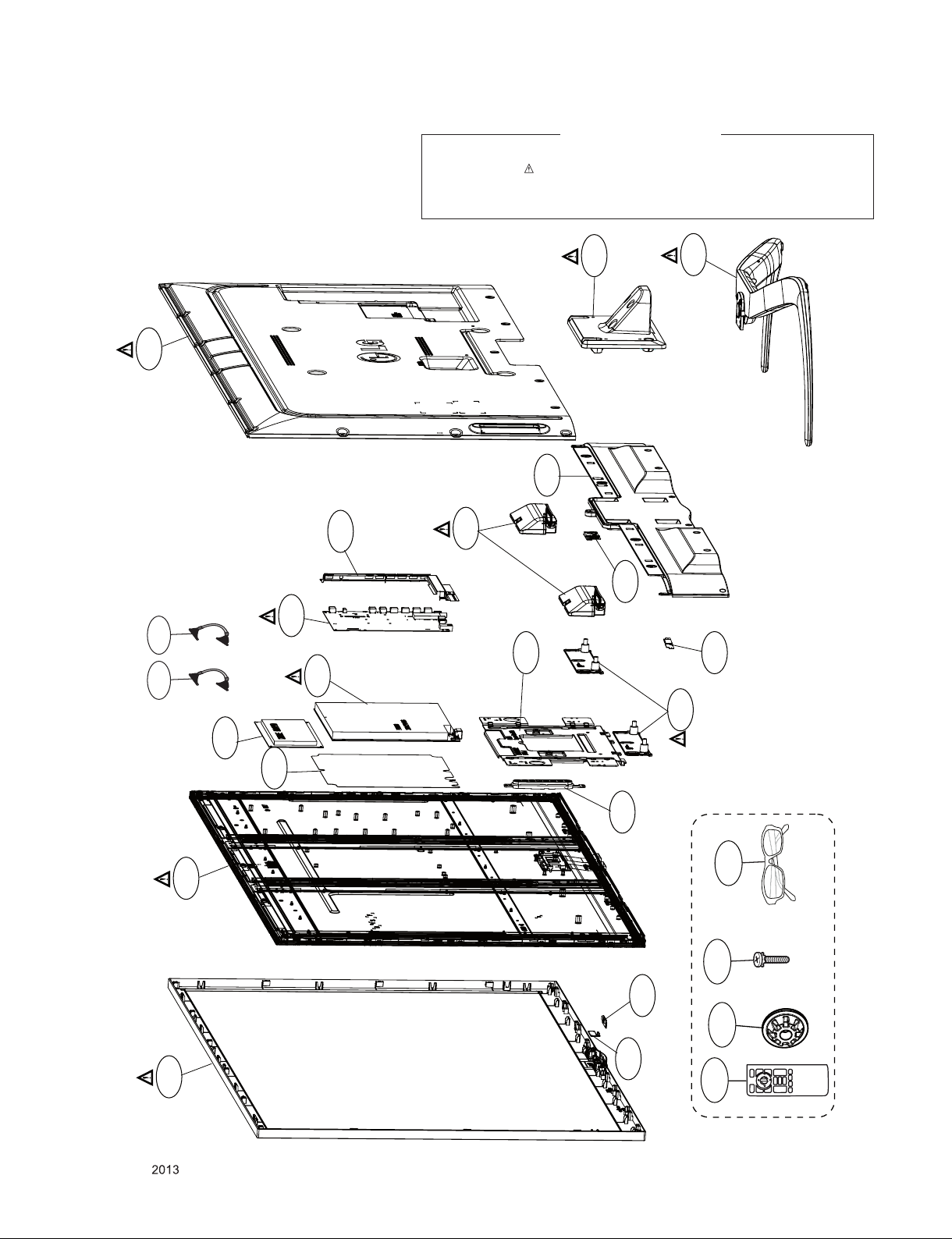
EXPLODED VIEW
IMPORTANT SAFETY NOTICE
Many electrical and mechanical parts in this chassis have special safety-related characteristics. These
parts are identified by in the Schematic Diagram and EXPLODED VIEW.
It is essenti al that these special safet y parts shoul d be replac ed with the same compo nents as
recommended in this manual to prevent X-RADIATION, Shock, Fire, or other Hazards.
Do not modify the original design without permission of manufacturer.
910
900
400
410
521
120
570
540
810
LV1 LV2
530
560
200L
200
300
Only for training and service purposes
122
800
510
AG1
A10
* Set + Stand
500
* Stand Base + Body
A7
580
A2
- 20 -
LGE Internal Use OnlyCopyright © LG Electronics. Inc. All rights reserved.
System Configuration
Copyright ⓒ 2013 LG Electronics. Inc. All right reserved.
Only for training and service purposes
LGE Internal Use Only
NVRAM
Clock for LG1152
MAIN Clock(24Mhz)
C100
8pF
50V
X-TAL_1
GND_1
1
2
X101
24MHz
4
3
C101
8pF
50V
GND_2
X-TAL_2
PLL SET[1:0] ==> Internal Pull-UP. N.C is high
00 : CPU clock(1056Mhz), Main0,1/2 DDR (792/792 Mhz)
01 : CPU clock(792Mhz), Main0,1/2 DDR (672/792 Mhz)
10 : CPU clock(1152Mhz), Main0,1/2 DDR (792/672 Mhz)
11 : CPU clock(984Mhz), Main0,1/2 DDR (792/792 Mhz)
BOOT MODE
"11" or "01" : NOR
"10" : eMMC
"00" : NAND
OPT
R102 22
R103 22
OPT
PLLSET1
PLLSET0
R112
XIN_MAIN
1M
XO_MAIN
JTAG I/F FOR MAIN
+3.3V_NORMAL
+3.3V_NORMAL
4.7K
R187
BOOT_MODE1
4.7K
R185
OPT
BOOT_MODE1
+3.3V_NORMAL
4.7K
R188
OPT
4.7K
R186
BOOT_MODE0
TRST_N0
TDI0
TDO0
TMS0
TCK0
SOC_RESET
OPT
OPT
R132 10K
R131 10K
OPT
OPT
R133 10K
R134 10K
BOOT_MODE0
+3.3V_NORMAL
NO_FRC
Zoran FRC
(For UD)
MODEL OPTION 8 is just for CP Box
It should not be appiled at MP
HW_OPT_0
HW_OPT_1
HW_OPT_2
HW_OPT_3
HW_OPT_4
HW_OPT_5
HW_OPT_6
HW_OPT_7
HW_OPT_8
HW_OPT_9
HW_OPT_10
HP_AMP_MUTE
BackEnd 1
BackEnd 2
Pannel Resol
OPTIC I/F
3D Depth IC
DDR Size
CP BOX
FrontEnd 1
FrontEnd 2
OPT
22
R117
10K
URSA5
R110
FRC_EXTERNAL
R100 10K
10K
FRC3
FRC_INTERNAL
R107 10K
R111
T240
T120
OPT
OPTIC
R138 10K
R124 10K
3D_DEPTH
R140 10K
CP_BOX
R145 10K
R152 10K
R147 10K
DVB_T2_TUNER
DVB_S_TUNER
R156 10K
R154 10K
DVB_C2_TUNER
ZORAN_FRC
R121 10K
MODEL_OPT_0
MODEL_OPT_1
MODEL_OPT_2
MODEL_OPT_3
MODEL_OPT_4
MODEL_OPT_5
MODEL_OPT_6
MODEL_OPT_7
MODEL_OPT_8
MODEL_OPT_9
MODEL_OPT_10
1GByte
NON_OPTIC
R139 10K
R125 10K
R141 10K
R146 10K
NON_3D DEPTH
NON_CP_BOX
R153 10K
R148 10K
NON_DVB_T2_TUNER
R158 10K
R155 10K
NON_DVB_S_TUNER
NON_DVB_C2_TUNER
NOT_ZORAN_FRC
R126 10K
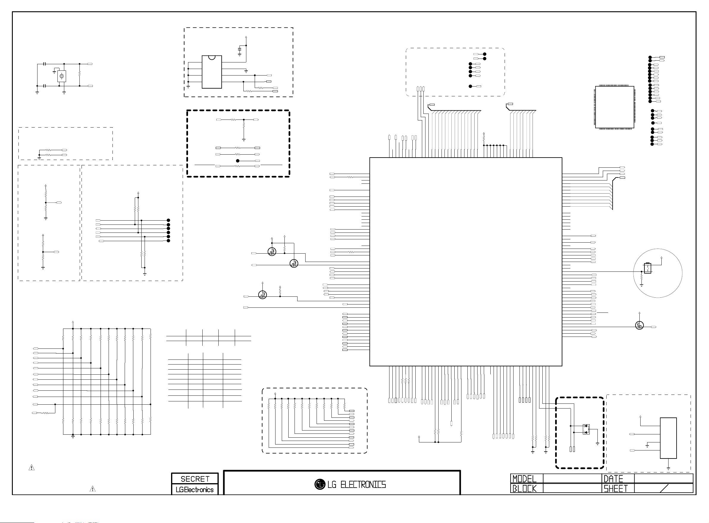
THE SYMBOL MARK OF THIS SCHEMETIC DIAGRAM INCORPORATES
SPECIAL FEATURES IMPORTANT FOR PROTECTION FROM X-RADIATION.
FILRE AND ELECTRICAL SHOCK HAZARDS, WHEN SERVICING IF IS
ESSENTIAL THAT ONLY MANUFATURES SPECFIED PARTS BE USED FOR
THE CRITICAL COMPONENTS IN THE SYMBOL MARK OF THE SCHEMETIC.
IC102
R1EX24256BSAS0A
A0
1
A1
A2
VSS
8
2
7
A0’h
3
6
4
5
Place to LVDS Wafer
TCON_I2C_EN
SoC
internal
FRC
0
0 1
1
HIGH
FHD
OPTIC
3D DEPTH
3D_Depth_IC
DDR Reserved
CP BOX
Enable
T2 Tuner
Support
S Tuner
Support
Support
C2 Tuner
Support
C111
0.1uF
VCC
WP
SCL
SDA
G3S
R151 22
R160 22
R162 22
R116
1/16W 5%
G3S
MHL_DET
HDMI_INT
LG FRC3
10
0
LOW
UD
NON_OPTIC
NON_3D_Depth_IC
DDR_Default
Disable
Not Support
Not Support
Not Support
Not Support
+3.3V_NORMAL
Write Protection
- Low : Normal Operation
- High : Write Protection
R143
OPT
22
10K
G3S
R170
0
SOC_RX
SOC_TX
2N7002K
URSA5
1
R142
OPT
22
TCON_I2C
I2C_BE_SDA1I2C_SDA1
I2C_BE_SCL1I2C_SCL1
LOCAL_DIM_EN
T-CON_EEPROM_WPTCON_EEPROM_WP
2N7002K
+5V_NORMAL
G
D
Q105
R178
I2C_SCL5
I2C_SDA5
+5V_NORMAL
G
D
Q100
+3.3V_NORMAL
S
OPT
+3.3V_NORMAL
2.2K
R179
2.2K
I2C_SCL3
I2C_SDA3
+3.3V_NORMAL
S
OPT
R203
100K
R181
R180
3.3K
R202
100K
D
Q103
2N7002K
3.3K
R182
G
2.2K
S
M_REMOTE_RX
M_REMOTE_TX
IRB_SPI_MISO
IRB_SPI_MOSI
IRB_SPI_CK
IRB_SPI_SS
AV1_CVBS_DET
I2C PULL UP
R197
R196
3.3K
R195
2.2K
XIN_MAIN
XO_MAIN
SOC_RESET
TRST_N0
TMS0
TCK0
TDI0
TDO0
PLLSET1
PLLSET0
BOOT_MODE1
BOOT_MODE0
EPHY_INT
/USB_OCD2
/USB_OCD3
UART1_RX
UART1_TX
DTV_ATV_SELECT
3.3K
R198
3.3K
I2C_SCL1
I2C_SDA1
I2C_SCL2
I2C_SDA2
I2C_SCL3
I2C_SDA3
I2C_SCL4
I2C_SDA4
I2C_SCL5
I2C_SDA5
I2C_SCL6
I2C_SDA6
R199
3.3K
R101 22
R184
R183
1.2K
R104 560
1%
BOOT_MODE1
BOOT_MODE0
1.2K
I2C_SDA1
I2C_SCL1
I2C_SDA2
I2C_SCL2
I2C_SDA3
I2C_SCL3
I2C_SDA4
I2C_SCL4
I2C_SDA5
I2C_SCL5
I2C_SDA6
I2C_SCL6
A22
XIN_MAIN
B22
XO_MAIN
AB16
OPM1
AB17
OPM0
AE3
PORES_N
V23
TRST_N0
U25
TMS0
V25
TCK0
V24
TDI0
U24
TDO0
Y22
TRST_N1
AA22
TMS1
AB20
TCK1
AB21
TDI1
W22
TDO1
AB9
PLLSET1
AB8
PLLSET0
AB15
BOOT_MODE1
AB14
BOOT_MODE0
Y23
EXT_INTR3/GPIO48
W25
EXT_INTR2/GPIO63
W24
EXT_INTR1/GPIO62
W23
EXT_INTR0/GPIO61
Y5
UART0_RX/GPIO49
W6
UART0_TX/GPIO50
AA6
UART1_RX
Y6
UART1_TX
AB5
UART2_RX
AA5
UART2_TX
AB23
SPI_DI0/GPIO39
AB24
SPI_DO0/GPIO38
AA25
SPI_SCLK0/GPIO37
AB25
SPI_CS0/GPIO36
Y25
SPI_DI1/GPIO35
AA23
SPI_DO1/GPIO34
Y24
SPI_SCLK1/GPIO33
AA24
SPI_CS1/GPIO32
AB6
SCL0/GPIO60
AB4
SDA0/GPIO59
AC5
SCL1/GPIO58
AC4
SDA1/GPIO57
AD4
SCL2/GPIO56
AE4
SDA2/GPIO71
AE5
SCL3/GPIO70
AD5
SDA3/GPIO69
AE6
SCL4/GPIO68
AD6
SDA4/GPIO67
AC6
SCL5/GPIO66
AC7
SDA5/GPIO65
USB_CTL3
FPGA_LVDS_INFO
M25
M24
M23
N23
T27
EB_CS3/GPIO64
EB_CS2/GPIO79
EB_CS1/GPIO78
EB_CS0/GPIO77
RMII_REF_CLK
RMII_CRS_DV
RMII_MDIO
RMII_MDC
AD2
AB1
AB2
AB3
AC2
R105 22
EPHY_MDC
EPHY_MDIO
EPHY_REFCLK
EPHY_CRS_DV
for DiiVA(China)
SEL_USB1
SEL_USB2
SEL_USB3
EB_ADDR[0-14]
EB_ADDR[9]
EB_ADDR[8]
EB_ADDR[12]
EB_ADDR[13]
EB_ADDR[14]
EB_ADDR[10]
EB_OE_N
EB_WE_N
T28
U27
EB_OE_N
EB_WE_N
EB_BE_N1
U26
U28
EB_WAIT
EB_BE_N1
EB_BE_N0
J22
EB_BE_N0
EB_ADDR[11]
K22
J23
L26
L27
L25
N26
EB_ADDR14
EB_ADDR13
EB_ADDR12
EB_ADDR17/GPIO84
EB_ADDR16/GPIO83
EB_ADDR15/GPIO82
N27
M26
L28
EB_ADDR9
EB_ADDR11
EB_ADDR10
IC100
LG1152D-B1
LG1152_NON_RM
RMII_TXEN
RMII_TXD1
RMII_TXD0
RMII_RXD1
RMII_RXD0
CAM_CE1_N
CAM_CE2_N
CAM_CD1_N
CAM_CD2_N
CAM_VS1_N
CAM_VS2_N
CAM_IREQ_N
CAM_RESET
CAM_INPACK_N
AC3
AE1
AD3
AD1
W26
V28
Y27
Y26
W28
W27
AA28
AB26
AA27
AA26
R108 22
R106 22
EPHY_EN
EPHY_TXD1
EPHY_RXD0
EPHY_TXD0
EPHY_RXD1
+3.3V_NORMAL
/PCM_CE2
/PCM_CE1
CAM_CD2_N
CAM_CD1_N
CI
10K
R166
R167 10K
CAM_IREQ_N
CI
PCM_RST
CAM_INPACK_N
EPHY_INT
EB_ADDR[4]
EB_ADDR[7]
EB_ADDR[5]
EB_ADDR[6]
L24
L23
K28
EB_ADDR8
EB_ADDR7
EB_ADDR6
EB_ADDR5
CAM_VCCEN_N
CAM_WAIT_N
CAM_REG_N
CAM_IOIS16_N
Y28
V27
V26
CAM_REG_N
CAM_WAIT_N
CI
10K
R168
PCM_5V_CTL
HP_DET
EB_ADDR[3]
EB_ADDR[2]
EB_ADDR[1]
K27
K26
K25
EB_ADDR4
EB_ADDR3
EB_ADDR2
SC_CLK/GPIO90
SC_DETECT/GPIO93
R25
U23
SMARTCARD_DET
SMARTCARD_CLK
SEL_USB1
SEL_USB2
SEL_USB3
/RST_PHY
SC_DET
EB_ADDR[0]
+3.3V_NORMAL
10K
R109
K24
K23
V22
U22
EB_ADDR1
EB_ADDR0
EB_DATA15
SC_VCCEN/GPIO89
SC_VCC_SEL/GPIO88
SC_RST/GPIO91
SC_DATA/GPIO92
T25
T24
T23
R24
SMARTCARD_RST
SMARTCARD_VCC
SMARTCARD_DATA
SMARTCARD_PWR_SEL
T22
R22
P22
N22
EB_DATA14
EB_DATA13
EB_DATA12
EB_DATA11
EB_DATA10
SD_CLK/GPIO76
SD_CMD/GPIO73
SD_CD_N/GPIO75
SD_WP_N/GPIO74
C22
C23
A23
B23
MOTOR_CLOSE_SW
MO_SENS_TO_MAIN_UP
MO_SENS_TO_MAIN_DOWN
EB_DATA[0-7]
EB_DATA[7]
EB_DATA[4]
EB_DATA[3]
EB_DATA[6]
EB_DATA[2]
EB_DATA[1]
EB_DATA[5]
EB_DATA[0]
M22
L22
T26
R28
R27
R26
P28
P27
P26
N28
EB_DATA9
EB_DATA8
EB_DATA7
EB_DATA6
EB_DATA5
EB_DATA4
EB_DATA3
EB_DATA2
EB_DATA1
EB_DATA0
SD_DATA3/GPIO72
SD_DATA2/GPIO87
SD_DATA1/GPIO86
SD_DATA0/GPIO85
USB_DP1
USB_DM1
USB_DP2
USB_DM2
USB_TXR_RKL
USB_ANALOGTEST
BT_USB_DP
BT_USB_DM
A24
B24
C24
A25
B27
A27
A26
B26
C25
B25
AA1
AA2
USB_DM3
USB_DP3
USB_HUB_IC_IN_DM
USB_HUB_IC_IN_DP
22
OPT
R173
R174
MOTOR_CW
MOTOR_CCW
IR_B_RESET
MOTOR_OPEN_SW
Place near Jack side
EMMC_RST
EMMC_CLK
EMMC_CMD
EMMC_DATA7
EMMC_DATA6
EMMC_DATA5
EMMC_DATA4
EMMC_DATA3
EMMC_DATA2
EMMC_DATA1
EMMC_DATA0
NAND_CS1
NAND_CS0
NAND_ALE
NAND_CLE
NAND_REN
NAND_WEN
GPIO31
GPIO30
GPIO29
GPIO28
GPIO27
GPIO26
GPIO25
GPIO24
GPIO23
GPIO22
GPIO21
GPIO20
GPIO19
GPIO18
GPIO17
GPIO16
GPIO15
GPIO14
GPIO13
GPIO12
GPIO11
GPIO10
GPIO9
GPIO8
GPIO7
GPIO6
GPIO5
GPIO4
GPIO3
GPIO2
GPIO1
GPIO0
BT_TXR_RKL
BT_ANALOGTEST
Y4
AA4
22
OPT
R175
R176
LG1152 B1
E28
F27
F26
C26
EMMC_DATA[7]
E27
EMMC_DATA[6]
E26
EMMC_DATA[5]
D27
EMMC_DATA[4]
D28
EMMC_DATA[3]
C27
EMMC_DATA[2]
C28
EMMC_DATA[1]
D26
EMMC_DATA[0]
R23
P24
N25
P23
N24
P25
AC1
V7
W5
W4
V6
V5
V4
U6
U5
U4
T6
T5
T4
R6
R5
R4
P6
P5
P4
N6
N5
N4
N3
M6
AC23
AC24
AE24
AD23
AE23
AC22
AD22
AE22
WIFI_DP
WIFI_DM
MAIN & GPIO
A22
XIN_MAIN
B22
XO_MAIN
AB16
OPM1
AB17
OPM0
AE3
PORES_N
V23
TRST_N0
U25
TMS0
V25
TCK0
V24
TDI0
U24
TDO0
Y22
TRST_N1
AA22
TMS1
AB20
TCK1
AB21
TDI1
W22
TDO1
AB9
PLLSET1
AB8
PLLSET0
AB15
BOOT_MODE1
AB14
BOOT_MODE0
Y23
EXT_INTR3/GPIO48
W25
EXT_INTR2/GPIO63
W24
EXT_INTR1/GPIO62
W23
EXT_INTR0/GPIO61
Y5
UART0_RX/GPIO49
W6
UART0_TX/GPIO50
AA6
UART1_RX
Y6
UART1_TX
AB5
UART2_RX
AA5
UART2_TX
AB23
SPI_DI0/GPIO39
AB24
SPI_DO0/GPIO38
AA25
SPI_SCLK0/GPIO37
AB25
SPI_CS0/GPIO36
Y25
SPI_DI1/GPIO35
AA23
SPI_DO1/GPIO34
Y24
SPI_SCLK1/GPIO33
AA24
SPI_CS1/GPIO32
AB6
SCL0/GPIO60
AB4
SDA0/GPIO59
AC5
SCL1/GPIO58
AC4
SDA1/GPIO57
AD4
SCL2/GPIO56
AE4
SDA2/GPIO71
AE5
SCL3/GPIO70
AD5
SDA3/GPIO69
AE6
SCL4/GPIO68
AD6
SDA4/GPIO67
AC6
SCL5/GPIO66
AC7
SDA5/GPIO65
LG1152_RM
IC100-*1
OPTIC_FPGA_RESET
OPTIC_SERDES_RESET
/RST_PHY
OLED_TCON_RESET
HW_OPT_9
SC_DET
COMP1_DET
HW_OPT_5
HW_OPT_6
HW_OPT_10
M_RFModule_RESET
FRC_RESET
HW_OPT_2
HW_OPT_1
HW_OPT_0
HW_OPT_4
FLASH_WP
/RST_HUB
HW_OPT_3
OPT
RCLAMP0502BA
D100
M25
M24
M23
N23
T27
T28
U27
U26
U28
J22
K22
J23
L26
L27
L25
N26
N27
M26
L28
EB_OE_N
EB_WE_N
EB_WAIT
EB_BE_N1
EB_BE_N0
EB_ADDR9
EB_ADDR14
EB_ADDR13
EB_ADDR12
EB_ADDR11
EB_ADDR10
EB_CS3/GPIO64
EB_CS2/GPIO79
EB_CS1/GPIO78
EB_CS0/GPIO77
EB_ADDR17/GPIO84
EB_ADDR16/GPIO83
EB_ADDR15/GPIO82
RMII_REF_CLK
RMII_CRS_DV
RMII_MDIO
RMII_MDC
RMII_TXEN
RMII_TXD1
RMII_TXD0
RMII_RXD1
RMII_RXD0
CAM_CE1_N
CAM_CE2_N
CAM_CD1_N
CAM_CD2_N
CAM_VS1_N
CAM_VS2_N
CAM_IREQ_N
CAM_RESET
CAM_INPACK_N
AD2
AB1
AB2
AB3
AC2
AC3
AE1
AD3
AD1
W26
V28
Y27
Y26
W28
W27
AA28
AB26
AA27
AA26
HW_OPT_7
HW_OPT_8
HP_DET
RF_SWITCH_CTL
/TU_RESET1
/S2_RESET
L24
L23
K28
EB_ADDR8
EB_ADDR7
EB_ADDR6
CAM_VCCEN_N
CAM_WAIT_N
CAM_REG_N
Y28
V27
V26
K27
K26
K25
K24
K23
EB_ADDR5
EB_ADDR4
EB_ADDR3
EB_ADDR2
EB_ADDR1
EB_ADDR0
CAM_IOIS16_N
SC_CLK/GPIO90
SC_DETECT/GPIO93
SC_VCCEN/GPIO89
SC_VCC_SEL/GPIO88
R25
U23
T25
T24
UART1_RX
V22
U22
T22
R22
P22
N22
M22
L22
T26
R28
R27
EB_DATA9
EB_DATA8
EB_DATA7
EB_DATA6
EB_DATA15
EB_DATA14
EB_DATA13
EB_DATA12
EB_DATA11
EB_DATA10
SC_RST/GPIO91
SC_DATA/GPIO92
SD_CLK/GPIO76
SD_CMD/GPIO73
SD_CD_N/GPIO75
SD_WP_N/GPIO74
SD_DATA3/GPIO72
SD_DATA2/GPIO87
SD_DATA1/GPIO86
SD_DATA0/GPIO85
T23
R24
C22
C23
A23
B23
A24
B24
C24
A25
UART1_TX
R26
EB_DATA5
P28
P27
P26
N28
EB_DATA4
EB_DATA3
EB_DATA2
EB_DATA1
EB_DATA0
E28
EMMC_RST
F27
EMMC_CLK
F26
EMMC_CMD
C26
EMMC_DATA7
E27
EMMC_DATA6
E26
EMMC_DATA5
D27
EMMC_DATA4
D28
EMMC_DATA3
C27
EMMC_DATA2
C28
EMMC_DATA1
D26
EMMC_DATA0
R23
NAND_CS1
P24
NAND_CS0
N25
NAND_ALE
P23
NAND_CLE
N24
NAND_REN
P25
NAND_WEN
AC1
GPIO31
V7
GPIO30
W5
GPIO29
W4
GPIO28
V6
GPIO27
V5
GPIO26
V4
GPIO25
U6
GPIO24
U5
GPIO23
U4
GPIO22
T6
GPIO21
T5
GPIO20
T4
GPIO19
R6
GPIO18
R5
GPIO17
R4
GPIO16
P6
GPIO15
P5
GPIO14
P4
GPIO13
N6
GPIO12
N5
GPIO11
N4
GPIO10
N3
GPIO9
M6
GPIO8
AC23
GPIO7
AC24
GPIO6
AE24
GPIO5
AD23
GPIO4
AE23
GPIO3
AC22
GPIO2
AD22
GPIO1
AE22
GPIO0
USB_DP1
USB_DM1
USB_DP2
USB_DM2
USB_TXR_RKL
USB_ANALOGTEST
BT_USB_DP
BT_USB_DM
BT_TXR_RKL
BT_ANALOGTEST
Y4
B27
A27
A26
B26
C25
B25
AA1
AA2
AA4
EMMC_RST
EMMC_CLK
EMMC_CMD
EMMC_DATA[0-7]
JTP-1127WEM
1/16W
5%
+5V_NORMAL
S
Q104
2N7002K
Debug
+3.3V_NORMAL
+3.3V_NORMAL
SW1
4 3
R201
2.7K
G
D
1
SMARTCARD_DATA
SMARTCARD_RST
SMARTCARD_PWR_SEL
SMARTCARD_VCC
SMARTCARD_DET
SMARTCARD_CLK
MOTOR_CLOSE_SW
MOTOR_OPEN_SW
MOTOR_CW
MOTOR_CCW
MO_SENS_TO_MAIN_UP
MO_SENS_TO_MAIN_DOWN
12
For ISP
Delete PV
DEBUG
HDMI_S/W_RESET
12507WS-04L
I2C_SDA2
I2C_SCL2
OPTIC_FPGA_RESET
OPTIC_SERDES_RESET
OLED_TCON_RESET
FPGA_LVDS_INFO
IRB_SPI_MISO
IRB_SPI_MOSI
IRB_SPI_CK
IRB_SPI_SS
IR_B_RESET
P100
1
DEBUG
2
3
4
5
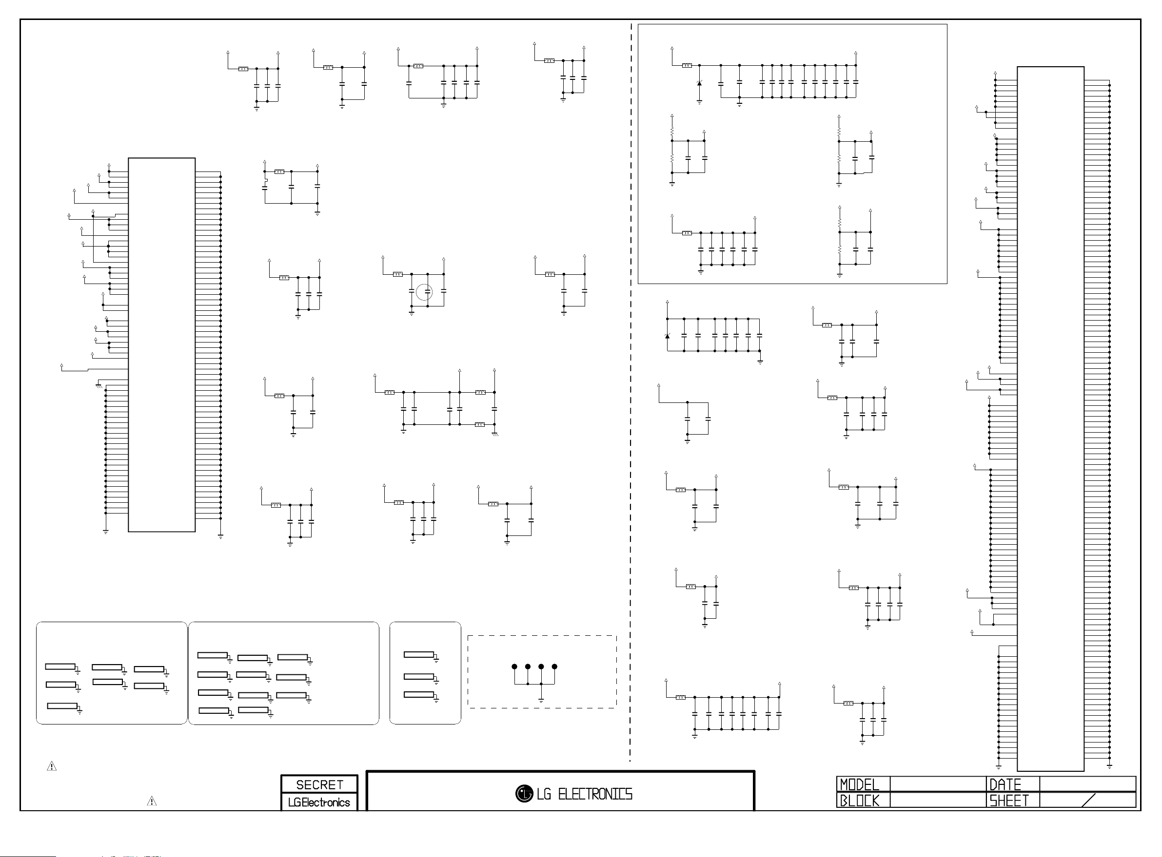
+1.0V_VDD
Copyright ⓒ 2013 LG Electronics. Inc. All right reserved.
Only for training and service purposes
LGE Internal Use Only
Max 360mA
AVDD10_DEMOD
L304
BLM18PG121SN1D
10uFC312
C318 0.1uF
C321 0.1uF
+1.0V_VDD
L302
BLM18PG121SN1D
LG1152A
IC101
VDD33
VDD33_CVBS
VDD33_HDMI
VDD33_XTAL
VDD25_VSB
VDD25_CVBS
VDD25_REF
VDD25_COMP
VDD25_AUD
VDD25_LVTX
VDD18_A
AVDD10_DEMOD
AVDD10_VSB
AVDD10_LVTX
VDDC_XTAL
+2.5V_NORMAL
For HDCP OTP
Will be change to LOW for MP
For HeatSinK SMD Top
3.0*4.0*4.0H
MDS62110218
MDS62110218
M300
M303
M304
MDS62110218
AVSS25_REF
M301
MDS62110218
M302
MDS62110218
P1
P2
P14
R14
F18
H16
M16
L15
R13
R12
V13
P10
R10
P9
R9
V7
J16
P6
P7
V6
B18
G12
G13
N1
N2
G6
G7
R15
K15
D17
D18
N7
L16
G4
N10
K16
D16
G5
G8
G9
G10
G11
G14
G15
H4
H5
H6
H7
H8
H9
H10
H11
H12
H13
H14
H15
J4
J5
J6
J7
VDD33_1
VDD33_2
AVDD33_CVBS_1
AVDD33_CVBS_2
AVDD33_HDMI_1
AVDD33_HDMI_2
VDD33_XTAL
VDD25_VSB
VDD25_CVBS_2
VDD25_CVBS_1
VDD25_CVBS_3
AVDD25_REF
VDD25_COMP_3
VDD25_COMP_1
VDD25_COMP_2
VDD25_COMP_4
VDD25_AAD
VDD25_AUD_1
VDD25_AUD_2
VDD25_AUD_3
VDD25_LVTX_1
VDD25_LVTX_2
VDD25_LVTX_3
VDD18_1
VDD18_2
VDDC10_1
VDDC10_2
AVDD10_CVBS
AVDD10_VSB
AVDD10_LVTX_1
AVDD10_LVTX_2
AVDD10_LLPLL
VDDC_XTAL
VQPS
AVSS25_REF
GND_XTAL
GND_1
GND_2
GND_3
GND_4
GND_5
GND_6
GND_7
GND_8
GND_9
GND_10
GND_11
GND_12
GND_13
GND_14
GND_15
GND_16
GND_17
GND_18
GND_19
GND_20
GND_21
GND_22
GND_23
GND_24
M305
MDS62110218
M306
MDS62110218
J8
GND_25
J9
GND_26
J10
GND_27
J11
GND_28
J12
GND_29
J13
GND_30
J14
GND_31
J15
GND_32
K4
GND_33
K5
GND_34
K6
GND_35
K7
GND_36
K8
GND_37
K9
GND_38
K10
GND_39
K11
GND_40
K12
GND_41
K13
GND_42
K14
GND_43
L4
GND_44
L5
GND_45
L6
GND_46
L7
GND_47
L8
GND_48
L9
GND_49
L10
GND_50
L11
GND_51
L12
GND_52
L13
GND_53
L14
GND_54
M4
GND_55
M5
GND_56
M6
GND_57
M7
GND_58
M8
GND_59
M9
GND_60
M10
GND_61
M11
GND_62
M12
GND_63
M13
GND_64
M14
GND_65
M15
GND_66
M17
GND_67
N4
GND_68
N5
GND_69
N6
GND_70
N8
GND_71
N9
GND_72
N11
GND_73
N12
GND_74
N13
GND_75
N14
GND_76
N15
GND_77
N16
GND_78
P3
GND_79
P4
GND_80
P5
GND_81
P13
GND_82
P15
GND_83
P16
GND_84
R3
GND_85
R16
GND_86
R17
GND_87
R18
GND_88
T13
GND_89
U13
GND_90
SMD Bottom
8.0*6.0*7.5H 8.0*6.0*7.5H
M315
MDS62110215
M312
MDS62110215
M313
MDS62110215
M314
MDS62110215
THE SYMBOL MARK OF THIS SCHEMETIC DIAGRAM INCORPORATES
SPECIAL FEATURES IMPORTANT FOR PROTECTION FROM X-RADIATION.
FILRE AND ELECTRICAL SHOCK HAZARDS, WHEN SERVICING IF IS
ESSENTIAL THAT ONLY MANUFATURES SPECFIED PARTS BE USED FOR
THE CRITICAL COMPONENTS IN THE SYMBOL MARK OF THE SCHEMETIC.
11/05/31
LG1152AN-B2
+1.8V_NORMAL
L326
BLM18PG121SN1D
10uFC421
+2.5V_NORMAL
L324
BLM18PG121SN1D
On Package Decap : 0.1uF *1ea
+2.5V_NORMAL
L322
BLM18PG121SN1D
On Package Decap : 0.1uF *1ea
+3.3V_NORMAL
L319
BLM18PG121SN1D
On Package Decap : 0.1uF *1ea
M318
MDS62110215
M317
MDS62110215
OPT
M310
MDS62110215
M311
MDS62110215
MDS62110215
MDS62110214
MDS62110214
10uFC422
Max 100mA
10uFC414
Max 50mA
10uFC401
Max 35mA
VDD33_CVBS
10uFC398
M308
M309
M322
VDD18_A
VDD25_CVBS
C417 0.1uF
VDD25_AUD
C403 0.1uF
C408 0.1uF
C423 0.1uF
C419 0.1uF
C409 0.1uF
10uFC305
Max 1mA
VDDC_XTAL
C313 0.1uF
+2.5V_NORMAL
+1.0V_VDD
10uFC359
L313
BLM18PG121SN1D
On Package Decap : 0.1uF *1ea
+2.5V_NORMAL
L315
BLM18PG121SN1D
10uFC379
On Package Decap : 0.1uF *1ea
+3.3V_NORMAL
L323
BLM18PG121SN1D
On Package Decap : 0.1uF *1ea
SMD Top
MDS62110217
MDS62110217
MDS62110217
L308
BLM18PG121SN1D
Max 250mA
VDD25_LVTX
10uFC375
C385 0.1uF
C386 0.1uF
Max 256mA
VDD33_HDMI
10uFC413
OPT
C405 0.1uF
M319
M316
M320
10uFC366
C390 0.1uF
Max 250mA
C416 0.1uF
C368 0.1uF
VDD25_COMP
C393 0.1uF
C407 0.1uF
Max 12mA
AVDD10_VSB
10uFC369
C370 0.1uF
Max 10mA
VDD25_REF
L321
BLM15BD121SN1
L320
C400 0.1uF
BLM15BD121SN1
AVSS25_REF
+3.3V_NORMAL
L309
BLM18PG121SN1D
GND JIG POINT
+1.0V_VDD
Max 35mA
AVDD10_LVTX
L305
BLM18PG121SN1D
10uFC332
C333 0.1uF
On Package Decap : 0.1uF *1ea
Max 28mA
L325
BLM18PG121SN1D
10uFC415
VDD25_VSB
+2.5V_NORMAL
On Package Decap : 0.1uF *1ea
Max 1mA
VDD33_XTAL
10uFC371
C381 0.1uF
JP302
JP301
JP300
JP303
C338 0.1uF
C418 0.1uF
+1.5V_Bypass Cap
+1.5V_DDR
L300
BLM18PG121SN1D
5V
ZD301
ESD_LG1152
VCC1.5V_MAIN
Max 40mA
VREF_M0
R300
1K 1%
0.1uF
R301
1K 1%
On Package Decap : 0.1uF *1ea
+1.5V_DDR
BLM18PG121SN1D
On Package Decap : 0.1uF *2ea
+0.9V_VDD
10uFC301
5V
ZD300
ESD_LG1152
On Package Decap : 0.1uF *6ea
+0.9V_VDD
On Package Decap : 0.1uF *1ea
+1.8V_NORMAL
L312
BLM18PG121SN1D
On Package Decap:0.1uF *1ea
+1.8V_NORMAL
On Package Decap:0.1uF *1ea
+3.3V_NORMAL
L310
BLM18PG121SN1D
On Package Decap : 0.1uF *1ea
C308
C300
L301
10uFC303
10uFC307
Max 20mA
10uFC347
Max 120mA
VDD18_LVTX
10uFC374
Max 93mA
VDD18_LVRX
L318
BLM18PG121SN1D
10uFC397
10uFC372
1000pF
C306 0.1uF
C314 0.1uF
C353 0.1uF
C382 0.1uF
C404 0.1uF
C377 0.1uF
10uFC326
C316 0.1uF
C310 0.1uF
Max 5900mA
C322 0.1uF
C319 0.1uF
C388 0.1uF
C383 0.1uF
(18)
10uFC302
C317 0.1uF
C311 0.1uF
C323 0.1uF
C320 0.1uF
On Package Decap : 0.1uF *3ea
Max 340mA
VCC1.5V_DE
C336 0.1uF
C340 0.1uF
C327 0.1uF
C325 0.1uF
VDD33
C392 0.1uF
C394 0.1uF
C399 0.1uF
C391 0.1uF
Max 680mA
VCC1.5V_MAIN
C329 0.1uF
C334 0.1uF
C337 0.1uF
VCC1.5V_MAIN
C342 0.1uF
R302
R303
C343 0.1uF
1K 1%
1K 1%
C346 0.1uF
Max 40mA
0.1uF
C350
VREF_M1
C362
On Package Decap : 0.1uF *1ea
Max 40mA
VCC1.5V_DE
R304
R305
VREF_M2
1K 1%
0.1uF
1K 1%
C363
C351
On Package Decap : 0.1uF *1ea
10uFC309
10uFC341
Max 6mA
C315 0.1uF
Max 1320mA
C345 0.1uF
MAIN_XTAL
C324 0.1uF
AVDD10_OSPREY
C348 0.33uF
+0.9V_VDD
+1.0V_VDD
L303
BLM18PG121SN1D
L306
BLM18PG121SN1D
On Package Decap : 0.1uF *3ea
+1.8V_NORMAL
L316
BLM18PG121SN1D
10uFC395
On Package Decap:0.1uF *1ea
+1.8V_NORMAL
+3.3V_NORMAL
L314
BLM18PG121SN1D
10uFC378
Max 48.8mA
L317
BLM18PG121SN1D
10uFC396
VDD18_MAIN_XTAL
VDD33_USB
C402 0.1uF
1000pF
1000pF
C349 0.33uF
Max 49mA
VDD18
C410 0.1uF
Max 31mA
C384 0.1uF
C389 0.1uF
C406 0.1uF
C411 0.1uF
C304 0.1uF
For secure BOOT OTP
Will be change to LOW for MP
LG1152
MAIN POWER
VDD33_USB
VDD18_LVTX
VDD18_LVRX
VDD18_MAIN_XTAL
VCC1.5V_DE
VCC1.5V_MAIN
VREF_M1
VREF_M0
AVDD10_OSPREY
+0.9V_VDD
+0.9V_VDD
MAIN_XTAL
VDD18
LG1152D
VDD33
U8
U9
U10
V8
V9
V10
J21
K21
AA10
AA11
VDD18
W18
W19
Y18
Y19
AG28
AH27
AA7
AA8
AA9
AG1
AA12
AA13
AB12
J28
B28
G22
F9
G8
G9
G10
G11
H8
H9
H10
H11
F22
G13
G14
G16
G17
G18
G19
G20
G21
H13
H14
H16
H17
H18
H19
H20
H21
VREF_M2
L4
F13
G12
F14
G15
L20
M20
M21
M27
M28
N20
N21
P20
P21
R20
R21
K8
K9
K10
K11
L8
L9
L10
L11
M8
M9
M10
M11
N8
N9
N10
N11
P8
P9
P10
P11
R8
R9
R10
R11
Y7
Y8
AF1
F28
H22
AA19
G23
G7
H7
H12
H15
J7
J8
J9
J10
J11
J12
J13
J14
J15
J16
J17
J18
J19
J20
K7
K12
IC100
LG1152D-B1
VDD33_1
VDD33_2
VDD33_3
VDD33_4
VDD33_5
VDD33_6
AVDD33_USB_1
AVDD33_USB_2
AVDD33_BT_USB_1
AVDD33_BT_USB_2
VDD18_1
VDD18_2
VDD18_3
VDD18_4
VDD18_5
VDD18_6
VDD18_LTX_1
VDD18_LTX_2
VDD18_LTX_3
VDD18_LTX_4
VDD18_LVRX_1
VDD18_LVRX_2
VDD18_LVRX_3
VDD18_DISPPLL
VDD18_DR3PLL
VDD18_MAIN_XTAL
VDD15_M2_1
VDD15_M2_2
VDD15_M2_3
VDD15_M2_4
VDD15_M2_5
VDD15_M2_6
VDD15_M2_7
VDD15_M2_8
VDD15_M2_9
VDD15_M0_1
VDD15_M0_2
VDD15_M0_3
VDD15_M0_4
VDD15_M0_5
VDD15_M0_6
VDD15_M0_7
VDD15_M0_8
VDD15_M0_9
VDD15_M0_10
VDD15_M0_11
VDD15_M0_12
VDD15_M0_13
VDD15_M0_14
VDD15_M0_15
VDD15_M0_16
VDD15_M0_17
VREF_M2_0
VREF_M1_0
VREF_M1_1
VREF_M0_0
VREF_M0_1
VDDC10_OSPREY_1
VDDC10_OSPREY_2
VDDC10_OSPREY_3
VDDC10_OSPREY_4
VDDC10_OSPREY_5
VDDC10_OSPREY_6
VDDC10_OSPREY_7
VDDC10_OSPREY_8
VDDC10_OSPREY_9
VDDC10_OSPREY_10
VDDC10_OSPREY_11
VDDC09_1
VDDC09_2
VDDC09_3
VDDC09_4
VDDC09_5
VDDC09_6
VDDC09_7
VDDC09_8
VDDC09_9
VDDC09_10
VDDC09_11
VDDC09_12
VDDC09_13
VDDC09_14
VDDC09_15
VDDC09_16
VDDC09_17
VDDC09_18
VDDC09_19
VDDC09_20
VDDC09_21
VDDC09_22
VDDC09_23
VDDC09_24
VDD09_LTX_1
VDD09_LTX_2
VDD09_LTX_3
AVDD09_DR3PLL
VDDC_MAIN_XTAL
SP_VQPS
GND_MAIN_XTAL
GND_1
GND_2
GND_3
GND_4
GND_5
GND_6
GND_7
GND_8
GND_9
GND_10
GND_11
GND_12
GND_13
GND_14
GND_15
GND_16
GND_17
GND_18
GND_19
GND_20
3
GND_21
GND_22
GND_23
GND_24
GND_25
GND_26
GND_27
GND_28
GND_29
GND_30
GND_31
GND_32
GND_33
GND_34
GND_35
GND_36
GND_37
GND_38
GND_39
GND_40
GND_41
GND_42
GND_43
GND_44
GND_45
GND_46
GND_47
GND_48
GND_49
GND_50
GND_51
GND_52
GND_53
GND_54
GND_55
GND_56
GND_57
GND_58
GND_59
GND_60
GND_61
GND_62
GND_63
GND_64
GND_65
GND_66
GND_67
GND_68
GND_69
GND_70
GND_71
GND_72
GND_73
GND_74
GND_75
GND_76
GND_77
GND_78
GND_79
GND_80
GND_81
GND_82
GND_83
GND_84
GND_85
GND_86
GND_87
GND_88
GND_89
GND_90
GND_91
GND_92
GND_93
GND_94
GND_95
GND_96
GND_97
GND_98
GND_99
GND_100
GND_101
GND_102
GND_103
GND_104
GND_105
GND_106
GND_107
GND_108
GND_109
GND_110
GND_111
GND_112
GND_113
GND_114
GND_115
GND_116
GND_117
GND_118
GND_119
GND_120
GND_121
GND_122
GND_123
GND_124
GND_125
GND_126
GND_127
GND_128
GND_129
GND_130
GND_131
GND_132
GND_133
GND_134
GND_135
GND_136
GND_137
GND_138
GND_139
GND_140
GND_141
GND_142
GND_143
GND_144
GND_145
GND_146
GND_147
GND_148
K13
K14
K15
K16
K17
K18
K19
K20
L7
L12
L13
L14
L15
L16
L17
L18
L19
L21
M7
M12
M13
M14
M15
M16
M17
M18
M19
N7
N12
N13
N14
N15
N16
N17
N18
N19
P7
P12
P13
P14
P15
P16
P17
P18
P19
R7
R12
R13
R14
R15
R16
R17
R18
R19
T7
T8
T9
T10
T11
T12
T13
T14
T15
T16
T17
T18
T19
T20
T21
U7
U11
U12
U13
U14
U15
U16
U17
U18
U19
U20
U21
V11
V12
V13
V14
V15
V16
V17
V18
V19
V20
V21
W7
W8
W9
W10
W11
W12
W13
W14
W15
W16
W17
W20
W21
Y9
Y10
Y11
Y12
Y13
Y14
Y15
Y16
Y17
Y20
Y21
AA14
AA15
AA16
AA17
AA18
AA20
AA21
AB7
AB10
AB11
AB13
AB22
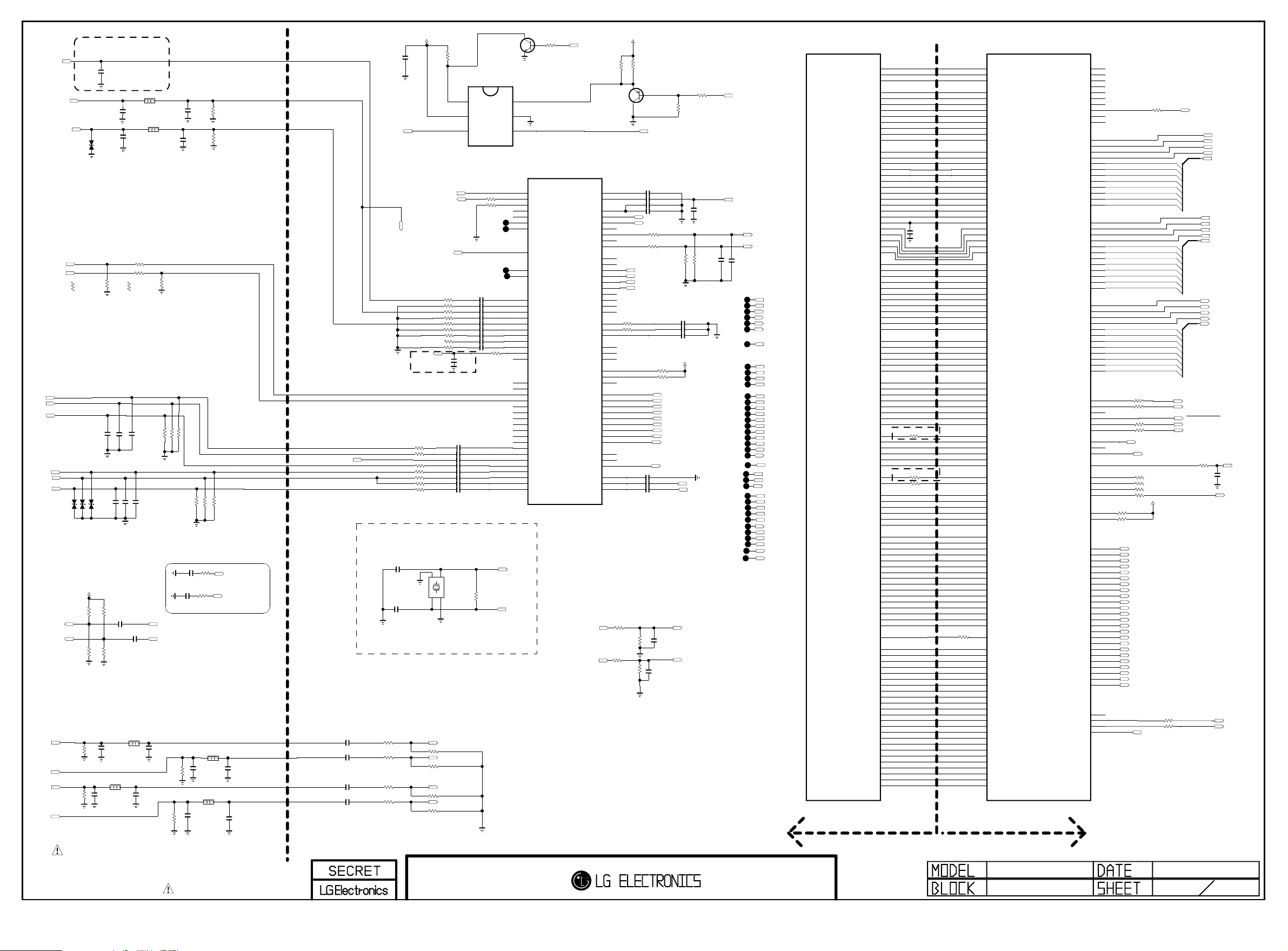
Place these close to tuner
Copyright ⓒ 2013 LG Electronics. Inc. All right reserved.
Only for training and service purposes
LGE Internal Use Only
TU_CVBS
680pF
C506
OPT
L503
SC_CVBS_IN
AV1_CVBS_IN
SC_B
SC_G
SC_R
COMP1_Pb
COMP1_Y
COMP1_Pr
SC_FB
SC_ID
D503
5.5V
D504
5.5V
NON SCART
R525-*1
0
D506
D505
5.5V
5.5V
C528
OPT
10pF
EU
R525
75
C580
C546
10pF
R522
OPT
10pF
C579
C508
150pF
50V
EU
50V
150pF
C511
R521 100
10K
NON SCART
R524-*1
0
OPT
10pF
C524
10pF
10pF
C578
EU
EU
L504
1uH
C509
R614
150pF
75
EU
C514
150pF
50V
75
1%
R606
75
1%
R605
75
1%
R604
1%
R615
75
1%
DTV/MNT_V_OUT
SC_SOG_IN
SC_SOG_IN
1uH
EU
R524
2.7K
75
75
75
R595
R600
R594
Main clock for LG1152A
SCART_Lout
SCART_Rout
SC_L_IN
SC_R_IN
AV1_L_IN
AV1_R_IN
EU
R602
470K
R603
470K
+12V
100K
100K
R552
R554
C574
560pF
50V
OPT
EU
EU
100K
100K
C572
330pF
50V
OPT
L508
R538
2.2uF
10V
R549
Near Place Scart AMP
EU
EU
C525
EU
2.2uF
L507
EU
SCART_Lout_SOC
EU
SCART_Rout_SOC
C522
10V
C576
330pF
50V
EU
C577
100pF
50V
R609
470K
Place JACK Side
470K
EU
R608
C6006
EU
1uF 25V
C6001
EU
EU
SCART_AMP_R_FB
10K
1uF25V
R60 06
EU
SCART_AMP_L_FB
10K
R6005
C502
2.2uF
C503
C504
C505
EU
EU
2.2uF
2.2uF
2.2uF
C586
560pF
50V
OPT
C582
330pF
50V
OPT
L511
EU
L510
EU
C588
330pF
50V
C589
100pF
50V
Place SOC Side
C513
C512
R510
EU
R511
EU
R512 22K
R513 22K
8pF
8pF
22K
22K
THE SYMBOL MARK OF THIS SCHEMETIC DIAGRAM INCORPORATES
SPECIAL FEATURES IMPORTANT FOR PROTECTION FROM X-RADIATION.
FILRE AND ELECTRICAL SHOCK HAZARDS, WHEN SERVICING IF IS
ESSENTIAL THAT ONLY MANUFATURES SPECFIED PARTS BE USED FOR
THE CRITICAL COMPONENTS IN THE SYMBOL MARK OF THE SCHEMETIC.
+5V_NORMAL
EU
C510
0.1uF
16V
SOC_RESET
R571 33
R572 33
R573 100
R574 100
R551 33
R575 33
DTV/MNT_VOUT
Close to LG1152A
R568 33
R569 33
R570 33
R564 150
R565 150
R566 0
R567 150
EU
R516 75K
EU
R517 100K
R518 75K
R519 100K
10K
SELECT
XIN_SUB
XO_SUB
R559 68
R557 33
R558 68
C542 0.047uF
C543 0.047uF
C544 1000pF
C545 0.047uF
C538 0.047uF
C539 0.047uF
C540 1000pF
C541 0.047uF
X-TAL_1
GND_1
1
2
24MHz
4
3
GND_2
X-TAL_2
AUAD_L_CH4_IN
AUAD_R_CH4_IN
AUAD_L_CH3_IN
AUAD_R_CH3_IN
EU
R527
X500
Q506
MMBT3904(NXP)
IC500
NLASB3157DFT2G
EU
R560
R561
0.047uF
0.047uF
0.047uF
0.047uF
0.047uF
0.047uF
0.047uF
0.047uF
0.047uF
R563 0
EU
1M
1
2
3
330
33
XIN_SUB
XO_SUB
6
VCC
5
A
4
Selece = High ==> A = B1
Selece = Low ==> A = B0
C549
C550
C551
C552
C553
C554
C555
C556
C557
C515
100pF
50V
EU
R535
C
E
B1
GND
B0
L17
L18
P17
K17
K18
M2
M1
R4
N3
M3
U14
T14
V15
U15
T15
U16
V14
T16
V16
V17
U17
P8
R8
P11
R11
U8
V8
V10
T8
V9
T11
U9
T9
U10
T10
V11
U11
V12
U12
T12
EU
XIN_SUB
XO_SUB
VSB_AUX_XIN
XTLIN_AAD
XTLOUT_AAD
OPM1
OPM0
PORES_N
L9A_SCL
L9A_SDA
CVBS_IN1
CVBS_IN2
CVBS_IN3
CVBS_VCM
CVBS_IN4
CVBS_IN5
CVBS_IN6
CB_IN
CB_VCM
BUF_OUT1
BUF_OUT2
HSYNC
VSYNC
SC1_FB
SC1_SID
BINCOM_IN
B_IN
GINCOM_IN
G_IN
SOG_IN
RINCOM_IN
R_IN
PB1_IN
Y1_IN
SOY1_IN
PR1_IN
PB2_IN
Y2_IN
SOY2_IN
PR2_IN
B
EU
R507
10K
IC101
LG1152AN-B2
AAD_ADC_SIFM
AAD_ADC_SIF
AUDA_BGR_OUT
AUD_SCART0_OUTLN
AUD_SCART0_OUTLP
AUD_SCART0_OUTRN
AUD_SCART0_OUTRP
AUAD_L_CH5_IN
AUAD_R_CH5_IN
AUAD_L_CH4_IN
AUAD_R_CH4_IN
AUAD_L_CH3_IN
AUAD_R_CH3_IN
AUAD_L_CH2_IN
AUAD_R_CH2_IN
AUAD_L_CH1_IN
AUAD_R_CH1_IN
AUAD_VR_OUT
PHY0_RXCN_0
PHY0_RXCP_0
PHY0_RX0N_0
PHY0_RX0P_0
PHY0_RX1N_0
PHY0_RX1P_0
PHY0_RX2N_0
PHY0_RX2P_0
PHY0_ARC_OUT_0
ADC_I_INCOM
AUDA_OUTR
DTV_ATV_SELECT
AUDA_OUTL
AUDA_OUTR
AUAD_REFN
AUAD_REFP
AUMI_BIAS
AUMI_IN
AUMI_COM
DDCD0_DA
DDCD0_CK
HPD0
ANTCON
RFAGC
IFAGC
ADC_I_INP
ADC_I_INN
AUDA_OUTL
+5V_NORMAL
R592
220
EU
EU
Q504
MMBT3906(NXP)
N17
N18
U1
R1
R2
T1
V2
U2
T2
U3
V3
V4
T3
U5
T5
U6
T6
U7
T7
T4
10K
U4
V5
R7
R5
R6
E18
E17
E16
J18
J17
H17
H18
G17
G18
G16
F16
F17
P12
M18
P18
T17
U18
T18
R624
100
R625
100
R593
220
EU
E
B
C
DTV/MNT_VOUT
C533 0.1uF
C534 0.1uF
10uFC535
C536 2.2uF
AUDA_OUTL
AUDA_OUTR
EU
EU
AUAD_L_CH4_IN
AUAD_R_CH4_IN
AUAD_L_CH3_IN
AUAD_R_CH3_IN
R534
R52010K
R577 4.7K
R578 4.7K
0.1uF
C115
0.1uF
C116
0.1uF
C117
H/NIM&CHB
H/NIM&CHB
R626
22K
C604
0.01uF
R627
22K
R599
75
R501100
R502100
+3.3V_NORMAL
HDMI_CLKHDMI_CLK+
HDMI_RX0HDMI_RX0+
HDMI_RX1HDMI_RX1+
HDMI_RX2HDMI_RX2+
SPDIF_OUT_ARC
IF_AGC
C603
0.01uF
EU
OPT
C558
1000pF
OPT
22K
EU
EU
R531
R532 22K
C5372.2uF
C5472.2uF
C5482.2uF
IF_N
IF_P
HP_LOUT_MAIN
HP_ROUT_MAIN
IC101
LG1152AN-B2
L1
INTR_GBB
L2
INTR_HDMI1
BB_TP_VAL
BB_TP_SOP
BB_TP_ERR
BB_TP_CLK
BB_SDA_I
BB_SDA_O
BB_SCL
L9DA_SCL
L9DA_SDA_I
L9DA_SDA_O
CHB_DN
CHB_UP
CHB_START
CHB_DATA0
CHB_DATA1
CHB_DATA2
CHB_DATA3
CHB_DATA4
CLK_F54M
CVBS_GC2
CVBS_GC1
CVBS_GC0
CVBS_UP
CVBS_DN
FS00CLK
AUDCLK_OUT
DAC_DATA0
DAC_DATA1
DAC_DATA2
DAC_DATA3
DAC_DATA4
DAC_START
AAD_GC0
AAD_GC1
AAD_GC2
AAD_GC3
AAD_GC4
AAD_DATAEN
AAD_DATA0
AAD_DATA1
AAD_DATA2
AAD_DATA3
AAD_DATA4
AAD_DATA5
AAD_DATA6
AAD_DATA7
AAD_DATA8
AAD_DATA9
HSR_AM0
HSR_AP0
HSR_BM0
HSR_BP0
HSR_CM0
HSR_CP0
HSR_CLKM0
HSR_CLKP0
HSR_DM0
HSR_DP0
HSR_EM0
HSR_EP0
HSR_AM1
HSR_AP1
HSR_BM1
HSR_BP1
HSR_CM1
HSR_CP1
HSR_CLKM1
HSR_CLKP1
HSR_DM1
HSR_DP1
HSR_EM1
HSR_EP1
L3
K1
K2
J2
J3
K3
H1
H2
H3
J1
G1
G2
G3
B1
C1
A4
B4
C4
A2
D1
D2
E2
E1
F1
F2
B2
A3
C2
B3
C3
D3
E3
F3
D4
E4
F4
D5
E5
F5
D6
A5
B5
C5
A6
B6
C6
E6
F6
D7
B7
C7
A8
B8
C8
Close to LG1152A
A7
R581 33
D8
F7
E7
E8
F8
Close to LG1152A
A9
R582 33
B9
R583 33
C9
D9
E9
F9
C10
D10
E10
F10
D11
E11
F11
D12
E12
F12
D13
E13
F13
D14
E14
F14
D15
E15
F15
B10
A10
A11
B11
C12
C11
B12
A12
A13
B13
C14
C13
B14
A14
A15
B15
C16
C15
B16
A16
A17
B17
C18
C17
C529
220pF
OPT
50V
R576100
ATV_OUT
TUNER_SIF
SCART_Lout_SOC
SCART_Rout_SOC
EU
EU
C520 0.01uF
C521 0.01uF
TPI_SOP
TPI_CLK
TPO_ERR
TPO_VAL
TPO_SOP
TPO_CLK
JDVR_SCLK
TU_CVBS
SCART_Lout
SCART_Rout
SC_R
SC_CVBS_IN
SC_B
SC_G
SC_FB
SC_ID
ATV_OUT
SC_L_IN
SC_R_IN
TUNER_SIF
TUNER_SIF
DTV/MNT_V_OUT
JDVR_SCLK
IF_N
IF_P
IF_AGC
FE_TS_CLK
FE_TS_SYNC
FE_TS_VAL
TPI_DVB_ERR
FE_TS_DATA[0-7]
TPO_DATA[0-7]
TPI_DATA[0-7]
TPI_ERR
TPI_VAL
OPTIC_GPIO1
OPTIC_BACK_CHANNEL
INTR_AFE3CH
AUD_HMR00ARC
AUD_HMR0AMUTE
AUD_HMR0ALRCK
AUD_HMR0ABCK
AUD_HMR0ASD4
AUD_HMR0ASD3
AUD_HMR0ASD2
AUD_HMR0ASD1
AUD_HMR0ASD0
AUD_DAC1_LRCH
AUD_DAC1_SCK
AUD_DAC1_LRCK
AUD_FS25CLK
AUD_FS24CLK
AUD_FS23CLK
AUD_FS21CLK
AUD_FS20CLK
AUDCLK_OUT_SUB
AUD_DAC0_LRCK
AUD_DAC0_LRCH
AUD_DAC0_SCK
AUD_ADC_LRCH
AUD_ADC_SCK
AUD_ADC_LRCK
AUD_MIC_LRCH
AUD_MIC_SCK
AUD_MIC_LRCK
BB_TP_DATA0
BB_TP_DATA1
BB_TP_DATA2
BB_TP_DATA3
BB_TP_DATA4
BB_TP_DATA5
BB_TP_DATA6
BB_TP_DATA7
DCO_OUT_CLK
R9112
33
AH2
INTR_GBB
AG2
INTR_HDMI1
AF2
INTR_AFE3CH
AH3
AUD_HMR0ARC
AG3
AUD_HMR0AMUTE
AG4
AUD_HMR0ALRCK
AF4
AUD_HMR0ABCK
AF3
AUD_HMR0ASD4
AH5
AUD_HMR0ASD3
AG5
AUD_HMR0ASD2
AF5
AUD_HMR0ASD1
AH4
AUD_HMR0ASD0
AH6
AUD_DAC1_LRCH
AG6
AUD_DAC1_SCK
AF6
AUD_DAC1_LRCK
AH7
AUD_FS25CLK
AG7
AUD_FS24CLK
AH10
AUD_FS23CLK
AG10
AUD_FS21CLK
AF10
AUD_FS20CLK
AH8
AUDCLK_OUT_SUB
AF7
AUD_DAC0_LRCK
AE8
AUD_DAC0_LRCH
AD8
AUD_DAC0_SCK
AE7
AUD_ADC_LRCH
AD7
AUD_ADC_SCK
AC8
AUD_ADC_LRCK
AG8
AUD_MIC_LRCH
AH9
AUD_MIC_SCK
AF8
AUD_MIC_LRCK
AG9
BB_TPI_DATA0
AF9
BB_TPI_DATA1
AE9
BB_TPI_DATA2
AD9
BB_TPI_DATA3
AC9
BB_TPI_DATA4
AE10
BB_TPI_DATA5
AD10
BB_TPI_DATA6
AC10
BB_TPI_DATA7
AE11
BB_TPI_VAL
AD11
BB_TPI_SOP
AC11
BB_TPI_ERR
AE12
BB_TPI_CLK
AH11
BB_SDA_I
AG11
BB_SDA_O
AF11
BB_SCL
AH12
HS_SCL
AG12
HS_SDA_I
AF12
HS_SDA_O
AD12
CHB_DN
AC12
CHB_UP
AE13
CHB_START
AG13
CHB_DATA0
AF13
CHB_DATA1
AH14
CHB_DATA2
AG14
CHB_DATA3
AF14
CHB_DATA4
AH13
CLK_54
AE14
CVBS_GC2
AC13
CVBS_GC1
AD13
CVBS_GC0
AD14
CVBS_UP
AC14
CVBS_DN
AH15
FS00CLK
AG15
AUDCLK_TO_DIGITAL
AF15
DAC_DATA0
AE15
DAC_DATA1
AD15
DAC_DATA2
AC15
DAC_DATA3
AF16
DAC_DATA4
AE16
DAC_START
AD16
AAD_GC0
AC16
AAD_GC1
AE17
AAD_GC2
AD17
AAD_GC3
AC17
AAD_GC4
AE18
AAD_DATAEN
AD18
AAD_DATA0
AC18
AAD_DATA1
AE19
AAD_DATA2
AD19
AAD_DATA3
AC19
AAD_DATA4
AE20
AAD_DATA5
AD20
AAD_DATA6
AC20
AAD_DATA7
AE21
AAD_DATA8
AD21
AAD_DATA9
AC21
AUPLL_CLK
AG16
HS_RX1_AM
AH16
HS_RX1_AP
AH17
HS_RX1_BM
AG17
HS_RX1_BP
AF18
HS_RX1_CM
AF17
HS_RX1_CP
AG18
HS_RX1_CLKM
AH18
HS_RX1_CLKP
AH19
HS_RX1_DM
AG19
HS_RX1_DP
AF20
HS_RX1_EM
AF19
HS_RX1_EP
AG20
HS_RX2_AM
AH20
HS_RX2_AP
AH21
HS_RX2_BM
AG21
HS_RX2_BP
AF22
HS_RX2_CM
AF21
HS_RX2_CP
AG22
HS_RX2_CLKM
AH22
HS_RX2_CLKP
AH23
HS_RX2_DM
AG23
HS_RX2_DP
AF24
HS_RX2_EM
AF23
HS_RX2_EP
IC100
LG1152D-B1
STPIO_SOP/GPIO43
STPIO_VAL/GPIO42
STPIO_ERR/GPIO41
STPIO_DATA/GPIO40
TPI_DVB_CLK/GPIO47
TPI_DVB_SOP/GPIO46
TPI_DVB_VAL/GPIO45
TPI_DVB_DATA0/GPIO44
PCMI3LRCK/GPIO81
AUD_SUBSCK/GPIO51
AUD_SUBLRCK/GPIO52
STPI_CLK
STPI_SOP
STPI_VAL
STPI_ERR
STPI_DATA
STPIO_CLK
TPI_DVB_ERR
TPI_DVB_DATA1
TPI_DVB_DATA2
TPI_DVB_DATA3
TPI_DVB_DATA4
TPI_DVB_DATA5
TPI_DVB_DATA6
TPI_DVB_DATA7
TPI_CLK
TPI_SOP
TPI_VAL
TPI_ERR
TPI_DATA0
TPI_DATA1
TPI_DATA2
TPI_DATA3
TPI_DATA4
TPI_DATA5
TPI_DATA6
TPI_DATA7
TPO_CLK
TPO_SOP
TPO_VAL
TPO_ERR
TPO_DATA0
TPO_DATA1
TPO_DATA2
TPO_DATA3
TPO_DATA4
TPO_DATA5
TPO_DATA6
TPO_DATA7
AUDCLK_OUT
DACLRCH
DACSLRCH/GPIO95
DACCLFCH/GPIO94
DACSCK
DACLRCK
PCMI3LRCH
PCMI3SCK/GPIO80
IEC958OUT
AUD_SUBMCK
AUD_SUBLRCH
BTSCSEL
DTS_EN
TXA0N
TXA0P
TXA1N
TXA1P
TXA2N
TXA2P
TXACLKN
TXACLKP
TXA3N
TXA3P
TXA4N
TXA4P
TXB0N
TXB0P
TXB1N
TXB1P
TXB2N
TXB2P
TXBCLKN
TXBCLKP
TXB3N
TXB3P
TXB4N
TXB4P
PWM0/GPIO55
PWM1/GPIO54
PWM2/GPIO53
PWM_IN
AE27
AE26
AD28
AD27
AD26
AC28
AC26
AB28
AC27
AB27
AF27
AE28
AG27
AF28
AG26
AF26
AF25
AH26
AH25
AG25
AH24
AG24
H24
J25
J24
H25
J27
J26
H28
H27
H26
G28
G27
G26
D24
E23
D25
D23
H23
G25
G24
F25
F24
F23
E25
E24
C1
C2
A3
A2
B2
B1
B3
C3
A4
AE2
R598 47
AD25
R619 47
AC25
R628 22
AD24
R629 47
AE25
AB18
AB19
DTS_EN: ENABLE(’1’) (for development)
BTSC_EN: ENABLE(’1’) (for development)
N1
N2
P2
P1
P3
R3
R1
R2
T2
T1
T3
U3
U1
U2
V2
V1
V3
W3
W1
W2
Y2
Y1
Y3
AA3
L6
L5
M4
M5
R59622
R59722
SOC_TXA0N
SOC_TXA0P
SOC_TXA1N
SOC_TXA1P
SOC_TXA2N
SOC_TXA2P
SOC_TXACLKN
SOC_TXACLKP
SOC_TXA3N
SOC_TXA3P
SOC_TXA4N
SOC_TXA4P
SOC_TXB0N
SOC_TXB0P
SOC_TXB1N
SOC_TXB1P
SOC_TXB2N
SOC_TXB2P
SOC_TXBCLKN
SOC_TXBCLKP
SOC_TXB3N
SOC_TXB3P
SOC_TXB4N
SOC_TXB4P
EDGE_LED
33
R556
FE_TS_DATA[0]
FE_TS_DATA[1]
FE_TS_DATA[2]
FE_TS_DATA[3]
FE_TS_DATA[4]
FE_TS_DATA[5]
FE_TS_DATA[6]
FE_TS_DATA[7]
TPI_DATA[0]
TPI_DATA[1]
TPI_DATA[2]
TPI_DATA[3]
TPI_DATA[4]
TPI_DATA[5]
TPI_DATA[6]
TPI_DATA[7]
TPO_DATA[0]
TPO_DATA[1]
TPO_DATA[2]
TPO_DATA[3]
TPO_DATA[4]
TPO_DATA[5]
TPO_DATA[6]
TPO_DATA[7]
R542100
100
R543
100
R544
100
R545
OPTIC_BACK_CHANNEL
OPTIC_GPIO1
OPT
OPT
OPT
+3.3V_NORMAL
R632
R633
BPL_IN
R630 100
100
100
USB_CTL2
FE_TS_CLK
FE_TS_SYNC
FE_TS_VAL
TPI_DVB_ERR
FE_TS_DATA[0-7]
TPI_CLK
TPI_SOP
TPI_VAL
TPI_ERR
TPI_DATA[0-7]
TPO_CLK
TPO_SOP
TPO_VAL
TPO_ERR
TPO_DATA[0-7]
AUD_MASTER_CLK
AUD_LRCH
FRC3_FLASH_WP
AUD_SCK
AUD_LRCK
C630
82pF
50V
AMP_RESET_N
PWM_DIM2
PWM_DIM
SPDIF_OUT
LG1152A LG1152D
LG1152 B0
MAIN AUDIO/VIDEO
3
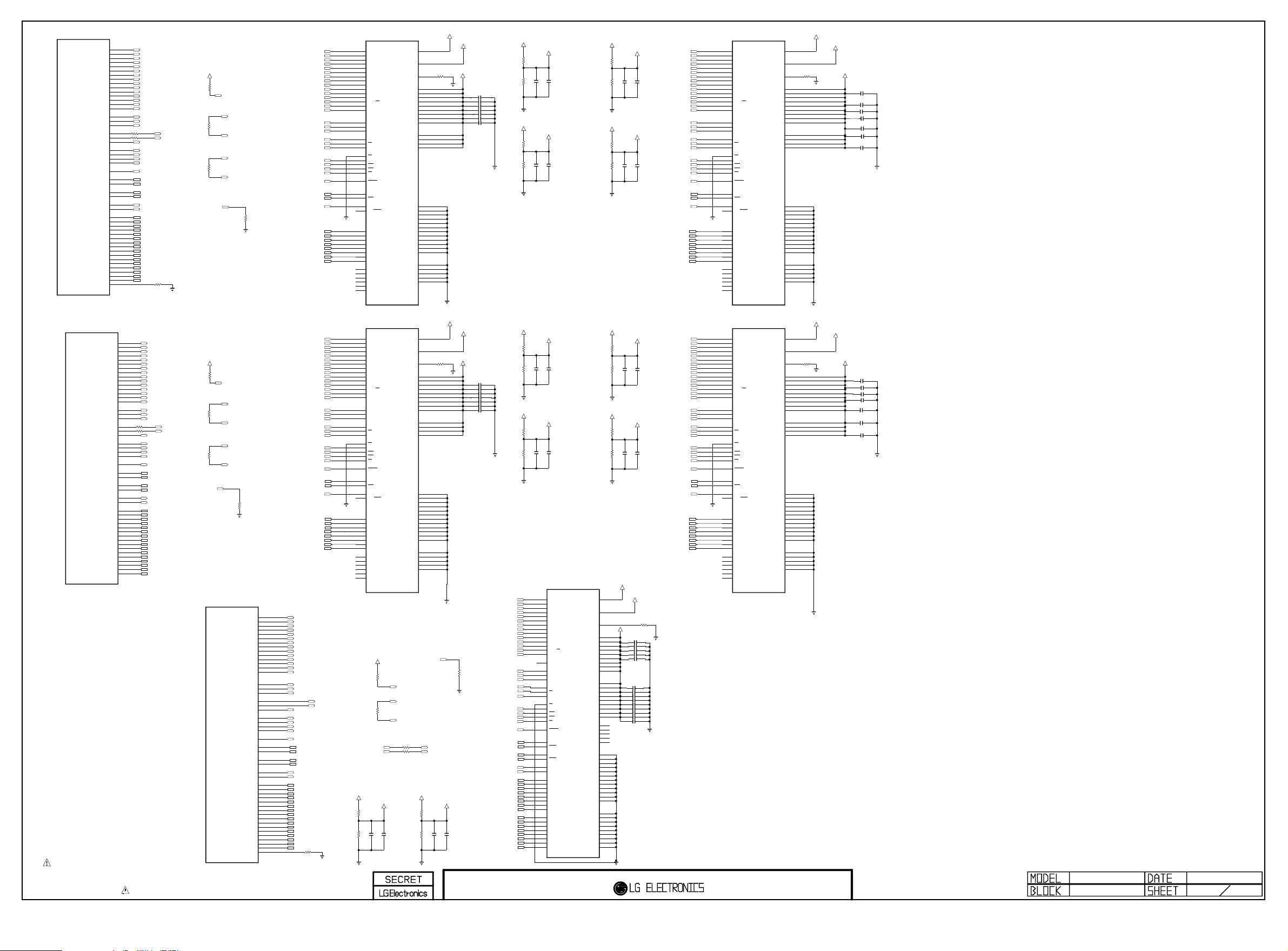
IC100
Copyright ⓒ 2013 LG Electronics. Inc. All right reserved.
Only for training and service purposes
LGE Internal Use Only
LG1152D-B1
M0_DDR_RESET_N
M0_DDR_DQSL_P
M0_DDR_DQSL_N
M0_DDR_DQSU_P
M0_DDR_DQSU_N
M0_DDR_ZQCAL
M0_DDR_A0
M0_DDR_A1
M0_DDR_A2
M0_DDR_A3
M0_DDR_A4
M0_DDR_A5
M0_DDR_A6
M0_DDR_A7
M0_DDR_A8
M0_DDR_A9
M0_DDR_A10
M0_DDR_A11
M0_DDR_A12
M0_DDR_A13
M0_DDR_A14
M0_DDR_BA0
M0_DDR_BA1
M0_DDR_BA2
M0_DDR_CLK
M0_DDR_CLKN
M0_DDR_CKE
M0_DDR_ODT
M0_DDR_RASN
M0_DDR_CASN
M0_DDR_WEN
M0_DDR_DML
M0_DDR_DMU
M0_DDR_DQ0
M0_DDR_DQ1
M0_DDR_DQ2
M0_DDR_DQ3
M0_DDR_DQ4
M0_DDR_DQ5
M0_DDR_DQ6
M0_DDR_DQ7
M0_DDR_DQ8
M0_DDR_DQ9
M0_DDR_DQ10
M0_DDR_DQ11
M0_DDR_DQ12
M0_DDR_DQ13
M0_DDR_DQ14
M0_DDR_DQ15
D18
E17
E18
E20
E16
D20
F16
F19
E15
D19
D14
E14
D17
F18
D16
F20
D15
F17
A17
A18
F15
F21
D22
E21
D21
E19
B20
A20
B16
C16
C19
C15
C20
B19
C21
B18
A21
C18
B21
A19
B17
C14
A16
B14
B15
A14
C17
A15
E22
R700 0
R701 0
SIGN50005
M0_DDR_A0
M0_DDR_A1
M0_DDR_A2
M0_DDR_A3
M0_DDR_A4
M0_DDR_A5
M0_DDR_A6
M0_DDR_A7
M0_DDR_A8
M0_DDR_A9
M0_DDR_A10
M0_DDR_A11
M0_DDR_A12
M0_DDR_A13
M0_DDR_A14
M0_DDR_BA0
M0_DDR_BA1
M0_DDR_BA2
M0_DDR_CKE
M0_DDR_ODT
M0_DDR_RASN
M0_DDR_CASN
M0_DDR_WEN
M0_DDR_RESET_N
M0_DDR_DQSL_P
M0_DDR_DQSL_N
M0_DDR_DQSU_P
M0_DDR_DQSU_N
M0_DDR_DML
M0_DDR_DMU
M0_DDR_DQ0
M0_DDR_DQ1
M0_DDR_DQ2
M0_DDR_DQ3
M0_DDR_DQ4
M0_DDR_DQ5
M0_DDR_DQ6
M0_DDR_DQ7
M0_DDR_DQ8
M0_DDR_DQ9
M0_DDR_DQ10
M0_DDR_DQ11
M0_DDR_DQ12
M0_DDR_DQ13
M0_DDR_DQ14
M0_DDR_DQ15
240
1%
M0_DDR_CLK
M0_DDR_CLKN
R704
VCC1.5V_MAIN
R709
10K
R705
200
R706
200
M0_DDR_CKE
M0_DDR_RESET_N
M0_DDR_CLK
M0_DDR_CLKN
M0_DDR_CLK
M0_DDR_CLKN
IC700
H5TQ2G83DFR-PBC
DDR3
K3
M0_DDR_A0
M0_DDR_A1
M0_DDR_A2
M0_DDR_A3
M0_DDR_A4
M0_DDR_A5
M0_DDR_A6
M0_DDR_A7
M0_DDR_A8
M0_DDR_A9
M0_DDR_A10
M0_DDR_A11
M0_DDR_A12
M0_DDR_A13
M0_DDR_A14
M0_DDR_BA0
M0_DDR_BA1
M0_DDR_BA2
M0_DDR_CLK
M0_DDR_CLKN
M0_DDR_CKE
M0_DDR_ODT
M0_DDR_RASN
M0_DDR_CASN
M0_DDR_WEN
M0_DDR_RESET_N
M0_DDR_DQSL_P
M0_DDR_DQSL_N
R742
10K
M0_DDR_DML
M0_DDR_DQ0
M0_DDR_DQ1
M0_DDR_DQ6
M0_DDR_DQ4
M0_DDR_DQ3
M0_DDR_DQ2
M0_DDR_DQ5
2Gbit
A0
L7
A1
L3
A2
K2
A3
L8
A4
L2
A5
M8
A6
M2
A7
N8
A8
M3
A9
H7
A10/AP
M7
A11
K7
A12/BC
N3
A13
N7
A14
J2
BA0
K8
BA1
J3
BA2
F7
CK
G7
CK
G9
CKE
H2
CS
G1
ODT
F3
RAS
G3
CAS
H3
WE
N2
RESET
C3
DQS
D3
DQS
B7
DM/TDQS
A7
NU/TDQS
B3
DQ0
C7
DQ1
C2
DQ2
C8
DQ3
E3
DQ4
E8
DQ5
D2
DQ6
E7
DQ7
A3
NC_1
F1
NC_2
F9
NC_3
H1
NC_4
H9
NC_5
J7
NC_6
VREFCA
VREFDQ
VDDQ_1
VDDQ_2
VDDQ_3
VDDQ_4
VSS_10
VSS_11
VSS_12
VSSQ_1
VSSQ_2
VSSQ_3
VSSQ_4
VSSQ_5
VDD_1
VDD_2
VDD_3
VDD_4
VDD_5
VDD_6
VDD_7
VDD_8
VDD_9
VSS_1
VSS_2
VSS_3
VSS_4
VSS_5
VSS_6
VSS_7
VSS_8
VSS_9
M0_DDR_VREFCA
M0_DDR_VREFDQ
J8
E1
VCC1.5V_MAIN
R720
H8
ZQ
240
1%
A2
A9
D7
G2
G8
K1
K9
M1
M9
B9
C1
E2
E9
A1
A8
B1
D8
F2
F8
J1
J9
L1
L9
N1
N9
B2
B8
C9
D1
D9
C706 0.1uF
C707
C708
C709
C710
C711
C712
0.1uF
0.1uF
0.1uF
0.1uF
0.1uF
0.1uF
VCC1.5V_MAIN
R722
R723
1K 1%
VCC1.5V_MAIN
R724
R725
1K 1%
1K 1%
C724
1K 1%
C725
M0_DDR_VREFCA
0.1uF
C728
M0_DDR_VREFDQ
0.1uF
C729
1000pF
1000pF
VCC1.5V_MAIN
R730
R731
1K 1%
VCC1.5V_MAIN
R732
R733
1K 1%
M0_1_DDR_VREFCA
1K 1%
C732
M0_1_DDR_VREFDQ
1K 1%
C733
0.1uF
0.1uF
M0_DDR_A0
M0_DDR_A1
M0_DDR_A2
M0_DDR_A3
M0_DDR_A4
M0_DDR_A5
M0_DDR_A6
M0_DDR_A7
1000pF
M0_DDR_A8
1000pF
M0_DDR_A9
M0_DDR_A10
M0_DDR_A11
M0_DDR_A12
M0_DDR_A13
M0_DDR_A14
M0_DDR_BA0
M0_DDR_BA1
M0_DDR_BA2
M0_DDR_CLK
M0_DDR_CLKN
M0_DDR_CKE
M0_DDR_ODT
M0_DDR_RASN
M0_DDR_CASN
M0_DDR_WEN
M0_DDR_RESET_N
M0_DDR_DQSU_P
M0_DDR_DQSU_N
M0_DDR_DMU
M0_DDR_DQ10
M0_DDR_DQ13
M0_DDR_DQ14
M0_DDR_DQ11M0_DDR_DQ7
M0_DDR_DQ15
M0_DDR_DQ9
M0_DDR_DQ8
M0_DDR_DQ12
C747
C748
IC703
H5TQ2G83DFR-PBC
DDR3
K3
A0
2Gbit
L7
A1
L3
A2
K2
A3
L8
A4
L2
A5
M8
A6
M2
A7
N8
A8
M3
A9
H7
A10/AP
M7
A11
K7
A12/BC
N3
A13
N7
A14
J2
BA0
K8
BA1
J3
BA2
F7
CK
G7
CK
G9
CKE
H2
CS
G1
ODT
F3
RAS
G3
CAS
H3
WE
N2
RESET
C3
DQS
D3
DQS
B7
DM/TDQS
A7
NU/TDQS
B3
DQ0
C7
DQ1
C2
DQ2
C8
DQ3
E3
DQ4
E8
DQ5
D2
DQ6
E7
DQ7
A3
NC_1
F1
NC_2
F9
NC_3
H1
NC_4
H9
NC_5
J7
NC_6
VREFCA
VREFDQ
VDD_1
VDD_2
VDD_3
VDD_4
VDD_5
VDD_6
VDD_7
VDD_8
VDD_9
VDDQ_1
VDDQ_2
VDDQ_3
VDDQ_4
VSS_1
VSS_2
VSS_3
VSS_4
VSS_5
VSS_6
VSS_7
VSS_8
VSS_9
VSS_10
VSS_11
VSS_12
VSSQ_1
VSSQ_2
VSSQ_3
VSSQ_4
VSSQ_5
M0_1_DDR_VREFCA
J8
E1
H8
ZQ
A2
A9
D7
G2
G8
K1
K9
M1
M9
B9
C1
E2
E9
A1
A8
B1
D8
F2
F8
J1
J9
L1
L9
N1
N9
B2
B8
C9
D1
D9
M0_1_DDR_VREFDQ
R739
VCC1.5V_MAIN
240
1%
0.1uF
C758
0.1uF
C746
0.1uF
C723
0.1uF
C760
0.1uF
C751
0.1uF
C761
0.1uF
C756
IC100
LG1152D-B1
C9
E9
F10
F12
F8
D11
E8
E11
E7
D10
C4
C5
D8
E10
C7
E12
F7
D9
A9
B9
D7
D13
C13
E13
D12
F11
C12
C11
A7
B7
A11
C6
A12
B11
A13
C10
B12
A10
B13
B10
A8
B4
C8
B5
B6
A5
B8
A6
R702 0
R703 0
M1_DDR_A0
M1_DDR_A1
M1_DDR_A2
M1_DDR_A3
M1_DDR_A4
M1_DDR_A5
M1_DDR_A6
M1_DDR_A7
M1_DDR_A8
M1_DDR_A9
M1_DDR_A10
M1_DDR_A11
M1_DDR_A12
M1_DDR_A13
M1_DDR_A14
M1_DDR_BA0
M1_DDR_BA1
M1_DDR_BA2
M1_DDR_CLK
M1_DDR_CLKN
M1_DDR_CKE
M1_DDR_ODT
M1_DDR_RASN
M1_DDR_CASN
M1_DDR_WEN
M1_DDR_RESET_N
M1_DDR_DQSL_P
M1_DDR_DQSL_N
M1_DDR_DQSU_P
M1_DDR_DQSU_N
M1_DDR_DML
M1_DDR_DMU
M1_DDR_DQ0
M1_DDR_DQ1
M1_DDR_DQ2
M1_DDR_DQ3
M1_DDR_DQ4
M1_DDR_DQ5
M1_DDR_DQ6
M1_DDR_DQ7
M1_DDR_DQ8
M1_DDR_DQ9
M1_DDR_DQ10
M1_DDR_DQ11
M1_DDR_DQ12
M1_DDR_DQ13
M1_DDR_DQ14
M1_DDR_DQ15
VCC1.5V_MAIN
M1_DDR_CKE
R710
10K
M1_DDR_RESET_N
M1_DDR_CLK
R707
200
M1_DDR_CLKN
M1_DDR_CLK
R708
200
M1_DDR_CLKN
IC100
LG1152D-B1
M2_DDR_RESET_N
R741
10K
M2_DDR_A0
M2_DDR_A1
M2_DDR_A2
M2_DDR_A3
M2_DDR_A4
M2_DDR_A5
M2_DDR_A6
M2_DDR_A7
M2_DDR_A8
M2_DDR_A9
M2_DDR_A10
M2_DDR_A11
M2_DDR_A12
M2_DDR_A13
M2_DDR_BA0
M2_DDR_BA1
M2_DDR_BA2
M2_DDR_CLK
M2_DDR_CLKN
M2_DDR_CKE
M2_DDR_ODT
M2_DDR_RASN
M2_DDR_CASN
M2_DDR_WEN
M2_DDR_DQSU_P
M2_DDR_DQSU_N
M2_DDR_DQSL_P
M2_DDR_DQSL_N
M2_DDR_DML
M2_DDR_DMU
M2_DDR_DQ0
M2_DDR_DQ1
M2_DDR_DQ2
M2_DDR_DQ3
M2_DDR_DQ4
M2_DDR_DQ5
M2_DDR_DQ6
M2_DDR_DQ7
M2_DDR_DQ8
M2_DDR_DQ9
M2_DDR_DQ10
M2_DDR_DQ11
M2_DDR_DQ12
M2_DDR_DQ13
M2_DDR_DQ14
M2_DDR_DQ15
M2_DDR_ZQCAL
M1_DDR_RESET_N
M1_DDR_DQSL_P
M1_DDR_DQSL_N
D1
K4
D2
E5
H6
E4
J4
D6
J5
D3
H4
J6
K5
D4
E6
H5
F4
M2
M3
G6
F6
G5
G4
F5
D5
H3
J1
H1
H2
K3
F2
F1
L1
E3
L2
E1
M1
E2
L3
J3
G1
K2
F3
J2
G2
K1
G3
K6
M2_DDR_A0
M2_DDR_A1
M2_DDR_A2
M2_DDR_A3
M2_DDR_A4
M2_DDR_A5
M2_DDR_A6
M2_DDR_A7
M2_DDR_A8
M2_DDR_A9
M2_DDR_A10
M2_DDR_A11
M2_DDR_A12
M2_DDR_A13
M2_DDR_BA0
M2_DDR_BA1
M2_DDR_BA2
M2_DDR_CKE
M2_DDR_ODT
M2_DDR_RASN
M2_DDR_CASN
M2_DDR_WEN
M2_DDR_RESET_N
M2_DDR_DQSU_P
M2_DDR_DQSU_N
M2_DDR_DQSL_P
M2_DDR_DQSL_N
M2_DDR_DML
M2_DDR_DMU
M2_DDR_DQ0
M2_DDR_DQ1
M2_DDR_DQ2
M2_DDR_DQ3
M2_DDR_DQ4
M2_DDR_DQ5
M2_DDR_DQ6
M2_DDR_DQ7
M2_DDR_DQ8
M2_DDR_DQ9
M2_DDR_DQ10
M2_DDR_DQ11
M2_DDR_DQ12
M2_DDR_DQ13
M2_DDR_DQ14
M2_DDR_DQ15
240
M1_DDR_A0
M1_DDR_A1
M1_DDR_A2
M1_DDR_A3
M1_DDR_A4
M1_DDR_A5
M1_DDR_A6
M1_DDR_A7
M1_DDR_A8
M1_DDR_A9
M1_DDR_A10
M1_DDR_A11
M1_DDR_A12
M1_DDR_A13
M1_DDR_A14
M1_DDR_BA0
M1_DDR_BA1
M1_DDR_BA2
M1_DDR_CLK
M1_DDR_CLKN
M1_DDR_CKE
M1_DDR_ODT
M1_DDR_RASN
M1_DDR_CASN
M1_DDR_WEN
M1_DDR_RESET_N
M1_DDR_DQSL_P
M1_DDR_DQSL_N
M1_DDR_DQSU_P
M1_DDR_DQSU_N
M1_DDR_DML
M1_DDR_DMU
M1_DDR_DQ0
M1_DDR_DQ1
M1_DDR_DQ2
M1_DDR_DQ3
M1_DDR_DQ4
M1_DDR_DQ5
M1_DDR_DQ6
M1_DDR_DQ7
M1_DDR_DQ8
M1_DDR_DQ9
M1_DDR_DQ10
M1_DDR_DQ11
M1_DDR_DQ12
M1_DDR_DQ13
M1_DDR_DQ14
M1_DDR_DQ15
THE SYMBOL MARK OF THIS SCHEMETIC DIAGRAM INCORPORATES
SPECIAL FEATURES IMPORTANT FOR PROTECTION FROM X-RADIATION.
FILRE AND ELECTRICAL SHOCK HAZARDS, WHEN SERVICING IF IS
ESSENTIAL THAT ONLY MANUFATURES SPECFIED PARTS BE USED FOR
THE CRITICAL COMPONENTS IN THE SYMBOL MARK OF THE SCHEMETIC.
M1_DDR_A0
M1_DDR_A1
M1_DDR_A2
M1_DDR_A3
M1_DDR_A4
M1_DDR_A5
M1_DDR_A6
M1_DDR_A7
M1_DDR_A8
M1_DDR_A9
M1_DDR_A10
M1_DDR_A11
M1_DDR_A12
M1_DDR_A13
M1_DDR_A14
M1_DDR_BA0
M1_DDR_BA1
M1_DDR_BA2
M1_DDR_CLK
M1_DDR_CLKN
M1_DDR_CKE
M1_DDR_ODT
M1_DDR_RASN
M1_DDR_CASN
M1_DDR_WEN
M1_DDR_DML
M1_DDR_DQ0
M1_DDR_DQ1
M1_DDR_DQ6
M1_DDR_DQ7
M1_DDR_DQ4
M1_DDR_DQ3
M1_DDR_DQ2
M1_DDR_DQ5
R711
1%
M2_DDR_CLK
M2_DDR_CLKN
H5TQ2G83DFR-PBC
K3
A0
L7
A1
L3
A2
K2
A3
L8
A4
L2
A5
M8
A6
M2
A7
N8
A8
M3
A9
H7
A10/AP
M7
A11
K7
A12/BC
N3
A13
N7
A14
J2
BA0
K8
BA1
J3
BA2
F7
CK
G7
CK
G9
CKE
H2
CS
G1
ODT
F3
RAS
G3
CAS
H3
WE
N2
RESET
C3
DQS
D3
DQS
B7
DM/TDQS
A7
NU/TDQS
B3
DQ0
C7
DQ1
C2
DQ2
C8
DQ3
E3
DQ4
E8
DQ5
D2
DQ6
E7
DQ7
A3
NC_1
F1
NC_2
F9
NC_3
H1
NC_4
H9
NC_5
J7
NC_6
VCC1.5V_DE
M2_DDR_CLK
M2_DDR_CLKN
VCC1.5V_DE
M2_DDR_VREFCA
R712
1K 1%
R713
1K 1%
C700
IC701
DDR3
2Gbit
VREFCA
VREFDQ
VDDQ_1
VDDQ_2
VDDQ_3
VDDQ_4
VSS_10
VSS_11
VSS_12
VSSQ_1
VSSQ_2
VSSQ_3
VSSQ_4
VSSQ_5
R714
10K
M2_DDR_RESET_N M2_CLK
M2_CLK
R715
150
M2_CLKN
R716 0
R717 0
0.1uF
1000pF
C701
VDD_1
VDD_2
VDD_3
VDD_4
VDD_5
VDD_6
VDD_7
VDD_8
VDD_9
VSS_1
VSS_2
VSS_3
VSS_4
VSS_5
VSS_6
VSS_7
VSS_8
VSS_9
J8
E1
H8
ZQ
A2
A9
D7
G2
G8
K1
K9
M1
M9
B9
C1
E2
E9
A1
A8
B1
D8
F2
F8
J1
J9
L1
L9
N1
N9
B2
B8
C9
D1
D9
M2_DDR_CKE
VCC1.5V_DE
R718
R719
M2_CLK
M2_CLKN
1K 1%
1K 1%
M1_DDR_VREFCA
R721
240
1%
M2_DDR_VREFDQ
0.1uF
C702
M1_DDR_VREFDQ
1000pF
C703
VCC1.5V_MAIN
R743
10K
IC704
VCC1.5V_MAIN
M1_DDR_VREFCA
R726
1K 1%
0.1uF
1000pF
R727
1K 1%
C730
M2_CLKN
VCC1.5V_MAIN
R728
R729
1K 1%
C726
1K 1%
C727
M1_DDR_VREFDQ
0.1uF
N3
P7
P3
N2
P8
P2
R8
R2
T8
R3
L7
R7
N7
T3
M7
M2
N8
M3
J7
K7
K9
L2
K1
J3
K3
L3
T2
F3
G3
C7
B7
E7
D3
E3
F7
F2
F8
H3
H8
G2
H7
D7
C3
C8
C2
A7
A2
B8
A3
1000pF
C731
IC702
H5TQ1G63EFR-PBC
A0
A1
A2
A3
A4
A5
A6
A7
A8
A9
A10/AP
A11
A12/BC
NC_7
NC_5
BA0
BA1
BA2
CK
CK
CKE
CS
ODT
RAS
CAS
WE
RESET
DQSL
DQSL
DQSU
DQSU
DML
DMU
DQL0
DQL1
DQL2
DQL3
DQL4
DQL5
DQL6
DQL7
DQU0
DQU1
DQU2
DQU3
DQU4
DQU5
DQU6
DQU7
0.1uF
C713
0.1uF
C714
0.1uF
C715
0.1uF
C716
0.1uF
C717
0.1uF
C718
0.1uF
C719
M2_DDR_A0
M2_DDR_A1
M2_DDR_A2
M2_DDR_A3
M2_DDR_A4
M2_DDR_A5
M2_DDR_A6
M2_DDR_A7
M2_DDR_A8
M2_DDR_A9
M2_DDR_A10
M2_DDR_A11
M2_DDR_A12
M2_DDR_A13
M2_DDR_BA0
M2_DDR_BA1
M2_DDR_BA2
M2_DDR_CKE
M2_DDR_ODT
M2_DDR_RASN
M2_DDR_CASN
M2_DDR_WEN
M2_DDR_RESET_N
M2_DDR_DQSL_P
M2_DDR_DQSL_N
M2_DDR_DQSU_P
M2_DDR_DQSU_N
M2_DDR_DML
M2_DDR_DMU
M2_DDR_DQ0
M2_DDR_DQ1
M2_DDR_DQ2
M2_DDR_DQ3
M2_DDR_DQ4
M2_DDR_DQ5
M2_DDR_DQ6
M2_DDR_DQ7
M2_DDR_DQ8
M2_DDR_DQ9
M2_DDR_DQ10
M2_DDR_DQ11
M2_DDR_DQ12
M2_DDR_DQ13
M2_DDR_DQ14
M2_DDR_DQ15
VREFCA
VREFDQ
VDDQ_1
VDDQ_2
VDDQ_3
VDDQ_4
VDDQ_5
VDDQ_6
VDDQ_7
VDDQ_8
VDDQ_9
VSS_10
VSS_11
VSS_12
VSSQ_1
VSSQ_2
VSSQ_3
VSSQ_4
VSSQ_5
VSSQ_6
VSSQ_7
VSSQ_8
VSSQ_9
VDD_1
VDD_2
VDD_3
VDD_4
VDD_5
VDD_6
VDD_7
VDD_8
VDD_9
VSS_1
VSS_2
VSS_3
VSS_4
VSS_5
VSS_6
VSS_7
VSS_8
VSS_9
NC_1
NC_2
NC_3
NC_4
NC_6
ZQ
VCC1.5V_MAIN
R734
R735
VCC1.5V_MAIN
R736
R737
M2_DDR_VREFCA
M8
H1
L8
VCC1.5V_DE
B2
D9
G7
K2
K8
N1
N9
R1
R9
A1
A8
C1
C9
D2
E9
F1
H2
H9
J1
J9
L1
L9
T7
A9
B3
E1
G8
J2
J8
M1
M9
P1
P9
T1
T9
B1
B9
D1
D8
E2
E8
F9
G1
G9
M1_1_DDR_VREFCA
1K 1%
1K 1%
C734
M1_1_DDR_VREFDQ
1K 1%
1K 1%
C735
M2_DDR_VREFDQ
SIGN50000
C736
C737
C738
C739
C740
C741
C742
C743
C744
M1_DDR_A0
M1_DDR_A1
M1_DDR_A2
M1_DDR_A3
M1_DDR_A4
M1_DDR_A5
0.1uF
C749
0.1uF
C750
R738
C722
0.1uF
C704
0.1uF
C705
0.1uF
C720
0.1uF
C721
0.1uF
0.1uF
0.1uF
0.1uF
0.1uF
0.1uF
0.1uF
0.1uF
0.1uF
10uF
M1_DDR_A6
M1_DDR_A7
1000pF
M1_DDR_A8
M1_DDR_A9
M1_DDR_A10
M1_DDR_A11
M1_DDR_A12
M1_DDR_A13
M1_DDR_A14
M1_DDR_BA0
M1_DDR_BA1
M1_DDR_BA2
M1_DDR_CLK
M1_DDR_CLKN
M1_DDR_CKE
M1_DDR_ODT
M1_DDR_RASN
1000pF
M1_DDR_CASN
M1_DDR_WEN
M1_DDR_RESET_N
M1_DDR_DQSU_P
M1_DDR_DQSU_N
M1_DDR_DMU
M1_DDR_DQ10
M1_DDR_DQ13
M1_DDR_DQ14
M1_DDR_DQ11
M1_DDR_DQ15
M1_DDR_DQ9
M1_DDR_DQ8
M1_DDR_DQ12
240
10V
DDR3 1.5V bypass Cap - Place these caps near Memory
H5TQ2G83DFR-PBC
DDR3
K3
A0
2Gbit
L7
A1
L3
A2
K2
A3
L8
A4
L2
A5
M8
A6
M2
A7
N8
A8
M3
A9
H7
A10/AP
M7
A11
K7
A12/BC
N3
A13
N7
A14
J2
BA0
K8
BA1
J3
BA2
F7
CK
G7
CK
G9
CKE
H2
CS
G1
ODT
F3
RAS
G3
CAS
H3
WE
N2
RESET
C3
DQS
D3
DQS
B7
DM/TDQS
A7
NU/TDQS
B3
DQ0
C7
DQ1
C2
DQ2
C8
DQ3
E3
DQ4
E8
DQ5
D2
DQ6
E7
DQ7
A3
NC_1
F1
NC_2
F9
NC_3
H1
NC_4
H9
NC_5
J7
NC_6
VREFCA
VREFDQ
VDD_1
VDD_2
VDD_3
VDD_4
VDD_5
VDD_6
VDD_7
VDD_8
VDD_9
VDDQ_1
VDDQ_2
VDDQ_3
VDDQ_4
VSS_1
VSS_2
VSS_3
VSS_4
VSS_5
VSS_6
VSS_7
VSS_8
VSS_9
VSS_10
VSS_11
VSS_12
VSSQ_1
VSSQ_2
VSSQ_3
VSSQ_4
VSSQ_5
M1_1_DDR_VREFCA
J8
E1
H8
ZQ
A2
A9
D7
G2
G8
K1
K9
M1
M9
B9
C1
E2
E9
A1
A8
B1
D8
F2
F8
J1
J9
L1
L9
N1
N9
B2
B8
C9
D1
D9
M1_1_DDR_VREFDQ
R740
VCC1.5V_MAIN
240
1%
0.1uF
C757
0.1uF
C752
0.1uF
C753
0.1uF
C754
0.1uF
C755
0.1uF
C745
0.1uF
C759
LG1152 B0
4MAIN DDR 50
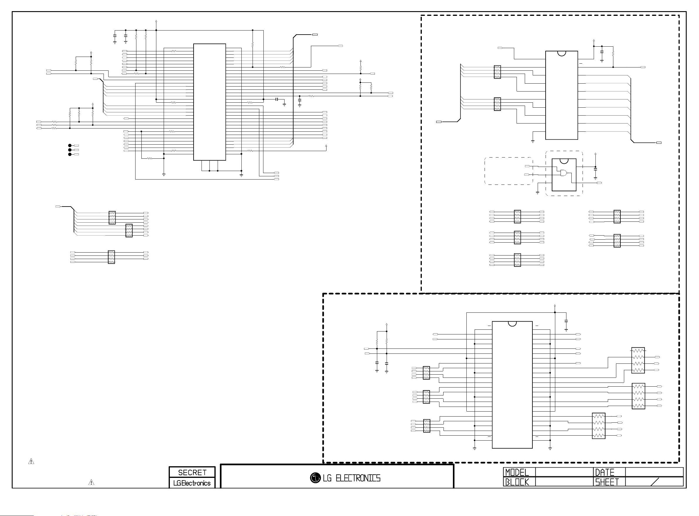
+5V_CI_ON
Copyright ⓒ 2013 LG Electronics. Inc. All right reserved.
Only for training and service purposes
LGE Internal Use Only
CI HOST I/F
PCM_RST
/PCM_WAIT
PCM_INPACK
/PCM_IORD
/PCM_IOWR
R6202
R6203
R6200
CI_IN_TS_DATA[0-7]
R6211
10K
OPT
CI
22
CI
22
OPT
22
+5V_CI_ON
R6204
10K
OPT
R6205
10K
OPT
CI_VS1
PCM_INPACK
/PCM_CE2
R6206
10K
+5V_CI_ON
R6207
10K
OPT
CI
C6200
0.1uF
CI
/CI_CD1
CI_TS_DATA[3]
CI_TS_DATA[4]
CI_TS_DATA[5]
CI_TS_DATA[6]
CI_TS_DATA[7]
/PCM_CE2
CI_VS1
CI_IN_TS_DATA[0]
CI_IN_TS_DATA[1]
CI_IN_TS_DATA[2]
CI_IN_TS_DATA[3]
CI_IN_TS_DATA[4]
CI_IN_TS_DATA[5]
CI_IN_TS_DATA[6]
CI_IN_TS_DATA[7]
CI_TS_CLK
/PCM_REG
CI_TS_VAL
CI_TS_SYNC
CI_TS_DATA[0]
CI_TS_DATA[1]
CI_TS_DATA[2]
/CI_CD2
C6201
10uF
10V
CI
R6249
R6208
10K
OPT
OPT
5V <=> 3.3V
IC904
74LVC245A
DIR
1
A0
2
A1
3
A2
4
A3
5
A4
CI
6
A5
7
A6
8
A7
9
GND
10
IC905
74LVC1G00GW
1B 5 VCC
2A
3GND
CI
AND GATE => NAND GATE
20
19
18
17
16
15
14
13
12
11
4 Y
+3.3V_NORMAL
VCC
OE
B0
B1
B2
B3
B4
B5
B6
B7
CI
+3.3V_NORMAL
CI
C903
0.1uF
16V
C904
0
0.1uF
R913
16V
OPT
EB_DATA[0]
EB_DATA[1]
EB_DATA[2]
EB_DATA[3]
EB_DATA[4]
EB_DATA[5]
EB_DATA[6]
EB_DATA[7]
DIR
/PCM_CE1
EB_DATA[0-7]
EB_DATA[0-7]
CI_ADDR[11]
CI_ADDR[9]
CI_ADDR[13]
R6243 22
C6206
0.1uF
16V
CI_ADDR[12]
CI_ADDR[7]
CI_ADDR[6]
CI_ADDR[5]
CI_ADDR[4]
CI_ADDR[3]
CI_ADDR[2]
CI_ADDR[1]
CI_ADDR[0]
CI_DATA[0-7]
OPT
+5V_CI_ON
CI_ADDR[10]
CI_ADDR[11]
CI_ADDR[9]
CI_ADDR[8]
CI_ADDR[13]
CI_ADDR[14]
CI_ADDR[12]
CI_ADDR[7]
CI_ADDR[6]
CI_ADDR[5]
CI_ADDR[4]
CI_ADDR[3]
CI_ADDR[2]
CI_ADDR[1]
CI_ADDR[0]
/PCM_CE1
+5V_CI_ON
R6245
10K
OPT
+5V_CI_ON
R6244
10K
CI
R6246
10K
/PCM_OE
OPT
/PCM_WE
/PCM_IRQA
CI_DATA[0-7]
CI_DATA[0]
CI_DATA[1]
CI_DATA[2]
CI_DATA[3]
CI_DATA[0-7]
CI_DATA[4]
CI_DATA[5]
CI_DATA[6]
CI_DATA[7]
DIR
CI
AR909
33
CI
AR910
33
WE=>OE
IOWE=>IORD
/PCM_OE
/PCM_IORD
R6209
10K
OPT
GND
/CI_DET1
100
R6214
CI
TS_OUT3
TS_OUT4
TS_OUT5
TS_OUT6
TS_OUT7
CARD_EN2
0
OPT
CI
TS_IN_SYN
TS_IN0
TS_IN1
TS_IN2
TS_IN3
TS_IN4
TS_IN5
TS_IN6
TS_IN7
TS_OUT_CLK
CI_RESET
CI_WAIT
INPACK
CI
TS_OUT_VAL
TS_OUT_SYN
TS_OUT0
TS_OUT1
TS_OUT2
/CI_DET2
IORD
IOWR
VS1
VCC
VPP
REG
GND
0
R6213
R6212 0
R6215 100
R6210
0
OPT
P6200
10120698-015LF CI
35
36
37
38
39
40
41
42
43
44
45
46
47
48
49
50
51
52
53
54
55
56
57
58
59
60
61
62
63
64
65
66
67
68
69
R6219
R6216
R6217
10K
OPT
CI_DATA[3]
CI_DATA[4]
CI_DATA[5]
CI_DATA[6]
CI_DATA[7]
CI
R6224 22
C6205 0.1uF
0
OPT
10K
OPT
CI
CI_DATA[0]
CI_DATA[1]
CI_DATA[2]
CI_IN_TS_VAL
CI_IN_TS_CLK
CI_IN_TS_SYNC
CI_ADDR[10]
CI_ADDR[8]
CI_ADDR[14]
CI
GND
1
DAT3
2
DAT4
3
DAT5
4
DAT6
5
DAT6
6
/CARD_EN1
7
ADDR10
8
/O_EN
9
ADDR11
10
ADDR10
11
ADDR8
12
ADDR13
13
ADDR14
14
/WR_EN
15
/IRQA
16
VCC
17
VPP
18
TS_IN_VAL
19
TS_IN_CLK
20
ADDR12
21
ADDR7
22
ADDR6
23
ADDR5
24
ADDR4
25
ADDR3
26
ADDR2
27
ADDR1
28
ADDR0
29
DAT0
30
DAT1
31
DAT2
32
/IO_BIT
33
GND
34
G1G2
TPO_DATA[0-7]
TPO_CLK
TPO_SOP
TPO_VAL
TPO_ERR
TPO_DATA[0]
TPO_DATA[1]
TPO_DATA[2]
TPO_DATA[3]
TPO_DATA[4]
TPO_DATA[5]
TPO_DATA[6]
TPO_DATA[7]
CI
AR904
33
AR905
CI
AR903
33
CI
33
CI_IN_TS_DATA[0]
CI_IN_TS_DATA[1]
CI_IN_TS_DATA[2]
CI_IN_TS_DATA[3]
CI_IN_TS_DATA[4]
CI_IN_TS_DATA[5]
CI_IN_TS_DATA[6]
CI_IN_TS_DATA[7]
CI_IN_TS_CLK
CI_IN_TS_SYNC
CI_IN_TS_VAL
CI_ADDR[0]
CI_ADDR[1]
CI_ADDR[2]
CI_ADDR[3]
CI_ADDR[4]
CI_ADDR[5]
CI_ADDR[6]
CI_ADDR[7]
CI_ADDR[8]
CI_ADDR[9]
CI_ADDR[10]
CI_ADDR[11]
BUFFER FOR 5V => 3.3V
/CI_CD2
/CI_CD1
+5V_NORMAL
CI
10K
R915
CI
C905
0.1uF
16V
CI
10K
R916
CI
C906
0.1uF
16V
CI_TS_DATA[7]
CI_TS_DATA[6]
CI_TS_DATA[5]
CI_TS_DATA[4]
CI_TS_DATA[3]
CI_TS_DATA[2]
CI_TS_DATA[1]
CI_TS_DATA[0]
PCM_INPACK
CI_TS_CLK
CI_TS_VAL
CI_TS_SYNC
/PCM_WAIT
/PCM_IRQA
AR921
AR920
AR919
CI
100
CI
100
CI
100
GND_8
VCC_4
GND_7
GND_6
VCC_3
GND_5
2OE
48
1A0
47
1A1
46
45
1A2
44
1A3
43
42
2A0
41
2A1
40
39
2A2
38
2A3
37
3A0
36
3A1
35
34
3A2
33
3A3
32
31
4A0
30
4A1
29
28
4A2
27
4A3
26
3OE
25
CI
AR911
33
CI
AR912
33
CI
AR913
33
IC903
74LVC16244ADGG
CI
EB_ADDR[0]
EB_ADDR[1]
EB_ADDR[2]
EB_ADDR[3]
EB_ADDR[4]
EB_ADDR[5]
EB_ADDR[6]
EB_ADDR[7]
EB_ADDR[8]
EB_ADDR[9]
EB_ADDR[10]
EB_ADDR[11]
+3.3V_NORMAL
1OE
1
1Y0
2
1Y1
3
GND_1
4
1Y2
5
1Y3
6
VCC_1
7
2Y0
8
2Y1
9
GND_2
10
2Y2
11
2Y3
12
3Y0
13
3Y1
14
GND_3
15
3Y2
16
3Y4
17
VCC_2
18
4Y0
19
4Y1
20
GND_4
21
4Y2
22
4Y3
23
4OE
24
CI_ADDR[12]
CI_ADDR[13]
CI_ADDR[14]
/PCM_REG
/PCM_OE
/PCM_WE
/PCM_IORD
/PCM_IOWR
C900
0.1uF
16V
CI
CAM_WAIT_N
CAM_IREQ_N
CAM_CD2_N
CAM_CD1_N
CAM_INPACK_N
75
AR916
CI
33
33
AR915
AR914
CI
CI
CI
AR918 75
75
TPI_DATA[3]
TPI_DATA[2]
TPI_DATA[1]
TPI_DATA[0]
EB_ADDR[12]
EB_ADDR[13]
EB_ADDR[14]
CAM_REG_N
EB_OE_N
EB_WE_N
EB_BE_N1
EB_BE_N0
CI
AR917
TPI_CLK
TPI_VAL
TPI_SOP
TPI_DATA[7]
TPI_DATA[6]
TPI_DATA[5]
TPI_DATA[4]
THE SYMBOL MARK OF THIS SCHEMETIC DIAGRAM INCORPORATES
SPECIAL FEATURES IMPORTANT FOR PROTECTION FROM X-RADIATION.
FILRE AND ELECTRICAL SHOCK HAZARDS, WHEN SERVICING IF IS
ESSENTIAL THAT ONLY MANUFATURES SPECFIED PARTS BE USED FOR
THE CRITICAL COMPONENTS IN THE SYMBOL MARK OF THE SCHEMETIC.
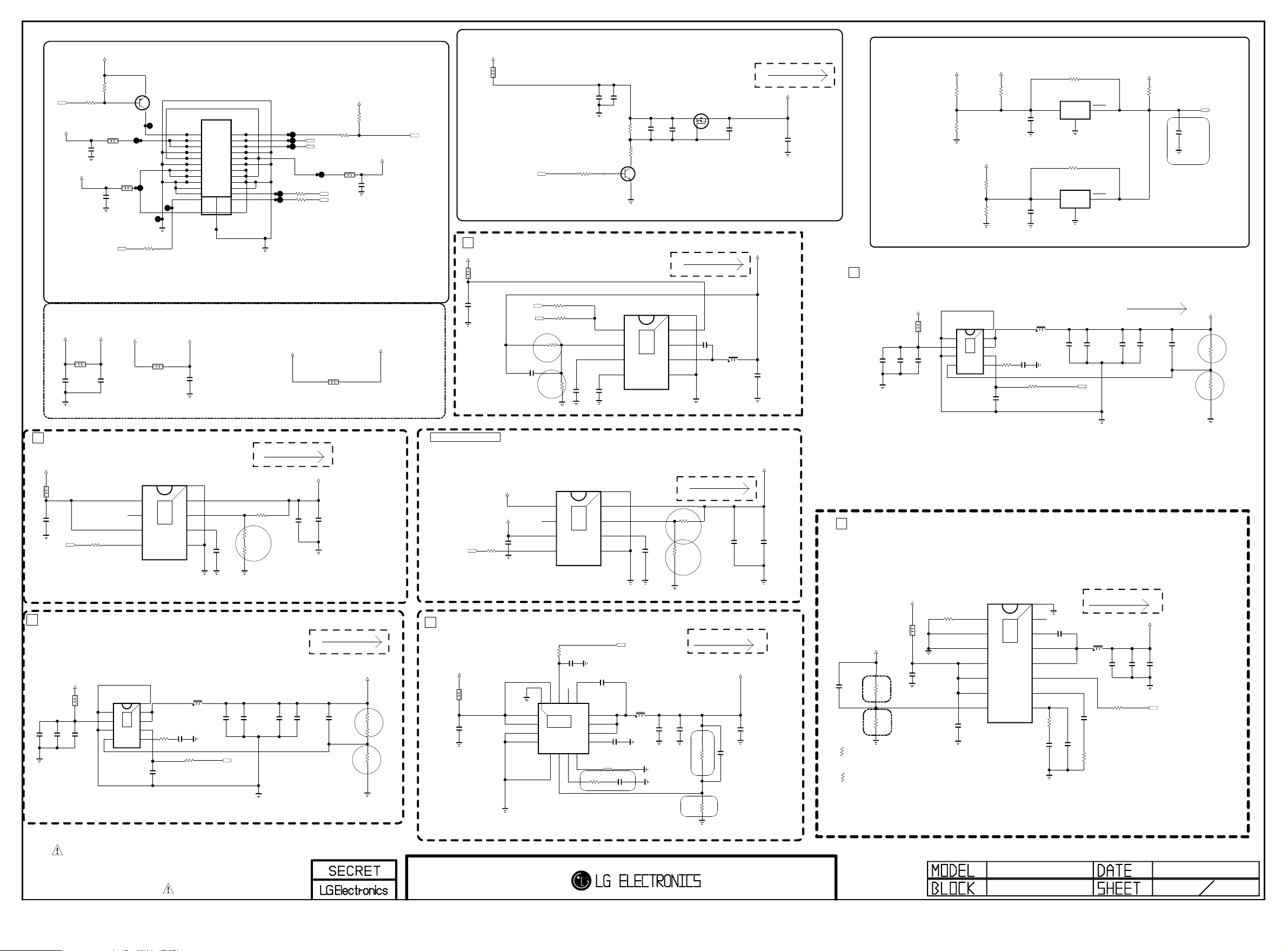
+3.5V_ST
Copyright ⓒ 2013 LG Electronics. Inc. All right reserved.
Only for training and service purposes
LGE Internal Use Only
R2305
RL_ON
10K
+3.5V_ST
+12V
C2306
0.1uF
L/DIM0_MOSI
BLM18SG121TN1D
C2307
0.1uF
16V
50V
eMMC POWER
+3.3V_NORMAL
3.3V_EMMC
L2319
BLM18PG121SN1D
C2371
0.1uF
16V
10K
R2306
L2303
CIS21J121
+1.8V_NORMAL
C2372
0.1uF
16V
L2302
2
1
Q2301 MMBT3906(NXP)
3
G3S
R2367
33
L2306
BLM18PG121SN1D
PWR ON
3.5V
3.5V
L/DIM0_MOSI
EMMC_VCCQ
POWER_18P
1
1
3
3
5
5
GND
7
7
24V
9
9
GND
11
11
12V
13
13
12V
15
15
GND
17
17
GND
19
GND
21
23
POWER_24P
SMAW200-H18S1
C2376
22uF
10V
SAMSUNG_eMMC
P2301
SMAW200-H24S2
INV ON
2
2
PDIM#1
4
4
PDIM#2
6
6
GND
8
8
24V
10
10
GND
12
12
12V
14
14
24V
16
16
GND
18
18
GND
20
L/DIMO_VS
22
19
L/DIM0_SCLK
24
25
P2300
+3.3V_TU
G3S
R2368
33
G3S
R2369
33
PWM_DIM
PWM_DIM2
L/DIM0_VS
L/DIM0_SCLK
L2314
BLM18PG121SN1D
R2312
100
L2305
CIS21J121
C2317
0.1uF
50V
+3.3V_NORMAL
R2330
1K
+24V
+3.3V_TU_IN
@netLa
INV_CTL
+12V
L2311
CIS21J121
1
+12V
L2310
BLM18PG121SN1D
C2322
10uF
16V
Switching freq: 700K
PANEL_POWER
PANEL_CTL
+5V_Normal
R2301
10KPOWER_ON/OFF1
POWER_ON/OFF2_1
R1
C2334
100pF
50V
R2
1%
R2308
R2311
OPT
R2348
10K
56K
10K
1%
C2326
0.01uF
50V
R2341
10K
C2336
1uF
10V
C2328
0.1uF
VREG5
C2342
2200pF
50V
VFB
50V
R2343
33K
R2344
5.6K
C
Q2304
B
MMBT3904(NXP)
E
IC2304
TPS54327DDAR
EN
1
2
3
SS
4
3A
C2332
10uF
9
THERMAL
16V
8
7
6
5
C2335
0.1uF
50V
[EP]GND
VIN
VBST
SW
GND
AO3407A
OPT
Q2305
Vout=0.765*(1+R1/R2)
S
G
MAX 1A
C2345
0.1uF
16V
D
L2313
6.8uH
NR8040T4R7N
1uF
C2339
OPT
Power_DET
TYP 1450mA
PANEL_VCC
25V
+5V_NORMAL
C2346
0.1uF
50V
+12V
4
+12V
C2343
22uF
10V
L2307
BLM18PG121SN1D
Placed on SMD-TOP
C2305
C2303
10uF
10uF
16V
16V
C2318
0.1uF
16V
OPT
BD86106EFJ
PGND
VIN
AGND
FB
PD_+12V
R2362
2.7K
1%
PD_+12V
R2363
1.2K
1%
IC2306
1
2
3
4
6A
THERMAL
+24V
+3.5V_ST
PD_24V
R2364
8.2K
1%
PD_24V
R2365
1.5K
1%
PD_+3.5V
R2366
0
5%
C2359
0.1uF
16V
C2360
0.1uF
16V
VCC
VCC
PD_24V
R2373
100K
IC2307
NCP803SN293
3
1
GND
PD_24V
R2372
100K
PD_24V
IC2308
NCP803SN293
3
1
GND
+3.5V_ST
R2376
10K
RESET
2
RESET
2
OPT
POWER_DET
C2365
0.1uF
16V
not to RESET at 8kV ESD
24V-->3.48V
12V-->3.58V
ST_3.5V-->3.5V
+1.0V_VDD
LG1152 Max: 1728 mA
LG1132 Max: 2000 mA
C2356
47pF
50V
OPT
+1.0V_VDD
R2313
2.7K
R2318
7.5K
1/16W
5%
1%
R1
R2
L2309
C2321
0.0068uF
50V
R2310
10K
2uH
POWER_ON/OFF2_3
C2352
10uF
10V
C2353
10uF
10V
C2354
10uF
10V
C2355
10uF
10V
[EP]
SW_2
8
SW_1
9
7
EN
6
R2309
6.8K
COMP
5
C2319
0.1uF
16V
1
+3.5V_ST
L2301
BLM18PG121SN1D
C2301
4.7uF
10V
R2300
10K
POWER_ON/OFF1
Vout=0.8*(1+R1/R2)
2
+3.3V_NORMAL
+12V
L2300
BLM18PG121SN1D
Placed on SMD-TOP
C2304
C2300
10uF
10uF
16V
16V
C2309
0.1uF
16V
OPT
BD86106EFJ
PGND
VIN
AGND
FB
+1.8V
THERMAL
IC2300
[EP]
IN
1
PG
2
VCC
3
EN
4
9
THERMAL
OUT
8
FB
7
SS
6
GND
5
1.5A
L2304
C2311
0.0068uF
50V
R2303
10K
2uH
POWER_ON/OFF2_1
[EP]
SW_2
8
SW_1
9
7
EN
6
R2302
6.8K
COMP
5
C2310
0.1uF
16V
AP7173-SPG-13 HF(DIODES)
IC2301
1
2
3
4
6A
Vout=0.8*(1+R1/R2)
C2308
2200pF
50V
C2312
10uF
10V
R2314
3K
1%
R2315
100
1%
C2314
10uF
10V
1/16W
3.9K
R2321
R2
3. soft start
293 mA
+1.8V_NORMAL
+3.3V_NORMAL
1%
R1
C2313
10uF
10V
C2315
0.1uF
16V
POWER_ON/OFF2_2
4
+5V_NORMAL
R2334
10K
DDR MAIN 1.5V
MAX 4.7 A
+3.3V_NORMAL
+3.5V_ST
L2308
C2316
10uF
10V
C2323
10uF
10V
C2351
47pF
50V
OPT
R2304
R2316
30K
R2317
10K
1%
2K
1/16W
1%
C2320
R1
1%
10uF
10V
R2
+2.5V
IN
PG
VCC
EN
EP[GND]
1
THERMAL
2
3
TPS54319TRE
4
5
AGND
10K
R2339
17
IC2302
3A
3A
1
2
3
1.5A
4
C2325
6
COMP
VSENSE
IC2303
THERMAL
0.1uF
16V
BOOT14PWRGD15EN16VIN_3
13
7
8
RT/CLK
9
12
11
10
9
R2340
15K
1/16W 5%
$ 0.145
AP7173-SPG-13 HF(DIODES)
C2324
10uF
10V
Vout=0.8*(1+R1/R2)
VIN_1
VIN_2
GND_1
GND_2
PH_3
PH_2
PH_1
SS/TR
8
7
6
5
C2327
0.1uF
16V
[EP]
OUT
FB
SS
GND
0.01uF
R2342
330K1/16W 5%
C2329
50V
4700pF
C2330
50V
C2331
2200pF
50V
POWER_ON/OFF2_3
L2312
3.6uH
NR8040T3R6N
C2333
22uF
10V
C2337
22uF
10V
R2347
4.3K
1%
R2346
2K
1%
R1
R2
R2
R1
R2350
56K
1/16W
1%
700 mA
1074 mA
R2349
47K 1%
+1.5V_DDR
C2338
100pF
50V
+2.5V_NORMAL
C2340
10uF
10V
C2341
0.1uF
16V
C2344
0.1uF
16V
4
C2375
180pF
50V
R2378-*1
8.2K
1/16W
R2379-*1
15K
+12V
L2315
+0.9V_VDD
C2347
10uF
16V
R1
R2378
6.8K
1/16W
1%
FRC3
R2
R2379
12K
1/16W
1%
FRC3
URSA5
1%
URSA5
1/16W
1%
Vout=0.6*(1+R1/R2)
Vout=0.8*(1+R1/R2)
IC2305
EAN62348501
R2377
RT/CLK
100K
1/16W
5%
C2302
4.7uF
16V
GND_1
GND_2
PVIN_1
PVIN_2
VSENSE
1
15
2
THERMAL
3
4
5
VIN
6
7
[EP]GND
PWRGD
14
C2349
BOOT
13
0.1uF
16V
PH_2
12
PH_1
11
EN
10
SS/TR
9
COMP
8
1.3K
R2307
C2348
4700pF 50V
47pF 50V
22000pF 50V
C2373
R2381 0
Max 5926 mA
L2317
1uH
R2357 1K
C2374
1/16W
5%
Switching freq: 400 ~ 580 Khz
+0.9V_VDD
C2363
C2350
22uF
22uF
10V
10V
POWER_ON/OFF2_3
OPT
C2370
10uF
10V
Vout=0.827*(1+R1/R2)=1.521V
THE SYMBOL MARK OF THIS SCHEMETIC DIAGRAM INCORPORATES
SPECIAL FEATURES IMPORTANT FOR PROTECTION FROM X-RADIATION.
FILRE AND ELECTRICAL SHOCK HAZARDS, WHEN SERVICING IF IS
ESSENTIAL THAT ONLY MANUFATURES SPECFIED PARTS BE USED FOR
THE CRITICAL COMPONENTS IN THE SYMBOL MARK OF THE SCHEMETIC.
LG1152
POWER
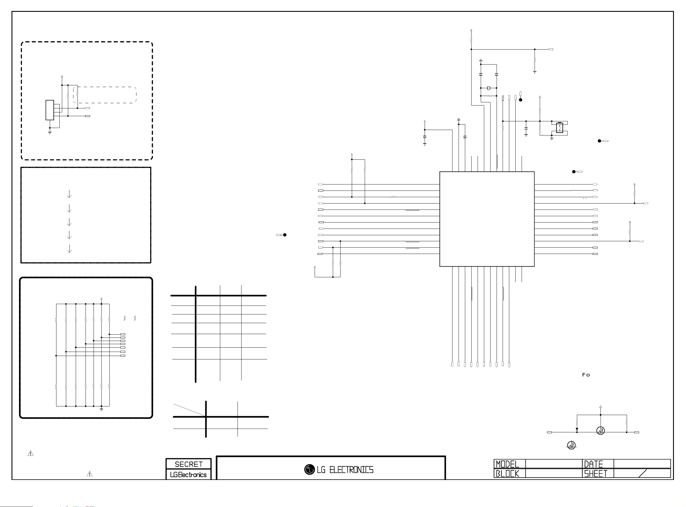
Renesas MICOM
Copyright ⓒ 2013 LG Electronics. Inc. All right reserved.
Only for training and service purposes
LGE Internal Use Only
For Debug
+3.3V_NORMAL
R3035
4.7K
OPT
HDMI_WAUP:HDMI_INIT
10K
12V_EXT_PWR_DET
+3.5V_ST
MICOM_DEBUG
P3000
12507WS-04L
5
1
2
3
4
Don’t remove R3014,
not making float P40
R3014 1K
R3011 10K
MICOM_DEBUG
MICOM_DEBUG
MICOM_RESET
GP4 High/MID Power SEQUENCE
POWER_ON/OFF!
POWER_ON/OFF2_1
POWER_ON/OFF2_2
POWER_ON/OFF2_3
POWER_ON/OFF2_4
SOC_RESET
MICOM MODEL OPTION
+3.5V_ST
MICOM_GED
R3016 10K
MICOM_MHL
R3020 10K
MICOM_PDP
R3030 10K
MICOM_GP4_10PIN
R3007 10K
R3005 10K
MICOM_TOUCH_KEY
R3009 10K
MICOM_JAPAN
R3005-*1
R3012 10K
MICOM_OLED_MAIN
MICOM_LOGO_LIGHT
R3005-*2
56K
MICOM_OLED_FRC
MODEL1_OPT_0
MODEL1_OPT_1
MODEL1_OPT_2
MODEL1_OPT_3
MODEL1_OPT_4
MODEL1_OPT_5
MODEL1_OPT_6
R3000
LOGO_LIGHT
+3.5V_ST
10K
R3026
C3004
0.1uF
R3027
16V
P120/ANI19
37
P140/PCLBUZ0/INTP6
36
P00/TI00/TXD1
35
P01/TO00/RXD1
34
P130
33
P20/ANI0/AVREFP
32
P21/ANI1/AVREFM
31
P22/ANI2
30
P23/ANI3
29
P24/ANI4
28
P25/ANI5
27
P26/ANI6
26
P27/ANI7
25
24
MICOM_RESET_SW
OPT
270K
SW3000
JTP-1127WEM
4 3
12
12V_EXT_PWR_DET
POWER_ON/OFF2_4
+3.3V_NORMAL
+3.3V_NORMAL
R3036
10K
OPT
R3037
10K
OPT
POWER_ON/OFF2_1
SIDE_HP_MUTE
RL_ON
SCART_MUTE
POWER_ON/OFF2_4
KEY2
KEY1
MODEL1_OPT_2
MODEL1_OPT_1
MODEL1_OPT_0
MODEL1_OPT_4
MODEL1_OPT_3
MICOM MODEL OPTION
POWER_ON/OFF2_3
I2C_SCL3
I2C_SDA3
AMP_RESET_N
PANEL_CTL
MODEL1_OPT_5
HDMI_CEC
POWER_ON/OFF2_2
POWER_ON/OFF2_3
EYE_SDA
EYE_SCL
MODEL1_OPT_6
+3.5V_ST
AMP_RESET_BY_MICOM
IR
R3001
3.3K
R3032
R3002
3.3K
EYE_Q_10P
+3.3V_NORMAL
10K
R3033
10K
R3003 22
AMP_RESET_BY_MICOM
P31/TI03/TO03/INTP4
P75/KR5/INTP9/SCK01/SCL01
P74/KR4/INTP8/SI01/SDA01
P71/KR1/SI21/SDA21
P70/KR0/SCK21/SCL21
P30/INTP3/RTC1HZ/SCK11/SCL11
EYE_Q_10P
+3.5V_ST
C3000
0.1uF
P60/SCLA0
P61/SDAA0
P62
P63
P73/KR3/SO01
P72/KR2/SO21
1
2
3
4
5
6
7
8
9
10
11
12
GND
C3001 0.47uF
REGC
VSS
VDD
46
47
48
R5F100GEAFB#30
13
14
15
8pF
C3002
X3000
32.768KHz
R3023
4.7M
OPT
P123/XT1
P137/INTP0
P122/X2/EXCLK
P121/X1
42
43
44
45
IC3000
MICOM
16
17
18
19
C3003 8pF
MICOM_DEBUG
LOGO_LIGHT
MICOM_RESET
R3024 22
P41/TI07/TO07
P40/TOOL0
RESET
P124/XT2/EXCLKS
38
39
40
41
20
21
22
23
P146
10
P147/ANI18
P10/SCK00/SCL00
/ OLED
LOGO_LIGHT
JAPAN
TOUCH_KEY
PDP
IR Wafer
10Pin
(GP4_TOOL)
MHLMODEL_OPT_5
GEDMODEL_OPT_6
For LM86
For JAPAN
For Sample Set
GP4_HIGH
P17/TI02/TO02
P51/INTP2/SO11
P50/INTP1/SI11/SDA11
P16/TI01/TO01/INTP5
P13/TXD2/SO20
P14/RXD2/SI20/SDA20
P12/SO00/TXD0/TOOLTXD
P15/PCLBUZ1/SCK20/SCL20
P11/SI00/RXD0/TOOLRXD/SDA00
MODEL_OPT_0
MODEL_OPT_1
22K
MODEL_OPT_2
MODEL_OPT_3
MODEL_OPT_4
NON LOGO_LIGHT
NON JAPAN
TACT_KEY
LCD
IR Wafer
12/15Pin
(GP3_Soft touch)
NON_MHL
NON_GED
R3006 10K
R3008 10K
R3010 10K
R3021 10K
R3017 10K
MICOM_NON_MHL
MICOM_NON_GED
R3031 10K
MICOM_LCD/OLED
MICOM_GP3_12/15PIN
MICOM_TACT_KEY
R3013 10K
MICOM_NON_JAPAN
MICOM_NON_LOGO_LIGHT
THE SYMBOL MARK OF THIS SCHEMETIC DIAGRAM INCORPORATES
SPECIAL FEATURES IMPORTANT FOR PROTECTION FROM X-RADIATION.
FILRE AND ELECTRICAL SHOCK HAZARDS, WHEN SERVICING IF IS
ESSENTIAL THAT ONLY MANUFATURES SPECFIED PARTS BE USED FOR
THE CRITICAL COMPONENTS IN THE SYMBOL MARK OF THE SCHEMETIC.
Eye Sensor Option
MODEL_OPT_4
MODEL_OPT_2
0
1
0
N/A
CM3231_CAPELLA
(GP3 Soft touch) (GP4 Soft touch)
1
MC8101_ABOV
(TACT_KEY)
CM3231_CAPELLA
POWER_DET
POWER_ON/OFF1
WOL/WOW_POWER_ON
LED_R
WOL_CTL
INV_CTL
SOC_RESET
SOC_TX
SOC_RX
AMP_MUTE
CEC_REMOTE
MICOM
D3000
BAT54_SUZHO
D
For CEC
R3028
27K
G
Q3001-*1
SI1012CR-T1-GE3
S
HDMI_CEC_FET_VISHAY
+3.5V_ST
G
D
Q3001
RUE003N02
HDMI_CEC_FET_ROHM
R3029
120K
S
HDMI_CEC
2011.12.12
30
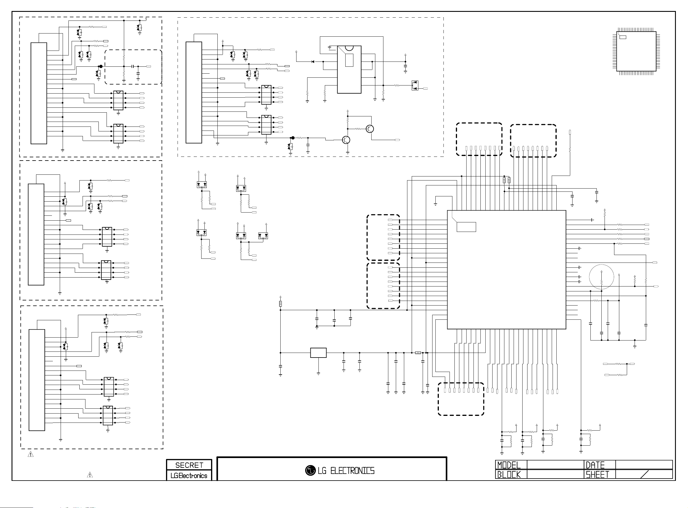
BODY_SHIELD
Copyright ⓒ 2013 LG Electronics. Inc. All right reserved.
Only for training and service purposes
LGE Internal Use Only
20
HP_DET
19
5V
18
GND
17
DDC_DATA
16
DDC_CLK
15
ARC
14
CE_REMOTE
13
CK-
12
CK_GND
11
CK+
10
D0-
9
D0_GND
8
EAG62611204
51U019S-312HFN-E-R-B-LG
EAG62611204
51U019S-312HFN-E-R-B-LG
EAG62611204
51U019S-312HFN-E-R-B-LG
JK3202
BODY_SHIELD
20
19
18
17
16
15
14
13
12
11
10
9
8
7
6
5
4
3
2
1
JK3200
BODY_SHIELD
20
19
18
17
16
15
14
13
12
11
10
9
8
7
6
5
4
3
2
1
JK3201
D0+
7
D1-
6
D1_GND
5
D1+
4
D2-
3
D2_GND
2
D2+
1
HP_DET
5V
GND
DDC_DATA
DDC_CLK
NC
CE_REMOTE
CK-
CK_GND
CK+
D0-
D0_GND
D0+
D1-
D1_GND
D1+
D2-
D2_GND
D2+
HP_DET
5V
GND
DDC_DATA
DDC_CLK
NC
CE_REMOTE
CK-
CK_GND
CK+
D0-
D0_GND
D0+
D1-
D1_GND
D1+
D2-
D2_GND
D2+
ESD_HDMI
5V_HDMI_2
5V_HDMI_3
VA3206
VA3209
ESD_HDMI
CEC_REMOTE
VA3214
ESD_HDMI
R3250
VA3208
ESD_HDMI
R3207 100
R3208 100
VA3213
ESD_HDMI
CEC_REMOTE
ESD_HDMI
CEC_REMOTE
100
HDMI_HPD_1
DDC_SDA_1
DDC_SCL_1
VA3207
ESD_HDMI
D3213
1 8
2 7
3 6
4 5
ESD_HDMI
D3212
1 8
2 7
3 6
4 5
ESD_HDMI
HDMI1 With ARC
R3251
100
VA3205
ESD_HDMI
R3209 100
R3210 100
VA3203
VA3204
ESD_HDMI
D3211
1 8
2 7
3 6
ESD_HDMI
4 5
9
D3209
1 8
2 7
3 6
ESD_HDMI
4 5
9
R3252
100
VA3202
ESD_HDMI
VA3201
VA3200
ESD_HDMI
D3208
1 8
2 7
3 6
ESD_HDMI
4 5
9
D3210
1 8
2 7
3 6
ESD_HDMI
4 5
9
R3248
1K
OPT
C3202
1uF
10V
R3249
3.9K
OPT
9
9
DDC_SDA_2
DDC_SCL_2
CK-_HDMI2
CK+_HDMI2
D0-_HDMI2
D0+_HDMI2
D1-_HDMI2
D1+_HDMI2
D2-_HDMI2
D2+_HDMI2
HDMI2
R3204 100
R3205 100
ESD_HDMI
CK-_HDMI3
CK+_HDMI3
D0-_HDMI3
D0+_HDMI3
HDMI3
C3226
0.1uF
16V
HDMI_HPD_2
D1-_HDMI3
D1+_HDMI3
D2-_HDMI3
D2+_HDMI3
5V_HDMI_1
VA3215
ESD_HDMI
ARC
SPDIF_OUT_ARC
OPT
CK-_HDMI1
CK+_HDMI1
D0-_HDMI1
D0+_HDMI1
D1-_HDMI1
D1+_HDMI1
D2-_HDMI1
D2+_HDMI1
HDMI_HPD_3
DDC_SDA_3
DDC_SCL_3
BODY_SHIELD
GND
20
HP_DET
19
5V
18
GND
17
DDC_DATA
16
DDC_CLK
15
NC
14
CE_REMOTE
13
CK-
12
CK_GND
11
CK+
10
D0-
9
D0_GND
8
EAG62611204
51U019S-312HFN-E-R-B-LG
JK3203
+5V_NORMAL
D3200
R3217
47K
+5V_NORMAL
D3201
R3218
47K
D0+
7
D1-
6
D1_GND
5
D1+
4
D2-
3
D2_GND
2
D2+
1
5V_HDMI_1
5V_HDMI_3
A2CA1
R3219
47K
A2CA1
R3220
47K
5V_HDMI_4
VA3216
ESD_HDMI
DDC_SDA_1
DDC_SCL_1
DDC_SDA_3
DDC_SCL_3
CEC_REMOTE
+5V_NORMAL
D3202
R3225
47K
+5V_NORMAL
D3203
R3226
47K
VA3210
ESD_HDMI
VA3212
ESD_HDMI
5V_HDMI_2
A2CA1
5V_HDMI_4
A2CA1
R3228
47K
D3205
R3229
47K
R3253
100
R3222
R3223 100
VA3211
ESD_HDMI
D3214
1 8
2 7
ESD_HDMI
3 6
4 5
9
D3215
1 8
2 7
ESD_HDMI
3 6
4 5
9
DDC_SDA_2
DDC_SCL_2
+3.5V_ST
A2CA1
DDC_SDA_4
DDC_SCL_4
C3200
10uF
10V
HDMI_HPD_4
100
+3.3V_NORMAL
L3200
BLM18PG121SN1D
DDC_SDA_4
DDC_SCL_4
CK-_HDMI4
CK+_HDMI4
D0-_HDMI4
D0+_HDMI4
D1-_HDMI4
D1+_HDMI4
D2-_HDMI4
D2+_HDMI4
D3207
5V_HDMI_4
MBR230LSFT1G
R3243
1K
1/16W
5%
5.6V
Limit 0.8A
[EP]
R3200
IC3200
3
FAULT
OUT_2
OUT_1
ILIM0
ILIM1
62K
1/10W
OPT
Limit 0.8A
Q3200
MMBT3904(NXP)
C3205
10uF
10V
OUT
2
1
GND/ADJ
R3201
D3206
30V
62K
1/10W
C3223
0.047uF
25V
AZ1117BH-1.2TRE1
IN
IC3202
TPS2554
GND
THERMAL
11
+3.5V_ST
R3246
10K
C
E
C3203
10uF
10V
R3247
10K
C3211
0.1uF
16V
1
IN_1
2
IN_2
3
ILIM_SEL
4
EN
5
5%
E
MMBT3906(NXP)
Q3201
B
C
HDMI4 With MHL
HDMI2
CK-_HDMI2
CK+_HDMI2
D0-_HDMI2
D0+_HDMI2
D1-_HDMI2
D1+_HDMI2
D2-_HDMI2
D2+_HDMI2
HDMI3
CK-_HDMI3
CK+_HDMI3
D0-_HDMI3
D0+_HDMI3
D1-_HDMI3
D1+_HDMI3
D2-_HDMI3
D2+_HDMI3
C3201
10uF
10V
1/16W
C3210
0.1uF
16V
10
9
8
7
6
B
Vout=0.8*(1+R1/R2)
220K
R3206
C3204
0.1uF
16V
1/16W
10K
R3245
+5V_NORMAL
5%
MHL_DET
C3206
0.1uF
16V
C3207
0.1uF
16V
C3208
0.1uF
C
D3204
A1
A2
L3201
BLM18PG121SN1D
C3216
10uF
10V
MHL_DET
R1XCN
R1XCP
R1X0N
R1X0P
R1X1N
R1X1P
R1X2N
R1X2P
AVDD12_1
VDD12_1
R3XCN
R3XCP
R3X0N
R3X0P
R3X1N
R3X1P
R3X2N
R3X2P
AVDD12_2
VDD33_1
R4XCN
R4XCP
C3217
0.1uF
16V
HDMI1
D1-_HDMI1
D0+_HDMI1
D1+_HDMI1
D2-_HDMI1
D2+_HDMI1
R0X0N
R0X0P
R0X1N
R0X1P
R0X2N
R0X2P
AVDD12_3
VDD33_2
[EP]GND
81
82
83
84
85
86
87
88
1
2
THERMAL
3
89
4
5
6
7
8
9
10
SII9587CNUC
11
12
13
14
Device Address : 0XB0
15
16
17
18
19
20
21
22
23
R4X0N24R4X0P25R4X1N26R4X1P27R4X2N28R4X2P
D1-_HDMI4
D0+_HDMI4
D0-_HDMI4
CK+_HDMI4
CK-_HDMI4
D2-_HDMI4
D1+_HDMI4
HDMI4
29
VDD12_2
D2+_HDMI4
30
DSDA031DSCL0
DDC_SDA_1
CK-_HDMI1
D0-_HDMI1
CK+_HDMI1
R0XCN
R0XCP
79
80
IC3201
FHD
32
CBUS_HPD0
DDC_SCL_1
HDMI_HPD_1
L3202
L3203
TCVDD12
TPVDD12
77
78
33
34
DSDA135DSCL1
R0PWR5V
DDC_SDA_2
5V_HDMI_1
R3231
10
C3213
1uF
HDMI S/W OUTPUT
HDMI_RX0-
HDMI_RX0+
HDMI_CLK-
HDMI_CLK+
TX0P
TX0N
TXCP
TXCN
73
74
75
76
36
37
38
DSDA339DSCL3
R1PWR5V
CBUS_HPD1
DDC_SCL_2
DDC_SDA_3
HDMI_HPD_2
5V_HDMI_2
R3232
10
1/16W
C3214
R3233
5.1K
1uF
5%
HDMI_RX1-
HDMI_RX1+
TX1P
TX1N
71
72
40
CBUS_HPD3
DDC_SCL_3
HDMI_HPD_3
1/16W
R3234
5.1K
5%
HDMI_RX2-
HDMI_RX2+
ARC69TX2P
TX2N
70
41
42
DSDA443DSCL4
R3PWR5V
DDC_SDA_4
5V_HDMI_3
R3240
10
C3220
1uF
VDD12_3
67
68
66
65
64
63
62
61
60
59
58
57
56
55
54
53
52
51
50
49
48
47
46
45
44
CBUS_HPD4
DDC_SCL_4
HDMI_HPD_4
1/16W
R3241
5.1K
5%
SPDIF_OUT_ARC
R3221
10
OPT
C3224
0.1uF
16V
RSVDL
SPDIF_IN
INT
CSCL
CSDA
RESET_N
TPWR
GPIO1
GPIO0
CD-SENSE4
CD_SENSE3
GPIO2
CD_SENSE1
CD_SENSE0
WKUP
LPSBV
PWRMUX_OUT
SBVCC5
R5PWR5V[VGA]
DSCL5[VGA]
DSDA5[VGA]
R4PWR5V
C3219
1uF
16V
0.1uF
C3225
HDMI_WKUP
5V_HDMI_4
R3238
10
+3.3V_NORMAL
+3.5V_ST
R3216
10
C3209
0.1uF
16V
MHL_DET
1/16W
R3239
5.1K
5%
1/16W
R3213
5.1K
5%
C3212
1uF
10V
UD
R1XCN
R1XCP
R1X0N
R1X0P
R1X1N
R1X1P
R1X2N
R1X2P
AVDD12_1
VDD12_1
R3XCN
R3XCP
R3X0N
R3X0P
R3X1N
R3X1P
R3X2N
R3X2P
AVDD12_2
VDD33_1
R4XCN
R4XCP
10K
R3202
R3224 33
R3211 33
R3236 33
R3237 33
R3214 33
+5V_NORMAL
C3215
0.1uF
16V
OPT
R3215 33
R3212 33
[EP]GND
1
2
THERMAL
3
4
5
6
7
8
9
10
11
12
13
14
15
16
17
18
19
20
21
22
23
R4X0N24R4X0P25R4X1N26R4X1P27R4X2N28R4X2P
OPT
C3218
10uF
10V
89
IC3201-*1
SII9587CNUC-3
29
30
DSDA031DSCL0
VDD12_2
+3.3V_NORMAL
32
33
34
36
37
38
40
DSDA135DSCL1
DSDA339DSCL3
R0PWR5V
R1PWR5V
CBUS_HPD0
CBUS_HPD1
CBUS_HPD3
10K
R3203
12V_EXT_PWR_DET
VDD12_368ARC69TX2P70TX2N71TX1P72TX1N73TX0P74TX0N75TXCP76TXCN77TCVDD1278TPVDD1279R0XCN80R0XCP81R0X0N82R0X0P83R0X1N84R0X1P85R0X2N86R0X2P87AVDD12_388VDD33_2
67
RSVDL
66
SPDIF_IN
65
INT
64
CSCL
63
CSDA
62
RESET_N
61
TPWR
60
GPIO1
59
GPIO0
58
CD-SENSE4
57
CD_SENSE3
56
GPIO2
55
CD_SENSE1
54
CD_SENSE0
53
WKUP
52
LPSBV
51
PWRMUX_OUT
50
SBVCC5
49
R5PWR5V[VGA]
48
DSCL5[VGA]
47
DSDA5[VGA]
46
R4PWR5V
45
41
42
44
DSDA443DSCL4
R3PWR5V
CBUS_HPD4
SPDIF_OUT
HDMI_INT
I2C_SCL5
I2C_SDA5
HDMI_S/W_RESET
MHL_DET
10K
R3244
HDMI_WKUP
C3222
10uF
10V
THE SYMBOL MARK OF THIS SCHEMETIC DIAGRAM INCORPORATES
SPECIAL FEATURES IMPORTANT FOR PROTECTION FROM X-RADIATION.
FILRE AND ELECTRICAL SHOCK HAZARDS, WHEN SERVICING IF IS
ESSENTIAL THAT ONLY MANUFATURES SPECFIED PARTS BE USED FOR
THE CRITICAL COMPONENTS IN THE SYMBOL MARK OF THE SCHEMETIC.
GP4
2011.10.19
HDMI 32

CVBS 1 PHONE JACK
Copyright ⓒ 2013 LG Electronics. Inc. All right reserved.
Only for training and service purposes
LGE Internal Use Only
JK3800
KJA-PH-1-0177-1
5 M5_GND
4 M4
3 M3_DETECT
1 M1
6 M6
D3800
5.6V
OPT
D3801
5.6V
+3.3V_NORMAL
D3806
C3805
5.6V
18pF
OPT
R3810
10K
OPT
50V
ESD_MTK
AV1_CVBS_DET
AV1_CVBS_IN
AV1_L_IN
COMPONENT 1 PHONE JACK
JK3801
KJA-PH-1-0177-2
5 M5_GND
4 M4
3 M3_DETECT
1 M1
6 M6
D3803
5.6V
OPT
+3.3V_NORMAL
Close to the jack
C3804
D3807
18pF
5.6V
R3806
10K
50V
OPT
ESD_MTK
COMP1_DET
COMP1_Y
COMP1_Pb
HP_LOUT
HP_ROUT
HEADPHONE
HP_DET
+3.3V_NORMAL
R3700
10K
HP_OUT
OPT
VA3700
5.6V
JK3700
KJA-PH-0-0177
5GND
4L
3DETECT
1R
EAG61030001
HP_JK
SOC_RX
SOC_TX
RS232C
D3802
5.6V
AV1_R_IN
OPT
COMP1_Pr
SPDIF OUT
+3.5V_ST
P3800
12507WS-04L
1
2
3
4
5
SPDIF_OUT
D3613-*1
5.5V
ADUC 5S 02 0R5L
ESD_MTK
R3620
2.7K
R3615
33
D3613
5.5V
ADUC 5S 02 0R5L
OPT
OPT
+3.3V_NORMAL
C3615
0.1uF
16V
JK3602
2F11TC1-EM52-4F
VIN
A
VCC
B
GND
C
Fiber Optic
4
SHIELD
ESD For MTK ESD For LG1152
D3803-*1
5.6V
ESD_MTK
D3800-*1
5.6V
ESD_MTK
D3801-*1
5.6V
ESD_MTK
D3802-*1
5.6V
ESD_MTK
THE SYMBOL MARK OF THIS SCHEMETIC DIAGRAM INCORPORATES
SPECIAL FEATURES IMPORTANT FOR PROTECTION FROM X-RADIATION.
FILRE AND ELECTRICAL SHOCK HAZARDS, WHEN SERVICING IF IS
ESSENTIAL THAT ONLY MANUFATURES SPECFIED PARTS BE USED FOR
THE CRITICAL COMPONENTS IN THE SYMBOL MARK OF THE SCHEMETIC.
D3803-*2
5.6V
ESD_LG1152
D3800-*2
ESD_LG1152
D3801-*2
5.6V
ESD_LG1152
D3802-*2
5.6V
ESD_LG1152
5.6V
VA3700-*1
5.6V
ESD_MTK_HP_OUT
ESD for LG1152ESD for MTK
VA3700-*2
5.6V
ESD_LG1152_HP_OUT
JACK_COMMON
2011.11.21
38
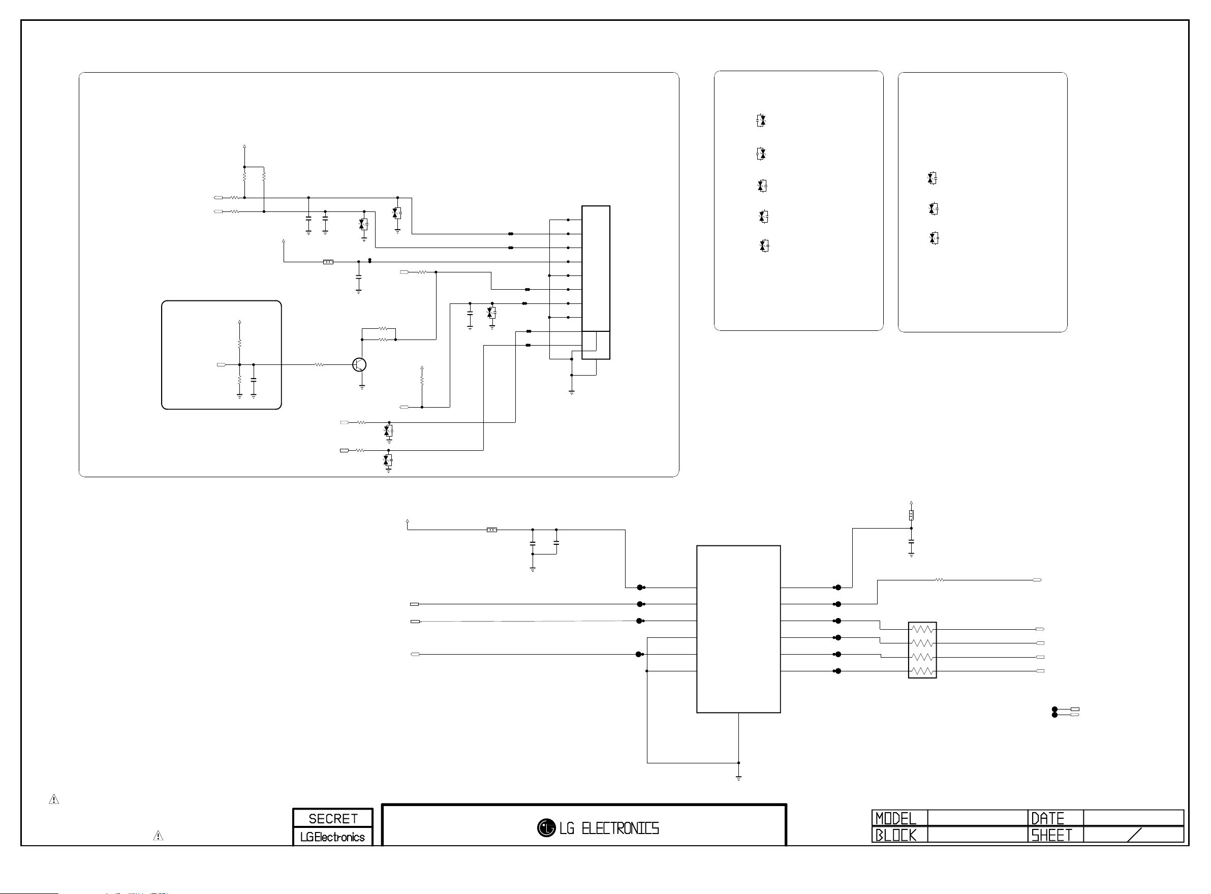
ESD for MTK
Copyright ⓒ 2013 LG Electronics. Inc. All right reserved.
Only for training and service purposes
LGE Internal Use Only
ESD for LG1152
IR & KEY & LOGO
KEY1
KEY2
Place Near Micom
LOGO_LIGHT
+3.5V_ST
R4117
10K
5%
R4113
100
R4114
100
+3.5V_ST
R4105
10K
LOGO_LIGHT
R4118
10K
5%
10K
OPT
R4104
LOGO_LIGHT
C4103
0.1uF
16V
+3.5V_ST
C4100
0.1uF
0.1uF
L4100
BLM18PG121SN1D
LOGO_LIGHT
Q4102
1K
R4106
MMBT3904(NXP)
LOGO_LIGHT
EYE_SCL
EYE_SDA
D4100
5.6V
OPT
B
EYE_Q_10P
R4101
100
EYE_Q_10P
R4109
100
AMOTECH CO., LTD.
C4104
1000pF
50V
C4102
AMOTECH CO., LTD.
D4101
5.6V
OPT
LOGO_LIGHT
R4107 33
LOGO_LIGHT
R4108 33
C
E
OPT
OPT
LED_R
IR
VA4001
ADMC 5M 02 200L
VA4000
ADMC 5M 02 200L
R4103
R4100
10K
+3.5V_ST
10K
LED_R
C4107
100pF
50V
D4104
5.6V
OPT
AMOTECH CO., LTD.
NON_EYE_Q_8P
P4102
12507WR-08L
1
1
2
2
3
3
4
4
5
5
6
6
7
7
8
8
9
9
10
11
EYE_Q_10P
P4101
12507WR-10L
D4105-*1
ADUC 20S 02 010L
20V
ESD_MTK
D4106-*1
ADUC 20S 02 010L
20V
ESD_MTK
D4100-*1
5.6V
ADMC 5M 02 200L
ESD_MTK
ESD_MTK
ESD_MTK
10pF
10pF
200pF
D4101-*1
5.6V
200pF
ADMC 5M 02 200L
D4104-*1
200pF
5.6V
ADMC 5M 02 200L
ESD_LG1152
ESD_LG1152
ESD_LG1152
D4100-*2
200pF
5.6V
ADMC 5M 02 200L
D4101-*2
5.6V
200pF
ADMC 5M 02 200L
D4104-*2
200pF
5.6V
ADMC 5M 02 200L
+3.5V_WOL
WIFI_DM
WIFI_DP
WOL/WOW_POWER_ON
L4101
BLM18PG121SN1D
120-ohm
C4101
10uF
+3.3V_NORMAL
L4102
P4100
C4105
10uF
10V
10V
MAX 0.4A
+3.5V_WOL
USB_DM
USB_DP
SMAW200-H12S2
1
3
5
GND
WOL
GND
7
9
11
10
12
2
4
6
8
3.3V
RTS
RX
TX
RESET
CTS
13
120-ohm
AR4100
100
1/16W
C4106
0.1uF
R4102
100
M_REMOTE_RTS
M_REMOTE_RX
M_REMOTE_TX
M_RFModule_RESET
M_REMOTE_CTS
M_REMOTE_RTS
M_REMOTE_CTS
.
THE SYMBOL MARK OF THIS SCHEMETIC DIAGRAM INCORPORATES
SPECIAL FEATURES IMPORTANT FOR PROTECTION FROM X-RADIATION.
FILRE AND ELECTRICAL SHOCK HAZARDS, WHEN SERVICING IF IS
ESSENTIAL THAT ONLY MANUFATURES SPECFIED PARTS BE USED FOR
THE CRITICAL COMPONENTS IN THE SYMBOL MARK OF THE SCHEMETIC.
IR / KEY
2011.11.21
41
 Loading...