

LG 555LB63Y-TD, 55LB563Y, 55LB5630, 55LB561Y, 32LB561D/B Service Manual
...
Printed in KoreaP/NO : MFL67982501 (1312-REV00)
CHASSIS : LB43B
MODEL: 55LB5610/561Y/5630/563Y
55LB5610/561Y-TC 55LB5630/563Y-TD
CAUTION
BEFORE SERVICING THE CHASSIS,
READ THE SAFETY PRECAUTIONS IN THIS MANUAL.
LED TV
SERVICE MANUAL
North/Latin America http://aic.lgservice.com
Europe/Africa http://eic.lgservice.com
Asia/Oceania http://biz.lgservice.com
Internal Use Only

- 2 -
LGE Internal Use OnlyCopyright © LG Electronics. Inc. All rights reserved.
Only for training and service purposes
CONTENTS
CONTENTS .............................................................................................. 2
SAFETY PRECAUTIONS ........................................................................ 3
SERVICING PRECAUTIONS ................................................................... 4
SPECIFICATION ...................................................................................... 6
ADJUSTMENT INSTRUCTION ............................................................... 8
EXPLODED VIEW .................................................................................. 14
SCHEMATIC CIRCUIT DIAGRAM ..............................................................
- 3 -
LGE Internal Use OnlyCopyright © LG Electronics. Inc. All rights reserved.
Only for training and service purposes
Many electrical and mechanical parts in this chassis have special safety-related characteristics. These parts are identified by in the
Schematic Diagram and Exploded View.
It is essential that these special safety parts should be replaced with the same components as recommended in this manual to prevent
Shock, Fire, or other Hazards.
Do not modify the original design without permission of manufacturer.
General Guidance
An isolation Transformer should always be used during the
servicing of a receiver whose chassis is not isolated from the AC
power line. Use a transformer of adequate power rating as this
protects the technician from accidents resulting in personal injury
from electrical shocks.
It will also protect the receiver and it's components from being
damaged by accidental shorts of th e cir cuitry that may be
inadvertently introduced during the service operation.
If any fuse (or Fusible Resistor) in this TV receiver is blown,
replace it with the specified.
When replacing a high wattage resistor (Oxide Metal Film Resistor,
over 1 W), keep the resistor 10 mm away from PCB.
Keep wires away from high voltage or high temperature parts.
Before returning the receiver to the customer,
always perform an AC leakage current check on the exposed
metallic parts of the cabinet, such as antennas, terminals, etc., to
be sure the set is safe to operate without damage of electrical
shock.
Leakage Current Cold Check(Antenna Cold Check)
With the instrument AC plug removed from AC source, connect an
electrical jumper across the two AC plug prongs. Place the AC
switch in the on position, connect one lead of ohm-meter to the AC
plug prongs tied together and touch other ohm-meter lead in turn to
each exposed metallic parts such as antenna terminals, phone
jacks, etc.
If the exposed metallic part has a return path to the chassis, the
measured resistance should be between 1 MΩ and 5.2 MΩ.
When the exposed metal has no return path to the chassis the
reading must be infinite.
An other abnormality exists that must be corrected before the
receiver is returned to the customer.
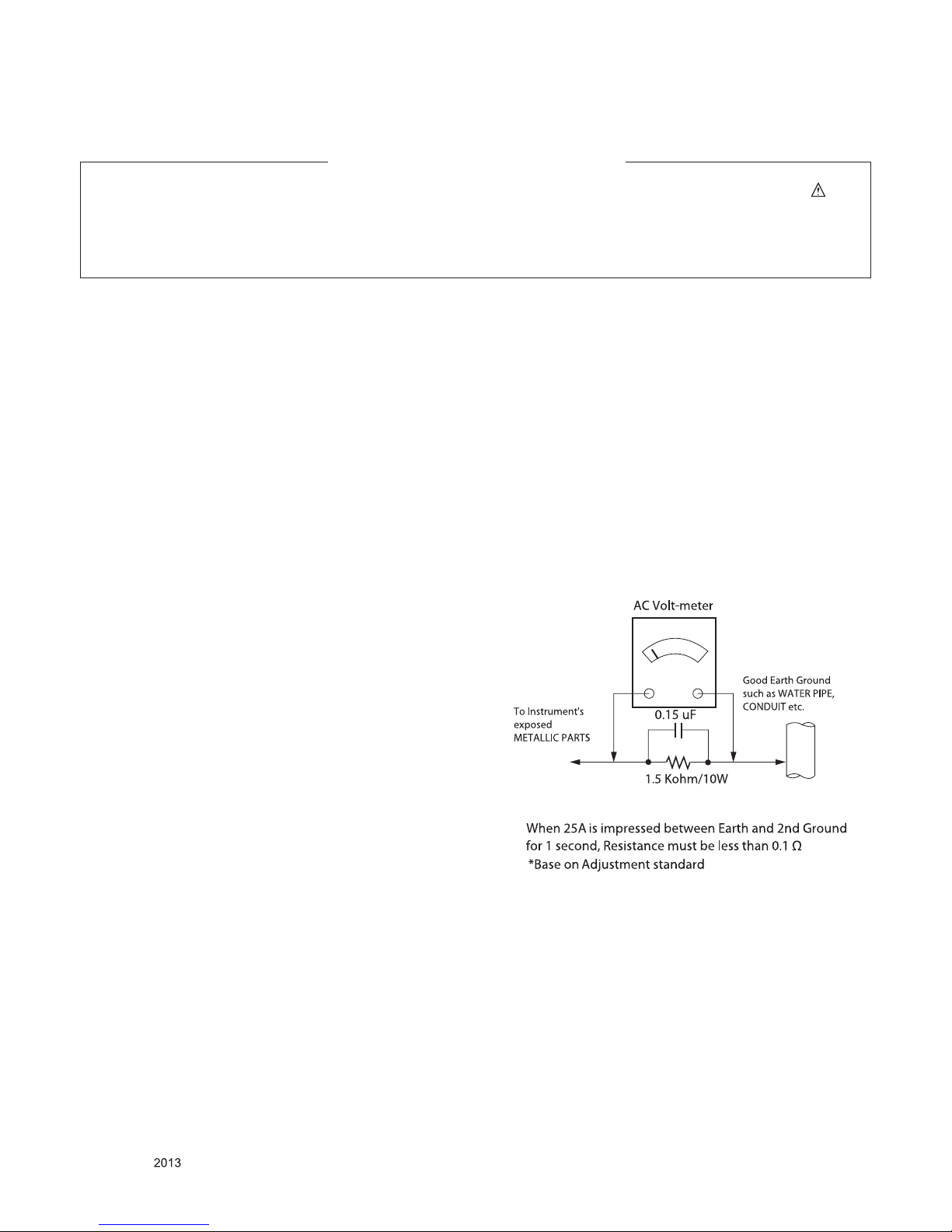
Leakage Current Hot Check (See below Figure)
Plug the AC cord directly into the AC outlet.
Do not use a line Isolation Transformer during this check.
Connect 1.5 K / 10 watt resistor in parallel with a 0.15 uF capacitor
between a known good earth ground (Water Pipe, Conduit, etc.)
and the exposed metallic parts.
Measure the AC voltage across the resistor using AC voltmeter
with 1000 ohms/volt or more sensitivity.
Reverse plug the AC cord into the AC outlet and repeat AC voltage
measurements for each exp ose d metallic par t. Any voltage
measured must not exceed 0.75 volt RMS which is corresponds to
0.5 mA.
In case any measurement is out of the limits specified, there is
possibility of shock hazard and the set must be checked and
repaired before it is returned to the customer.
Leakage Current Hot Check circuit
IMPORTANT SAFETY NOTICE
SAFETY PRECAUTIONS

- 4 -
LGE Internal Use OnlyCopyright © LG Electronics. Inc. All rights reserved.
Only for training and service purposes
SERVICING PRECAUTIONS
CAUTION: Before servicing receivers covered by this service
manual and its supplements and addenda, read and follow the
SAFETY PRECAUTIONS on page 3 of this publication.
NOTE: If unforeseen circumstances create conict between the
following servicing precautions and any of the safety precautions
on page 3 of this publication, always follow the safety precautions. Remember: Safety First.
General Servicing Precautions
1. Always unplug the receiver AC power cord from the AC power
source before;
a. Removing or reinstalling any component, circuit board
module or any other receiver assembly.
b. Disconnecting or reconnecting any receiver electrical plug
or other electrical connection.
c. Connecting a test substitute in parallel with an electrolytic
capacitor in the receiver.
CAUTION: A wrong part substitution or incorrect polarity
installation of electrolytic capacitors may result in an explosion hazard.
2. Test high voltage only by measuring it with an appropriate
high voltage meter or other voltage measuring device (DVM,
FETVOM, etc) equipped with a suitable high voltage probe.
Do not test high voltage by "drawing an arc".
3. Do not spray chemicals on or near this receiver or any of its
assemblies.
4. Unless specied otherwise in this service manual, clean
electrical contacts only by applying the following mixture to the
contacts with a pipe cleaner, cotton-tipped stick or comparable
non-abrasive applicator; 10 % (by volume) Acetone and 90 %
(by volume) isopropyl alcohol (90 % - 99 % strength)
CAUTION: This is a ammable mixture.
Unless specied otherwise in this service manual, lubrication
of contacts in not required.
5. Do not defeat any plug/socket B+ voltage interlocks with which
receivers covered by this service manual might be equipped.
6. Do not apply AC power to this instrument and/or any of its
electrical assemblies unless all solid-state device heat sinks
are correctly installed.
7. Always connect the test receiver ground lead to the receiver
chassis ground before connecting the test receiver positive
lead.
Always remove the test receiver ground lead last.
8. Use with this receiver only the test xtures specied in this
service manual.
CAUTION: Do not connect the test xture ground strap to any
heat sink in this receiver.
Electrostatically Sensitive (ES) Devices
Some semiconductor (solid-state) devices can be damaged easily by static electricity. Such components commonly are called
Electrostatically Sensitive (ES) Devices. Examples of typical ES
devices are integrated circuits and some eld-effect transistors
and semiconductor “chip” components. The following techniques
should be used to help reduce the incidence of component damage caused by static by static electricity.
1. Immediately before handling any semiconductor component or
semiconductor-equipped assembly, drain off any electrostatic
charge on your body by touching a known earth ground. Alternatively, obtain and wear a commercially available discharging wrist strap device, which should be removed to prevent
potential shock reasons prior to applying power to the unit
under test.
2. After removing an electrical assembly equipped with ES
devices, place the assembly on a conductive surface such as
aluminum foil, to prevent electrostatic charge buildup or exposure of the assembly.
3. Use only a grounded-tip soldering iron to solder or unsolder
ES devices.
4. Use only an anti-static type solder removal device. Some solder removal devices not classied as “anti-static” can generate
electrical charges sufcient to damage ES devices.
5. Do not use freon-propelled chemicals. These can generate
electrical charges sufcient to damage ES devices.
6. Do not remove a replacement ES device from its protective
package until immediately before you are ready to install it.
(Most replacement ES devices are packaged with leads electrically shorted together by conductive foam, aluminum foil or
comparable conductive material).
7. Immediately before removing the protective material from the
leads of a replacement ES device, touch the protective material to the chassis or circuit assembly into which the device will
be installed.
CAUTION: Be sure no power is applied to the chassis or circuit, and observe all other safety precautions.
8. Minimize bodily motions when handling unpackaged replacement ES devices. (Otherwise harmless motion such as the
brushing together of your clothes fabric or the lifting of your
foot from a carpeted oor can generate static electricity sufcient to damage an ES device.)
General Soldering Guidelines
1. Use a grounded-tip, low-wattage soldering iron and appropriate tip size and shape that will maintain tip temperature within
the range or 500 °F to 600 °F.
2. Use an appropriate gauge of RMA resin-core solder composed
of 60 parts tin/40 parts lead.
3. Keep the soldering iron tip clean and well tinned.
4. Thoroughly clean the surfaces to be soldered. Use a mall wirebristle (0.5 inch, or 1.25 cm) brush with a metal handle.
Do not use freon-propelled spray-on cleaners.
5. Use the following unsoldering technique
a. Allow the soldering iron tip to reach normal temperature.
(500 °F to 600 °F)
b. Heat the component lead until the solder melts.
c. Quickly draw the melted solder with an anti-static, suction-
type solder removal device or with solder braid.
CAUTION: Work quickly to avoid overheating the circuit
board printed foil.
6. Use the following soldering technique.
a. Allow the soldering iron tip to reach a normal temperature
(500 °F to 600 °F)
b. First, hold the soldering iron tip and solder the strand
against the component lead until the solder melts.
c. Quickly move the soldering iron tip to the junction of the
component lead and the printed circuit foil, and hold it there
only until the solder ows onto and around both the component lead and the foil.
CAUTION: Work quickly to avoid overheating the circuit
board printed foil.
d. Closely inspect the solder area and remove any excess or
splashed solder with a small wire-bristle brush.

- 5 -
LGE Internal Use OnlyCopyright © LG Electronics. Inc. All rights reserved.
Only for training and service purposes
IC Remove/Replacement
Some chassis circuit boards have slotted holes (oblong) through
which the IC leads are inserted and then bent at against the circuit foil. When holes are the slotted type, the following technique
should be used to remove and replace the IC. When working with
boards using the familiar round hole, use the standard technique
as outlined in paragraphs 5 and 6 above.
Removal
1. Desolder and straighten each IC lead in one operation by
gently prying up on the lead with the soldering iron tip as the
solder melts.
2. Draw away the melted solder with an anti-static suction-type
solder removal device (or with solder braid) before removing
the IC.
Replacement
1. Carefully insert the replacement IC in the circuit board.
2. Carefully bend each IC lead against the circuit foil pad and
solder it.
3. Clean the soldered areas with a small wire-bristle brush.
(It is not necessary to reapply acrylic coating to the areas).
"Small-Signal" Discrete Transistor
Removal/Replacement
1. Remove the defective transistor by clipping its leads as close
as possible to the component body.
2. Bend into a "U" shape the end of each of three leads remaining on the circuit board.
3. Bend into a "U" shape the replacement transistor leads.
4. Connect the replacement transistor leads to the corresponding
leads extending from the circuit board and crimp the "U" with
long nose pliers to insure metal to metal contact then solder
each connection.
Power Output, Transistor Device
Removal/Replacement
1. Heat and remove all solder from around the transistor leads.
2. Remove the heat sink mounting screw (if so equipped).
3. Carefully remove the transistor from the heat sink of the circuit
board.
4. Insert new transistor in the circuit board.
5. Solder each transistor lead, and clip off excess lead.
6. Replace heat sink.
Diode Removal/Replacement
1. Remove defective diode by clipping its leads as close as possible to diode body.
2. Bend the two remaining leads perpendicular y to the circuit
board.
3. Observing diode polarity, wrap each lead of the new diode
around the corresponding lead on the circuit board.
4. Securely crimp each connection and solder it.
5. Inspect (on the circuit board copper side) the solder joints of
the two "original" leads. If they are not shiny, reheat them and
if necessary, apply additional solder.
Fuse and Conventional Resistor
Removal/Replacement
1. Clip each fuse or resistor lead at top of the circuit board hollow
stake.
2. Securely crimp the leads of replacement component around
notch at stake top.
3. Solder the connections.
CAUTION: Maintain original spacing between the replaced
component and adjacent components and the circuit board to
prevent excessive component temperatures.
Circuit Board Foil Repair
Excessive heat applied to the copper foil of any printed circuit
board will weaken the adhesive that bonds the foil to the circuit
board causing the foil to separate from or "lift-off" the board. The
following guidelines and procedures should be followed whenever this condition is encountered.
At IC Connections
To repair a defective copper pattern at IC connections use the
following procedure to install a jumper wire on the copper pattern
side of the circuit board. (Use this technique only on IC connections).
1. Carefully remove the damaged copper pattern with a sharp
knife. (Remove only as much copper as absolutely necessary).
2. carefully scratch away the solder resist and acrylic coating (if
used) from the end of the remaining copper pattern.
3. Bend a small "U" in one end of a small gauge jumper wire and
carefully crimp it around the IC pin. Solder the IC connection.
4. Route the jumper wire along the path of the out-away copper
pattern and let it overlap the previously scraped end of the
good copper pattern. Solder the overlapped area and clip off
any excess jumper wire.
At Other Connections
Use the following technique to repair the defective copper pattern
at connections other than IC Pins. This technique involves the
installation of a jumper wire on the component side of the circuit
board.
1. Remove the defective copper pattern with a sharp knife.
Remove at least 1/4 inch of copper, to ensure that a hazardous
condition will not exist if the jumper wire opens.
2. Trace along the copper pattern from both sides of the pattern
break and locate the nearest component that is directly connected to the affected copper pattern.
3. Connect insulated 20-gauge jumper wire from the lead of the
nearest component on one side of the pattern break to the
lead of the nearest component on the other side.
Carefully crimp and solder the connections.
CAUTION: Be sure the insulated jumper wire is dressed so the
it does not touch components or sharp edges.
- 6 -
LGE Internal Use OnlyCopyright © LG Electronics. Inc. All rights reserved.
Only for training and service purposes
SPECIFICATION
NOTE : Specifications and others are subject to change without notice for improvement
.
1. Application range
This specification is applied to the LED TV used LB43B
chassis.
2. Requirement for Test
Each part is tested as below without special appointment.
1) Temperature: 25 °C ± 5 °C(77 °F ± 9 °F), CST: 40 °C ± 5 °C
2) Relative Humidity: 65 % ± 10 %
3) Power Voltage
: Standard input voltage (AC 100-240 V~, 50/60 Hz)
* Standard Voltage of each products is marked by models.
4) Specification and performance of each parts are followed
ea ch drawing and s pe cificatio n b y p art number in
accordance with BOM.
5) The receiver must be operated for about5 minutes prior to
the adjustment.
3. Test method
1) Performance: LGE TV test method followed
2) Demanded other specification
- Safety : CE, IEC specification
- EMC : CE, IEC
4. Model General Specification
No. Item Specication Remarks
1. Market
Asia, Oceania, Africa, Middle East
(PAL/DVB Market)
2. Broadcasting system
1) PAL/SECAM-B/G/D/K/I
2) NTSC-M
3) DVB-T/T2
► DTV
LB43B/LB43M support DVB-T
LB43T support DVB-T//T2
3. Channel Storage ATV - 135EA, DTV - 1000EA
4. Receiving system
Analog : Upper Heterodyne
Digital : COFDM(DVB-T)
► DVB-T
- Guard Interval (Bitrate_Mbit/s)
1/4, 1/8, 1/16, 1/32
- Modulation : Code Rate
QPSK : 1/2, 2/3, 3/4, 5/6, 7/8
16-QAM : 1/2, 2/3, 3/4, 5/6, 7/8
64-QAM : 1/2, 2/3, 3/4, 5/6, 7/8
► DVB-T2
- Guard Interval (Bitrate_Mbit/s)
1/4, 1/8, 1/16, 1/32, 1/128, 19/128, 19/256,
- Modulation : Code Rate
QPSK : 1/2, 2/5, 2/3, 3/4, 5/6
16-QAM : 1/2, 2/5, 2/3, 3/4, 5/6
64-QAM : 1/2, 2/5, 2/3, 3/4, 5/6
256-QAM : 1/2, 2/5, 2/3, 3/4, 5/6
5. Video(Composite Input) PAL, SECAM, NTSC 4 System : PAL, SECAM, NTSC, PAL60
6. Component Input Y/Cb/Cr, Y/Pb/Pr
7. HDMI Input
HDMI1-DTV/DVI
HDMI2-DTV/MHL
Support HDCP
8. SPDIF out SPDIF out Except 32”HD model
9. USB Input For My Media(Movie/Photo/Music List) and SVC
10. Headphone
- 7 -
LGE Internal Use OnlyCopyright © LG Electronics. Inc. All rights reserved.
Only for training and service purposes
5. Component Video Input (Y,
Cb/Pb, Cr/Pr)
No. Resolution H-freq(kHz) V-freq(Hz) Porposed
1 720×480 15.73 60.00 SDTV, DVD 480i
2 720×480 15.63 59.94 SDTV, DVD 480i
3 720×480 31.47 59.94 480p
4 720×480 31.50 60.00 480p
5 720×576 15.625 50.00 SDTV, DVD 625 Line
6 720×576 31.25 50.00 HDTV 576p
7 1280×720 45.00 50.00 HDTV 720p
8 1280×720 44.96 59.94 HDTV 720p
9 1280×720 45.00 60.00 HDTV 720p
10 1920×1080 31.25 50.00 HDTV 1080i
11 1920×1080 33.75 60.00 HDTV 1080i
12 1920×1080 33.72 59.94 HDTV 1080i
13 1920×1080 56.250 50 HDTV 1080p
14 1920×1080 67.5 60 HDTV 1080p
6. HDMI Input : Refer to adjust specification about EDID data.
6.1. DTV mode
No. Resolution H-freq(kHz) V-freq.(kHz) Pixel clock(MHz) Proposed
1. 720*480 31.469 / 31.5 59.94 / 60 27.00/27.03 SDTV 480P
2. 720*576 31.25 50 54 SDTV 576P
3. 1280*720 37.500 50 74.25 HDTV 720P
4. 1280*720 44.96 / 45 59.94 / 60 74.17/74.25 HDTV 720P
5. 1920*1080 33.72 / 33.75 59.94 / 60 74.17/74.25 HDTV 1080I
6. 1920*1080 28.125 50.00 74.25 HDTV 1080I
7. 1920*1080 26.97 / 27 23.97 / 24 74.17/74.25 HDTV 1080P
8. 1920*1080 33.716/33.75 29.976/30.00 74.25 HDTV 1080P
9. 1920*1080 56.250 50 148.5 HDTV 1080P
10. 1920*1080 67.43 / 67.5 59.94 / 60 148.35/148.50 HDTV 1080P
6.2. PC mode
No. Resolution H-freq(kHz) V-freq.(Hz) Pixel clock(MHz) Proposed Remark
1. 640*350 @70Hz 31.468 70.09 25.17 EGA
2. 720*400 @70Hz 31.469 70.08 28.321 DOS
3. 640*480 @60Hz 31.469 59.940 25.175 VESA(VGA)
4. 800*600 @60Hz 37.879 60.31 40.000 VESA(SVGA)
5. 1024*768 @60Hz 48.363 60.00 65.000 VESA(XGA)
6 1152*864 @60Hz 54.348 60.053 80.002 VESA
7. 1280*1024 @60Hz 63.981 60.020 108 VESA(SXGA) FHD only(Support to HDMI-PC)
8. 1360*768 @60Hz 47.712 60.015 85.5 VESA(WXGA)
9. 1920*1080 @60Hz 67.5 60.0 148.5
WUXGA
(Reduced blanking)
FHD only(Support to HDMI-PC)
- 8 -
LGE Internal Use OnlyCopyright © LG Electronics. Inc. All rights reserved.
Only for training and service purposes
ADJUSTMENT INSTRUCTION
1. Application Range
This specification sheet is applied to all of the LED TV with
LB43B chassis.
2. Designation
(1) Th e ad justm ent is accord ing to the order whic h is
designated and which must be followed, according to the
plan which can be changed only on agreeing.
(2) Power adjustment : Free Voltage.
(3) Magnetic Field Condition: Nil.
(4) Input signal Unit: Product Specification Standard.
(5) Reserve after operation: Above 5 Minutes (Heat Run)
Temperature : at 25 °C ± 5 °C
Relative humidity : 65 ± 10 %
Input voltage : 100-220 V~, 50/60 Hz
(6) Adjustment equipments
: Color Analyzer(CA-210 or CA-110), Service remote control.
(7) Push the “IN STOP" key - For memory initialization.
3. Main PCB check process
▪ APC - After Manual-Insert, executing APC
* Boot file Download
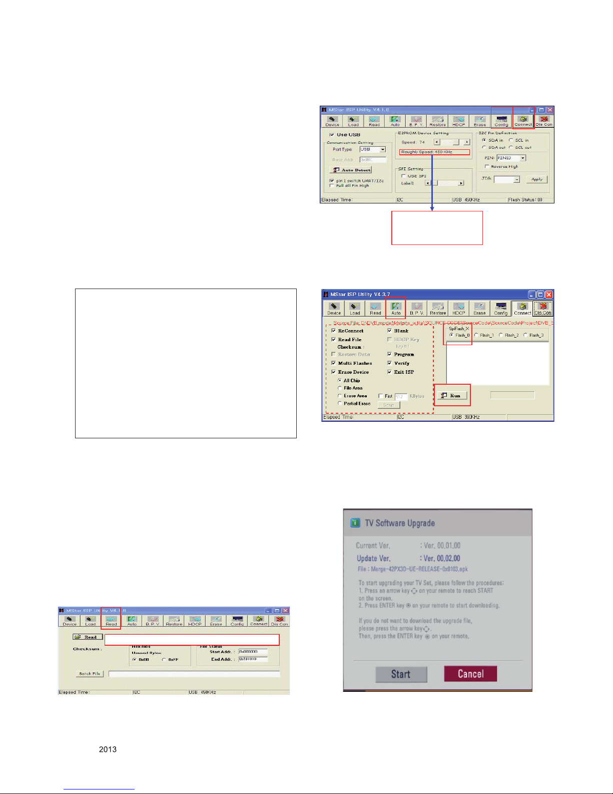
(1) Execute ISP program "Mstar ISP Utility" and then click
"Config" tab.
(2) Set as below, and then click "Auto Detect" and check "OK"
message.
If "Error" is displayed, check connection between computer,
jig, and set.
(3) Click "Read" tab, and then load download file(XXXX.bin)
by clicking "Read"
(4) Click "Connect" tab. If "Can't" is displayed, check connection
between computer, jig and set.
(5) Click "Auto" tab and set as below.
(6) Click "Run".
(7) After downloading, check "OK" message.
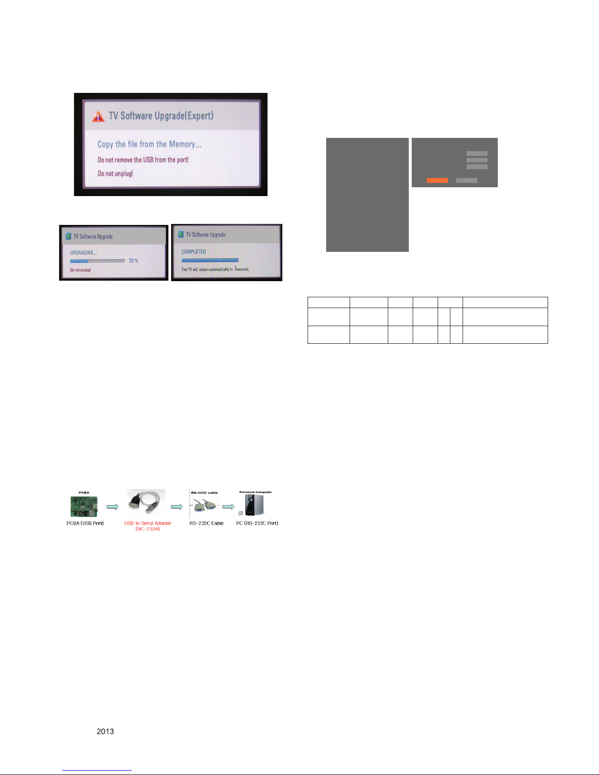
* USB DOWNLOAD(*.epk file download)
(1) Put the USB Stick to the USB socket.
(2) Automatically detecting update file in USB Stick.
- If version of update file in USB Stick is lower, it will not
work. But version of update file is higher, USB data will be
detected automatically.
Case1 : Software version up
1. After downloading S/W by USB , TV set will reboot
automatically.
2. Push “In-stop” key.
3. Push “Power on” key.
4. Function inspection
5. After function inspection, Push “In-stop” key.
Case2 : Function check at the assembly line
1. When TV set is entering on the assembly line, Push
“In-stop” key at rst.
2. Push “Power on” key for turning it on.
→ If you push “Power on” key, TV set will recover
channel information by itself.
3. After function inspection, Push “In-stop” key.
(1)
filexxx.bin
(4)
(5)
(6)
(7)...........OK
filexxx.bin
(2)
(3)
Please Check the Speed :
To use speed between
from 200KHz to 400KHz
- 9 -
LGE Internal Use OnlyCopyright © LG Electronics. Inc. All rights reserved.
Only for training and service purposes
(3) Show the message "Copying files from memory".
(4) Updating is starting.
(5) Updating Completed, The TV will restart automatically.
(6) If your TV is turned on, check your updated version and
Tool option. (explain the Tool option, next stage)
* If updated version is higher than what TV has, the TV can
lost all channel data. In this case, you have to channel
recover. If all channel data is cleared, you didn’t have a
DTV/ATV test on production line.
* After downloading, have to adjust Tool Option again.
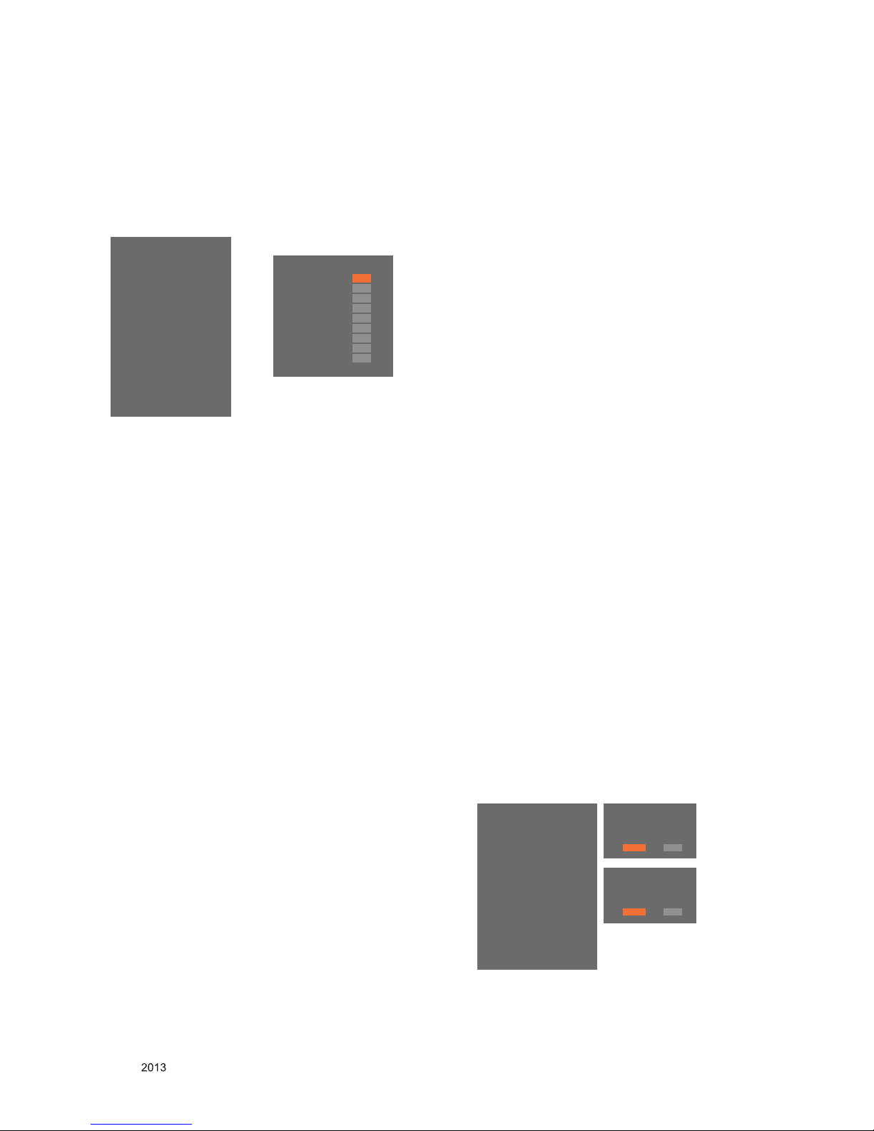
(1) Push "IN-START" key in service remote control.
(2) Select "Tool Option 1" and push "OK" key.
(3) Punch in the number. (Each model has their number)
(4) Completed selecting Tool option.
*
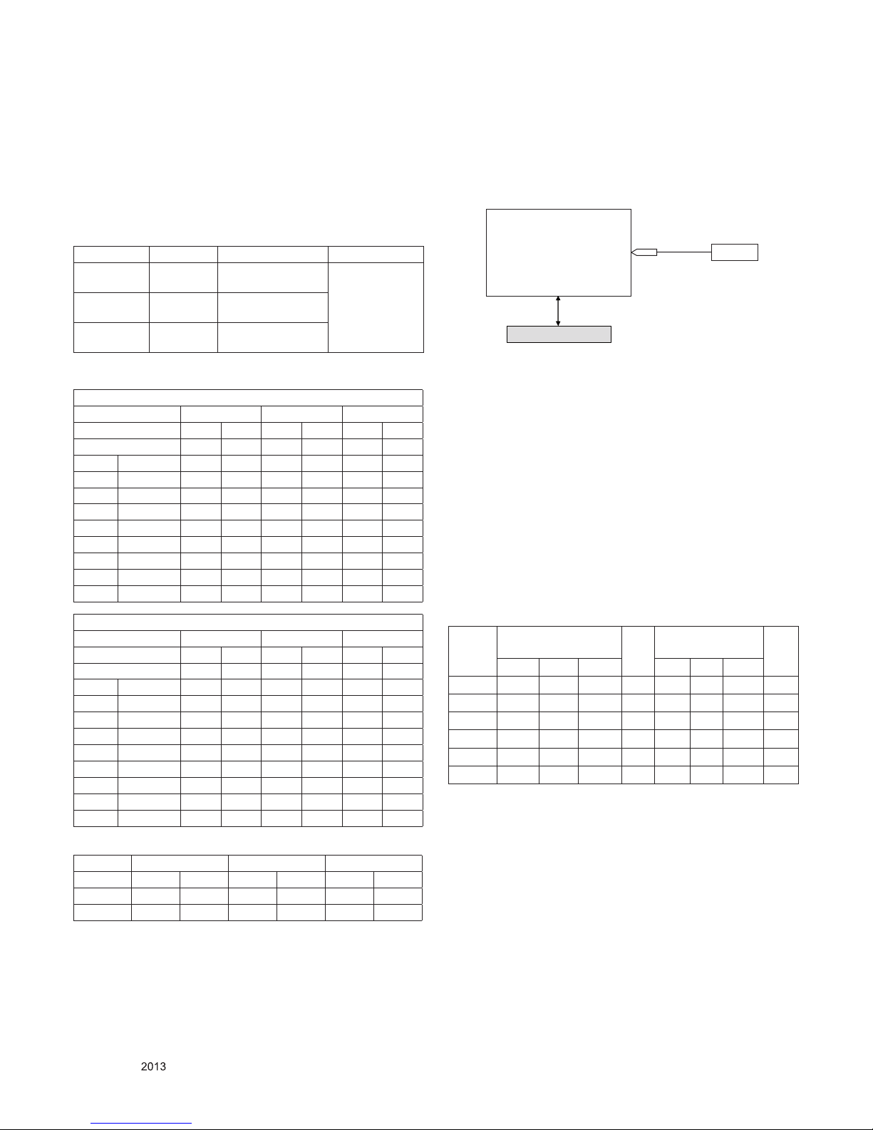
RS-232C Connection Method.
Connection : PCBA (USB Port) → USB to Serial Adapter
(UC-232A) → RS-232C cable → PC(RS-232C port)
● Product name of USB to Serial Adapter is UC-232A.
4. ADC Process
4.1. ADC
- Enter Service Mode by pushing "ADJ" key,
- Enter Internal ADC mode by pushing "►" key at "8. ADC
Calibration".
<Caution> Using "P-ONLY" key of the Adjustment remote
control, power on TV.
* ADC Calibration Protocol (RS232)
Adjust Sequence
▪ aa 00 00 [Enter Adjust Mode]
▪ xb 00 40 [Component1 Input (480i)]
▪ ad 00 10 [Adjust 480i Comp1]
▪ aa 00 90 End Adjust mode
* Required equipment : Adjustment remote control.
4.2. Function Check
4.2.1. Check display and sound
■ Check Input and Signal items.
(1) TV
(2) AV (CVBS)
(3) COMPONENT (480i)
(4) HDMI
* Display and Sound check is executed by Remote control.
<Caution> Not to push the "INSTOP" key after completion if
the function inspection.
NO Item CMD 1 CMD 2 Data 0
Enter
Adjust MODE
Adjust
‘Mode In’
A A 0 0
When transfer the ‘Mode In’,
Carry the command.
ADC adjust ADC Adjust A D 1 0
Automatically adjustment
(The use of a internal pattern)
EZ ADJUST
0. Tool Option1
1. Tool Option2
2. Tool Option3
3. Tool Option4
4. Tool Option5
5. Tool Option Commercial
6. Country Group
7. Area Option
8. ADC Calibration ►
9. White Balance
10. 10 Point WB
11. Test Pattern
12. EDID D/L
13. Sub B/C
14. Ext. Input Adjust
ADC Calibration
ADC Comp 480i
ADC Comp 1080p
ADC Type ◄ ►
Start
NG
NG
OPT
Reset
- 10 -
LGE Internal Use OnlyCopyright © LG Electronics. Inc. All rights reserved.
Only for training and service purposes
5. Total Assembly line process
5.1. Adjustment Preparation
▪ W/B Equipment condition
CA210: CH14, Test signal: Inner pattern(80IRE)-LED Module
▪ Above 5 minutes H/run in the inner pattern. ("power on" key
of Adjustment remote control)
* The spec of color temperature and coordinate.
* W/B Table in process of aging time
- LGD Module
- AUO/COST/SHARP/BOE Module which cool spec is 13000 K
* Connecting picture of the measuring instrument
(On Automatic control)
Inside Pattern is used when W/B is controlled. Connect to
auto controller or push Adjustment Remote control POWER
ON → Enter the mode of White-Balance, the pattern will
come out.
* Auto-control interface and directions
(1) Adjust in the place where the influx of light like floodlight
around is blocked. (Illumination is less than 10 lux).
(2) Adhere closely the Color analyzer(CA210) to the module
less than 10 cm distance, keep it with the surface of the
Module and Color analyzer's prove vertically.(80° ~ 100°).
(3) Aging time
- After aging start, keep the power on (no suspension of
power supply) and heat-run over 5 minutes.
- Using ‘no signal’ or ‘full white pattern’ or the others,
check the back light on.
▪ Auto adjustment Map(RS-232C)
RS-232C COMMAND
[CMD ID DATA]
Wb 00 00 White Balance Start
Wb 00 ff White Balance End
<Caution>
Color Temperature : COOL, Medium, Warm.
One of R Gain/G Gain/ B Gain should be kept on 0xC0, and
adjust other two lower than C0.(When R/G/B Gain are all
C0, it is the FULL Dynamic Range of Module)
Full White Pattern
CA-210
COLOR
ANALYZER
TYPE : CA-210
RS-232C Communication
Mode Color Temp Color coordinate Remark
Cool (C50) 13,000 K
X=0.271 (±0.002)
Y=0.270 (±0.002)
<Test Signal>
- Inner pattern
for W/B adjust
- External white
pattern
(80IRE, 204gray)
Medium(0) 9,300 K
X=0.286 (±0.002)
Y=0.289 (±0.002)
Warm(W50) 6,500 K
X=0.313 (±0.002)
Y=0.329 (±0.002)
(normal line) March ~ December
Aging time(Min) Cool Medium Warm
color coordinate X y x y x y
Target 271 270 286 289 313 329
1 0-2 282 289 297 308 324 348
2 3-5 281 287 296 306 323 346
3 6-9 279 284 294 303 321 343
4 10-19 277 280 292 299 319 339
5 20-35 275 277 290 296 317 336
6 36-49 274 274 289 293 316 333
7 50-79 273 272 288 291 315 331
8 80-119 272 271 287 290 314 330
9 Over 120 271 270 286 289 313 329
(normal line) January ~ Feburary
Aging time Cool Medium Warm
color coordinate x y x y x y
Target 271 270 286 289 313 329
1 0-2 286 295 301 314 328 354
2 3-5 284 290 299 309 326 349
3 6-9 282 287 297 306 324 346
4 10-19 279 283 294 302 321 342
5 20-35 276 278 291 297 318 337
6 36-49 274 275 289 294 316 334
7 50-79 273 272 288 291 315 331
8 80-119 272 271 287 290 314 330
9 Over 120 271 270 286 289 313 329
Cool Medium Warm
x y x y x y
spec 271 270 285 293 313 329
target 276 277 290 300 318 336
RS-232C COMMAND
[CMD ID DATA]
MIN
CENTER
(DEFAULT)
MAX
Cool Mid Warm Cool Mid Warm
R Gain jg Ja jd 00 172 192 192 192
G Gain jh Jb je 00 172 192 192 192
B Gain ji Jc jf 00 192 192 172 192
R Cut 64 64 64 128
G Cut 64 64 64 128
B Cut 64 64 64 128
- 11 -
LGE Internal Use OnlyCopyright © LG Electronics. Inc. All rights reserved.
Only for training and service purposes
* Manual W/B process using adjust Remote control.
■ Color analyzer(CA100+, CA210) should be used in the
calibrated ch by CS-1000.
■ Operate the zero-calibration of the CA100+ or CA-210,
then stick sensor to the module when adjusting.
■ After enter Service Mode by pushing “ADJ” key,
■ Enter White Balance by pushing “►” key at “9. White
Balance”.
■ For manual adjustment, it is also possible by the following
sequence.
(1) Set TV in Adj. mode using “P-ONLY” key on remote
controller and then operate heat run longer than 15
minutes.(If not executed this step, the condition for W/B
may be different.)
(2) Push “Exit” key.
(3) Enter White Balance mode by pushing the ADJ key and
select “9. White Balance”. When KEY (►) is pressed,
206 Gray internal pattern will be displayed.
(4) Zero Calibrate the probe of Color Analyzer, then place it
on the center of LCD module within 10cm of the surface
(5) Sele ct eac h it ems (R ed/Gr een/Blu e Ga in) us ing
▲/▼(CH +/-) key on Remote control.
(6) Adjust R/ G/ B Gain using ◄/►(VOL +/-) key on R/C.
(7) Adjust three modes all (Cool / Medium / Warm)
- For All model w/o LS345
Fix the one of R/G/B gain and change the others
- For G-FIX model
Cool Mode
1) Fix the one of R/G/B gain to 192 (default data) and
decrease the others. (If G gain is adjusted over 172
and R and B gain less than 192 , Adjust is O.K.)
2) If G gain is less than 172, Increase G gain by up to
172, and then increase R gain and G gain same
amount of increasing G gain.
3) If R gain or B gain is over 255, readjust G gain less
than 172, Conform to R gain is 255 or B gain is 255
Medium / Warm Mode - Fix the one of R/G/B gain
to 192 (default data) and decrease the others.
(8) When adjustment is completed, exit adjustment mode
using EXIT key on Remote control.
* CASE Cool
First adjust the coordinate far away from the target
value(x, y).
1) x, y > target
i) Decrease the R, G.
2) x, y < target
i) First decrease the B gain,
ii) Decrease the one of the others.
3) x > target, y < target
i) First decrease B, so make y a little more than the
target.
ii) Adjust x value by decreasing the R.
4) x < target, y > target
i) First decrease B, so make x a little more than the
target.
ii) Adjust x value by decreasing the G.
* After You finish all adjustments, Press “In-start” button
and compare Tool option and Area option value with its
BOM, if it is correctly same then unplug the AC cable.
If it is not same, then correct it same with BOM and
unplug AC cable.
For correct it to the model’s module from factory JIG
model.
* Push the “IN STOP" key after completing the function
inspection.
5.2. DDC EDID Write (HDMI 256Byte)
■ Connect HDMI Signal Cable to HDMI Jack.
■ Write EDID DATA to EEPROM(24C02) by using DDC2B
protocol.
■ Check whether written EDID data is correct or not.
* For SVC main Assembly, EDID have to be downloaded to
Insert Process in advance.
5.3. EDID DATA
1) All Data : HEXA Value
2) Changeable Data :
*: Serial No : Controlled / Data:01
**: Month : Controlled / Data:00
***: Year : Controlled
****: Check sum
- Auto Download
■ After enter Service Mode by pushing “ADJ” key,
■ Enter EDID D/L mode.
■ Enter “START” by pushing “OK” key.
EZ ADJUST
0. Tool Option1
1. Tool Option2
2. Tool Option3
3. Tool Option4
4. Tool Option5
5. Tool Option Commercial
6. Country Group
7. Area Option
8. ADC Calibration
9. White Balance
10. 10 Point WB
11. Test Pattern
12 EDID D/L
13. Sub B/C
14. Ext. Input Adjust
Whit Balance
Color Temp. ◄ ►
R-Gain
G-Gain
B-Gain
R-Cut
G-Cut
B-Cut
Test-Pattern
Backlight
Reset To Set
Cool
172
192
192
64
64
64
ON
100
EZ ADJUST
0. Tool Option1
1. Tool Option2
2. Tool Option3
3. Tool Option4
4. Tool Option5
5. Tool Option Commercial
6. Country Group
7. Area Option
8. ADC Calibration
9. White Balance
10. 10 Point WB
11. Test Pattern
12. EDID D/L ►
13. Sub B/C
14. Ext. Input Adjust
EDID D/L
HDMI1 NG
HDMI2 NG
Start
Reset
EDID D/L
HDMI1 OK
HDMI2 OK
Start
Reset
- 12 -
LGE Internal Use OnlyCopyright © LG Electronics. Inc. All rights reserved.
Only for training and service purposes
[Caution]
* Use the proper signal cable for EDID Download
- Analog EDID : Pin3 exists
- Digital EDID : Pin3 exists
* Edid data and Model option download (RS232)
(1) FHD 8BIT 2D HDMI EDID DATA
(2) Detail EDID Options are below
a. Product ID
b. Serial No: Controlled on production line.
c. Month, Year: Controlled on production line:
ex) Week : '01' -> '01'
Year : '2012' -> '16' fix
d. Model Name(Hex):
cf) TV set’s model name in EDID data is below.
e. Checksum: Changeable by total EDID data.
f. Vendor Specific
- FHD 8bit Model
5.4. Outgoing condition Configuration
■ When pressing IN-STOP key by Service remote control,
Red LED are blinked alternatively. And then automatically
turn off. (Must not AC power OFF during blinking)
5.5. GND and HI-POT Test
5.5.1. GND & HI-POT auto-check preparation
(1) Check the POWER CABLE and SIGNAL CABE insertion
condition.
(2) You can’t use Tuner Ground & Tuner signal line at all
models (applied Isolator inner tuner)
5.5.2. GND & HI-POT auto-check
(1) Pallet moves in the station.(POWER CORD / AV CORD is
tightly inserted)
(2) Connect the AV JACK Tester.
(3) Controller (GWS103-4) on.
(4) GND Test (Auto)
- If Test is failed, Buzzer operates.
- If Test is passed, execute next process(Hi-pot test).
(Remove A/V CORD from A/V JACK BOX)
(5) HI-POT test (Auto)
- If Test is failed, Buzzer operates.
- If Test is passed, GOOD Lamp on and move to next
process automatically.
5.5.3. Checkpoint
(1) Test voltage
1) 3 Poles
- GND: 1.5KV/min at 100 mA
- SIGNAL: 3KV/min at 100 mA
2) 2 Poles
- SIGNAL: 3 KV/min at 100 mA
(2) TEST time: 1 second
(3) TEST POINT
1) 3 Poles
- GND Test = POWER CORD GND and SIGNAL
CABLE GND.
- Hi-pot Test = POWER CORD GND and LIVE &
NEUTRAL.
2) 2 Poles
- Hi-pot Test = Accessible Metal and LIVE & NEUTRAL.
(4) LEAKAGE CURRENT: At 0.5mArms
NO Item CMD 1 CMD 2 Data 0
Enter download
Mode
Download
‘Mode In’
A A 0 0
When transfer the ‘Mode In’,
Carry the command.
EDID data and
Model option
download
ADC Adjust A E 00 10
Automatically adjustment
(The use of a internal pattern)
No. Item Condition Hex Data
1 Manufacturer ID GSM 1E6D
2 Version Digital : 1 01
3 Revision Digital : 3 03
0 1 2 3 4 5 6 7 8 9 A B C D E F
0 00 FF FF FF FF FF FF 00 1E 6D A B
10 C 01 03 80 A0 5a 78 0A EE 91 A3 54 4C 99 26
20 0F 50 54 A1 08 00 31 40 45 40 61 40 71 40 81 8 0
30 01 01 01 01 01 01 02 3A 80 18 71 38 2D 40 58 2C
40 45 00 A0 5A 00 00 00 1E 66 21 50 B0 51 00 1B 30
50 40 70 36 00 A0 5A 00 00 0 0 1E 00 0 0 0 0 FD 00 3A
60 3E 1E 53 10 00 0A 20 20 20 20 20 20 D
70 D 01 E
80 02 03 22 F1 4E 10 9F 04 13 05 14 03 02 12 20 21
90 22 15 01 26 15 07 50 09 57 07 f
A0 80 1E 01 1d 80 18 71 1c 16 20 58 2c 25 00 20 C2
B0 31 00 0 9e 01 1d 00 72 51 d0 1e 20 6e 28 55 00
C0 20 C2 31 00 00 1e 02 3a 80 18 71 38 2d 40 58 2c
D0 45 00 A0 5a 00 00 00 1e 01 1d 00 Bc 52 d0 1e 20
E0 B8 28 55 40 C4 8e 21 00 00 1e 00 00 00 00 00 00
F0 00 00 00 00 00 00 00 00 00 00 00 00 00 00 00 E
Model Name HEX EDID Table DDC Function
HD/FHD Model 0001 01 00 Analog/Digital
MODEL NAME MODEL NAME(HEX)
LG TV 00 00 00 FC 00 4C 47 20 54 56 0A 20 20 20 20 20 20 20 (LG TV)
EDID C/S data
FHD-8BIT
HDMI
Check Sum
(Hex)
Block 0 41
Block 1
25 (HDMI1)
15 (HDMI2)
Input Model name(HEX)
HDMI1 67030C001000
HDMI2 67030C002000
- 13 -
LGE Internal Use OnlyCopyright © LG Electronics. Inc. All rights reserved.
Only for training and service purposes
6. 3D function test
(Pattern Generator MSHG-600, MSPG-6100[Support HDMI1.4])
* HDMI mode No. 872 , pattern No.83
(1) Please input 3D test pattern like below.
(2) When 3D OSD appear automatically, then select OK button.
(3) Don't wear a 3D Glasses, check the picture like below.
- 14 -
LGE Internal Use OnlyCopyright © LG Electronics. Inc. All rights reserved.
Only for training and service purposes
900
200
400
410
540
521
530
820
501
500
120
310
121
LV1
A2
A10
Set + Stand
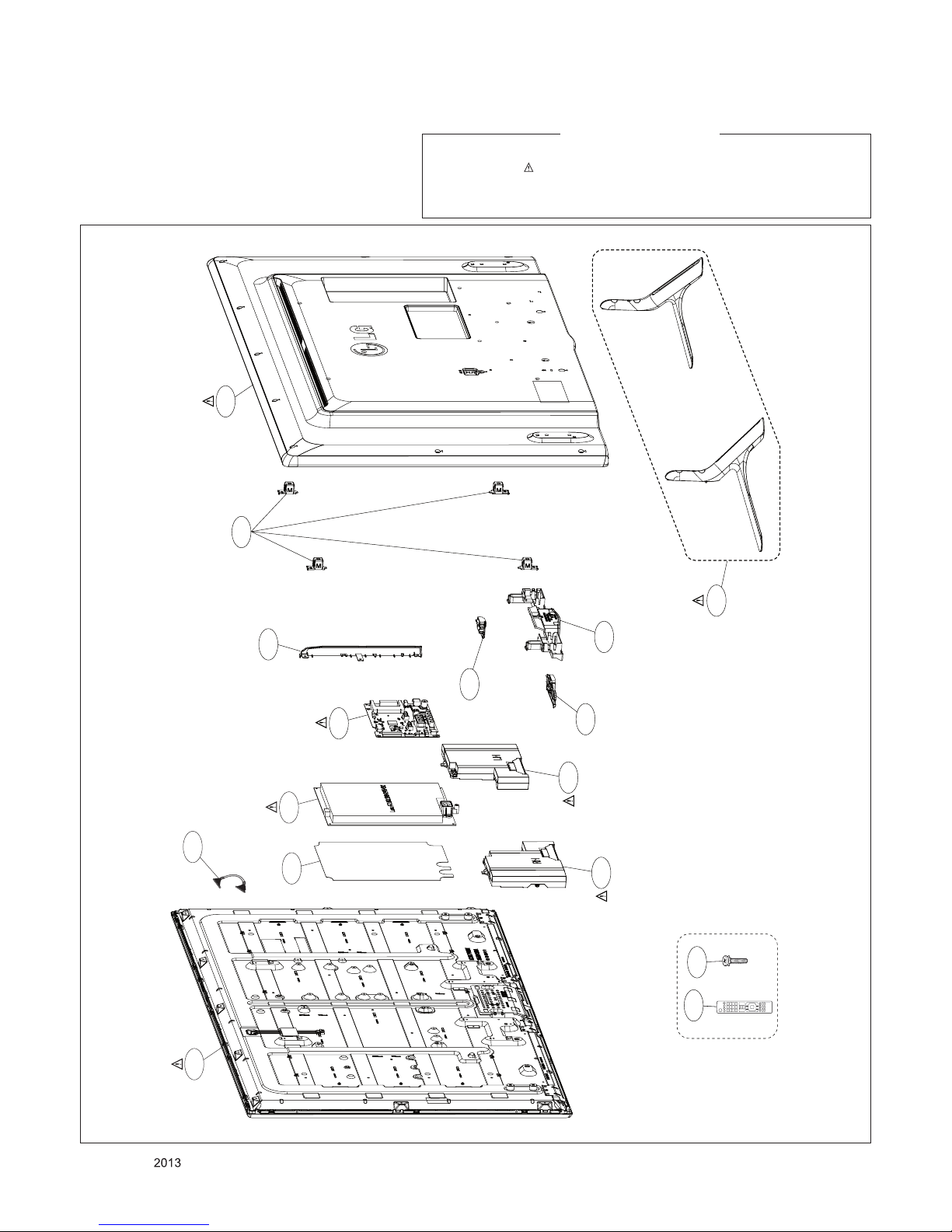
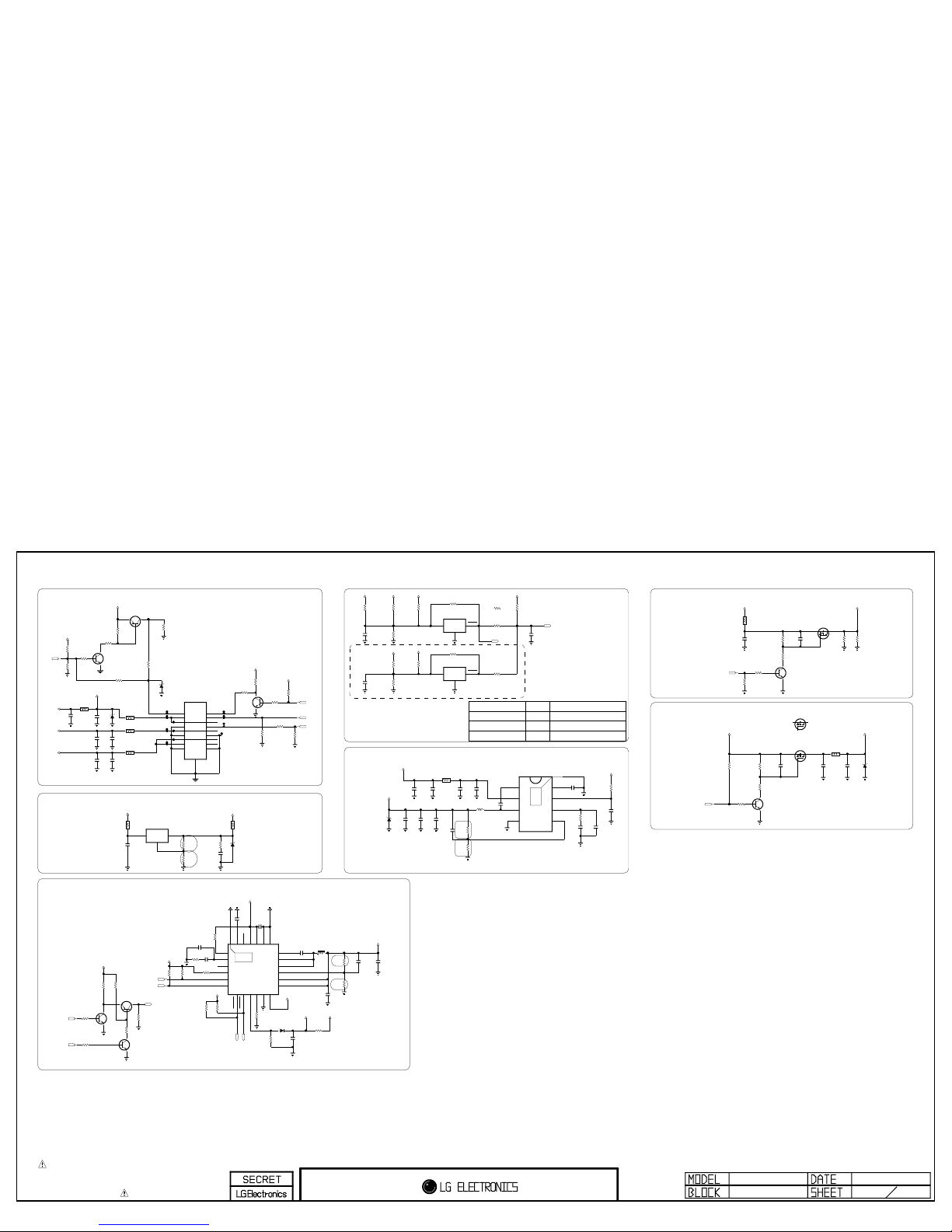
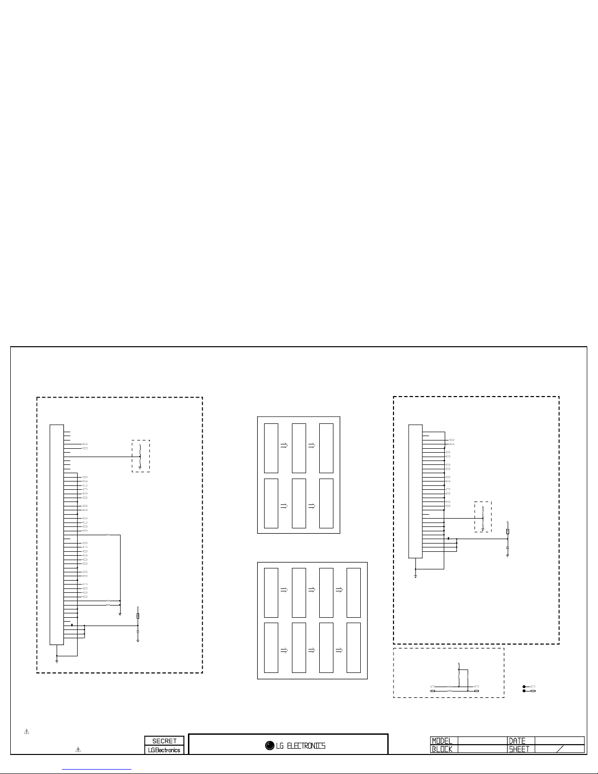
EXPLODED VIEW
Many electrical and mechanical parts in this chassis have special safety-related characteristics. These
parts are identified by in the Schematic Diagram and EXPLODED VIEW.
It is essenti al that these special safet y parts shoul d be replac ed with the same compo nents as
recommended in this manual to prevent X-RADIATION, Shock, Fire, or other Hazards.
Do not modify the original design without permission of manufacturer.
IMPORTANT SAFETY NOTICE
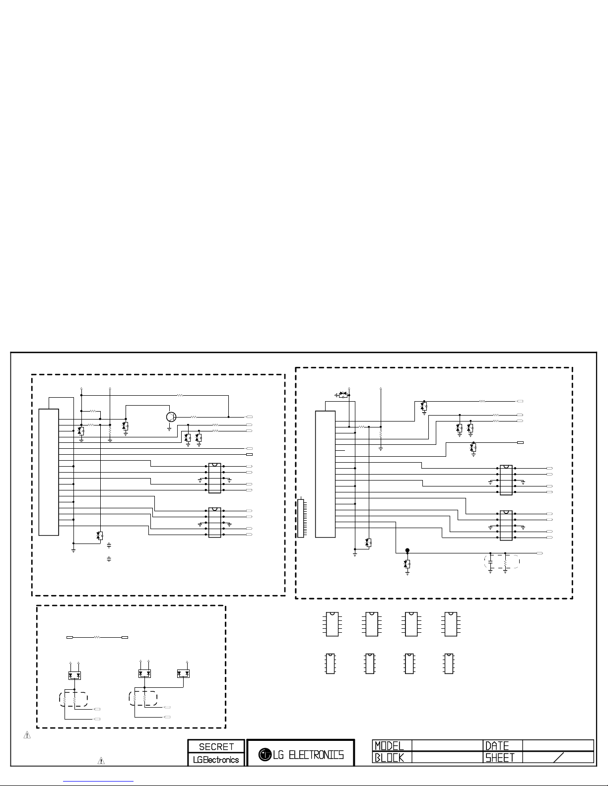
THE SYMBOL MARK OF THIS SCHEMETIC DIAGRAM INCORPORATES
SPECIAL FEATURES IMPORTANT FOR PROTECTION FROM X-RADIATION.
FIRE AND ELECTRICAL SHOCK HAZARDS, WHEN SERVICING IF IS
ESSENTIAL THAT ONLY MANUFACTURES SPECIFIED PARTS BE USED FOR
THE CRITICAL COMPONENTS IN THE SYMBOL MARK OF THE SCHEMETIC.
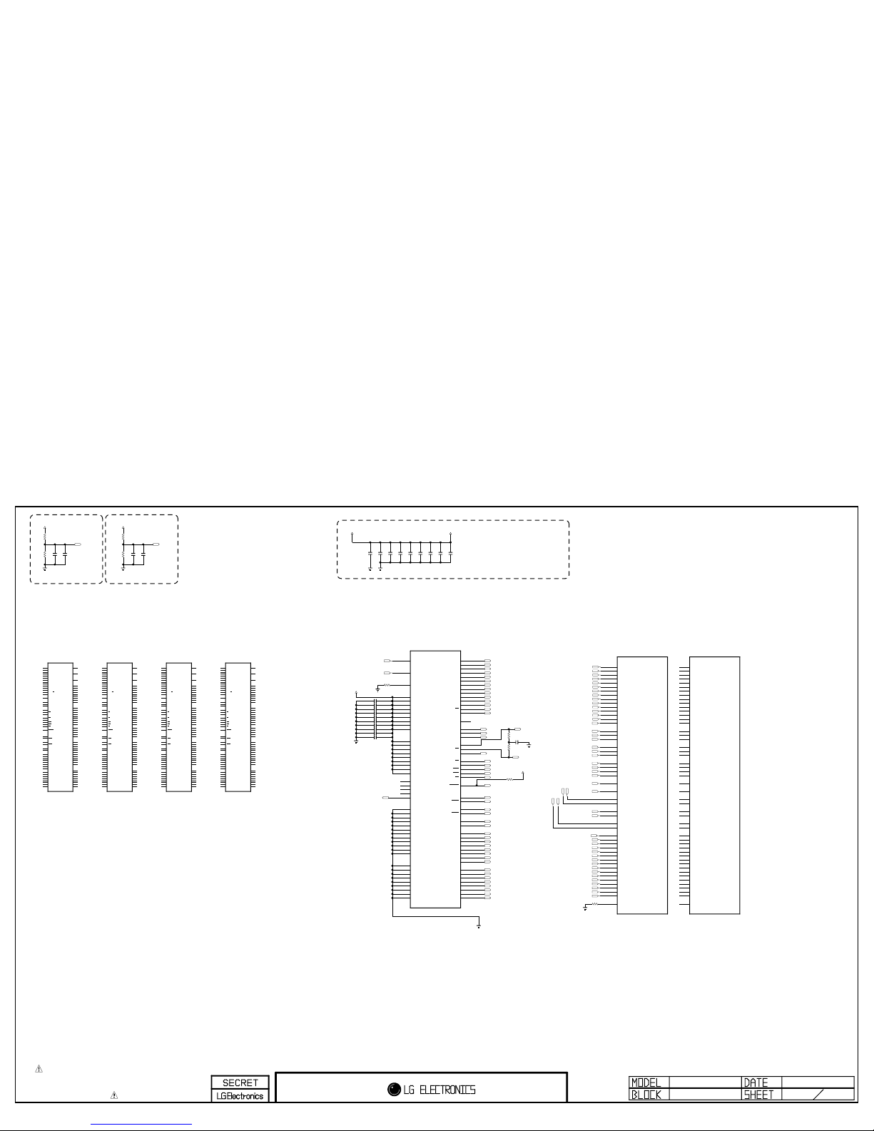
CI_TS_DATA[0]
PCM_D[6]
PCM_5V_CTL
/PCM_CE
SC1_FB
CI_TS_CLK
PCM_A[10]
PCM_A[9]
HP_LOUT
CI_TS_DATA[2]
CI_TS_SYNC
PCM_A[13]
SC1_IDPCM_D[1]
HP_DET
SCART1_MUTE
PCM_D[5]
/PCM_WE
/PCM_IRQA
PCM_D[3]
PCM_D[0]
/PCM_CD
CI_TS_DATA[5]
PCM_D[2]
PCM_A[14]
CI_TS_DATA[4]
SCART1_Lout
/PCM_REG
HP_ROUT
/PCM_IOWR CI_TS_DATA[1]
PCM_RST
PCM_A[12]
CI_TS_VAL
CI_TS_DATA[3]
/PCM_WAIT
SCART1_Rout
CI_TS_DATA[6]
PCM_D[4]
PCM_A[8]
DTV/MNT_VOUT
PCM_D[7]
/PCM_OE
SIDE_HP_MUTE
CI_TS_DATA[7]
/PCM_IORD PCM_A[11]
SC1_B+/COMP1_Pb+
SC1_G+/COMP1_Y+
SC1_R+/COMP1_Pr+
SC1/COMP1_L_IN
SC1/COMP1_DET
SC1/COMP1_R_IN
FE_TS_DATA[1]
FE_TS_DATA[2]
FE_TS_DATA[3]
FE_TS_DATA[4]
FE_TS_DATA[5]
FE_TS_DATA[6]
FE_TS_DATA[7]
/CI_DET
2013.05.09
TP_NON_EN
3
NC5_L14
TP for Headphone
TP for S2
TP for CI slot
TP for NON-EU models(except EU and China)
TP for SCART
TP for FE_TS_DATA
Copyright © 2013 LG Electronics. Inc. All rights reserved.
Only for training and service purposes
LGE Internal Use Only
THERMAL
THERMAL
THE SYMBOL MARK OF THIS SCHEMETIC DIAGRAM INCORPORATES
SPECIAL FEATURES IMPORTANT FOR PROTECTION FROM X-RADIATION.
FIRE AND ELECTRICAL SHOCK HAZARDS, WHEN SERVICING IF IS
ESSENTIAL THAT ONLY MANUFACTURES SPECIFIED PARTS BE USED FOR
THE CRITICAL COMPONENTS IN THE SYMBOL MARK OF THE SCHEMETIC.
Power_PD2
2013.10.28
4
L14_M1A
Q403
MMBT3904(NXP)
E
B
C
+12V
R426
10K
+3.5V_ST
Q406
AO3435
FET_2.5V_AOS
G
D
S
PANEL_VCC
PWM_DIM
Q400
MMBT3904(NXP)
E
B
C
R420
1K
R424
3.9K
PWM_DIM_PULL_DOWN
R401
10K
R442
10K
+24V
Q404
MMBT3904(NXP)
E
B
C
R441
10K
+3.5V_ST
R445
33K
R448
2.2K
C413
0.1uF
16V
OPT
C416
0.33uF
16V
R444
10K
+12V
INV_CTL
R430
2.7K
1%
+3.5V_ST
R400
10K
OPT
+3.5V_ST
R425
10K
R435
100K
Q402
MMBT3904(NXP)
E
B
C
R429
10K
C415
0.1uF
16V
C417
0.1uF
16V
L410
BLM18PG121SN1D
C424
0.1uF
16V
OPT
+3.3V_Normal
Q406-*1
DMP2130L
FET_2.5V_DIODE
G
D
S
R432
0
5%
OPT
R431
1.2K
1%
L403
MLB-201209-0120P-N2
POWER_ON/OFF_1
C401
0.1uF
50V
+1.10V_VDDC
POWER_DET
RL_ON
+3.3V_Normal
+12V
+24V
+3.5V_ST
L402
MLB-201209-0120P-N2
C429
0.1uF
16V
R423
100
PWM2_2CH_POWER
PANEL_CTL
R443
10K
R406
10K
R419
100
+3.5V_ST
POWER_DET_RESET
+3.3V_Normal
C402
0.1uF
16V
C425
0.1uF
25V
OPT
C422
0.1uF
R436
100K
OPT
R451
5.6K
R404
4.7K
R402
10K
R452
5.6K
R412
33K
OPT
Q401
MMBT3906(NXP)
1
2
3
PWM1
L407
3.6uH
R454
100 5%
PD_+12V
C430
22uF
10V
C414
10uF
10V
C428
2.2uF
10V
C420
22uF
10V
C421
22uF
10V
C427
10uF
16V
ZD400
5V
ZD402
5V
L401
CB2012PK501T
L400
CB2012PK501T
L408
UBW2012-121F
120OHM
+3.3V_Normal
C406
10uF
16V
R418
10
R410
100K
L405
4.7uH
R405
4.7K
OPT
R409
10K
C408
10uF
10V
+3.3V_Normal
R416
100K
OPT
AVDD5V_MHL
+5V_Normal
USB1_OCD
C412
22uF
16V
+5V_USB
10uF
C405
R407
10K
R403
4.7K
OPT
5V_HDMI_4
USB1_CTL
+12V
/MHL_OCP_DET
C409
0.047uF
25V
L409
BLM18PG121SN1D
+3.3V_Normal
L411
CB2012PK501T
10uF
C426
10V
+1.5V_DDR
10uF
C431
10V
R455
0
C410
10uF
10V
ZD403
2.5V
ZD401
2.5V
R456
0
OPT
C432
4.7uF
50V
3216
+24V_CAP
C400
1uF
10V
1005
OPT
+24V
R457
8.2K
1%
OPT
R458
0
5%
OPT
R438
4.7K
OPT
C407
10uF
10V
2012
IC401
APX803D29
1
GND
3
VCC2RESET
IC402
APX803D29
OPT
1
GND
3
VCC2RESET
C434
390pF
50V
C419
0.039uF
50V
C423
270pF
50V
C435
0.1uF
16V
C418
0.01uF
ZD404
5V
+3.5V_POWER_DET
+3.5V_POWER_DET
+3.5V_POWER_DET
+3.3V_Normal
/VBUS_EN
MHL_OCP_EN
R463
2.7K
MHL_SW_TR
R464
10K
MHL_SW_TR
Q408
MHL_SW_TR
E
B
C
R462
10K
MHL_SW_TR
Q407
MHL_SW_TR
E
B
C
Q409
MHL_SW_TR
E
B
C
R465
10K
MHL_SW_TR
R466
20K
R461
10K
MHL_SW_TR
R439
20K
1%
R440
47K
1%
R433
2.7K
1%
R447
22K
C403
100pF
50V
OPT
R415
15K
5%
R459
0
OPT
R408
4.7K
R449
1K
1/16W
1%
R450
200
1/16W
1%
C411
82pF
50V
C404
4700pF
50V
D401
30V
MBR230LSFT1G
L406
CB2012PK501T
+3.5V_ST
C436
10uF
10V
OPT
C437
0.1uF
16V
Q405
DMP2130L
G
D
S
R427
27K
1%
OPT
R428
5.1K
1%
OPT
IC404
AZ1117EH-ADJTRG1
ADJ/GND
OUTIN
R437
100 5%
OPT
R454-*1
300
5%
PD_+3.5V
IC403
TPS5432DDAR
3
PH
2
VIN
4
GND
1
BOOT
5
VSENSE
6
COMP
7
EN
8
SS
9
[EP]GND
TPS65282REGR
IC400
1
EN
3
SS
7
FAULT2
9
SW_OUT2
10
RLIM11AGND
12
SW_OUT1
13
SW_IN_1
14
SW_IN_2
15
FB
16
LX_1
17
LX_2
18
BST
19
PGND_120PGND_221VIN_122VIN_223PGOOD24V7V
5
EN_SW2
8
FAULT1
6
EN_SW1
4
ROSC
2
COMP
25
[EP]GND
C433
4.7uF
16V
+12V_CAP
3216
MHL_5V_EN
MHL_5V_EN
R421
18K
1%
R422
3.3K
1%
P401
SMAW200-H18S5
14
12V
9
24V
4
PDIM#1
18
GND
13
12V
8
PDMI#2
3
3.5V
17
GND
12
GND
7
GND
2
DRV ON
16
NC
11
GND
6
3.5V
1
PWR ON
15
12V
10
24V
5
3.5V
19
.
R446
12K
R453
0
R467
1K
OPT
PANEL_VCC
+1.10V_VDDC
R1
+3.3V_Normal
+1.5V_DDR
Vout=0.808*(1+R1/R2)
Power_DET
R2
FROM LIPS or POWER B/D
L14 POWER BLOCK (POWER DETECT 2)
R1
R2
+5V_Normal & +5V_USB with OCP
R2
R1
1.3A
4A
Vout=1.25*(1+R2/R1)+Iadj*R2
Vout=0.8*(1+R1/R2)
3A
(Active High)
(Active Low)
Ready - Dual Power Det
R432, R454-*1, R438
Now is
R457, R454
Detect Valtage
O R430, R431, R454
Use Circuit Designator
Power Detect +3.5V
Power Detect +12V
Power Detect +24V
Power Detect activity
* Notice
- Applying all inch models for LCD L14
- Dual Power Det is used
for detecting two kinds of voltage
Copyright © 2013 LG Electronics. Inc. All rights reserved.
Only for training and service purposes
LGE Internal Use Only
USB D OWN STREA M
THE SYMBOL MARK OF THIS SCHEMETIC DIAGRAM INCORPORATES
SPECIAL FEATURES IMPORTANT FOR PROTECTION FROM X-RADIATION.
FIRE AND ELECTRICAL SHOCK HAZARDS, WHEN SERVICING IF IS
ESSENTIAL THAT ONLY MANUFACTURES SPECIFIED PARTS BE USED FOR
THE CRITICAL COMPONENTS IN THE SYMBOL MARK OF THE SCHEMETIC.
13/04/30
USB_S1
7
L14_M1A
JK700
3AU04 S-305-ZC- (LG)
1234
5
D700
RCLAMP0502BA
OPT
SIDE_USB1_DM
SIDE_USB1_DP
C700
22uF
10V
ZD700
5V
OPT
SD05
C701
5pF
50V
OPT
C702
5pF
50V
OPT
C703
22uF
10V
USB_HDD_CAP
+5V_USB
USB (SIDE)
Copyright © 2013 LG Electronics. Inc. All rights reserved.
Only for training and service purposes
LGE Internal Use Only
THE SYMBOL MARK OF THIS SCHEMETIC DIAGRAM INCORPORATES
SPECIAL FEATURES IMPORTANT FOR PROTECTION FROM X-RADIATION.
FIRE AND ELECTRICAL SHOCK HAZARDS, WHEN SERVICING IF IS
ESSENTIAL THAT ONLY MANUFACTURES SPECIFIED PARTS BE USED FOR
THE CRITICAL COMPONENTS IN THE SYMBOL MARK OF THE SCHEMETIC.
2013/08/15
HDMI_R1_S1 8
L14_M1A
VA804
ESD_HDMI1
R803
1K
D802
MMBD6100
A2CA1
HDMI_ARC
VA805
ESD_HDMI2
D1+_HDMI2
CEC_REMOTE_S7
+3.5V_ST
VA800
ESD_HDMI1_VARISTOR
VA808
ESD_HDMI2
R809
10K
D2-_HDMI2
VA802
ESD_HDMI1
R807
2.7K
D801
MMBD6100
A2CA1
CK-_HDMI4
CK-_HDMI2
R804
100
VA801
ESD_HDMI1_VARISTOR
R816 100
HDMI-2
R810 100
DDC_SCL_2
R812
1.8K
HDMI-2
DDC_SCL_2
JK800
EAG59023302
14
13
5
D1_GND
20
SHIELD
12
11
2
D2_GND
19
18
10
CK+
4
D1+
1
D2+
17
9
D0-
8
D0_GND
3
D2-
16
7
D0+
6
D1-
15
D0+_HDMI2
R811 100
VA803
ESD_HDMI1
DDC_SDA_2
5V_HDMI_2
R800
2.7K
HPD4
5V_HDMI_4
CK+_HDMI4
D800
MMBD6100
A2CA1
VA809
ESD_HDMI2
VA800-*1
1uF
10V
ESD_HDMI1_CAP
+5V_Normal
R805
3.3K
DDC_SCL_4
VA801-*1
1uF
10V
ESD_HDMI1_CAP
R814
33
HDMI-2
D1-_HDMI4
DDC_SDA_4
5V_DET_HDMI_4
5V_HDMI_4
D1-_HDMI2
HDMI_CEC
CK+_HDMI2
R806
2.7K
R817
300K
HDMI-2
5V_DET_HDMI_2
DDC_SDA_4
+5V_Normal
DDC_SCL_4
HPD2
HDMI_CEC
Q800
MMBT3904(NXP)
E
B
C
R801
2.7K
D0-_HDMI2
VA811
ESD_HDMI2
D0-_HDMI4
MHL_CD_SENSE
5V_HDMI_2
R813
3.3K
HDMI-2
VA810
ESD_HDMI2
D2+_HDMI4
VA807
OPT
5.6V
DDC_SDA_2
D1+_HDMI4
R815 100
HDMI-2
C800
0.047uF
25V
HDMI-2
D2-_HDMI4
R802
1.8K
D2+_HDMI2
R808
10K
HDMI_CEC
D0+_HDMI4
VA806
ESD_HDMI2
JK801
EAG62611204
HDMI-2
14
NC
13
CE_REMOTE
5
D1_GND
20
GND
12
CK-
11
CK_GND
2
D2_GND
19
HP_DET
18
5V
10
CK+
4
D1+
1
D2+
17
GND
9
D0-
8
D0_GND
3
D2-
16
DDC_DATA
7
D0+
6
D1-
15
DDC_CLK
D803-*2
RCLAMP0524PA
ESD_HDMI1_SEMTECH
1
8
2
7
3
645
9
10
D804-*2
RCLAMP0524PA
ESD_HDMI1_SEMTECH
1
8
2
7
3
645
9
10
D806-*2
RCLAMP0524PA
ESD_HDMI2_SEMTECH
1
8
2
7
3
645
9
10
D805-*2
RCLAMP0524PA
ESD_HDMI2_SEMTECH
1
8
2
7
3
645
9
10
JK801-*1
DAADR019A
HDMI-2_EMI_FOOSUNG
14
RESERVED
13
CEC
5
TMDS_DATA1_SHIELD
20
BODY_SHIELD
12
TMDS_CLK-
11
TMDS_CLK_SHIELD
2
TMDS_DATA2_SHIELD
19
HOT_PLUG_DETECT
18
VDD[+5V]
10
TMDS_CLK+
4
TMDS_DATA1+
1
TMDS_DATA2+
17
DDC/CEC_GND
9
TMDS_DATA0-
8
TMDS_DATA0_SHIELD
3
TMDS_DATA2-
16
SDA
7
TMDS_DATA0+
6
TMDS_DATA1-
15
SCL
D803
IP4294CZ10-TBR
ESD_HDMI1_IP4294
1
8
2
7
3
6
4
5
9
10
D803-*1
IP4283CZ10-TBA
ESD_HDMI1_IP4283
3
GND_1
2
TMDS_CH1+
4
TMDS_CH2-
1
TMDS_CH1-
5
TMDS_CH2+6NC_1
7
NC_2
8
GND_2
9
NC_3
10
NC_4
D804-*1
IP4283CZ10-TBA
ESD_HDMI1_IP4283
3
GND_1
2
TMDS_CH1+
4
TMDS_CH2-
1
TMDS_CH1-
5
TMDS_CH2+6NC_1
7
NC_2
8
GND_2
9
NC_3
10
NC_4
D805-*1
IP4283CZ10-TBA
ESD_HDMI2_IP4283
3
GND_1
2
TMDS_CH1+
4
TMDS_CH2-
1
TMDS_CH1-
5
TMDS_CH2+6NC_1
7
NC_2
8
GND_2
9
NC_3
10
NC_4
D806-*1
IP4283CZ10-TBA
ESD_HDMI2_IP4283
3
GND_1
2
TMDS_CH1+
4
TMDS_CH2-
1
TMDS_CH1-
5
TMDS_CH2+6NC_1
7
NC_2
8
GND_2
9
NC_3
10
NC_4
D804
IP4294CZ10-TBR
ESD_HDMI1_IP4294
1
8
2
7
3
6
4
5
9
10
D805
IP4294CZ10-TBR
ESD_HDMI2_IP4294
1
8
2
7
3
6
4
5
9
10
D806
IP4294CZ10-TBR
ESD_HDMI2_IP4294
1
8
2
7
3
6
4
5
9
10
HDMI (REAR 1 / SIDE 1 MHL)
HDMI_2 MHL
HDMI_1
CEC
MHL Spec
Copyright © 2013 LG Electronics. Inc. All rights reserved.
Only for training and service purposes
LGE Internal Use Only
Fiber Optic
THE SYMBOL MARK OF THIS SCHEMETIC DIAGRAM INCORPORATES
SPECIAL FEATURES IMPORTANT FOR PROTECTION FROM X-RADIATION.
FIRE AND ELECTRICAL SHOCK HAZARDS, WHEN SERVICING IF IS
ESSENTIAL THAT ONLY MANUFACTURES SPECIFIED PARTS BE USED FOR
THE CRITICAL COMPONENTS IN THE SYMBOL MARK OF THE SCHEMETIC.
SPDIF
2013/10/29
10
NC5_L14
+3.3V_Normal
SPDIF_OUT
JK1001
JST1223-001
SPDIF_OPTIC
1
GND
2
VCC
3
VINPUT
4
FIX_POLE
C1001
1uF
10V
OPT
C1002
47pF
50V
SPDIF_CAP_47pF
C1002-*1
18pF
50V
SPDIF_CAP_18pF
SPDIF OPTIC JACK
5.15 Mstar Circuit Application
SPDIF
ESD Ready
Copyright © 2013 LG Electronics. Inc. All rights reserved.
Only for training and service purposes
LGE Internal Use Only
THE SYMBOL MARK OF THIS SCHEMETIC DIAGRAM INCORPORATES
SPECIAL FEATURES IMPORTANT FOR PROTECTION FROM X-RADIATION.
FIRE AND ELECTRICAL SHOCK HAZARDS, WHEN SERVICING IF IS
ESSENTIAL THAT ONLY MANUFACTURES SPECIFIED PARTS BE USED FOR
THE CRITICAL COMPONENTS IN THE SYMBOL MARK OF THE SCHEMETIC.
LVDS_NON_EU
2013/05/22
11
L14_S7LR(M1A)
RXB0-
RXA0+
C1101
0.1uF
16V
MO_HD
C1100
0.1uF
16V
MO_FHD
RXBCK-
RXA1-
RXB4-
+3.3V_Normal
RXB1+
RXBCK+
PANEL_VCC
RXB3+
RXA3-
RXB4+
RXA4-
RXA4+
RXA2+
RXB2-
RXA1+
RXA2-
RXB1-
R1109
3.3K
OPT
RXA3+
RXA0-
PANEL_VCC
RXACK-
RXB2+
R1110
10K
OPT
RXB3-
RXB0+
P1100
FI-RE51S-HF-J-R1500
MO_FHD
1
.
2
.
3
.
4
.
5
.
6
.
7
.
8
.
9
.
10
.
11
.
12
RXA0-
13
RXA0+
14
RXA1-
15
RXA1+
16
RXA2-
17
RXA2+
18
.
19
RXACK-
20
RXACK+
21
.
22
RXA3-
23
RXA3+
24
RXA4-
25
RXA4+
26
.
27
.
28
RXB0-
29
RXB0+
30
RXB1-
31
RXB1+
32
RXB2-
33
RXB2+
34
.
35
RXBCK-
36
RXBCK-
37
.
38
RXB3-
39
RXB3+
40
RXB4-
41
RXB4+
42
.
43
.
44
.
45
.
46
.
47
.
48
.
49
.
50
.
51
.
52
.
RXACK+
R1100 0
MO_FHD
R1101 0
MO_FHD
R1102 0
MO_FHD
R1104
10K
OPT
R1103
3.3K
OPT
+3.3V_Normal
L1101
UBW2012-121F
120OHM
MO_HD
L1100
UBW2012-121F
120OHM
MO_FHD
RXA3+
RXA3-
RXACK+
RXACK-
RXA2-
RXA2+
RXA1-
RXA1+
RXA0-
RXA0+
VCOM_SCL
VCOM_SDA
VCOM_SCL
VCOM_SDA
R1115
2K
VCOM_I2C_PULL_UP
VCOM_SCL
VCOM_SDA
R1114
2K
VCOM_I2C_PULL_UP
R1105
0
VCOM_I2C
URSA/VCOM_SDA
URSA/VCOM_SCL
R1106
0
VCOM_I2C
+3.3V_Normal
URSA/VCOM_SDA
URSA/VCOM_SCL
P1101
10031HR-30
MO_HD
1
2
3
4
5
6
7
8
9
10
11
12
13
14
15
16
17
18
19
20
21
22
23
24
25
26
27
28
29
30
31
RXB1-
RXB0-
RXA4+
RXA1-
Pol-change
RXB4+
RXACK+
RXBCK-
RXA0+
RXA2+
LVDS (NON EU)
RXA2+
RXBCK-
RXB4-
RXA3+
RXA1+
RXB2+
RXB3-
RXA3-
RXBCK-
RXACK-
RXA2+
RXA1-
RXB1-
RXB3-
RXA3+
RXA2-
RXA0+
RXA4+
Shift
RXBCK+
RXB2-
RXA4+
[51Pin LVDS Connector]
(For FHD 60Hz)
RXACK+
RXA3-
RXACK-
RXB3+
RXA3+
RXA1-
RXB0-
RXA0-
RXACK+
RXB3+
RXA4-
RXB3+
RXA4+
RXA2-
RXA2+
RXA1+
RXB2-
Pol-change
RXB4+
RXB1-
RXA4-
RXACK+
RXB3-
RXB0+
RXB3+
RXBCK+
RXB4-
RXA0+
RXA2+
RXB0+
RXB1+
RXA3-
RXA2-
RXBCK+
RXB4-
RXA0+
RXA4+
RXA2+
RXB3-
RXA0-
RXB0-
RXA4-
RXACK-
RXB0-
RXA4+
RXB2+
RXA1-
RXB2+
RXACK-
RXA3-
RXA1+
RXA3-
RXA1+
RXB3+
RXB3-
RXA3-
RXB1-
RXB4+
FOR FHD REVERSE(10bit)
RXB0+
RXB3-
RXA3+
RXA0+
RXA2- RXACK-
RXB1-
RXA3+
RXB2- RXBCK-
RXBCK+
RXA1+
RXA0-
RXA3+
RXA0-
RXB2+
RXB0-
RXA0-
RXB2-
RXACK-
MIRROR
RXB4-
RXA0-
RXB2+
RXA4+
RXB4-
RXA1+
RXB3+
RXB0+
RXB1+
RXA1-
RXA0-
RXA4-
RXB2-
Change in S7LR
RXA4-
RXB2+
MIRROR
RXB1-
RXA3+
RXA1-
RXACK+
RXB3+
RXB0+
RXB4-
RXACK+
RXB1+
RXACK-
RXA4-
RXA1-
RXA2-
RXA0+
RXB0-
RXB1+
RXB4+
RXB2+
RXBCK-
RXB0-
FOR FHD REVERSE(8bit)
RXBCK-
RXBCK+
RXB4+
RXB0+
RXB2-
RXA1+
RXBCK-
RXA2-
RXB1+
RXB1+
RXB1-
RXA4-
RXB4+
[30Pin LVDS Connector]
(For HD 60Hz_Normal)
Change in S7LR
RXB1+
RXB3-
RXA2+
RXA3-
RXA2-
RXB2-
LVDS_SEL
RXBCK+
RXB4-
RXB0+
RXA0+
RXB4+
RXBCK+
RXACK+
EU pin assign is different from NON EU.
Because of position of HD wafer.
LVDS_SEL
V-COM I2C
Copyright © 2013 LG Electronics. Inc. All rights reserved.
Only for training and service purposes
LGE Internal Use Only
THE SYMBOL MARK OF THIS SCHEMETIC DIAGRAM INCORPORATES
SPECIAL FEATURES IMPORTANT FOR PROTECTION FROM X-RADIATION.
FIRE AND ELECTRICAL SHOCK HAZARDS, WHEN SERVICING IF IS
ESSENTIAL THAT ONLY MANUFACTURES SPECIFIED PARTS BE USED FOR
THE CRITICAL COMPONENTS IN THE SYMBOL MARK OF THE SCHEMETIC.
1_DDR
2013/05/20
12
NC5_S7LR(M1A)
A-MWEB
A-MA7
A-MDQL5
A-MBA2
A-MCASB
A-MA8
A-MA12
R1208
56 1%
DDR_EXT
A-MODT
A-MA2
A-MDQU7
A-MDQL0
A-MDQL2
C12010.1uF
DDR_EXT
A-MA14
C1202 1000pF
DDR_EXT
A-MDQSLB
A-MA4
R12011K1%
DDR_EXT
A-MVREFDQ
A-MRESETB
A-MCKB
A-MDQL3
A-MDMU
A-MVREFCA
R1202 1K1%
DDR_EXT
A-MDQL4
A-MBA1
R1205 1K 1%
DDR_EXT
A-MDQU2
R1203
240
1%
DDR_EXT
A-MDQSU
R1206
10K
DDR_EXT
A-MBA0
A-MA5
A-MDQU1
A-MDQSL
A-MA9
R1207
56 1%
DDR_EXT
C1214
1000pF
DDR_EXT
A-MCKE
A-MVREFDQ
A-MDML
A-MA10
A-MDQU0
A-MA13
A-MDQU3
A-MA11
A-MDQU6
A-MDQSUB
C12130.1uF
DDR_EXT
A-MRASB
A-MVREFCA
A-MDQU4
A-MDQU5
A-MDQL7
A-MA0
A-MDQL6
A-MA3
A-MDQL1
A-MA1
A-MA6
A-MCK
R1204 1K 1%
DDR_EXT
+1.5V_DDR
C1217
0.1uF
OPT
C1210 0.1uF
DDR_EXT
C1206 0.1uF
DDR_EXT
C1211 0.1uF
DDR_EXT
C1207 0.1uF
DDR_EXT
C1208 0.1uF
DDR_EXT
C1204 0.1uF
DDR_EXT
C1212 0.1uF
DDR_EXT
C1209 0.1uF
DDR_EXT
C1205 0.1uF
DDR_EXT
C1215
0.01uF
50V
DDR_EXT
C1218
0.1uF
OPT
C1224
0.1uF
OPT
H5TQ2G63DFR-PBC
IC1201-*2
DDR_1600_2G_HYNIX_OLD
EAN61829203
A0
N3
A1
P7
A2
P3
A3
N2
A4
P8
A5
P2
A6
R8
A7
R2
A8
T8
A9
R3
A10/AP
L7
A11
R7
A12/BC
N7
A13
T3
NC_5
M7
BA0
M2
BA1
N8
BA2
M3
CK
J7
CK
K7
CKE
K9
CS
L2
ODT
K1
RAS
J3
CAS
K3
WE
L3
RESET
T2
DQSL
F3
DQSL
G3
DQSU
C7
DQSU
B7
DML
E7
DMU
D3
DQL0
E3
DQL1
F7
DQL2
F2
DQL3
F8
DQL4
H3
DQL5
H8
DQL6
G2
DQL7
H7
DQU0
D7
DQU1
C3
DQU2
C8
DQU3
C2
DQU4
A7
DQU5
A2
DQU6
B8
DQU7
A3
VREFCA
M8
VREFDQ
H1
ZQ
L8
VDD_1
B2
VDD_2
D9
VDD_3
G7
VDD_4
K2
VDD_5
K8
VDD_6
N1
VDD_7
N9
VDD_8
R1
VDD_9
R9
VDDQ_1
A1
VDDQ_2
A8
VDDQ_3
C1
VDDQ_4
C9
VDDQ_5
D2
VDDQ_6
E9
VDDQ_7
F1
VDDQ_8
H2
VDDQ_9
H9
NC_1
J1
NC_2
J9
NC_3
L1
NC_4
L9
NC_6
T7
VSS_1
A9
VSS_2
B3
VSS_3
E1
VSS_4
G8
VSS_5
J2
VSS_6
J8
VSS_7
M1
VSS_8
M9
VSS_9
P1
VSS_10
P9
VSS_11
T1
VSS_12
T9
VSSQ_1
B1
VSSQ_2
B9
VSSQ_3
D1
VSSQ_4
D8
VSSQ_5
E2
VSSQ_6
E8
VSSQ_7
F9
VSSQ_8
G1
VSSQ_9
G9
C1216
10uF10V
OPT
C1203 10uF
10V
DDR_EXT
C1219
1uF
OPT
C1220
1uF
OPT
C1221
1uF
OPT
C1222
1uF
OPT
C1223
1uF
OPT
+1.5V_DDR
+1.5V_DDR
+1.5V_DDR
+1.5V_DDR+1.5V_DDR
A-MA13
A-MA14
A-MA7
A-MA10
A-MA1
A-MA8
A-MA3
A-MA0
A-MA4
A-MA6
A-MA11
A-MA9
A-MA5
A-MA2
A-MA12
A-MBA0
A-MBA1
A-MBA2
A-MCKE
A-MCK
A-MCKB
A-MCASB
A-MWEB
A-MRASB
A-MODT
A-MRESETB
A-MDMU
A-MDML
A-MDQSU
A-MDQSUB
A-MDQSL
A-MDQSLB
A-MDQL4
A-MDQL0
A-MDQL3
A-MDQL7
A-MDQL5
A-MDQL2
A-MDQL6
A-MDQL1
A-MDQU1
A-MDQU3
A-MDQU0
A-MDQU4
A-MDQU5
A-MDQU2
A-MDQU6
A-MDQU7
R1209
240
1%
A/B_DDR3_CS
A/B_DDR3_CS
H5TQ1G63EFR-PBC
IC1201
DDR_1600_1G_HYNIX
EAN61829003
A0
N3
A1
P7
A2
P3
A3
N2
A4
P8
A5
P2
A6
R8
A7
R2
A8
T8
A9
R3
A10/AP
L7
A11
R7
A12/BC
N7
NC_7
T3
NC_5
M7
BA0
M2
BA1
N8
BA2
M3
CK
J7
CK
K7
CKE
K9
CS
L2
ODT
K1
RAS
J3
CAS
K3
WE
L3
RESET
T2
DQSL
F3
DQSL
G3
DQSU
C7
DQSU
B7
DML
E7
DMU
D3
DQL0
E3
DQL1
F7
DQL2
F2
DQL3
F8
DQL4
H3
DQL5
H8
DQL6
G2
DQL7
H7
DQU0
D7
DQU1
C3
DQU2
C8
DQU3
C2
DQU4
A7
DQU5
A2
DQU6
B8
DQU7
A3
VREFCA
M8
VREFDQ
H1
ZQ
L8
VDD_1
B2
VDD_2
D9
VDD_3
G7
VDD_4
K2
VDD_5
K8
VDD_6
N1
VDD_7
N9
VDD_8
R1
VDD_9
R9
VDDQ_1
A1
VDDQ_2
A8
VDDQ_3
C1
VDDQ_4
C9
VDDQ_5
D2
VDDQ_6
E9
VDDQ_7
F1
VDDQ_8
H2
VDDQ_9
H9
NC_1
J1
NC_2
J9
NC_3
L1
NC_4
L9
NC_6
T7
VSS_1
A9
VSS_2
B3
VSS_3
E1
VSS_4
G8
VSS_5
J2
VSS_6
J8
VSS_7
M1
VSS_8
M9
VSS_9
P1
VSS_10
P9
VSS_11
T1
VSS_12
T9
VSSQ_1
B1
VSSQ_2
B9
VSSQ_3
D1
VSSQ_4
D8
VSSQ_5
E2
VSSQ_6
E8
VSSQ_7
F9
VSSQ_8
G1
VSSQ_9
G9
IC101
LGE2132(M1A_256M)
M1A_256M
B_DDR3_A[0]
E11
B_DDR3_A[1]
F12
B_DDR3_A[2]
D10
B_DDR3_A[3]
B10
B_DDR3_A[4]
E15
B_DDR3_A[5]
B11
B_DDR3_A[6]
F14
B_DDR3_A[7]
C11
B_DDR3_A[8]
D14
B_DDR3_A[9]
A12
B_DDR3_A[10]
F16
B_DDR3_A[11]
D13
B_DDR3_A[12]
D15
B_DDR3_A[13]
C12
B_DDR3_A[14]
E13
B_DDR3_BA[0]
A9
B_DDR3_BA[1]
D16
B_DDR3_BA[2]
A10
B_DDR3_MCLK
C13
B_DDR3_MCLKZ
B13
B_DDR3_MCLKE
E17
B_DDR3_ODT
B8
B_DDR3_RASZ
C8
B_DDR3_CASZ
B9
B_DDR3_WEZ
D11
B_RESET
F10
B_DDR3_CS0
D12
B_DDR3_DQSL
A19
B_DDR3_DQSU
B18
B_DDR3_DQML
C16
B_DDR3_DQMU
D21
B_DDR3_DQSBL
C18
B_DDR3_DQSBU
C17
B_DDR3_DQL[0]
A20
B_DDR3_DQL[1]
A16
B_DDR3_DQL[2]
C19
B_DDR3_DQL[3]
C15
B_DDR3_DQL[4]
C20
B_DDR3_DQL[5]
C14
B_DDR3_DQL[6]
B21
B_DDR3_DQL[7]
B15
B_DDR3_DQU[0]
F18
B_DDR3_DQU[1]
D19
B_DDR3_DQU[2]
D17
B_DDR3_DQU[3]
E21
B_DDR3_DQU[4]
E19
B_DDR3_DQU[5]
D20
B_DDR3_DQU[6]
D18
B_DDR3_DQU[7]
F20
ZQ
E9
IC101-*1
LGE2131(M1A_128M)
M1A_128M
B_DDR3_A[0]
E11
B_DDR3_A[1]
F12
B_DDR3_A[2]
D10
B_DDR3_A[3]
B10
B_DDR3_A[4]
E15
B_DDR3_A[5]
B11
B_DDR3_A[6]
F14
B_DDR3_A[7]
C11
B_DDR3_A[8]
D14
B_DDR3_A[9]
A12
B_DDR3_A[10]
F16
B_DDR3_A[11]
D13
B_DDR3_A[12]
D15
B_DDR3_A[13]
C12
B_DDR3_A[14]
E13
B_DDR3_BA[0]
A9
B_DDR3_BA[1]
D16
B_DDR3_BA[2]
A10
B_DDR3_MCLK
C13
B_DDR3_MCLKZ
B13
B_DDR3_MCLKE
E17
B_DDR3_ODT
B8
B_DDR3_RASZ
C8
B_DDR3_CASZ
B9
B_DDR3_WEZ
D11
B_RESET
F10
B_DDR3_CS0
D12
B_DDR3_DQSL
A19
B_DDR3_DQSU
B18
B_DDR3_DQML
C16
B_DDR3_DQMU
D21
B_DDR3_DQSBL
C18
B_DDR3_DQSBU
C17
B_DDR3_DQL[0]
A20
B_DDR3_DQL[1]
A16
B_DDR3_DQL[2]
C19
B_DDR3_DQL[3]
C15
B_DDR3_DQL[4]
C20
B_DDR3_DQL[5]
C14
B_DDR3_DQL[6]
B21
B_DDR3_DQL[7]
B15
B_DDR3_DQU[0]
F18
B_DDR3_DQU[1]
D19
B_DDR3_DQU[2]
D17
B_DDR3_DQU[3]
E21
B_DDR3_DQU[4]
E19
B_DDR3_DQU[5]
D20
B_DDR3_DQU[6]
D18
B_DDR3_DQU[7]
F20
ZQ
E9
H5TQ2G63FFR-PBC
IC1201-*3
DDR_1600_2G_HYNIX_NEW
EAN61829204
A0
N3
A1
P7
A2
P3
A3
N2
A4
P8
A5
P2
A6
R8
A7
R2
A8
T8
A9
R3
A10/AP
L7
A11
R7
A12/BC
N7
A13
T3
NC_5
M7
BA0
M2
BA1
N8
BA2
M3
CK
J7
CK
K7
CKE
K9
CS
L2
ODT
K1
RAS
J3
CAS
K3
WE
L3
RESET
T2
DQSL
F3
DQSL
G3
DQSU
C7
DQSU
B7
DML
E7
DMU
D3
DQL0
E3
DQL1
F7
DQL2
F2
DQL3
F8
DQL4
H3
DQL5
H8
DQL6
G2
DQL7
H7
DQU0
D7
DQU1
C3
DQU2
C8
DQU3
C2
DQU4
A7
DQU5
A2
DQU6
B8
DQU7
A3
VREFCA
M8
VREFDQ
H1
ZQ
L8
VDD_1
B2
VDD_2
D9
VDD_3
G7
VDD_4
K2
VDD_5
K8
VDD_6
N1
VDD_7
N9
VDD_8
R1
VDD_9
R9
VDDQ_1
A1
VDDQ_2
A8
VDDQ_3
C1
VDDQ_4
C9
VDDQ_5
D2
VDDQ_6
E9
VDDQ_7
F1
VDDQ_8
H2
VDDQ_9
H9
NC_1
J1
NC_2
J9
NC_3
L1
NC_4
L9
NC_6
T7
VSS_1
A9
VSS_2
B3
VSS_3
E1
VSS_4
G8
VSS_5
J2
VSS_6
J8
VSS_7
M1
VSS_8
M9
VSS_9
P1
VSS_10
P9
VSS_11
T1
VSS_12
T9
VSSQ_1
B1
VSSQ_2
B9
VSSQ_3
D1
VSSQ_4
D8
VSSQ_5
E2
VSSQ_6
E8
VSSQ_7
F9
VSSQ_8
G1
VSSQ_9
G9
K4B1G1646G-BCK0
IC1201-*1
DDR_1600_1G_SS
EAN61836301
A0
N3
A1
P7
A2
P3
A3
N2
A4
P8
A5
P2
A6
R8
A7
R2
A8
T8
A9
R3
A10/AP
L7
A11
R7
A12/BC
N7
A13
T3
NC_5
M7
BA0
M2
BA1
N8
BA2
M3
CK
J7
CK
K7
CKE
K9
CS
L2
ODT
K1
RAS
J3
CAS
K3
WE
L3
RESET
T2
DQSL
F3
DQSL
G3
DQSU
C7
DQSU
B7
DML
E7
DMU
D3
DQL0
E3
DQL1
F7
DQL2
F2
DQL3
F8
DQL4
H3
DQL5
H8
DQL6
G2
DQL7
H7
DQU0
D7
DQU1
C3
DQU2
C8
DQU3
C2
DQU4
A7
DQU5
A2
DQU6
B8
DQU7
A3
VREFCA
M8
VREFDQ
H1
ZQ
L8
VDD_1
B2
VDD_2
D9
VDD_3
G7
VDD_4
K2
VDD_5
K8
VDD_6
N1
VDD_7
N9
VDD_8
R1
VDD_9
R9
VDDQ_1
A1
VDDQ_2
A8
VDDQ_3
C1
VDDQ_4
C9
VDDQ_5
D2
VDDQ_6
E9
VDDQ_7
F1
VDDQ_8
H2
VDDQ_9
H9
NC_1
J1
NC_2
J9
NC_3
L1
NC_4
L9
NC_6
T7
VSS_1
A9
VSS_2
B3
VSS_3
E1
VSS_4
G8
VSS_5
J2
VSS_6
J8
VSS_7
M1
VSS_8
M9
VSS_9
P1
VSS_10
P9
VSS_11
T1
VSS_12
T9
VSSQ_1
B1
VSSQ_2
B9
VSSQ_3
D1
VSSQ_4
D8
VSSQ_5
E2
VSSQ_6
E8
VSSQ_7
F9
VSSQ_8
G1
VSSQ_9
G9
K4B2G1646Q-BCK0
IC1201-*4
DDR_1600_2G_SS
EAN61848803
A0
N3
A1
P7
A2
P3
A3
N2
A4
P8
A5
P2
A6
R8
A7
R2
A8
T8
A9
R3
A10/AP
L7
A11
R7
A12/BC
N7
A13
T3
NC_5
M7
BA0
M2
BA1
N8
BA2
M3
CK
J7
CK
K7
CKE
K9
CS
L2
ODT
K1
RAS
J3
CAS
K3
WE
L3
RESET
T2
DQSL
F3
DQSL
G3
DQSU
C7
DQSU
B7
DML
E7
DMU
D3
DQL0
E3
DQL1
F7
DQL2
F2
DQL3
F8
DQL4
H3
DQL5
H8
DQL6
G2
DQL7
H7
DQU0
D7
DQU1
C3
DQU2
C8
DQU3
C2
DQU4
A7
DQU5
A2
DQU6
B8
DQU7
A3
VREFCA
M8
VREFDQ
H1
ZQ
L8
VDD_1
B2
VDD_2
D9
VDD_3
G7
VDD_4
K2
VDD_5
K8
VDD_6
N1
VDD_7
N9
VDD_8
R1
VDD_9
R9
VDDQ_1
A1
VDDQ_2
A8
VDDQ_3
C1
VDDQ_4
C9
VDDQ_5
D2
VDDQ_6
E9
VDDQ_7
F1
VDDQ_8
H2
VDDQ_9
H9
NC_1
J1
NC_2
J9
NC_3
L1
NC_4
L9
NC_6
T7
VSS_1
A9
VSS_2
B3
VSS_3
E1
VSS_4
G8
VSS_5
J2
VSS_6
J8
VSS_7
M1
VSS_8
M9
VSS_9
P1
VSS_10
P9
VSS_11
T1
VSS_12
T9
VSSQ_1
B1
VSSQ_2
B9
VSSQ_3
D1
VSSQ_4
D8
VSSQ_5
E2
VSSQ_6
E8
VSSQ_7
F9
VSSQ_8
G1
VSSQ_9
G9
CLose to Saturn7M IC
CLose to DDR3
Option : Ripple Check !!!
Copyright © 2013 LG Electronics. Inc. All rights reserved.
Only for training and service purposes
LGE Internal Use Only
THE SYMBOL MARK OF THIS SCHEMETIC DIAGRAM INCORPORATES
SPECIAL FEATURES IMPORTANT FOR PROTECTION FROM X-RADIATION.
FIRE AND ELECTRICAL SHOCK HAZARDS, WHEN SERVICING IF IS
ESSENTIAL THAT ONLY MANUFACTURES SPECIFIED PARTS BE USED FOR
THE CRITICAL COMPONENTS IN THE SYMBOL MARK OF THE SCHEMETIC.
S_FLASH
2013/04/29
13
NC5_S7LR(M1A)
SPI_SCK
+3.5V_ST+3.5V_ST
C1300
0.1uF
R1301
4.7K
OPT
/SPI_CS
SPI_SDO
IC1300
MX25L8006EM2I-12G
SPI_FLASH_MACRONIX
3
WP#
2
SO/SIO1
4
GND
1
CS#
5
SI/SIO0
6
SCLK
7
HOLD#
8
VCC
R1302
33
R1300
10K
OPT
SPI_SDI
/FLASH_WP
IC1300-*1
W25Q80BVSSIG
SPI_FLASH_WINBOND
3
%WP[IO2]
2
DO[IO1]
4
GND
1
CS
5
DI[IO0]
6
CLK
7
HOLD[IO3]
8
VCC
+3.5V_ST
Serial Flash for SPI boot
Copyright © 2013 LG Electronics. Inc. All rights reserved.
Only for training and service purposes
LGE Internal Use Only
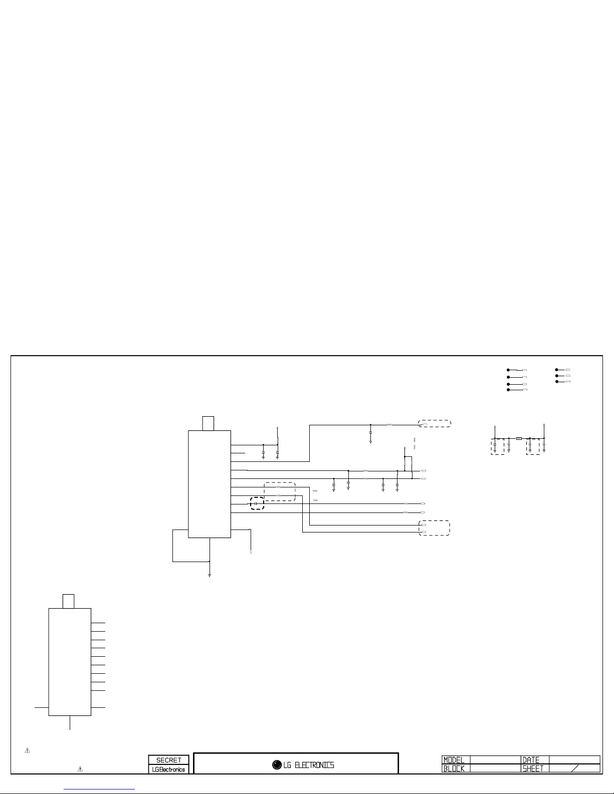
THE SYMBOL MARK OF THIS SCHEMETIC DIAGRAM INCORPORATES
SPECIAL FEATURES IMPORTANT FOR PROTECTION FROM X-RADIATION.
FIRE AND ELECTRICAL SHOCK HAZARDS, WHEN SERVICING IF IS
ESSENTIAL THAT ONLY MANUFACTURES SPECIFIED PARTS BE USED FOR
THE CRITICAL COMPONENTS IN THE SYMBOL MARK OF THE SCHEMETIC.
+3.3V_TU
C1613
20pF
50V
OPT
C1602
22uF
6.3V
C1616
0.1uF
16V
C1605
22uF
6.3V
IF_N_MSTAR
IF_AGC_SEL
TU_SIF
FE_TS_VAL_ERR
+3.3V_TU
C1610
18pF
50V
C1601
0.1uF 16V
OPT
C1615
100pF
50V
R1607 33
C1603
0.1uF
16V
TU_SDA
R1611
1.8K
TU_IIC_ATSC_1.8K
R1612
82
OPT
FE_TS_DATA[0]
R1610-*1
1K
TU_IIC_NON_ATSC_1K
IF_P_MSTAR
L1600
UBW2012-121F
R1609 100
C1609
18pF
50V
IF_AGC_MAIN
R1606 0
IF_NON_FILTER_KR
C1611
0.1uF
16V
TU_CVBS
R1606-*1
10
IF_FILTER_AJ
R1605-*1
10
IF_FILTER_AJ
TUNER_RESET
+3.3V_TU
R1605 0
IF_NON_FILTER_KR
C1614
20pF
50V
OPT
TU_SCL
TU_GND_A
R1608 33
RF_SWITCH_CTL
C1607
0.1uF
16V
FE_TS_SYNC
R1613
0
OPT
R1611-*1
1K
TU_IIC_NON_ATSC_1K
+3.3V_Normal
FE_TS_CLK
R1610
1.8K
TU_IIC_ATSC_1.8K
TDJH-G101D
TU1601-*1
TU_AJ_T/C
47
SHIELD
6
IF[P]
7
IF[N]
8
NC_2
9
NC_3
1
B1[+3.3V]
2
NC_1
3
IF_AGC
4
SCL
5
SDA
A1
A1
B1
B1
TDJH-H101F
TU1601
TU_ATSC
47
SHIELD
6
IF[P]
7
IF[N]
8
NC_2
9
NC_3
1
B1[+3.3V]
2
NC_1
3
IF_AGC
4
SCL
5
SDA
A1
A1
B1
B1
Size change,0929
16
should be guarded by ground
Close to the tuner
FE_AGC_SPEED_CTL
close to the tuner pin, add,09029
CHANGE TO
6.3V 2012 X5R
1. should be guarded by ground
2. No via on both of them
3. Signal Width >= 12mils
Signal to Signal Width = 12mils
Ground Width >= 24mils
L14_M1A
CHANGE TO
6.3V 2012 X5R
GLOBAL tuner block KR & AJ
GND seperation for ASIS tuner
close to TUNER
TUNER_KR_AJ
2013/06/05
Copyright © 2013 LG Electronics. Inc. All rights reserved.
Only for training and service purposes
LGE Internal Use Only
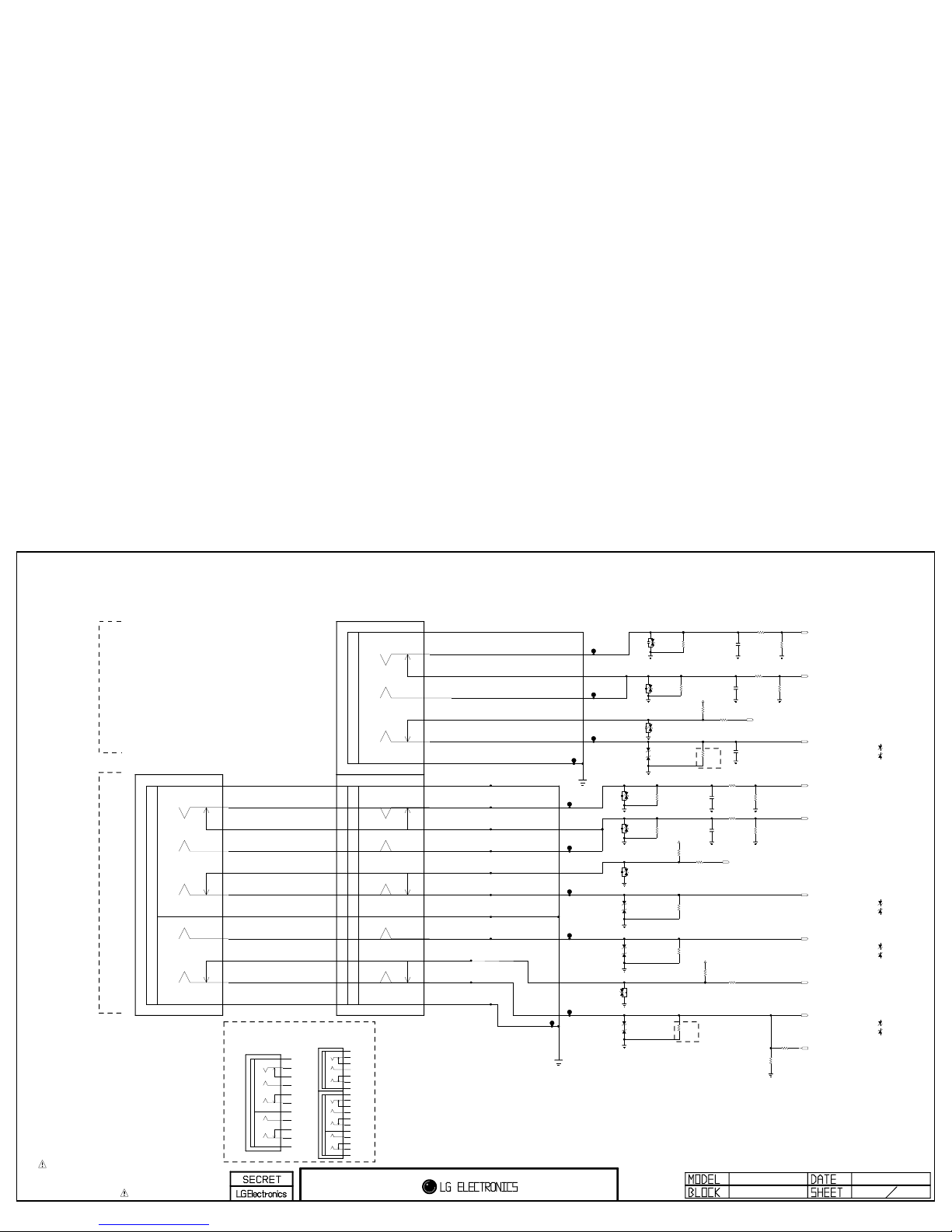
THE SYMBOL MARK OF THIS SCHEMETIC DIAGRAM INCORPORATES
SPECIAL FEATURES IMPORTANT FOR PROTECTION FROM X-RADIATION.
FIRE AND ELECTRICAL SHOCK HAZARDS, WHEN SERVICING IF IS
ESSENTIAL THAT ONLY MANUFACTURES SPECIFIED PARTS BE USED FOR
THE CRITICAL COMPONENTS IN THE SYMBOL MARK OF THE SCHEMETIC.
COMP2_Pr+
AV2_CVBS_DET
R1714
10K
R1721
12K
R1715
10K
R1719
12K
AV2
R1713
1K
R1704
470K
R1700
470K
AV2
VA1702
5.6V
OPT
R1712
1K
COMP2_Pb+
+3.3V_Normal
COMP2_DET
R1701
470K
AV2
R1705
75
R1709
10K
COMP2_R_IN
R1703
470K
VA1703
5.6V
OPT
AV2_R_IN
VA1705
5.6V
OPT
VA1704
5.6V
AV2_LR_ZENER
C1701
1000pF
50V
OPT
R1716
10K
AV2
R1710
10K
C1704
1000pF
50V
OPT
R1706
75
COMP2_L_IN
R1711 1K
AV2
+3.3V_Normal
+3.3V_Normal
VA1700
5.6V
COMP_LR_ZENER
VA1706
5.6V
AV2_LR_ZENER
R1718
12K
AV2
R1708
10K
AV2
SC1/AV2_CVBS_IN
C1703
47pF
50V
AV2
COMP2_Y+/AV_CVBS_IN
C1702
1000pF
50V
OPT
R1720
12K
AV2_L_IN
R1717
10K
AV2
VA1701
5.6V
COMP_LR_ZENER
AV_CVBS_DET
C1705
1000pF
50V
OPT
ZD1704
COMP_Y_ZENER_ROHM
ZD1700
COMP_Pr_ZENER_ROHM
ZD1705
COMP_Y_ZENER_ROHM
ZD1707
AV2_CVBS_ZENER_ROHM
ZD1706
AV2_CVBS_ZENER_ROHM
ZD1703
COMP_Pb_ZENER_ROHM
ZD1702
COMP_Pb_ZENER_ROHM
ZD1701
COMP_Pr_ZENER_ROHM
ZD1707-*1
AV2_CVBS_ZENER_KEC
ZD1706-*1
AV2_CVBS_ZENER_KEC
ZD1703-*1
COMP_Pb_ZENER_KEC
ZD1702-*1
COMP_Pb_ZENER_KEC
ZD1701-*1
COMP_Pr_ZENER_KEC
ZD1700-*1
COMP_Pr_ZENER_KEC
ZD1705-*1
COMP_Y_ZENER_KEC
ZD1704-*1
COMP_Y_ZENER_KEC
R1707
75
1%
1608
R1702
75
1%
AV2
1608
DTV/MNT_VOUT
R1723
75
CVBS_OUT_TEST
R1724
0
CVBS_OUT_TEST
JK1702
PPJ245N2-01
COMP_AV1_YG
5A
[GN/YL]O-SPRING
6A
[GN/YL]E-LUG
4A
[GN/YL]CONTACT
5B
[BL]O-SPRING
7C
[RD1]E-LUG-S
5C
[RD1]O-SPRING
4C
[RD1]CONTACT
5D
[WH]O-SPRING
4E
[RD2]CONTACT
5E
[RD2]O-SPRING
6E
[RD2]E-LUG
JK1702-*1
PPJ245-01
COMP_AV1_G
6A
[GN]C-SPRING
7A
[GN]E-LUG
4A
[GN]CONTACT
5B
[BL]C-SPRING
8C
[RD1]E-LUG-S
6C
[RD1]C-SPRING
4C
[RD1]CONTACT
5D
[WH]C-SPRING
4E
[RD2]CONTACT
6E
[RD2]C-SPRING
7E
[RD2]E-LUG
JK1701-*1
PPJ248-01
COMP_AV1/2_G
6D
[GN]C-SPRING
7D
[GN]E-LUG
4D
[GN]CONTACT
5E
[BL]C-SPRING
8F
[RD1]E-LUG-S
6F
[RD1]C-SPRING
4F
[RD1]CONTACT
5G
[WH1]C-SPRING
4H
[RD2]CONTACT
6H
[RD2]C-SPRING
7H
[RD2]E-LUG
7A
[YL]E-LUG
6A
[YL]C-SPRING
4A
[YL]CONTACT
5B
[WH2]C-SPRING
4C
[RD3]CONTACT
6C
[RD3]C-SPRING
7C
[RD3]E-LUG
JK1701
PPJ248-21
COMP_AV1/2_YG
5D
[YL/GN]O-SPRING
6D
[YL/GN]E-LUG
4D
[YL/GN]CONTACT
5E
[BL]O-SPRING
7F
[RD1]E-LUG-S
5F
[RD1]O-SPRING
4F
[RD1]CONTACT
5G
[WH1]O-SPRING
4H
[RD2]CONTACT
5H
[RD2]O-SPRING
6H
[RD2]E-LUG
6A
[YL]E-LUG
5A
[YL]O-SPRING
4A
[YL]CONTACT
5B
[WH2]O-SPRING
4C
[RD3]CONTACT
5C
[RD3]O-SPRING
6C
[RD3]E-LUG
2013.08.15L14_S7LR(M1A)
REAR_JACK_NON_EU
COMPONENT
&
AV1
17
AV2
COMPONENT & AV1(COMMON), AV2
Size Check !!!
Size Check !!!
* One Ton Color Jack - Yellow/Green
Copyright © 2013 LG Electronics. Inc. All rights reserved.
Only for training and service purposes
LGE Internal Use Only
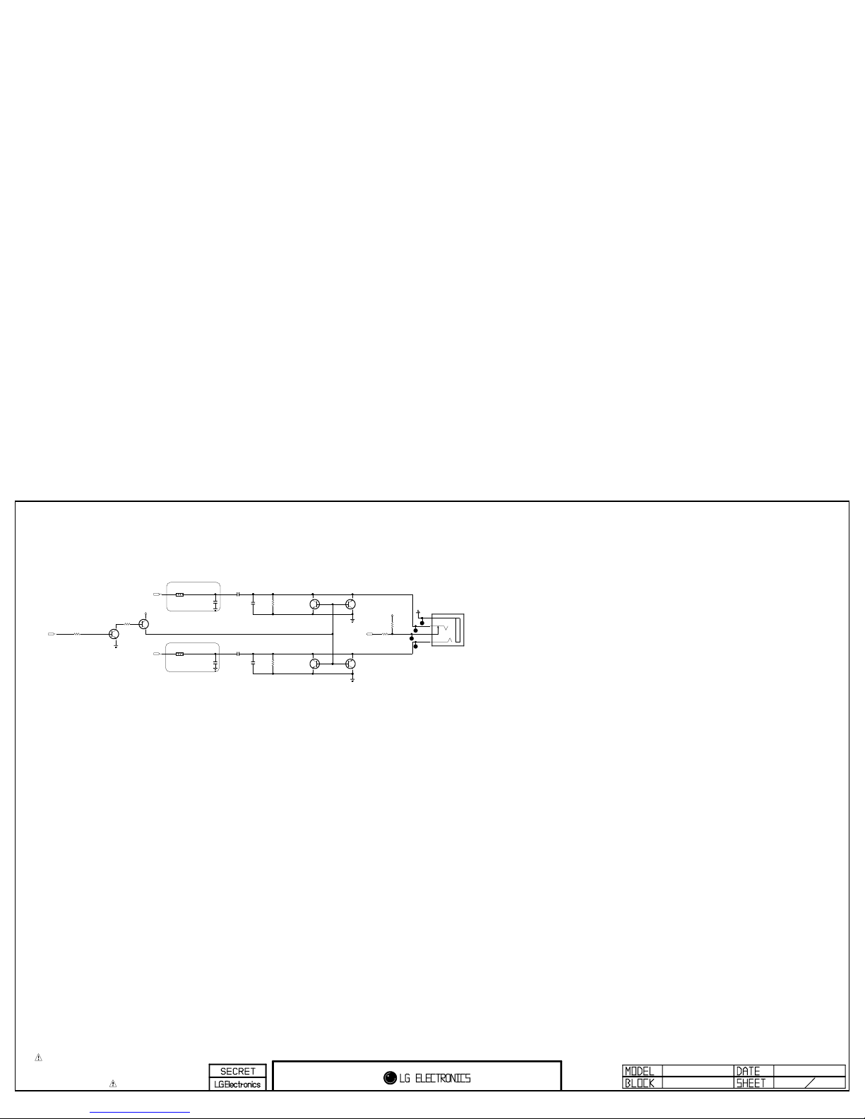
THE SYMBOL MARK OF THIS SCHEMETIC DIAGRAM INCORPORATES
SPECIAL FEATURES IMPORTANT FOR PROTECTION FROM X-RADIATION.
FIRE AND ELECTRICAL SHOCK HAZARDS, WHEN SERVICING IF IS
ESSENTIAL THAT ONLY MANUFACTURES SPECIFIED PARTS BE USED FOR
THE CRITICAL COMPONENTS IN THE SYMBOL MARK OF THE SCHEMETIC.
2013.04.29
HEAD_PHONE_EU 30
NC5_M1A
R3001
3.3K
OPT
C3000
10uF
16V
HEAD_PHONE
C3001
10uF
16V
HEAD_PHONE
JK3000
KJA-PH-0-0177
HEAD_PHONE
3DETECT
4L
5GND
1R
+3.3V_Normal
R3005
10K
HEAD_PHONE
C3003
1000pF
50V
OPT
HP_LOUT
R3004
1K
HEAD_PHONE
HP_DET
+3.5V_ST
HP_ROUT
SIDE_HP_MUTE
R3002
1K
HEAD_PHONE
C3002
1000pF
50V
OPT
R3003
1K
HEAD_PHONE
Q3002
MMBT3904(NXP)
OPT
E
B
C
Q3003
MMBT3904(NXP)
OPT
E
B
C
Q3005
MMBT3904(NXP)
OPT
E
B
C
Q3004
MMBT3904(NXP)
OPT
E
B
C
Q3001
MMBT3906(NXP)
OPT
E
B
C
Q3000
MMBT3904(NXP)
OPT
E
B
C
R3000
1K
OPT
C3004
4.7uF
10V
HEAD_PHONE
L3001
HEAD_PHONE
5.6uH
L3000
HEAD_PHONE
5.6uH
C3005
4.7uF
10V
HEAD_PHONE
Headphone
*Option : HEAD_PHONE_EU
Close to the Main IC
Close to the Main IC
Copyright © 2013 LG Electronics. Inc. All rights reserved.
Only for training and service purposes
LGE Internal Use Only
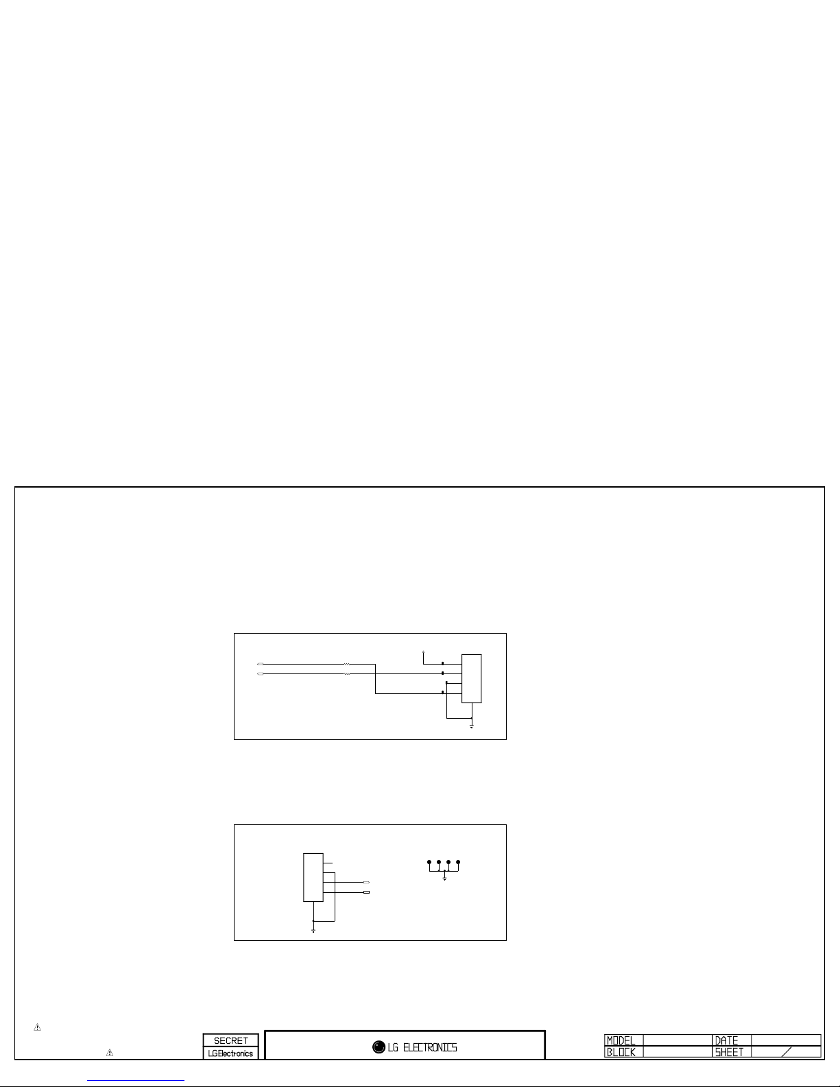
THE SYMBOL MARK OF THIS SCHEMETIC DIAGRAM INCORPORATES
SPECIAL FEATURES IMPORTANT FOR PROTECTION FROM X-RADIATION.
FIRE AND ELECTRICAL SHOCK HAZARDS, WHEN SERVICING IF IS
ESSENTIAL THAT ONLY MANUFACTURES SPECIFIED PARTS BE USED FOR
THE CRITICAL COMPONENTS IN THE SYMBOL MARK OF THE SCHEMETIC.
RS232C_MSTAR_DEBUG_4P
2013/04/30
40
L14_S7LR(M1A)
PM_RXD
+3.5V_ST
R4001
100
R4000
100
P4000
12507WS-04L
RS232C_DEBUG_4P
1
VCC
2
PM_RXD
3
GND
4
RM_TXD
5
GND
PM_TXD
JP_GND3
RGB_DDC_SCL
JP_GND4
RGB_DDC_SDA
JP_GND1
JP_GND2
P4001
12505WS-04A00
MSTAR_DEBUG_4P
1
2
3
4
5
RS-232C 4PIN & MSTAR DEBUG 4PIN
RS-232C 4PIN
MSTAR DEBUG 4PIN
Copyright © 2013 LG Electronics. Inc. All rights reserved.
Only for training and service purposes
LGE Internal Use Only
 Loading...