

Page 1
Internal Use Only
North/Latin America http://aic.lgservice.com
Europe/Africa http://eic.lgservice.com
Asia/Oceania http://biz.lgservice.com
PLASMA TV
SERVICE MANUAL
CHASSIS : PU41A
MODEL : 50PB560B 50PB560B-UA
CAUTION
BEFORE SERVICING THE CHASSIS,
READ THE SAFETY PRECAUTIONS IN THIS MANUAL.
Printed in KoreaP/NO : MFL68001102 (1310-REV00)
Page 2

CONTENTS
CONTENTS .............................................................................................. 2
SAFETY PRECAUTIONS ........................................................................ 3
SPECIFICATION ....................................................................................... 4
ADJUSTMENT INSTRUCTION ................................................................ 5
BLOCK DIAGRAM .................................................................................. 12
EXPLODED VIEW .................................................................................. 13
SCHEMATIC CIRCUIT DIAGRAM ..............................................................
Only for training and service purposes
- 2 -
LGE Internal Use OnlyCopyright © LG Electronics. Inc. All rights reserved.
Page 3
AC Volt-meter
SAFETY PRECAUTIONS
IMPORTANT SAFETY NOTICE
Many electrical and mechanical parts in this chassis have special safety-related characteristics. These parts are identified by in the
Schematic Diagram and Exploded View.
It is essential that these special safety parts should be replaced with the same components as recommended in this manual to prevent
Shock, Fire, or other Hazards.
Do not modify the original design without permission of manufacturer.
General Guidance
An isolation Transformer should always be used during the
servicing of a receiver whose chassis is not isolated from the AC
power line. Use a transformer of adequate power rating as this
protects the technician from accidents resulting in personal injury
from electrical shocks.
It will also protect the receiver and it's components from being
damaged by accidental shorts of th e circuitry that may be
inadvertently introduced during the service operation.
If any fuse (or Fusible Resistor) in this TV receiver is blown,
replace it with the specified.
When replacing a high wattage resistor (Oxide Metal Film Resistor,
over 1 W), keep the resistor 10 mm away from PCB.
Keep wires away from high voltage or high temperature parts.
Before returning the receiver to the customer,
always perform an AC leakage current check on the exposed
metallic parts of the cabinet, such as antennas, terminals, etc., to
be sure the set is safe to operate without damage of electrical
shock.
Leakage Current Cold Check(Antenna Cold Check)
With the instrument AC plug removed from AC source, connect an
electrical jumper across the two AC plug prongs. Place the AC
switch in the on position, connect one lead of ohm-meter to the AC
plug prongs tied together and touch other ohm-meter lead in turn to
each exposed metallic parts such as antenna terminals, phone
jacks, etc.
If the exposed metallic part has a return path to the chassis, the
measured resistance should be between 1 MΩ and 5.2 MΩ.
When the exposed metal has no return path to the chassis the
reading must be infinite.
An other abnormality exists that must be corrected before the
receiver is returned to the customer.
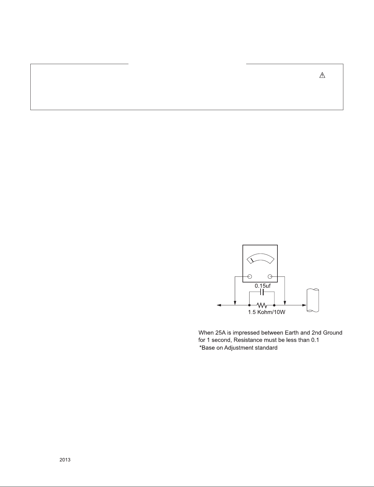
Leakage Current Hot Check (See below Figure)
Plug the AC cord directly into the AC outlet.
Do not use a line Isolation Transformer during this check.
Connect 1.5 K / 10 watt resistor in parallel with a 0.15 uF capacitor
between a known good earth ground (Water Pipe, Conduit, etc.)
and the exposed metallic parts.
Measure the AC voltage across the resistor using AC voltmeter
with 1000 ohms/volt or more sensitivity.
Reverse plug the AC cord into the AC outlet and repeat AC voltage
measurements for each exp ose d metallic par t. Any voltage
measured must not exceed 0.75 volt RMS which is corresponds to
0.5 mA.
In case any measurement is out of the limits specified, there is
possibility of shock hazard and the set must be checked and
repaired before it is returned to the customer.
Leakage Current Hot Check circuit
Good Earth Ground
such as WATER PIPE,
To Instrument's
exposed
METALLIC PARTS
CONDUIT etc.
Only for training and service purposes
- 3 -
LGE Internal Use OnlyCopyright © LG Electronics. Inc. All rights reserved.
Page 4
SPECIFICATION
NOTE : Specifications and others are subject to change without notice for improvement
1. Application range
This spec sheet is applied all of the 42” 50”, 60” PDP TV with PU41A chassis.
2. Requirement for Test
Each part is tested as below without special appointment.
(1) Temperature: 25 °C ± 5 °C(77 °F ± 9 °F), CST: 40 °C ± 5 °C
(2) Relative Humidity: 65 % ± 10 %
(3) Power Voltage
: Standard input voltage (AC 100-240 V~, 50/60 Hz)
* Standard Voltage of each products is marked by models.
(4) Specification and performance of each parts are followed each drawing and specification by part number in accordance with
BOM.
(5) The receiver must be operated for about 5 minutes prior to the adjustment.
3. Test method
(1) Performance: LGE TV test method followed
(2) Demanded other specification
- Safety : CE, IEC specification
- EMC : CE, IEC
.
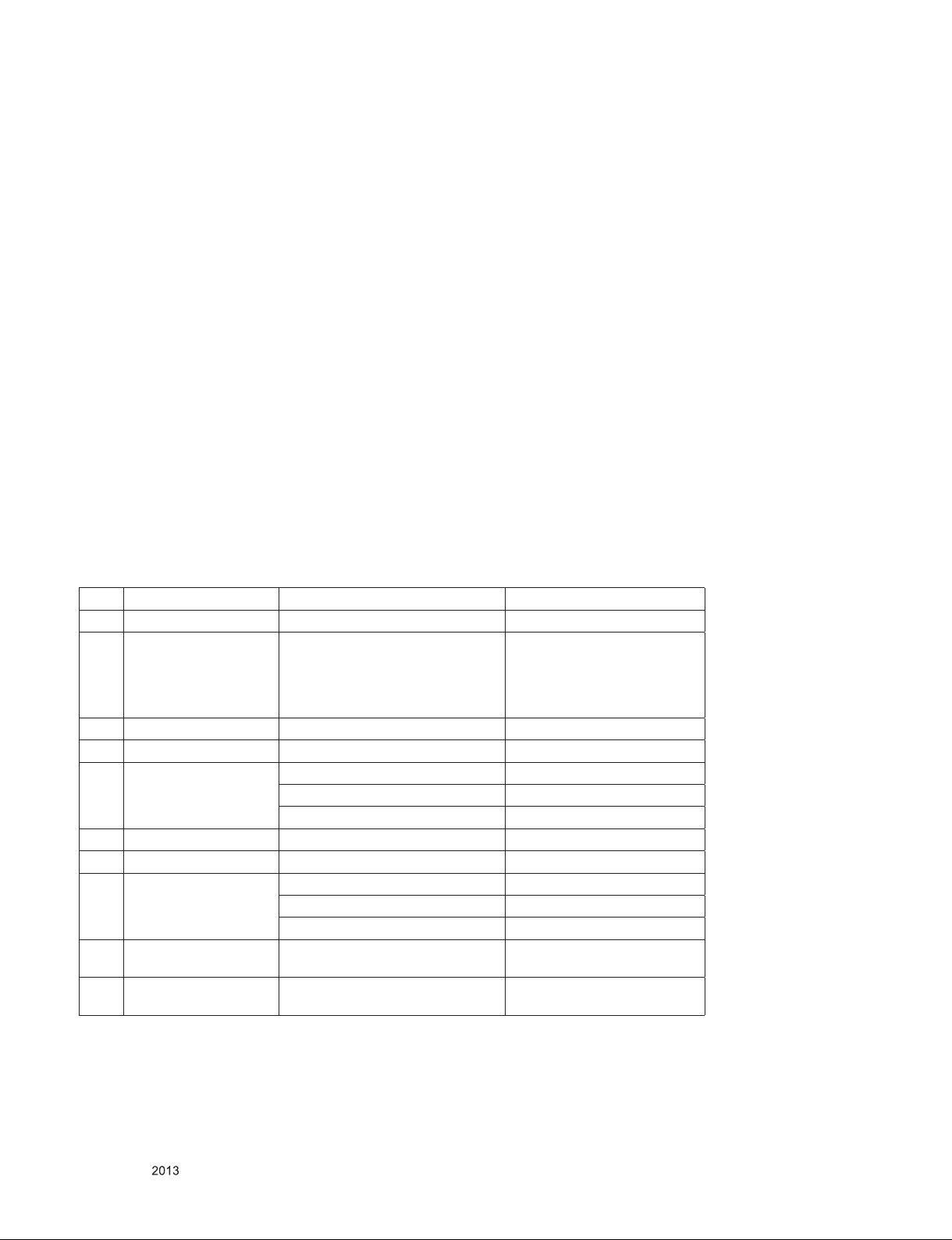
4. Model General Specification
No Item Specication Remark
1 Receiving System 1) ATSC / NTSC-M / 64&256 QAM
2 Available Channel 1) VHF : 02~13
2) UHF : 14~69
3) DTV : 02-69
4) CATV : 01~135
5) CADTV : 01~135
3 Input Voltage 1) AC 110 V, 60 Hz N.America Mark : 110V, 60Hz
4 Market NORTH AMERICA
5 Screen Size 50 inch Wide(1024 × 768) 50PB560B model
50 inch Wide(1920 × 1080) 50PB5600 model
60 inch Wide(1920 × 1080) 60PB5600 model
6 Aspect Ratio 16:9
7 Tuning System FS
8 Module PDP50T6#### (1024 × 768) 50PB560B model
PDP50R6#### (1920 × 1080) 50PB5600 model
PDP60R6#### (1920 × 1080) 60PB5600 model
9 Operating Environment 1) Temp : 0 ~ 40 deg
2) Humidity : ~ 80 %
10 Storage Environment 1) Temp : -20 ~ 60 deg
2) Humidity : ~ 85 %
Only for training and service purposes
- 4 -
LGE Internal Use OnlyCopyright © LG Electronics. Inc. All rights reserved.
Page 5
ADJUSTMENT INSTRUCTION
1. Application Range
This spec. sheet applies to PU41A chassis applied PDP TV all
models manufactured in TV factory.
2. Specification
(1) Because this is not a hot chassis, it is not necessary to
use an isolation transformer. However, the use of isolation
transformer will help protect test instrument.
(2) Adjustment must be done in the correct order. But it is
flexible when its factory local problem occurs.
(3) T he adjustment must be performed in the circumstance of
25 °C ± 5 °C of temperature and 65 % ± 10 % of relative
humidity if there is no specific designation.
(4) The input voltage of the receiver must keep AC 100-220
V~, 50/60 Hz.
(5) Before adjustment, execute Heat-Run for 5 minutes.
■ After Receive 10 0% Full white pattern (06CH) then
process Heat-run
(or “8. Test pattern” condition of Ez-Adjust status)
■ How to make set white pattern
1) Press Power ON button of Service Remocon
2) Press ADJ button of Service remocon. Select “10. Test
pattern” and, after select “White” using navigation
button, and then you can see 100% Full White pattern.
* In this status you can maintain Heat-Run useless any
pattern generator
* Notice: if you maintain one picture over 20 minutes
(Especiall y sharp dis tinction black with white
pattern – 13Ch, or Cross hatch pattern – 09Ch)
then it can appear image stick near black level.
4. PCB Assembly Adjustment
4.1. Using RS-232C
- Adjust 3 items at 3.1. PCB assembly adjustments
" 4.1. ■ Adjustment sequence" one after the order.
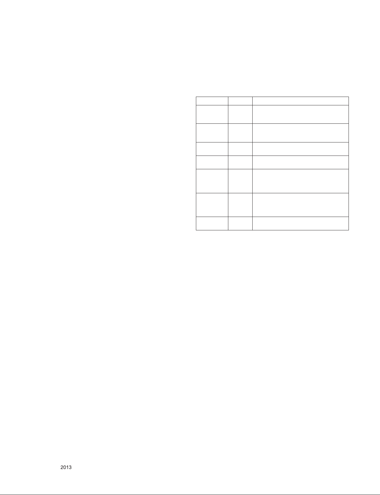
■ Adjustment sequence
Order command Set response
1. Inter the
Adjustment
mode
2. Change
the Source
3. Start
Adjustment
4. Return the
Response
5. Read
Adjustment
data
6. Conrm
Adjustment
7. End of
Adjustment
■ Necessary items before Adjustment items
● Pattern Generator : (MSPG-925FA)
● Adjust 480i comp1
(MSPG-925FA:model :209, pattern :65) - comp1 Mode
● Adjust 1080p comp1
(MSPG-925FA:model :225 , pattern :65) - comp1 Mode
aa 00 00 a 00 OK00x
XB 00 40
XB 00 60
ad 00 10
( main )
ad 00 20
( main )
ad 00 30
ad 00 99 NG 03 00x (Failed condition)
ad 00 90 d 00 OK90x
b 00 OK40x (Adjust 480i Comp1 )
(Adjust 1080p Comp1)
b 00 OK60x (Adjust 1080p RGB)
OKx ( Success condition )
NGx ( Failed condition )
(main : component1 480i, RGB 1080p)
000000000000000000000000007c007b006dx
(main : component1 1080p)
000000070000000000000000007c00830077x
NG 03 01x (Failed condition)
NG 03 02x (Failed condition)
OK 03 03x (Success condition)
< See ADC Adjustment RS232C Protocol_Ver1.0 >
3. Adjustment items
3.1. PCB Assembly adjustment
■ Adjust 480i Comp
■ Adjust 1080p Comp
● If it is necessary, it can adjustment at Manufacture Line
● You can see set adju stm ent status at “9. ADJUST
CHECK” of the “In-start menu”
3.2. Set Assembly Adjustment
■ EDID (The Extended Display Identification Data )
■ Color Temperature (White Balance) Adjustment
■ Make sure RS-232C control
■ Selection Factory output option
Only for training and service purposes
* If you want more information then see the below Adjustment
method (Factory Adjustment)
■ Adjustment sequence
● aa 00 00: Enter the ADc Adjustment mode.
● xb 00 40: change the mode to component1 (No actions)
● ad 00 10: Adjust 480i comp
● ad 00 10: Adjust 1080p comp
● xb 00 90: Endo of Adjustmennt
- 5 -
LGE Internal Use OnlyCopyright © LG Electronics. Inc. All rights reserved.
Page 6
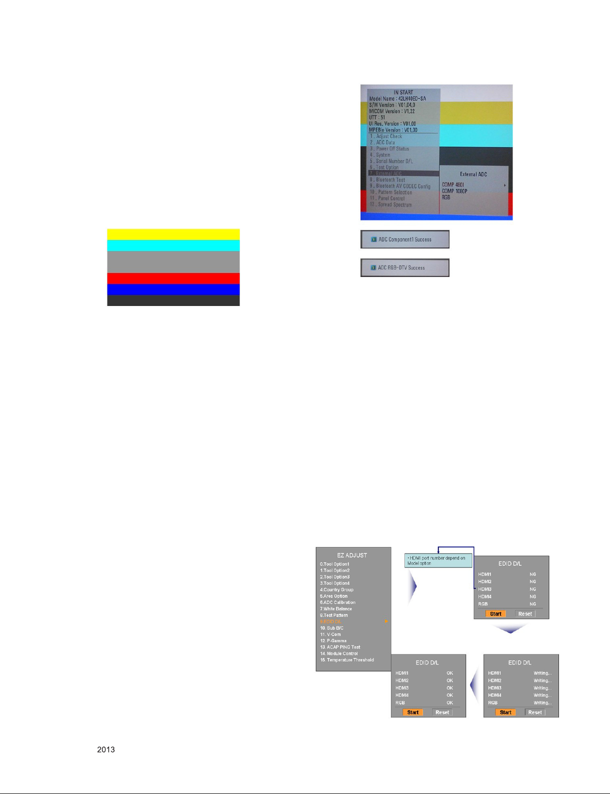
5. Factory Adjustment
-> PU41A : USE INTERNAL ADC(LM1) : using internal pattern.
5.1. Auto Adjust Component 480i/1080p
■ Summary : Adjustment component 480i/1080i is Gain and
Black level setting at Analog to Digital converter,
and compensate the RGB deviation
■ Using instrument
● Adjustment remocon, 801GF(802B, 802F, 802R) or
MSPG925FA pattern generator
( It can output 480i/1080 i horizontal 100% color bar
pa tt ern signal, an d i ts ou tput level must se tt in g
0.7V±0.1V p-p correctly)
< Adjustment pattern : 480i / 1080p 60Hz Pattern >
● You must make it sure its resolution and pattern cause
every instrument can have different setting
● Adjustment method 480i Comp1, Adjust 1080p Comp
(Factory adjustment)
● ADC 480i Component adjustment
- Check connection of Component
- MSPG-925FA -> Model: 209, Pattern 65
● Set Component 480i mode and 100% Horizontal Color
Bar Pattern(HozTV31Bar), then set TV set to Component
mode and its screen to “NORMAL”
● ADC 1080p Component adjustment
- Check connection Component
- MSPG-925FA -> Model: 225, Pattern 65
● Set Component 1080p mode and 100% Horizontal Color
Bar Pattern(HozTV31Bar), then set TV set to Component
mode and its screen to “NORMAL”
● After get each the signal, wait more a second and enter
the “IN-START” with press IN-START key of Service
remocon. After then select “7. External ADC” with
navigator button and press “Enter”.
● After Then Press key of Service remocon “Right Arrow
(VOL+)”
● You can see “ADC Component Success”
● Component1 1080p Adjust is same method.
● Component 1080p Adjustment in Component input mode
* caution : Set Volume 0 after adjustment
5.2. Use Internal ADC(S7R)
- A DJ( E Z ADJ UST ) - > 6.A DC C ali bra tio n - > A DC
Calibration(START)
* EDID (The Extended Display Id entification Data)/DDC
(Display Data Channel) Download.
■ Summary
● It is established in VESA, for communication between
PC and Monitor without order from user for building
user condition. It helps to make easily use realize
“Plug and Play” function.
● For EDID data write, we use DDC2B protocol.
- Auto Download
■ After enter Service Mode by pushing “ADJ” key,
■ Enter EDID D/L mode.
■ Enter “START” by pushing “OK” key.
* Caution:
- Neve r conn ect HD MI & D-sub Cable when the user
downloading .
- Use the proper cables below for EDID Writing
Only for training and service purposes
- 6 -
LGE Internal Use OnlyCopyright © LG Electronics. Inc. All rights reserved.
Page 7
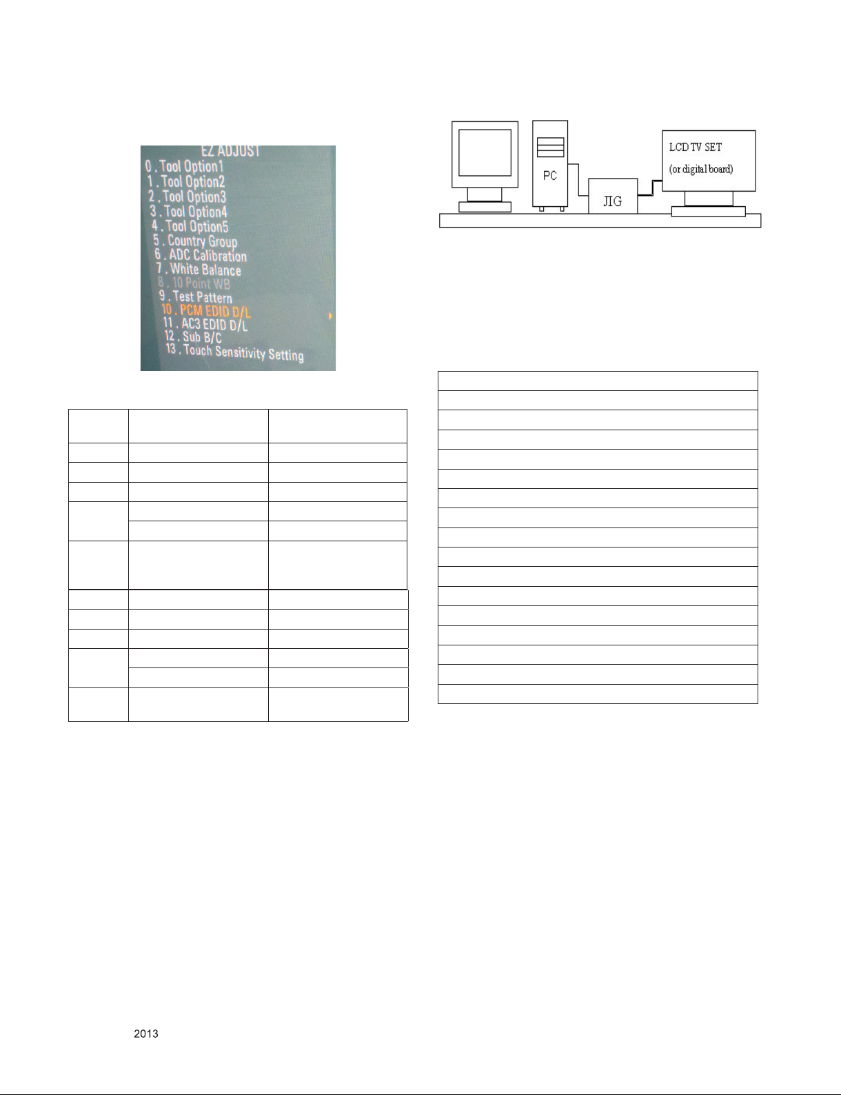
■ It only needs to PCM EDID D/L for North America Product.
(PU41A)
* Edid data and Model option download(RS232)
NO Enter
download MODE
Item download ‘Mode In’ download
CMD 1 A A
CMD 2 E E
Data 0 0 *Note1
0 *Note2
When transfer the
‘Mode In’,
Carry the command.
Item Adjust ‘Mode Out’’ Adjustment Conrmation
CMD 1 A A
CMD 2 E E
Data 0 9 9
0 9
EDID data Model
option download
Automatically download
(The use of a internal
Data)
To check Download
on Assembly line.
< For write EDID data, setting Jig and another instruments >
■ EDID data (Model name = LG TV)
<HD>
-MODEL NAME : 50PB560B
-PCM (C/S : 0x3D, 0x0D)
-HDMI
00 FF FF FF FF FF FF 00 1E 6D 01 00 01 01 01 01
01 18 01 03 80 A0 5A 78 0A EE 91 A3 54 4C 99 26
0F 50 54 A1 08 00 31 40 45 40 61 40 01 01 01 01
01 01 01 01 01 01 64 19 00 40 41 00 26 30 18 88
36 00 B0 84 43 00 00 18 A0 0F 20 00 31 58 1C 20
28 80 14 00 B0 84 43 00 00 1E 00 00 00 FD 00 3A
3E 1E 53 10 00 0A 20 20 20 20 20 20 00 00 00 FC
00 4C 47 20 54 56 0A 20 20 20 20 20 20 20 01 3D
02 03 19 F1 48 10 84 05 02 03 20 22 01 23 09 57
07 67 03 0C 00 10 00 80 2D 01 1D 00 72 51 D0 1E
20 6E 28 55 00 40 84 63 00 00 1E 02 3A 80 18 71
38 2D 40 58 2C 45 00 40 84 63 00 00 1E 01 1D 80
18 71 1C 16 20 58 2C 25 00 40 84 63 00 00 9E 00
00 00 00 00 00 00 00 00 00 00 00 00 00 00 00 00
00 00 00 00 00 00 00 00 00 00 00 00 00 00 00 00
00 00 00 00 00 00 00 00 00 00 00 00 00 00 00 0D
- Manual Download
■ Write HDMI EDID data
● Using instruments
- Jig. (PC Serial to D-Sub connection) for PC, DDC
adjustment.
- S/W for DDC recording (EDID data write and read)
- D-sub jack
- Additional HDMI cable connection Jig.
● Preparing and setting.
- Set instruments and Jig. Like pic.5), then turn on PC
and Jig.
- Operate DDC write S/W (EDID write & read)
- It will operate in the DOS mode.
Only for training and service purposes
- 7 -
LGE Internal Use OnlyCopyright © LG Electronics. Inc. All rights reserved.
Page 8

<HD>
-MODEL NAME : 50PB560B
-AC3 (C/S : 0x3D, 0x9B)
-HDMI
00 FF FF FF FF FF FF 00 1E 6D 01 00 01 01 01 01
01 18 01 03 80 A0 5A 78 0A EE 91 A3 54 4C 99 26
0F 50 54 A1 08 00 31 40 45 40 61 40 01 01 01 01
01 01 01 01 01 01 64 19 00 40 41 00 26 30 18 88
36 00 B0 84 43 00 00 18 A0 0F 20 00 31 58 1C 20
28 80 14 00 B0 84 43 00 00 1E 00 00 00 FD 00 3A
3E 1E 53 10 00 0A 20 20 20 20 20 20 00 00 00 FC
00 4C 47 20 54 56 0A 20 20 20 20 20 20 20 01 3D
02 03 1C F1 48 10 84 05 02 03 20 22 01 26 15 07
50 09 57 07 67 03 0C 00 10 00 80 2D 01 1D 00 72
51 D0 1E 20 6E 28 55 00 40 84 63 00 00 1E 02 3A
80 18 71 38 2D 40 58 2C 45 00 40 84 63 00 00 1E
01 1D 80 18 71 1C 16 20 58 2C 25 00 40 84 63 00
00 9E 00 00 00 00 00 00 00 00 00 00 00 00 00 00
00 00 00 00 00 00 00 00 00 00 00 00 00 00 00 00
00 00 00 00 00 00 00 00 00 00 00 00 00 00 00 9B
- Adjustment Color Temperature(White balance)
■ Using Instruments
● Color Analyzer: CA-210 (CH 10)
- Using LCD color temperature, Color Analyzer (CA-
210) must use CH 10, which Matrix compensated
(White, Red, Green, Blue compensation) with CS-
2100. See the Coordination bellowed one.
● Auto-adjustment Equipment (It needs when Auto-adjustment – It is availed communicate with RS-232C : Baud
rate: 115200)
● Video Signal Generator MSPG-925F 720p, 216Gray
(Model: 217, Pattern 78)
■ Connection Diagram (Auto Adjustment)
● Using Inner Pattern
● Using HDMI input
- See Working Guide if you want more information about EDID
communication.
< connection Diagram for Adjustment White balance >
Only for training and service purposes
- 8 -
LGE Internal Use OnlyCopyright © LG Electronics. Inc. All rights reserved.
Page 9
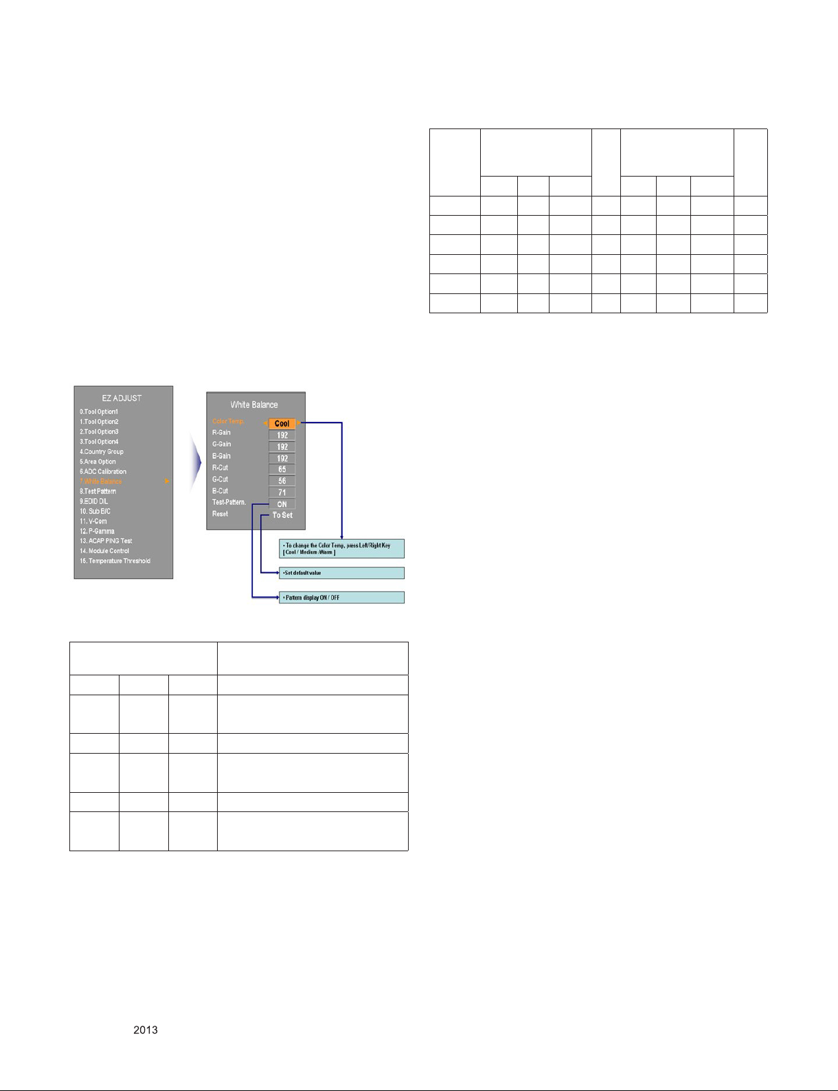
■ White Balance Adjustment
If you can’t adjust with inner pattern, then you can adjust
it using HDMI pattern. You can select option at “Ez-Adjust
Menu – 7. White Balance” there items “NONE, INNER,
HDMI”. It is normally setting at inner basically. If you can’t
adjust using inner pattern you can select HDMI item, and
you can adjust.
In manual Adjust case, if you press ADJ button of service
remocon, and enter “Ez-Adjust Menu – 7. White Balance”,
then automatically inner pattern operates. (In case of
“Inner” originally “Test-Pattern. On” will be selected in The
“Test-Pattern. On/Off”.
● Connect all cables and equipments like Pic.5)
● Set Baud Rate of RS-232C to 115200. It may set 115200
orignally.
● Connect RS-232C cable to set
● Connect HDMI cable to set
■ RS-232C Command (Commonly apply)
RS-232C COMMAND
[CMD ID DATA]
wb 00 00 White Balance adjustment start.
wb 00 10 Start of adjust gain
(Inner white pattern)
wb 00 1f End of gain adjust
wb 00 20 Start of offset adjust
(Inner white pattern)
wb 00 2f End of offset adjust
wb 00 ff End of White Balance adjust
(Inner pattern disappeared)
● “wb 00 00”: Start Auto-adjustment of white balance.
● “wb 00 10”: Start Gain Adjustment (Inner pattern)
● “jb 00 c0” :
● …
● “wb 00 1f”: End of Adjustment
* If it needs, offset adjustment (wb 00 20-start, wb 00 2f-
end)
● “wb 00 ff”: End of white balance adjustment (inner pattern
disappear)
Meaning
■ Adjustment Mapping information
RS-232C
COMMAND
[CMD ID DATA]
Cool Mid Warm Cool Mid Warm
R Gain jg Ja jd 00 184 192 192 192
G Gain jh Jb je 00 187 183 159 192
B Gain ji Jc jf 00 192 161 95 192
R Cut 64 64 64 127
G Cut 64 64 64 127
B Cut 64 64 64 127
● When Color temperature (White balance) Adjustment
(Automatically)
- Press “Power only key” of service remocon and operate
automatically adjustment.
- Set BaudRate to 115200.
● You must start “wb 00 00” and finish it “wb 00 ff”.
● If it needs, then adjustment “Offset”.
■ White Balance Adjustment (Manual adjustment)
● Test Equipment: CA-210
- Using PDP color temperature, Color Analyzer (CA-210)
must use CH 10, which Matrix compensated (White, Red,
Green, Blue compensation) with CS-2100. See the
Coordination bellowed one.
● Manual adjustment sequence is like bellowed one.
- Turn to “Ez-Adjust” mode with press ADJ button of service
remocon.
- Select “10.Test Pattern” with CH+/- button and press
enter. Then set will go on Heat-run mode. Over 30
minutes set let on Heat-run mode.
- Let CA-210 to zero calibration and must has gap more
10cm from center of PDP module when adjustment.
- Press “ADJ” button of service remocon and select
“7.White-Balance” in “Ez-Adjust” then press “►” button of
navigation key. (When press “►” button then set will go to
full white mode)
- Adjust at three mode (Cool, Medium, Warm)
- If “cool” mode
Let B-Gain to 192 and R, G, B-Cut to 64 and then control
R, G gain adjustment High Light adjustment.
- If “Medium” and “Warm” mode Let R-Gain to 192 and R,
G, B-Cut to 64 and then control G, B gain adjustment
High Light adjustment.
- All of the three mode
Let R-Gain to 192 and R, G, B-Cut to 64 and then control
G, B gain adjustment High Light adjustment.
- With volume button (+/-) you can adjust.
- After all adjustment finished, with Enter (■ key) turn to
Ez-Adjust mode. Then with ADJ button, exit from
adjustment mode
* Attachment: White Balance adjustment coordination and
color temperature.
● Using CS-1000 Equipment.
- COOL : T=11000K, ∆uv=0.000, x=0.276 y=0.283
- MEDIUM : T=9300K, ∆uv=0.000, x=0.285 y=0.293
- WARM : T=6500K, ∆uv=0.000, x=0.313 y=0.329
M
I
N
CENTER
(DEFAULT)
M
A
X
Only for training and service purposes
- 9 -
LGE Internal Use OnlyCopyright © LG Electronics. Inc. All rights reserved.
Page 10

● When tester will measure on Cool condition, adjust W30 on
TV display menu.
● When tester will measure on medium condition, adjust 0 on
TV display menu.
● When tester will measure on warm condition, adjust W30 on
TV display menu.
● Using CA-210 Equipment. (10 CH)
- Contrast value: 216 Gray
Color
temperature
COOL CA-210 0.276 ± 0.002 0.283 ± 0.002
MEDIUM CA-210 0.285 ± 0.002 0.293 ± 0.002
WARM CA-210 0.313 ± 0.002 0.329 ± 0.002
- Brightness spec.
Item White average
Min 27.41 -15
Typ 34.55
Max +15
Unit cd/m² %
Remark - 100% Window White
Pattern
- 100IRE(255Gray)
- Picture: Vivid(Medium)
Test
Equipment
brightness
Color Coordination
x y
Brightness uniformity
- 85IRE(216Gray) 100%
Window White Pattern
- Picture: Vivid(Medium)
6. GND and ESD Testing
6.1. Prepare GND and ESD Testing.
■ Check the connection between set and power cord
6.2. Operate GND and ESD auto-test.
■ Fully connected (Between set and power cord) set enter the
Auto-test sequence.
■ Connect D-Jack AV jack test equipment.
■ Turn on Auto-controller(GWS103-4)
■ Start Auto GND test.
■ If its result is NG, then notice with buzzer.
■ If its result is OK, then automatically it turns to ESD Test.
■ Operate ESD test
■ If its result is NG, then notice with buzzer.
■ If its result is OK, then process next steps. Notice it with
Good lamp and STOPER Down.
6.3. Check Items.
■ Test Voltage
● GND: 1.5KV/min at 100mA
● Signal: 3KV/min at 100mA
■ Test time: just 1 second.
■ Test point
● GND test: Test between Power cord GND and Signal
cable metal GND.
● ESD test: Test between Power cord GND and Live and
neutral.
■ Leakage current: Set to 0.5mA(rms)
6.4. POWER PCB Ass’y Voltage adjustment
(Va, Vs voltage adjustment)
6.4.1. Test equipment : : D.M.M 1EA
6.4.2. Connection Diagram for Measuring
: refer to g.1
<XPOWER4 50T5/R5 PSU>
5.3. Test of RS-232C control.
- Press In-Start button of Service Remocon then set the
“4.Baud Rate” to 115200. Then check RS-232C control and
5.4. Selection of Country option.
- Selection of country option is allowed only North American
model (Not allowed Korean model). It is selection of Country
about Rating and Time Zone.
■ Models: All models which PU31A Chassis (See the rst
page.)
■ Press “In-Start” button of Service Remocon, then enter the
“Option” Menu with “PIP CH-“ Button
■ Select one of these three (USA, CANADA, MEXICO) de-
pends on its market using “Vol. +/-“button.
* Caution : Don’t push The INSTOP KEY after completing the
function inspection.
* Caution : Inspection only PAL M / NTSC
Only for training and service purposes
(g.1) PCB Assy Voltage adjustment
6.4.3. Adjustment method
6.4.3.1. Vs adjustment (refer g.1)
(1) Connect + terminal of D.M.M. to Vs pin of P811, connect
-terminal to GND pin of P811
(2) After turning VR901, voltage of D.M.M adjustment as same
as Vs voltage which on label of panel left/top ( deviation ;
±0.5V)
6.4.3.2. Va adjustment (refer g.1)
(1) After receiving 100% Full White Pattern, HEAT RUN.
(2) Connect + terminal of D.M.M. to Va pin of P811, connect
-terminal to GND pin of P811
(3) After turning VR502,voltage of D.M.M adjustment as same
as Va voltage which on label of panel left/top (deviation;
±0.5V)
- 10 -
LGE Internal Use OnlyCopyright © LG Electronics. Inc. All rights reserved.
Page 11
7. Default Service option.
7.1. ADC-Set.
■ R-Gain adjustment Value (default 128)
■ G-Gain adjustment Value (default 128)
■ B-Gain adjustment Value (default 128)
■ R-Offset adjustment Value (default 128)
■ G-Offset adjustment Value (default 128)
■ B-Offset adjustment Value (default 128)
7.2. White balance. Value.
Center(Default)
COOL Mid Warm
R Gain 192 192 192
G Gain 192 192 192
B Gain 192 192 192
R Cut 64 64 64
G Cut 64 64 64
B Cut 64 64 64
7.3. Temperature Threshold
■ Threshold Down Low 20
■ Threshold Up Low 23
■ Threshold Down High 70
■ Threshold Up High 75
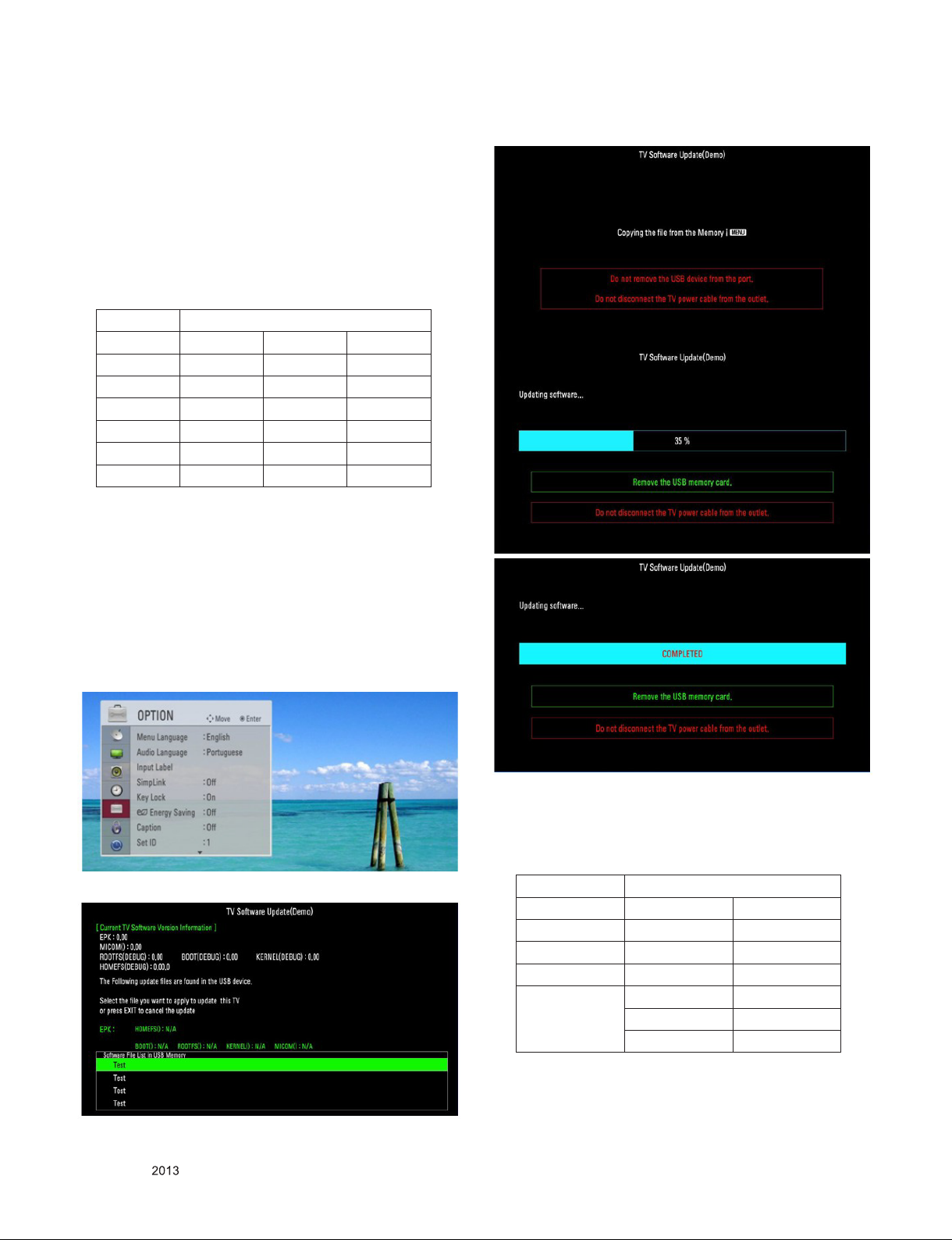
■ Select download le (epk le)
8. USB DOWNLOAD(*.epk le download)
■ Put the USB Stick to the USB socket
■ Press Menu key, and move OPTION
■ Press “FAV” Press 7 times
■ After download is nished, remove the USB stick.
■ Press “IN-START” key of ADJ remote control, check the
S/W version.
9. Tool option
50PB560B-UA
Sffx *US, *CC, *WM *WD
Tool option 1 20740 20740
Tool option 2 1286 1286
Tool option 3 40969 40969
Country US MX
CA
MX
Only for training and service purposes
- 11 -
LGE Internal Use OnlyCopyright © LG Electronics. Inc. All rights reserved.
Page 12
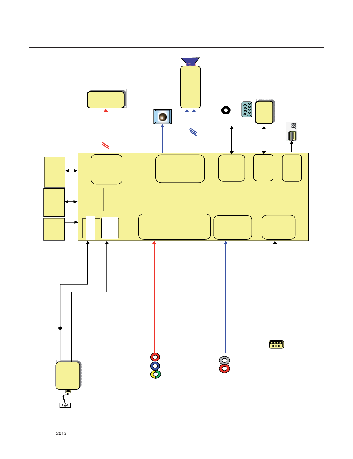
LVDS
Con.HDFHD
BLOCK DIAGRAM
115mV
TAS5733
(Digital AMP)
EEPROM
Serial Flash
X-tal
I2S
MCLK
HD/ FHD
LVDS out
Video
HD/SD
64K x 8bit
Encoder
SPDIF Out
DSP
Audio
RS-232C
RS-232C (Commercial)
RX/TX
MODULE
UART
UART
172mV
DDR2
64Mbit
8M x 8bit
Analog
(24MHz)
DEMOD
Demod
M1L
End
Front
Video
Audio
End
Front
HDMI
Side USB
USB2.0
540mV 420mV
RX
L/R
IF(ATSC)
IF(NTSC)
Y(CVBS)/Cb/Cr
TMDS/DDC
IF
NTSC
/ATSC
Air/Cable
Only for training and service purposes
HDMI (Side)
L/R
(Hybrid)
AV/COMP
- 12 -
AV/COMP/DVI
LGE Internal Use OnlyCopyright © LG Electronics. Inc. All rights reserved.
Page 13
300
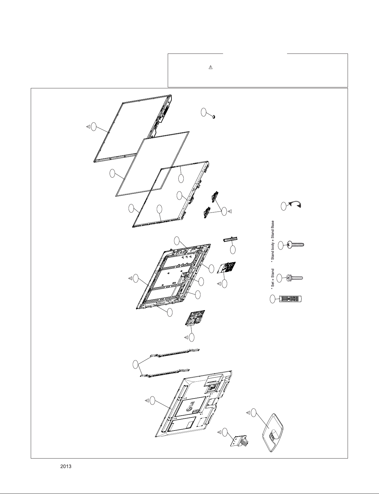
EXPLODED VIEW
IMPORTANT SAFETY NOTICE
Many electrical and mechanical parts in this chassis have special safety-related characteristics. These
parts are identified by in the Schematic Diagram and EXPLODED VIEW.
It is essential that these special safety parts should be replaced with the same components as
recommended in this manual to prevent X-RADIATION, Shock, Fire, or other Hazards.
Do not modify the original design without permission of manufacturer.
560
305
301
200
302
204
205
304
303
580
202
201
120
LV1
A9
601
203
A10
520
A2
Only for training and service purposes
240
400
- 13 -
900
910
LGE Internal Use OnlyCopyright © LG Electronics. Inc. All rights reserved.
Page 14
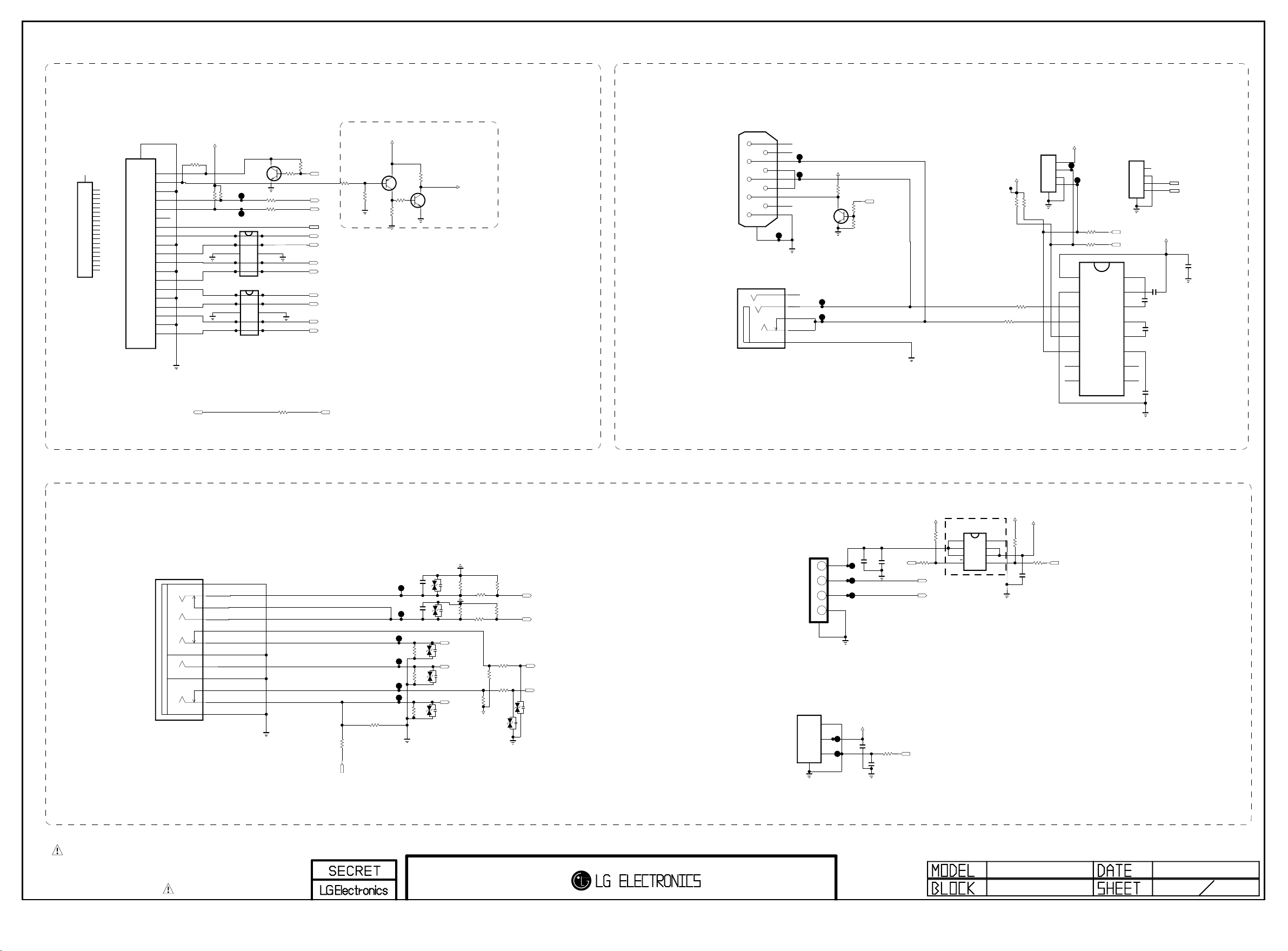
<HDMI>
Copyright © 2013 LG Electronics Inc. All rights reserved.
Only for training and service purposes
LGE Internal Use Only
BODY_SHIELD
20
19
18
17
16
15
14
13
12
11
FHD_Standard
10
9
8
7
6
5
4
3
2
1
JK201-*1
HOT_PLUG_DETECT
VDD[+5V]
DDC/CEC_GND
SDA
SCL
RESERVED
CEC
TMDS_CLK-
TMDS_CLK_SHIELD
TMDS_CLK+
TMDS_DATA0-
TMDS_DATA0_SHIELD
TMDS_DATA0+
TMDS_DATA1-
TMDS_DATA1_SHIELD
TMDS_DATA1+
TMDS_DATA2-
TMDS_DATA2_SHIELD
TMDS_DATA2+
BODY_SHIELD
20
JK201
HDMI_SIDE
For CEC
<RS232C>
<HDMI_SIDE>
JK202
SPG09-DB-009
Commercial
1
6
2
7
3
8
4
9
5
10
RS232C_Phone
JK206
MMBT3904(NXP)
6 M6
1 M1
3 M3_DETECT
4 M4
5 M5_GND
Q201
+5V_ST
C
E
R214
10K
P602
+3.3V_ST
PM_TXD
PM_RXD
1
2
3
4
5
6
7
8
P603
C1+
V+
C1-
C2+
C2-
V-
DOUT2
RIN2
5
1
2
3
4
+3.3V_ST
C228
0.1uF
C225
0.1uF
16V
C226
0.1uF
0.1uF
16V
16V
C227
16V
PM_RXD
PM_TXD
C229
0.1uF
16V
1
2
3
4
5
R283 22
R284 22
VCC
16
GND
15
DOU T1
14
RIN 1
13
ROU T1
12
DIN 1
11
DIN2
10
ROUT2
9
IC206
MAX3232CDR
RS232_Wafer
+3.3V_ST
JP241
R278
IR
R216
100K
B
R217
100K
R276 100
R279
10K
10K
R277
100
R219
10K
Q203
R220
B
4.7K
+3.3V
E
R222
10K
C
C
B
MMBT3904(NXP)
R221
10K
E
5V_DET_HDMI_1
Q204
+5V
JP207
JP208
1
2
3
4
5
1
2
3
4
5
IC201
IC202
MMBT3904(NXP)
C
Q202
E
R231
33
R246
33
10
9
8
7
6
10
9
8
7
6
R268
100
READY
R209
10K
B
R232
10K
HPD1
DDC_SDA_1
DDC_SCL_1
CEC_REMOTE
CK-_HDMI1
CK+_HDMI1
D0-_HDMI1
D0+_HDMI1
D1-_HDMI1
D1+_HDMI1
D2-_HDMI1
D2+_HDMI1
CEC
MMBT3906(NXP)
R218
820
R237
1K
19
18
17
16
15
14
13
12
11
CK+
10
D0-
9
D0_GND
8
D0+
7
D1-
6
D1_GND
5
D1+
4
D2-
3
D2_GND
2
D2+
1
R288
R289
10K
10K
ESD_HDMI_SEMTECH
ESD_HDMI_SEMTECH
CEC_REMOTE
<AV/COMPONENT>
JK210
PPJ234-25
[RD2]FIX
12
[RD2]SWITCH
11
[RD2]SHUNT
10
[WH]SWITCH
9
[RD1]SHUNT
7
[RD1]SWITCH
8
[RD1]EARTH
6
[BL]SWITCH
5
[BL]EARTH
4
[YL/GN]SHUNT
2
[YL/GN]SWITCH
3
[YL/GN]FIX
1
READY
R210
0
CVBS_OUT_TEST
R21 1
75
READY
Close to Main IC
C204
C205
50V
1000pF
50V
1000pF
75
R25 3
75
R25 2
75
R25 1
VA209
VA210
VA208
470 K
R25 5
VA217
470 K
R25 4
VA216
COMP_Pr+
COMP_Pb+
COMP_Y+
R25710K
R256 10K
+3.3V
10K
R259
10K
R265
12K
12K
R262
1K
R267
1K
R266
R263
VA211
COMP_R_IN
COMP_L_IN
COMP_DET
AV_DET
VA212
<SIDE USB>
JK209
1234
USB DOWN STR EAM
5
10mm
<SPDIF>
JK204
GND
1
VCC
2
VINPUT
Fiber Optic
3
4
FIX_POLE
SWITCH ADDED
+3.3V
R264
10K
USB1_OCD
R258
33
SPDIF_OUT
SIDE_USB_DM
SIDE_USB_DP
C213
C212
10uF
0.1uF
10V
16V
+5V
C219
R285
0.1uF
100
16V
C220
10pF
50V
OUT_3
OUT_2
OUT_1
BD82020FVJ
OC
IC204
8
7
6
5
+3.3V
+5V
GND
1
2
3
4
R270
10K
IN_1
READY
IN_2
EN
C201
0.1uF
16V
R271
33
USB1_CTL
THE SYMBOL MARK OF THIS SCHEMETIC DIAGRAM INCORPORATES
SPECIAL FEATURES IMPORTANT FOR PROTECTION FROM X-RADIATION.
FILRE AND ELECTRICAL SHOCK HAZARDS, WHEN SERVICING IF IS
ESSENTIAL THAT ONLY MANUFATURES SPECFIED PARTS BE USED FOR
THE CRITICAL COMPONENTS IN THE SYMBOL MARK OF THE SCHEMETIC.
L13
JACK INTERFACE
2012-06-01
2
7
Page 15
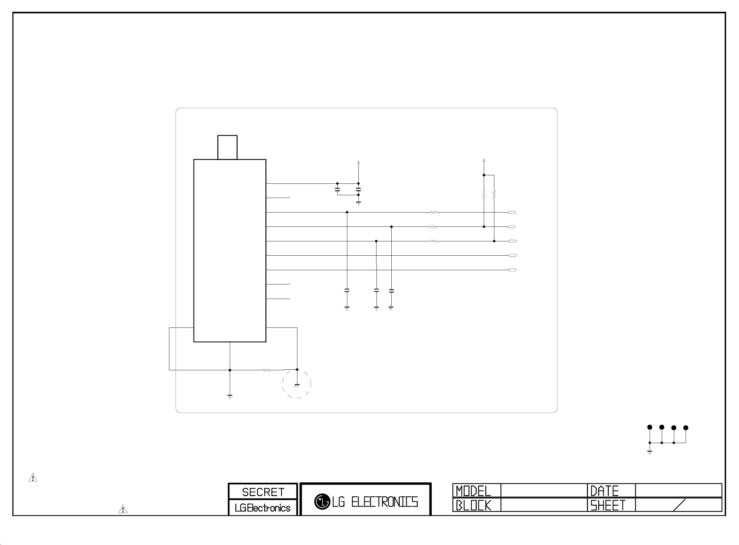
TUNER
Copyright © 2013 LG Electronics Inc. All rights reserved.
Only for training and service purposes
LGE Internal Use Only
14Y TUNER
TU300
A1
A1
47
TDJH-H101F
B1[+3.3V]
1
NC_1
2
IF_AGC
3
SCL
4
SDA
5
IF[P]
6
IF[N]
7
NC_2
8
NC_3
9
B1
B1
C301
0.1uF
16V
+3.3V_TU
READY
16V
0.1uF
C302
10uF
16V
C304
68pF
C303
50V
C305
68pF
50V
+3.3V_TU
R304
1.5K
R30322
R30122
R30222
R305
1.5K
IF_AGC_MAIN
TU_SCL
TU_SDA
IF_P_MSTAR
IF_N_MSTAR
SHIELD
1/16W
R308
READY
5%
0
TU_GND
GND Saparate
THE SYMBOL MARK OF THIS SCHEMETIC DIAGRAM INCORPORATES
SPECIAL FEATURES IMPORTANT FOR PROTECTION FROM X-RADIATION.
FILRE AND ELECTRICAL SHOCK HAZARDS, WHEN SERVICING IF IS
ESSENTIAL THAT ONLY MANUFATURES SPECFIED PARTS BE USED FOR
THE CRITICAL COMPONENTS IN THE SYMBOL MARK OF THE SCHEMETIC.
TUNER
L13
Tuner block
JP653
JP654
JP655
JP656
2012-06-01
3
7
Page 16
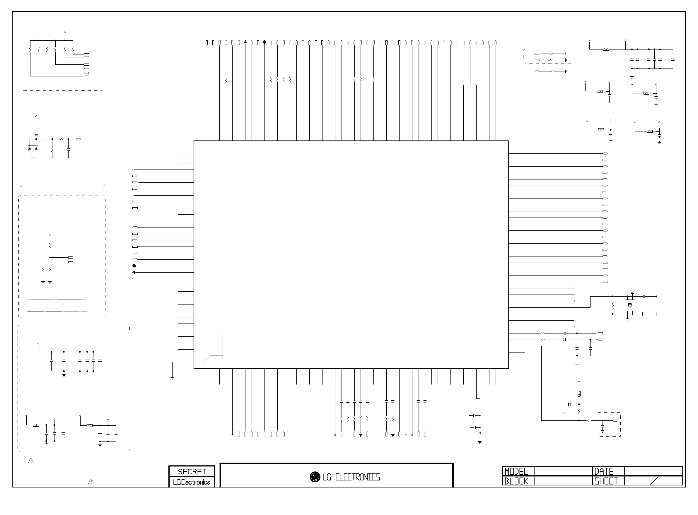
+3.3V
Copyright © 2013 LG Electronics Inc. All rights reserved.
Only for training and service purposes
LGE Internal Use Only
R474
4.7K
R450
4.7K
R451
4.7K
R452
4.7K
R464
4.7K
<SOC_RESET>
+3.3V_ST
C497
D400
10uF
10V
R403
100K
R408
0.1uF
22
C402
<HW_OPT>
+3.3V
FHD
R409 1K
HD
R410 1K
R402 1K
MODEL OPTION
PIN NAME
MODEL_OPT_1
MODEL_OPT_2
LOW
FHD
<VDDC 1.15V>
+1.15V_VDDC
10uFC455
<SY-BY Power 3.3V>
L401
AVDD_DADC
C401
0.1uF
AVDD_AU33
C408
0.1uF
RXA4+
RXA4-
RXA3+
RXA3-
RXACK+
RXACK-
RXA2+
RXA2-
RXA1+
RXA1-
RXA0+
RXA0-
AUD_LRCH
AUD_SCK
AUD_MASTER_CLK
AUD_LRCK
SPDIF_OUT
5V_DET_HDMI_1
MODEL_OPT2
MODULE_UART_RXD
MODULE_UART_TXD
R447
IF_N_MSTAR
IF_P_MSTAR
AVDD_MOD
1uFC435
10uFC434
+3.3V_ST
+3.3V_ST
C451 10pF
1
X-TAL_12GND_1
1M
GND_2
4
24MHz
X400
3
X-TAL_2
C452 10pF
C438 0.1uF
AVDD_DMPLL
L403
L406
C440 0.1uF
C441 0.1uF
C409
0.1uF
AVDD_VIDEO
C407
0.1uF
C445 0.1uF
P_AMP_SCL
PWM1
AC_DET
IR
SOC_RESET
SIDE_USB_DP
SIDE_USB_DM
R453
4.7K
LCD(NOT USE)PDP
C467 1uF
MODEL_OPT1
MODEL_OPT2
HIGH
HD
0.1uF
C474
I2C_SDA
I2C_SCL
P_AMP_SDA
P_AMP_SCL
MODULE_UART_RXD
MODULE_UART_TXD
SOC_RESET
0.1uF
0.1uF
C480
C478
C482 0.1uF
AVDD_MOD
KEY1
KEY2
17V_VS_DET
+1.15V_VDDC
DDR_DATA
MODEL_OPT1
DDC_SCL_1
DDC_SDA_1
AV_DET
EYE_SDA
EYE_SCL
COMP_DET
+1.15V_VDDC
RESET
DM_P0
DP_P0
122
123
DM_P1
DP_P1
AVDD_MOD_4
SAR0/GPIO75
SAR1/GPIO74
SAR2/GPIO73
VDDC_3
VDDIO_DATA
GPIO54
DDCDD_CL
DDCDD_DA
DDCDA_CL
DDCDA_DA
MHL_DET/GPIO86
DDCDB_DA
DDCDB_CL
HOTPLUG_B
TP4
AVDD_5V_MHL
GND_EFUSE
VDDC_4
RXCN_D
RXCP_D
RX0N_D
RX0P_D
RX1N_D
RX1P_D
RX2N_D
RX2P_D
RXCN_B
RXCP_B
RX0N_B
RX0P_B
E-PAD
125
126
127
128
129
130
131
132
133
134
135
136
137
138
139
140
141
142
143
144
145
146
147
148
149
150
151
152
153
154
155
156
124
157
THERMAL
1
CEC
PM_RXD
R421
100
DDCA_CK
TEST
CEC
IRIN
INT/GPIO64/I2S_OUT_MCK
117
118
119
120
121
5
6
SPI_SCK
/SPI_CS
SPI_SDI
SPI_SDO
R401 33
R413 33
PWM0/GPIO15
SPI_DO
SPI_DI
111
112
PWM0
110
TP5
PM_TXD
33
R414 33
R407
Don’t use arc/gpio87 as GPIO
SPI_CZ
SPI_CK
ARC/GPIO87
DDCA_DA
113
114
115
116
LGE8220(MSD8220LBM)
15
AMP_MUTE
HPD1
I2C_SCL
GPIO0/TCON0
HOTPLUG_D
HOTPLUG_A
PWM1/GPIO14
106
107
108
109
16
17
LED_RED
DISP_EN
AMP_RESET_N
I2C_SDA
GPIO5/TCON5
GPIO4/TCON4
GPIO3/TCON3
GPIO2/TCON2
GPIO1/TCON1
102
103
104
105
IC400
[M1L]
20
21
22
23
/FLASH_WP
RL_ON
VS_ON
R415
R416
R417
100
100
100
GPIO8/TCON8
GPIO7/TCON7
GPIO6/TCON6
98
99
100
101
24
27
5V_ON
TU_SCL
GPIO9/TCON9
97
28
P_AMP_SDA
USB1_CTL
TU_SDA
LVSYNC/GPIO16/RLV0-/GPIO16
GPIO10/TCON10
95
96
30
USB1_OCD
RXB4+
R_ODD[7]/LVB0-/RLV2-/EPI7-
LCK/GPIO19/RLV1+/GPIO19
LDE/GPIO18/RLV1-/GPIO18
LHSYNC/GPIO17/RLV0+/GPIO17
91
92
93
94
31
32
33
34
RXB3-
RXB3+
RXB4-
R_ODD[6]/LVB0+/RLV2+/EPI7+
90
AVDD_MOD
AVDD_MOD_3
R_ODD[4]/LVB1+/RLV3(CLK)+/EPI6+
R_ODD[5]/LVB1-/RLV3(CLK)-/EPI6-
87
88
89
RXBCK+
RXBCK-
R_ODD[2]/LVB2+/RLV4+/EPI5+
R_ODD[3]/LVB2-/RLV4-/EPI5-
85
86
RXB1+
RXB2+
RXB2-
G_ODD[7]/LVB3-/RLV6-/EPI3-
R_ODD[0]/LVBCLK+/RLV5+/EPI4+
R_ODD[1]/LVBCLK-/RLV5-/EPI4-
82
83
84
42
RXB0-
RXB1-
RXB0+
G_ODD[4]/LVB4+/LLV0+/EPI2+
G_ODD[5]/LVB4-/LLV0-/EPI2-
G_ODD[6]/LVB3+/RLV6+/EPI3+
79
80
81
44
45
G_ODD[3]/LVA0-/LLV1-/EPI1-
78
G_ODD[2]/LVA0+/LLV1+/EPI1+
77
G_ODD[1]/LVA1-/LLV2-/EPI0-
76
G_ODD[0]/LVA1+/LLV2+/EPI0+
75
B_ODD[7]/LVA2-/LLV3(CLK)-
74
B_ODD[6]/LVA2+/LLV3(CLK)+
73
B_ODD[5]/LVACLK-/LLV4-
72
B_ODD[4]/LVACLK+/LLV4+
71
B_ODD[3]/LVA3-/LLV5-
70
B_ODD[2]/LVA3+/LLV5+
69
B_ODD[1]/LVA4-/LLV6-
68
B_ODD[0]/LVA4+/LLV6+
67
GPIO53/I2S_OUT_SD
66
GPIO52/I2S_OUT_BCK
65
GPIO51/I2S_OUT_MCK
64
GPIO50/I2S_OUT_WS
63
GPIO49/SPDIF_OUT
62
GPIO47
61
GPIO46/MHL_VBUS
60
GPIO45/I2C_SCLM/UART_RX1
59
GPIO44/I2C_SDAM/UART_TX1
58
VDDC_2
57
VDDIO_CMD
56
AVDD_MOD_2
55
XOUT
54
XIN
53
AVDD3P3_DMPLL
52
AVDD3P3_DADC
51
VIFM
50
VIFP
49
IFAGC
48
LINEOUTR0
47
46
Chip config
PWM1
PWM0
DISP_EN
R459 1K
R461 1K
R411 1K
R465
0
R466
0
Close to MSTAR
C462
C461
0.1uF
0.1uF
+3.3V_ST
+3.3V_ST
+3.3V_ST
+1.15V_VDDC
DDR_CMD
AVDD_MOD
AVDD_DMPLL
AVDD_DADC
READY
C464
100pF
DTV_IF
READY
C463
100pF
L400
L405
<DDR 1.8V>
+1.8V_DDR
L402
C436
DDR_CMD
C442
10uF
THE SYMBOL MARK OF THIS SCHEMETIC DIAGRAM INCORPORATES
SPECIAL FEATURES IMPORTANT FOR PROTECTION FROM X-RADIATION.
FILRE AND ELECTRICAL SHOCK HAZARDS, WHEN SERVICING IF IS
ESSENTIAL THAT ONLY MANUFATURES SPECFIED PARTS BE USED FOR
THE CRITICAL COMPONENTS IN THE SYMBOL MARK OF THE SCHEMETIC.
0.1uF
C403
10uF
+1.8V_DDR
L404
C414
DDR_DATA
C410
10uF
0.1uF
C404
10uF
RX1N_B2RX1P_B3RX2N_B4RX2P_B
AVDD_MOD_1
AVDD_MOD
D2-_HDMI1
D2+_HDMI1
BIN0P
RXCN_A7RXCP_A8RX0N_A9RX0P_A10RX1N_A11RX1P_A12RX2N_A13RX2P_A14HSYNC0
D0-_HDMI1
D0+_HDMI1
D1-_HDMI1
D1+_HDMI1
CK+_HDMI1
CK-_HDMI1
GIN0P18GIN0M19RIN0P
SOGIN0
BIN1P
VSYNC0
SOGIN1
AVDD3P3_ADC
C439 0.047uF
R434 33
COMP_Pb+
AVDD_VIDEO
GIN1P25GIN1M26RIN1P
C443 1000pF
C433 0.047uF
C430 0.047uF
R446 33
R445 68
R443 33
COMP_Y+
VSYNC1
0.047uF
C429
R444 33
COMP_Pr+
VCOM
CVBS129CVBS0
C449 0.047uF
C413 0.047uF
R426 150
R427 180
COMP_Y+
AUR035AUL036AUR137AUL138AUR239AUL240AUR341AUL3
VDDC_1
CVBS_OUT1
AVDD_AU33
AVDD_AU33
+1.15V_VDDC
CVBS_OUT_TEST
C4062.2uF
2.2uF
COMP_R_IN
COMP_L_IN
C405
VAG43VRM
C411
0.1uF
C412
10uF
LINEOUTL3
LINEOUTR3
LINEOUTL0
L408
BLM18PG121SN1D
L13
MAIN
C468
0.1uF
+3.3V
L410
R469
10K
NON_A_DEMODE
AGC 1.25V
100 OHM SERIAL
BLM18PG121SN1D
A_DEMODE 0ohm
100
R471
Close to MSTAR
C469
0.047uF
25V
IF_AGC_MAIN
2012-06-201
4
7
Page 17
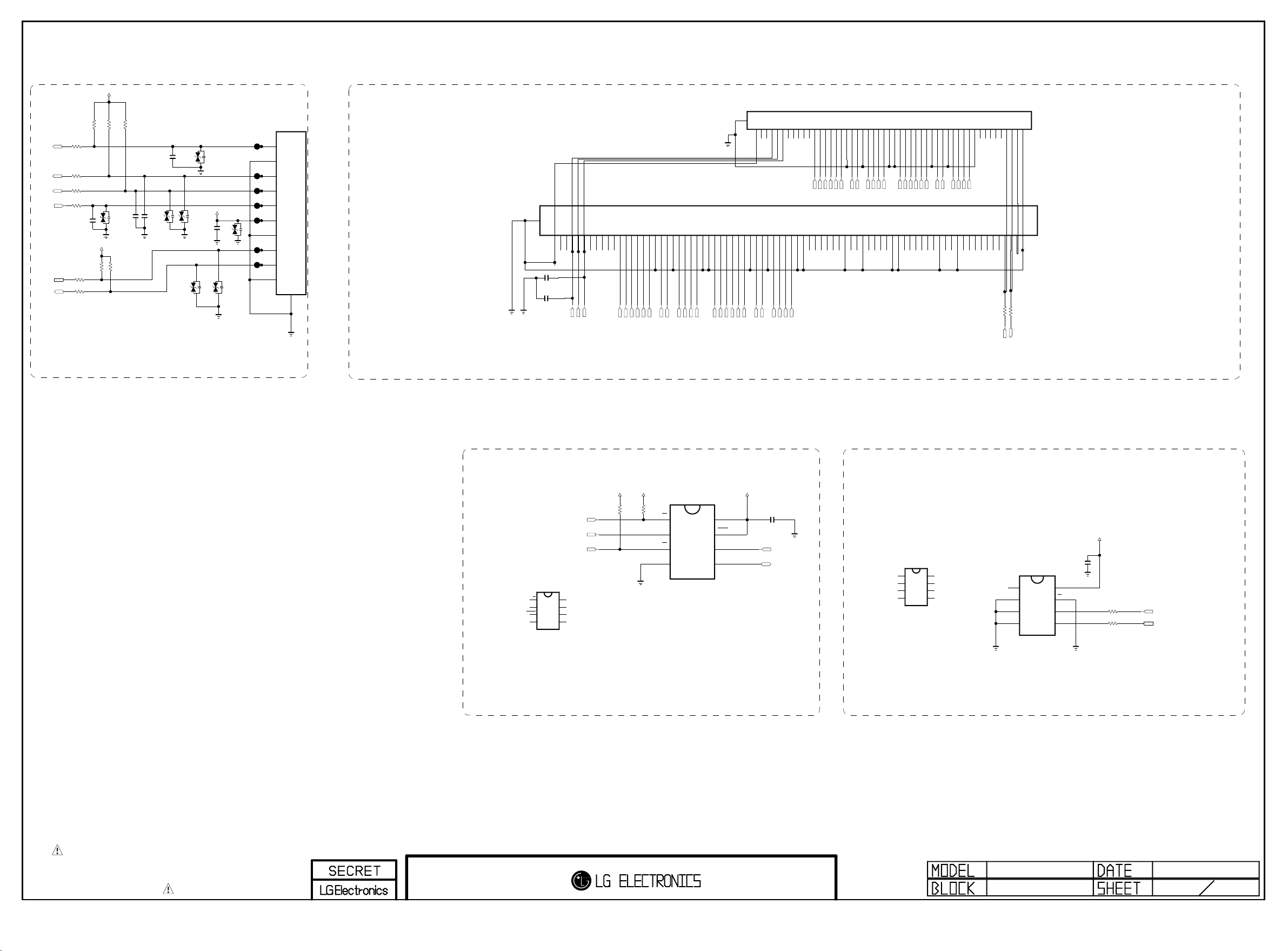
<KEY/IR>
Copyright © 2013 LG Electronics Inc. All rights reserved.
Only for training and service purposes
LGE Internal Use Only
+3.3V_ST
<LVDS>
KEY1
KEY2
LED_RED
EYE_SDA
EYE_SCL
R529
R527
Commercial
R521
100
IR
R522
100
R523
100
R524
22
C520
10pF
50V
+3.3V
R5281KR530
R525
100
R526
100
4.7K
READY
1K
10K
D501
R531
C521
0.1uF
20V
10K
C523
10pF
50V
C522
0.1uF
16V
16V
READY
20V
D500
READY
+3.3V_ST
C524
D502 20V
D503 20V
READY
0.1uF
READY
16V
READY
D505 20V
20V
D504
READY
D506 20V
P501
12507WR-10L
1
2
3
4
5
6
7
8
9
10
11
81
470pF
READY
470pF
READY
C518
C519
DISP_EN
P_AMP_SCL
P_AMP_SDA
RXB4+
RXB4-
RXB3+
RXB3-
RXBCK-
RXBCK+
RXB2+
RXB2-
RXB1+
RXB1-
RXB0+
RXB0-
RXA4+
RXA4-
RXA3+
RXA3-
RXACK+
RXACK-
52
48
495051
HD
16
17181920212223242526272829303132333435363738394041424344454647
123456789101112131415
P503
TF05-51S
RXB4-
FHD
RXB4+
RXB3+
RXB3-
RXBCK-
RXBCK+
RXB2+
RXB2-
RXB1+
RXB1-
RXB0+
26272829303132333435363738394041424344454647484950515253545556575859606162636465666768697071727374757677787980
RXB0-
RXA4-
RXA2+
RXA3+
RXA4+
RXACK+
RXA3-
232425
RXACK-
RXA1-
RXA0-
RXA1+
RXA2-
RXA0+
P500
16171819202122
8
9101112131415
1234567
104060-8017
R520
R519
22
22
RXA1-
RXA0-
RXA1+
RXA2+
RXA0+
RXA2-
* LCI: LVDS Connection Indicator
MODULE_UART_RXD
MODULE_UART_TXD
<SERIAL FLASH>
/SPI_CS
SPI_SDO
/FLASH_WP
Winbond
IC505-*1
W25Q64FVSSIG
VCC
CS
8
1
DO[IO1]
WP[IO2]
%HOLD[IO3]
7
2
CLK
6
3
GND
DI[IO0]
4
5
+3.3V_ST
R564
10K
+3.3V_ST
MX25L6406EM2I-12G
R569
4.7K
READY
SO/SIO1
GND
<NVRAM>
8
7
6
5
VCC
HOLD
SCLK
SI/SIO0
+3.3V_ST
C556
0.1uF
SPI_SCK
SPI_SDI
ATMEL
IC503-*1
AT24C512C-SSHD-T
A0
1
A1
2
A2
3
GND
4
+3.3V
C552
ST
VCC
8
WP
7
SCL
6
SDA
5
IC503
M24512-RMN6TP
E0
1
E1
2
E2
3
VSS
4
0.1uF
VCC
8
WC
7
SCL
6
SDA
5
R573
22
R574
22
I2C_SCL
I2C_SDA
MX
IC505
CS
1
2
WP
3
4
THE SYMBOL MARK OF THIS SCHEMETIC DIAGRAM INCORPORATES
SPECIAL FEATURES IMPORTANT FOR PROTECTION FROM X-RADIATION.
FILRE AND ELECTRICAL SHOCK HAZARDS, WHEN SERVICING IF IS
ESSENTIAL THAT ONLY MANUFATURES SPECFIED PARTS BE USED FOR
THE CRITICAL COMPONENTS IN THE SYMBOL MARK OF THE SCHEMETIC.
L13
Memory.LVDS,IR
2012-06-01
5
7
Page 18
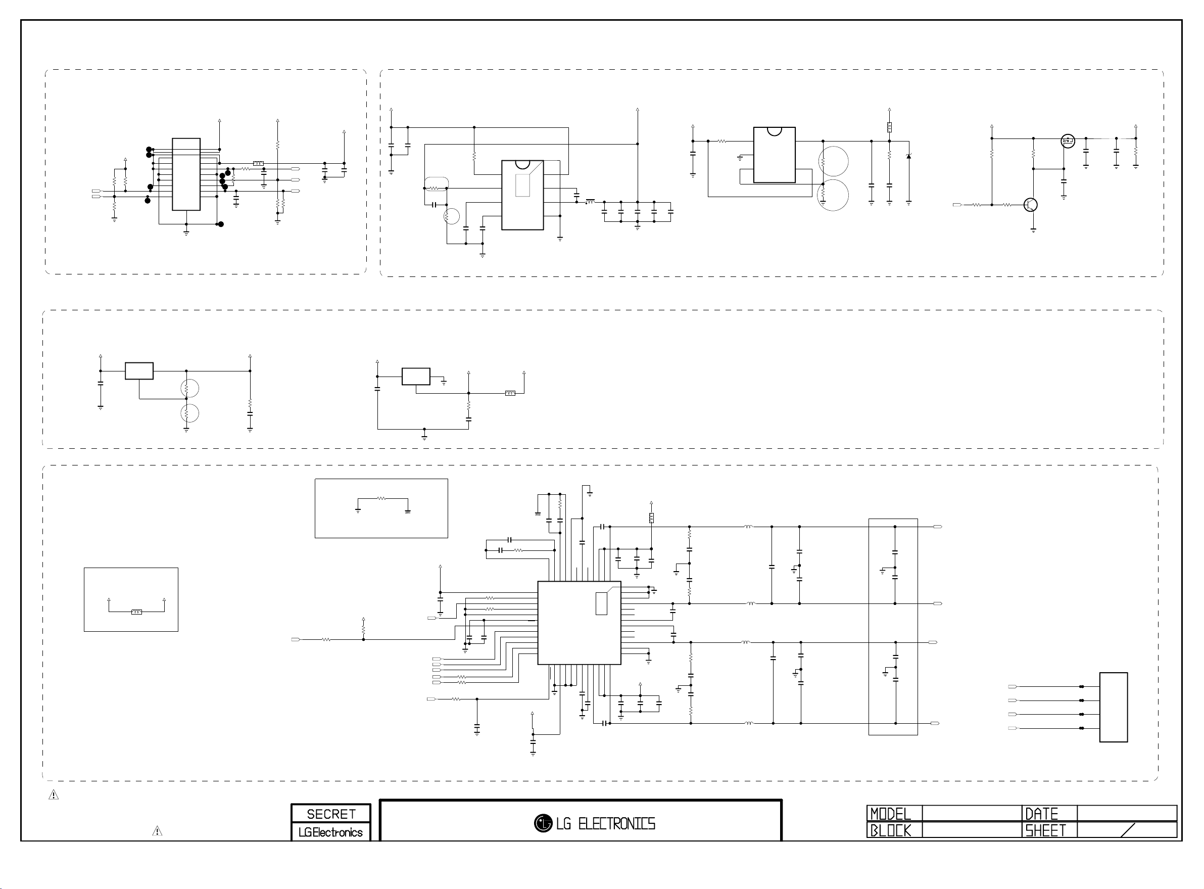
POWER & AMP
Copyright © 2013 LG Electronics Inc. All rights reserved.
Only for training and service purposes
LGE Internal Use Only
<ST-BY>
<Power Wafer>
+3.3V_ST
R601
R600
10K
10K
READY
RL_ON
5V_ON
4.7K
R604
<MUTI>
+1.8V_DDR
+5V
AZ1117EH-ADJTRG1
C618
10uF
10V
IC613
ADJ/GND
P600
SMAW200-H18S1
1
3
5
7
9
10
12
11
14
13
16
15
18
17
19
+5V_ST --> 3.3Vst
C601
0.1uF
16V
+3.3V_ST
120
L604
R608
1
SIGN900778
C604
10uF
10V
+5V_ST
P_17V
2
4
6
8
0
R612
R609
C607
0.1uF
16V
+3.3V_ST
+5V_ST
C621
C620
0.1uF
10uF
50V
R624
12K
READY
L600
120
C606
100
0.1uF
16V
10K
R606
4.7K
R639
17V_VS_DET
VS_ON
AC_DET
C608
10uF
10V
C610
0.1uF
16V
25V
R617
27K
1%
C623
100pF
50V
R1
R619
51K
1%
R607
10K
R2
C624
1uF
10V
VREG5
C626
3300pF
50V
EN
VFB
SS
IC603
TPS54327DDAR
1
9
2
THERMAL
3
3A
4
8
7
6
5
[EP]GND
VIN
VBST
SW
GND
C628
0.1uF
L605
16V
2.2uH
+1.15V_VDDC
C650
10uF
16V
C629
10uF
16V
C630
0.1uF
16V
C611
10uF
16V
C612
10uF
16V
+5V_ST
C600
1uF
25V
R602
3.3K
ADJ/NC
GND
EN
IC600
AP7361-Y-13
1
2
3
Vo=0.8*(1+R1/R2)
OUT
5
R603
10K
IN
4
1%
R605
3.3K
1%
R1
R2
D600
5V_STBY --> MULTI 5V1.15V Core
C605
0.1uF
16V
+5V
R671
10K
READY
+5V_ST
R657
10K
R610
0
READY
R659
10K
B
5V
RL_ON
3A
R664
10K
C
Q603
MMBT3904(NXP)
E
Q604
DMP2130L
S
G
READY
C602
2.2uF
10V
D
C603
0.1uF
16V
READY
Vout=0.765*(1+R1/R2)
+5V->+3.3V
+1.8V_DDR
OUTIN
R1
1%
220
R674
R2
1%
100
R673
R675
1
C619
10uF
10V
->+3.3V_TU
+5V
C616
10uF
10V
IC608
AP1117E33G-13
IN ADJ/GND
OUT
+3.3V
R662
1
C617
10uF
6.3V
L606
120-ohm
2A
+3.3V_TU
<AUDIO AMP>
+3.3V
L601
BLM18PG121SN1D
Vout=1.25*(1+R2/R1)
+3.3V_AMP
AMP_MUTE
R611
0
Separate DGND AND AVSS
+3.3V_AMP
R626
R627
33
4.7K
AUD_MASTER_CLK
AUD_LRCK
AUD_SCK
AUD_LRCH
P_AMP_SDA
P_AMP_SCL
AMP_RESET_N
+3.3V_AMP
C636
0.1uF
16V
This parts are Located
on AVSS area.
C641
C640
0.047uF
R632 15K
A_SEL_FAULT
18K
1%
R631
C637
C639
4.7uF
0.1uF
10V
33 R629
R63033
R62833
C638
0.1uF
16V
4700pF
R633
470
OSC_RES
AVDD
MCLK
DVSSO
VR_DIG
PDN
LRCLK
SCLK
SDIN
SDA
SCL
+3.3V_AMP
C642
0.1uF
16V
C651
0.1uF
50V
[EP]
PGND_AB_2
PGND_AB_1
OUT_B
NC_6
NC_5
BST_B
BST_C
NC_4
NC_3
OUT_C
PGND_CD_2
PGND_CD_1
C652
0.1uF
50V
P_17V
C653
10uF
35V
C654
10uF
35V
P_17V
L602
CIS21J121
READY
C655
10uF
35V
READY
C656
10uF
35V
50V
0.033uF
C657
50V
0.033uF
C658
R635
18
C659
330pF
50V
C660
330pF
50V
R636
18
R637181/16W
C661
330pF
50V
C662
330pF
50V
R638181/16W
NRS6045T100MMGK
L610
10.0uH
L612
10.0uH
NRS6045T100MMGK
NRS6045T100MMGK
L609
10.0uH
L611
10.0uH
NRS6045T100MMGK
C663
0.47uF
50V
C664
0.47uF
50V
C665
0.1uF
50V
C666
0.1uF
50V
C667
0.1uF
50V
C668
0.1uF
50V
Close to Speaker
C669
2200pF
50V
C670
2200pF
50V
C671
2200pF
50V
C672
2200pF
50V
SPK_L+
SPEAKER_L
SPK_L-
SPK_R+
SPEAKER_R
SPK_R-
SPK_L+
SPK_L-
SPK_R+
SPK_R-
P601
WAFER-ANGLE
4
3
2
1
R634
470
4700pF
C644
0.047uF
C643
PLL_FLTP
VR_ANA
11
12
13
14
15
16
17
18
19
20
21
22
23
24
25
27
29
GND
DVD D28DVS S
RES ET26STE ST
C646
0.1uF
C645 2200pF
NC_28PBTL9AVSS10PLL_FLTM
7
TAS5733
30
AGN D31VRE G
50V
IC606
32
GVD D_OUT
25V
1uF
C64 7
C649
C648
BST_A5NC_16SSTIMER
3
4
THE RMAL
49
33
34
BST _D
50V
0.033uF
OUT_A2PVDD_AB_1
PVDD_AB_2
1
48
47
46
45
44
43
42
41
40
39
38
37
36
OUT _D
PVD D_CD_ 135PVD D_CD_ 2
0.033uF
50V
THE SYMBOL MARK OF THIS SCHEMETIC DIAGRAM INCORPORATES
SPECIAL FEATURES IMPORTANT FOR PROTECTION FROM X-RADIATION.
FILRE AND ELECTRICAL SHOCK HAZARDS, WHEN SERVICING IF IS
ESSENTIAL THAT ONLY MANUFATURES SPECFIED PARTS BE USED FOR
THE CRITICAL COMPONENTS IN THE SYMBOL MARK OF THE SCHEMETIC.
L13
Power,AMP
2012-06-01
6
7
Page 19
Page 20
L13 Trouble shooting guide
Please check system, after power Off/On one time
1. Power-Up Boot Fail Trouble Shooting
2. No OSD Trouble Shooting
3. Digital TV Video Trouble Shooting
4. Analog TV Video Trouble Shooting
5. Component Video Trouble Shooting
6. RGB Video Trouble Shooting
7. AV Video Trouble Shooting
8. HDMI Video Trouble Shooting
9. All Source Audio Trouble Shooting
10. Digital TV Audio Trouble Shooting
11. Analog TV Audio Trouble Shooting
12. Component / RGB / AV Audio Trouble Shooting
13. HDMI Audio Trouble Shooting
14. USB Trouble Shooting
Only for training and service purposes
LGE Internal Use Only Copyright © 2013 LG Electronics Inc. All rights reserved.
Page 21
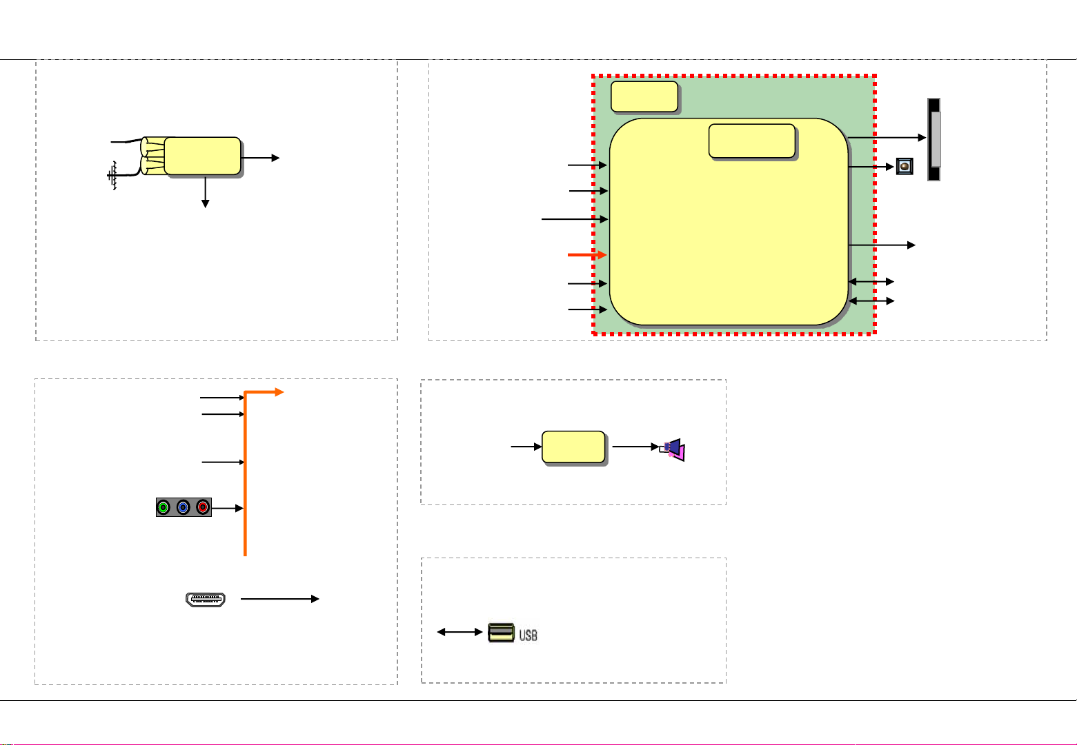
1. Power-Up Boot Fail Trouble Shooting
(Front-end)
Cable
(External Input)
ISDB-T/
PAL/NTSC
IF
AV1
AV1_LR
COMP1_LR
CVBS_LIVE
SIF1
(System + Scalar)
(Audio Out)
I2S_S7LR
CVBS_LIVE
TP1
SIF_LIVE
EXT_IN
HDMI_D
HDMI_C
TAS5733
Serial_Flash
1MB
DDR2
64MB(32*2)
Main IC
(Micom)
Main IC inner PM
LVDS
SPDIF
USB2.0
FHD
I2S_S7LR
Rear(0)
Side(1)
SIDE HDMI_PORT
HDMI_Rear(D port)
Only for training and service purposes
EXT_IN
(Comp1)
(USB)
Side USB
LGE Internal Use Only Copyright © 2013 LG Electronics Inc. All rights reserved.
Page 22
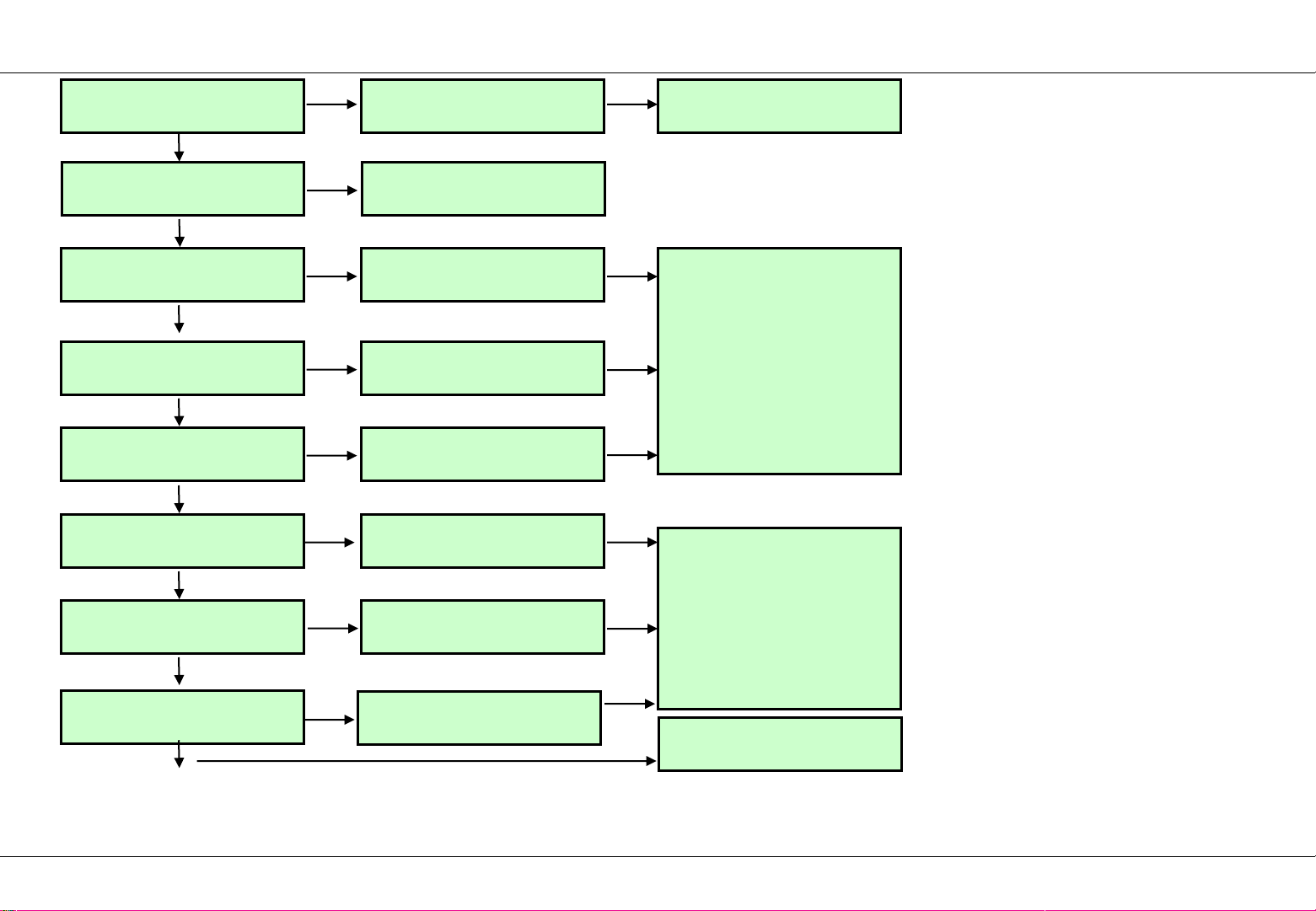
1. Power-Up Boot Fail Trouble Shooting
Check P600 All Voltage Level
(5V_ST)
Y
Check All Voltage Level
at Bead, RL_ON, IC400 output
Y
Check Voltage Level 1.15 at IC603,
L605(+1.15V_VDDC)
Y
Check Voltage Level 1.8V
at R675(+1.8V_DDR)
Y
Check Voltage Level 3.3V at L604
(Main IC supply voltage)
Y
Check X400 Clock 24MHz
N Y
N
N
N
N
N
Check Power connector
Replace one of Bead, IC400
& Recheck
Replace of the IC603
& Recheck
Replace of the IC613
& Recheck
Replace of the IC600
& Recheck
Replace X400
N
N
N
N
Replace Power board
Check SW Redownload or replace
Y
Check signal transition
at IC505
Y
Check signal transition
IC504
Y
Only for training and service purposes
N
Maybe Serial Flash Memory problem
N
Maybe NAND Flash Memory or
IC400 have troubles
Check Main chip and Soc_Reset
N
N
Signal from PM GPIO
DC
AC
Check DDR Memory
/Replace one
LGE Internal Use Only Copyright © 2013 LG Electronics Inc. All rights reserved.
Page 23
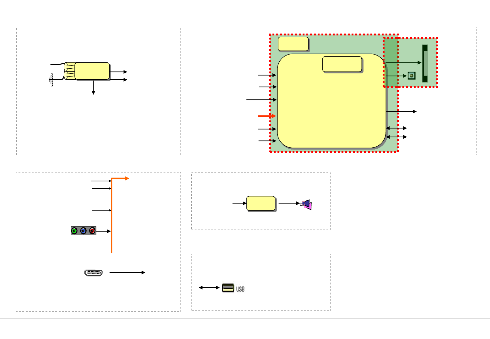
2. No OSD Trouble Shooting
(Front-end)
Cable
(External Input)
ISDB-T/
PAL/NTSC
IF
AV1
AV1_LR
COMP1_LR
CVBS_LIVE
SIF1
TP1
(System + Scalar)
(Audio Out)
I2S_S7R
CVBS_LIVE
TP1
SIF_LIVE
EXT_IN
HDMI_D
HDMI_C
TAS5733
Serial_Flash
1MB
DDR2
64MB(32*2)
Main IC
LVDS
SPDIF
USB2.0
FHD
I2S_S7LR
Rear(0)
Side(1)
SIDE HDMI_PORT
HDMI_Rear(D port)
Only for training and service purposes
EXT_IN
(Comp1/)
(USB)
Side USB
LGE Internal Use Only Copyright © 2013 LG Electronics Inc. All rights reserved.
Page 24
2. No OSD Trouble Shooting
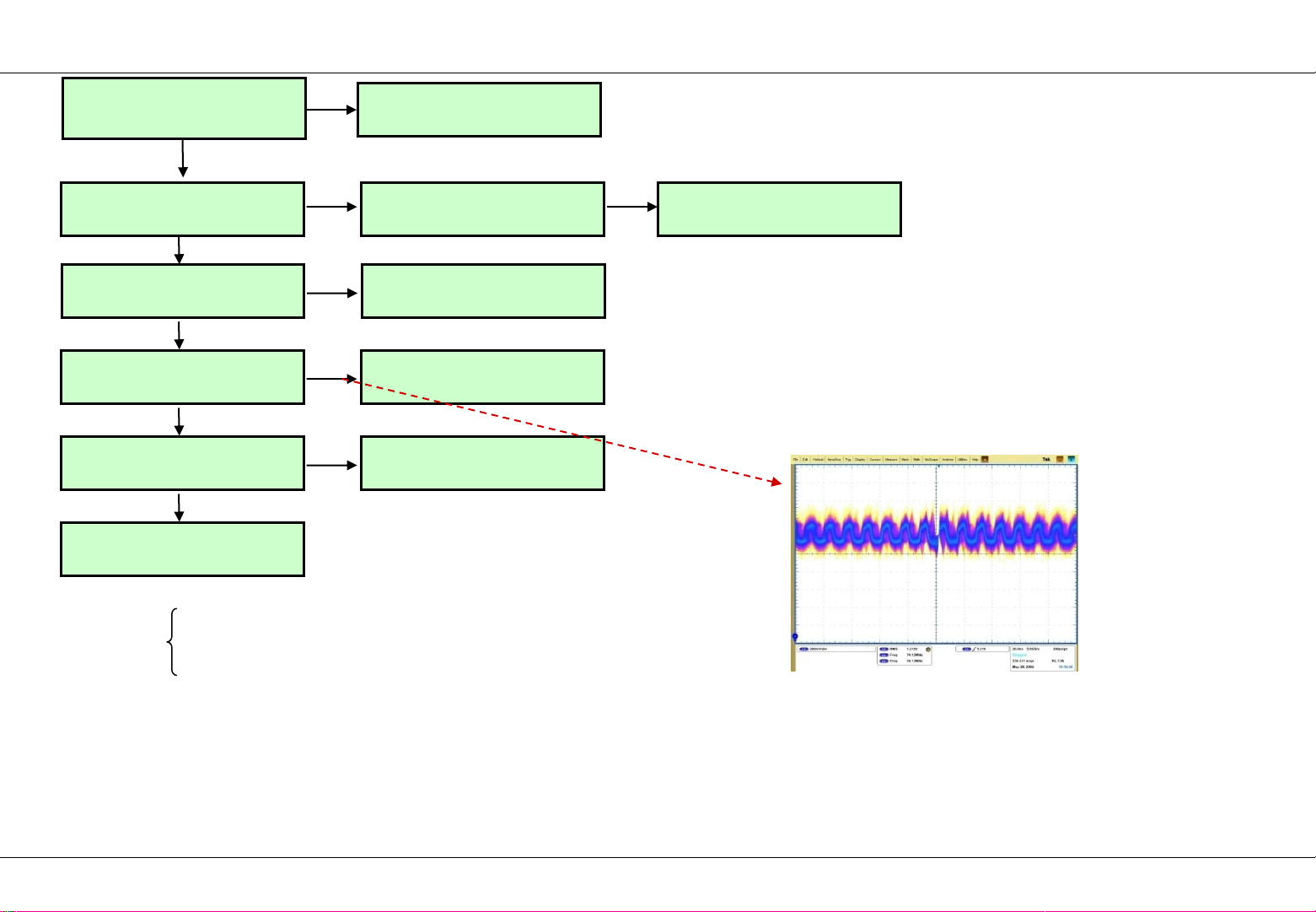
Check P600
5V_ON
Y
Check 5V Voltage Level
at P600
Y
Check 5V Voltage Level
at L600
Y
Check P500/P503
(RXAC-), (RXAC+), (RXBC-),
(RXBC+), Display Enable
Y
Check LVDS Cable
Y
Check PDP Module
N
N Y
N
N
N
Check GPIO Path of PM
Check Power connector
Replace one of L600
& Recheck
Maybe IC400
has troubles
Replace Cable
Replace Power board
Electrical Specifications
Check CAS
Power Supply Sequence
Input Signal Timing Specification
Control Signal Register
Only for training and service purposes
It should satisfy the Pixel Clock on CAS.
LGE Internal Use Only Copyright © 2013 LG Electronics Inc. All rights reserved.
Page 25
2-1Module Control Trouble Shooting
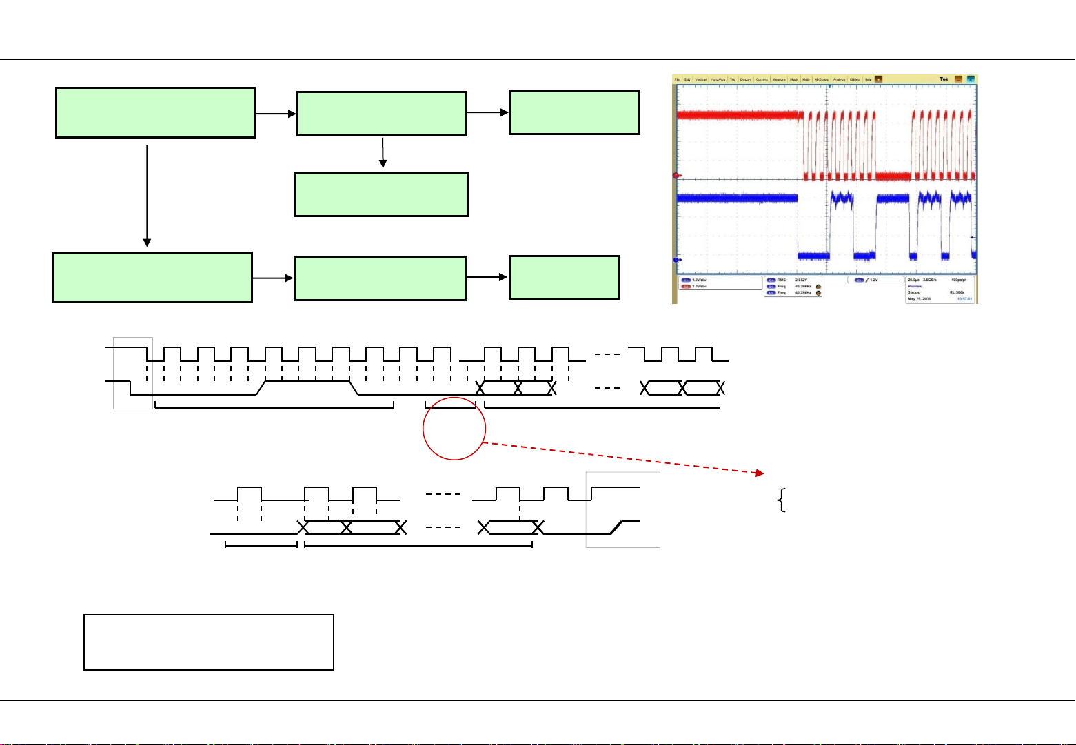
“TILT” on Adjust Remocon
: PDP internal pattern displays?
Y
PDP Module is OK.
Check SCL,SDA line
1
SCL
0 0
SDA
Start
By
0
Chip ID Address Byte
Master
SCL (continue)
SDA (continue)
N
N
1 1 1
(0x1C)
9 1
PDP Module Power is OK?
Y
Replace PDP Module
Check Signal
output
W
0
Write
only
By Slave
D7
D6
9
ACK
N
Check SMPS & cable
SCL
SDA
N
Replace Control
1
A7
A6
Board
< Sample Signal >
8
A1 A0
Command Address
Addr=A[7:0]
9
ACK signal Check
Low : OK
High : Error
D0
By Slave
Master : Image Board
Slave : PDP Module
Only for training and service purposes
ACK
Command Data
for Addr
ACK
By Slave
Stop
By Master
* Module I2C check
* 조정메뉴 Module ver. 확인
LGE Internal Use Only Copyright © 2013 LG Electronics Inc. All rights reserved.
Page 26
3. Digital TV Video Trouble Shooting
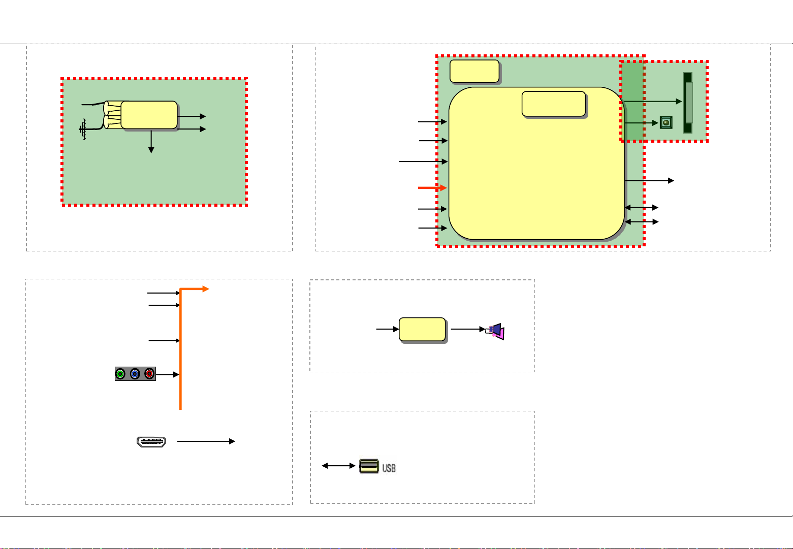
(Front-end)
Cable
(External Input)
ISDB-T/
PAL/NTSC
IF
AV1
AV1_LR
COMP1_LR
CVBS_LIVE
SIF1
TP1
(System + Scalar)
(Audio Out)
I2S_S7R
CVBS_LIVE
TP1
SIF_LIVE
EXT_IN
HDMI_D
HDMI_C
TAS5733
Serial_Flash
1MB
DDR2
64MB(32*2)
Main IC
LVDS
SPDIF
USB2.0
FHD
I2S_S7LR
Rear(0)
Side(1)
SIDE HDMI_PORT
HDMI_Rear(D port)
Only for training and service purposes
EXT_IN
(Comp1)
(USB)
Side USB
LGE Internal Use Only Copyright © 2013 LG Electronics Inc. All rights reserved.
Page 27
3. Digital TV Video Trouble Shooting
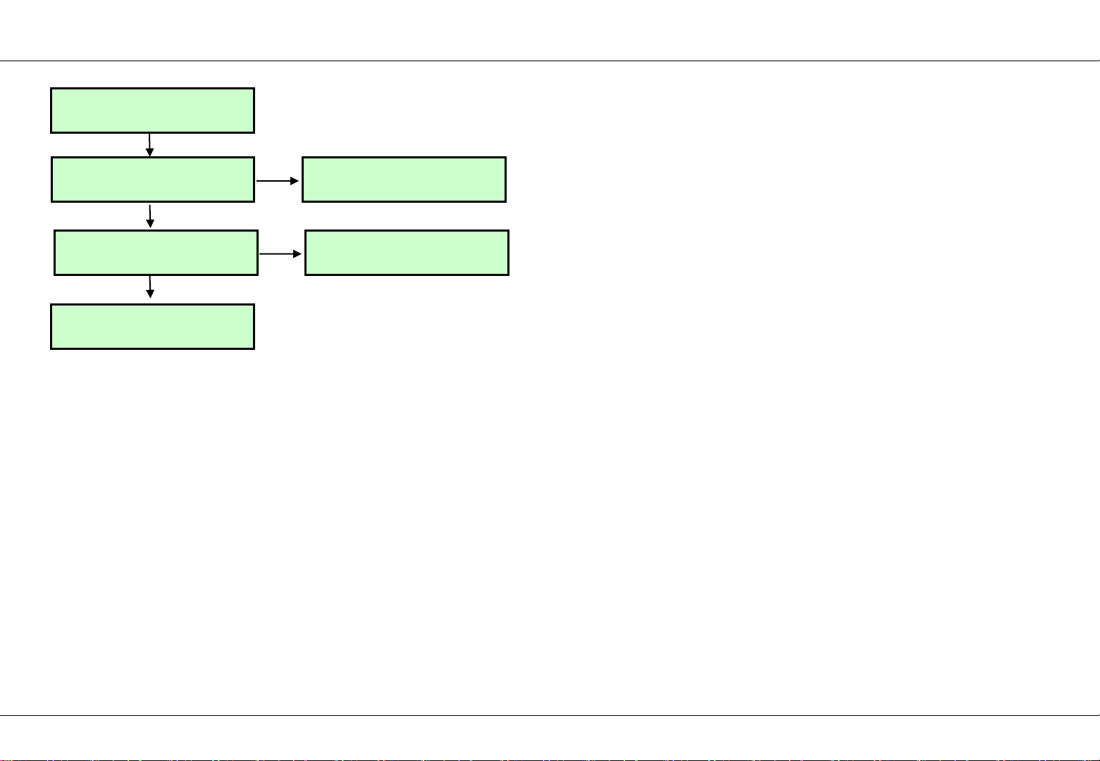
Check RF Cable
Y
Check Tuner Power
(3.3V, 1.1V)
Y
Check IF Signal pin
Y
Maybe Mstar IC400
has problems
N
Replace one of Bead
& Recheck
* Tuner I2C check
* ChangeTuner type at adjust menu
N
Maybe Tuner has problems
Only for training and service purposes
LGE Internal Use Only Copyright © 2013 LG Electronics Inc. All rights reserved.
Page 28
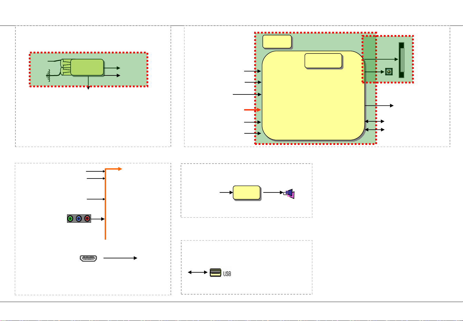
4. Analog TV Video Trouble Shooting
(Front-end)
Cable
(External Input)
ISDB-T/
PAL/NTSC
IF
AV1
AV1_LR
COMP1_LR
CVBS_LIVE
SIF1
TP1
(System + Scalar)
(Audio Out)
I2S_S7R
CVBS_LIVE
TP1
SIF_LIVE
EXT_IN
HDMI_D
HDMI_C
TAS5733
Serial_Flash
1MB
DDR2
64MB(32*2)
Main IC
LVDS
SPDIF
USB2.0
FHD
I2S_S7LR
Rear(0)
Side(1)
SIDE HDMI_PORT
HDMI_Rear(D port)
Only for training and service purposes
EXT_IN
(Comp1)
(USB)
Side USB
LGE Internal Use Only Copyright © 2013 LG Electronics Inc. All rights reserved.
Page 29
4. Analog TV Video Trouble Shooting
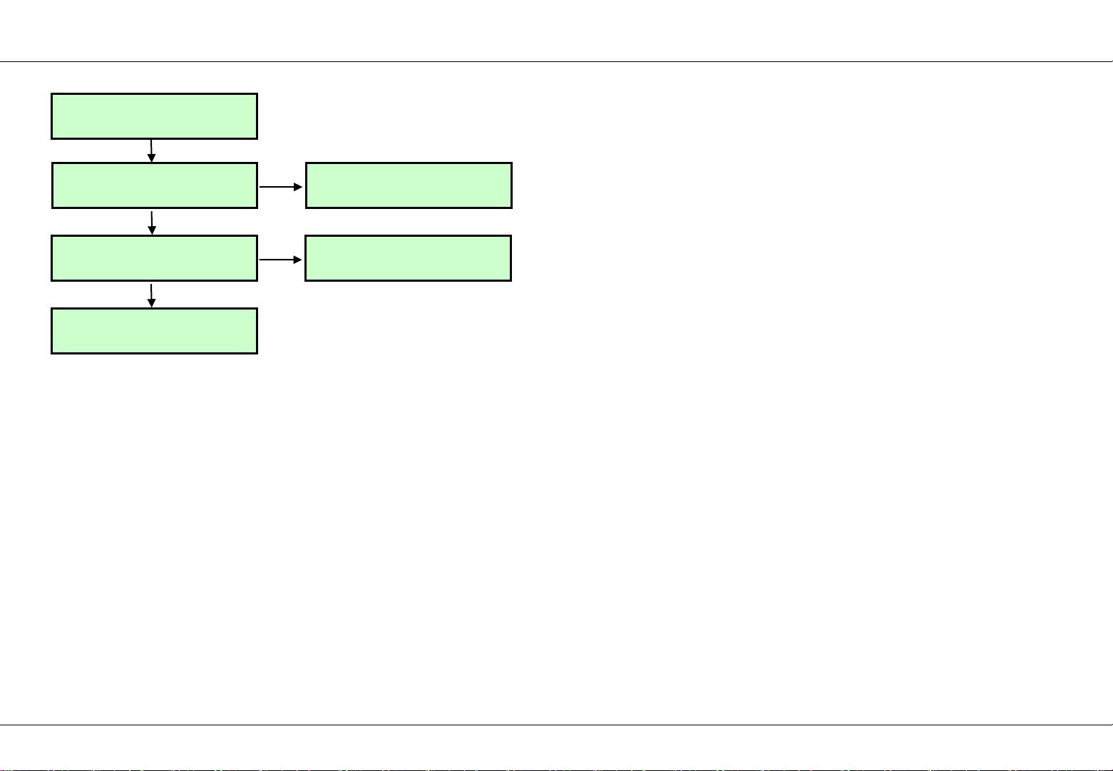
Check RF Cable
Y
Check Tuner Power
(3.3V,1.1V)
Y
Check CVBS Signal
Y
Maybe Mstar IC400
has problems
N
N
Replace one of
IC608,L606
& Recheck
Maybe Tuner has problems
Only for training and service purposes
LGE Internal Use Only Copyright © 2013 LG Electronics Inc. All rights reserved.
Page 30
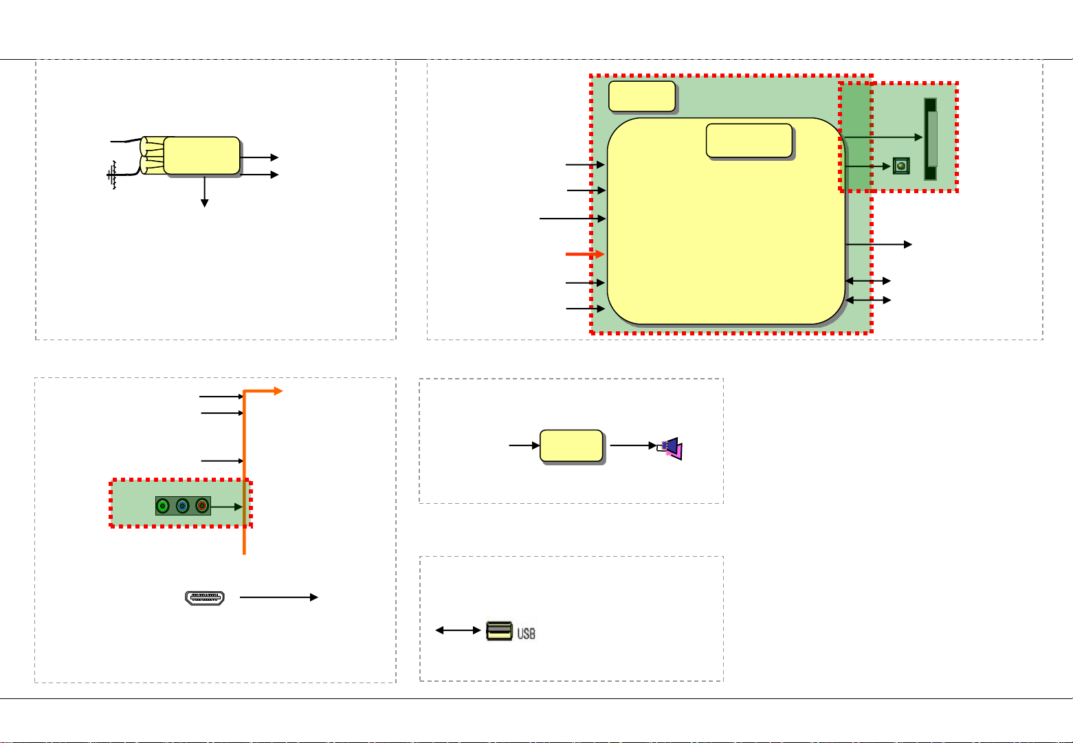
5. Component Video Trouble Shooting
(Front-end)
Cable
(External Input)
ISDB-T/
PAL/NTSC
IF
AV1
AV1_LR
COMP1_LR
CVBS_LIVE
SIF1
TP1
(System + Scalar)
(Audio Out)
I2S_S7R
CVBS_LIVE
TP1
SIF_LIVE
EXT_IN
HDMI_D
HDMI_C
TAS5733
Serial_Flash
1MB
DDR2
64MB(32*2)
Main IC
LVDS
SPDIF
USB2.0
FHD
I2S_S7LR
Rear(0)
Side(1)
SIDE HDMI_PORT
HDMI_Rear(D port)
Only for training and service purposes
EXT_IN
(Comp1/2, RGB)
(USB)
Side USB
LGE Internal Use Only Copyright © 2013 LG Electronics Inc. All rights reserved.
Page 31
5. Component &SCART Video Trouble Shooting
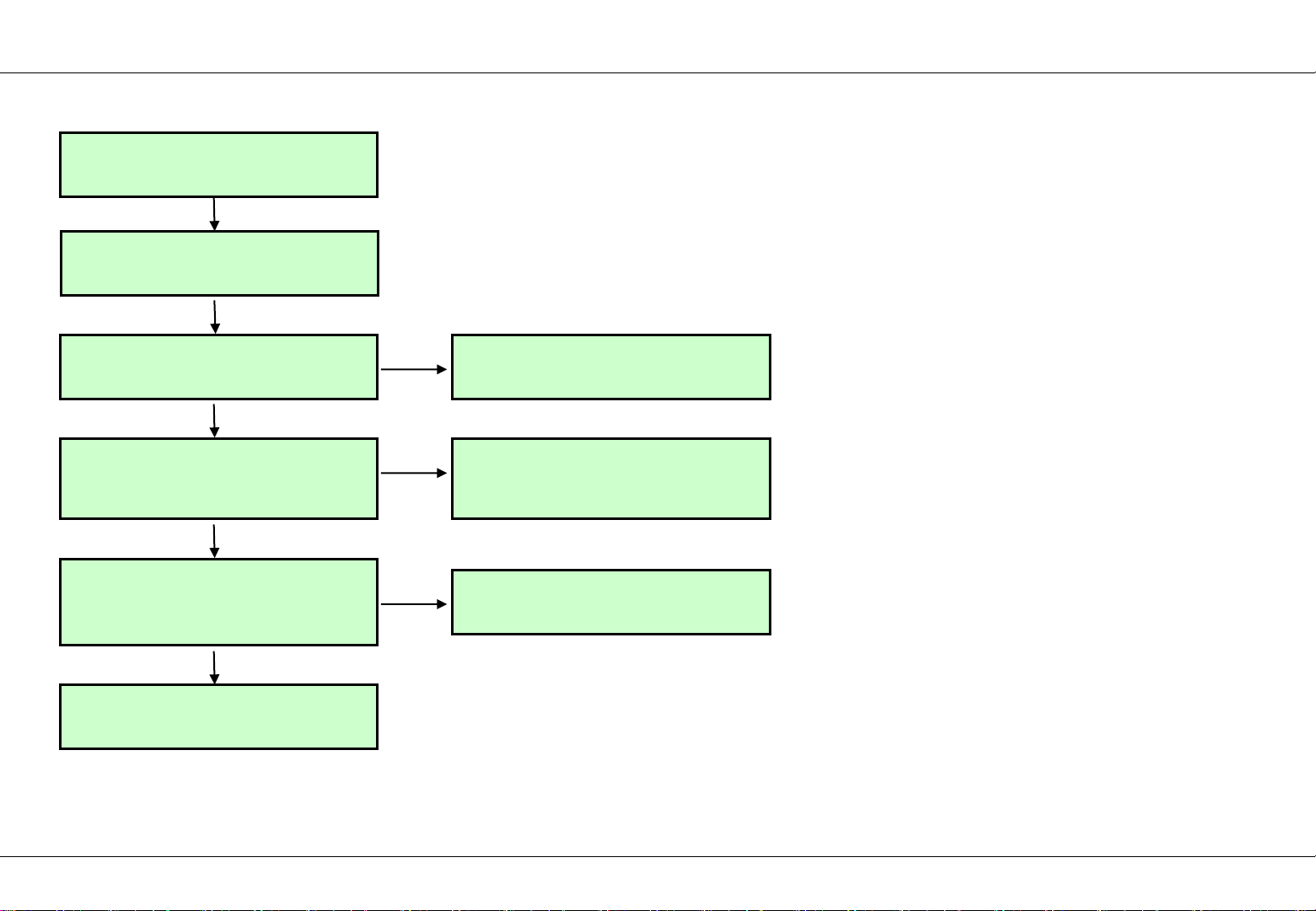
Check Signal Format
Is it supported signal?
Y
Check Component Cable
Y
Check Component Jack JK210
Y
Check Component Signal
R251/R252/R253
R106/R107/R108
(Termination resistor)
Y
Check Component Signal
R429/R436/R438
R446/R444/R434
Main IC Input
Y
Maybe Mstar IC400
has problems
N
N
N
Replace Jack
Replace one of
R251/R252/R253
R106/R107/R108
& Recheck
Replace it
Only for training and service purposes
LGE Internal Use Only Copyright © 2013 LG Electronics Inc. All rights reserved.
Page 32
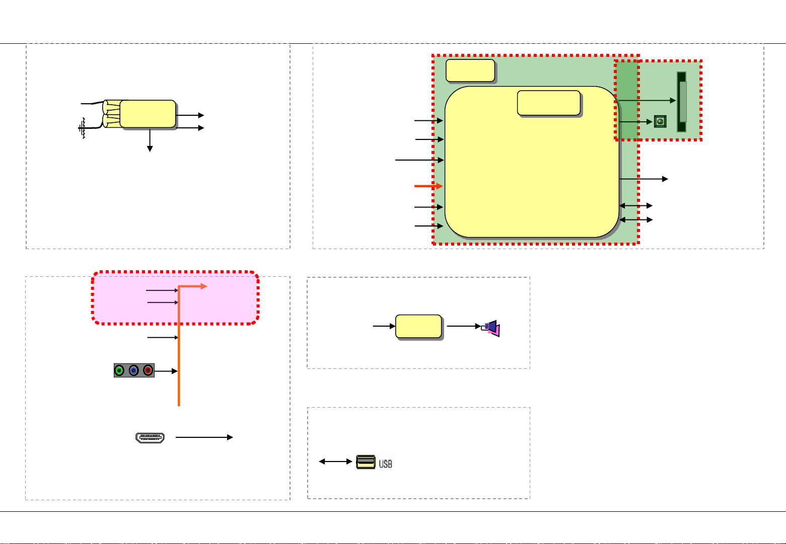
6. AV Video Trouble Shooting
(Front-end)
Cable
(External Input)
ISDB-T/
PAL/NTSC
IF
AV1
AV1_LR
COMP1_LR
CVBS_LIVE
SIF1
TP1
(System + Scalar)
(Audio Out)
I2S_S7R
CVBS_LIVE
TP1
SIF_LIVE
EXT_IN
HDMI_D
HDMI_C
TAS5733
Serial_Flash
1MB
DDR2
64MB(32*2)
Main IC
LVDS
SPDIF
USB2.0
FHD
I2S_S7LR
Rear(0)
Side(1)
SIDE HDMI_PORT
HDMI_Rear(D port)
Only for training and service purposes
EXT_IN
(Comp1)
(USB)
Side USB
LGE Internal Use Only Copyright © 2013 LG Electronics Inc. All rights reserved.
Page 33
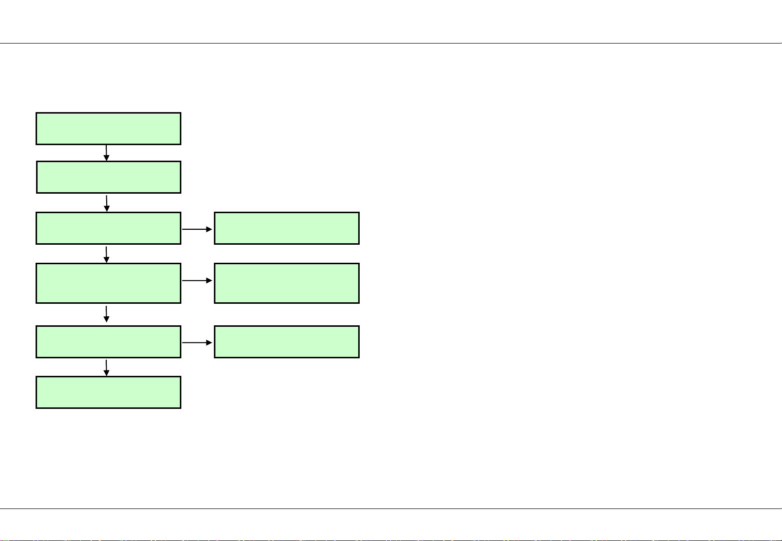
7. AV Video Trouble Shooting
Check Signal Format
Is it supported signal?
Y
Check AV Cable
Y
Check Jack JK211/JK208
Y
Check CVBS Signal
R424/426
N
N
Replace Jack
Replace one of
R424/426
& Recheck
Y
Check CVBS Signal
R4425
Y
Maybe Mstar IC400
has problems
Only for training and service purposes
N
Replace one of
R4285& Recheck
LGE Internal Use Only Copyright © 2013 LG Electronics Inc. All rights reserved.
Page 34
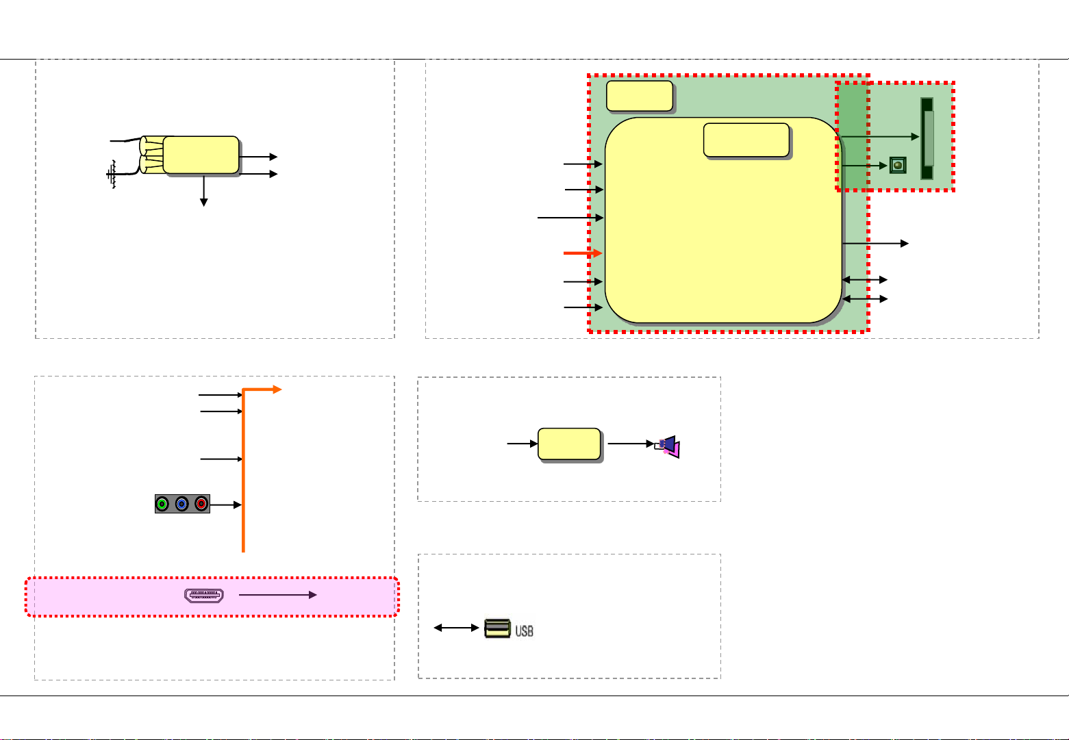
8. HDMI Video Trouble Shooting
(Front-end)
Cable
(External Input)
ISDB-T/
PAL/NTSC
IF
AV1
AV1_LR
COMP1_LR
CVBS_LIVE
SIF1
TP1
(System + Scalar)
(Audio Out)
I2S_S7R
CVBS_LIVE
TP1
SIF_LIVE
EXT_IN
HDMI_D
HDMI_C
TAS5733
Serial_Flash
1MB
DDR2
64MB(32*2)
Main IC
LVDS
SPDIF
USB2.0
FHD
I2S_S7LR
Rear(0)
Side(1)
SIDE HDMI_PORT
HDMI_Rear(D port)
Only for training and service purposes
EXT_IN
(Comp1)
(USB)
Side USB
LGE Internal Use Only Copyright © 2013 LG Electronics Inc. All rights reserved.
Page 35
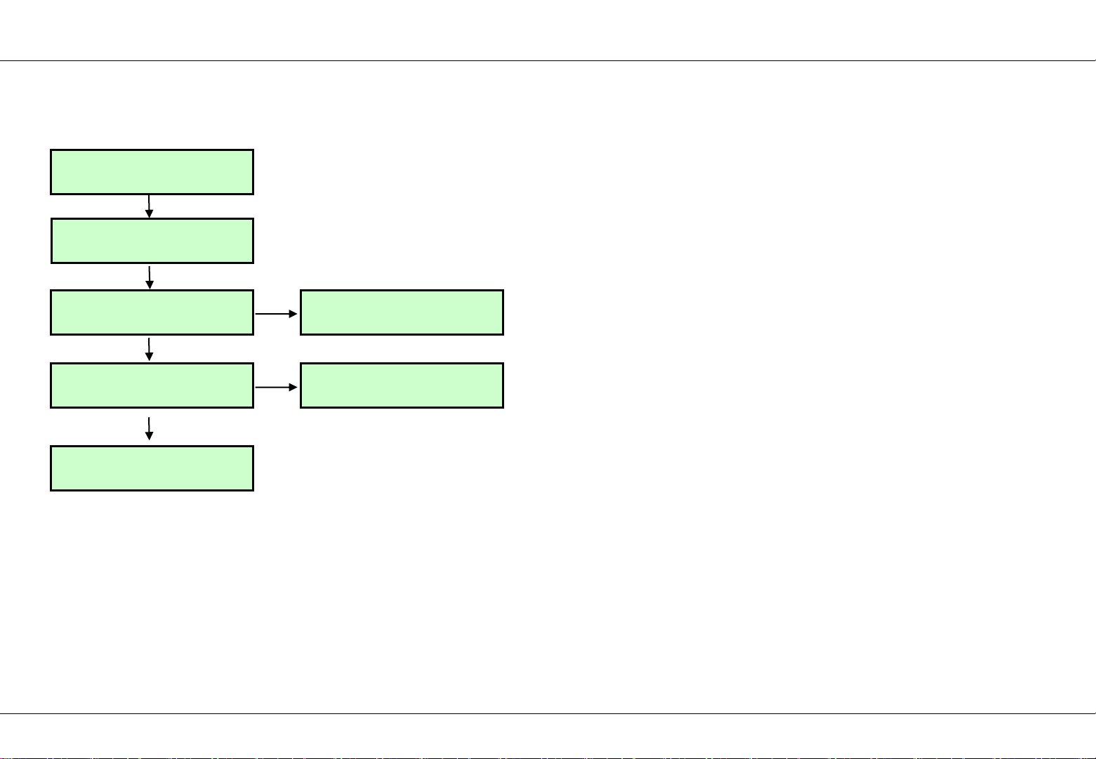
8. HDMI Video Trouble Shooting
Check Signal Format
Is it supported signal?
Y
Check HDMI Cable
Y
Check HDMI Jack
JK200,JK201
Y
N
Replace Jack
Check I2C Signal(EEPROM)
R231/R2246, R207/R2208
Y
Maybe Mstar IC400
has problems
Only for training and service purposes
N
Replace It & Recheck
LGE Internal Use Only Copyright © 2013 LG Electronics Inc. All rights reserved.
Page 36
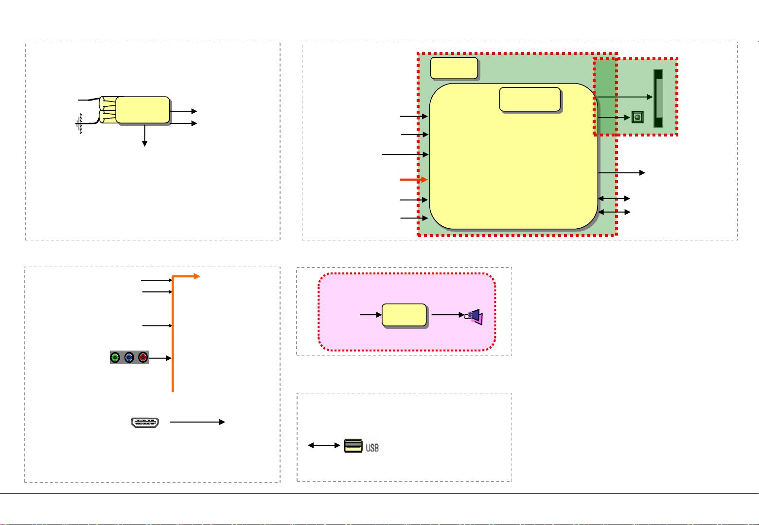
9. All Source Audio Trouble Shooting
(Front-end)
Cable
(External Input)
ISDB-T/
PAL/NTSC
IF
AV1
AV1_LR
COMP1_LR
CVBS_LIVE
SIF1
TP1
(System + Scalar)
(Audio Out)
I2S_S7R
CVBS_LIVE
TP1
SIF_LIVE
EXT_IN
HDMI_D
HDMI_C
TAS5733
Serial_Flash
1MB
DDR2
64MB(32*2)
Main IC
LVDS
SPDIF
USB2.0
FHD
I2S_S7LR
Rear(0)
Side(1)
SIDE HDMI_PORT
HDMI_Rear(D port)
Only for training and service purposes
EXT_IN
(Comp1)
(USB)
Side USB
LGE Internal Use Only Copyright © 2013 LG Electronics Inc. All rights reserved.
Page 37
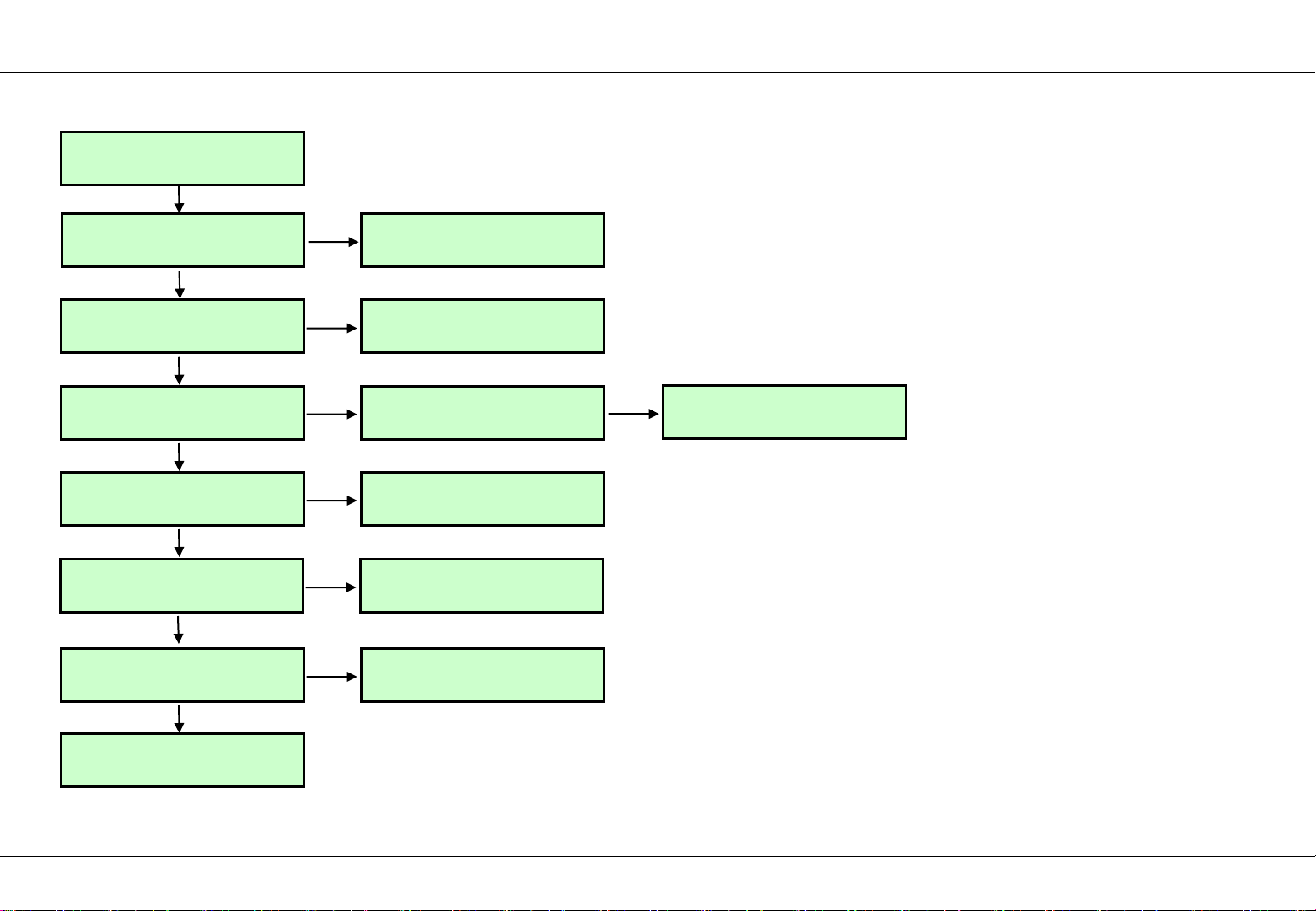
9. All Source Audio Trouble Shooting
Make sure you can’t hear any audio
Y
Check Speaker
Y
Check Connector 601
Y
Check Signal
L609,L602,L603,L610
Y
Check IC606 Power
17V, 3.3V
Y
Check Reset signal
R628
Y
Check Mstar S7R I2S Output
AR600
N
N
N
N
N
Replace Speaker
Replace Connector
Replace one of
Capacitor, Register
& Recheck
Replace It & Recheck
Replace It & Recheck (IC101)
N
Maybe STA380 has problems.
Replace It
* Amp. I2C check
N
Replace It & Recheck
Y
Maybe Mstar IC400
has problems
Only for training and service purposes
LGE Internal Use Only Copyright © 2013 LG Electronics Inc. All rights reserved.
Page 38
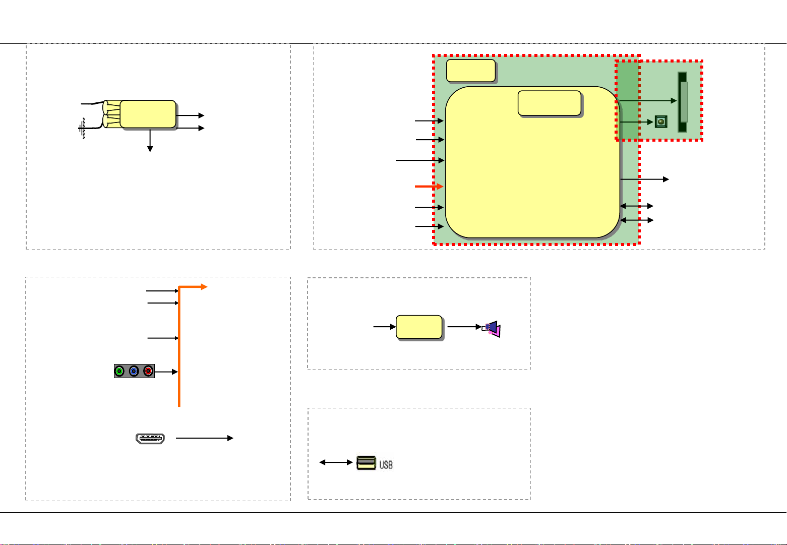
10. Digital TV Audio Trouble Shooting
(Front-end)
Cable
(External Input)
ISDB-T/
PAL/NTSC
IF
AV1
AV1_LR
COMP1_LR
CVBS_LIVE
SIF1
TP1
(System + Scalar)
(Audio Out)
I2S_S7R
CVBS_LIVE
TP1
SIF_LIVE
EXT_IN
HDMI_D
HDMI_C
TAS5733
Serial_Flash
1MB
DDR2
64MB(32*2)
Main IC
LVDS
SPDIF
USB2.0
FHD
I2S_S7LR
Rear(0)
Side(1)
SIDE HDMI_PORT
HDMI_Rear(D port)
Only for training and service purposes
EXT_IN
(Comp1/
(USB)
Side USB
LGE Internal Use Only Copyright © 2013 LG Electronics Inc. All rights reserved.
Page 39
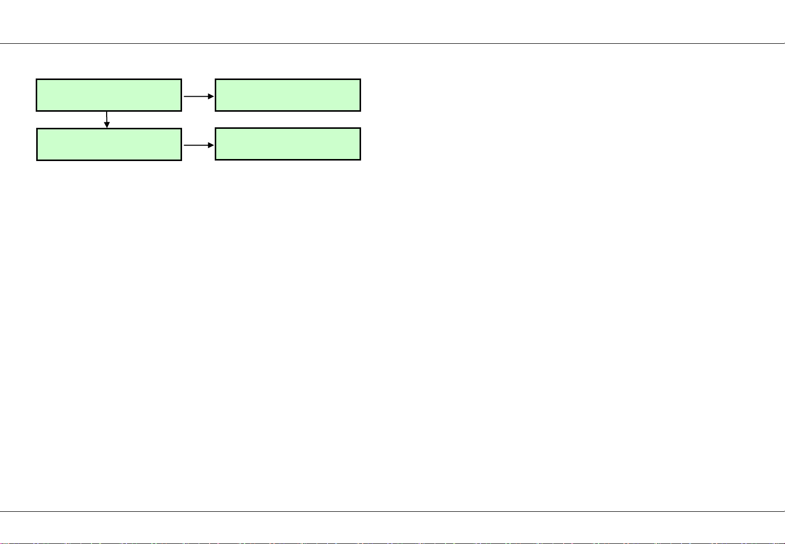
10. Digital TV Audio Trouble Shooting
Check video output
Y
Follow procedure All source audio
trouble shooting
N
N
Follow procedure digital TV video
trouble shooting
Maybe Mster internal audio DSP has
problems.
Replace It
Only for training and service purposes
LGE Internal Use Only Copyright © 2013 LG Electronics Inc. All rights reserved.
Page 40
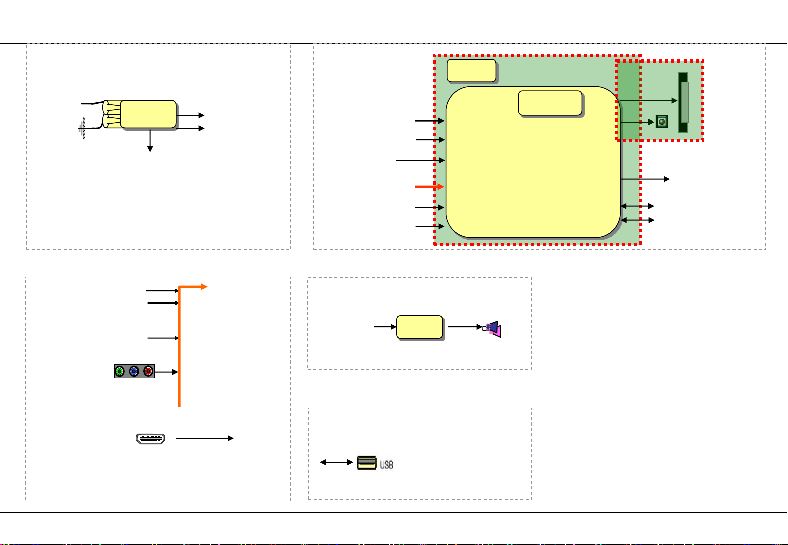
11. Analog TV Audio Trouble Shooting
(Front-end)
Cable
(External Input)
ISDB-T/
PAL/NTSC
IF
AV1
AV1_LR
COMP1_LR
CVBS_LIVE
SIF1
TP1
(System + Scalar)
(Audio Out)
I2S_S7R
CVBS_LIVE
TP1
SIF_LIVE
EXT_IN
HDMI_D
HDMI_C
TAS5733
Serial_Flash
1MB
DDR2
64MB(32*2)
Main IC
LVDS
SPDIF
USB2.0
FHD
I2S_S7LR
Rear(0)
Side(1)
SIDE HDMI_PORT
HDMI_Rear(D port)
Only for training and service purposes
EXT_IN
(Comp1)
(USB)
Side USB
LGE Internal Use Only Copyright © 2013 LG Electronics Inc. All rights reserved.
Page 41
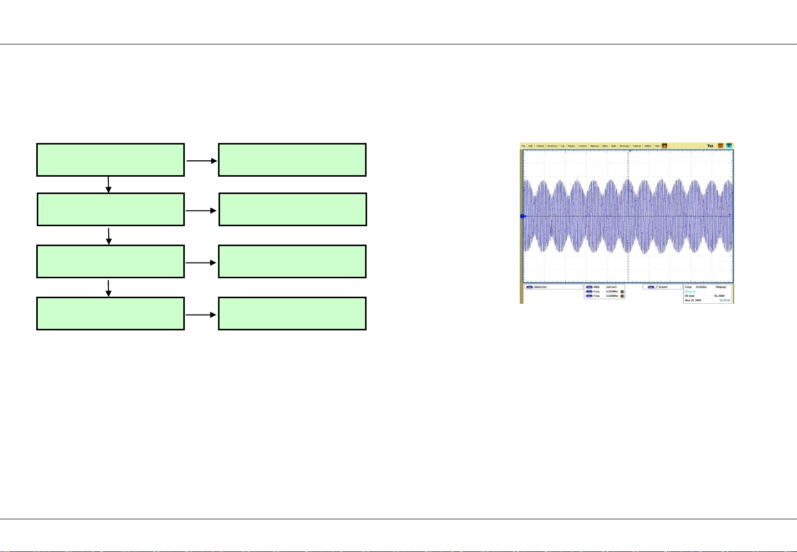
11. Analog TV Audio Trouble Shooting
Check video output
Y
Check Tuner Power
Y
Check SIF Signal
Y
Follow procedure All source audio
trouble shooting
N
N
N
N
Follow procedure analog TV video
trouble shooting
Replace one of IC608,IC604,IC602
& Recheck
Maybe Tuner has problems
Maybe Mstar audio block has
problems.
Replace It
< SIF waveform – sample >
- Defend on the input signal.
Only for training and service purposes
LGE Internal Use Only Copyright © 2013 LG Electronics Inc. All rights reserved.
Page 42
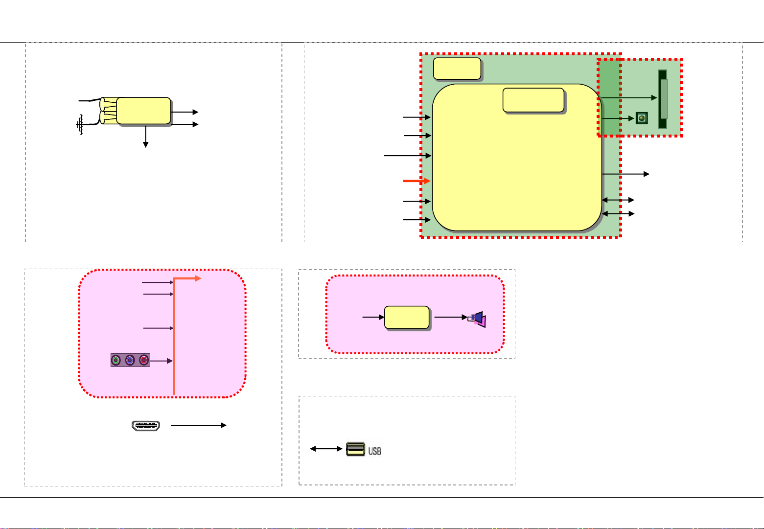
12. Component / AV Audio Trouble Shooting
(Front-end)
Cable
(External Input)
ISDB-T/
PAL/NTSC
IF
AV1
AV1_LR
COMP1_LR
CVBS_LIVE
SIF1
TP1
(System + Scalar)
(Audio Out)
I2S_S7R
CVBS_LIVE
TP1
SIF_LIVE
EXT_IN
HDMI_D
HDMI_C
TAS5733
Serial_Flash
1MB
DDR2
64MB(32*2)
Main IC
LVDS
SPDIF
USB2.0
FHD
I2S_S7LR
Rear(0)
Side(1)
SIDE HDMI_PORT
HDMI_Rear(D port)
Only for training and service purposes
EXT_IN
(Comp1)
(USB)
Side USB
LGE Internal Use Only Copyright © 2013 LG Electronics Inc. All rights reserved.
Page 43
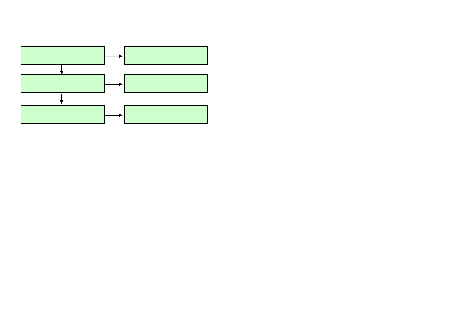
12. Component / RGB / AV Audio Trouble Shooting
Check Video Output
Y
Check Jack JK211,JK202,JK205
Y
Follow procedure All source audio
trouble shooting
N
N
N
Follow procedure external input
video trouble shooting
Replace Jack
Maybe Mstar audio block has
problems.
Replace It
Only for training and service purposes
LGE Internal Use Only Copyright © 2013 LG Electronics Inc. All rights reserved.
Page 44
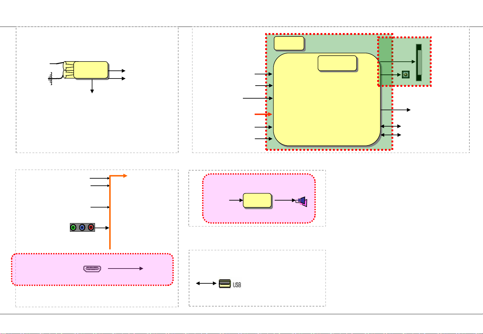
13. HDMI Audio Trouble Shooting
(Front-end)
Cable
(External Input)
ISDB-T/
PAL/NTSC
IF
AV1
AV1_LR
COMP1_LR
CVBS_LIVE
SIF1
TP1
(System + Scalar)
(Audio Out)
I2S_S7R
CVBS_LIVE
TP1
SIF_LIVE
EXT_IN
HDMI_D
HDMI_C
TAS5733
Serial_Flash
1MB
DDR2
64MB(32*2)
Main IC
LVDS
SPDIF
USB2.0
FHD
I2S_S7LR
Rear(0)
Side(1)
SIDE HDMI_PORT
HDMI_Rear(D port)
Only for training and service purposes
EXT_IN
(Comp1)
(USB)
Side USB
LGE Internal Use Only Copyright © 2013 LG Electronics Inc. All rights reserved.
Page 45
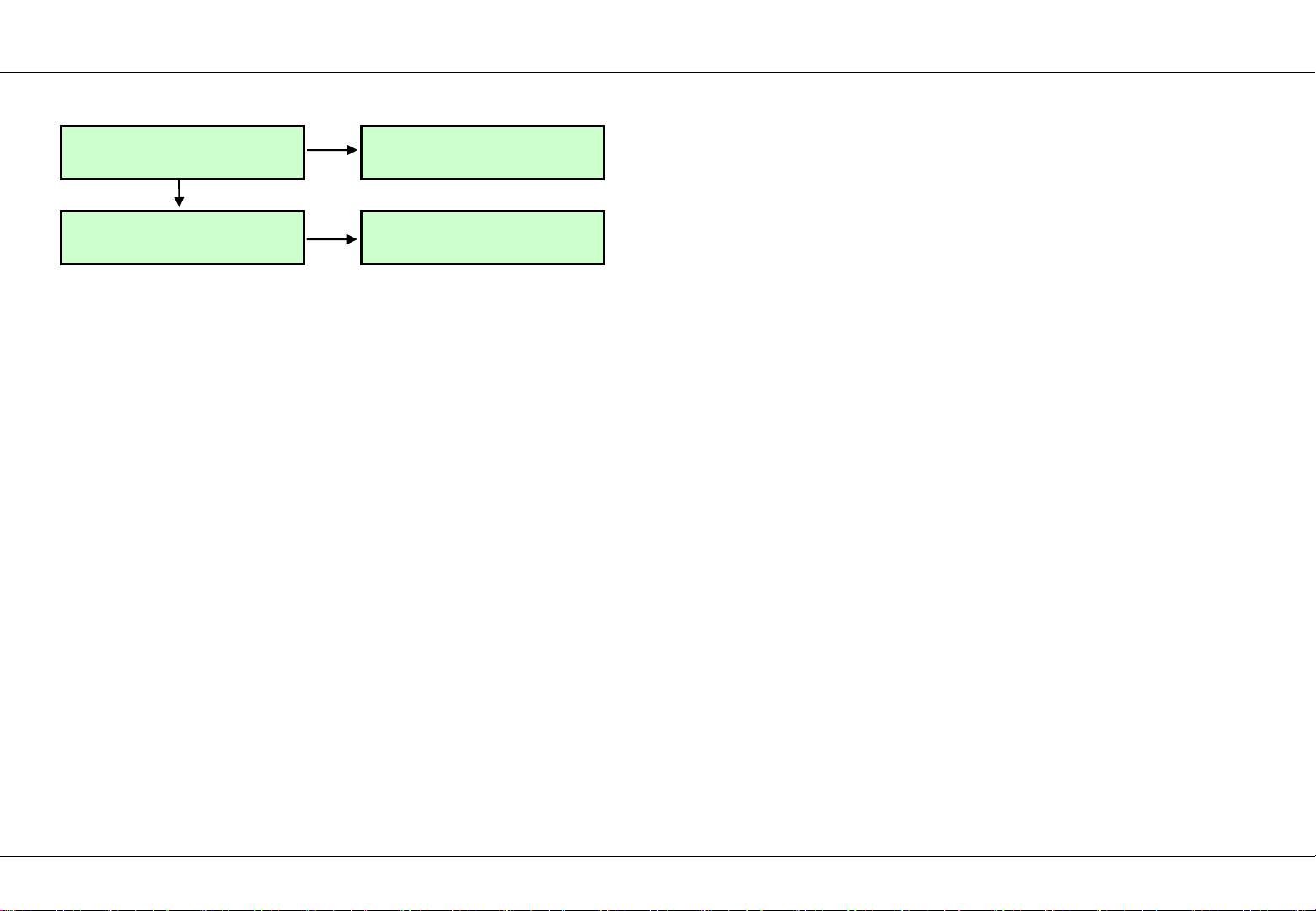
13. HDMI Audio Trouble Shooting
Check video output
Y
Follow procedure All source audio
trouble shooting
N
N
Follow procedure HDMI video
trouble shooting
Maybe Mstar audio block has
problems.
Replace it
Only for training and service purposes
LGE Internal Use Only Copyright © 2013 LG Electronics Inc. All rights reserved.
Page 46
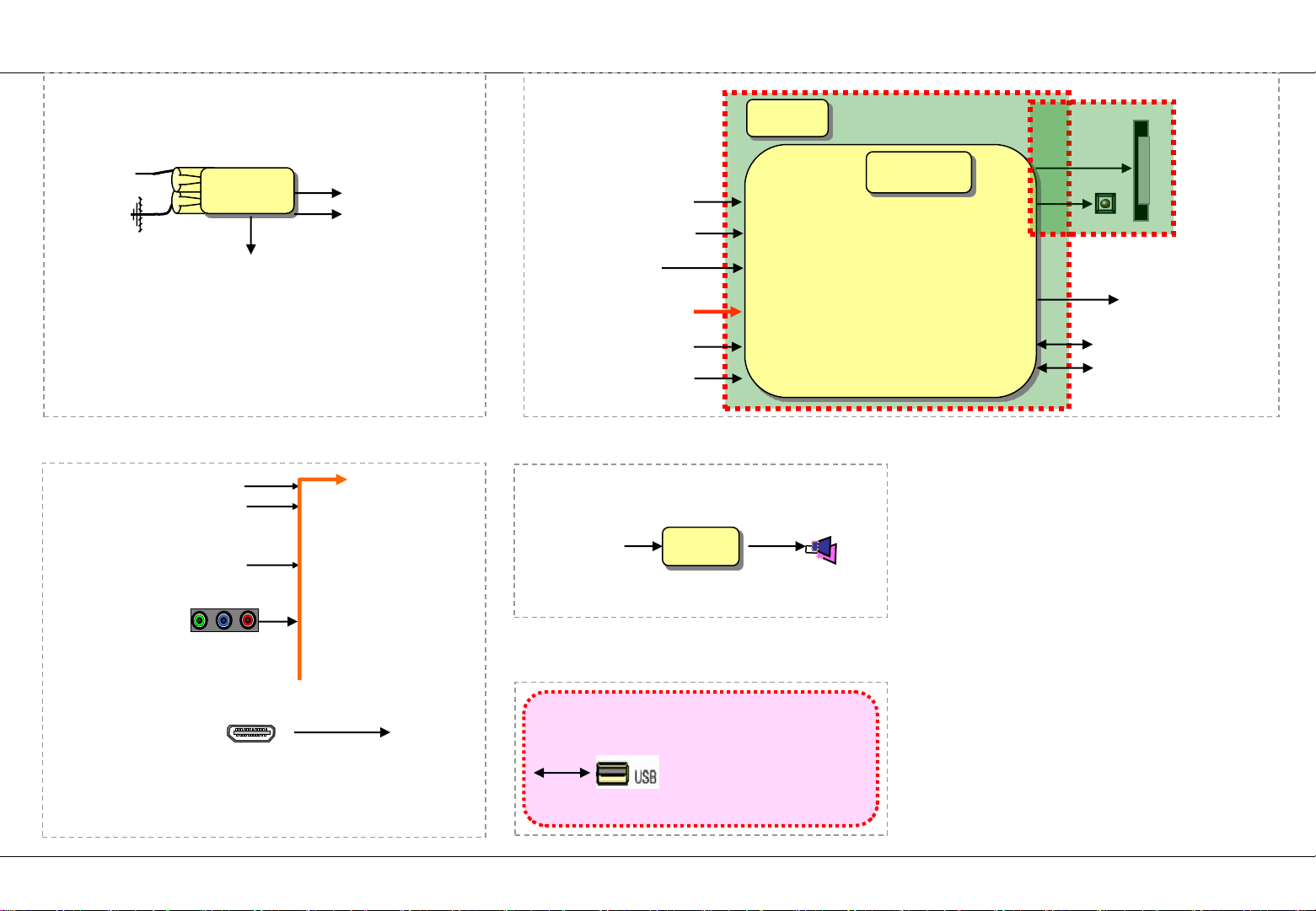
14. USB Trouble Shooting
(Front-end)
Cable
(External Input)
ISDB-T/
PAL/NTSC
IF
AV1
AV1_LR
COMP1_LR
CVBS_LIVE
SIF1
TP1
(System + Scalar)
(Audio Out)
I2S_S7R
CVBS_LIVE
TP1
SIF_LIVE
EXT_IN
HDMI_D
HDMI_C
TAS5733
Serial_Flash
1MB
DDR2
64MB(32*2)
Main IC
LVDS
SPDIF
USB2.0
FHD
I2S_S7LR
Rear(0)
Side(1)
SIDE HDMI_PORT
HDMI_Rear(D port)
Only for training and service purposes
EXT_IN
(Comp1)
(USB)
Side USB
LGE Internal Use Only Copyright © 2013 LG Electronics Inc. All rights reserved.
Page 47
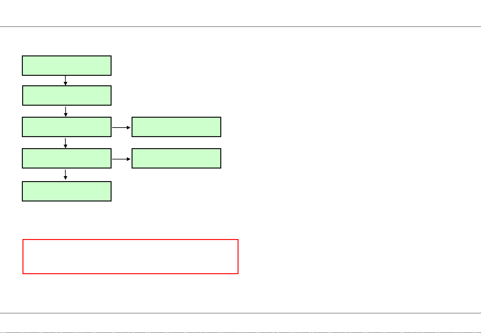
14. USB Trouble Shooting
Check USB 2.0 Cable
Y
Check USB device
If device is 2.5 inch HDD,
Check power adaptor
Y
Check JK209
Y
Check 5V voltage level
Y
Maybe Mstar IC400
has problems. Replace It.
N
N
Replace IC204 & Recheck
Replace Jack
• Exception
- USB power could be disabled by inrushing current
- In this case, remove the device and try to reboot the TV (AC power off/on)
Only for training and service purposes
LGE Internal Use Only Copyright © 2013 LG Electronics Inc. All rights reserved.
 Loading...