

Page 1
CONFIDENTIAL
LED TV
SERVICE MANUAL
CHASSIS : UA71P
MODEL : 49UJ6300 49UJ6300-UA
MODEL : 49UJ6350 49UJ6350-UC
CAUTION
BEFORE SERVICING THE CHASSIS, READ THE SAFETY PRECAUTIONS IN THIS MANUAL.
P/NO : MFL69823929 (1702-REV00)
Any reproduction, duplication, distribution (including by way of email, facsimile or other electronic means),
publication, modification, copying or transmission of this Service Manual is STRICTLY PROHIBITED unless you
have obtained the prior written consent of the LG Electronics entity from which you received this Service Manual.
The material covered by this prohibition includes, without limitation, any text, graphics or logos in this Service
Manual.
Copyright © 2017 LG Electronics Inc. All rights reserved.
Only training and service purposes
Page 2

CONTENTS
CONTENTS .............................................................................................. 2
SAFETY PRECAUTIONS ........................................................................ 3
SERVICING PRECAUTIONS ................................................................... 4
SPECIFICATION ....................................................................................... 6
SOFTWARE UPDATE ............................................................................. 9
BLOCK DIAGRAM ................................................................................. 10
EXPLODED VIEW .................................................................................. 20
DISASSEMBLY ....................................................................................... 21
TROUBLE SHOOTING GUIDE ................................................ APPENDIX
- 2 -
Page 3
SAFETY PRECAUTIONS
IMPORTANT SAFETY NOTICE
Many electrical and mechanical parts in this chassis have special safety-related characteristics. These parts are identified by in the
Exploded View.
It is essential that these special safety parts should be replaced with the same components as recommended in this manual to prevent
Shock, Fire, or other Hazards.
Do not modify the original design without permission of manufacturer.
General Guidance
An isolation Transformer should always be used during the
servicing of a receiver whose chassis is not isolated from the AC
power line. Use a transformer of adequate power rating as this
protects the technician from accidents resulting in personal injury
from electrical shocks.
It will also protect the receiver and it's components from being
damaged by accidental shorts of the circuitry that may be
inadvertently introduced during the service operation.
If any fuse (or Fusible Resistor) in this TV receiver is blown,
replace it with the specified.
When replacing a high wattage resistor (Oxide Metal Film Resistor,
over 1 W), keep the resistor 10 mm away from PCB.
Keep wires away from high voltage or high temperature parts.
Before returning the receiver to the customer,
always perform an AC leakage current check on the exposed
metallic parts of the cabinet, such as antennas, terminals, etc., to
be sure the set is safe to operate without damage of electrical
shock.
Leakage Current Cold Check(Antenna Cold Check)
With the instrument AC plug removed from AC source, connect an
electrical jumper across the two AC plug prongs. Place the AC
switch in the on position, connect one lead of ohm-meter to the AC
plug prongs tied together and touch other ohm-meter lead in turn to
each exposed metallic parts such as antenna terminals, phone
jacks, etc.
If the exposed metallic part has a return path to the chassis, the
measured resistance should be between 1 MΩ and 5.2 MΩ.
When the exposed metal has no return path to the chassis the
reading must be infinite.
An other abnormality exists that must be corrected before the
receiver is returned to the customer.
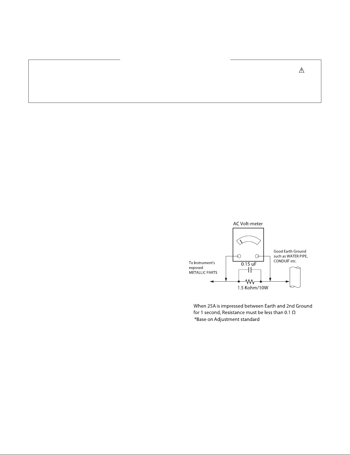
Leakage Current Hot Check (See below Figure)
Plug the AC cord directly into the AC outlet.
Do not use a line Isolation Transformer during this check.
Connect 1.5 K / 10 watt resistor in parallel with a 0.15 uF capacitor
between a known good earth ground (Water Pipe, Conduit, etc.)
and the exposed metallic parts.
Measure the AC voltage across the resistor using AC voltmeter
with 1000 ohms/volt or more sensitivity.
Reverse plug the AC cord into the AC outlet and repeat AC voltage
measurements for each exposed metallic part. Any voltage
measured must not exceed 0.75 volt RMS which is corresponds to
0.5 mA.
In case any measurement is out of the limits specified, there is
possibility of shock hazard and the set must be checked and
repaired before it is returned to the customer.
Leakage Current Hot Check circuit
- 3 -
Page 4

SERVICING PRECAUTIONS
CAUTION: Before servicing receivers covered by this service
manual and its supplements and addenda, read and follow the
SAFETY PRECAUTIONS on page 3 of this publication.
NOTE: If unforeseen circumstances create conict between the
following servicing precautions and any of the safety precautions
on page 3 of this publication, always follow the safety precautions.
Remember: Safety First.
General Servicing Precautions
1. Always unplug the receiver AC power cord from the AC power
source before;
a. Removing or reinstalling any component, circuit board mod-
ule or any other receiver assembly.
b. Disconnecting or reconnecting any receiver electrical plug or
other electrical connection.
c. Connecting a test substitute in parallel with an electrolytic
capacitor in the receiver.
CAUTION: A wrong part substitution or incorrect polarity
installation of electrolytic capacitors may result in an explosion hazard.
2. Test high voltage only by measuring it with an appropriate
high voltage meter or other voltage measuring device (DVM,
FETVOM, etc) equipped with a suitable high voltage probe.
Do not test high voltage by "drawing an arc".
3. Do not spray chemicals on or near this receiver or any of its
assemblies.
4. Unless specied otherwise in this service manual, clean
electrical contacts only by applying the following mixture to the
contacts with a pipe cleaner, cotton-tipped stick or comparable
non-abrasive applicator; 10 % (by volume) Acetone and 90 %
(by volume) isopropyl alcohol (90 % - 99 % strength)
CAUTION: This is a ammable mixture.
Unless specied otherwise in this service manual, lubrication of
contacts in not required.
5. Do not defeat any plug/socket B+ voltage interlocks with which
receivers covered by this service manual might be equipped.
6. Do not apply AC power to this instrument and/or any of its
electrical assemblies unless all solid-state device heat sinks are
correctly installed.
7. Always connect the test receiver ground lead to the receiver
chassis ground before connecting the test receiver positive
lead.
Always remove the test receiver ground lead last.
8. Use with this receiver only the test xtures specied in this
service manual.
CAUTION: Do not connect the test xture ground strap to any
heat sink in this receiver.
Electrostatically Sensitive (ES) Devices
Some semiconductor (solid-state) devices can be damaged easily by static electricity. Such components commonly are called
Electrostatically Sensitive (ES) Devices. Examples of typical ES
devices are integrated circuits and some eld-effect transistors
and semiconductor “chip” components. The following techniques
should be used to help reduce the incidence of component damage caused by static by static electricity.
1. Immediately before handling any semiconductor component or
semiconductor-equipped assembly, drain off any electrostatic
charge on your body by touching a known earth ground. Alternatively, obtain and wear a commercially available discharging
wrist strap device, which should be removed to prevent potential shock reasons prior to applying power to the unit under test.
2. After removing an electrical assembly equipped with ES
devices, place the assembly on a conductive surface such as
aluminum foil, to prevent electrostatic charge buildup or exposure of the assembly.
3. Use only a grounded-tip soldering iron to solder or unsolder ES
devices.
4. Use only an anti-static type solder removal device. Some solder
removal devices not classied as “anti-static” can generate
electrical charges sufcient to damage ES devices.
5. Do not use freon-propelled chemicals. These can generate
electrical charges sufcient to damage ES devices.
6. Do not remove a replacement ES device from its protective
package until immediately before you are ready to install it.
(Most replacement ES devices are packaged with leads electrically shorted together by conductive foam, aluminum foil or
comparable conductive material).
7. Immediately before removing the protective material from the
leads of a replacement ES device, touch the protective material
to the chassis or circuit assembly into which the device will be
installed.
CAUTION: Be sure no power is applied to the chassis or circuit,
and observe all other safety precautions.
8. Minimize bodily motions when handling unpackaged replacement ES devices. (Otherwise harmless motion such as the
brushing together of your clothes fabric or the lifting of your
foot from a carpeted oor can generate static electricity sufcient to damage an ES device.)
General Soldering Guidelines
1. Use a grounded-tip, low-wattage soldering iron and appropriate
tip size and shape that will maintain tip temperature within the
range or 500 °F to 600 °F.
2. Use an appropriate gauge of RMA resin-core solder composed
of 60 parts tin/40 parts lead.
3. Keep the soldering iron tip clean and well tinned.
4. Thoroughly clean the surfaces to be soldered. Use a mall wirebristle (0.5 inch, or 1.25 cm) brush with a metal handle.
Do not use freon-propelled spray-on cleaners.
5. Use the following unsoldering technique
a. Allow the soldering iron tip to reach normal temperature.
(500 °F to 600 °F)
b. Heat the component lead until the solder melts.
c. Quickly draw the melted solder with an anti-static, suction-
type solder removal device or with solder braid.
CAUTION: Work quickly to avoid overheating the circuit
board printed foil.
6. Use the following soldering technique.
a. Allow the soldering iron tip to reach a normal temperature
(500 °F to 600 °F)
b. First, hold the soldering iron tip and solder the strand against
the component lead until the solder melts.
c. Quickly move the soldering iron tip to the junction of the
component lead and the printed circuit foil, and hold it there
only until the solder ows onto and around both the component lead and the foil.
CAUTION: Work quickly to avoid overheating the circuit
board printed foil.
d. Closely inspect the solder area and remove any excess or
splashed solder with a small wire-bristle brush.
- 4 -
Page 5

IC Remove/Replacement
Some chassis circuit boards have slotted holes (oblong) through
which the IC leads are inserted and then bent at against the circuit foil. When holes are the slotted type, the following technique
should be used to remove and replace the IC. When working with
boards using the familiar round hole, use the standard technique
as outlined in paragraphs 5 and 6 above.
Removal
1. Desolder and straighten each IC lead in one operation by
gently prying up on the lead with the soldering iron tip as the
solder melts.
2. Draw away the melted solder with an anti-static suction-type
solder removal device (or with solder braid) before removing
the IC.
Replacement
1. Carefully insert the replacement IC in the circuit board.
2. Carefully bend each IC lead against the circuit foil pad and
solder it.
3. Clean the soldered areas with a small wire-bristle brush.
(It is not necessary to reapply acrylic coating to the areas).
"Small-Signal" Discrete Transistor
Removal/Replacement
1. Remove the defective transistor by clipping its leads as close
as possible to the component body.
2. Bend into a "U" shape the end of each of three leads remaining
on the circuit board.
3. Bend into a "U" shape the replacement transistor leads.
4. Connect the replacement transistor leads to the corresponding
leads extending from the circuit board and crimp the "U" with
long nose pliers to insure metal to metal contact then solder
each connection.
Power Output, Transistor Device
Removal/Replacement
1. Heat and remove all solder from around the transistor leads.
2. Remove the heat sink mounting screw (if so equipped).
3. Carefully remove the transistor from the heat sink of the circuit
board.
4. Insert new transistor in the circuit board.
5. Solder each transistor lead, and clip off excess lead.
6. Replace heat sink.
Diode Removal/Replacement
1. Remove defective diode by clipping its leads as close as possible to diode body.
2. Bend the two remaining leads perpendicular y to the circuit
board.
3. Observing diode polarity, wrap each lead of the new diode
around the corresponding lead on the circuit board.
4. Securely crimp each connection and solder it.
5. Inspect (on the circuit board copper side) the solder joints of
the two "original" leads. If they are not shiny, reheat them and if
necessary, apply additional solder.
3. Solder the connections.
CAUTION: Maintain original spacing between the replaced
component and adjacent components and the circuit board to
prevent excessive component temperatures.
Circuit Board Foil Repair
Excessive heat applied to the copper foil of any printed circuit
board will weaken the adhesive that bonds the foil to the circuit
board causing the foil to separate from or "lift-off" the board. The
following guidelines and procedures should be followed whenever
this condition is encountered.
At IC Connections
To repair a defective copper pattern at IC connections use the
following procedure to install a jumper wire on the copper pattern
side of the circuit board. (Use this technique only on IC connections).
1. Carefully remove the damaged copper pattern with a sharp
knife. (Remove only as much copper as absolutely necessary).
2. carefully scratch away the solder resist and acrylic coating (if
used) from the end of the remaining copper pattern.
3. Bend a small "U" in one end of a small gauge jumper wire and
carefully crimp it around the IC pin. Solder the IC connection.
4. Route the jumper wire along the path of the out-away copper
pattern and let it overlap the previously scraped end of the
good copper pattern. Solder the overlapped area and clip off
any excess jumper wire.
At Other Connections
Use the following technique to repair the defective copper pattern
at connections other than IC Pins. This technique involves the
installation of a jumper wire on the component side of the circuit
board.
1. Remove the defective copper pattern with a sharp knife.
Remove at least 1/4 inch of copper, to ensure that a hazardous
condition will not exist if the jumper wire opens.
2. Trace along the copper pattern from both sides of the pattern
break and locate the nearest component that is directly connected to the affected copper pattern.
3. Connect insulated 20-gauge jumper wire from the lead of the
nearest component on one side of the pattern break to the lead
of the nearest component on the other side.
Carefully crimp and solder the connections.
CAUTION: Be sure the insulated jumper wire is dressed so the
it does not touch components or sharp edges.
Fuse and Conventional Resistor
Removal/Replacement
1. Clip each fuse or resistor lead at top of the circuit board hollow
stake.
2. Securely crimp the leads of replacement component around
notch at stake top.
- 5 -
Page 6
SPECIFICATION
NOTE : Specifications and others are subject to change without notice for improvement
.
1. Application range
This specification is applied to the LED TV used UA71J
chassis.
2. Test condition
Each part is tested as below without special appointment.
(1) Temperature: 25 °C ± 5 °C, CST: 40 °C ± 2 °C
(2) Relative Humidity: 65 % ± 10 %
(3) Power Voltage
: Standard input voltage (AC 100-240 V~, 50/60 Hz)
* Standard Voltage of each products is marked by models.
(4) Specification and performance of each parts are followed
each drawing and specification by part number in
accordance with BOM.
(5) The receiver must be operated for about 5 minutes prior to
the adjustment.
3. Test method
(1) Performance: LGE TV test method followed
(2) Demanded other specification
- Safety : CE, IEC specification
- EMC : CE, IEC
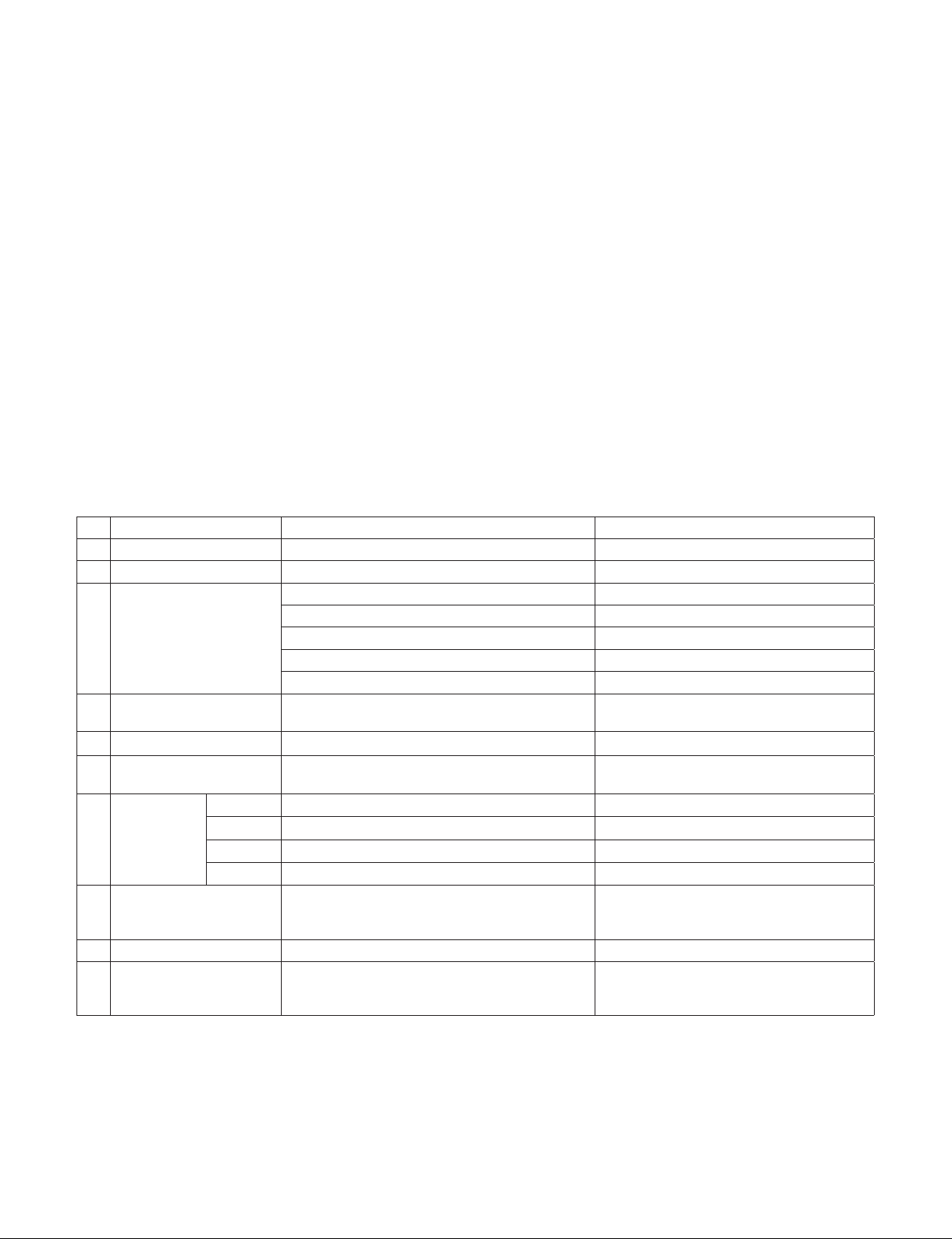
4. General Specification
No Item Specication Remark
1 Market North America
2 Broadcasting system ATSC / NTSC-M, 64 & 256 QAM
3 Available Channel VHF : 02~13
UHF : 14~69
DTV : 02-69
CATV : 01~135
CADTV : 01~135
4 Receiving system Digital : ATSC, 64 & 256 QAM
Analog : NTSC-M
5 Video Input NTSC-M Rear gender(1EA)
6 Component Input Y/Cb/Cr, Y/ Pb/Pr Rear gender(1EA),
Rear (1EA) for UJ65
7 HDMI Input HDMI 1 PC / DTV format Side, Support 6Gbps
HDMI 2 PC / DTV format Side, Support 6Gbps, Support ARC
HDMI 3 PC / DTV format Rear, Support 6Gbps
HDMI 4 PC / DTV format Rear, Support 6Gbps Except for UJ63
8 Audio Input Component / AV Audio / DVI Audio L/R Input ; Rear(Gender)
Component and av and DVI use same jack ;
L/R Input ; Rear for UJ65
9 SPDIF out(1EA) Optical Audio out Rear (1EA),
10 USB Input(3EA) EMF, DivX HD, For SVC (download) JPEG, MP3, DivX HD
Side(1EA), Rear(2EA)
Side(1EA), Rear(1EA) for UJ65, UJ63
- 6 -
Page 7
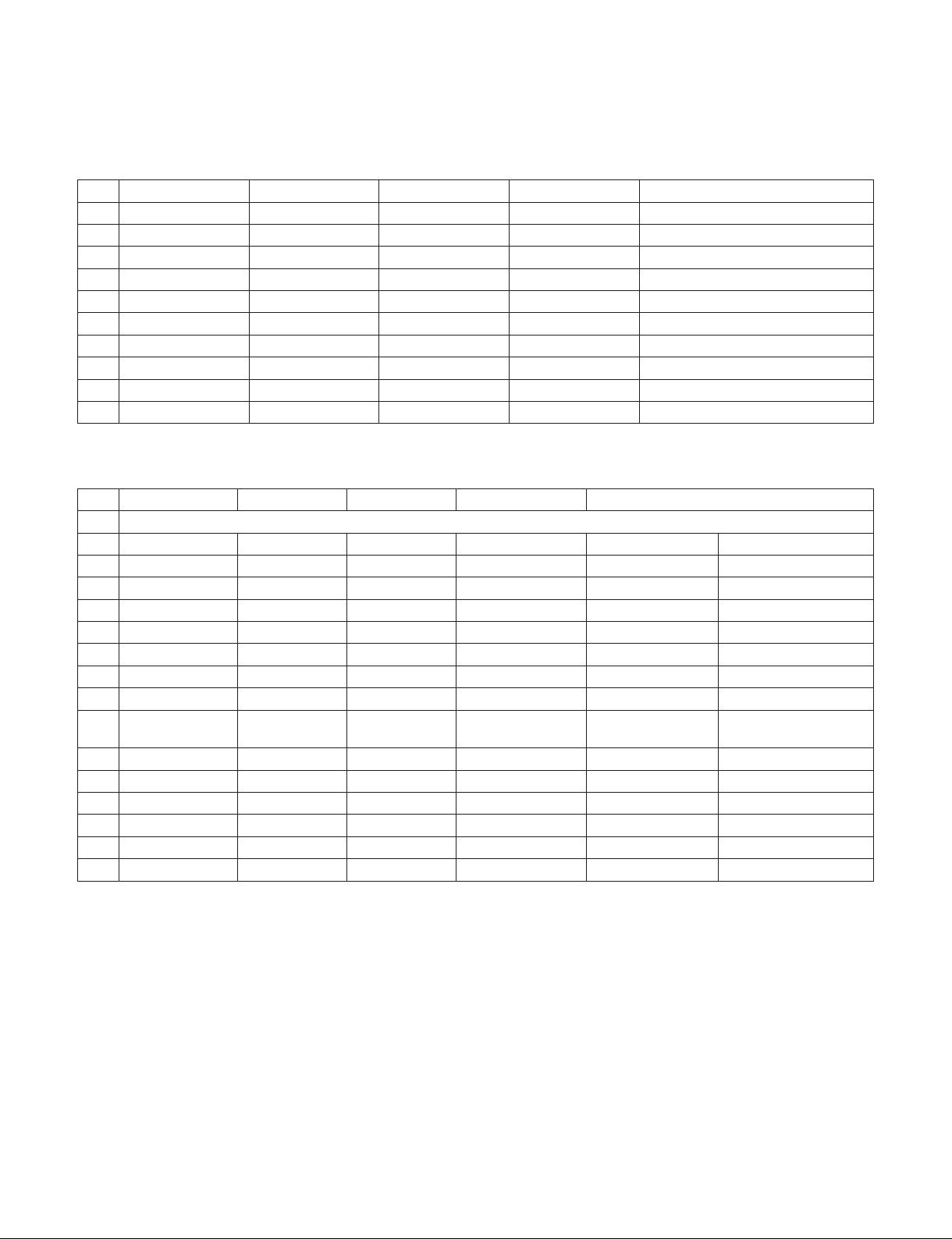
5. External Input Support Format
5.1. Component (Y, CB/PB, CR/PR)
No. Resolution H-freq(kHz) V-freq.(kHz) Pixel clock(MHz) Proposed
1 720*480i 15.73 59.94 13.50 SDTV, DVD 480I(525I)
2 720*480i 15.75 60.00 13.51 SDTV, DVD 480I(525I)
3 720*480p 31.47 59.94 27.00 SDTV 480P
4 720*480p 31.50 60.00 27.02 SDTV 480P
5 1280*720p 44.96 59.94 74.17 HDTV 720P
6 1280*720p 45.00 60.00 74.25 HDTV 720P
7 1920*1080i 33.72 59.94 74.17 HDTV 1080I
8 1920*1080i 33.75 60.00 74.25 HDTV 1080I
9 1920*1080p 67.43 59.94 148.5 HDTV 1080P
10 1920*1080p 67.50 60.00 148.5 HDTV 1080P
5.2. HDMI Input (PC/DTV)
No. Resolution H-freq(kHz) V-freq.(kHz) Pixel clock(MHz) Proposed
HDMI-PC
1 640*350 31.46 70.09 25.17 EGA
2 720*400 31.46 70.08 28.32 DOS
3 640*480 31.46 59.94 25.17 VESA(VGA)
4 800*600 37.87 60.31 40 VESA(SVGA)
5 1024*768 48.36 60.00 65 VESA(XGA)
6 1360*768 47.71 60.01 84.75 VESA(WXGA)
7 1152*864 54.34 60.05 80 VESA
8 1280*1024 63.98 60.02 109.00 SXGA Support to HDMI-PC
9 1920*1080 67.5 60 158.40 WUXGA
(Reduced Blanking)
10 1920*1080 135 120 297 UDTV 1080P
11 3840*2160 54 24.00 297.00 UDTV 2160P
12 3840*2160 56.25 25.00 297.00 UDTV 2160P
13 3840*2160 67.5 30.00 297.00 UDTV 2160P
14 4096*2160 53.95 23.97 296.70 UDTV 2160P
15 4096*2160 54 24 297 UDTV 2160P
- 7 -
Page 8
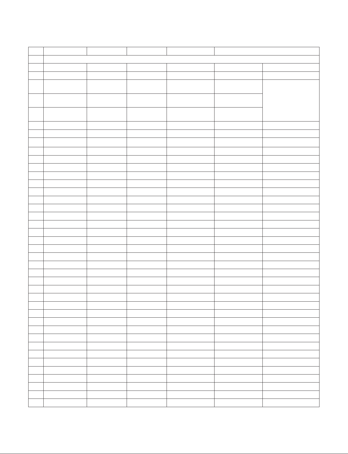
No. Resolution H-freq(kHz) V-freq.(kHz) Pixel clock(MHz) Proposed
DTV
1 640*480 31.46 59.94 25.12 SDTV 480P
2 640*480 31.5 60.00 25.12 SDTV 480P
3 720*480 15.73 59.94 13.50 SDTV, DVD
480I(525I)
4 720*480 15.75 60.00 13.51 SDTV, DVD
480I(525I)
5 720*576 15.62 50.00 13.50 SDTV, DVD
576I(625I) 50Hz
6 720*480 31.47 59.94 27 SDTV 480P
7 720*480 31.5 60.00 27.02 SDTV 480P
8 720*576 31.25 50.00 27 SDTV 576P
9 1280*720 44.96 59.94 74.17 HDTV 720P
10 1280*720 45 60.00 74.25 HDTV 720P
11 1280*720 37.5 50.00 74.25 HDTV 720P
12 1920*1080i 28.12 50.00 74.25 HDTV 1080I
13 1920*1080i 33.72 59.94 74.17 HDTV 1080I
14 1920*1080i 33.75 60.00 74.25 HDTV 1080I
15 1920*1080p 26.97 23.97 63.29 HDTV 1080P
16 1920*1080p 27.00 24.00 63.36 HDTV 1080P
17 1920*1080p 33.71 29.97 79.120 HDTV 1080P
18 1920*1080p 33.75 30.00 79.20 HDTV 1080P
19 1920*1080p 56.25 50.00 148.5 HDTV 1080P
20 1920*1080p 67.43 59.94 148.35 HDTV 1080P
21 1920*1080p 67.5 60.00 148.50 HDTV 1080P
22 1920*1080p 112.5 100 297.00 UDTV 1080P
23 1920*1080p 134.86 119.88 296.70 UDTV 1080P
24 1920*1080p 135.00 120 297 UDTV 1080P
25 3840*2160p 53.95 23.98 296.70 UDTV 2160P
26 3840*2160p 54 24.00 297.00 UDTV 2160P
27 3840*2160p 56.25 25.00 297.00 UDTV 2160P
28 3840*2160p 61.43 29.97 296.70 UDTV 2160P
29 3840*2160p 67.5 30.00 297.00 UDTV 2160P
30 3840*2160p 112.5 50.00 594 UDTV 2160P
31 3840*2160p 134.86 59.94 593.40 UDTV 2160P
32 3840*2160p 135 60.00 594 UDTV 2160P
33 4096*2160p 53.95 23.98 296.70 UDTV 2160P
34 4096*2160p 54 24.00 297 UDTV 2160P
35 4096*2160 56.25 25.00 297 UDTV 2160P
36 4096*2160 61.43 29.97 296.70 UDTV 2160P
37 4096*2160 67.5 30.00 297 UDTV 2160P
38 4096*2160 112.5 50.00 594 UDTV 2160P
39 4096*2160 134.86 59.94 593.40 UDTV 2160P
40 4096*2160 135 60.00 594 UDTV 2160P
Spec. out but display
- 8 -
Page 9
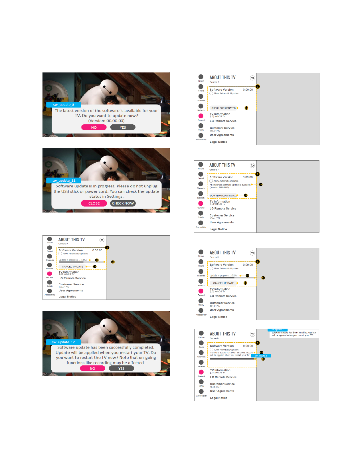
SOFTWARE UPDATE
1. USB
(1) Insert the USB memory Stick to the USB port
(2) Automatically detect the SW Version and show the below
message
(3) Click [YES]: initiate the download and install of the update.
2. NSU
(This Function is needed to connect to the internet)
(1) Menu -> All Settings -> General -> About This TV
(2) Click [CHEK FOR UPDATES] : system check newest
version
(4) Click [Check Now]: move to “About This TV” page for
update
(5) TV is updating
(6) After finished the update, below Pop-up appear
(7) Click [Yes] : TV will be DC OFF -> ON
(8) After TV turned on, Check the updated SW Version and
Tool Option
(3) Click [DOWNLOAD AND INSTALL]
(4) TV is updating
(5) After finished the update, below Pop-up appear
(6) Turn OFF the TV and On. Check the updated SW Version
and Tool Option
- 9 -
Page 10
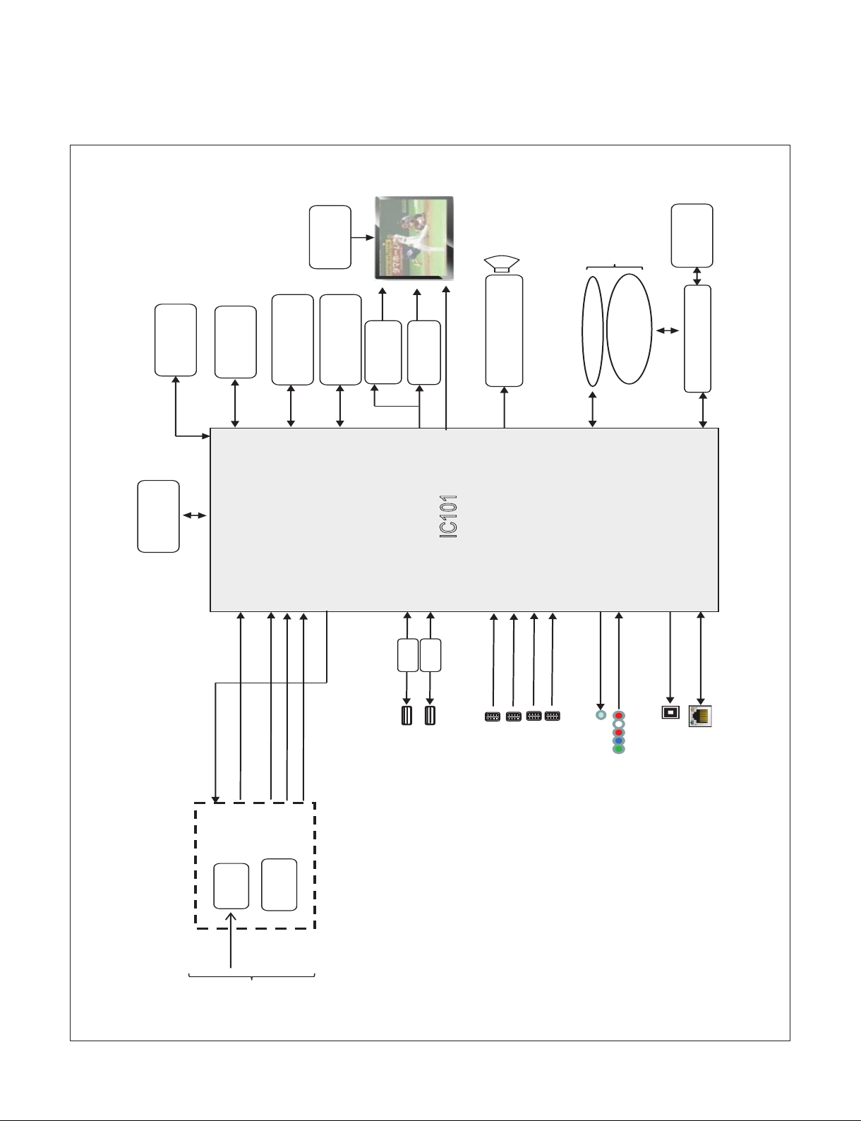
1. Main IC
MAIN Audio AMP
IC5800
IC101
IF+, IF-
OPTIC
LAN
HDMI1 HDMI 2.0
EEPROM(NVRAM)
(256Kb) IC102
PHY3_RX0N
Air/
Cable
TUNER
(C/A )
DEMOD
USB1 (2.0)
eMMC IC8800
(4GB)
Sub Micom (IC3000)
P_TS
X_TAL
24MHz
X_TAL
32.768KHz
I2S Out
I2C 0
I2C 4
R
E
A
R
YPbPr
SPDIF OUT
ETHERNET
I2C 1
SUB
ASSY
IR / KEY
LOGO LIGHT(Ready)
WIFI/BT Combo
USB_WIFI
CVBS
HDMI3 HDMI 2.0
USB2 (2.0)
RS232C/HP
HDMI2(ARC) HDMI 2.0
AV
EPI 3G/1.5G
OCP
OCP
USB2.0_2_DM1
USB2.0_3_DM0
PHY2_RX0N
PHY1_RX0N
I2C6
SIF
HDMI4 HDMI 2.0
PHY0_RX0N
PMIC
(IC9200)
GAMMA IC
(IC9400)
CVBS/COMP
M0
M1
DDR3 2133
512MB
DDR3 2133
256MB
I2C
5
Sub PMIC
(IC9300)
BLOCK DIAGRAM
- 10 -
Page 11
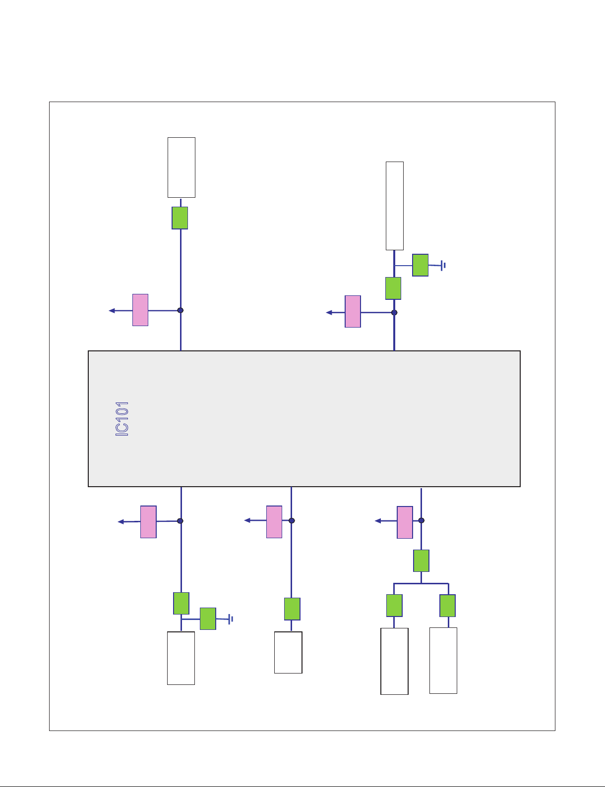
2. I2C
SCL0
SDA0
100Ω
3.3KΩ
IC101
+3.3V_NORMAL
3.3KΩ
33Ω
IC102
EEPROM
+3.3V_NORMAL
IC5800
AUDIO AMP
SCL2
SDA2
TUNER
SCL4
SDA4
33pF
SCL5
SDA5
1.8KΩ
SCL1
SDA1
IC3000
MICOM
33Ω
3.3KΩ
+3.3V_NORMAL
3.3KΩ
+3.3V_NORMAL
IC9200
PMIC
33Ω
IC9400
GAMMA IC
33Ω
33Ω
33Ω
47pF
+3.3V_TU
- 11 -
Page 12
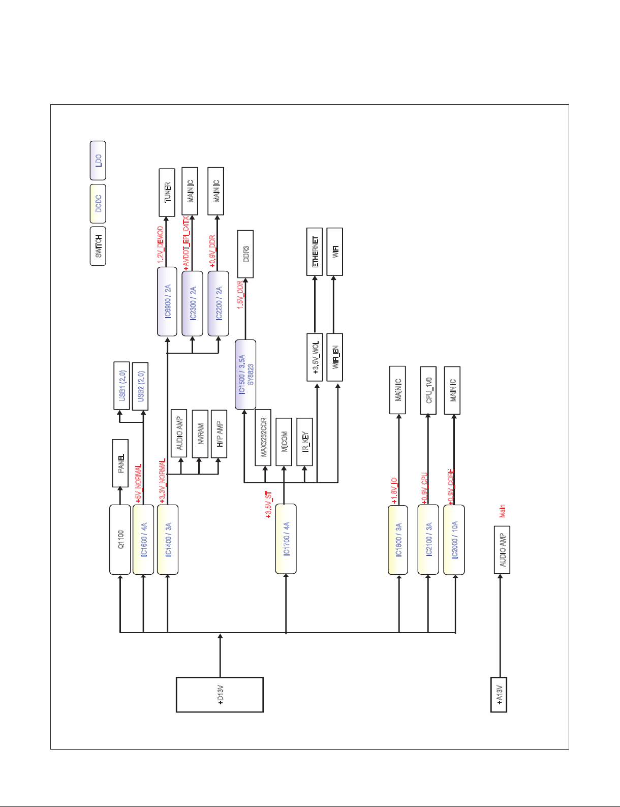
3. Power
LDO DCDC
+
D13V
+5V_NORMAL
IC1600 / 4A
IC1400 / 3A
Q1100
IC1700 / 4A
AUDIO AMP
DDR3
+
3.3V_NORMAL
+3. 5V_ST
+1.8V_IO
IC2100 / 3A
+0.9V_CPU
IC2000 / 10A
+0.9V_CORE
+A13V
USB1 (2.0)
USB2 (2.0)
PANEL
IC1500 / 3. 5A
S
Y8823
1.5V_DDR
MICOM
IR_KEY
ETHERNET
WIFI
+3.5V_WOL
WIFI_EN
CPU_1V0
MAIN IC
Main
IC6900 / 2A
IC1800 / 3A
SWITCH
+0. 9V_DDR
MAIN IC
NVRAM
H/ P AMP
1.2V_DEMOD
TUNER
AUDIO AMP
MAX3232CDR
IC2200 / 2A
IC2300 / 2A
+AVDDT_EPI_C4TX
MAIN IC
MAIN IC
- 12 -
Page 13
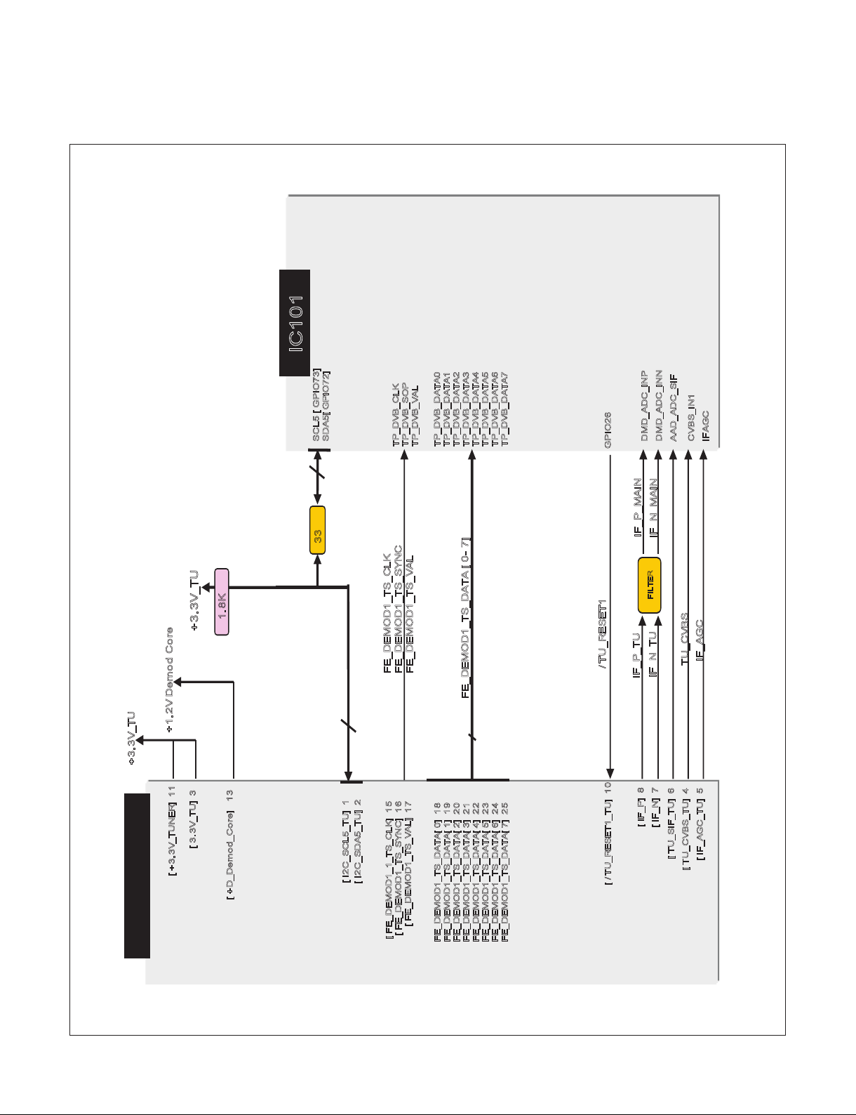
4. Tuner
SCL5 [ GPIO73]
S
DA5[ GPIO72]
D
MD_ADC_INP DMD_ADC_INN
A
AD_ADC_SIF
[ +3.3V_TUNER] 11
[
IF_P] 8
[
IF_N] 7
[
FE_DEMOD1_1_TS_CLK] 15
[
FE_DEMOD1_TS_SYNC] 16
[
FE_DEMOD1_TS_VAL] 17
F
E_DEMOD1_TS_DATA[ 0] 18 FE_DEMOD1_TS_DATA[ 1] 19 FE_DEMOD1_TS_DATA[ 2] 20 FE_DEMOD1_TS_DATA[ 3] 21 FE_DEMOD1_TS_DATA[ 4] 22 FE_DEMOD1_TS_DATA[ 5] 23 FE_DEMOD1_TS_DATA[ 6] 24 FE_DEMOD1_TS_DATA[ 7] 25
+3. 3V_TU
[ I2C_SCL5_TU] 1
[
I2C_SDA5_TU] 2
[
TU_SIF_TU] 6
[
TU_CVBS_TU] 4
[
IF_AGC_TU] 5
[
/ TU_RESET1_TU] 10
FILTER
FE_DEMOD1_TS_CLK
F
E_DEMOD1_TS_SYNC FE_DEMOD1_TS_VAL
F
E_DEMOD1_TS_DATA [ 0- 7]
33 Ω
IF_P_TU
I
F_N_TU
T
U_CVBS
I
F_AGC
I
F_P_MAIN
I
F_N_MAIN
/ TU_RESET1
GPIO26
C
VBS_IN1
I
FAGC
+3.3V_TU
1.8 KΩ
IC101
TP_DVB_CLK
T
P_DVB_SOP TP_DVB_VAL TP_DVB_DATA0 TP_DVB_DATA1 TP_DVB_DATA2 TP_DVB_DATA3 TP_DVB_DATA4 TP_DVB_DATA5 TP_DVB_DATA6 TP_DVB_DATA7
[
3.3V_TU] 3
[ +D_Demod_Core] 13
+1. 2V Demod Core
TUNER
- 13 -
Page 14

5. Video/Audio
IC101
CVBS_IN2
Tuner
Jack Side
SoC Side
JK3400
AV_CVBS_IN
COMP2_Pb
COMP2_Pr
COMP2/AV_L_IN
COMP2/AV_R_IN
AV1_CVBS_IN_SOC
COMP2_Pb_IN_SOC
COMP2_Pr_IN_SOC
AUAD_L_CH2_IN
AUAD_L_CH2_IN
AUAD_R_CH2_IN
TU_CVBS_TU
TU_SIF_TU, IF_P/N_TU
CVBS_IN1
AAD_ADC_SIF, DMD_ADC_INP, DMD_ADC_INN
TU_CVBS
TU_SIF, IF_P/N
FE_DEMOD1/2_TS_CLK,SYNC,VAL
FE_DEMOD1/2_TS_CLK,SYNC,VAL
[TP0CLK ,VLD,SYNC]
AUAD_R_CH2_IN
VIN3P
VIN5P
COMP2_Y
Y1_IN
COMP2_Y_IN_SOC
- 14 -
Page 15
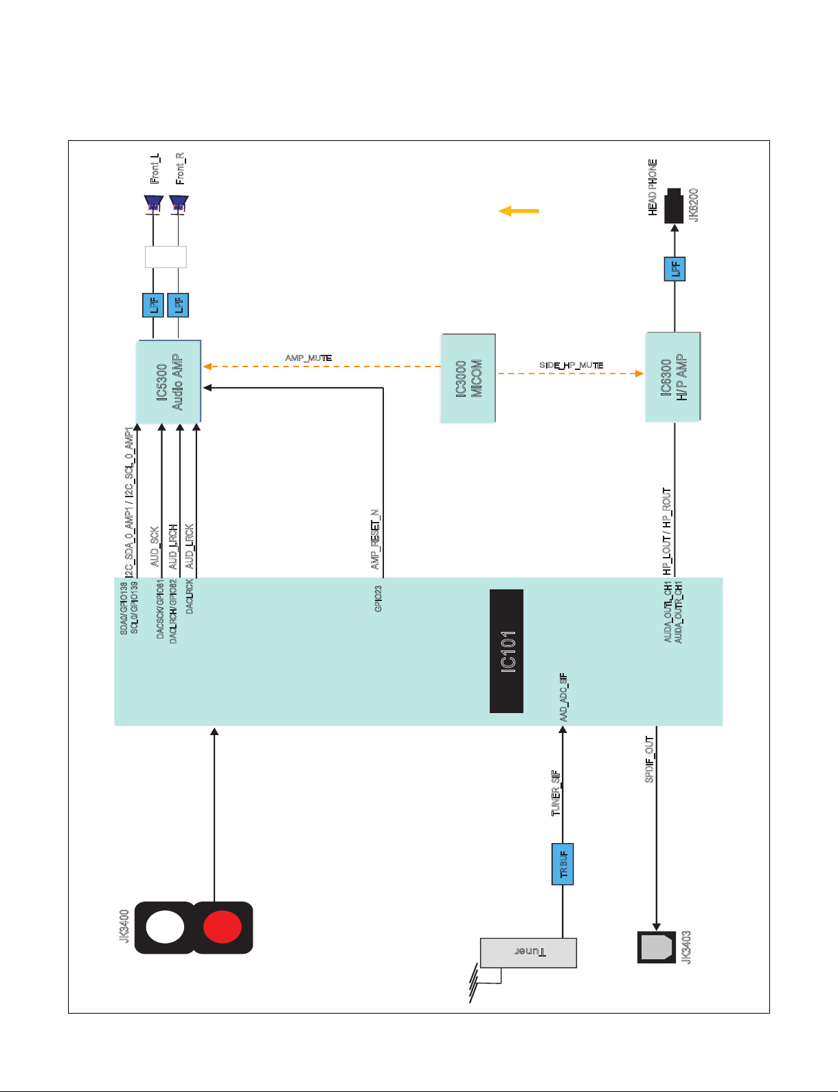
SPDIF_OUT
IC5300
A
udio AMP
LPF
IEC958OUT
Tune
r
TR BUF
A
AD_ADC_SIF
HP_LOUT / HP_ROUT
H
EAD PHONE
LPF
AUDA_OUTL_CH1
A
UDA_OUTR_CH1
TUNER_SIF
IC3000
MICOM
AMP_MUT
E
GPIO23
AMP_RESET_N
JK3403
JK6200
LPF
Front_L
Front_R
DACSCK/ GPIO81
IC101
JK3400
COMP2/AV_R_IN
COMP2/AV_L_IN
AUAD_R_CH1_IN
AUAD_L_CH2_IN
SDA0/GPIO138
S
CL0/ GPIO139
AUD_LRCK
A
UD_LRCH
IC6300
H/ P AMP
I2C_SDA_0_AMP1 / I2C_SCL_0_AMP1
DACLRCH/ GPIO82
D
ACLRCK
AUD_SCK
S
IDE_HP_MUTE
6. I2C Map
- 15 -
Page 16
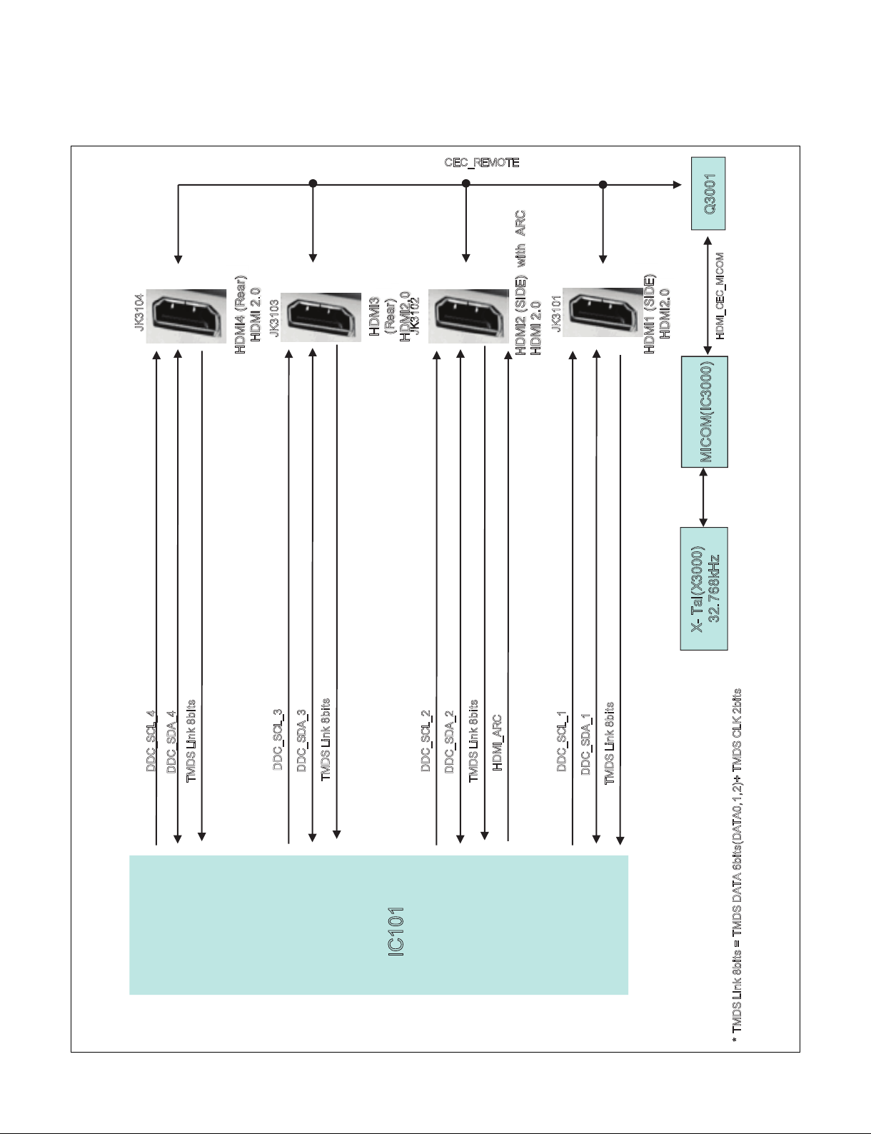
HDMI4 (Rear)
H
DMI 2.0
HDMI2 (SIDE) with ARC
H
DMI 2.0
C
EC_RE
MOTE
MICOM(IC3000)
I
C101
HDMI_ARC
X- Tal(X3000)
3
2.768kHz
HDMI1 (SIDE)
H
DMI2.0
DDC_SCL_1
D
DC_SDA_1
T
MDS Link 8b its
DDC_SCL_2
D
DC_SDA_2
T
MDS Link 8b its
DDC_SCL_4
D
DC_SDA_4
* TMDS Link 8bits = TMDS DATA 6bits(DATA0,1,2)+ TMDS CLK 2bits
TMDS Link 8bits
HDMI_CEC_MICOM
Q3001
DDC_SCL_1
DDC_SDA_1
J
K3104
J
K3102
J
K3101
HDMI3
(
Rear)
H
DMI2.0
JK3103
DDC_SCL_3
D
DC_SDA_3
T
MDS Link 8b its
DDC_SCL_2
DDC_SDA_2
PHY0_ARC_OUT
DDC_SCL_3
DDC_SDA_3
DDC_SCL_4
DDC_SDA_4
7. EPI block (PMIC)
- 16 -
Page 17
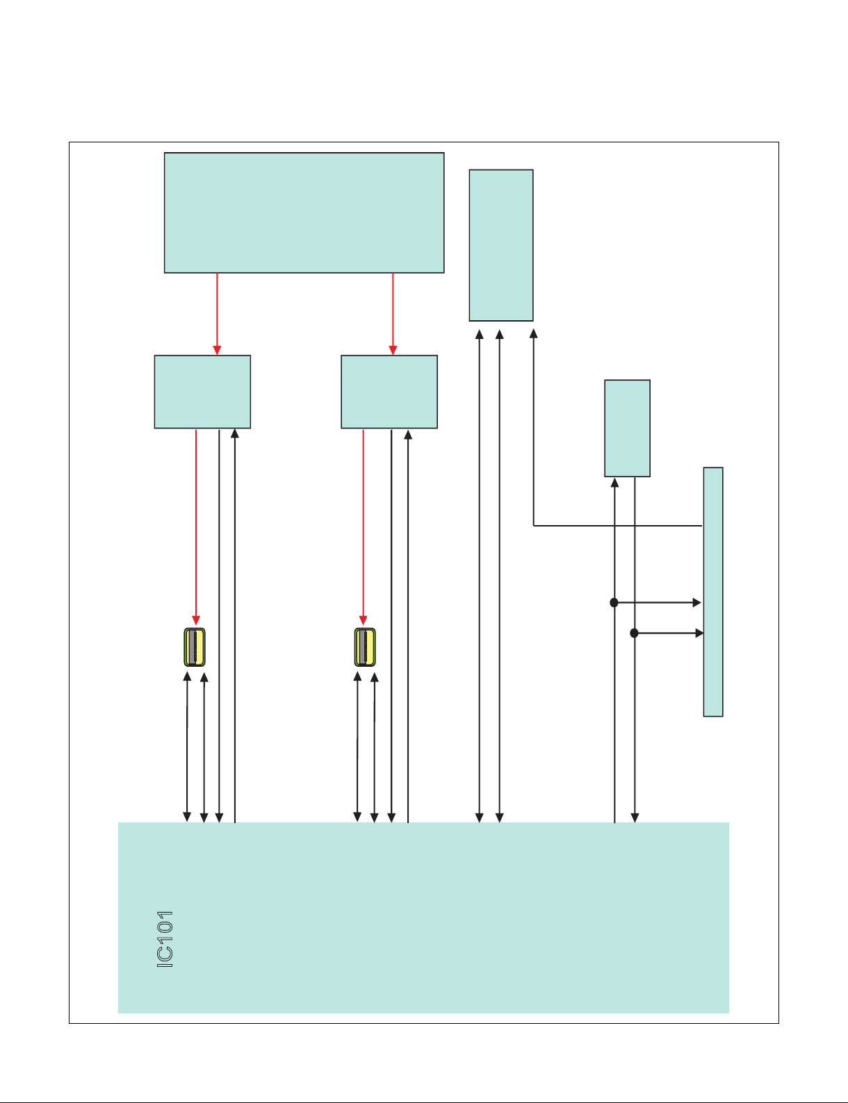
USB2(REAR)
USB2.0_2_DP1
USB2.0_2_DM1
GPIO94
GPIO95
USB2_0_DM0
USB2_0_DP0
USB1(SIDE)
USB2.0_2_DP1
USB2.0_2_DM1
IC1600
5V / 4A
+5V_USB_3
+5V_USB_2
/USB_OCD2
USB_CTL2
USB_CTL2
/USB_OCD2
WIFI_DM
WIFI_DP
USB2_2_DM0
USB2_2_DP0
MICOM(IC3000)
UART0_TXD/GPIO105
UART0_RXD/GPIO106
SOC_TX
SOC_RX
IC7200
USB2.0
WIFI Combo
BT_RESET
BT_WAKEUP_DEVICE
BT_WAKEUP_HOST
OCP
IC4700
OCP
IC4501
+5V_NORMAL
+5V_NORMAL
JK4400
JK4600
USB2.0
IC101
USB2_1_DM0
USB2_1_DP0
SPI_CS1/GPIO32
SPI_DI1/GPIO35
8. USB / WIFI / M-REMOTE / UART
- 17 -
Page 18
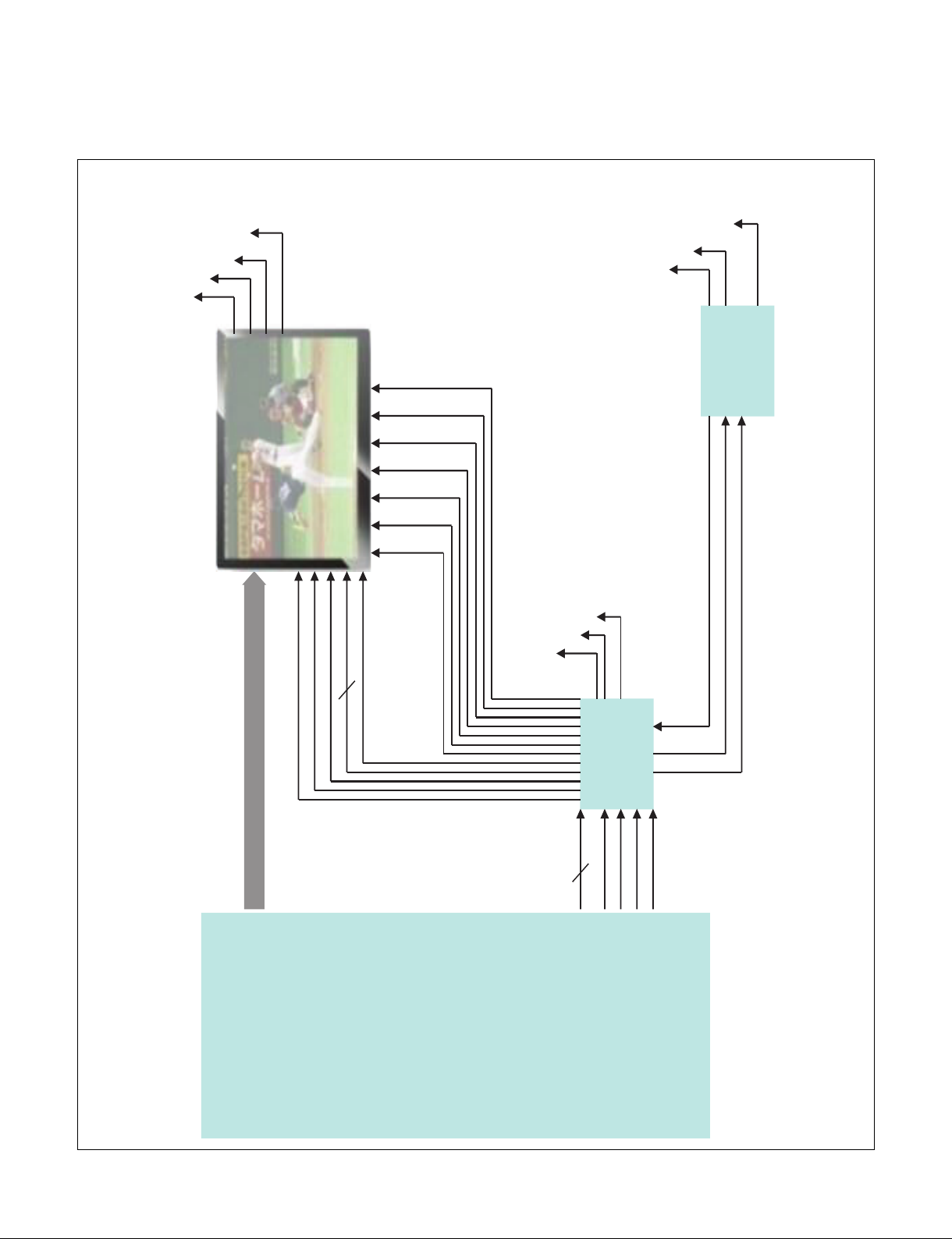
TX 6 lane
IC101
PMIC
IC9200
Boost IC
IC9300
VCORE
VCC18
HVDD
VDD_EPI
VCOM1
VCOMLFB
VCOM2
VGL1
VST
GIP_RST
LS_VGL
VGH_EVEN
VGH_ODD
VGH
10
CLK[1:10]
GMA1,4,5,6,9,10,13,14,15,18
10
PM_VCC
SDA2/GPIO78
SCL2/GPIO79
I2C_SDA_BACKEND
I2C_SCL_BACKEND
VDD_EPI
VCORE
SWG
SWO
SWI
PM_VCC
VCC18
PANEL_VCC
E0
GST
MCLK
GCLK
PANEL_VCC
9. LGD 60Pin Interface
- 18 -
Page 19
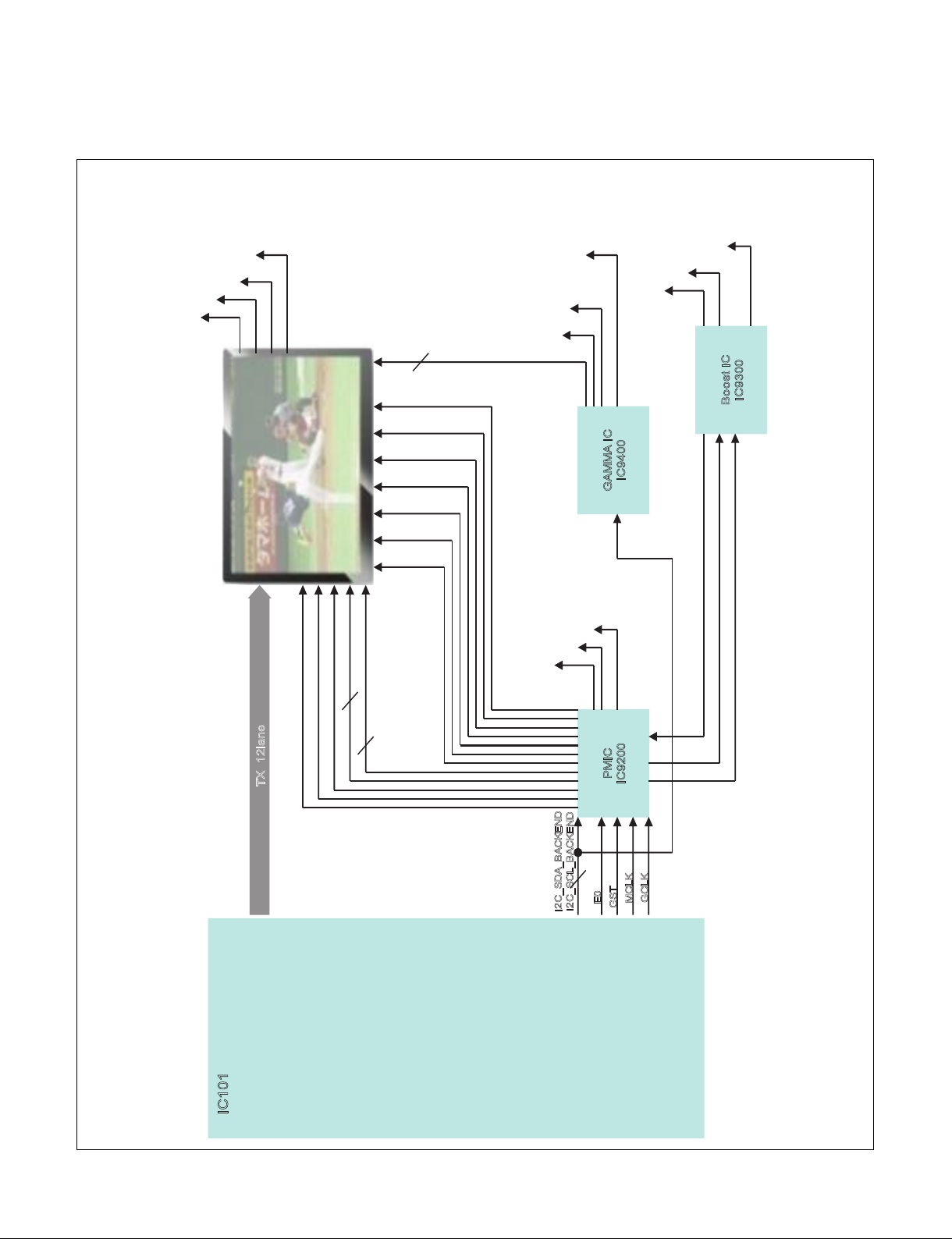
TX 12lane
IC101
PMIC
IC9200
Boost IC
I
C9300
VCORE
VCC18
HVDD
VDD_EPI
VCOM1
VCOMLFB
VCOM2
VGL1
VST
GIP_RST
LS_VGL
VGH_EVEN
VGH_ODD
VGH
6
CLK[1:6]
GMA1,5,6,,9,10,13,14,18
8
GMA2,3,4,7,8,11,12,15,16,1
7
SDA2/GPIO78
SCL2/GPIO79
I2C_SDA_BACKEND
I
2C_SCL_BACKEND
VDD_EPI
VCORE
SWG
SWO
SWI
PM_VCC
VCC1
8
PANEL_VCC
E0
GST
MCLK
G
CLK
GAMMA IC
IC9400
10
HVDD
VDD_EPI
3.3V_NORMAL
PM_VCC
PANEL_VCC
10. BOE 68Pin Interface
- 19 -
Page 20
200
400
800
540
521
120
820
LV1
530
901
902
121
AR1
700
A10
500
570
571
LV2
ARC1
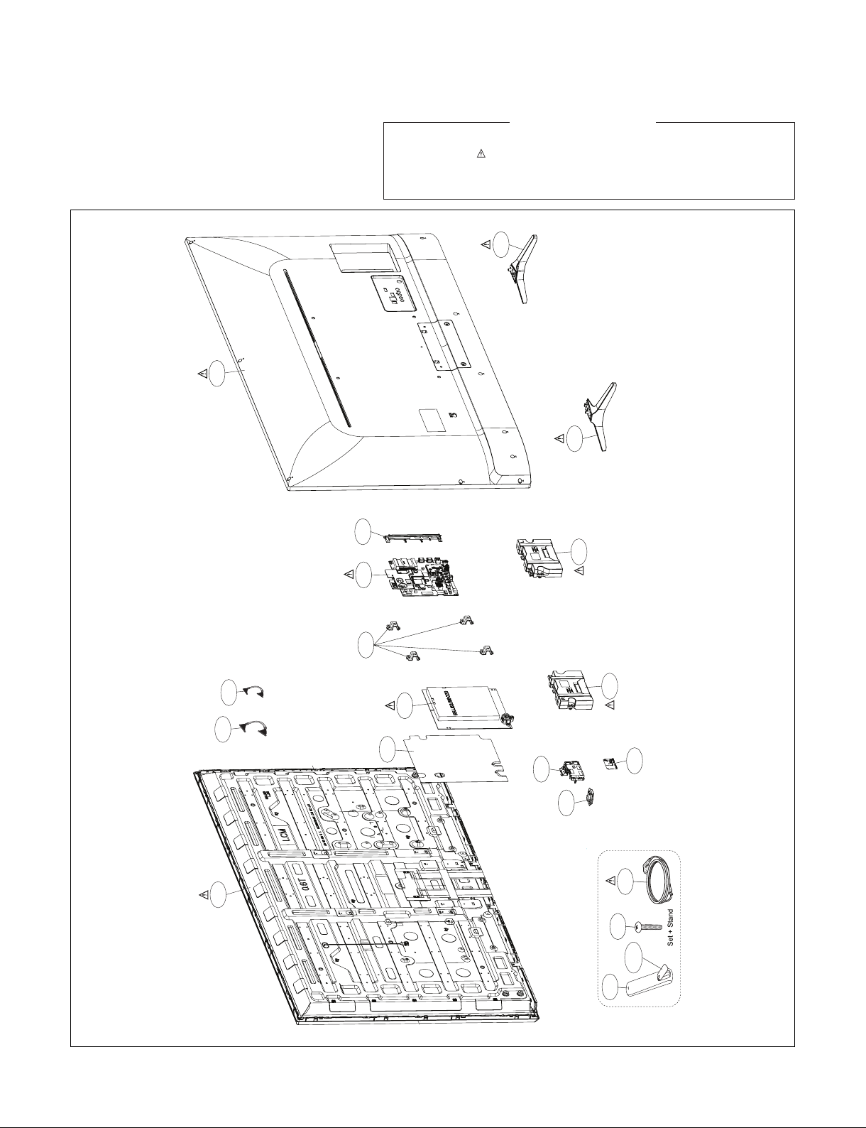
EXPLODED VIEW
IMPORTANT SAFETY NOTICE
Many electrical and mechanical parts in this chassis have special safety-related characteristics. These
parts are identified by in the EXPLODED VIEW.
It is essential that these special safety parts should be replaced with the same components as
recommended in this manual to prevent Shock, Fire, or other Hazards.
Do not modify the original design without permission of manufacturer.
- 20 -
Page 21
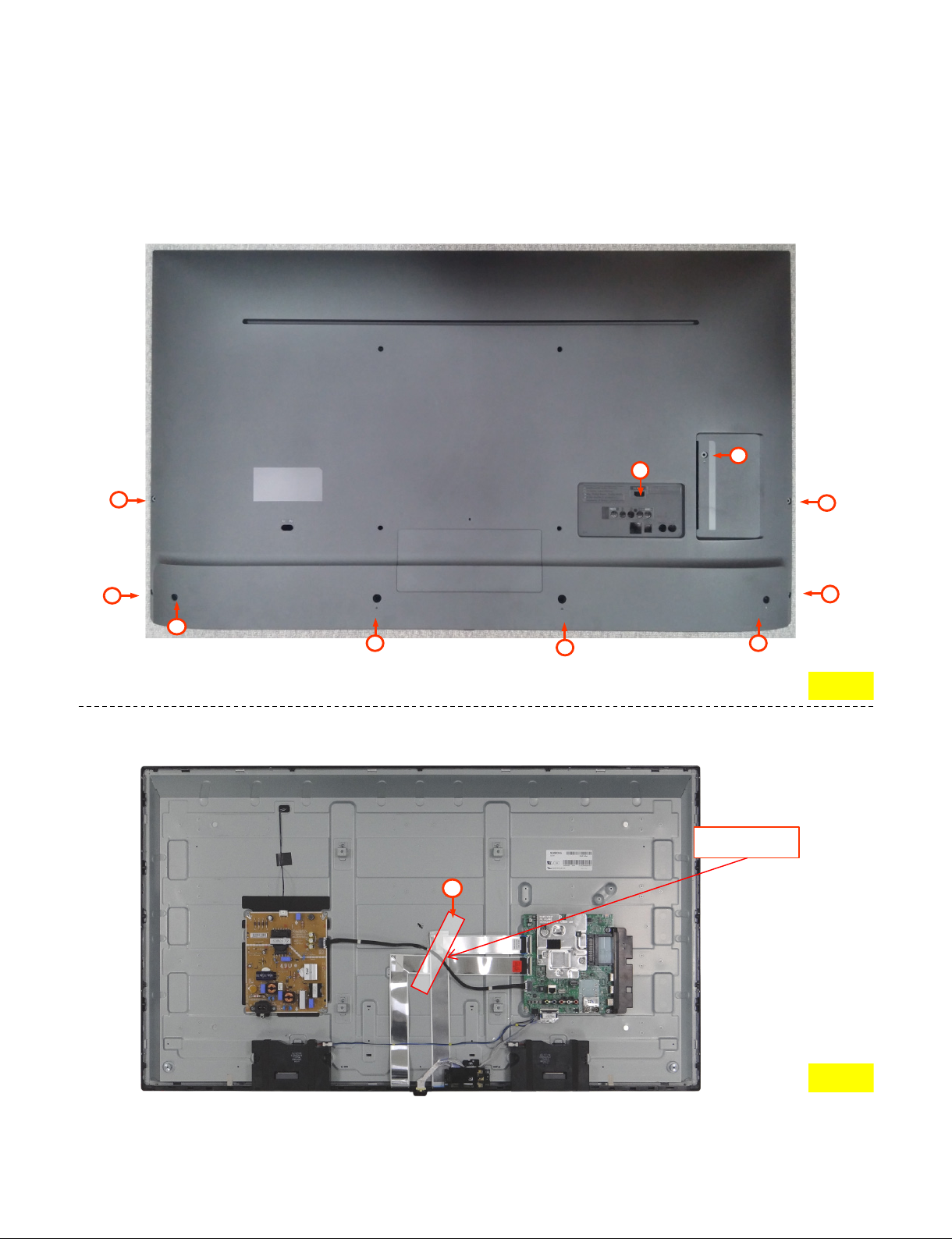
[Fig.1]
[Fig.2]
Screw : 15 ea
2. Detach Tape
Total Screw No.: 10ea
1. After Screw Disassemble,
please remove B/C from Module
Detach tape
2
3
1
3
2
2
2
3
3
3
4
DISASSEMBLY GUIDE
- 21 -
Page 22
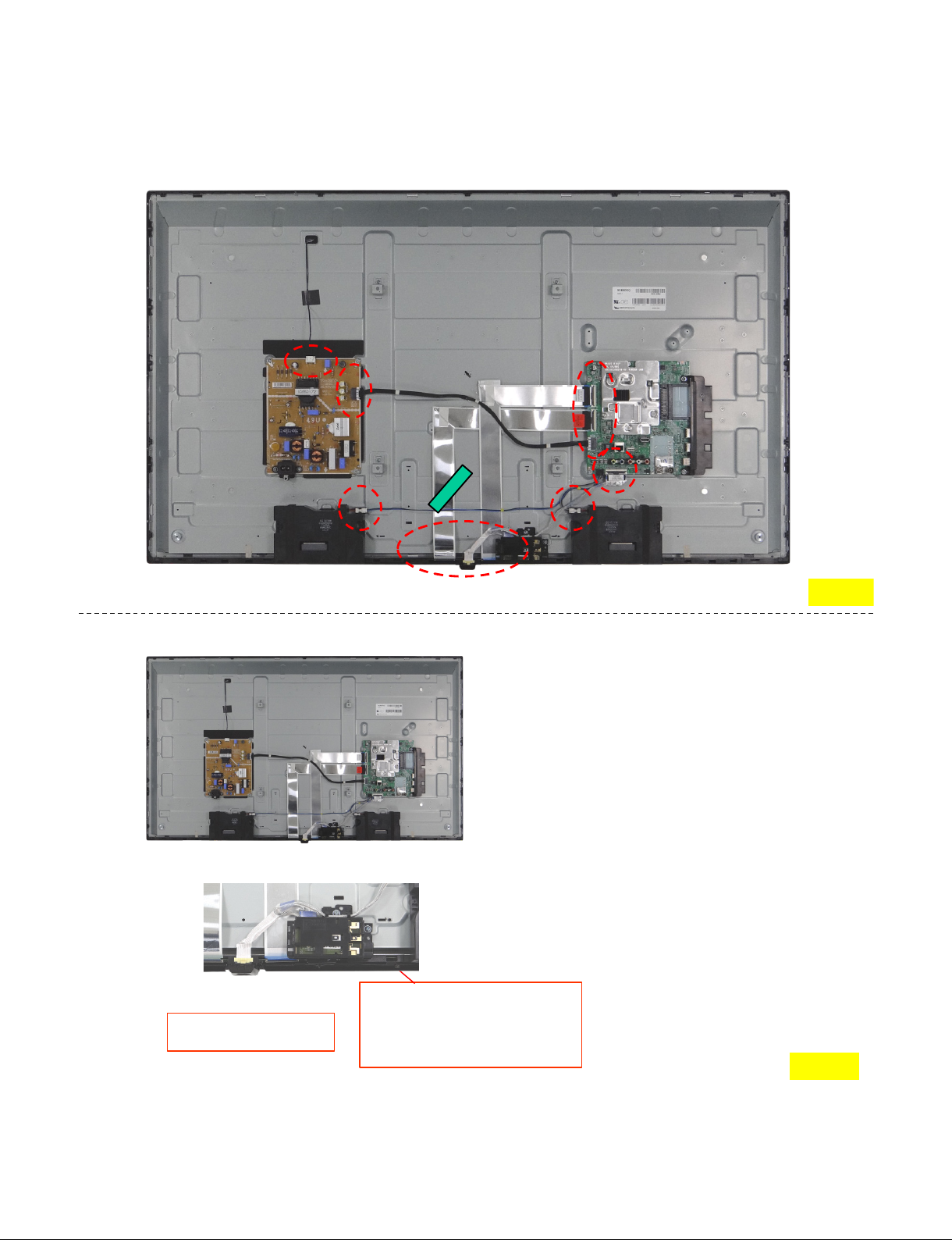
3. Remove all sort of cable
4. IR assy, WiFi PCB assy disassembly
[Fig.3]
[Fig. 4]
Disassemb le screw (1ea) and
Remo ve wi-fi cable
Remove IR cab le
- 22 -
Page 23
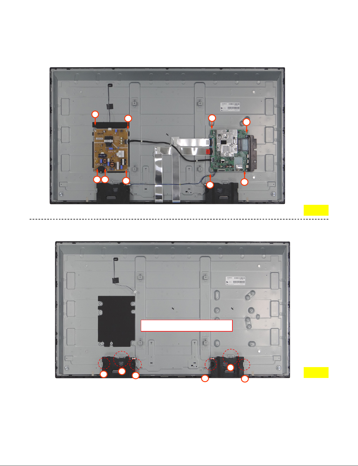
[Fig.7]
[Fig.6]
Screw : 9 ea
5. Screw disassembly
6. Speaker disassembly
2
111
1
1
2
1
1
a
b
b
a
b
b
(Disassemble ⓑ→ⓐ)
- 23 -
Page 24
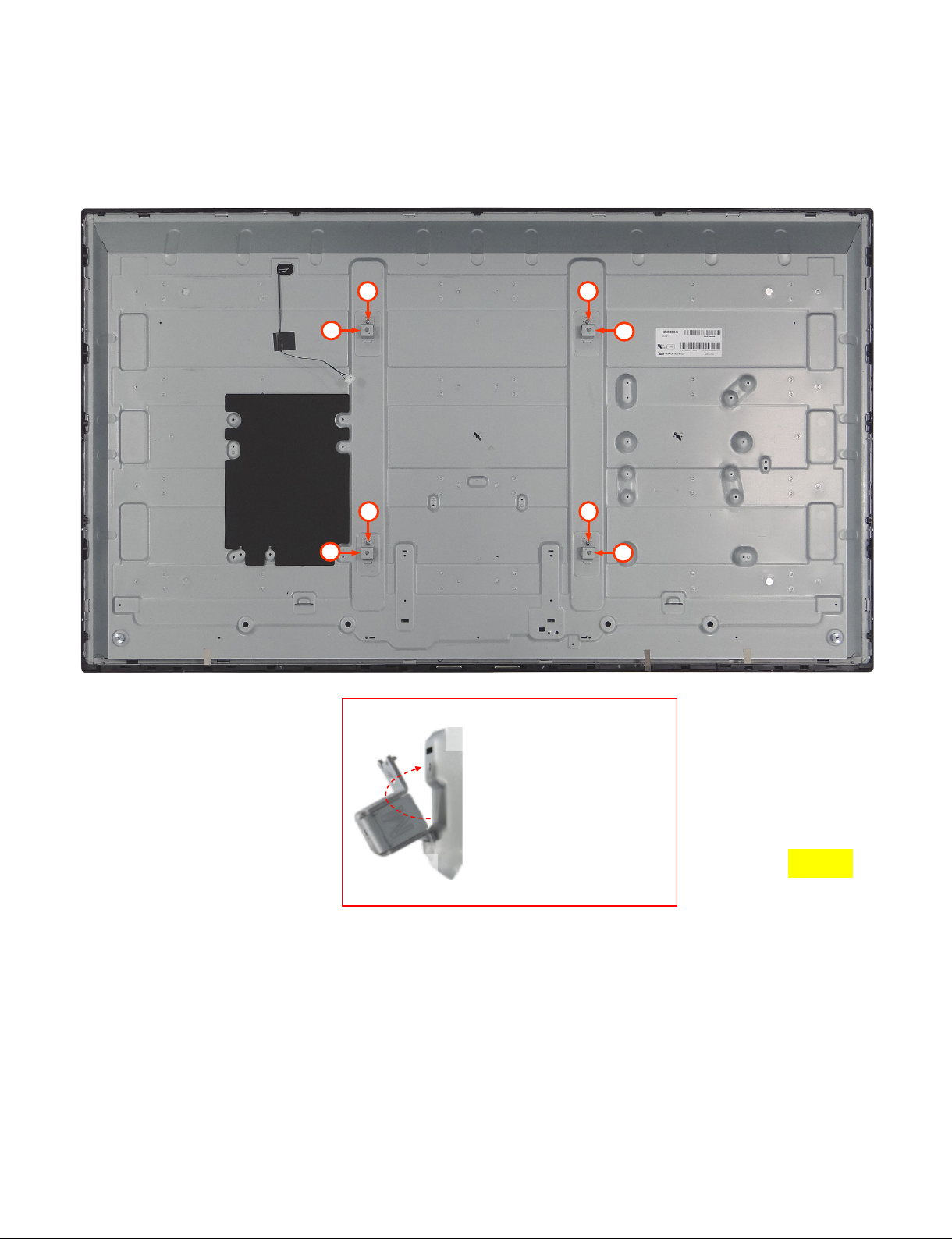
[Fig.8]
Screw : 4ea
8. Screw disassembly
2 2
2 2
1
1
1
1
ⓐ
Disassemb le squenc e
ⓐ→ⓑ)
ⓑ
- 24 -
Page 25

TROUBLE SHOOTING GUIDE
Page 26
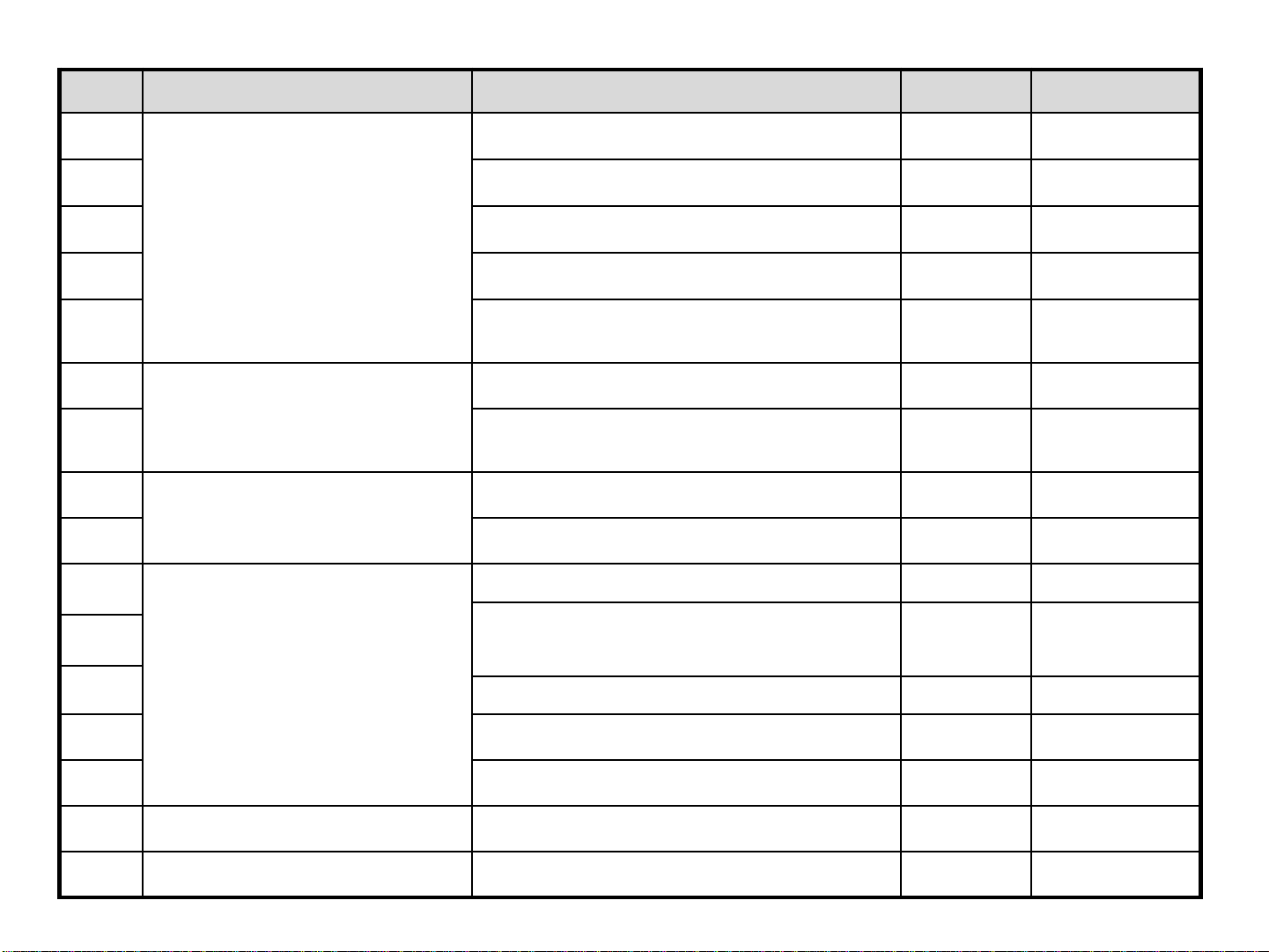
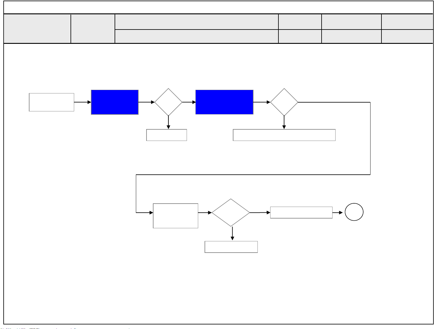
Contents of Standard Repair Process
No. Error symptom (High category) Error symptom (Mid category) Page Remarks
1
2 No video/No audio 2
3 Picture broken/ Freezing 3
4 Color error 4
5
6
7
8
9 Wrecked audio/discontinuation/noise 9
10
11
A. Video error
B. Power error
C. Audio error
No video/Normal audio 1
Vertical/Horizontal bar, residual image,
light spot, external device color error
No power 6
Off when on, off while viewing, power
auto on/off
No audio/Normal video 8
Remote control & Local switch checking
MR15 operating checking 11
10
5
7
12
13 Camera operating checking 13
14 External device recognition error 14
15 E. Noise Circuit noise, mechanical noise 15
16 F. Exterior error Exterior defect 16
D. Function error
Wifi operating checking 12
First of all, Check whether there is SVC Bulletin in GSCS System for these model.
Page 27
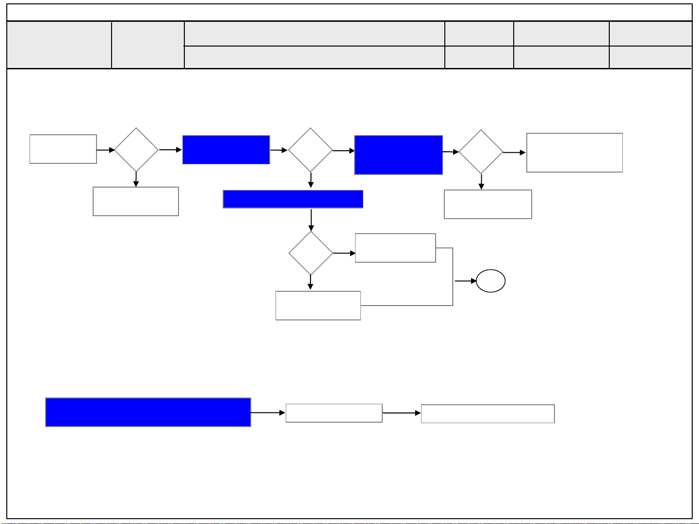
Standard Repair Process
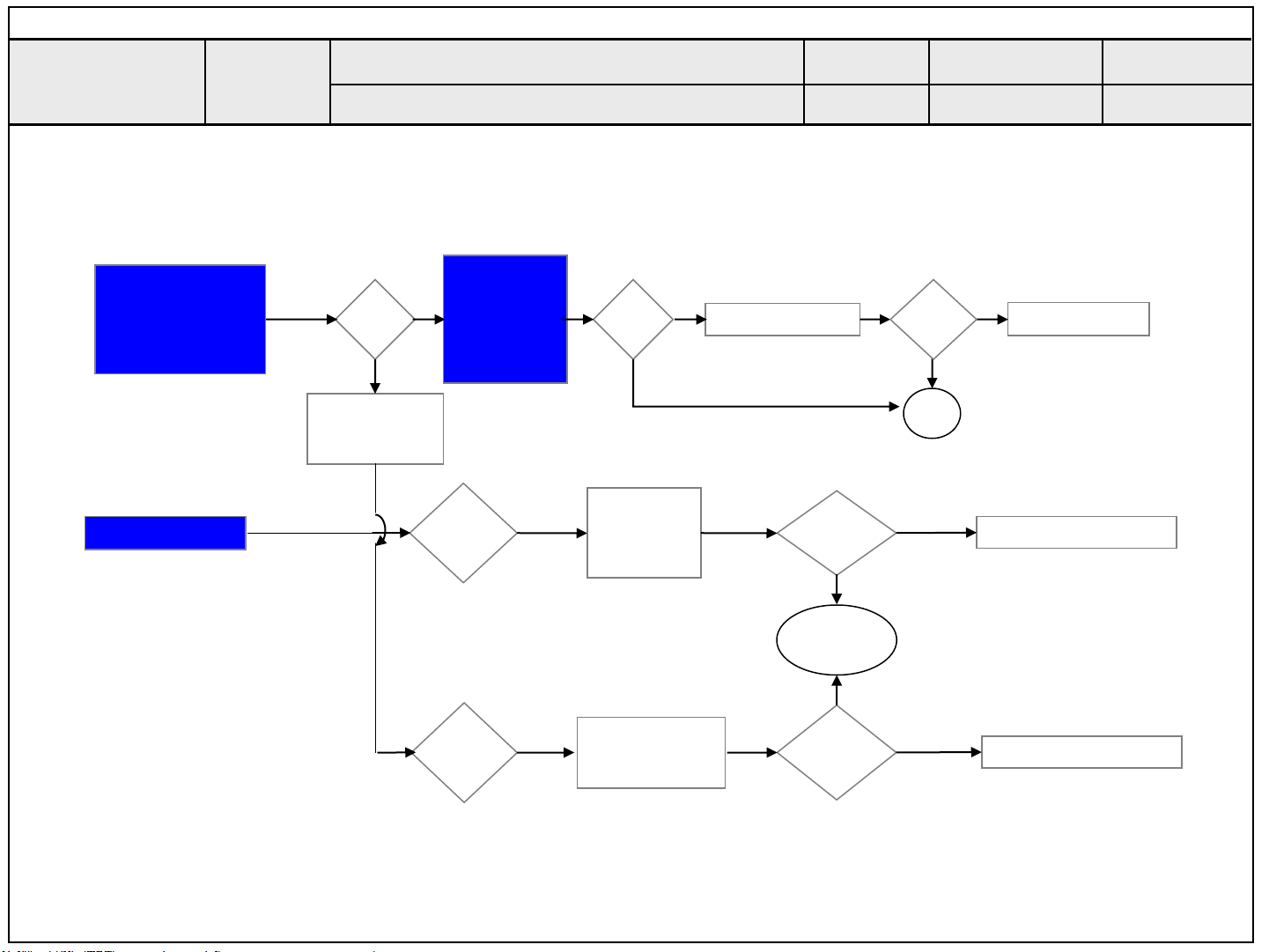
symptom
Error
A. Video error
No video/ Normal audio
Established
date
Revised date
First of all, Check whether all of cables between board is inserted properly or not.
(Main B/D↔ Power B/D, LVDS Cable, Speaker Cable, IR B/D Cable,,,)
☞A18 ☞A1
No video
Normal audio
Normal
audio
N
Move to No
video/No audio
Y
Check Back Light
On with naked eye
☞A18
On
Check Power Board 13V output
Normal
voltage
Repair Power
Board or parts
Y N Check Power
Y
N
Board
13V
Replace Inverter
or module
Normal
voltage
N
Repair Power
Board or parts
End
Replace T-con/Main
Y
Board or module
1/16
※Precaution
Always check & record S/W Version and White
Balance value before replacing the Main Board
☞A4 & A2
Replace Main Board
1
Re-enter White Balance value
Page 28
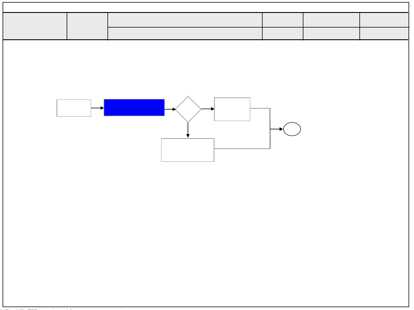
Standard Repair Process
symptom
Error
A. Video error
No video/ No audio
Established
date
Revised date
2/16
☞A18
No Video/
No audio
Check voltage of
Power Board ( 13V…)
Normal
voltage?
N
Replace Power
Board and repair
parts
Y
Check and
replace
MAIN B/D
End
2
Page 29
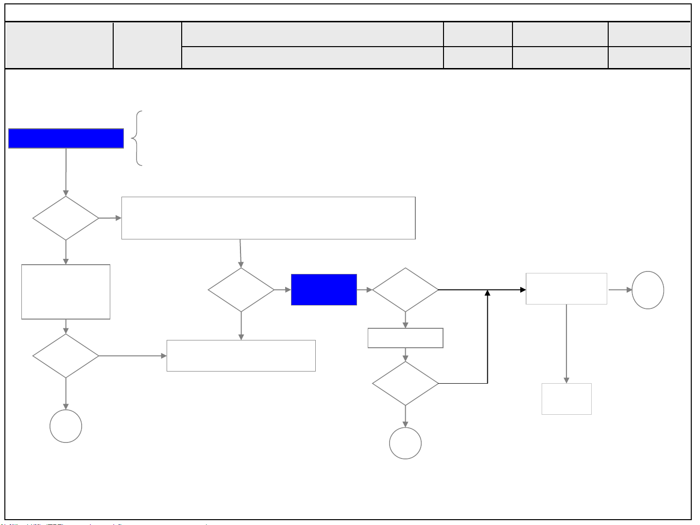
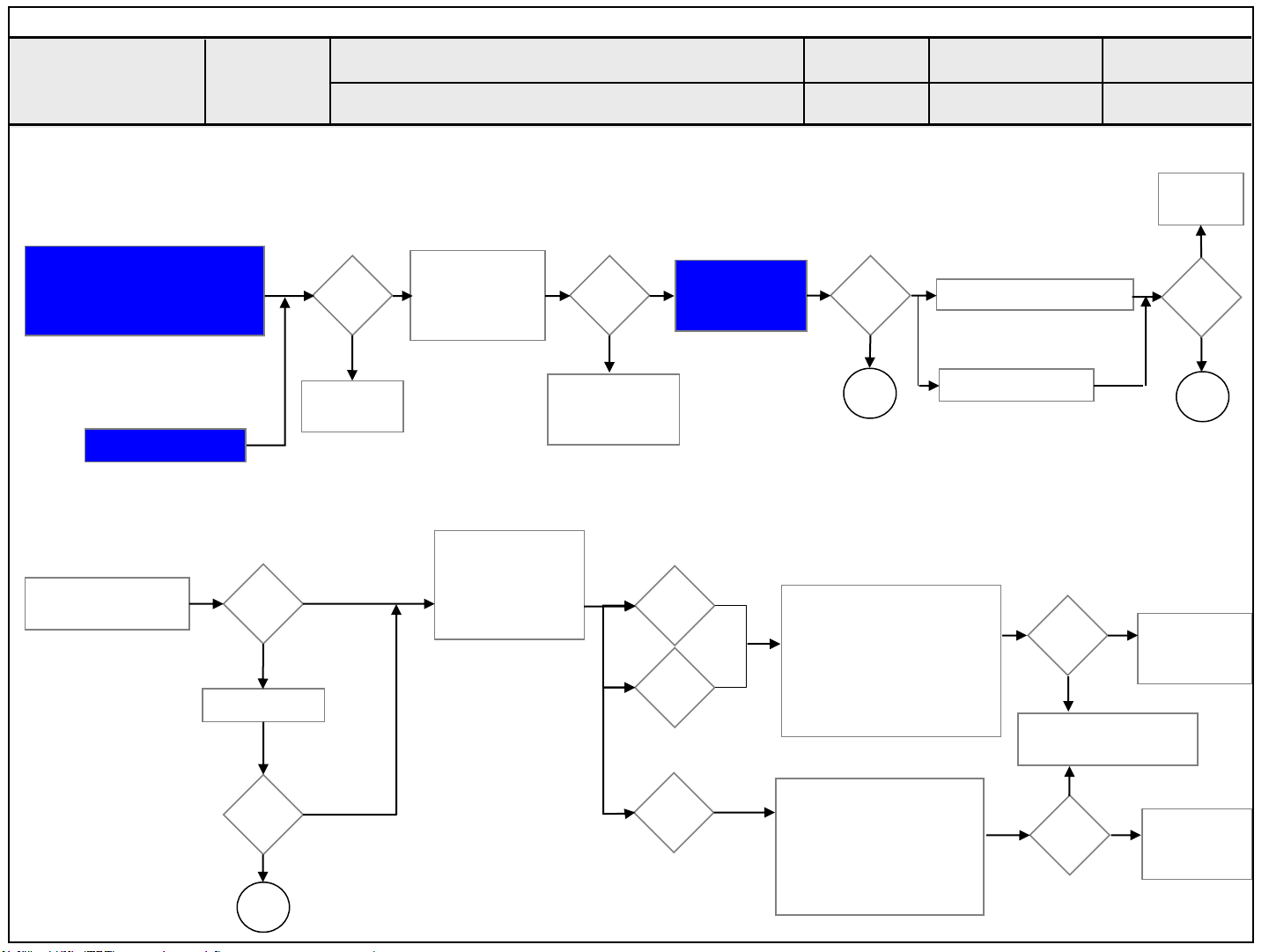
Standard Repair Process
☞ A3
Check RF Signal level
Normal
Signal?
N
Check RF Cable
Connection
1. Reconnection
2. Install Booster
Normal
Picture?
Y
Close
Y
N
Error
symptom
A. Video error
Picture broken/ Freezing
Established
date
Revised date
. By using Digital signal level meter
. By using Diagnostics menu on OSD
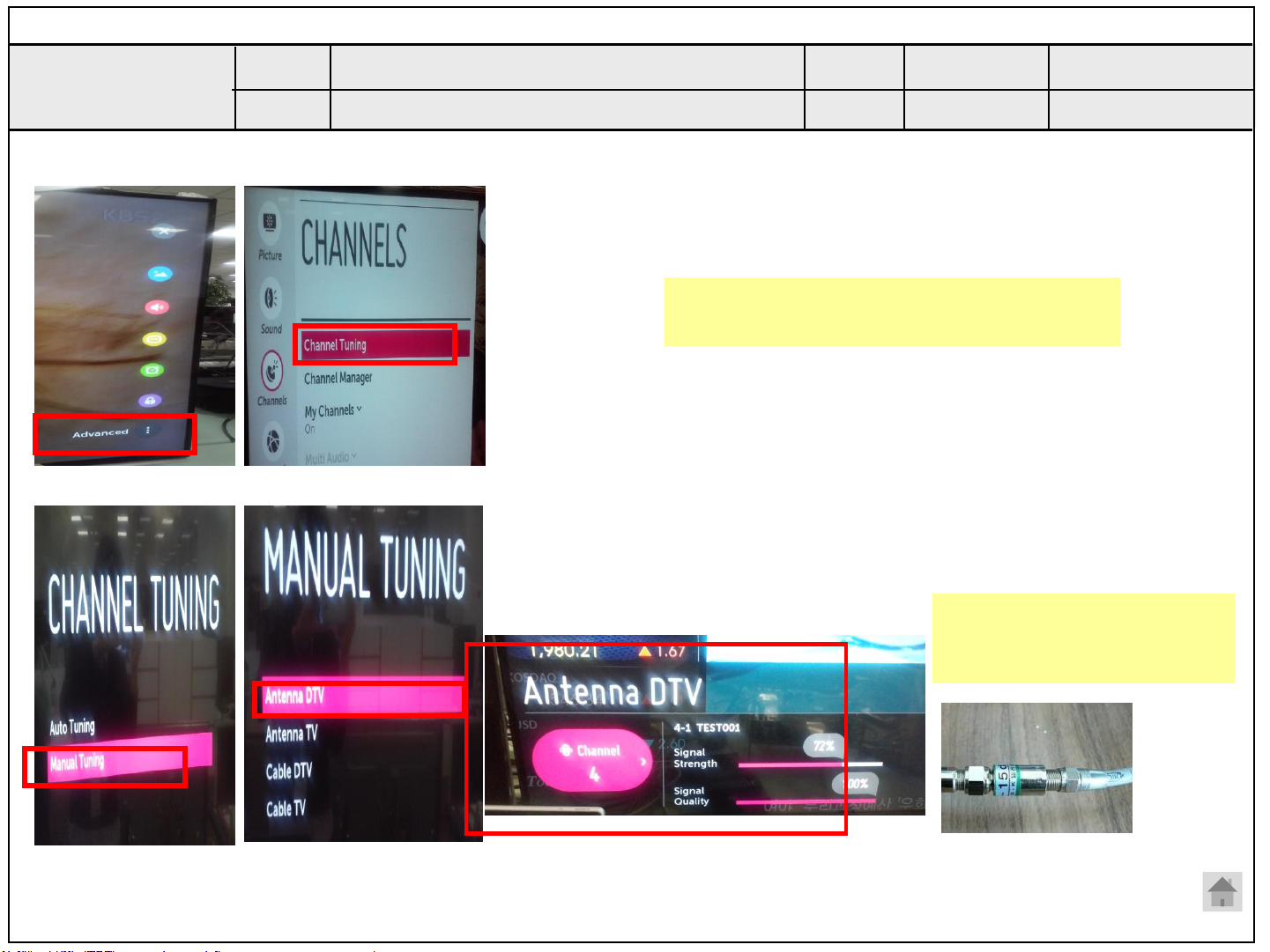
( Advanced→ Channels→ Channel Tuning→ Manual Tuning → Check the Signal )
- Signal strength (Normal : over 50%)
- Signal Quality (Normal: over 50%)
Check whether other equipments have problem or not.
(By connecting RF Cable at other equipment)
→ DVD Player ,Set-Top-Box, Different maker TV etc`
☞ A4
Normal
Picture?
Contact with signal distributor
or broadcaster (Cable or Air)
Y
S/W Version
N
Check
SVC
Bulletin?
S/W Upgrade
Normal
Picture?
Y
N
Y
N
Check
Tuner soldering
N
Replace
Main B/D
Y
3/16
Close
3
Close
Page 30
Standard Repair Process
☞A6
Check color by input
-External Input
-COMPONENT
-AV
-HDMI
☞A8
Check Test pattern
Error
symptom
Color
error?
Check error
color input
mode
☞ A7
※ Check
and replace
Y
Link Cable
(V by one)
N
and contact
condition
External Input/
Component
error
A. Video error
Color error
Color
error?
Check
external
device and
cable
N
Y
Replace Main B/D
Established
date
Revised date
External device
/Cable
normal
N
Color
error?
End
Y
4/16
Y
Replace module
N
Replace Main/T-con B/D
HDMI
error
Check external
device and
cable
4
Request repair
for external
device/cable
N
External device
/Cable
normal
Y
Replace Main/T-con B/D
Page 31
Standard Repair Process
symptom
Vertical / Horizontal bar, residual image,
Error
A. Video error
light spot, external device color error
Vertical/Horizontal bar, residual image, light spot
☞A6
Check color condition by input
-External Input
-Component
-HDMI
☞A8
Check Test pattern
Screen
normal?
N
Replace
module
Check external
Y
device
connection
condition
Normal?
N
Request repair
for external
device
External device screen error-Color error
Check screen
condition by input
Check S/W Version
Check
version
Y
S/W Upgrade
N
-External Input
-Component
-HDMI/DVI
Component
☞ A7
Check and
Y
replace Link
Cable
External
Input
error
error
Established
date
Revised date
Y
N
Replace Main/T-con B/D
For LGD panel
Replace Main B/D
Screen
normal?
End
For other panel
Connect other external
device and cable
(Check normal operation of
External Input, Component,
RGB and HDMI/DVI by
connecting Jig, pattern
Generator ,Set-top Box etc.
Screen
N
normal?
Y
Request repair for
external device
5/16
Replace
Module
N
Screen
normal?
Y
End
Replace
Main/T-con
B/D
Normal
screen?
Y
End
N
5
HDMI/
DVI
Connect other external
device and cable
(Check normal operation of
External Input, Component,
RGB and HDMI/DVI by
connecting Jig, pattern
Generator ,Set-top Box etc.
Y
Screen
normal?
N
Replace
Main /T-con
B/D
Page 32
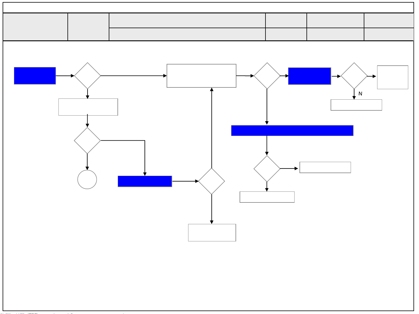
Standard Repair Process
symptom
☞A17
Check
Logo LED
. Stand-By: Red or Turn On
. Operating: Turn Off
Power LED
Check Power cord
was inserted properly
Error
On?
N
Normal?
Y
Close
Y
N
※
B. Power error
Check ST-BY 3.5V
☞A18
No power
DC Power on
by pressing Power Key
On Remote control
Y
Normal
Y
voltage?
N
Established
date
Revised date
☞A18
Y
N
Check Power
On ‘”High”
Replace Main B/D
Normal
operation?
☞A18
Measure voltage of each output of Power B/D
N
Y
Replace Main B/D
Normal
voltage?
Replace Power B/D
OK?
Y
6/16
Replace
Power
B/D
Replace Power
B/D
6
Page 33
Standard Repair Process
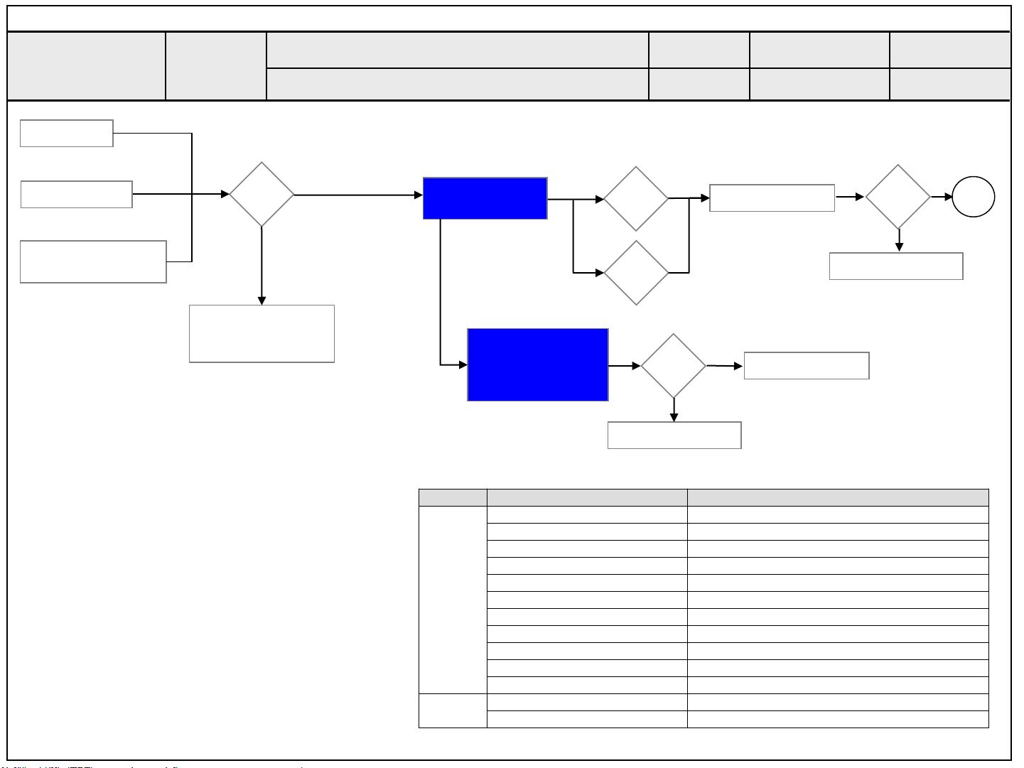
Check outlet
Check A/C cord
Check for all 3- phase
power out
Error
symptom
Error?
Y
Fix A/C cord & Outlet
and check each 3
phase out
B. Power error
Off when on, off while viewing, power auto on/off
☞A19
N
Check Power Off
Mode
☞A18
(If Power Off mode
is not displayed)
Check Power B/D
voltage
※ Caution
Check and fix exterior
of Power B/D Part
Abnormal
Abnormal
Established
date
Revised date
CPU
1
Normal
voltage?
Replace Power B/D
Replace Main B/D
Y
N
Replace Power B/D
Replace Main B/D
Normal?
N
7/16
Y
End
* Please refer to the all cases which
can be displayed on power off mode.
Status Power off List Explanation
"POWEROFF_REMOTEKEY" Power off by REMOTE CONTROL
"POWEROFF_OFFTIMER" Power off by OFF TIMER
"POWEROFF_SLEEPTIMER" Power off by SLEEP TIMER
"POWEROFF_INSTOP" Power off by INSTOP KEY
"POWEROFF_AUTOOFF" Power off by AUTO OFF
Normal
Abnormal
"POWEROFF_ONTIMER" Power off by ON TIMER
"POWEROFF_RS232C" Power off by RS232C
"POWEROFF_RESREC" Power off by Reservated Record
"POWEROFF_RECEND" Power off by End of Recording
"POWEROFF_SWDOWN" Power off by S/W Download
"POWEROFF_UNKNOWN" Power off by unknown status except listed case
"POWEROFF_ABNORMAL1" Power off by abnormal status except CPU trouble
"POWEROFF_CPUABNORMAL" Power off by CPU Abnormal
7
Page 34
Standard Repair Process
No audio
Screen normal
Error
C. Audio error
symptom
No audio/ Normal video
☞A20 ☞A21+A18
Check user
menu >
Speaker off
Off
Y
Cancel OFF
Check audio B+
N
13V of Power
Board
Established
date
Revised date
Normal
voltage
Replace Power Board and repair parts
Y
N
8/16
Check
Speaker
disconnection
Disconnection
Y
Replace Speaker
8
N
Replace MAIN Board
End
Page 35
Standard Repair Process
Check input
signal
-RF
-External Input
signal
Error
symptom
C. Audio error
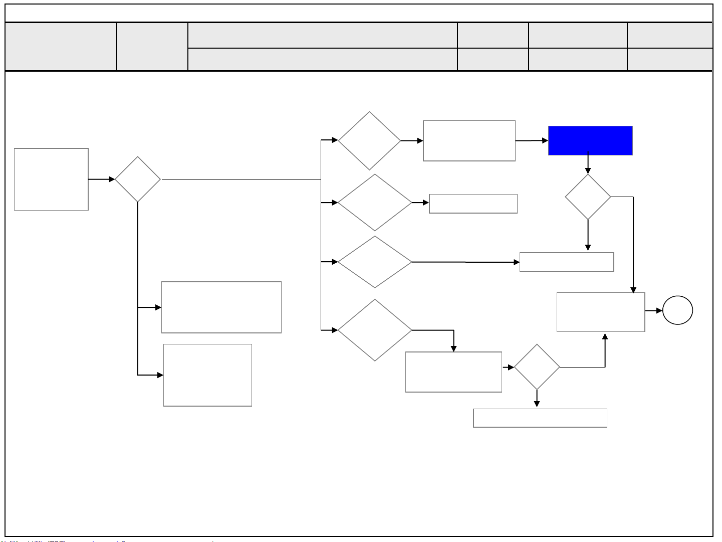
Wrecked audio/ discontinuation/noise
Established
date
Revised date
→ abnormal audio/discontinuation/noise is same after “Check input signal” compared to No audio
☞A21+A18
Check audio
B+ Voltage (13V)
Y
Normal
voltage?
N
Replace Power B/D
Replace Main B/D
N
Y
Signal
normal?
N
Y
(When RF signal is not
received)
Request repair to external
cable/ANT provider
(In case of
External Input
signal error)
Check and fix
external device
Wrecked audio/
Discontinuation/
Noise for
all audio
Wrecked audio/
Discontinuation/
Noise only
for D-TV
Wrecked audio/
Discontinuation/
Noise only
for Analog
Wrecked audio/
Discontinuation/
Noise only
for External Input
Check and replace
speaker and
connector
Replace Main B/D
Connect and check
other external
device
Normal
audio?
9/16
End
9
Check and fix external device
Page 36
Standard Repair Process
Error
symptom
D. Function error
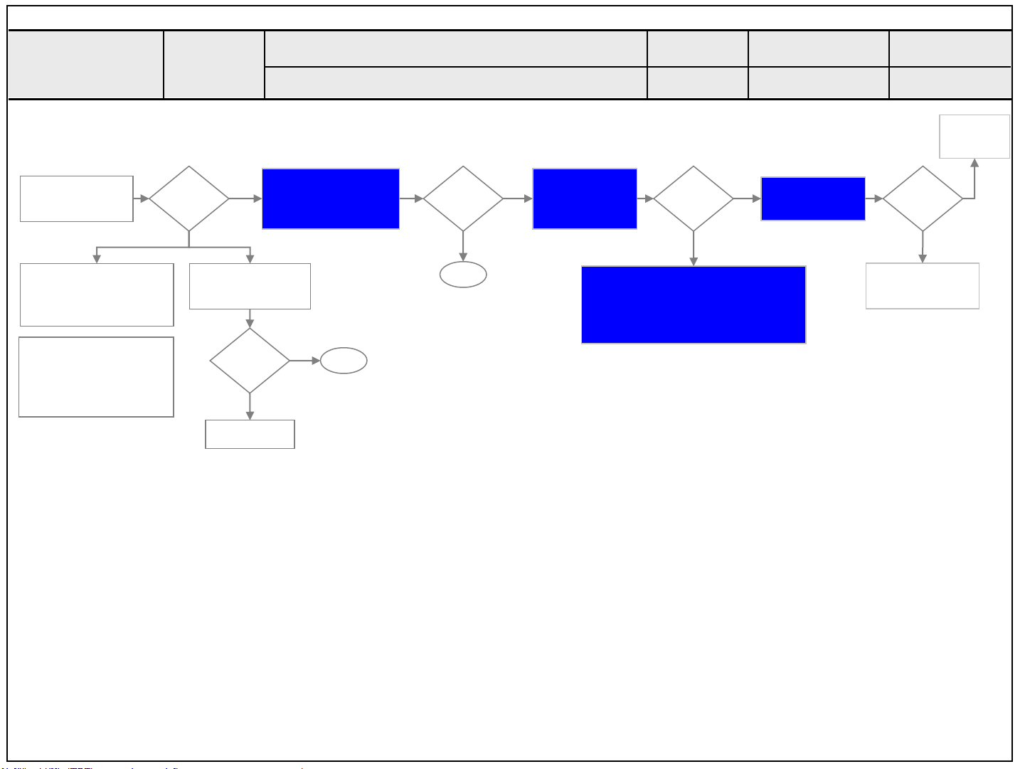
Remote control & Local switch checking
1. Remote control(R/C) operating error
☞A22
Check R/C itself
Operation
Check R/C Operating
When turn off light
in room
If R/C operate,
Explain the customer
cause is interference
from light in room.
operating?
Normal
Y
N
Check & Replace
Baterry of R/C
Normal
operating?
Replace R/C
Check & Repair
Cable connection
Connector solder
Y
Close
N
Normal
operating?
Y
Close
☞A22
N
Check B+
On Main B/D
Established
date
Revised date
Y
N
3.5V
Normal
Voltage?
☞A18
Check 3.5v on Power B/D
Replace Power B/D or
Replace Main B/D
(Power B/D don’t have problem)
☞A22
Check IR
Output signal
10/16
Replace
Main B/D
Normal
Signal?
N
Repair/Replace
IR B/D
Y
10
Page 37
Standard Repair Process
Error
symptom
D. Function error
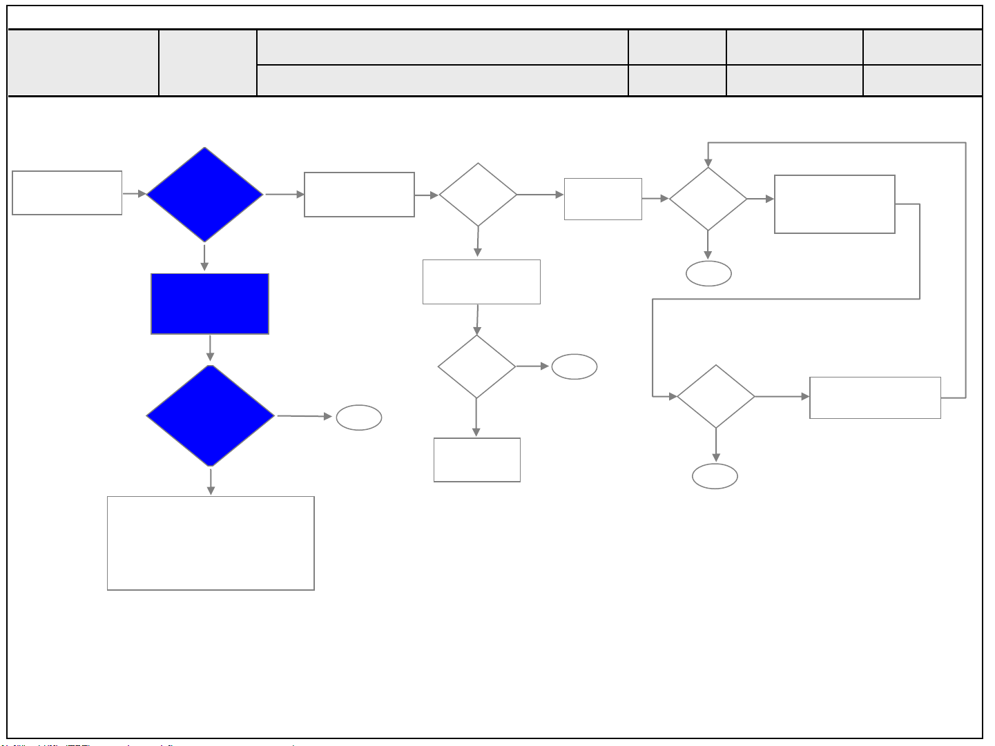
2. MR15 (Magic Remocon) operating error
☞A4
Check the
INSTART menu
RF Receiver ver
is “00.00”?
☞A23
Check & Repair
connection
Y
RF assy
☞A4
RF Receiver ver
is “00.00”?
Y
N
Check MR15
itself Operation
N
Close
MR15 operating checking
Normal
operating?
Check & Replace
Battery of MR15
Normal
operating?
N
Replace
MR15
Y
N
Y
Press the
wheel
Close
Established
date
Revised date
Is show ok
message?
Y
Close
Is show ok
message?
Close
Y
Turn off/on the
N
set and press
the wheel
N
11/16
Press the back
key about 5sec
Down load the Firmware
* INSTART MENU14.RF
Remocon Test3. Firmware
download
• If you conduct the loop at 3times,
change the MR15
11
Page 38
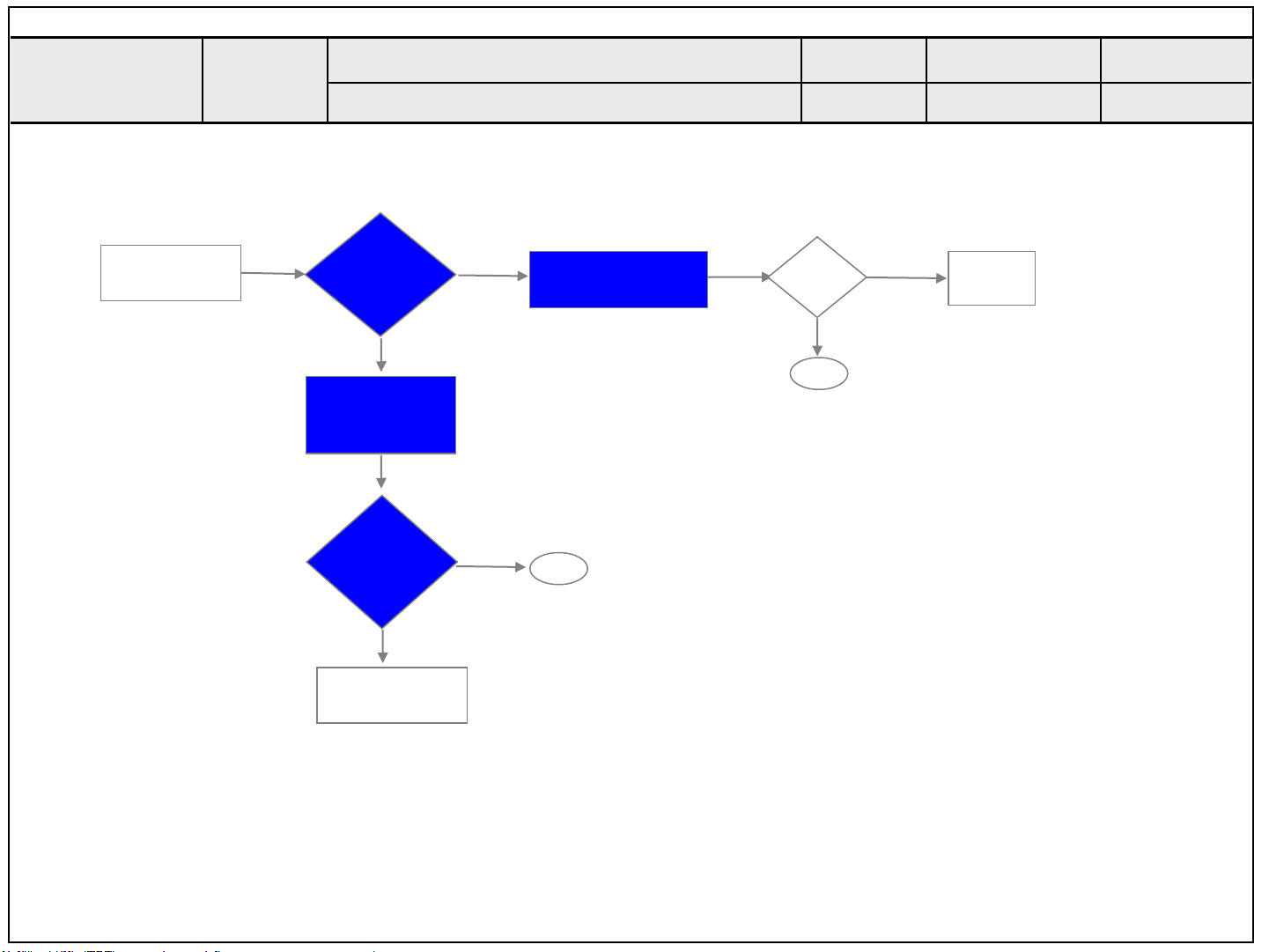
Standard Repair Process
Error
symptom
3.Wifi operating error
☞A4
Check the
INSTART menu
Wi-Fi Mac value
is “NG”?
☞A24
Check & Repair
connection
Y
Wifi cable
☞A4
Wi-Fi Mac value
is “NG”?
D. Function error
Wifi operating checking
☞A24
N
Check the Wifi wafer
N
Close
1pin
Established
Revised date
Normal
Voltage?
Y
Close
date
N
12/16
Replace
Main B/D
Y
Change the Wifi
assy
12
Page 39
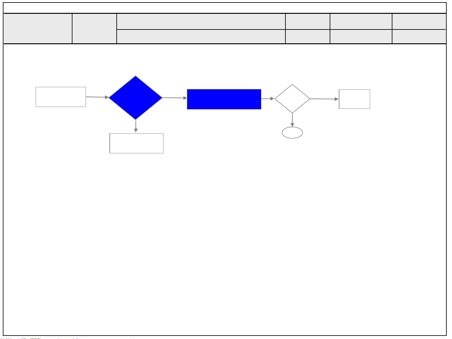
Standard Repair Process
Error
symptom
4.Camera operating error
☞A4
Check the
INSTART menu
Camera module
D. Function error
Camera Ver.
is “NULL”?
Y
Change the
Camera operating checking
☞A25
N
Reconnect the
Camera module
Established
date
Revised date
Normal
operation?
Y
Close
N
13/16
Replace
Main B/D
13
Page 40
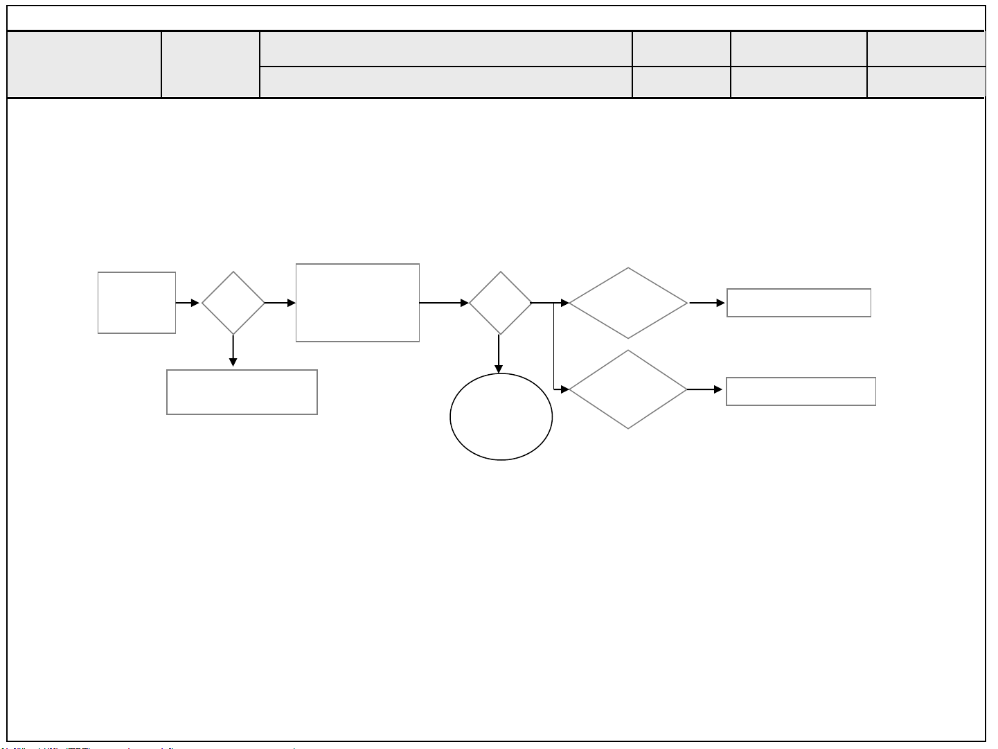
Standard Repair Process
Check
input
signal
symptom
Signal
input?
N
Y
Check technical
information
- Fix information
- S/W Version
Check and fix
external device/cable
Error
D. Function error
External device recognition error
Technical
information?
Y
Fix in
accordance
with technical
information
External Input and
N
Component
Recognition error
DVI, Optical
Recognition error
Established
Revised date
HDMI/
date
14/16
Replace Main B/D
Replace Main B/D
14
Page 41
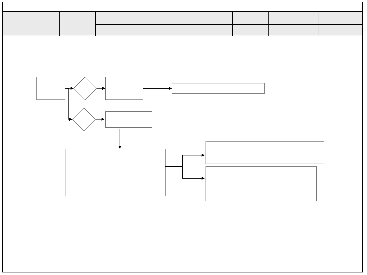
Standard Repair Process
Identify
nose
type
Error
symptom
Circuit
noise
Mechanical
noise
※ Mechanical noise is a natural
phenomenon, and apply the 1st level
description. When the customer does not
agree, apply the process by stage.
※ Describe the basis of the description
in “Part related to nose” in the Owner’s
Manual.
Circuit noise, mechanical noise
Check
location of
noise
Check location of
noise
E. Noise
Replace PSU
※ When the nose is severe, replace the module
(For models with fix information, upgrade the
S/W or provide the description)
OR
※ If there is a “Tak Tak” noise from the
cabinet, refer to the KMS fix information and
then proceed as shown in the solution manual
(For models without any fix information,
provide the description)
Established
date
Revised date
15/16
15
Page 42
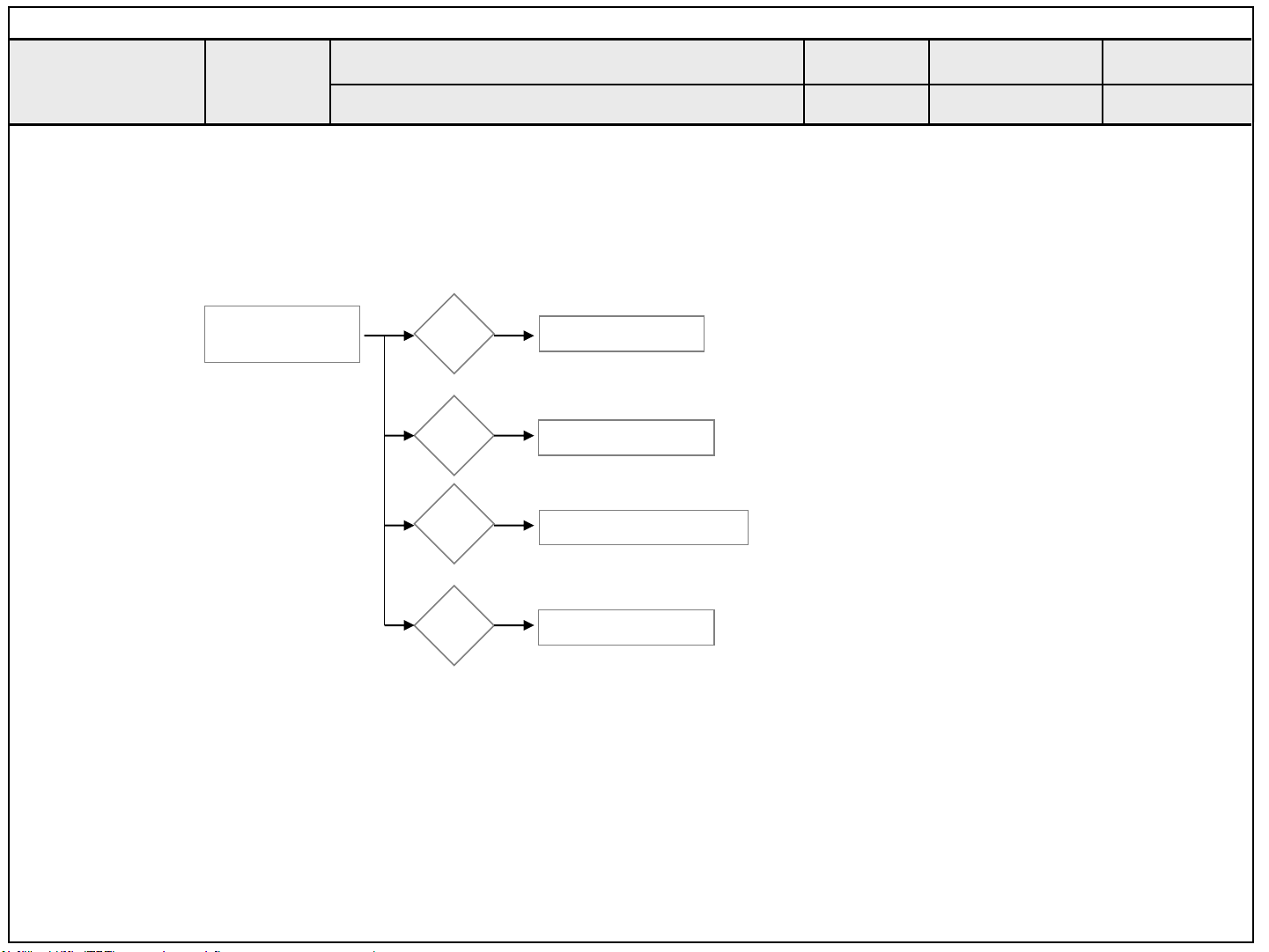
Standard Repair Process
Error
symptom
Zoom part with
exterior damage
Module
damage
Cabinet
damage
Remote
control
damage
F. Exterior defect
Exterior defect
Replace module
Replace cabinet
Replace remote control
Established
date
Revised date
16/16
Stand
dent
Replace stand
16
Page 43
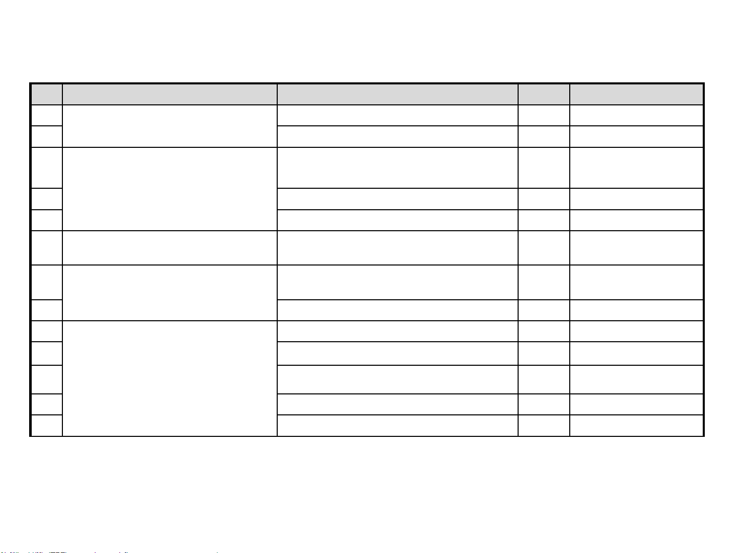
Contents of Standard Repair Process Detail Technical Manual
No. Error symptom Content Page Remarks
1
A. Video error_ No video/Normal
audio
2 Check White Balance value A2
3
A. Video error_ video error /Video
lag/stop
4 Version checking method A4
5 Tuner Checking Part A5
A. Video error _Vertical/Horizontal bar,
6
residual image, light spot
7
A. Video error_ Color error
8 Adjustment Test pattern - ADJ Key A8
9
10 Exchange Main Board (2) A-2/5
<Appendix>
11 Exchange Power Board (PSU) A-3/5
Defected Type caused by T-Con/
Inverter/ Module
12 Exchange Module (1) A-4/5
Check LCD back light with naked eye A1
TUNER input signal strength checking
method
Connection diagram A6
Check Link Cable (EPI) reconnection
condition
Exchange Main Board (1) A-1/5
A3
A7
13 Exchange Module (2) A-5/5
Continue to the next page
Page 44
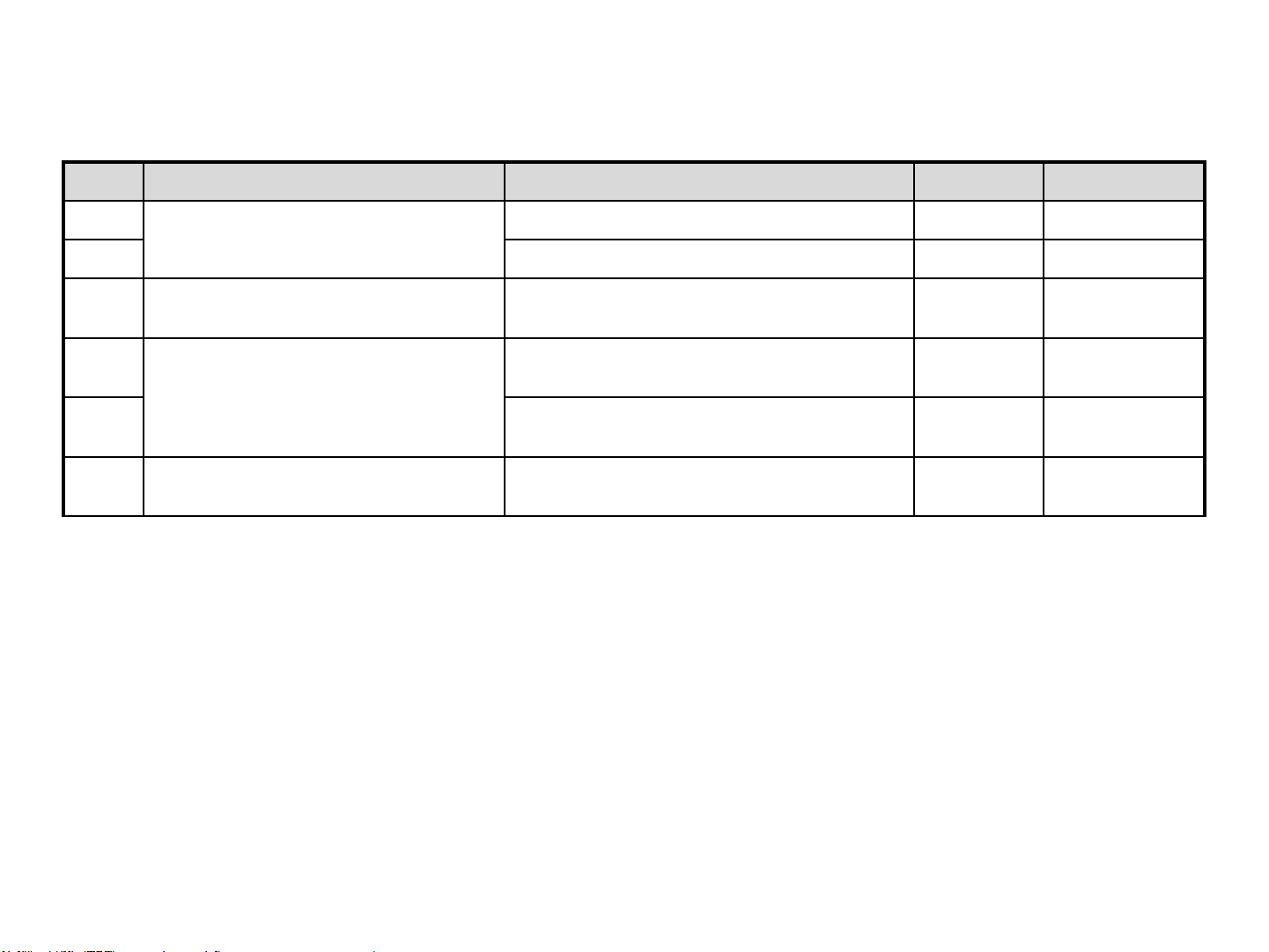
Contents of Standard Repair Process Detail Technical Manual
Continued from previous page
No. Error symptom Content Page Remarks
14
B. Power error_ No power
15 Check power input Voltage & ST-BY 3.5V A18
16
17
18
19 D. Function error
B. Power error_Off when on, off
while viewing
C. Audio error_ No audio/Normal
video
Check front display LED A17
POWER OFF MODE checking method A19
Checking method in menu when there is
no audio
Voltage and speaker checking method
when there is no audio
Remote control operation checking
method
A20
A21
A22
Page 45
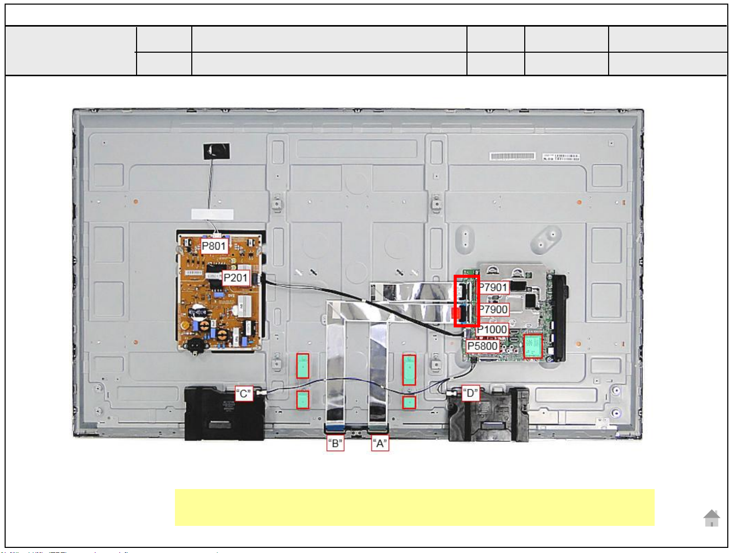
Standard Repair Process Detail Technical Manual
<ALL MODELS>
Error
symptom
Content
A. Video error_No video/Normal audio
Check LCD back light with naked eye
Established
date
Revised
date
A1
After turning on the power and disassembling the case, check with the naked eye,
whether you can see light from locations.
A1
Page 46
Standard Repair Process Detail Technical Manual
Error
symptom
Content
<ALL MODELS>
A. Video error_No video/Normal audio
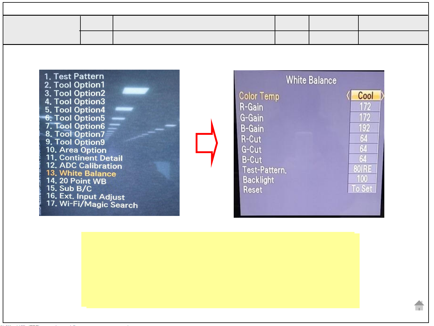
Check White Balance value
Established
date
Revised
date
A2
Entry method
Entry method
1. Press the ADJ button on the remote controller for adjustment.
1. Press the ADJ button on the remote controller for adjustment.
2. Enter into White Balance of item 6.
2. Enter into White Balance of item 13.
3. After recording the R, G, B (GAIN, Cut) value of Color Temp
3. After recording the R, G, B (GAIN, Cut) value of Color Temp
(Cool/Medium/Warm), re-enter the value after replacing the MAIN BOARD.
(Cool/Medium/Warm), re-enter the value after replacing the MAIN BOARD.
A2
Page 47
Standard Repair Process Detail Technical Manual
<ALL MODELS>
Error
symptom
Content
A. Video error_Video error, video lag/stop
TUNER input signal strength checking method
Established
date
Revised
date
Advanced Channels Channel Tuning
Manual Tuning
A3
A3
When the signal is strong,
use the attenuator (-10dB, -
15dB, -20dB etc.)
Page 48
Standard Repair Process Detail Technical Manual
Error
symptom
Content
A. Video error_Video error, video lag/stop
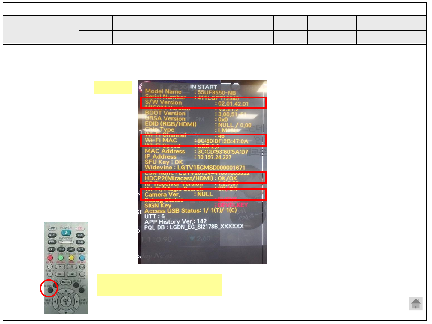
Version checking method
Established
date
Revised
date
A4
<ALL MODELS>
1. Checking method for remote control for adjustment
Version
v
v
Press the IN-START with the remote
control for adjustment
A4
Page 49
Standard Repair Process Detail Technical Manual
<ALL MODELS>
Error
symptom
Content
A. Video error_Video error, video lag/stop
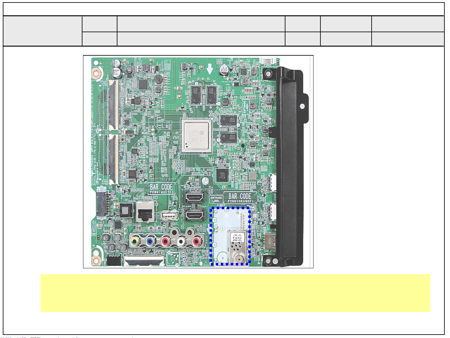
TUNER checking part
Established
date
Revised
date
A5
Checking method:
1. Check the signal strength or check whether the screen is normal when the external device is connected.
2. After measuring each voltage from power supply, finally replace the MAIN BOARD.
3. If you can`t see the UHD live TV, please connect signal at left side of jack. (Korea model only)
A5
Page 50
Standard Repair Process Detail Technical Manual
<ALL MODELS>
Error
symptom
Content
A. Video error _Vertical/Horizontal bar,
residual image, light spot
Connection diagram (1)
Established
date
Revised
date
A6
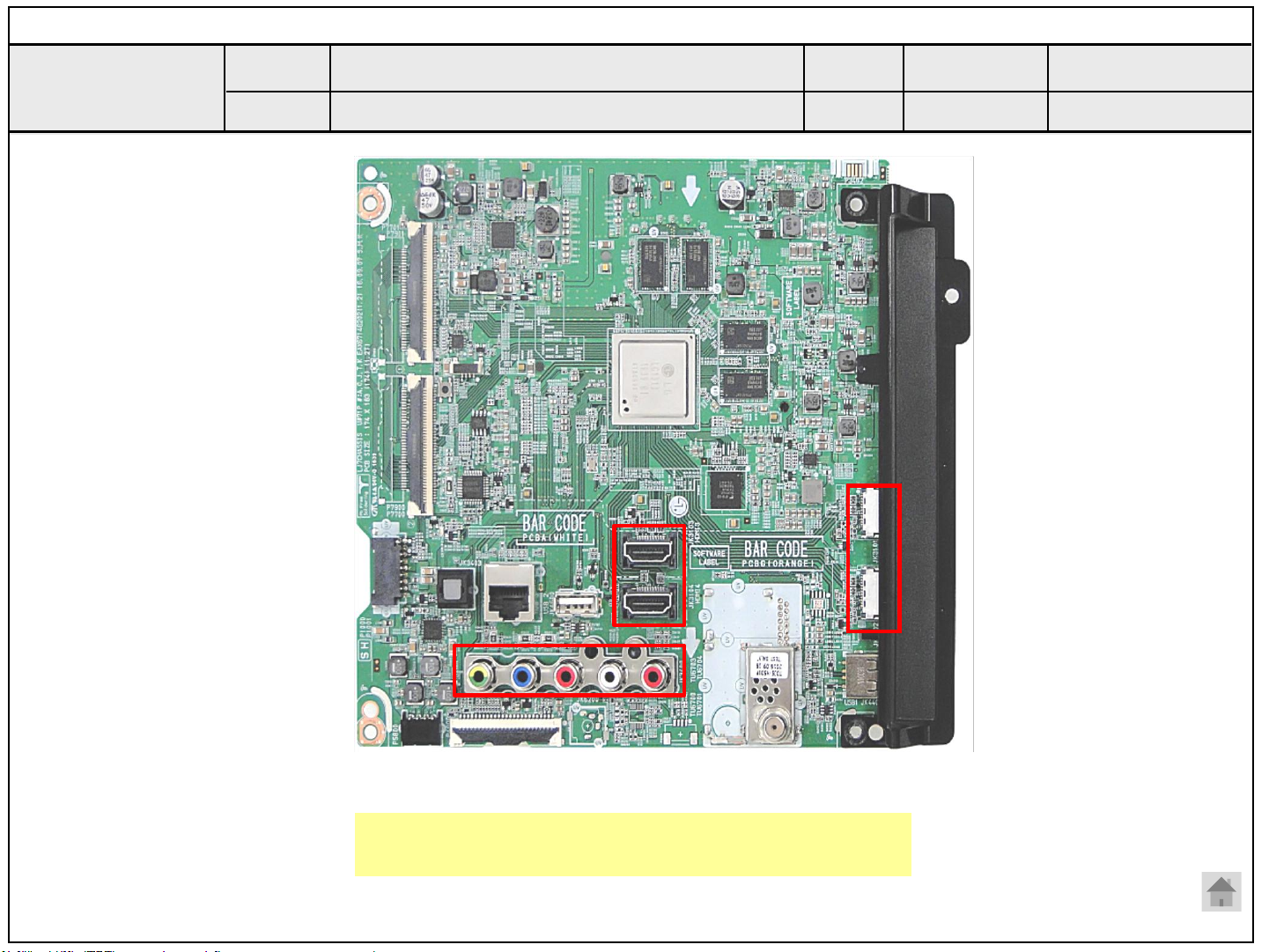
As the part connecting to the external input, check
the screen condition by signal
A6
Page 51
Standard Repair Process Detail Technical Manual
<ALL MODELS>
Error
symptom
Content
Check Link Cable(FFC) reconnection condition
A. Video error_Color error
Established
date
Revised
date
A7
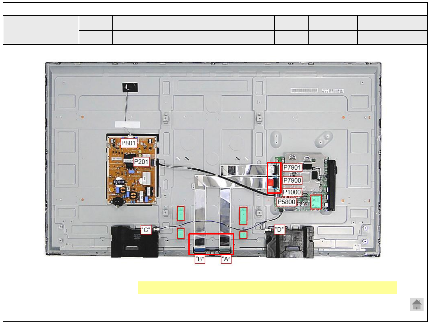
Check the contact condition of the Link Cable, especially dust or mis insertion.
A7
Page 52
Standard Repair Process Detail Technical Manual
Error
symptom
Content
A. Video error_Color error
Adjustment Test pattern - ADJ Key
Established
date
Revised
date
A8
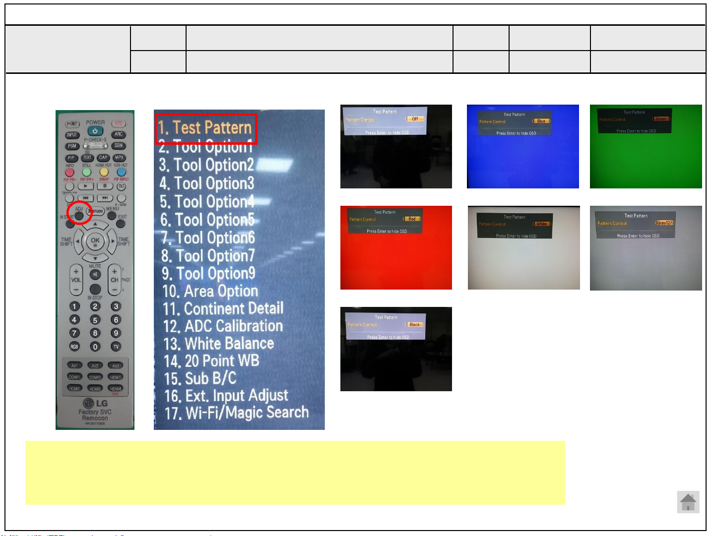
You can view 6 types of patterns using the ADJ Key
Checking item : 1. Defective pixel 2. Residual image 3. MODULE error (ADD-BAR,SCAN BAR..)
4.Video error (Classification of MODULE or Main-B/D!)
A8
Page 53
Appendix : Exchange Main Board (1)
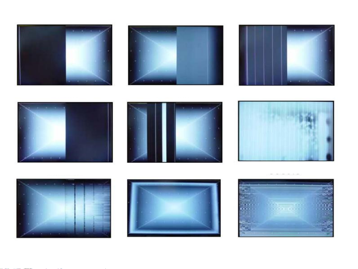
Solder defect, CNT Broken
Solder defect, CNT Broken
Solder defect, CNT Broken
T-Con Defect, CNT Broken
T-Con Defect, CNT Broken
Solder defect, CNT Broken
T-Con Defect, CNT Broken
Solder defect, CNT Broken
Abnormal Power Section
Solder defect, Short/Crack
Abnormal Power Section Solder defect, Short/Crack
A - 1/5
Page 54
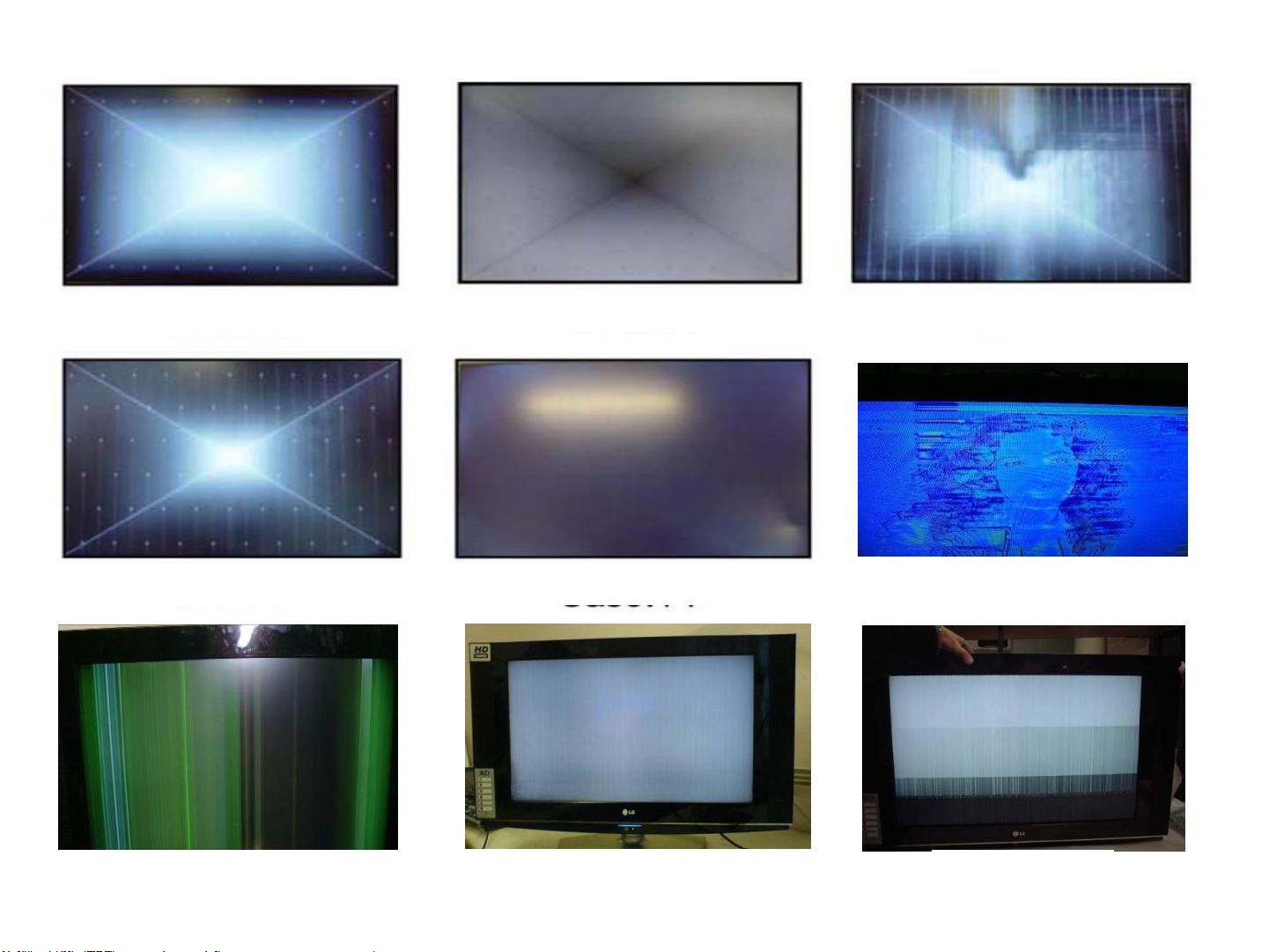
Appendix : Exchange Main Board (2)
Abnormal Power Section
Solder defect, Short/Crack
Abnormal Power Section
Fuse Open, Abnormal power section
Solder defect, Short/Crack
Abnormal Display
GRADATION
Noise
A - 2/5
GRADATION
Page 55
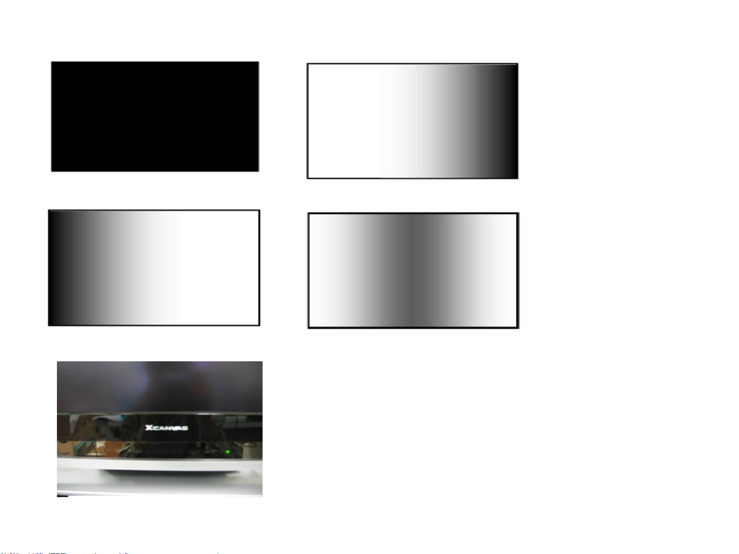
Appendix : Exchange Power Board (PSU)
No Light
Dim Light
Dim Light
Dim Light
No picture/Sound Ok
A - 3/5
Page 56
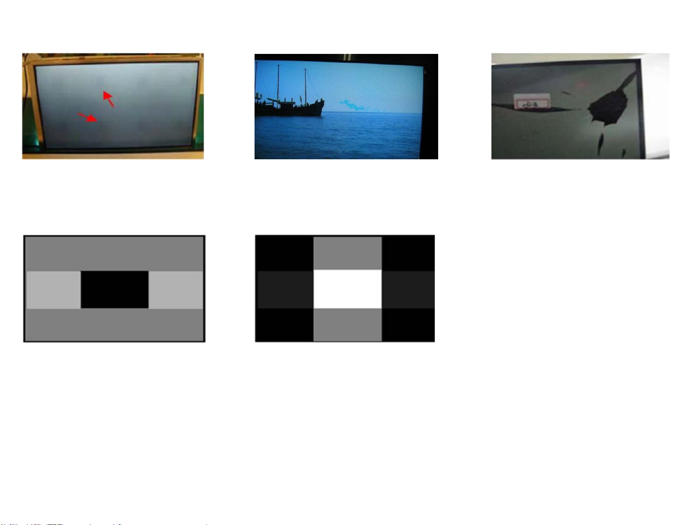
Appendix : Exchange the Module (1)
Press damage Press damage
Crosstalk Crosstalk
Press damage
Un-repairable Cases
In this case please exchange the module.
A - 4/5
Page 57
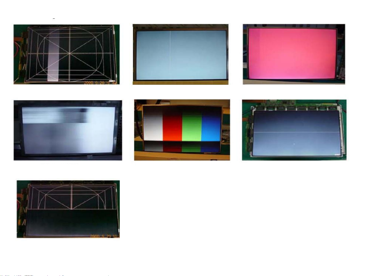
Appendix : Exchange the Module (2)
Vertical Block
Source TAB IC Defect
Horizontal Block
Gate TAB IC Defect
Vertical Line
Source TAB IC Defect
Horizontal Block
Gate TAB IC Defect
Gate TAB IC Defect
Vertical Block
Source TAB IC Defect
Horizontal line
Gate TAB IC Defect
Gate TAB IC Defect
Un-repairable Cases
In this case please exchange the module.
Horizontal Block
Gate TAB IC Defect
Gate TAB IC Defect
A - 5/5
Page 58
Standard Repair Process Detail Technical Manual
<ALL MODELS>
Error
symptom
Content
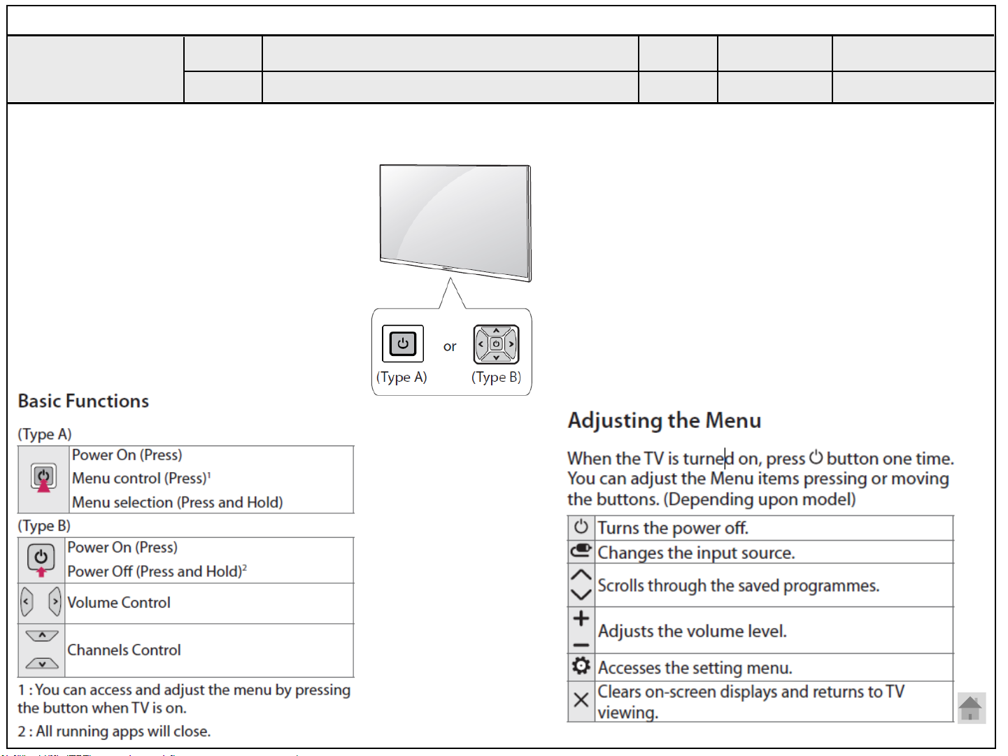
B. Power error _No power
Check front Power Indicator
Established
date
Revised
date
A17
A17
Page 59
Standard Repair Process Detail Technical Manual
Backlight
Forward
Voltage
Symbol
Values
Unit
Min
Typ
Max
65UJ65
VF
117.18
130.2
143.22
Vdc
60UJ65
111.87
124.3
136.73
55UJ65
99.4
106.6
113.8
49UJ65
-
85.05
91.8
43UJ65
-
65.94
71.4
Backlight
Forward
Voltage
Symbol
Values
Unit
Min
Typ
Max
65UJ63
VF
-
192
216
Vdc
60UJ63
-
175
195
55UJ63
-
130.4
141.2
49UJ63
-
111.6
118.8
43UJ63
-
65.94
71.4
Error
symptom
Content
B. Power error _No power
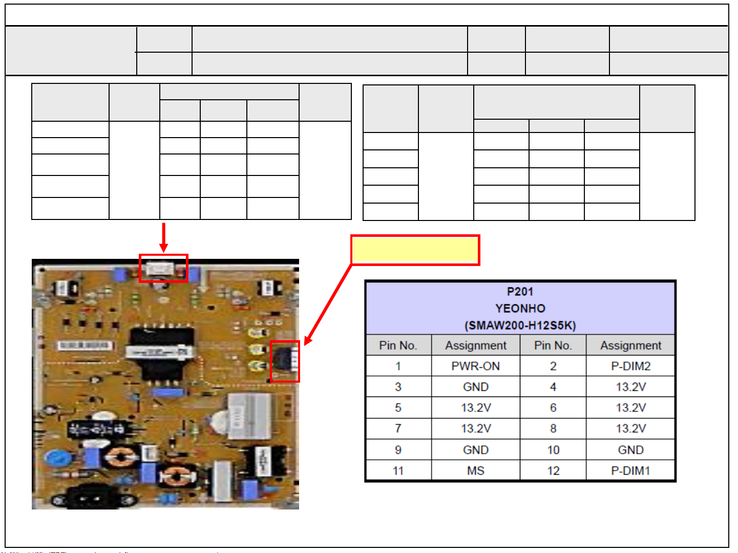
Check power input voltage and ST-BY 3.5V
Check the DC 13V
Established
date
Revised
date
A18
A18
Page 60
Standard Repair Process Detail Technical Manual
<ALL MODELS>
Error
symptom
Content
B. Power error _Off when on, off whiling viewing
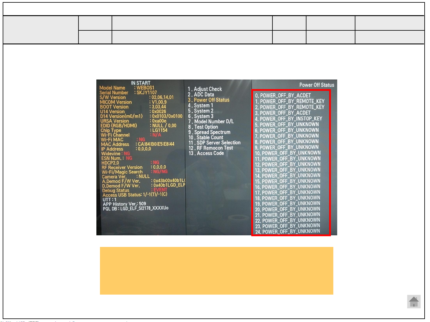
POWER OFF MODE checking method
Established
date
Revised
date
A19
Entry method
1. Press the IN-START button of the remote control for adjustment
2. Check the entry into adjustment item 3
A19
Page 61
Standard Repair Process Detail Technical Manual
<ALL MODELS>
Error
symptom
Content
C. Audio error_No audio/Normal video
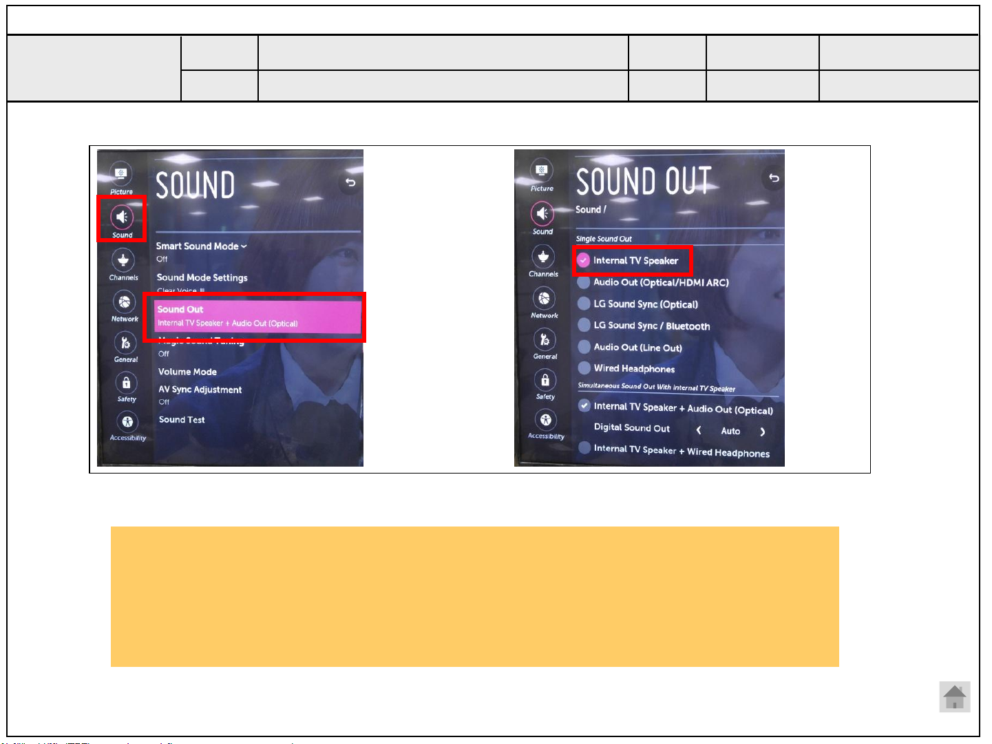
Checking method in menu when there is no audio
Established
date
Revised
date
A20
Checking method
1. Press the Setting button on the remote control
2. Select the Sound function of the Menu
3. Select the Sound Out
4. Select TV Speaker
A20
Page 62
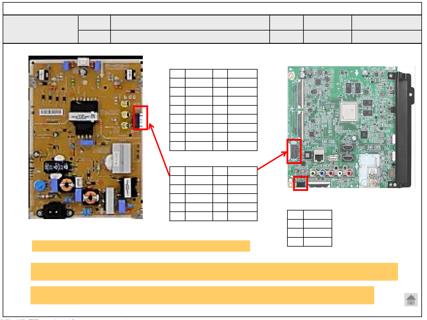
Standard Repair Process Detail Technical Manual
<ALL MODELS>
Checking order when there is no audio
1.Check the contact condition of or 13V connector of Main Board
Error
symptom
Content
C. Audio error_No audio/Normal video
Voltage and speaker checking method
when there is no audio
UJ7*
1 VSYNC 2 SIN
3 GND 4 SCLK
5 DRV_ON 6 PDIM1
7 GND 8 GND
9 A13 10 A13
11 D13 12 D13
13 GND 14 D13
②
15 PWR_ON 16 PDIM2
17 GND 18 GND
UJ6*
1 DRV_ON 2 PDIM1
3 GND 4 GND
5 A13 6 A13
7 D13 8 D13
9 GND 10 D13
11 PWR_ON 12 PDIM2
Established
date
Revised
date
①
③
1 SPK_R-
2 SPK_R+
3 SPK_L-
4 SPK_L+
A21
2. Measure the 13V input voltage supplied from Power Board
(If there is no input voltage, remove and check the connector)
3.Connect the tester RX1 to the speaker terminal and if you hear the Chik Chik sound when you touch the
GND and output terminal, the speaker is normal.
A21
Page 63
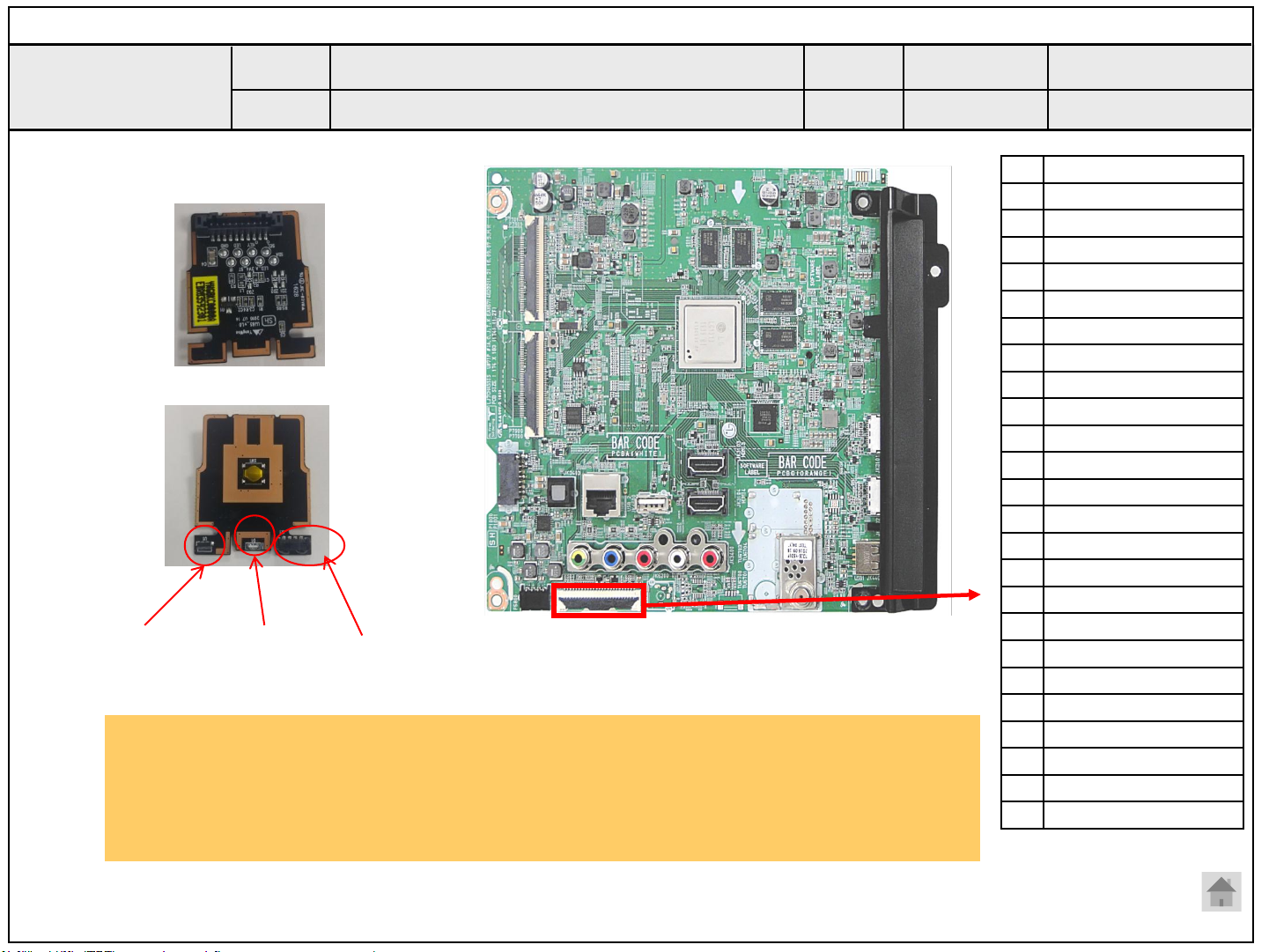
Standard Repair Process Detail Technical Manual
Error
symptom
Content
Remote control operation checking method
D. Function error
Established
date
Revised
date
A22
<ALL MODELS>
IR & LOGO light Front
IR & LOGO light Rear
Eye LED
Checking order to check remote control
Checking order
1.Check IR cable condition between IR & Main board.( Check picture number① and ②)
2.Check the standby 3.5V on the terminal 22 pin (③)
3.AS checking the Pre-Amp(IR LED light) , the power is in ON condition, an Analog Tester
needle should move slowly, otherwise, it’s defective.
IR
②
③
1 +3.5V
2 WIFI_DM
3 WIFI_DP
4 GND
5 WOL_ON
6 3.5V
7 COMBO_RESET
8 GND
9 COMBO_WAKEUP_DEVICE
10 COMBO_WAKEUP_HOST
11 GND
12 GND
13 NC
14 NC
15 NC
16 EYE_SDA
17 EYE_SCL
18 GND
19 IR
20 LED
21 GND
22 3.5V
23 KEY2
24 KEY1
25 GND
A22
Page 64
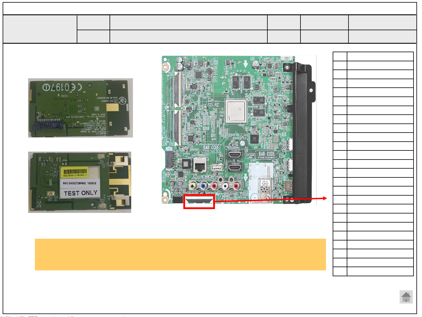
Standard Repair Process Detail Technical Manual
Error
symptom
Content
Remote control operation checking method
D. Function error
Established
date
Revised
date
A22
<ALL MODELS>
① Wifi & BT Front
Wifi & BT Rear
Checking order to check motion remote/wifi
Checking order
1.Check BT/Wifi cable condition between BT/Wifi assy & Main board.
2.Check the 3.5V on the terminal 1
②
③
1 +3.5V
2 WIFI_DM
3 WIFI_DP
4 GND
5 WOL_ON
6 3.5V
7 COMBO_RESET
8 GND
9 COMBO_WAKEUP_DEVICE
10 COMBO_WAKEUP_HOST
11 GND
12 GND
13 NC
14 NC
15 NC
16 EYE_SDA
17 EYE_SCL
18 GND
19 IR
20 LED
21 GND
22 3.5V
23 KEY2
24 KEY1
25 GND
A22
Page 65

 Loading...