

LG 32LH550B, 43LH570 SERIES, 43LH570-U, 49LH570 SERIES, 49LH570-U Service Manual
Printed in KoreaP/NO : MFL69442201 (1601-REV00)
CHASSIS : LA66K
MODEL : 32LH550B
CAUTION
BEFORE SERVICING THE CHASSIS,
READ THE SAFETY PRECAUTIONS IN THIS MANUAL.
LED TV
SERVICE MANUAL
Internal Use Only

- 2 -
LGE Internal Use OnlyCopyright © LG Electronics. Inc. All rights reserved.
Only for training and service purposes
CONTENTS
CONTENTS .............................................................................................. 2
SAFETY PRECAUTIONS ........................................................................ 3
SERVICING PRECAUTIONS ................................................................... 4
SPECIFICATION ....................................................................................... 6
ADJUSTMENT INSTRUCTION ................................................................ 9
BLOCK DIAGRAM ...................................................................................17
EXPLODED VIEW .................................................................................. 18
PRODUCT DISASSEMBLY PROCESS ...................................................19
SCHEMATIC CIRCUIT DIAGRAM ........................................... APPENDIX
TROUBLESHOOTING .............................................................. APPENDIX
- 3 -
LGE Internal Use Only
Copyright © LG Electronics. Inc. All rights reserved.
Only for training and service purposes
Many electrical and mechanical parts in this chassis have special safety-related characteristics. These parts are identified by in the
Schematic Diagram and Exploded View.
It is essential that these special safety parts should be replaced with the same components as recommended in this manual to prevent
Shock, Fire, or other Hazards.
Do not modify the original design without permission of manufacturer.
General Guidance
An isolation Transformer should always be used during the
servicing of a receiver whose chassis is not isolated from the AC
power line. Use a transformer of adequate power rating as this
protects the technician from accidents resulting in personal injury
from electrical shocks.
It will also protect the receiver and it's components from being
damaged by accidental shorts of the circuitry that may be
inadvertently introduced during the service operation.
If any fuse (or Fusible Resistor) in this TV receiver is blown,
replace it with the specified.
When replacing a high wattage resistor (Oxide Metal Film Resistor,
over 1 W), keep the resistor 10 mm away from PCB.
Keep wires away from high voltage or high temperature parts.
Before returning the receiver to the customer,
always perform an AC leakage current check on the exposed
metallic parts of the cabinet, such as antennas, terminals, etc., to
be sure the set is safe to operate without damage of electrical
shock.
Leakage Current Cold Check(Antenna Cold Check)
With the instrument AC plug removed from AC source, connect an
electrical jumper across the two AC plug prongs. Place the AC
switch in the on position, connect one lead of ohm-meter to the AC
plug prongs tied together and touch other ohm-meter lead in turn to
each exposed metallic parts such as antenna terminals, phone
jacks, etc.
If the exposed metallic part has a return path to the chassis, the
measured resistance should be between 1 MΩ and 5.2 MΩ.
When the exposed metal has no return path to the chassis the
reading must be infinite.
An other abnormality exists that must be corrected before the
receiver is returned to the customer.
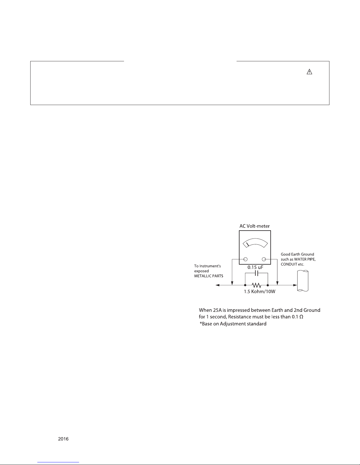
Leakage Current Hot Check (See below Figure)
Plug the AC cord directly into the AC outlet.
Do not use a line Isolation Transformer during this check.
Connect 1.5 K / 10 watt resistor in parallel with a 0.15 uF capacitor
between a known good earth ground (Water Pipe, Conduit, etc.)
and the exposed metallic parts.
Measure the AC voltage across the resistor using AC voltmeter
with 1000 ohms/volt or more sensitivity.
Reverse plug the AC cord into the AC outlet and repeat AC voltage
measurements for each exposed metallic part. Any voltage
measured must not exceed 0.75 volt RMS which is corresponds to
0.5 mA.
In case any measurement is out of the limits specified, there is
possibility of shock hazard and the set must be checked and
repaired before it is returned to the customer.
Leakage Current Hot Check circuit
IMPORTANT SAFETY NOTICE
SAFETY PRECAUTIONS

- 4 -
LGE Internal Use Only
Copyright © LG Electronics. Inc. All rights reserved.
Only for training and service purposes
SERVICING PRECAUTIONS
CAUTION: Before servicing receivers covered by this service
manual and its supplements and addenda, read and follow the
SAFETY PRECAUTIONS on page 3 of this publication.
NOTE: If unforeseen circumstances create conict between the
following servicing precautions and any of the safety precautions
on page 3 of this publication, always follow the safety precautions.
Remember: Safety First.
General Servicing Precautions
1. Always unplug the receiver AC power cord from the AC power
source before;
a. Removing or reinstalling any component, circuit board mod-
ule or any other receiver assembly.
b. Disconnecting or reconnecting any receiver electrical plug or
other electrical connection.
c. Connecting a test substitute in parallel with an electrolytic
capacitor in the receiver.
CAUTION: A wrong part substitution or incorrect polarity
installation of electrolytic capacitors may result in an explosion hazard.
2. Test high voltage only by measuring it with an appropriate
high voltage meter or other voltage measuring device (DVM,
FETVOM, etc) equipped with a suitable high voltage probe.
Do not test high voltage by "drawing an arc".
3. Do not spray chemicals on or near this receiver or any of its
assemblies.
4. Unless specied otherwise in this service manual, clean
electrical contacts only by applying the following mixture to the
contacts with a pipe cleaner, cotton-tipped stick or comparable
non-abrasive applicator; 10 % (by volume) Acetone and 90 %
(by volume) isopropyl alcohol (90 % - 99 % strength)
CAUTION: This is a ammable mixture.
Unless specied otherwise in this service manual, lubrication of
contacts in not required.
5. Do not defeat any plug/socket B+ voltage interlocks with which
receivers covered by this service manual might be equipped.
6. Do not apply AC power to this instrument and/or any of its
electrical assemblies unless all solid-state device heat sinks are
correctly installed.
7. Always connect the test receiver ground lead to the receiver
chassis ground before connecting the test receiver positive
lead.
Always remove the test receiver ground lead last.
8. Use with this receiver only the test xtures specied in this
service manual.
CAUTION: Do not connect the test xture ground strap to any
heat sink in this receiver.
Electrostatically Sensitive (ES) Devices
Some semiconductor (solid-state) devices can be damaged easily by static electricity. Such components commonly are called
Electrostatically Sensitive (ES) Devices. Examples of typical ES
devices are integrated circuits and some eld-effect transistors
and semiconductor “chip” components. The following techniques
should be used to help reduce the incidence of component damage caused by static by static electricity.
1. Immediately before handling any semiconductor component or
semiconductor-equipped assembly, drain off any electrostatic
charge on your body by touching a known earth ground. Alternatively, obtain and wear a commercially available discharging
wrist strap device, which should be removed to prevent potential shock reasons prior to applying power to the unit under test.
2. After removing an electrical assembly equipped with ES
devices, place the assembly on a conductive surface such as
aluminum foil, to prevent electrostatic charge buildup or exposure of the assembly.
3. Use only a grounded-tip soldering iron to solder or unsolder ES
devices.
4. Use only an anti-static type solder removal device. Some solder
removal devices not classied as “anti-static” can generate
electrical charges sufcient to damage ES devices.
5. Do not use freon-propelled chemicals. These can generate
electrical charges sufcient to damage ES devices.
6. Do not remove a replacement ES device from its protective
package until immediately before you are ready to install it.
(Most replacement ES devices are packaged with leads electrically shorted together by conductive foam, aluminum foil or
comparable conductive material).
7. Immediately before removing the protective material from the
leads of a replacement ES device, touch the protective material
to the chassis or circuit assembly into which the device will be
installed.
CAUTION: Be sure no power is applied to the chassis or circuit,
and observe all other safety precautions.
8. Minimize bodily motions when handling unpackaged replacement ES devices. (Otherwise harmless motion such as the
brushing together of your clothes fabric or the lifting of your
foot from a carpeted oor can generate static electricity sufcient to damage an ES device.)
General Soldering Guidelines
1. Use a grounded-tip, low-wattage soldering iron and appropriate
tip size and shape that will maintain tip temperature within the
range or 500 °F to 600 °F.
2. Use an appropriate gauge of RMA resin-core solder composed
of 60 parts tin/40 parts lead.
3. Keep the soldering iron tip clean and well tinned.
4. Thoroughly clean the surfaces to be soldered. Use a mall wirebristle (0.5 inch, or 1.25 cm) brush with a metal handle.
Do not use freon-propelled spray-on cleaners.
5. Use the following unsoldering technique
a. Allow the soldering iron tip to reach normal temperature.
(500 °F to 600 °F)
b. Heat the component lead until the solder melts.
c. Quickly draw the melted solder with an anti-static, suction-
type solder removal device or with solder braid.
CAUTION: Work quickly to avoid overheating the circuit
board printed foil.
6. Use the following soldering technique.
a. Allow the soldering iron tip to reach a normal temperature
(500 °F to 600 °F)
b. First, hold the soldering iron tip and solder the strand against
the component lead until the solder melts.
c. Quickly move the soldering iron tip to the junction of the
component lead and the printed circuit foil, and hold it there
only until the solder ows onto and around both the component lead and the foil.
CAUTION: Work quickly to avoid overheating the circuit
board printed foil.
d. Closely inspect the solder area and remove any excess or
splashed solder with a small wire-bristle brush.

- 5 -
LGE Internal Use Only
Copyright © LG Electronics. Inc. All rights reserved.
Only for training and service purposes
IC Remove/Replacement
Some chassis circuit boards have slotted holes (oblong) through
which the IC leads are inserted and then bent at against the circuit foil. When holes are the slotted type, the following technique
should be used to remove and replace the IC. When working with
boards using the familiar round hole, use the standard technique
as outlined in paragraphs 5 and 6 above.
Removal
1. Desolder and straighten each IC lead in one operation by
gently prying up on the lead with the soldering iron tip as the
solder melts.
2. Draw away the melted solder with an anti-static suction-type
solder removal device (or with solder braid) before removing
the IC.
Replacement
1. Carefully insert the replacement IC in the circuit board.
2. Carefully bend each IC lead against the circuit foil pad and
solder it.
3. Clean the soldered areas with a small wire-bristle brush.
(It is not necessary to reapply acrylic coating to the areas).
"Small-Signal" Discrete Transistor
Removal/Replacement
1. Remove the defective transistor by clipping its leads as close
as possible to the component body.
2. Bend into a "U" shape the end of each of three leads remaining
on the circuit board.
3. Bend into a "U" shape the replacement transistor leads.
4. Connect the replacement transistor leads to the corresponding
leads extending from the circuit board and crimp the "U" with
long nose pliers to insure metal to metal contact then solder
each connection.
Power Output, Transistor Device
Removal/Replacement
1. Heat and remove all solder from around the transistor leads.
2. Remove the heat sink mounting screw (if so equipped).
3. Carefully remove the transistor from the heat sink of the circuit
board.
4. Insert new transistor in the circuit board.
5. Solder each transistor lead, and clip off excess lead.
6. Replace heat sink.
Diode Removal/Replacement
1. Remove defective diode by clipping its leads as close as possible to diode body.
2. Bend the two remaining leads perpendicular y to the circuit
board.
3. Observing diode polarity, wrap each lead of the new diode
around the corresponding lead on the circuit board.
4. Securely crimp each connection and solder it.
5. Inspect (on the circuit board copper side) the solder joints of
the two "original" leads. If they are not shiny, reheat them and if
necessary, apply additional solder.
Fuse and Conventional Resistor
Removal/Replacement
1. Clip each fuse or resistor lead at top of the circuit board hollow
stake.
2. Securely crimp the leads of replacement component around
notch at stake top.
3. Solder the connections.
CAUTION: Maintain original spacing between the replaced
component and adjacent components and the circuit board to
prevent excessive component temperatures.
Circuit Board Foil Repair
Excessive heat applied to the copper foil of any printed circuit
board will weaken the adhesive that bonds the foil to the circuit
board causing the foil to separate from or "lift-off" the board. The
following guidelines and procedures should be followed whenever
this condition is encountered.
At IC Connections
To repair a defective copper pattern at IC connections use the
following procedure to install a jumper wire on the copper pattern
side of the circuit board. (Use this technique only on IC connections).
1. Carefully remove the damaged copper pattern with a sharp
knife. (Remove only as much copper as absolutely necessary).
2. carefully scratch away the solder resist and acrylic coating (if
used) from the end of the remaining copper pattern.
3. Bend a small "U" in one end of a small gauge jumper wire and
carefully crimp it around the IC pin. Solder the IC connection.
4. Route the jumper wire along the path of the out-away copper
pattern and let it overlap the previously scraped end of the
good copper pattern. Solder the overlapped area and clip off
any excess jumper wire.
At Other Connections
Use the following technique to repair the defective copper pattern
at connections other than IC Pins. This technique involves the
installation of a jumper wire on the component side of the circuit
board.
1. Remove the defective copper pattern with a sharp knife.
Remove at least 1/4 inch of copper, to ensure that a hazardous
condition will not exist if the jumper wire opens.
2. Trace along the copper pattern from both sides of the pattern
break and locate the nearest component that is directly connected to the affected copper pattern.
3. Connect insulated 20-gauge jumper wire from the lead of the
nearest component on one side of the pattern break to the lead
of the nearest component on the other side.
Carefully crimp and solder the connections.
CAUTION: Be sure the insulated jumper wire is dressed so the
it does not touch components or sharp edges.
- 6 -
LGE Internal Use Only
Copyright © LG Electronics. Inc. All rights reserved.
Only for training and service purposes
SPECIFICATION
NOTE : Specifications and others are subject to change without notice for improvement
.
1. Application range
This spec sheet is applied to the LED TV used LA66K chassis
2. Test condition
Each part is tested as below without special notice.
(1) Temperature : 25 ºC±5 ºC (77 ºC±9ºC), CST : 40 ºC±5 ºC
(2) Relative Humidity: 65 % ± 10 %
(3) Power Voltage
Standard input voltage (100~240V@ 50/60Hz)
(4) Specification and performance of each parts are followed
each drawing and specification by part number in
accordance with BOM.
(5) The receiver must be operated for about 20 minutes prior
to the adjustment.
3. Test method
(1) Performance: LGE TV test method followed
(2) Demanded other specification
- Safety : UL, CSA, IEC specification
- EMC: FCC, ICES, IEC specification
4. General Specification
No Item Specication Result Remark
1. Receiving System ATSC / NTSC-M / 64 & 256 QAM
2. Available Channel VHF : 02~13
UHF : 14~69
DTV : 02-69
CATV : 01~135
CADTV : 01~135
3. Input Voltage AC 100 ~ 240V 50/60Hz Mark : 110V, 60Hz
4. Market NORTH AMERICA
5. Screen Size 32", 43”, 49", 55”
6. Aspect Ratio 16:9
7. Tuning System FS
8. Module LC550DUE-FJA1 LGD FHD
NC550DUE-VCCP3 CSOT FHD
NC490DUE-SADP3 LGD FHD
NC490DUE-ABEX1 BOE FHD
HC430DUN-SLVX1 LGD FHD
HC430DUN-ABVX1 BOE FHD
HC320DXN-ABVS1 BOE HD
HC320DXN-SLVS5 LGD HD
HC320DXN-VHVS1 SHARP HD
9. Operating Environment Temp : 0 ~ 40 deg
Humidity : ~ 80 %
10. Storage Environment Temp : -20 ~ 60 deg
Humidity : ~ 85 %
- 7 -
LGE Internal Use Only
Copyright © LG Electronics. Inc. All rights reserved.
Only for training and service purposes
5. Supported video resolutions
5.1. Component 2D input(Y, CB/PB, CR/PR)
No Resolution H-freq(kHz) V-freq.(Hz) Pixel clock(MHz) Proposed
1 720*480 15.730 60.000 13.513 SDTV ,DVD 480I
2 720*480 15.730 59.940 13.500 SDTV ,DVD 480I
3 720*480 31.500 60.000 27.027 SDTV 480P
4 720*480 31.470 59.940 27.000 SDTV 480P
5 1280*720 45.000 60.000 74.250 HDTV 720P
6 1280*720 44.960 59.940 74.176 HDTV 720P
7 1920*1080 33.750 60.000 74.250 HDTV 1080I
8 1920*1080 33.720 59.940 74.176 HDTV 1080I
9 1920*1080 67.500 60.000 148.500 HDTV 1080P
10 1920*1080 67.432 59.940 148.352 HDTV 1080P
11 1920*1080 27.000 24.000 74.250 HDTV 1080P
12 1920*1080 26.970 23.976 74.176 HDTV 1080P
13 1920*1080 33.750 30.000 74.250 HDTV 1080P
14 1920*1080 33.710 29.970 74.176 HDTV 1080P
- 8 -
LGE Internal Use Only
Copyright © LG Electronics. Inc. All rights reserved.
Only for training and service purposes
5.2. HDMI Input (PC/DTV)
No Resolution H-freq(kHz) V-freq.(Hz) Pixel clock(MHz) Proposed
PC
1 640*350 31.46 70.09 25.17 EGA
2. 720*400 31.46 70.08 28.32 DOS
3. 640*480 31.46 59.94 25.17 VESA(VGA)
4 800*600 37.87 60.31 40.00 VESA(SVGA)
5 1024*768 48.36 60.00 65.00 VESA(XGA)
6 1152*864 54.34 60.05 80.00 VESA
7 1280*1024 63.98 60.02 108.00 VESA (SXGA) FHD only
8 1360*768 47.71 60.01 85.50 VESA (WXGA)
9 1920*1080 67.5 60.00 148.5 WUXGA
(Reduced Blanking)
FHD only
DTV
1 640 * 480 31.46 59.94 25.125 SDTV 480P
2 640 * 480 31.5 60.00 25.125 SDTV 480P
3 720 * 480 15.73 59.94 13.500 SDTV 480I Spec. out but display
4 720 * 480 15.75 60.00 13.514 SDTV 480I Spec. out but display
5 720 * 480 31.47 59.94 27.00 SDTV 480P
6 720 * 480 31.5 60 27.027 SDTV 480P
7 1280*720 44.96 59.94 74.176 HDTV 720P
8 1280*720 45 60.00 74.25 HDTV 720P
9 1920*1080 33.72 59.94 74.176 HDTV 1080I
10 1920*1080 33.75 60.00 74.25 HDTV 1080I
11 1920*1080 26.97 23.97 63.296 HDTV 1080P
12 1920*1080 27.00 24.00 63.36 HDTV 1080P
13 1920*1080 33.71 29.97 79.120 HDTV 1080P
14 1920*1080 33.75 30.00 79.20 HDTV 1080P
15 1920*1080 67.43 59.94 148.350 HDTV 1080P
16 1920*1080 67.5 60.00 148.50 HDTV 1080P
- 9 -
LGE Internal Use Only
Copyright © LG Electronics. Inc. All rights reserved.
Only for training and service purposes
ADJUSTMENT INSTRUCTION
1. Application
This spec. sheet applies to LA66K Chassis applied LED TV all
models manufactured in TV factory
2. Specification
(1) Because this is not a hot chassis, it is not necessary to use
an isolation transformer. However, the use of isolation
transformer will help protect test instrument.
(2) Adjustment must be done in the correct order.
(3) The adjustment must be performed in the circumstance of
25 ±5 ºC of temperature and 65±10% of relative humidity if
there is no specific designation
(4) The input voltage of the receiver must keep 100~240V,
50/60Hz
(5) The receiver must be operated for about 5 minutes prior to
the adjustment when module is in the circumstance of over
15
ºC
In case of keeping module is in the circumstance of 0°C, it
should be placed in the circumstance of above 15°C for 2
hours
In case of keeping module is in the circumstance of below
-20°C, it should be placed in the circumstance of above
15°C for 3 hours.
※ Caution
When still image is displayed for a period of 20 minutes or
longer (especially where W/B scale is strong.
Digital pattern 13ch and/or Cross hatch pattern 09ch), there
can some afterimage in the black level area
3. Adjustment items
3.1. Main PCBA Adjustments
(1) ADC adjustment(OTP) : Component
(2) EDID downloads for HDMI
3.2. Final assembly adjustment
(1) White Balance adjustment
(2) RS-232C functionality check
(3) Factory Option setting per destination
(4) Shipment mode setting (In-Stop)
(5) GND and HI-POT test
3.3. Appendix
(1) Tool option menu, USB Download (S/W Update, Option and
Service only)
(2) Manual adjustment for ADC calibration and White balance.
(3) Shipment conditions, Channel pre-set
4. MAIN PCBA Adjustments
4.1. ADC Calibration
- An ADC calibration is not necessary because MAIN SoC
(LGExxxx) is already calibrated from IC Maker
- If it needs to adjust manually, refer to appendix.
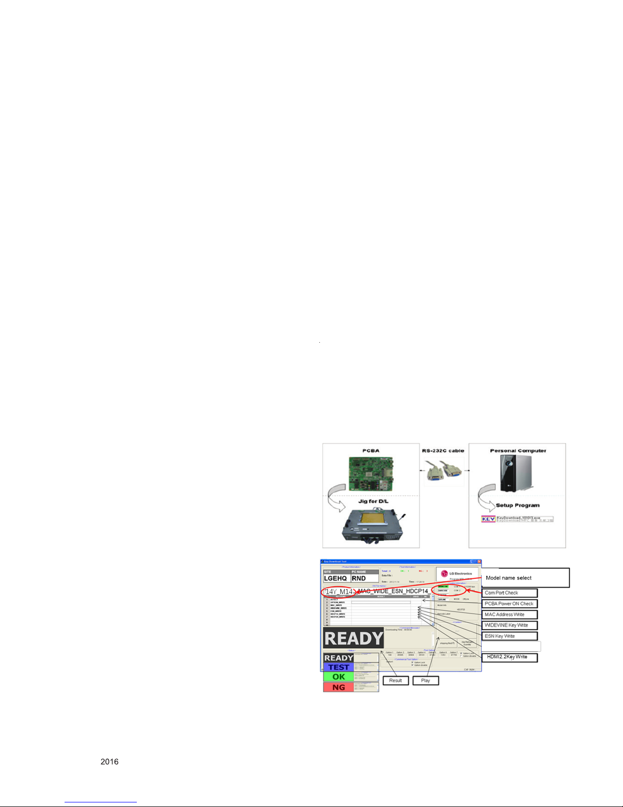
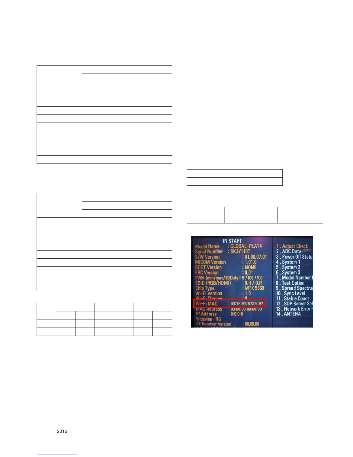
4.2. MAC Address, ESN Key and Widevine
Key download
4.2.1. Equipment & Condition
(1) Play file: keydownload.exe
4.2.2. Communication Port connection
(1) Key Write: Com 1,2,3,4 and 115200 (Baudrate)
(2) Barcode: Com 1,2,3,4 and 9600 (Baudrate)
4.2.3. Download process
(1) Select the download items.
(2) Mode check: Online Only
(3) Check the test process
- US, Canada models: DETECT -> MAC_WRITE ->
WIDEVINE_WRITE
- Korea, Mexico models: DETECT -> MAC_WRITE ->
WIDEVINE_WRITE
(4) Play : START
(5) Check of result: Ready, Test, OK or NG
4.2.4. Communication Port connection
(1) Connect: PCBA Jig -> RS-232C Port == PC -> RS-232C
Port
4.2.5. Download
(1) All models (16Y LCD TV + MAC + Widevine + ESN Key
and HDCP2.2)
4.2.6. Inspection
- In INSTART menu, check these keys.
- 10 -
LGE Internal Use Only
Copyright © LG Electronics. Inc. All rights reserved.
Only for training and service purposes
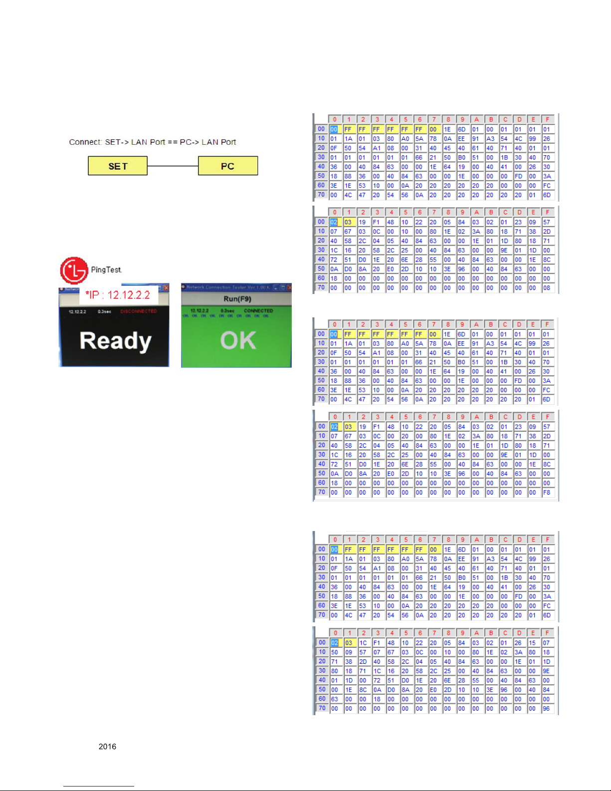
4.3. LAN port Inspection (Ping Test)
4.3.1. Equipment setting
(1) Play the LAN Port Test PROGRAM.
(2) Input IP set up for an inspection to Test Program.
* IP Number : 12.12.2.2.
4.3.2. LAN PORT inspection (PING TEST)
(1) Play the LAN Port Test Program.
(2) connect each other LAN Port Jack.
(3) Play Test (F9) button and confirm OK Message.
(4) remove LAN CABLE
Step 1) Step 3) Check ‘OK’ Signal
4.4. EDID Download
4.4.1 Overview
▪ It is a VESA regulation. A PC or a MNT will display an
optimal resolution through information sharing without any
necessity of user input. It is a realization of “Plug and Play”.
4.4.2 Equipment
▪ Since embedded EDID data is used, EDID download JIG,
HDMI cable and D-sub cable are not need.
▪ Adjust remocon
4.4.3. EDID DATA
4.4.3.1. HD PCM (2D 8bit xvYCC : off) : 32LH570B-UC
(1) HDMI1 (6D , 08)
(2) HDMI2 (6D , F8)
4.4.3.2. HD AC3 (2D 8bit xvYCC : off) : 32LH570B-UC
(1) HDMI1 (6D , 96)
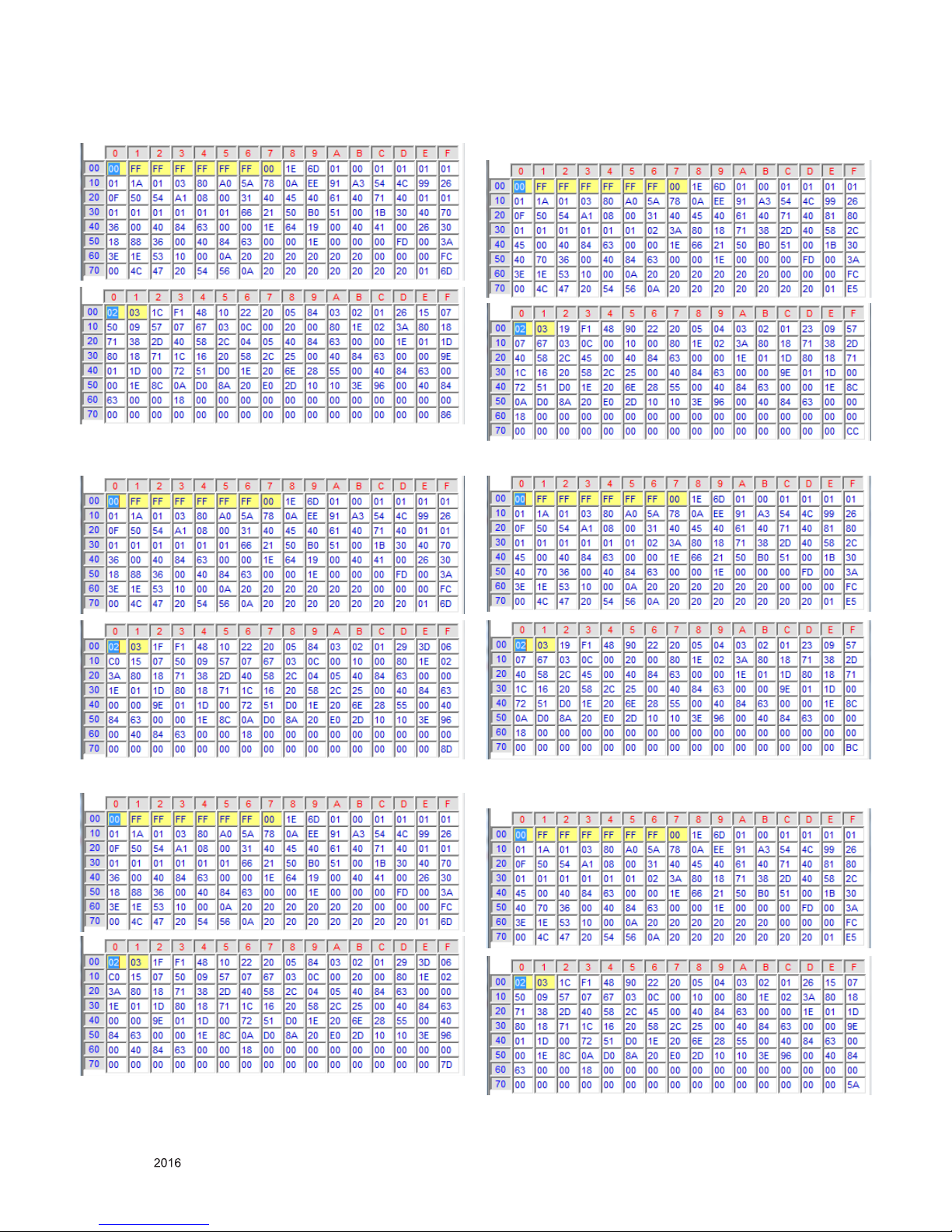
- 11 -
LGE Internal Use Only
Copyright © LG Electronics. Inc. All rights reserved.
Only for training and service purposes
(2) HDMI2 (6D , 86)
4.4.3.3. HD DTS (2D 8bit xvYCC : off) : 32LH570B-UC
(1) HDMI1 (6D , 8D)
(2) HDMI2 (6D , 7D)
4.4.3.4. FHD PCM (2D 8bit xvYCC : off) : 43/49/55LH5700-UD
(1) HDMI1 (E5 , CC)
(2) HDMI2 (E5 , BC)
4.4.3.5. FHD AC3 (2D 8bit xvYCC : off) : 43/49/55LH5700-UD
(1) HDMI1 (E5 , 5A)
- 12 -
LGE Internal Use Only
Copyright © LG Electronics. Inc. All rights reserved.
Only for training and service purposes
(2) HDMI2 (E5 , 4A)
4.4.3.6. FHD DTS (2D 8bit xvYCC : off) : 43/49/55LH5700-UD
(1) HDMI1 (E5 , 51)
(2) HDMI2 (E5 , 41)
5. Final Assembly Adjustment
5.1. White Balance Adjustment
5.1.1. Overview
5.1.1.1. W/B adj. Objective & How-it-works
(1) Objective: To reduce each Panel’s W/B deviation
(2) How-it-works: When R/G/B gain in the OSD is at 192, it
means the panel is at its Full Dynamic Range. In order to
prevent saturation of Full Dynamic range and data, one of
R/G/B is fixed at 192, and the other two is lowered to find
the desired value.
(3) Adj. condition: normal temperature
- Surrounding Temperature: 25±5 °C
- Warm-up time: About 5 Min
- Surrounding Humidity: 20% ~ 80%
- Before White balance adjustment, Keep power on status,
don’t power off
5.1.1.2. Adj. condition and cautionary items
(1) Lighting condition in surrounding area surrounding lighting
should be lower 10 lux. Try to isolate adj. area into dark
surrounding.
(2) Probe location: Color Analyzer (CA-210) probe should be
within 10cm and perpendicular of the module surface
(80°~ 100°)
(3) Aging time
- After Aging Start, Keep the Power ON status during 5
Minutes.
- In case of LCD, Back-light on should be checked using no
signal or Full-white pattern.
5.1.2. Equipment
(1) Color Analyzer: CA-210 (NCG: CH 9 / WCG: CH12 / LED:
CH14)
(2) Adj. Computer (During auto adj., RS-232C protocol is
needed)
(3) Adjust Remocon
(4) Video Signal Generator MSPG-925F 720p/204-Gray
(Model: 217, Pattern: 49)
※ Color Analyzer Matrix should be calibrated using CS-1000
5.1.3. Equipment connection
Color Analyzer
Computer
Pattern Generator
RS-232C
RS-232C
RS-232C
Probe
Signal Source
* If TV internal pattern is used, not needed
- 13 -
LGE Internal Use Only
Copyright © LG Electronics. Inc. All rights reserved.
Only for training and service purposes
5.1.4. Adjustment Command (Protocol)
(1) RS-232C Command used during auto-adj.
RS-232C COMMAND
Explanation
CMD DATA ID
Wb 00 00 Begin White Balance adj.
Wb 00 ff End White Balance adj.
(internal pattern disappears )
(2) Adjustment Map
Adj.
item
Command
(lower caseASCII)
Data Range
(Hex.)
Default
(Decimal)
CMD1 CMD2 MIN MAX
Cool R Gain j g 00 C0 TBD
G Gain j h 00 C0 TBD
B Gain j i 00 C0 TBD
R Cut TBD
G Cut TBD
B Cut TBD
Medium R Gain j a 00 C0 TBD
G Gain j b 00 C0 TBD
B Gain j c 00 C0 TBD
R Cut TBD
G Cut TBD
B Cut TBD
Warm R Gain j d 00 C0 TBD
G Gain j e 00 C0 TBD
B Gain j f 00 C0 TBD
R Cut TBD
G Cut TBD
5.1.5. Adjustment method
5.1.5.1. Auto WB calibration
(1) Set TV in ADJ mode using P-ONLY key (or POWER ON
key)
(2) Place optical probe on the center of the display
- It need to check probe condition of zero calibration before
adjustment.
(3) Connect RS-232C Cable
(4) Select mode in ADJ Program and begin a adjustment.
(5) When WB adjustment is completed with OK message,
check adjustment status of pre-set mode (Cool, Medium,
Warm)
(6) Remove probe and RS-232C cable.
▪ W/B Adj. must begin as start command “wb 00 00” , and
finish as end command “wb 00 ff”, and Adj. offset if need
5.1.5.2. Manual adjustment
(1) Set TV in Adj. mode using POWER ON
(2) Zero Calibrate the probe of Color Analyzer, then place it on
the center of LCD module within 10cm of the surface..
(3) Press ADJ key -> EZ adjust using adj. R/C à 9. White-
Balance then press the cursor to the right (KEY►). When
KEY(►) is pressed 206 Gray internal pattern will be
displayed.
(4) Adjust Cool modes
(i) Fix the one of R/G/B gain to 192 (default data) and
decrease the others.
( If G gain is adjusted over 172 and R and B gain less than
192 , Adjust is O.K.)
(ii) If G gain is less than 172,
Increase G gain by up to 172, and then increase R gain and
G gain same amount of increasing G gain.
(iii) If R gain or B gain is over 255,
Readjust G gain less than 172, Conform to R gain is 255 or
B gain is 255
(5) Adjust two modes (Medium / Warm) Fix the one of R/G/B
gain to 192 (default data) and decrease the others.
(6) Adj. is completed, Exit adjust mode using “EXIT” key on
Remote controller.
5.1.6. Reference (White Balance Adj. coordinate and
color temperature)
(1) Luminance: 204 Gray, 80IRE
(2) Standard color coordinate and temperature using CS-1000
(over 26 inch)
5.1.7. Reference (White Balance Adj. coordinate and
color temperature)
▪ Luminance: 204 Gray
▪ Standard color coordinate and temperature using CS-1000
(over 26 inch)
Mode
Coordinate
Temp △uv
X Y
Cool 0.271 0.270 13,000K 0.0000
Medium 0.286 0.289 9,300K 0.0000
Warm 0.313 0.329 6,500K 0.0000
- 14 -
LGE Internal Use Only
Copyright © LG Electronics. Inc. All rights reserved.
Only for training and service purposes
▪ Standard color coordinate and temperature using
CA-210(CH-14) – by aging time
(1) Normal line in Korea (From January to February)
Aging time
(Min)
Cool Medium Warm
X Y X Y X Y
271 270 286 289 313 329
1 0-2 286 295 301 314 328 354
2 3-5 284 290 299 309 326 349
3 6-9 282 287 297 306 324 346
4 10-19 279 283 294 302 321 342
5 20-35 276 278 291 297 318 337
6 36-49 274 275 289 294 316 334
7 50-79 273 272 288 291 315 331
8 80-119 272 271 287 290 314 330
9 Over 120 271 270 286 289 313 329
▪ Standard color coordinate and temperature using
CA-210(CH-14) – by aging time
(2) Normal line in Korea (From March to December) : LGD
Normal line in Mexico : LGD
Aging time
(Min)
Cool Medium Warm
X Y X Y X Y
271 270 286 289 313 329
1 0-2 282 289 297 308 324 348
2 3-5 281 287 296 306 323 346
3 6-9 279 284 294 303 321 343
4 10-19 277 280 292 299 319 339
5 20-35 275 277 290 296 317 336
6 36-49 274 274 289 293 316 333
7 50-79 273 272 288 291 315 331
8 80-119 272 271 287 290 314 330
9 Over 120 271 270 286 289 313 329
(3) O/S Module(AUO, INX, Sharp, CSOT, BOE)
cool med warm
x y x y x y
spec 271 270 286 289 313 329
target 278 280 293 299 320 339
5.2. Option selection per country
5.2.1. Overview
(1) Tool option selection is only done for models in Non-USA
North America due to rating
(2) Applied model: LA42B Chassis applied to CANADA and
MEXICO
5.2.2. Country Group selection
(1) Press ADJ key on the Adj. R/C, and then select Country
Group Menu
(2) Depending on destination, select US, then on the lower
Country option, select US, CA, MX.
Selection is done using +, - KEY
5.2.3. Tool Option inspection
▪ Press Adj. key on the Adj. R/C, then select Tool option
* Tool option can be reconstructed by Software
5.2.3. Country Group Code
Country Area Option
US 02
5.3. Wi-Fi MAC Address Check
5.3.1. Using RS232 Command
Command Set ACK
Transmission [A][l][][Set ID][][20][Cr] [O][K][x] or [N][G]
5.3.2. Check the menu on in-start
- 15 -
LGE Internal Use Only
Copyright © LG Electronics. Inc. All rights reserved.
Only for training and service purposes
5.6. HDMI ARC Function Inspection
5.6.1. Test equipment
- Optic Receiver Speaker
- MSHG-600 (SW: 1220 ↑)
- HDMI Cable (for 1.4 version)
5.6.2. Test method
(1) Insert the HDMI Cable to the HDMI ARC port from the
master equipment (HDMI1)
(2) Check the sound from the TV Set
(3) Check the Sound from the Speaker or using AV & Optic
TEST program (It’s connected to MSHG-600)
* Remark: Inspect in Power Only Mode and check SW version
in a master equipment
5.7. Ship-out mode check (In-stop)
▪ After final inspection, press In-Stop key of the Adj. R/C and
check that the unit goes to Stand-by mode.
6. AUDIO output check
6.1. Audio input condition
(1) RF input: Mono, 1KHz sine wave signal, 100% Modulation
(2) CVBS, Component: 1KHz sine wave signal (0.4Vrms)
6.2. Specification
No Item Min Typ Max Unit Remark
1 Audio
practical max
Output, L/R
(Distortion=10%
max Output)
4.5
6.0
5.0
6.32
6.0
6.93WVrms
(1) Measurement
condition
- EQ/AVL/Clear
Voice: Off
(2) Speaker (6Ω
Impedance)
(3) 49/43LH57
2 2.7
4.03
3.0
4.24
3.6
4.64WVrms
(1) Measurement
condition
- EQ/AVL/Clear
Voice: Off
(2) Speaker (6Ω
Impedance)
(3) 32LH57
7. GND and HI-POT Test
7.1. GND & HI-POT auto-check preparation
(1) Check the POWER CABLE and SIGNAL CABE insertion
condition
7.2. GND & HI-POT auto-check
(1) Pallet moves in the station. (POWER CORD / AV CORD is
tightly inserted)
(2) Connect the AV JACK Tester.
(3) Controller (GWS103-4) on.
(4) GND Test (Auto)
- If Test is failed, Buzzer operates.
- If Test is passed, execute next process (Hi-pot test).
(Remove A/V CORD from A/V JACK BOX)
(5) HI-POT test (Auto)
- If Test is failed, Buzzer operates.
- If Test is passed, GOOD Lamp on and move to next
process automatica
- 16 -
LGE Internal Use Only
Copyright © LG Electronics. Inc. All rights reserved.
Only for training and service purposes
7.3. Checkpoint
(1) Test voltage
Products/Model TV
2Poles Other 3000V(AC)/
4242V(DC)
3Poles Other 1500V(AC)/
2121V(DC)
Cut off current 100mA(AC)/100mA(DC)
Earth Continutiy test
(3Poles only)
≤0.1Ὼ at 25A/1 sec
(2) TEST time: 1 second
(3) TEST POINT
- GND Test = POWER CORD GND and SIGNAL CABLE GND.
- Hi-pot Test = POWER CORD GND and LIVE & NEUTRAL.
(4) LEAKAGE CURRENT: At 0.5mArms
9. USB S/W Download
(optional, Service only)
(1) Put the USB Stick to the USB socket
(2) Automatically detecting update file in USB Stick
- If your downloaded program version in USB Stick is lower
than that of TV set, it didn’t work. Otherwise USB data is
automatically detected.
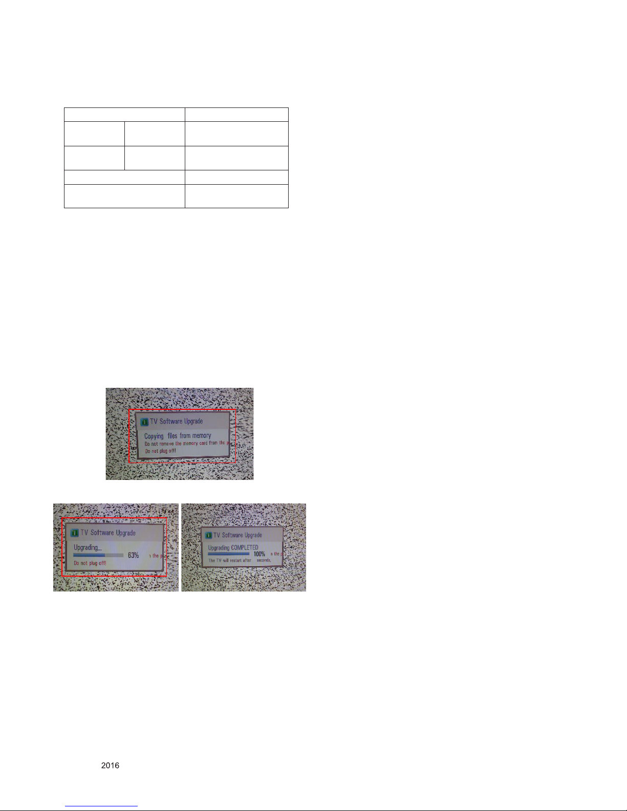
(3) Show the message “Copying files from memory”
(4) Updating is staring.
(5) Updating Completed, The TV will restart automatically
(6) If your TV is turned on, check your updated version and
Tool option.
* If downloading version is more high than your TV have, TV
can lost all channel data. In this case, you have to channel
recover. If all channel data is cleared, you didn’t have a DTV/
ATV test on production line.
* After downloading, TOOL OPTION setting is needed again.
(1) Push "IN-START" key in service remote controller.
(2) Select "Tool Option 1" and Push “OK” button.
(3) Punch in the number. (Each model has their number.)
10. Optional adjustments
10.1. Manual White balance Adjustment
10.1.1. Adj. condition and cautionary items
(1) Lighting condition in surrounding area surrounding lighting
should be lower 10 lux. Try to isolate adj. area into dark
surrounding.
(2) Probe location: Color Analyzer (CA-210) probe should be
within 10cm and perpendicular of the module surface
(80°~ 100°)
(3) Aging time
- After Aging Start, Keep the Power ON status during 5
Minutes.
- In case of LCD, Back-light on should be checked using no
signal or Full-white pattern
10.1.2. Equipment
(1) Color Analyzer: CA-210 (NCG: CH 9 / WCG: CH12 / LED:
CH14)
(2) Adj. Computer (During auto adj., RS-232C protocol is
needed)
(3) Adjust Remocon
(4) Video Signal Generator MSPG-925F 720p/216-Gray
(Model: 217, Pattern: 78)
10.1.3. Adjustment
(1) Set TV in Adj. mode using POWER ON
(2) Zero Calibrate the probe of Color Analyzer, then place it on
the center of LCD module within 10cm of the surface.
(3) Press ADJ key -> EZ adjust using adj. R/C -> 6. White-
Balance then press the cursor to the right (KEY►).
When KEY(►) is pressed 216 Gray internal pattern will be
displayed.
(4) One of R Gain / G Gain / B Gain should be fixed at 192,
and the rest will be lowered to meet the desired value.
(5) Adj. is performed in COOL, MEDIUM, WARM 3 modes of
color temperature.
▪ If internal pattern is not available, use RF input. In EZ Adj.
menu 6.White Balance, you can select one of 2 Test-pattern:
ON, OFF. Default is inner(ON). By selecting OFF, you can
adjust using RF signal in 216 Gray pattern.
- 17 -
LGE Internal Use Only
Copyright © LG Electronics. Inc. All rights reserved.
Only for training and service purposes
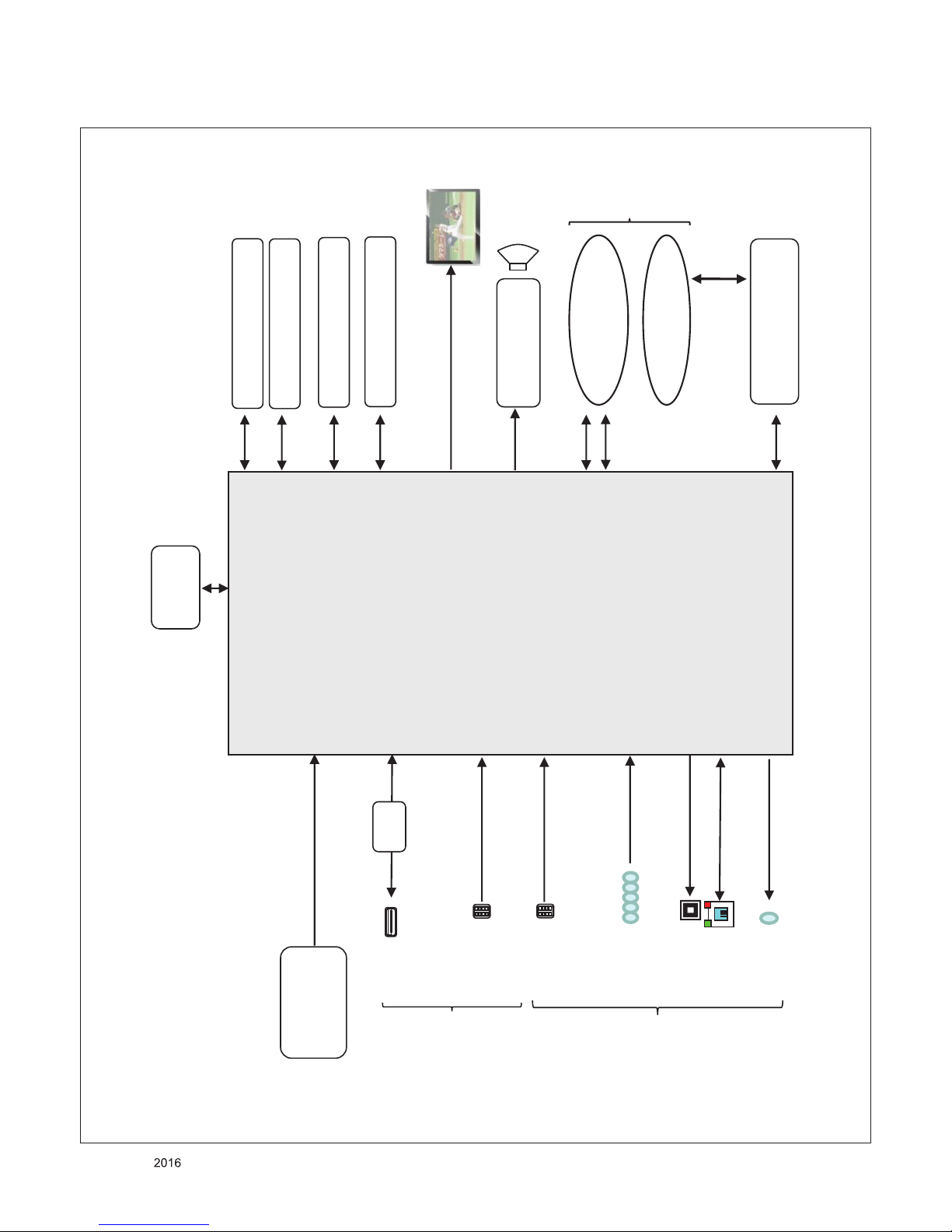
BLOCK DIAGRAM
M2
(NON MCP)
Audio AM P
Digital Demod
IF (+/-)
Sub Micom
(R5F100GEAFB)
IR / KEY
IR
KEY
I2C
HDMI
MUX
LVDS
USB
SPDIF OUT
ETHERNET
USB1
OCP
1.5A
HDMI1
(ARC)
REAR
OPTIC
LAN
51P
DDR3 1866 2Gb x16
X_TAL
24MHz
WIFI
SUB
ASSY
USB_WIFI
Tuner
DDR3 1866 2Gb x16
HDMI2
SIDE
CVBS/YPbPr
AV/COMP
REAR
EEPROM (256Kb)
eMMC 5.0 (4GB)
I2S
I2C
I2C
I2C
Analog Demod
* HD Model : 30P
RS-232
RS-232
* RS-232 US Only
- 18 -
LGE Internal Use OnlyCopyright © LG Electronics. Inc. All rights reserved.
Only for training and service purposes
EXPLODED VIEW
Many electrical and mechanical parts in this chassis have special safety-related characteristics. These
parts are identified by in the Schematic Diagram and EXPLODED VIEW.
It is essenti al that these spec ial safety parts s hould be replaced with the same components a s
recommended in this manual to prevent, Shock, Fire, or other Hazards.
Do not modify the original design without permission of manufacturer.
IMPORTANT SAFETY NOTICE
400
570
540
521
500
600
522
LV1
200
900
A2
700
120
720
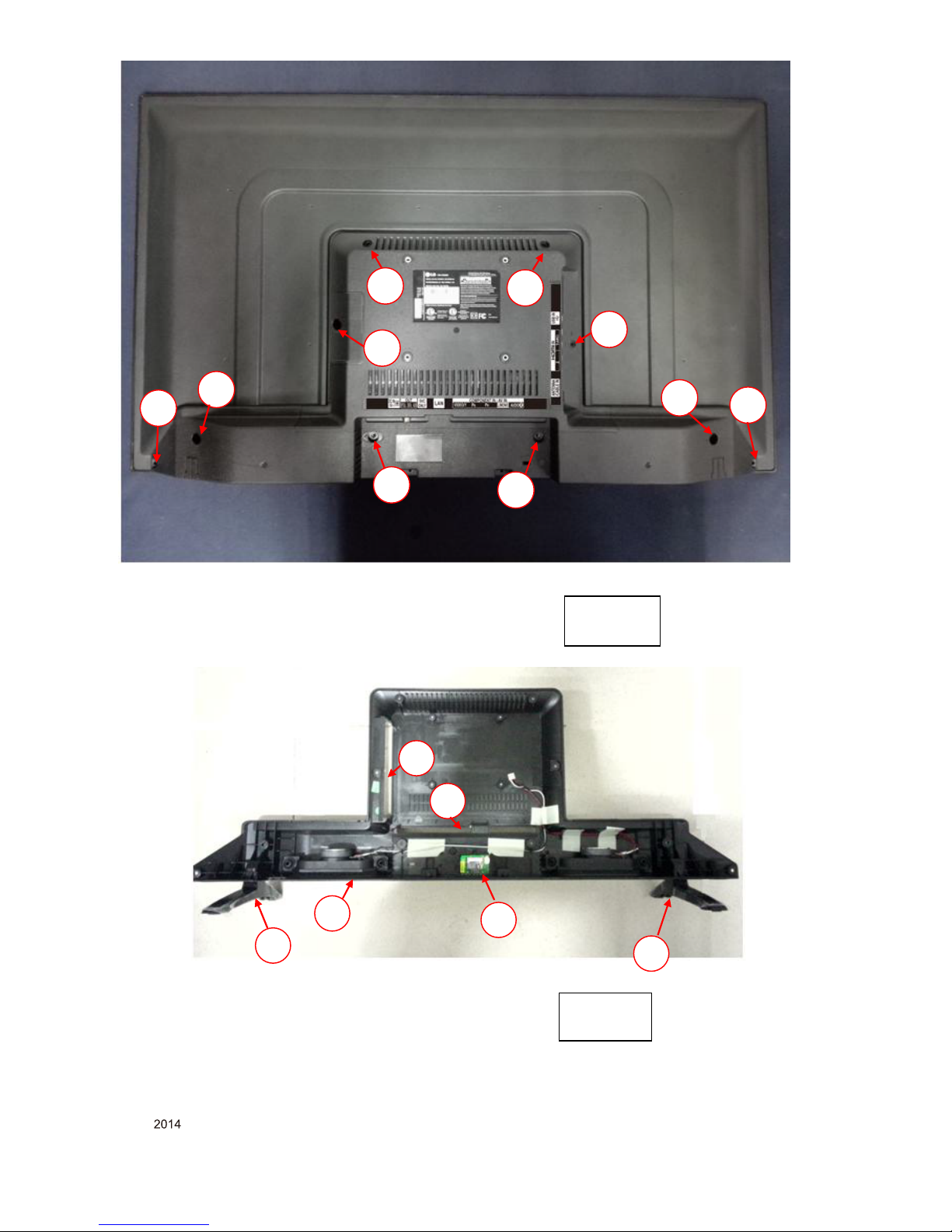
Product Disassembly Process
List the basic steps that should typically be followed to remove components and materials requiring
selective treatment:
1.OPTIONAL: Depending upon the complexity of the disassembly process, a graphic depicting the locations
of items contained within the product which require selective treatment
(with descriptions and arrows identifying locations) can be inserted below:
1 Unlock screw (“A-10EA”) to separate back cover assembly.
[Fig.1]
2
Separate speaker assembly from back cover.
Separate the cushion (B,C,D) from backcover.
Separate the WIFI board(L) from backcover.
Unlock screw (”E-2EA”) to separate the base.
[Fig.2]
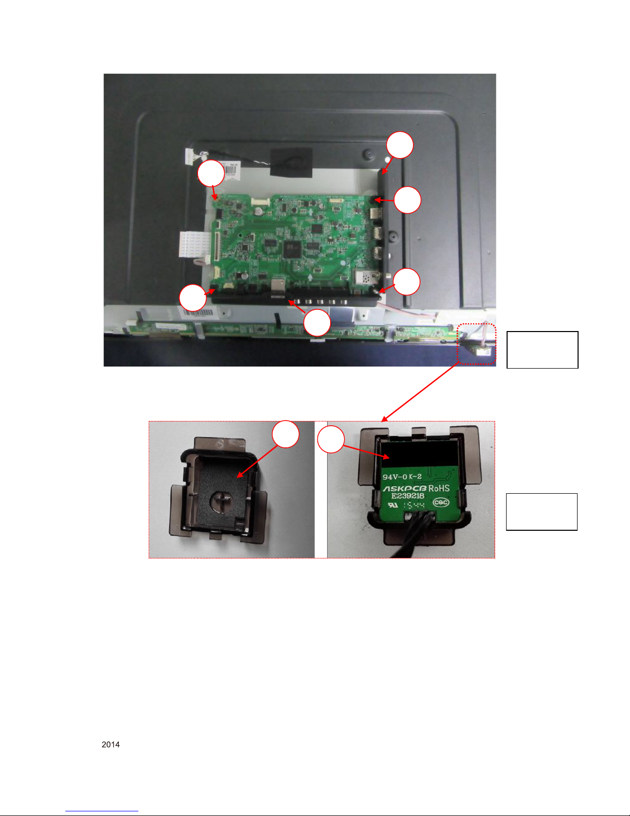
3 Unlock screw (”F-4EA”) to sepparate main board and AV bracket (H, I). [Fig
.3]
4
Separate the receive assembly from front cover;
Separate the cushion (J) from receive board;
Separate the receive board from IR LENS;
Separate the PC sheet (K) from IR LENS.
[Fig.4]
- 19 -
LGE Internal Use OnlyCopyright © LG Electronics. Inc. All rights reserved.
Only for training and service purposes
- 20 -
LGE Internal Use OnlyCopyright © LG Electronics. Inc. All rights reserved.
Only for training and service purposes
A
A
A
A
A
A
A
A
A
A
Fig.1
Fig.2
B
C
E
D
E
L
- 21 -
LGE Internal Use OnlyCopyright © LG Electronics. Inc. All rights reserved.
Only for training and service purposes
J
K
F
F
F
F
H
I
Fig.3
Fig.4
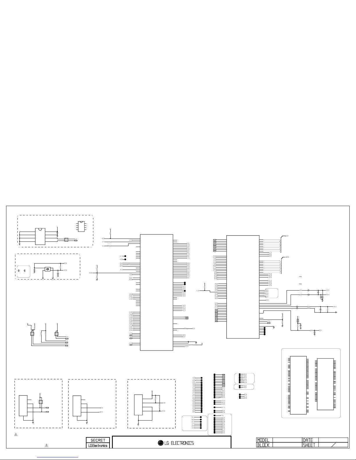
THE SYMBOL MARK OF THIS SCHEMETIC DIAGRAM INCORPORATES
SPECIAL FEATURES IMPORTANT FOR PROTECTION FROM X-RADIATION.
FIRE AND ELECTRICAL SHOCK HAZARDS, WHEN SERVICING IF IS
ESSENTIAL THAT ONLY MANUFACTURES SPECIFIED PARTS BE USED FOR
THE CRITICAL COMPONENTS IN THE SYMBOL MARK OF THE SCHEMETIC.
TPO_DATA[6]
TPI_DATA[5]
TPI_DATA[2]
TPI_DATA[0]
TPO_DATA[7]
TPI_DATA[7]
TPI_DATA[6]
TPO_DATA[4]
TPO_DATA[5]
TPI_DATA[4]
TPI_DATA[3]
TPI_DATA[1]
TPO_DATA[0]
TPO_DATA[2]
TPO_DATA[3]
TPO_DATA[1]
R136
PWM_DIM2
100
FE_DEMOD1_TS_DATA[3]
TP161
CI_OE#
5V_DET_HDMI_1
TXA2N
EB_ADDR[4]
IC100
AT24C256C-SSHL-T
NVRAM_ATMEL
3
A2
2
A1
4
GND
1
A0
5
SDA
6
SCL
7
WP
8
VCC
FE_DEMOD1_TS_DATA[7]
TP125
EMMC_DATA[0]
C120
0.1uF
IF_FILTER
EB_ADDR[9]
USB_CTL1
TP113
TP198
R135
100
EB_ADDR[14]
TP149
BIT4
TXB1P
TP142
FE_DEMOD1_TS_SYNC
DDTS_TX
I2C_SDA1
EB_ADDR[5]
C119
0.1uF
IF_FILTER
TPI_CLK
TP343
EB_DATA[0]
TP137
R102
47
TU_SIF
EB_ADDR[5]
TP150
CI_OE#
BIT6
TXA3N
XTAL_IN
/TU_RESET1
EB_DATA[3]
CI_CE1#
TP133
R145 0
TUNER_IF_0ohm
I2C_SDA1
TP344
TPO_VAL
TPO_CLK
C103 0.1uF
TU_SIF
FE_DEMOD1_TS_CLK
TP163
I2C_SCL1
BIT7
TXB3N
EB_ADDR[8]
TPO_VAL
DDTS_RX
TP135
EB_DATA[1]
R146
0
TUNER_IF_0ohm
TP119
TP345
XTAL_OUT
EB_ADDR[10]
C110
1000pF
OPT
CI_RESET
IC101
LGE6322(MSD93F2G, w/oT2S2 : M2)
EAN64207702
NON-MCP
PWM0
A25
PWM1
B26
PWM2
B25
PWM3
C24
PWM_PM
D7
SAR0
E6
SAR1
E5
SAR2
F5
SAR3
F6
SAR4
G5
PM_SPI_CK
B2
PM_SPI_DI
A2
PM_SPI_DO
B1
NC_13
H8
GPIO_PM[6]/(SPI-CZ1N)
C1
GPIO_PM[10]/(SPI-CZ2N)
C2
PM_SPI_HOLDN(GPIO)
A3
PM_SPI_WPN/(GPIO)
C3
DDCA_CK
D5
DDCA_DA
D6
DDCR_CK
J21
DDCR_DA
H21
UART_TX2
H22
UART_RX2
H23
GPIO7/TX1
E22
GPIO8/RX1
F21
GPIO11/TX3
E20
GPIO12/RX3
F20
PCM2_WAIT_N/TX4
AB6
PCM2_IRQA_N
M23
PCM2_CE_N
M22
NC_14
AC6
GPIO_PM[0]
J5
GPIO_PM[1](PM_UART)
E8
GPIO_PM[2]
M4
GPIO_PM[3]
J6
GPIO_PM[4]
N4
GPIO_PM[5](PM_UART)
F8
GPIO_PM[7]
K5
GPIO_PM[8]
K6
GPIO_PM[9]
L6
GPIO_PM[11]/(PM_UART)
C4
GPIO_PM[12](PM_UART)
B4
GPIO_PM[15]
B3
GPIO17/SCKM0
K21
GPIO18/SDAM0
L22
GPIO15/SCKM2
K22
GPIO14/SDAM2
L21
TCON5/SCKM4
J22
TCON4/SDAM4
K23
R_ODD[7]/LVB0N
G25
R_ODD[6]/LVB0P
G24
R_ODD[5]/LVB1N
H25
R_ODD[4]/LVB1P
H24
R_ODD[3]/LVB2N
J25
R_ODD[2]/LVB2P
J26
R_ODD[1]/LVBCLKN
J24
R_ODD[0]/LVBCLKP
K26
G_ODD[7]/LVB3N
K25
G_ODD[6]/LVB3P
K24
G_ODD[5]/LVB4N
L25
G_ODD[4]/LVB4P
L24
G_ODD[3]/LVA0N
M25
G_ODD[2]/LVA0P
M26
G_ODD[1]/LVA1N
M24
G_ODD[0]/LVA1P
N26
B_ODD[7]/LVA2N
N25
B_ODD[6]/LVA2P
N24
B_ODD[5]/LVACLKN
P25
B_ODD[4]/LVACLKP
P24
B_ODD[3]/LVA3N
R25
B_ODD[2]/LVA3P
R26
B_ODD[1]/LVA4N
R24
B_ODD[0]/LVA4P
T26
SPI1_DI
F25
SPI1_CK
F26
GPIO6
L23
GPIO9
N23
GPIO10
N22
VSYNC_LIKE
F24
TS2_D[1]
AA23
TS2_D[3]
Y23
TS2_D[2]
AA22
LINEIN_L3
Y2
LINEIN_R3
Y4
TS2_D[4]
Y22
TS2_D[5]
W23
TS2_D[6]
W22
TS2_D[7]
W21
NC_15
AD2
NC_16
AD1
IRIN
C5
VID0
F7
VID1
E7
XTAL_IN
AE1
XTAL_OUT
AF2
GND_1
M11
GND_2
M7
NC_17
J7
RESET
D8
EB_ADDR[12]
BIT5
TXACLKP
EMMC_DATA[1]
CI_CD#
JK101
12507WS-04L
DEBUG
1
2
3
4
5
TP106
EB_DATA[1]
AGP
TPI_DATA[0-7]
TP346
TPO_SYNC
EB_ADDR[7]
R103 47
TU_SIF
EB_DATA[6]
IC101
LGE6322(MSD93F2G, w/oT2S2 : M2)
NON-MCP
PCM_D[0]
T25
PCM_D[1]
AB26
PCM_D[2]
Y24
PCM_D[3]
P21
PCM_D[4]
R22
PCM_D[5]
AA24
PCM_D[6]
T21
PCM_D[7]
V21
PCM_A[0]
V26
PCM_A[1]
V23
PCM_A[2]
N21
PCM_A[3]
U23
PCM_A[4]
W26
PCM_A[5]
AA25
PCM_A[6]
U22
PCM_A[7]
V25
PCM_A[8]
V22
PCM_A[9]
V24
PCM_A[10]
P22
PCM_A[11]
U21
PCM_A[12]
W25
PCM_A[13]
Y25
PCM_A[14]
AB24
PCM_IRQA_N
T23
PCM_OE_N
R21
PCM_IORD_N
T22
PCM_CE_N
AB25
PCM_WE_N
AA26
PCM_CD_N
U25
PCM_RESET
T24
PCM_REG_N
P23
PCM_IOWR_N
U24
PCM_WAIT_N
W24
EMMC_IO[8](EMMC_DS)(NAND_ALE)
AD26
EMMC_IO[10](EMMC_CLK)(NAND_RBZ)
AC25
EMMC_IO[9](EMMC_CMD)
AC24
EMMC_IO[11](EMMC_RSTN)
AD25
EMMC_IO[0](EMMC_D0)(NAND_CEZ)
AF24
EMMC_IO[1](EMMC_D1)(NAND_WPZ)
AE24
EMMC_IO[2](EMMC_D2)(NAND_CLE)
AF25
EMMC_IO[3]/(EMMC_D3)(NAND_DQS)
AD23
EMMC_IO[4](EMMC_D4)(NAND_REZ)
AF23
EMMC_IO[5](EMMC_D5)(NAND_CE1Z)
AE23
EMMC_IO[6](EMMC_D6)(NAND_WEZ)
AE26
EMMC_IO[7](EMMC_D7)
AE25
TS1_D[0]
AA21
TS1_D[1]
W20
TS1_D[2]
AB20
TS1_D[3]
AB19
TS1_D[4]
W19
TS1_D[5]
AB21
TS1_D[6]
AA19
TS1_D[7]
AA20
TS1_CLK
Y20
TS1_VLD
Y21
TS1_SYNC
Y19
TS0_D[0]
AF20
TS0_D[1]
AC21
TS0_D[2]
AE21
TS0_D[3]
AF21
TS0_D[4]
AC19
TS0_D[5]
AD20
TS0_D[6]
AE20
TS0_D[7]
AE19
TS0_CLK
AD19
TS0_VLD
AE22
TS0_SYNC
AD21
TS2_SYNC
AB22
TS2_CLK
AC22
TS2_VLD
AC23
TS2_D[0]
AB23
NC_1
AC3
NC_2
AB2
NC_3
AB3
NC_4
AA1
NC_5
AC2
NC_6
AC4
VIFP
AF4
VIFM
AE4
SIFP
AF5
SIFM
AE5
IFAGC
AD4
TGPIO0
AB4
TGPIO1
AD5
TGPIO2/SCKM1
AE3
TGPIO3/SDAM1
AD3
NC_7
P10
NC_8
N10
NC_9
N11
NC_10
P11
NC_11
R10
NC_12
R11
EB_ADDR[1]
EMMC_STRB
TXB2P
EB_ADDR[11]
EB_ADDR[4]
+3.3V_SB
I2C_SCL2
EB_ADDR[1]
+3.3V_NORMAL
EB_DATA[4]
TP347
+3.3V_TUNER
TP143
C102 0.1uF
TU_SIF
TP147
IC101-*1
LGE6321(MSD93F2GW, w/ T2S2 : M2)
MCP
PCM_D[0]
T25
PCM_D[1]
AB26
PCM_D[2]
Y24
PCM_D[3]
P21
PCM_D[4]
R22
PCM_D[5]
AA24
PCM_D[6]
T21
PCM_D[7]
V21
PCM_A[0]
V26
PCM_A[1]
V23
PCM_A[2]
N21
PCM_A[3]
U23
PCM_A[4]
W26
PCM_A[5]
AA25
PCM_A[6]
U22
PCM_A[7]
V25
PCM_A[8]
V22
PCM_A[9]
V24
PCM_A[10]
P22
PCM_A[11]
U21
PCM_A[12]
W25
PCM_A[13]
Y25
PCM_A[14]
AB24
PCM_IRQA_N
T23
PCM_OE_N
R21
PCM_IORD_N
T22
PCM_CE_N
AB25
PCM_WE_N
AA26
PCM_CD_N
U25
PCM_RESET
T24
PCM_REG_N
P23
PCM_IOWR_N
U24
PCM_WAIT_N
W24
EMMC_IO[8](EMMC_DS)(NAND_ALE)
AD26
EMMC_IO[10](EMMC_CLK)(NAND_RBZ)
AC25
EMMC_IO[9](EMMC_CMD)
AC24
EMMC_IO[11](EMMC_RSTN)
AD25
EMMC_IO[0](EMMC_D0)(NAND_CEZ)
AF24
EMMC_IO[1](EMMC_D1)(NAND_WPZ)
AE24
EMMC_IO[2](EMMC_D2)(NAND_CLE)
AF25
EMMC_IO[3]/(EMMC_D3)(NAND_DQS)
AD23
EMMC_IO[4](EMMC_D4)(NAND_REZ)
AF23
EMMC_IO[5](EMMC_D5)(NAND_CE1Z)
AE23
EMMC_IO[6](EMMC_D6)(NAND_WEZ)
AE26
EMMC_IO[7](EMMC_D7)
AE25
TS1_D[0]
AA21
TS1_D[1]
W20
TS1_D[2]
AB20
TS1_D[3]
AB19
TS1_D[4]
W19
TS1_D[5]
AB21
TS1_D[6]
AA19
TS1_D[7]
AA20
TS1_CLK
Y20
TS1_VLD
Y21
TS1_SYNC
Y19
TS0_D[0]
AF20
TS0_D[1]
AC21
TS0_D[2]
AE21
TS0_D[3]
AF21
TS0_D[4]
AC19
TS0_D[5]
AD20
TS0_D[6]
AE20
TS0_D[7]
AE19
TS0_CLK
AD19
TS0_VLD
AE22
TS0_SYNC
AD21
TS2_SYNC
AB22
TS2_CLK
AC22
TS2_VLD
AC23
TS2_D[0]
AB23
NC_1
AC3
NC_2
AB2
NC_3
AB3
NC_4
AA1
NC_5
AC2
NC_6
AC4
VIFP
AF4
VIFM
AE4
SIFP
AF5
SIFM
AE5
IFAGC
AD4
TGPIO0
AB4
TGPIO1
AD5
TGPIO2/SCKM1
AE3
TGPIO3/SDAM1
AD3
NC_7
P10
NC_8
N10
NC_9
N11
NC_10
P11
NC_11
R10
NC_12
R11
TP112
TXB1N
I_P_SoC
TP131
I2C_SDA2
R148 10K
OPT
TP128
MCP_SCL
EMMC_DATA[6]
TP145
TP121
CI_WAIT#
IC101-*1
LGE6321(MSD93F2GW, w/ T2S2 : M2)
EAN64207701
MCP
PWM0
A25
PWM1
B26
PWM2
B25
PWM3
C24
PWM_PM
D7
SAR0
E6
SAR1
E5
SAR2
F5
SAR3
F6
SAR4
G5
PM_SPI_CK
B2
PM_SPI_DI
A2
PM_SPI_DO
B1
NC_13
H8
GPIO_PM[6]/(SPI-CZ1N)
C1
GPIO_PM[10]/(SPI-CZ2N)
C2
PM_SPI_HOLDN(GPIO)
A3
PM_SPI_WPN/(GPIO)
C3
DDCA_CK
D5
DDCA_DA
D6
DDCR_CK
J21
DDCR_DA
H21
UART_TX2
H22
UART_RX2
H23
GPIO7/TX1
E22
GPIO8/RX1
F21
GPIO11/TX3
E20
GPIO12/RX3
F20
PCM2_WAIT_N/TX4
AB6
PCM2_IRQA_N
M23
PCM2_CE_N
M22
NC_14
AC6
GPIO_PM[0]
J5
GPIO_PM[1](PM_UART)
E8
GPIO_PM[2]
M4
GPIO_PM[3]
J6
GPIO_PM[4]
N4
GPIO_PM[5](PM_UART)
F8
GPIO_PM[7]
K5
GPIO_PM[8]
K6
GPIO_PM[9]
L6
GPIO_PM[11]/(PM_UART)
C4
GPIO_PM[12](PM_UART)
B4
GPIO_PM[15]
B3
GPIO17/SCKM0
K21
GPIO18/SDAM0
L22
GPIO15/SCKM2
K22
GPIO14/SDAM2
L21
TCON5/SCKM4
J22
TCON4/SDAM4
K23
R_ODD[7]/LVB0N
G25
R_ODD[6]/LVB0P
G24
R_ODD[5]/LVB1N
H25
R_ODD[4]/LVB1P
H24
R_ODD[3]/LVB2N
J25
R_ODD[2]/LVB2P
J26
R_ODD[1]/LVBCLKN
J24
R_ODD[0]/LVBCLKP
K26
G_ODD[7]/LVB3N
K25
G_ODD[6]/LVB3P
K24
G_ODD[5]/LVB4N
L25
G_ODD[4]/LVB4P
L24
G_ODD[3]/LVA0N
M25
G_ODD[2]/LVA0P
M26
G_ODD[1]/LVA1N
M24
G_ODD[0]/LVA1P
N26
B_ODD[7]/LVA2N
N25
B_ODD[6]/LVA2P
N24
B_ODD[5]/LVACLKN
P25
B_ODD[4]/LVACLKP
P24
B_ODD[3]/LVA3N
R25
B_ODD[2]/LVA3P
R26
B_ODD[1]/LVA4N
R24
B_ODD[0]/LVA4P
T26
SPI1_DI
F25
SPI1_CK
F26
GPIO6
L23
GPIO9
N23
GPIO10
N22
VSYNC_LIKE
F24
TS2_D[1]
AA23
TS2_D[3]
Y23
TS2_D[2]
AA22
LINEIN_L3
Y2
LINEIN_R3
Y4
TS2_D[4]
Y22
TS2_D[5]
W23
TS2_D[6]
W22
TS2_D[7]
W21
NC_15
AD2
NC_16
AD1
IRIN
C5
VID0
F7
VID1
E7
XTAL_IN
AE1
XTAL_OUT
AF2
GND_1
M11
GND_2
M7
NC_17
J7
RESET
D8
VDD33
TXA2P
I_N_SoC
I2C_SCL3
TP123
R149 10K
OPT
EB_ADDR[0]
TP118
AR104
3.3K
MCP DEBUG
EB_ADDR[13]
IF_N
FE_DEMOD1_TS_DATA[5]
EMMC_DATA[7]
TU_SIF
EB_DATA[7]
TXB3P
+3.3V_NORMAL
EMMC_DATA[4]
R150
0
OPT
TXB0P
Q_P_SoC
CI_WAIT#
EB_DATA[5]
I2C_SCL1
EMMC_DATA[5]
EB_DATA[0]
TP144
PWM_DIM2
TP148
TP141
TXA1N
+3.3V_NORMAL
FE_DEMOD1_TS_DATA[0]
R138
10K
NON_EU
TXA1P
Q_N_SoC
CI_REG#
JK100
12507WS-04L
DEBUG
1
2
3
4
5
TP199
EB_ADDR[10]
JK102
12507WS-04L
MCP DEBUG
1
2
3
4
5
TP110
IF_AGC
+3.3V_NORMAL
I2C_SDA3
PCM_5V_CTL
EMMC_CMD
I2C_SDA2
CI_IORD#
WOL_WAKE_UP_SOC
TXA0P
LNB_TX
EB_ADDR[3]
DDCA_CK
CI_CD#
C112
0.1uF
MCP_SDA
TP108
R144
10K
IF_FILTER
TP146
TPI_VAL
R152 33
I2C_SDA1
I2C_SCL2
EB_DATA[7]
TXA0N
IF_AGC_S_SOC
TPI_VAL
DDCA_DA
CI_REG#
R115
1.8K
MCP_SCL
TPI_SYNC
TP115
EB_DATA[3]
R105
10K
OPT
TPO_DATA[0-7]
I2C_SDA3
+3.3V_NORMAL
EB_ADDR[13]
TP120
TXBCLKN
IF_AGC_S_SOC
TP130
DDCA_CK
EB_DATA[5]
R116
1.8K
MCP_SDA
CI_IREQ#
AMP_RESET_N
C123
33pF
IF_FILTER_CAP
EB_DATA[2]
TP140
R106
10K
OPT
TP116
I2C_SCL3
+3.3V_NORMAL
EB_DATA[4]
EB_ADDR[3]
LNB_TX
TP117
DDCA_DA
TP109
IC100-*1
BR24G256FJ-3
NVRAM_ROHM
3
A2
2
A1
4
GND
1
A0
5
SDA
6
SCL
7
WP
8
VCC
R117
300
1%
OPT
TPO_SYNC
TP127
C122
33pF
IF_FILTER_CAP
TP111
EB_ADDR[2]
EB_DATA[6]
I2C_SDA4
+3.3V_NORMAL
CI_RESET
FE_DEMOD1_TS_DATA[1]
C124
0.022uF
16V
IF_FILTER
I_P_SoC
CI_IOWR#
DDTS_TX
PCM_5V_CTL
FE_DEMOD1_TS_DATA[2]
EB_DATA[2]
C118
0.1uF
IF_FILTER
TP126
CI_IOWR#
+3.3V_SB
TPI_SYNC
I2C_SCL4
R140
0
XTAL_IN
VID_CTRL
I_N_SoC
CI_IREQ#
DDTS_RX
TXB0N
TPI_CLK
TP138
TPO_DATA[0-7]
AR101
33
EMMC_DATA[2]
/USB_OCD1
R141
0
OPT
SOC_TX
R153 33
Q_P_SoC
EB_ADDR[2]
M_RFModule_RESET
TXB2N
FE_DEMOD1_TS_VAL
EMMC_CLK
R147
0
IF_FILTER
PWM_DIM
EB_ADDR[6]
AR102
3.3K
EB_ADDR[6]
AV_CVBS_DET
TPI_DATA[0-7]
CI_IORD#
R101
10K
T2/S2
Q_N_SoC
EB_ADDR[0]
COMP2_DET
TXACLKN
XTAL_OUT
EMMC_RST
FE_DEMOD1_TS_DATA[4]
IF_P
EB_ADDR[12]
CI_WE#
AR103
3.3K
EB_ADDR[9]
USB_CTL2
CI_WE#
EB_ADDR[14]
R104
10K
OPT
TP160
TP134
SOC_RESET
TXA3P
R137
1M
TP114
EB_ADDR[7]
CI_CE1#
+3.3V_SB
RETENTION_DISABLE
SOC_RX
/USB_OCD2
I2C_SCL1
EMMC_DATA[3]
TP132
TP162
TP139
5V_DET_HDMI_3
TXBCLKP
X100
24MHz
SUNNY ELECTRONICS CORPORATION
3225
4
GND_2
1
X-TAL_1
2
GND_13X-TAL_2
EB_ADDR[11]
C121
100pF
OPT
TPO_CLK
EB_ADDR[8]
INSTANT_BOOT
TP136
5V_DET_HDMI_2
TP129
FE_DEMOD1_TS_DATA[6]
I2C_SDA4
TP164
I2C_SCL4
TP165
C100-*1
8pF
50V
0CZZB00024A
8pF
C101-*1
8pF
50V
8pF
TP166
5V_DET_HDMI_2
/USB_OCD2
TP167
USB_CTL2
TP168
R145-*1
100
TUNER_IF_100ohm
R146-*1
100
TUNER_IF_100ohm
L102
BLM15PX121SN1
IF_FILTER
PWM_DIM2
TP1014
HP_LOUT_SOC
TP1012
HP_ROUT_SOC
HP_DET
TP1013
TP1011
TXB0P
TP1007
TXB1P
TP1006
TP1003
TP1001
TXB3N
TP1010
TP1008
TXB3P
TP1004
TP1002
TP1005
TXB0N
TP1009
TXBCLKN
TXBCLKP
TXB1N
TXB2P
TXB2N
M_RFModule_RESET
TP1015
EYE_SDA
TP1016
EYE_SCL
TP1017
MIU0_STR_PD
MIU1_STR_PD
MIU0_STR_PD
MIU1_STR_PD
TP1030
TP1031
C101
10pF
50V
10pF
C100
10pF
50V
10pF
+3.3V_NORMAL
R154
10K
OPT
2015.10.02
1
MAIN1
16Y_M2
FOR BRAZIL Energy Regulation
need to ADD SILK
"LJ6 CHASSIS"
P/NO
MCP : EAN64207701 (MSD93F2GW)
NON MCP : EAN64207702 (MSD93F2G)
SATELLITE
SATELLITE
MCP for T2/S2
NVRAM
I2C_1 : AMP, L/D, NVM, TCON
I2C_2 : TUNER
I2C_3 : MICOM
I2C_4 : S/Demod,T2/Demod, LNB ==> only for LNB - Satellite Model
Write Protection
- Low : Normal Operation
- High : Write Protection
I2C
Close to MSTAR
DDTS_Debug
Mstart Debug
MCP Debug
X-TAL
SATELLITE - LNB only
10pF Option
FOR LH57 HD MODEL
FOR LH57 EU MODEL
Copyright © 2016 LG Electronics Inc. All rights reserved.
Only for training and service purposes
LGE Internal Use Only
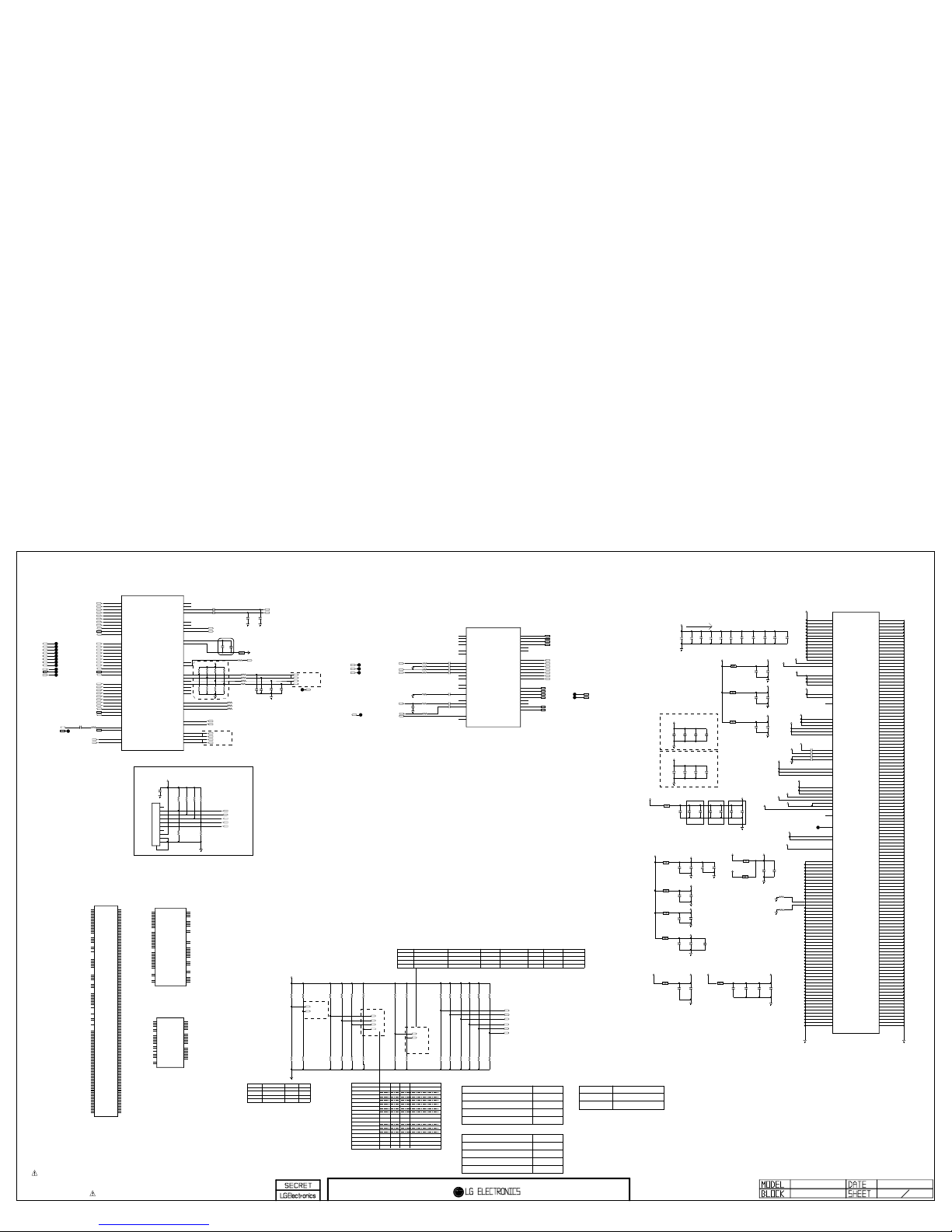
THE SYMBOL MARK OF THIS SCHEMETIC DIAGRAM INCORPORATES
SPECIAL FEATURES IMPORTANT FOR PROTECTION FROM X-RADIATION.
FIRE AND ELECTRICAL SHOCK HAZARDS, WHEN SERVICING IF IS
ESSENTIAL THAT ONLY MANUFACTURES SPECIFIED PARTS BE USED FOR
THE CRITICAL COMPONENTS IN THE SYMBOL MARK OF THE SCHEMETIC.
HP_LOUT_SOC
C356
0.1uF
16V
C343
0.1uF
16V
T2/S2
AUD_SCK
HDMI_HPD_5V_2
R341
4.7K
OPT
+3.3V_SB
R360
4.7K
OPT
C324
0.1uF
16V
CEC
TP300
C304
0.1uF
C360
0.1uF
16V
D_Demod_Core
C3140.047uF
D1+_HDMI3
BIT5
C371
0.1uF
JTAG
R361
4.7K
C348
0.1uF
16V
R316
4.7K
BIT5_0
CK-_HDMI2
C305
10uF
10V
AVDDL_DVI
R33333
R324
4.7K
Non_Brazil
CK-_HDMI3
R351
1K
OPT
R362
4.7K
OPT
BIT7
HDMI_ARC
W_VD33
COMP2_Pr+
R320
4.7K
BIT7_0
R300
4.7K
BIT0_1
R346
1K
JTAG
+3.3V_SB
VDD33
HDMI_HPD_5V_3
AVDDL_DVI
C333
0.1uF
16V
T2/S2
C3150.047uF
R317
4.7K
BIT6_1
D1+_HDMI1
VDD33
D0+_HDMI3
MODEL_OPT_8
AUD_LRCH
AVDDL_MOD
R33468
MODEL_OPT_9
MODEL_OPT_10
P300
12505WS-10A00
JTAG
1
2
3
4
5
6
7
8
9
10
11
R366
4.7K
OPT
C351
0.1uF
16V
C347
1uF
10V
R309
4.7K
BIT2_1
+3.3V_NORMAL
COMP2_Y+/AV_CVBS_IN
DTV/MNT_VOUT
MODEL_OPT_9
R348
1K
JTAG
R367
4.7K
OPT
C329
0.1uF
16V
BIT3
C361
0.1uF
16V
10uF
10V
C301
T2/S2
R33533
R312
4.7K
BIT3_0
DDC_SCL_3
TCK0
+3.3V_SB
C330
0.1uF
16V
C338
1uF
10V
D1-_HDMI1
C357
0.1uF
16V
W_VDD
C3160.047uF
BIT2
D0-_HDMI2
AVDD_3P3_USB
C350
0.1uF
16V
TP314
W_VDD
R33633
+3.3V_SB
TP310
AVDD_AU33
10uF
10V
C325
TCK0
W_VD33
C3170.047uF
MODEL_OPT_8
DDC_SDA_1
C342
0.1uF
16V
C359
0.1uF
16V
D2+_HDMI1
IC101
LGE6322(MSD93F2G, w/oT2S2 : M2)
EAN64207702
NON-MCP
A_RX0N
K2
A_RX0P
L3
A_RX1N
L2
A_RX1P
M3
A_RX2N
M2
A_RX2P
M1
A_RXCN
K3
A_RXCP
K1
DDCDA_CK
M5
DDCDA_DA
M6
HOTPLUGA
T4
B_RX0N
G2
B_RX0P
H3
B_RX1N
H2
B_RX1P
J3
B_RX2N
J2
B_RX2P
J1
B_RXCN
G3
B_RXCP
G1
DDCDB_CK
J4
DDCDB_DA
K4
HOTPLUGB
V4
D_RX0N
D2
D_RX0P
E3
D_RX1N
E2
D_RX1P
F3
D_RX2N
F2
D_RX2P
F1
D_RXCN
D3
D_RXCP
D1
DDCDD_CK
F4
DDCDD_DA
E4
HOTPLUGD
R4
ARC0
L5
CEC
G4
GPIO_PM[13]/MHL_CBUS
H5
GPIO_PM[14]/MHL_VBUS_EN
H6
LINEIN_L1
V1
LINEIN_R1
V3
LINEIN_L2
W1
LINEIN_R2
W2
LINEOUT_L0
T1
LINEOUT_R0
U3
LINEOUT_L2
W3
LINEOUT_R2
Y3
VAG
V2
AVSS_VRM_ADC
U2
SPDIF_IN
E21
SPDIF_OUT
D21
I2S_OUT_BCK
C26
I2S_OUT_MCK
D25
I2S_OUT_WS
C25
I2S_OUT_SD
D26
I2S_OUT_SD1/SDAM5
D24
I2S_OUT_SD2/SCKM5
E25
I2S_OUT_SD3(GPIO)
E24
I2S_IN_BCK
F22
I2S_IN_SD
E23
I2S_IN_WS
F23
DDCDC_CK(GPIO_PM)
AA2
DDCDC_DA(GPIO_PM)
AA3
GPIO2/EJ_TCK
B20
GPIO3/EJ_TMS
D22
GPIO4/EJ_TDI
D20
GPIO5/EJ_TDO
D23
COMP2_Pb+
MODEL_OPT_11
MODEL_OPT_10
C377
0.1uF
16V
C332
0.1uF
16V
10uF
10V
C323
R321
4.7K
OPT
IC101
LGE6322(MSD93F2G, w/oT2S2 : M2)
NON-MCP
RIN0P
P3
GIN0M
N2
GIN0P
N1
BIN0P
N3
HSYNC0
P5
VSYNC0
N6
RIN1P
R1
GIN1M
R2
GIN1P
R3
BIN1P
P2
HSYNC1
U5
VSYNC1
U6
NC_18
W4
NC_19
T2
VCOM
W6
CVBS0
W5
CVBS1
Y6
CVBS2
V5
CVBS_OUT1
V6
NC_20
Y5
TN
A5
TP
B5
RN
B6
RP
A6
GPIO19(LAN_LED[0])/ET_COL
C22
GPIO20(LAN_LED[1])/ET_TX_TXD1
B21
GPIO21/ET_TXD0
A21
GPIO22/ET_TX_EN
C20
GPIO23/ET_TX_CLK
C21
GPIO24/ET_RXD0
B22
GPIO25/ET_MDC
B23
GPIO26/ET_MDIO
C23
GPIO27/ET_RXD1
A22
DM_P0
P6
DP_P0
N5
DM_P1
R5
DP_P1
R6
DM_P2
A24
DP_P2
B24
DM_P3
T6
DP_P3
T5
DTV/MNT_VOUT
R310
4.7K
BIT2_0
C376
0.1uF
16V
C355
0.1uF
16V
R313
4.7K
BIT4_0
IC101
LGE6322(MSD93F2G, w/oT2S2 : M2)
NON-MCP
VDDC_1
G26
VDDC_2
H19
VDDC_3
J20
VDDC_4
J17
VDDC_5
J18
VDDC_6
J19
VDDC_7
K20
VDDC_8
K17
VDDC_9
K18
VDDC_10
K19
VDDC_11
L20
VDDC_12
L17
VDDC_13
L18
VDDC_14
L19
AVDDL_MOD
N18
AVDDL_DVI
T18
DVDD_DDR_A_1
R14
DVDD_DDR_A_2
R15
DVDD_DDR_B_1
H12
DVDD_DDR_B_2
J12
VDDC_SRAM_1
H17
VDDC_SRAM_2
H18
CTRL_SRAMLDO
H20
AVDD_DDR0_C
T14
AVDD_DDR0_D_1
T15
AVDD_DDR0_D_2
T16
AVDD_DDR1_C
J13
AVDD_DDR1_D_1
J14
AVDD_DDR1_D_2
J15
AVDD04_DDR_B
A8
AVDD04_DDR_A
AF7
AVDD11_DDR_B
B8
AVDD11_DDR_A
AE7
AVDD_PLL
G7
AVDD_MOD
L7
VDDP
H7
AVDD3P3_ETH
U7
AVDD3P3_ADC
P7
AVDD3P3_DADC
AB7
AVDD_AU33
T7
AVDD3P3_DMPLL
AA7
AVDD3P3_USB_1
N7
AVDD3P3_USB_2
N8
AVDD_NODIE
Y7
AVDD_5V_HDMI_D
D4
VSENSE_VDD
R20
NC_21
AB5
NC_22
AC5
VDDP_3318
Y18
GND_3
A11
GND_4
A14
GND_5
A17
GND_6
B7
GND_7
C6
GND_8
C7
GND_9
C8
GND_10
C9
GND_11
C19
GND_12
D14
GND_13
D17
GND_14
E9
GND_15
F9
GND_16
F10
GND_17
F11
GND_18
G6
GND_19
G8
GND_20
G9
GND_21
G10
GND_22
G11
GND_23
G12
GND_24
G13
GND_25
G14
GND_26
G15
GND_27
G16
GND_28
G17
GND_29
G18
GND_30
G19
GND_31
G20
GND_32
G21
GND_33
G22
GND_34
G23
GND_35
H9
GND_36
H10
GND_37
H11
GND_38
H13
GND_39
H14
GND_40
H15
GND_41
H16
GND_42
J8
GND_43
J9
GND_44
J10
GND_45
J11
GND_46
J16
GND_47
K7
GND_48
K8
GND_49
K9
GND_50
K10
GND_51
K11
GND_52
K12
GND_53
K13
GND_54
K14
GND_55
K15
GND_56
K16
GND_57
L8
GND_58
L9
GND_59
L10
GND_60
L11
GND_61
L12
GND_62
L13
GND_63
L14
GND_64
L15
GND_65
L16
GND_66
M8
GND_67
M9
GND_68
M10
GND_69
M12
GND_70
M13
GND_71
M14
GND_72
M15
GND_73
M16
GND_74
M17
GND_75
M18
GND_76
M19
GND_77
M20
GND_78
M21
GND_79
N9
GND_80
N12
GND_81
N13
GND_82
N14
GND_83
N15
GND_84
N16
GND_85
N17
GND_86
N19
GND_87
N20
GND_88
P8
GND_89
P9
GND_90
P12
GND_91
P13
GND_92
P14
GND_93
P15
GND_94
P16
GND_95
P17
GND_96
P18
GND_97
P19
GND_98
P20
GND_99
R7
GND_100
R8
GND_101
R9
GND_102
R12
GND_103
R13
GND_104
R16
GND_105
R17
GND_106
R18
GND_107
R19
GND_108
T3
GND_109
T8
GND_110
T9
GND_111
T10
GND_112
T11
GND_113
T12
GND_114
T13
GND_115
T17
GND_116
T19
GND_117
T20
GND_118
U8
GND_119
U9
GND_120
U10
GND_121
U11
GND_122
U12
GND_123
U13
GND_124
U14
GND_125
U15
GND_126
U16
GND_127
U17
GND_128
U18
GND_129
U19
GND_130
U20
GND_131
V7
GND_132
V8
GND_133
V9
GND_134
V10
GND_135
V11
GND_136
V12
GND_137
V13
GND_138
V14
GND_139
V15
GND_140
V16
GND_141
V17
GND_142
V18
GND_143
V19
GND_144
V20
GND_145
W7
GND_146
W8
GND_147
W9
GND_148
W10
GND_149
W11
GND_150
W12
GND_151
W13
GND_152
W14
GND_153
W15
GND_154
W16
GND_155
W17
GND_156
W18
GND_157
Y8
GND_158
Y9
GND_159
Y10
GND_160
Y11
GND_161
Y12
GND_162
Y13
GND_163
Y14
GND_164
Y15
GND_165
Y16
GND_166
Y17
GND_167
AA4
GND_168
AA5
GND_169
AA6
GND_170
AA8
GND_171
AA9
GND_172
AA13
GND_173
AB1
GND_174
AC7
GND_175
AC10
GND_176
AC13
GND_177
AC16
GND_178
AD6
GND_179
AD7
GND_180
AD17
GND_181
AD18
GND_182
AD22
GND_183
AD24
GND_184
AE2
GND_185
AE6
GND_186
AF10
GND_187
AF13
GND_188
AF16
R340 33
TP312
AVDD_3P3_USB
C340
0.1uF
16V
+1.10V_VDDC
R315
4.7K
BIT5_1
R337 68
D0-_HDMI3
C367 0.22uF
AVDD_DMPLL
10uF
10V
C322
D0-_HDMI1
C318 0.047uF
R314
4.7K
BIT4_1
C366 0.22uF
DDC_SCL_1
C321 0.047uF
BIT0
C368 0.22uF
R319
4.7K
BIT7_1
USB_DM2
R326
4.7K
INT_EEPROM
C369 0.22uF
AVDD_3P3
AVDD_3P3
DDC_SDA_2
USB_DP2
TDO0
R318
4.7K
BIT6_0
AVDD_DMPLL
C327
0.1uF
16V
HDMI_HPD_5V_1
WIFI_DM
TDI0
SPDIF_OUT
R307
0
OPT
AVDD_AU33
C354
0.1uF
16V
R304
4.7K
BIT1_1
USB_DP1
TMS0
DDC_SCL_2
R303
0
OPT
VDDP_NAND
C337
0.1uF
16V
R323
4.7K
Brazil
USB_DM1
SOC_RESET
MODEL_OPT_11
TP342
+3.3V_SB
C310
0.1uF
16V
R344
4.7K
DDR_LH60/DDR_LH57_1GB
WIFI_DP
R354
1K
OPT
D2-_HDMI3
+1.5V_DDR_1
3.3V_EMMC
C331
0.1uF
16V
C309
0.1uF
16V
D1+_HDMI2
EPHY_RDP
R353
0
OPT
R322
4.7K
DDR_1GB/512MB
+1.5V_DDR_1
DVDD18_EMMC
+1.5V_DDR_0
R343
4.7K
DDR_LH57_512MB
EPHY_RDN
R352
0
OPT
CK+_HDMI1
C319
0.1uF
16V
VDDP_NAND
C320
0.1uF
16V
D2+_HDMI3
EPHY_TDP
R350
1K
JTAG
BIT2
C334
0.1uF
16V
C341
0.1uF
16V
R327
4.7K
OPT
EPHY_TDN
R347
47K
OPT
BIT3
+1.5V_DDR_1
C339
0.1uF
16V
10uF
10V
C311
COMP2_Pb+
R305
4.7K
BIT1_0
10uF
10V
C364
+1.10V_VDDC
C313
0.1uF
16V
BIT6
COMP2_Y+/AV_CVBS_IN
R356 100
D0+_HDMI1
10uF
10V
C312
C365
0.1uF
16V
+1.10V_VDDC
TU_CVBS
BIT4
COMP2_Pr+
C372
22pF
OPT
DDC_SDA_3
10uF
10V
C328
R308 33
HP_DET
MODEL_OPT_12
R357 100
D0+_HDMI2
C3032.2uF
C353
0.1uF
16V
C336 0.047uF
CK+_HDMI2
MODEL_OPT_13
C373
22pF
OPT
BIT1
COMP2_L_IN
C363
0.1uF
16V
C344
0.1uF
16V
CK-_HDMI1
R358 100
D1-_HDMI2
COMP2_R_IN
C345
1000pF
OPT
TP313
D1-_HDMI3
C374
33pF
OPT
MODEL_OPT_13
C3022.2uF
AVDDL_MOD
R342
4.7K
BIT0
COMP2_Y+/AV_CVBS_IN
R359 100
TDI0
C362
0.1uF
16V
D2-_HDMI2
MODEL_OPT_12
C370
1uF
25V
C375
22pF
OPT
DVDD_DDR
R325
4.7K
EXT_EEPROM
C358
0.1uF
16V
C306
0.1uF
16V
T2/S2
D2-_HDMI1
R345
0
DVDD_DDR
C308
1000pF
50V
32inch_NON_EU
C326
0.1uF
16V
T2/S2
R311
4.7K
BIT3_1
R301
4.7K
BIT0_0
AUD_MASTER_CLK
R363
4.7K
+1.5V_DDR_0
D2+_HDMI2
C307
1000pF
50V
32inch_NON_EU
+1.10V_VDDC
AUD_LRCK
CEC
CK+_HDMI3
TP380
R364
4.7K
OPT
TDO0
HP_ROUT_SOC
C335
0.1uF
16V
T2/S2
AUD_MASTER_CLK
R328
4.7K
BIT1
R349
1K
JTAG
R365
4.7K
+1.5V_DDR_0
TMS0
TP320
D0-_HDMI2
TP321
D0+_HDMI2
TP322
D1-_HDMI2
TP323
D1+_HDMI2
TP324
D2-_HDMI2
TP325
D2+_HDMI2
TP326
CK-_HDMI2
TP327
CK+_HDMI2
TP328
TP329
TP330
DDC_SCL_2
HDMI_HPD_5V_2
DDC_SDA_2
USB_DM2
TP331
USB_DP2
TP332
C346
0.1uF
16V
L300
BLM15PX121SN1
L301
BLM15PX121SN1
L302
BLM15PX121SN1
T2/S2
L303
BLM15PX121SN1
L304
BLM15PX121SN1
T2/S2
L306
BLM15PX121SN1
L307
BLM15PX121SN1
L309
BLM15PX121SN1
L310
BLM15PX121SN1
L311
BLM15PX121SN1
L312
BLM15PX121SN1
L313
BLM15PX121SN1
OPT
L314
BLM15PX121SN1
IC101-*1
LGE6321(MSD93F2GW, w/ T2S2 : M2)
MCP
VDDC_1
G26
VDDC_2
H19
VDDC_3
J20
VDDC_4
J17
VDDC_5
J18
VDDC_6
J19
VDDC_7
K20
VDDC_8
K17
VDDC_9
K18
VDDC_10
K19
VDDC_11
L20
VDDC_12
L17
VDDC_13
L18
VDDC_14
L19
AVDDL_MOD
N18
AVDDL_DVI
T18
DVDD_DDR_A_1
R14
DVDD_DDR_A_2
R15
DVDD_DDR_B_1
H12
DVDD_DDR_B_2
J12
VDDC_SRAM_1
H17
VDDC_SRAM_2
H18
CTRL_SRAMLDO
H20
AVDD_DDR0_C
T14
AVDD_DDR0_D_1
T15
AVDD_DDR0_D_2
T16
AVDD_DDR1_C
J13
AVDD_DDR1_D_1
J14
AVDD_DDR1_D_2
J15
AVDD04_DDR_B
A8
AVDD04_DDR_A
AF7
AVDD11_DDR_B
B8
AVDD11_DDR_A
AE7
AVDD_PLL
G7
AVDD_MOD
L7
VDDP
H7
AVDD3P3_ETH
U7
AVDD3P3_ADC
P7
AVDD3P3_DADC
AB7
AVDD_AU33
T7
AVDD3P3_DMPLL
AA7
AVDD3P3_USB_1
N7
AVDD3P3_USB_2
N8
AVDD_NODIE
Y7
AVDD_5V_HDMI_D
D4
VSENSE_VDD
R20
NC_21
AB5
NC_22
AC5
VDDP_3318
Y18
GND_3
A11
GND_4
A14
GND_5
A17
GND_6
B7
GND_7
C6
GND_8
C7
GND_9
C8
GND_10
C9
GND_11
C19
GND_12
D14
GND_13
D17
GND_14
E9
GND_15
F9
GND_16
F10
GND_17
F11
GND_18
G6
GND_19
G8
GND_20
G9
GND_21
G10
GND_22
G11
GND_23
G12
GND_24
G13
GND_25
G14
GND_26
G15
GND_27
G16
GND_28
G17
GND_29
G18
GND_30
G19
GND_31
G20
GND_32
G21
GND_33
G22
GND_34
G23
GND_35
H9
GND_36
H10
GND_37
H11
GND_38
H13
GND_39
H14
GND_40
H15
GND_41
H16
GND_42
J8
GND_43
J9
GND_44
J10
GND_45
J11
GND_46
J16
GND_47
K7
GND_48
K8
GND_49
K9
GND_50
K10
GND_51
K11
GND_52
K12
GND_53
K13
GND_54
K14
GND_55
K15
GND_56
K16
GND_57
L8
GND_58
L9
GND_59
L10
GND_60
L11
GND_61
L12
GND_62
L13
GND_63
L14
GND_64
L15
GND_65
L16
GND_66
M8
GND_67
M9
GND_68
M10
GND_69
M12
GND_70
M13
GND_71
M14
GND_72
M15
GND_73
M16
GND_74
M17
GND_75
M18
GND_76
M19
GND_77
M20
GND_78
M21
GND_79
N9
GND_80
N12
GND_81
N13
GND_82
N14
GND_83
N15
GND_84
N16
GND_85
N17
GND_86
N19
GND_87
N20
GND_88
P8
GND_89
P9
GND_90
P12
GND_91
P13
GND_92
P14
GND_93
P15
GND_94
P16
GND_95
P17
GND_96
P18
GND_97
P19
GND_98
P20
GND_99
R7
GND_100
R8
GND_101
R9
GND_102
R12
GND_103
R13
GND_104
R16
GND_105
R17
GND_106
R18
GND_107
R19
GND_108
T3
GND_109
T8
GND_110
T9
GND_111
T10
GND_112
T11
GND_113
T12
GND_114
T13
GND_115
T17
GND_116
T19
GND_117
T20
GND_118
U8
GND_119
U9
GND_120
U10
GND_121
U11
GND_122
U12
GND_123
U13
GND_124
U14
GND_125
U15
GND_126
U16
GND_127
U17
GND_128
U18
GND_129
U19
GND_130
U20
GND_131
V7
GND_132
V8
GND_133
V9
GND_134
V10
GND_135
V11
GND_136
V12
GND_137
V13
GND_138
V14
GND_139
V15
GND_140
V16
GND_141
V17
GND_142
V18
GND_143
V19
GND_144
V20
GND_145
W7
GND_146
W8
GND_147
W9
GND_148
W10
GND_149
W11
GND_150
W12
GND_151
W13
GND_152
W14
GND_153
W15
GND_154
W16
GND_155
W17
GND_156
W18
GND_157
Y8
GND_158
Y9
GND_159
Y10
GND_160
Y11
GND_161
Y12
GND_162
Y13
GND_163
Y14
GND_164
Y15
GND_165
Y16
GND_166
Y17
GND_167
AA4
GND_168
AA5
GND_169
AA6
GND_170
AA8
GND_171
AA9
GND_172
AA13
GND_173
AB1
GND_174
AC7
GND_175
AC10
GND_176
AC13
GND_177
AC16
GND_178
AD6
GND_179
AD7
GND_180
AD17
GND_181
AD18
GND_182
AD22
GND_183
AD24
GND_184
AE2
GND_185
AE6
GND_186
AF10
GND_187
AF13
GND_188
AF16
IC101-*1
LGE6321(MSD93F2GW, w/ T2S2 : M2)
MCP
A_RX0N
K2
A_RX0P
L3
A_RX1N
L2
A_RX1P
M3
A_RX2N
M2
A_RX2P
M1
A_RXCN
K3
A_RXCP
K1
DDCDA_CK
M5
DDCDA_DA
M6
HOTPLUGA
T4
B_RX0N
G2
B_RX0P
H3
B_RX1N
H2
B_RX1P
J3
B_RX2N
J2
B_RX2P
J1
B_RXCN
G3
B_RXCP
G1
DDCDB_CK
J4
DDCDB_DA
K4
HOTPLUGB
V4
D_RX0N
D2
D_RX0P
E3
D_RX1N
E2
D_RX1P
F3
D_RX2N
F2
D_RX2P
F1
D_RXCN
D3
D_RXCP
D1
DDCDD_CK
F4
DDCDD_DA
E4
HOTPLUGD
R4
ARC0
L5
CEC
G4
GPIO_PM[13]/MHL_CBUS
H5
GPIO_PM[14]/MHL_VBUS_EN
H6
LINEIN_L1
V1
LINEIN_R1
V3
LINEIN_L2
W1
LINEIN_R2
W2
LINEOUT_L0
T1
LINEOUT_R0
U3
LINEOUT_L2
W3
LINEOUT_R2
Y3
VAG
V2
AVSS_VRM_ADC
U2
SPDIF_IN
E21
SPDIF_OUT
D21
I2S_OUT_BCK
C26
I2S_OUT_MCK
D25
I2S_OUT_WS
C25
I2S_OUT_SD
D26
I2S_OUT_SD1/SDAM5
D24
I2S_OUT_SD2/SCKM5
E25
I2S_OUT_SD3(GPIO)
E24
I2S_IN_BCK
F22
I2S_IN_SD
E23
I2S_IN_WS
F23
DDCDC_CK(GPIO_PM)
AA2
DDCDC_DA(GPIO_PM)
AA3
GPIO2/EJ_TCK
B20
GPIO3/EJ_TMS
D22
GPIO4/EJ_TDI
D20
GPIO5/EJ_TDO
D23
IC101-*1
LGE6321(MSD93F2GW, w/ T2S2 : M2)
MCP
RIN0P
P3
GIN0M
N2
GIN0P
N1
BIN0P
N3
HSYNC0
P5
VSYNC0
N6
RIN1P
R1
GIN1M
R2
GIN1P
R3
BIN1P
P2
HSYNC1
U5
VSYNC1
U6
NC_18
W4
NC_19
T2
VCOM
W6
CVBS0
W5
CVBS1
Y6
CVBS2
V5
CVBS_OUT1
V6
NC_20
Y5
TN
A5
TP
B5
RN
B6
RP
A6
GPIO19(LAN_LED[0])/ET_COL
C22
GPIO20(LAN_LED[1])/ET_TX_TXD1
B21
GPIO21/ET_TXD0
A21
GPIO22/ET_TX_EN
C20
GPIO23/ET_TX_CLK
C21
GPIO24/ET_RXD0
B22
GPIO25/ET_MDC
B23
GPIO26/ET_MDIO
C23
GPIO27/ET_RXD1
A22
DM_P0
P6
DP_P0
N5
DM_P1
R5
DP_P1
R6
DM_P2
A24
DP_P2
B24
DM_P3
T6
DP_P3
T5
R355 100
3
2015.10.02
MAIN2
16Y_M2
0 / 1
768MB
1 / 1 / 1 / 1
1GB
LVDS FHD, 60Hz, CP BOX
-
BRAZIL
-
1 / 1
DDR
EPI FHD, 120Hz, V12 (6 lane)
LH60 DDR OPTION
LVDS HD, 60Hz SMALL SMART
FRC
(T2/C/S2)_SOC/ATV_CVBS
KOREA
0 / 0 / 1 / 1
(T2/C)_SOC/ATV_IF
TUNER OPTION
BIT [0/1]
Model Option
ATSC_CVBS
1 / 1 / 0 / 1
T2/C/ATV_IF
0 / 0 / 0 / 0
LVDS FHD, 120Hz
1 / 0
ATSC_CVBS
0 / 0
1 / 1
T2/C/ATV_CVBS
DVB
(T/C)_SOC/ATV_CVBS
LVDS HD, 60Hz
CHINA/HONG
1 / 0 / 1 / 0
0 / 1 / 1 / 0
S/AMERCIA
JP
N/AMERICA
LVDS FHD, 60Hz
JAPAN
1 / 1 / 0 / 0
(T2/C)_SOC/ATV_CVBS
0 / 0 / 1 / 0
ASIA/AFRICA
EPI FHD, 60Hz, V14_32 inch (6lane)
EPI FHD, 120Hz, V13 (6 lane)
PANEL TYPE
LVDS FHD, 120Hz OLED
TAIWAN/COLOM
0 / 1 / 1 / 1
KOREA
1 / 1 / 1 / 0
CHINA/HONGKONG
ISDB/ATV_IF
VDDC 1.05V
ISDB/ATV_CVBS
0 / 1
0 / 0
STby 3.4V
(T2/C/S2)_EXT/ATV_CVBS
0 / 1 / 0 / 0
Normal Power 3.3V
FHD
Vby1 FHD, 120Hz
AVDD_PLL
OLED
EU/CIS
AVDD_MOD
AJJA
(T2/C/S2)_SOC/ATV_CVBS
VDDP
BACK-END OPTION
TAIWAN/COL
Closed to SoC Side
1 / 0
1 / 0 / 1 / 1
I2S_I/F
1 / 0 / 0 / 1
0 / 0 / 0 / 1
Jtag I/F
For Main
T/C/ATV_CVBS
NORTH AMERICA
JTAG
EPI FHD, 120Hz, v14_32inch (6 lane)
(T2/C)_SOC/ATV_CVBS
Chip config.
T/C/ATV_IF
1 / 0 / 0 / 0
DDR3 1.5V
0 / 1 / 0 / 1
EPI FHD, 120Hz, V14 (8 lane)
DDR3 1.5V
EU/CIS
AREA OPTION
MODEL_OPT_8 / MODEL_OPT_12
BIT[2/3/4/5]
BIT [6/7]
0 / 0
ATSC
(T2/C)_SOC/ATV_IF
1 / 0
TYPE
0 / 1
(DTMB)_EXT/ATV_CVBS
1 / 1
AREA OPTION
0 / 0
1 / 0
-
0 / 1
DDR
1 / 1
LH57 DDR OPTION
768MB
512MB
MODEL_OPT_8 / MODEL_OPT_13
1GB
Brazil
0
DDR Brazil OPT_LH60/LH57 COMMON
1
DDR Country OPT
MODEL_OPT_9
Non Brazil
Copyright © 2016 LG Electronics Inc. All rights reserved.
Only for training and service purposes
LGE Internal Use Only
 Loading...