

LG 47WV30BS-BL Schematic
Internal Use Only
North/Latin America http://aic.lgservice.com
Europe/Africa http://eic.lgservice.com
Asia/Oceania http://biz.lgservice.com
MONITOR SIGNAGE
SERVICE MANUAL
CHASSIS : LW01A
MODEL : 47WV30BS 47WV30BS-BL
CAUTION
BEFORE SERVICING THE CHASSIS,
READ THE SAFETY PRECAUTIONS IN THIS MANUAL.
Printed in KoreaP/NO : MFL63279926 (1112-REV00)

CONTENTS
CONTENTS .............................................................................................. 2
PRECAUTION
SERVICING PRECAUTIONS
SPECIFICATION
ADJUSTMENT INSTRUCTION
TROUBLE SHOOTING
BLOCK DIAGRAM
EXPLODED VIEW
........................................................................................... 3
.................................................................... 4
....................................................................................... 6
................................................................ 9
........................................................................... 15
.................................................................................. 22
.................................................................................. 23
SCHEMATIC CIRCUIT DIAGRAM
..............................................................
Only for training and service purposes
- 2 -
LGE Internal Use OnlyCopyright © LG Electronics. Inc. All rights reserved.

PRECAUTION
WARNING FOR THE SAFETY-RELATED COMPONENT.
• There are some special components used in LCD
zmonitor that are important for safety. These parts are
marked
Exploded View. It is essential that these critical parts
should be replaced with the manufacturer' s specified
parts to prevent electric shock, fire or other hazard.
• Do not modify original design without obtaining written
permission from manufacturer or you will void the
original parts and labor guarantee.
TAKE CARE DURING HANDLING THE LCD MODULE
WITH BACKLIGHT UNIT.
• Must mount the module using mounting holes arranged
in four corners.
• Do not press on the panel, edge of the frame strongly or
electric shock as this will result in damage to the
screen.
• Do not scratch or press on the panel with any sharp
objects, such as pencil or pen as this may result in
damage to the panel.
• Protect the module from the ESD as it may damage the
electronic circuit (C-MOS).
on th e schematic diagram and the
WARNING
BE CAREFUL ELECTRIC SHOCK !
• If you want to replace with the new backlight (CCFL) or
inverte r ci rcuit, must disconne ct the AC ada pter
because high voltage appears at inverter circuit about
650Vrms.
• Handle with care wires or connectors of the inverter
circuit. If the wires are pressed cause short and may
burn or take fire.
• Make certain that treatment person' s body are grounded
through wrist band.
• Do not leave the module in high temperature and in
areas of high humidity for a long time.
• The module not be exposed to the direct sunlight.
• Avoid contact with water as it may a short circuit within
the module.
• If the surface of panel become dirty, please wipe it off
with a softmaterial. (Cleaning with a dirty or rough cloth
may damage the panel.)
CAUTION
Please use only a plastic screwdriver to protect yourself
from shock hazard during service operation.
Leakage Current Hot Check Circuit
• Replaceable batteries
* CAUTION
RISK OF EXPLOSION IF BATTERY IS REPLACED BY
AN INCORRECT TYPE.
DISPOSE OF USED BATTERIES ACCORDING TO
THE INSTRUCTIONS.
REPLACE ONLY WITH THE SAME OR EQUIVALENT
TYPE.
Only for training and service purposes
- 3 -
LGE Internal Use OnlyCopyright © LG Electronics. Inc. All rights reserved.

SERVICING PRECAUTIONS
CAUTION: Before servicing receivers covered by this service
manual and its supplements and addenda, read and follow the
SAFETY PRECAUTIONS on page 3 of this publication.
NOTE: If unforeseen circumstances create conflict between the
following servicing precautions and any of the safety precautions on
page 3 of this publication, always follow the safety precautions.
Remember: Safety First.
General Servicing Precautions
1. Always unplug the receiver AC power cord from the AC power
source before;
a. Removing or reinstalling any component, circuit board
module or any other receiver assembly.
b. Disconnecting or reconnecting any receiver electrical plug or
other electrical connection.
c. Connecting a test substitute in parallel with an electrolytic
capacitor in the receiver.
CAUTION: A wrong part substitution or incorrect polarity
installation of electrolytic capacitors may result in an
explosion hazard.
2. Test high voltage only by measuring it with an appropriate high
voltage meter or other voltage measuring device (DVM,
FETVOM, etc) equipped with a suitable high voltage probe.
Do not test high voltage by "drawing an arc".
3. Do not spray chemicals on or near this receiver or any of its
assemblies.
4. Unl ess specified othe rwise in this service manua l, clean
electrical contacts only by applying the following mixture to the
contacts with a pipe cleaner, cotton-tipped stick or comparable
non-abrasive applicator; 10% (by volume) Acetone and 90% (by
volume) isopropyl alcohol (90%-99% strength)
CAUTION: This is a flammable mixture.
Unless specified otherwise in this service manual, lubrication of
contacts in not required.
5. Do not defeat any plug/socket B+ voltage interlocks with which
receivers covered by this service manual might be equipped.
6. Do not apply AC power to this instrument and/or any of its
electrical assemblies unless all solid-state device heat sinks are
correctly installed.
7. Always connect the test receiver ground lead to the receiver
chassis ground before connecting the test receiver positive
lead.
Always remove the test receiver ground lead last.
8. Use with this receiver only the test fixtures specified in this
service manual.
CAUTION: Do not connect the test fixture ground strap to any
heat sink in this receiver.
Electrostatically Sensitive (ES) Devices
Some semiconductor (solid-state) devices can be damaged easily
by static electricity. Such components com monly are called
Electrostatically Sensitive (ES) Devices. Examples of typical ES
devices are integrated circuits and some field-effect transistors and
semiconductor "chip" compon ents. The following techniques
should be used to help reduce the incide nce of component
damage caused by static by static electricity.
1. Immediately before handling any semiconductor component or
semiconductor-equipped assembly, drain off any electrostatic
charge on your body by touching a known earth ground.
Alter natively, obtain and wear a comme rcially availab le
discharging wrist strap device, which should be removed to
prevent potential shock reasons prior to applying power to the
unit under test.
2. After removing an electrical assembly equipped with ES
devices, place the assembly on a conductive surface such as
aluminum foil, to prevent electrostatic charge buildup or
exposure of the assembly.
3. Use only a grounded-tip soldering iron to solder or unsolder ES
devices.
4. Use only an anti-static type solder removal device. Some solder
removal devices not classified as "anti-static" can generate
electrical charges sufficient to damage ES devices.
5. Do not use freon-propelled chemicals. These can generate
electrical charges sufficient to damage ES devices.
6. Do not remove a replacement ES device from its protective
package until immediately before you are ready to install it.
(Most re pla cem ent ES dev ice s are packaged with leads
electrically shorted together by conductive foam, aluminum foil
or comparable conductive material).
7. Immediately before removing the protective material from the
leads of a replacement ES device, touch the protective material
to the chassis or circuit assembly into which the device will be
installed.
CAUTION: Be sure no power is applied to the chassis or circuit,
and observe all other safety precautions.
8. Mi nimiz e bodil y motions w hen h an dl ing u np ac kaged
replacement ES devices. (Otherwise harmless motion such as
the brushing together of your clothes fabric or the lifting of your
foot from a carp eted floor can ge ner ate st atic electricit y
sufficient to damage an ES device.)
General Soldering Guidelines
1. Use a grounded-tip, low-wattage soldering iron and appropriate
tip size and shape that will maintain tip temperature within the
range or 500 ˚F to 600 ˚F.
2. Use an appropriate gauge of RMA resin-core solder composed
of 60 parts tin/40 parts lead.
3. Keep the soldering iron tip clean and well tinned.
4. Thoroughly clean the surfaces to be soldered. Use a mall wirebristle (0.5 inch, or 1.25cm) brush with a metal handle.
Do not use freon-propelled spray-on cleaners.
5. Use the following unsoldering technique
a. Allow the soldering iron tip to reach normal temperature.
(500 ˚F to 600 ˚F)
b. Heat the component lead until the solder melts.
c. Quickly draw the melted solder with an anti-static, suction-
type solder removal device or with solder braid.
CAUTION: Work quickly to avoid overheating the circuit
board printed foil.
6. Use the following soldering technique.
a. Allow the soldering iron tip to reach a normal temperature
(500 ˚F to 600 ˚F)
b. First, hold the soldering iron tip and solder the strand against
the component lead until the solder melts.
c. Quickly move the soldering iron tip to the junction of the
component lead and the printed circuit foil, and hold it there
only un til the solder fl ows onto and around both the
component lead and the foil.
CAUTION: Work quickly to avoid overheating the circuit
board printed foil.
d. Closely inspect the solder area and remove any excess or
splashed solder with a small wire-bristle brush.
Only for training and service purposes
- 4 -
LGE Internal Use OnlyCopyright © LG Electronics. Inc. All rights reserved.

IC Remove/Replacement
Some chassis circuit boards have slotted holes (oblong) through
which the IC leads are inserted and then bent flat against the
circuit foil. When holes are the slotted type, the following technique
should be used to remove and replace the IC. When working with
boards using the familiar round hole, use the standard technique
as outlined in paragraphs 5 and 6 above.
Removal
1. Desolder and straighten each IC lead in one operation by gently
prying up on the lead with the soldering iron tip as the solder
melts.
2. Draw away the melted solder with an anti-static suction-type
solder removal device (or with solder braid) before removing the
IC.
Replacement
1. Carefully insert the replacement IC in the circuit board.
2. Carefully bend each IC lead against the circuit foil pad and
solder it.
3. Clean the soldered areas with a small wire-bristle brush.
(It is not necessary to reapply acrylic coating to the areas).
"Small-Signal" Discrete Transistor
Removal/Replacement
1. Remove the defective transistor by clipping its leads as close as
possible to the component body.
2. Bend into a "U" shape the end of each of three leads remaining
on the circuit board.
3. Bend into a "U" shape the replacement transistor leads.
4. Connect the replacement transistor leads to the corresponding
leads extending from the circuit board and crimp the "U" with
long nose pliers to insure metal to metal contact then solder
each connection.
CAUTION: Maintain original spacing between the replaced
component and adjacent components and the circuit board to
prevent excessive component temperatures.
Circuit Board Foil Repair
Excessive heat applied to the copper foil of any printed circuit
board will weaken the adhesive that bonds the foil to the circuit
board causing the foil to separate from or "lift-off" the board. The
following guidelines and procedures should be followed whenever
this condition is encountered.
At IC Connections
To repair a defective copper pattern at IC connections use the
following procedure to install a jumper wire on the copper pattern
si de of the circuit board. (Use this techniq ue onl y on IC
connections).
1. Carefully remove the damaged copper pattern with a sharp
knife. (Remove only as much copper as absolutely necessary).
2. carefully scratch away the solder resist and acrylic coating (if
used) from the end of the remaining copper pattern.
3. Bend a small "U" in one end of a small gauge jumper wire and
carefully crimp it around the IC pin. Solder the IC connection.
4. Route the jumper wire along the path of the out-away copper
pattern and let it overlap the previously scraped end of the good
copper pattern. Solder the overlapped area and clip off any
excess jumper wire.
At Other Connections
Use the following technique to repair the defective copper pattern
at connections other than IC Pins. This technique involves the
installation of a jumper wire on the component side of the circuit
board.
Power Output, Transistor Device
Removal/Replacement
1. Heat and remove all solder from around the transistor leads.
2. Remove the heat sink mounting screw (if so equipped).
3. Carefully remove the transistor from the heat sink of the circuit
board.
4. Insert new transistor in the circuit board.
5. Solder each transistor lead, and clip off excess lead.
6. Replace heat sink.
Diode Removal/Replacement
1. Remove defective diode by clipping its leads as close as
possible to diode body.
2. Bend the two remaining leads perpendicular y to the circuit
board.
3. Observing diode polarity, wrap each lead of the new diode
around the corresponding lead on the circuit board.
4. Securely crimp each connection and solder it.
5. Inspect (on the circuit board copper side) the solder joints of
the two "original" leads. If they are not shiny, reheat them and if
necessary, apply additional solder.
Fuse and Conventional Resistor
Removal/Replacement
1. Clip each fuse or resistor lead at top of the circuit board hollow
stake.
2. Securely crimp the leads of replacement component around
notch at stake top.
3. Solder the connections.
1. Remove the defective copper pattern with a sharp knife.
Remove at least 1/4 inch of copper, to ensure that a hazardous
condition will not exist if the jumper wire opens.
2. Trace along the copper pattern from both sides of the pattern
break an d loc ate the nearest component that is dir ect ly
connected to the affected copper pattern.
3. Connect insulated 20-gauge jumper wire from the lead of the
nearest component on one side of the pattern break to the lead
of the nearest component on the other side.
Carefully crimp and solder the connections.
CAUTION: Be sure the insulated jumper wire is dressed so the
it does not touch components or sharp edges.
Only for training and service purposes
- 5 -
LGE Internal Use OnlyCopyright © LG Electronics. Inc. All rights reserved.
SPECIFICATION
NOTE : Specifications and others are subject to change without notice for improvement
.
1. Application range
This specification is applied to the LW01A chassis.
2. Requirement for Test
Each part is tested as below without special appointment.
(1) Temperature: 25 °C ± 5 °C(77 °F ± 9 °F),
CST: 40 °C ± 5 °C
(2) Relative Humidity: 65 % ± 10 %
(3) Power Voltage
: Standard input voltage (AC 100-240 V~, 50/60 Hz)
* Standard Voltage of each products is marked by models.
(4) Specification and performance of each parts are followed
ea ch dra wing and speci ficat ion by part number in
accordance with BOM.
(5) The receiver must be operated for about 5 minutes prior to
the adjustment.
3. Test method
(1) Performance: LGE Monitor test method followed.
(2) Demanded other specification
- Safety : CE, IEC specification
- EMC : CE, IEC
4. Model General Specification
4.1. Module Specification
No Item Specication Remark
1 Display Screen Device 47” wide Color Display Module
2 Aspect Ratio 16 : 9
3 LCD Module 47” LED LCD HD 47” LGD, LED LCD (HD)
4 Storage Environment Temp. : -20 ~ 60 deg
Humidity : 10 ~ 90 %
5 Input Voltage AC 100 ~ 240V, 50/60Hz
6 Pixel Pitch 0.5415mm x 0.5415mm
7 Back Light Direct LED
8 Display Colors 16.7M (HD)
9 Coating 3H, AG
4.2. Model Specification
No Item Specication Remark
1 Market WORLD WIDE
2 Component In (1EA) Y/Cb/Cr
Y/Pb/Pr
3 HDMI In(EA) HDMI-DTV/DVI PC(HDMI version 1.3)
Support HDCP
4 RGB In/Out (1EA) RGB In/Out
5 DVI In/Out (1EA) Digital In/Out Input : Support HDCP
Output : Not support HDCP
6 RS 232C In/Out (1EA) RS 232C In/Out
7 Audio In (2EA) RGB/DVI Audio
Component Audio
8 RJ45 Ethernet WOL, NSU(Network Software Update)
9 USB DivX, JPEG, MP3, SVC(download)
10 Ext. IR (1EA) IR Receiver
11 Ext. Speaker Out (1EA) Ext. Speaker Out
Only for training and service purposes
L/R Input
- 6 -
LGE Internal Use OnlyCopyright © LG Electronics. Inc. All rights reserved.
5. Component Video Input (Y, P
No.
Resolution H-freq(kHz) V-freq(Hz) Proposed
1 720×480 15.73 60.00 SDTV, DVD 480i
2 720×480 15.63 59.94 SDTV, DVD 480i
3 720×480 31.47 59.94 480p
4 720×480 31.50 60.00 480p
5 720×576 15.625 50.00 SDTV, DVD 625 Line
6 720×576 31.25 50.00 HDTV 576p
7 1280×720 45.00 50.00 HDTV 720p
8 1280×720 44.96 59.94 HDTV 720p
9 1280×720 45.00 60.00 HDTV 720p
10 1920×1080 31.25 50.00 HDTV 1080i
11 1920×1080 33.75 60.00 HDTV 1080i
12 1920×1080 33.72 59.94 HDTV 1080i
, PR)
B
Specication Remark
6. RGB Input ( PC Only )
No Resolution H-freq(kHz) V-freq.(Hz) Pixel clock (MHz) Proposed Remarks
1 720*400 31.468 70.08 28.321 For only DOS mode
2 640*480 31.469 59.94 25.17 VESA
3 800*600 37.879 60.31 40.00 VESA
4 832*624 49.725 74.55 55.00 MAC
5 1024*768 48.363 60.00 65.00 VESA(XGA)
6 1280*720 45.00 60.00 74.25 VESA
7 1360*768 47.72 59.8 84.75 WXGA
8 1366*768 47.71 59.79 85.50 WXGA
9 1280*1024 63.595 60.0 108.875 SXGA
Only for training and service purposes
- 7 -
LGE Internal Use OnlyCopyright © LG Electronics. Inc. All rights reserved.
7. HDMI(PC/DTV) / DVI(PC Mode Only) input
7.1. PC mode
No Resolution H-freq(kHz) V-freq.(Hz) Pixel clock(MHz) Proposed Remarks
1 720*400 31.468 70.08 28.321 For only DOS mode
2 640*480 31.469 59.94 25.17 VESA
3 800*600 37.879 60.31 40.00 VESA
4 1024*768 48.363 60.00 65.00 VESA(XGA)
5 1280*720 45.00 60.00 74.25 VESA
6 1360*768 47.72 59.8 84.75 WXGA
7 1366*768 47.71 59.79 85.50 WXGA
8 1280*1024 63.595 60.0 108.875 SXGA
7.2. DTV mode
No Resolution H-freq(kHz) V-freq.(kHz) Pixel clock(MHz) Proposed Remarks
1 720*480 31.469 / 31.5 59.94 / 60 27.00/27.03 SDTV 480P HDCP
2 720*576 31.25 50 54 SDTV 576P HDCP
3 1280*720 37.500 50 74.25 HDTV 720P HDCP
4 1280*720 44.96 / 45 59.94 / 60 74.17/74.25 HDTV 720P HDCP
5 1920*1080 33.72 / 33.75 59.94 / 60 74.17/74.25 HDTV 1080I HDCP
6 1920*1080 28.125 50.00 74.25 HDTV 1080I HDCP
Only for training and service purposes
- 8 -
LGE Internal Use OnlyCopyright © LG Electronics. Inc. All rights reserved.

ADJUSTMENT INSTRUCTION
1. Application Range
This specification is applied all of the Digital Signage Product
with LW01A chassis.
2. Designation
(1) Th e ad justm ent is accord ing to the order whic h is
designated and which must be followed, according to the
plan which can be changed only on agreeing.
(2) Power adjustment : Free Voltage.
(3) Magnetic Field Condition: Nil.
(4) Input signal Unit: Product Specification Standard.
(5) Reserve after operation: Above 5 Minutes (Heat Run)
Temperature : at 25 °C ± 5 °C
Relative humidity : 65 % ± 10 %
Input voltage : 220V, 60Hz
(6) Adjustment equipments : Color Analyz er (CA-210 or
CA-110), DDC Adjustment Jig equipment, SVC remote
controller.
(7) Push The “IN STOP KEY” – For memory initialization.
Case1 : Software version up
1. After downloading S/W by USB , Multi-vision set will reboot
automatically
2. Push “In-stop” key
3. Push “Power on” key
4. Function inspection
5. After function inspection, Push “In-stop” key.
Case2 : Function check at the assembly line
1. When TV set is entering on the assembly line, Push “Instop” ke y at rst.
2. Push “Power on” key for turning it on.
-> If you push “Power on” key, TV set will recover channel
information by itself.
3. After function inspection, Push “In-stop” key.
(4) Click “Connect” tab. If “Can’t ” is displayed, Check
connection between computer, jig, and set.
(5) Click “Auto” tab and set as below.
(6) Click "Run".
(7) After downloading, check "OK" message.
* USB DOWNLOAD(*.epk file download)
(1) Put the USB Stick to the USB socket
(2) Automatically detecting update file in USB Stick
- If your downloaded program version in USB Stick is Low,
it didn’t work.
- Bu t your downloaded version is High, USB data is
automatically detecting
(3) Show the message “Copying files from memory”
3. Main PCB check process
* APC - After Manual-Insult, executing APC
* Boot file Download
(1) Execute ISP program “Mstar ISP Utility” and then click
“Config” tab.
(2) Set as below, and then click “Auto Detect” and check “OK”
message
If “Error” is displayed, Check connection between computer,
jig, and set.
(3) Click “Read” tab, and then load download file (XXXX.bin)
by clicking “Read”
Only for training and service purposes
(4) Updating is staring.
(5) Updating C om pl et ed , T he Multi-vi si on will r es ta rt
automatically.
(6) If your Multi-vision is turned on, check your updated
version and Tool option. (explain the Tool option, next
stage)
- 9 -
LGE Internal Use OnlyCopyright © LG Electronics. Inc. All rights reserved.
* After downloading, have to adjust TOOL OPTION again.
1) Push "IN-START" key in service remote controller.
2) Select "Tool Option 1" and Push “OK” button.
3) Punch in the number. (Each of mode ls has their
number.)
Model 47WV30BS-BL
Module LGD
Global
EU sufx Exception for EU
Tool Option 1 33760 33760
Tool Option 2 8707 8707
Tool Option 3 49172 51220
Tool Option 4 29056 29056
Tool Option 5 1056 1056
Global
Exception for
US & Korea
Tool Option 1 33760 33760
Tool Option 2 8707 8707
Tool Option 3 49172 51220
Tool Option 4 29056 29056
Tool Option 5 1056 1056
4) Completed selecting Tool option.
US & Korea
sufx
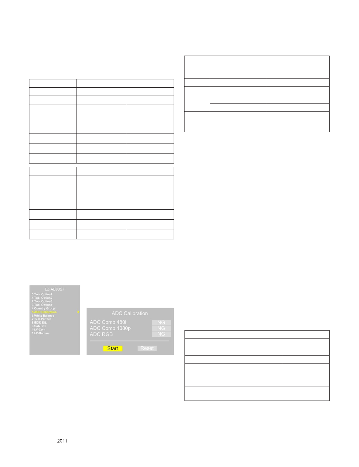
* ADC Calibration Protocol (RS232)
NO Enter
Adjust MODE
Item Adjust ‘Mode In’ ADC Adjust
CMD 1 A A
CMD 2 A D
Data 0 0 0
1 0
When transfer the
‘Mode In’,
Carry the command.
- Adjust Sequence
▪aa 00 00 [Enter Adjust Mode]
▪xb 00 40 [Component1 Input (480i)]
▪ad 00 10 [Adjust 480i Comp1]
▪xb 00 60 [RGB Input (1024*768)]
▪ad 00 10 [Adjust 1024*768 RGB]
▪aa 00 90 End Adjust mode
* Required equipment : Adjustment R/C.
ADC adjust
Automatically adjustment
(The use of a internal
pattern)
3.2. Function Check
3.2.1. Check display and sound
■ Check Input and Signal items. (cf. work instructions)
1. COMPONENT (480i)
2. RGB (PC : 1024 x 768 @ 60hz)
3. HDMI
4. DVI
5. PC Audio In
* Display and Sound check is executed by Remote control-
ler.
3.1. ADC Process
3.1.1. ADC
■ Enter Service Mode by pushing “ADJ” key,
■ Enter Internal ADC mode by pushing “►” key at “5. ADC
Calibration”
* Caution : Using ‘power on’ button of the Adjustment R/C,
power on Multi-vision.
* Caution : Not to push the INSTOP KEY after completion if the
function inspection.
4. Total Assembly line process
4.1. Adjustment Preparation
■ W/B Equipment condition
CA210 : CH 9, Test signal : Inner pattern (85IRE)
■ Above 5 minutes H/run in the inner pattern. (“power on” key
of adjust remote control)
Color Temperature
Cool Medium Warm
13,000k 9,300k 6,500k
K K K
X=0.269 (±0.002)
Y=0.273 (±0.002)
X=0.285 (±0.002)
Y=0.293 (±0.002)
47WV30
<Test Signal>
Inner pattern (216gray,85IRE)
X=0.313 (±0.002)
Y=0.329 (±0.002)
Only for training and service purposes
- 10 -
LGE Internal Use OnlyCopyright © LG Electronics. Inc. All rights reserved.

* Connecting picture of the measuring instrument (On Auto-
matic control)
- Inside PATTERN is used when W/B is controlled. Connect to auto controller or push Adjustment R/C POWERON -> Enter the mode of White-Balance, the pattern will
come out.
* Auto-control interface and directions
1) Adjust in the place where the inux of light like oodlight
around is blocked. (Illumination is less than 100Lux).
2) Adhere closely the Color Analyzer ( CA210 ) to the
module less than 10cm distance, keep it with the surface
of the Module and Color Analyzer’s Prove vertically.
(80~100°).
3) Aging time
- After aging start, keep the power on (no suspension of
power supply) and heat-run over 5 minutes.
- Using ‘no signal’ or ‘full white pattern’ or the others,
check the back light on.
* After You nish all adjustments, Press “In-start” button and
compare Tool option and Area option value with its BOM, if it
is correctly same then unplug the AC cable.
If it is not same, then correct it same with BOM and unplug
AC cable.
For correct it to the model’s module from factory JIG model.
* Push The “IN STOP KEY” after completing the function
inspection. And Mechanical Power Switch must be set “ON”.
4.2. MAC Address Download
■ Auto adjustment Map(RS-232C)
RS-232C COMMAND
[ CMD ID DATA ]
Wb 00 00 White Balance Start
Wb 00 ff White Balance End
RS-232C
COMMAND
[CMD ID DATA]
Cool Mid Warm Cool Mid Warm
R Gain jg Ja jd 00 172 192 192 192
G Gain jh Jb je 00 172 192 192 192
B Gain ji Jc jf 00 192 192 172 192
R Cut 64 64 64 128
G Cut 64 64 64 128
B Cut 64 64 64 128
*Caution
- Color Temperature : COOL, Medium, Warm.
- One of R Gain/G Gain/ B Gain should be kept on 0xC0, and
adjust other two lower than C0.
( when R/G/B Gain are all C0, it is the FULL Dynamic Range
of Module)
* Manual W/B process using adjusts Remote control.
■ After enter Service Mode by pushing “ADJ” key,
■ Enter White Balance by pushing “►” key at “6. White
Balance”.
M
I
N
CENTER
(DEFAULT)
M
A
X
■ Com 1,2,3,4 and 115200(Baudrate)
■ Port connection button click(1)
■ Load button click(2) for MAC Address write.
■ Start MAC Address write button(3)
■ Check the OK Or NG
4.3. LAN (Automatic IP)
4.3.1. Equipment & Condition
■ Each other connection to LAN Port of IP Hub and Jig
4.3.2. LAN inspection solution
■LAN Port connection with PCB
■ Network setting at MENU Mode of Menu
- “menu” key input -> Network -> Network Setting ->
Press “Enter” -> IP Auto Setting -> OK
■ setting automatic IP
■ Setting state conrmation
- If automatic setting is nished, you conrm IP and
MAC Address.
Only for training and service purposes
- 11 -
LGE Internal Use OnlyCopyright © LG Electronics. Inc. All rights reserved.
 Loading...