

Page 1

LCD TV
SERVICE MANUAL
CAUTION
BEFORE SERVICING THE CHASSIS,
READ THE SAFETY PRECAUTIONS IN THIS MANUAL.
CHASSIS : LP7AB
MODEL : 47LB9R
47LB9R-TD
website:http://biz.LGservice.com
Internal Use Only
Page 2

Copyright © 2007 LG Electronics. Inc. All right reserved.
Only for training and service purposes
LGE Internal Use Only
- 2 -
CONTENTS
CONTENTS .............................................................................................. 2
PRODUCT SAFETY ..................................................................................3
SPECIFICATION ........................................................................................6
ADJUSTMENT INSTRUCTION ...............................................................10
TROUBLE SHOOTING ............................................................................15
BLOCK DIAGRAM...................................................................................20
EXPLODED VIEW .................................................................................. 21
REPLACEMENT PARTS LIST ............................................................... 23
SVC. SHEET ...............................................................................................
Page 3

Copyright © 2007 LG Electronics. Inc. All right reserved.
Only for training and service purposes
LGE Internal Use Only
- 3 -
SAFETY PRECAUTIONS
Many electrical and mechanical parts in this chassis have special safety-related characteristics. These parts are identified by in the
Schematic Diagram and Replacement Parts List.
It is essential that these special safety parts should be replaced with the same components as recommended in this manual to prevent
Shock, Fire, or other Hazards.
Do not modify the original design without permission of manufacturer.
General Guidance
An isolation Transformer should always be used during the
servicing of a receiver whose chassis is not isolated from the AC
power line. Use a transformer of adequate power rating as this
protects the technician from accidents resulting in personal injury
from electrical shocks.
It will also protect the receiver and it's components from being
damaged by accidental shorts of the circuitry that may be
inadvertently introduced during the service operation.
If any fuse (or Fusible Resistor) in this TV receiver is blown,
replace it with the specified.
When replacing a high wattage resistor (Oxide Metal Film Resistor,
over 1W), keep the resistor 10mm away from PCB.
Keep wires away from high voltage or high temperature parts.
Before returning the receiver to the customer,
always perform an AC leakage current check on the exposed
metallic parts of the cabinet, such as antennas, terminals, etc., to
be sure the set is safe to operate without damage of electrical
shock.
Leakage Current Cold Check(Antenna Cold Check)
With the instrument AC plug removed from AC source, connect an
electrical jumper across the two AC plug prongs. Place the AC
switch in the on position, connect one lead of ohm-meter to the AC
plug prongs tied together and touch other ohm-meter lead in turn to
each exposed metallic parts such as antenna terminals, phone
jacks, etc.
If the exposed metallic part has a return path to the chassis, the
measured resistance should be between 1MΩ and 5.2MΩ.
When the exposed metal has no return path to the chassis the
reading must be infinite.
An other abnormality exists that must be corrected before the
receiver is returned to the customer.
Leakage Current Hot Check (See below Figure)
Plug the AC cord directly into the AC outlet.
Do not use a line Isolation Transformer during this check.
Connect 1.5K/10watt resistor in parallel with a 0.15uF capacitor
between a known good earth ground (Water Pipe, Conduit, etc.)
and the exposed metallic parts.
Measure the AC voltage across the resistor using AC voltmeter
with 1000 ohms/volt or more sensitivity.
Reverse plug the AC cord into the AC outlet and repeat AC voltage
measurements for each exposed metallic part. Any voltage
measured must not exceed 0.75 volt RMS which is corresponds to
0.5mA.
In case any measurement is out of the limits specified, there is
possibility of shock hazard and the set must be checked and
repaired before it is returned to the customer.
Leakage Current Hot Check circuit
IMPORTANT SAFETY NOTICE
0.15uF
To Instrument's
exposed
METALLIC PARTS
AC Volt-meter
Good Earth Ground
such as WATER PIPE,
CONDUIT etc.
1.5 Kohm/10W
Page 4

Copyright © 2007 LG Electronics. Inc. All right reserved.
Only for training and service purposes
LGE Internal Use Only
- 4 -
CAUTION: Before servicing receivers covered by this service
manual and its supplements and addenda, read and follow the
SAFETY PRECAUTIONS on page 3 of this publication.
NOTE: If unforeseen circumstances create conflict between the
following servicing precautions and any of the safety precautions on
page 3 of this publication, always follow the safety precautions.
Remember: Safety First.
General Servicing Precautions
1. Always unplug the receiver AC power cord from the AC power
source before;
a. Removing or reinstalling any component, circuit board
module or any other receiver assembly.
b. Disconnecting or reconnecting any receiver electrical plug or
other electrical connection.
c. Connecting a test substitute in parallel with an electrolytic
capacitor in the receiver.
CAUTION: A wrong part substitution or incorrect polarity
installation of electrolytic capacitors may result in an
explosion hazard.
2. Test high voltage only by measuring it with an appropriate high
voltage meter or other voltage measuring device (DVM,
FETVOM, etc) equipped with a suitable high voltage probe.
Do not test high voltage by "drawing an arc".
3. Do not spray chemicals on or near this receiver or any of its
assemblies.
4. Unless specified otherwise in this service manual, clean
electrical contacts only by applying the following mixture to the
contacts with a pipe cleaner, cotton-tipped stick or comparable
non-abrasive applicator; 10% (by volume) Acetone and 90% (by
volume) isopropyl alcohol (90%-99% strength)
CAUTION: This is a flammable mixture.
Unless specified otherwise in this service manual, lubrication of
contacts in not required.
5. Do not defeat any plug/socket B+ voltage interlocks with which
receivers covered by this service manual might be equipped.
6. Do not apply AC power to this instrument and/or any of its
electrical assemblies unless all solid-state device heat sinks are
correctly installed.
7. Always connect the test receiver ground lead to the receiver
chassis ground before connecting the test receiver positive
lead.
Always remove the test receiver ground lead last.
8. Use with this receiver only the test fixtures specified in this
service manual.
CAUTION: Do not connect the test fixture ground strap to any
heat sink in this receiver.
Electrostatically Sensitive (ES) Devices
Some semiconductor (solid-state) devices can be damaged easily
by static electricity. Such components commonly are called
Electrostatically Sensitive (ES) Devices. Examples of typical ES
devices are integrated circuits and some field-effect transistors and
semiconductor "chip" components. The following techniques
should be used to help reduce the incidence of component
damage caused by static by static electricity.
1. Immediately before handling any semiconductor component or
semiconductor-equipped assembly, drain off any electrostatic
charge on your body by touching a known earth ground.
Alternatively, obtain and wear a commercially available
discharging wrist strap device, which should be removed to
prevent potential shock reasons prior to applying power to the
unit under test.
2. After removing an electrical assembly equipped with ES
devices, place the assembly on a conductive surface such as
aluminum foil, to prevent electrostatic charge buildup or
exposure of the assembly.
3. Use only a grounded-tip soldering iron to solder or unsolder ES
devices.
4. Use only an anti-static type solder removal device. Some solder
removal devices not classified as "anti-static" can generate
electrical charges sufficient to damage ES devices.
5. Do not use freon-propelled chemicals. These can generate
electrical charges sufficient to damage ES devices.
6. Do not remove a replacement ES device from its protective
package until immediately before you are ready to install it.
(Most replacement ES devices are packaged with leads
electrically shorted together by conductive foam, aluminum foil
or comparable conductive material).
7. Immediately before removing the protective material from the
leads of a replacement ES device, touch the protective material
to the chassis or circuit assembly into which the device will be
installed.
CAUTION: Be sure no power is applied to the chassis or circuit,
and observe all other safety precautions.
8. Minimize bodily motions when handling unpackaged
replacement ES devices. (Otherwise harmless motion such as
the brushing together of your clothes fabric or the lifting of your
foot from a carpeted floor can generate static electricity
sufficient to damage an ES device.)
General Soldering Guidelines
1. Use a grounded-tip, low-wattage soldering iron and appropriate
tip size and shape that will maintain tip temperature within the
range or 500
F to 600 F.
2. Use an appropriate gauge of RMA resin-core solder composed
of 60 parts tin/40 parts lead.
3. Keep the soldering iron tip clean and well tinned.
4. Thoroughly clean the surfaces to be soldered. Use a mall wirebristle (0.5 inch, or 1.25cm) brush with a metal handle.
Do not use freon-propelled spray-on cleaners.
5. Use the following unsoldering technique
a. Allow the soldering iron tip to reach normal temperature.
(500
F to 600 F)
b. Heat the component lead until the solder melts.
c. Quickly draw the melted solder with an anti-static, suction-
type solder removal device or with solder braid.
CAUTION: Work quickly to avoid overheating the
circuitboard printed foil.
6. Use the following soldering technique.
a. Allow the soldering iron tip to reach a normal temperature
(500
F to 600 F)
b. First, hold the soldering iron tip and solder the strand against
the component lead until the solder melts.
c. Quickly move the soldering iron tip to the junction of the
component lead and the printed circuit foil, and hold it there
only until the solder flows onto and around both the
component lead and the foil.
CAUTION: Work quickly to avoid overheating the circuit
board printed foil.
d. Closely inspect the solder area and remove any excess or
splashed solder with a small wire-bristle brush.
SERVICING PRECAUTIONS
Page 5

Copyright © 2007 LG Electronics. Inc. All right reserved.
Only for training and service purposes
LGE Internal Use Only
- 5 -
IC Remove/Replacement
Some chassis circuit boards have slotted holes (oblong) through
which the IC leads are inserted and then bent flat against the
circuit foil. When holes are the slotted type, the following technique
should be used to remove and replace the IC. When working with
boards using the familiar round hole, use the standard technique
as outlined in paragraphs 5 and 6 above.
Removal
1. Desolder and straighten each IC lead in one operation by gently
prying up on the lead with the soldering iron tip as the solder
melts.
2. Draw away the melted solder with an anti-static suction-type
solder removal device (or with solder braid) before removing the
IC.
Replacement
1. Carefully insert the replacement IC in the circuit board.
2. Carefully bend each IC lead against the circuit foil pad and
solder it.
3. Clean the soldered areas with a small wire-bristle brush.
(It is not necessary to reapply acrylic coating to the areas).
"Small-Signal" Discrete Transistor
Removal/Replacement
1. Remove the defective transistor by clipping its leads as close as
possible to the component body.
2. Bend into a "U" shape the end of each of three leads remaining
on the circuit board.
3. Bend into a "U" shape the replacement transistor leads.
4. Connect the replacement transistor leads to the corresponding
leads extending from the circuit board and crimp the "U" with
long nose pliers to insure metal to metal contact then solder
each connection.
Power Output, Transistor Device
Removal/Replacement
1. Heat and remove all solder from around the transistor leads.
2. Remove the heat sink mounting screw (if so equipped).
3. Carefully remove the transistor from the heat sink of the circuit
board.
4. Insert new transistor in the circuit board.
5. Solder each transistor lead, and clip off excess lead.
6. Replace heat sink.
Diode Removal/Replacement
1. Remove defective diode by clipping its leads as close as
possible to diode body.
2. Bend the two remaining leads perpendicular y to the circuit
board.
3. Observing diode polarity, wrap each lead of the new diode
around the corresponding lead on the circuit board.
4. Securely crimp each connection and solder it.
5. Inspect (on the circuit board copper side) the solder joints of
the two "original" leads. If they are not shiny, reheat them and if
necessary, apply additional solder.
Fuse and Conventional Resistor
Removal/Replacement
1. Clip each fuse or resistor lead at top of the circuit board hollow
stake.
2. Securely crimp the leads of replacement component around
notch at stake top.
3. Solder the connections.
CAUTION: Maintain original spacing between the replaced
component and adjacent components and the circuit board to
prevent excessive component temperatures.
Circuit Board Foil Repair
Excessive heat applied to the copper foil of any printed circuit
board will weaken the adhesive that bonds the foil to the circuit
board causing the foil to separate from or "lift-off" the board. The
following guidelines and procedures should be followed whenever
this condition is encountered.
At IC Connections
To repair a defective copper pattern at IC connections use the
following procedure to install a jumper wire on the copper pattern
side of the circuit board. (Use this technique only on IC
connections).
1. Carefully remove the damaged copper pattern with a sharp
knife. (Remove only as much copper as absolutely necessary).
2. carefully scratch away the solder resist and acrylic coating (if
used) from the end of the remaining copper pattern.
3. Bend a small "U" in one end of a small gauge jumper wire and
carefully crimp it around the IC pin. Solder the IC connection.
4. Route the jumper wire along the path of the out-away copper
pattern and let it overlap the previously scraped end of the good
copper pattern. Solder the overlapped area and clip off any
excess jumper wire.
At Other Connections
Use the following technique to repair the defective copper pattern
at connections other than IC Pins. This technique involves the
installation of a jumper wire on the component side of the circuit
board.
1. Remove the defective copper pattern with a sharp knife.
Remove at least 1/4 inch of copper, to ensure that a hazardous
condition will not exist if the jumper wire opens.
2. Trace along the copper pattern from both sides of the pattern
break and locate the nearest component that is directly
connected to the affected copper pattern.
3. Connect insulated 20-gauge jumper wire from the lead of the
nearest component on one side of the pattern break to the lead
of the nearest component on the other side.
Carefully crimp and solder the connections.
CAUTION: Be sure the insulated jumper wire is dressed so the
it does not touch components or sharp edges.
Page 6

Copyright © 2007 LG Electronics. Inc. All right reserved.
Only for training and service purposes
LGE Internal Use Only
- 6 -
1. Application Range.
This spec sheet is applied to the 47" LCD TV used LP7AB
chassis
2. Requirement for Test
Each part is tested as below without special appointment
2.1 Temperature : 25 ±5°C (77 ± 9°F), CST: 40±5
2.2 Relative Humidity : 65 ±10%
2.3 Power Voltage : Standard input voltage
(100~240V@ 50/60Hz)
• Standard Voltage of each products is marked by models
2.4 Specification and performance of each parts are followed
each drawing and specification by part number in
accordance with BOM .
2.5 The receiver must be operated for about 20 minutes prior
to the adjustment.
3. Test method
3.1 Performance : LGE TV test method followed.
3.2 Demanded other specification
Safety : CE, IEC specification
EMC : CE, IEC
SPECIFICATION
NOTE : Specifications and others are subject to change without notice for improvement
.
4. Electrical Specification
No Item Specification Remark
1. Video input applicable system NTSC, PAL, SECAM China & Asia
2. Receivable Broadcasting System PAL-D/K, B/G, I, NTSC-M, SECAM-BG/DK China & Asia
3. Available Channel VHF : E2 ~ E12 China & Asia
UHF : E21 ~ E69
CATV : S1 ~ S20
HYPER : S21~ S47
4. Input Voltage AC 100 ~ 240 V/50Hz, 60Hz
5. Market Asia(Containing China)
6. Active Screen Size 46.96 inch (1192.78mm) diagonal 47"
7. Tuning System FVS 100 program
FS
200program China & Asia
8. Operating Environment 1) Temp : 0 ~ 40 deg
2) Humidity : 10 ~ 90 %RH
9. Storage Environment 1) Temp : -20 ~ 50 deg
2) Humidity : 10 ~ 90 %RH
10. Display LCD Module 47": LPL
5. Mechanical Spec.
No Item Content Remark
1. Dimensiones Width Length Height Unit
del Producto Before Packing 1144.3 306.4 825.5 mm SET(With Stand)
After Packing 1230 386 902 mm
2. Peso del Producto Only SET 37.6 Kg
With BOX 41.5 Kg
Page 7
Copyright © 2007 LG Electronics. Inc. All right reserved.
Only for training and service purposes
LGE Internal Use Only
- 7 -
6. General Specification
No Item Specification Remark
1 Panel 47" TFT WXGA LCD
2 Frequency range H: 28~78 Khz. PC Input
V: 47~63 Hz.
3 Control Function (1) Contrast/Brightness
(2) H-Position / V-Position
(3) Tracking : Clock / Phase
(4) Auto Configure
(5) Reset
4 Component Jack Y/Pb/Pr: 2EA
(480i/576i/480p/576p/720p/1080i/1080
5 Power ON LED Power consumption
Green ≤ 310W(47inch)
Stand by Red ≤ 1W
6 LCD Module Outline Dimension 1.096,0mm x 640,0mm x 51,0mm. 47 inch
Pixel Pitch 0,76125mm x 0,76125mm x RGB 47 inch
Pixel Format 1366 horiz. by 768 vert. Pixels,
RGB stripe arrangement
Coating Hard coating(3H),
Anti-glare treatment of the front polarizer,
Back Light 24CCFL
7. Set Optical Feature
No Parameter Symbol Value
Unidad
Remark
Min Typ Max
1. Contrast Ratio CR 500 800 - 100IRE Full white pattern
- APC : Clear(Dynamic)
- LC TOOL PC Mode
Dynamic CR 8000 10000 - 100IRE Full white pattern
- APC : Clear(Dynamic
- Measure after 30 seconds in full black(spec)
- LC TOOL Except PC Mode
2. Surface Luminance, L
BL 350 450
Cd/m2(*) Normal Mode
white
- 100IRE Full white window pattern
- APC : Clear (Dynamic)
3. White Coordinate Medium X axis 0,283 0,285 0.287 - 85IRE Full White Pattern
Y axis 0.291 0.293 0.295 - APC : Standard
Cool X axis 0.274 0.276 0.278
Y axis 0.281 0.283 0.285
Warm X axis 0.311 0.313 0.315
Y axis 0.327 0.329 0.331
4. Color Temperature Medium 8300 9300 10300 - 85IRE Full White Pattern
Warm 5500 6500 7200 - APC : Standard
Cool 10000 11000 12000
5. Color pull in Range PAL -500 +500 Hz
NTSC -500 +500 Hz
6. Color killer Sensitivity -80 dBm
Page 8
Copyright © 2007 LG Electronics. Inc. All right reserved.
Only for training and service purposes
LGE Internal Use Only
- 8 -
8. Chroma & Brightness(Module-SLA1)
No Parameter Symbol Value
Unit
Remark
Min Typ Max
1. Contrast Ratio CR 700 1000 (*) Normal Mode
- 100IRE Full white window pattern
CR with DCR 1400 2000 (*) Normal Mode
- 100IRE Full white window pattern
2. Surface Luminance, LBL 400 500 Cd/m2 (*) Normal Mode
white
- 100IRE Full white window pattern
3. Luminance Variation 5WHITE 5P 1,3
4. Response Time Rise Time Tr
R 816ms
Decay Time Tr
D
816ms
Gray to Gray 18 ms
5. Color Coordinates[CIE1931] RED Rx Typ 0.638 Typ - 100IRE Full white pattern
Ry -0.03 0.342 +0.03
GREEN Gx 0.286
Gy 0.615
BLUE Bx 0.144
By 0.064
WHITE Wx 0,279
Wy 0,292
6. Viewing Angle (RC > 10 ) X axis righ.
r 85 89 - degree
(4)=0°)
X axis left.
l 85 89 (<|)=180°)
X axis up
u 85 89 arriba (o=90°)
X axis down
d 85 89 (o=270°)
7. Gray Scale Without AI
With AI
• Standard Test Condition
1) Surrounding Brightness Level : dark
2) Surrounding Temperature : 25±2°C
3) Warm-up Time : 30 Min
4) Input Signal : VESA XGA 60Hz
5) Contrast, Brightness : Max.
6) Clock/Clock Phase : Accurate adjustment
Page 9
Copyright © 2007 LG Electronics. Inc. All right reserved.
Only for training and service purposes
LGE Internal Use Only
- 9 -
9. Component Video Input (Y, PB
, PR)
10. RGB Input ( PC )
No Resolution H-freq (kHZ) V-freq (Hz) Pixel clock (MHz) Proposed
1. 720*400 31,469 70,08 28,32 DOS
2. 640*480 31,469 59,94 25,17 VESA(VGA)
3. 800*600 37,879 60,31 40,00 VESA(SVGA)
4. 1024*768 48,363 60,00 65,00 VESA(XGA)
5. 1280*768 47,776 59,870 79,50 VESA(WXGA)
6. 1360*768 47,720 59,799 84,75 VESA(WXGA)
7. 1366*768 47,700 60,00 84,62 VESA(WXGA)
11. HDMI Input ( PC )
No Resolution H-freq (kHZ) V-freq (Hz) Pixel clock (MHz) Proposed
1. 720*400 31,469 70,08 28,32 DOS
2. 640*480 31,469 59,94 25,17 VESA(VGA)
3. 800*600 37,879 60,31 40,00 VESA(SVGA)
4. 1024*768 48,363 60,00 65,00 VESA(XGA)
5. 1280*768 47.776 59.870 79.50 VESA(WXGA)
6. 1360*768 47,720 59,799 84,75 VESA(WXGA)
7. 1366*768 47,700 60,00 84,62 VESA(WXGA)
No Resolution H-freq (kHZ) V-freq (Hz) Pixel clock (MHz) Proposed
1. 720*480 15,73 59,94 13,500 SDTV, DVD 480I(525I)
2. 720*480 15,75 60,00 13,514 SDTV, DVD 480I(525I)
3. 720*576 15,625 50,00 13,500 SDTV, DVD 576I(625I)
4. 720*480 31,47 59,94 27,000 SDTV480P
5. 720*480 31,50 60,00 27,027 SDTV480P
6. 720*576 31,25 50,00 27,000 SDTV 576P
7. 1280*720 44,96 59,94 74,176 HDTV 720P
8. 1280*720 45,00 60,00 74,250 HDTV 720P
9. 1280*720 37,50 50,00 74,25 HDTV 720P
10. 1920*1080 33,75 60,00 74,250 HDTV 1080I
11. 1920*1080 67,5 60,00 148,5 HDTV 1080P
12. 1920*1080 28,125 50 74,25 HDTV 1080I
13. 1920*1080 56,25 50 148,5 HDTV 1080P
12. HDMI input ( DTV)
No Resolution H-freq (kHZ) V-freq (Hz) Pixel clock (MHz) Proposed
1. 720*480 31,47 59,94 27,000 SDTV 480P
2. 720*480 31,50 60,00 27,027 SDTV 480P
3. 720*576 31,25 50,00 27,000 SDTV 576P
4. 1280*720 44,96 59,94 74,176 HDTV 720P
5. 1280*720 45,00 60,00 74,250 HDTV 720P
6. 1280*720 37,50 50,00 74,25 HDTV 720P
7. 1920*1080 33,75 60,00 74,250 HDTV 1080I
8. 1920*1080 67,5 60,00 148,5 HDTV 1080P
9. 1920*1080 28,125 50 74,25 HDTV 1080I
10. 1920*1080 56,25 50 148,5 HDTV 1080P
Page 10
Copyright © 2007 LG Electronics. Inc. All right reserved.
Only for training and service purposes
LGE Internal Use Only
- 10 -
ADJUSTMENT INSTRUCTION
1. Application Range
This spec. sheet is applied to all of the LP7AB chassis(H4)
manufactured at LG TV Plant all over the world.
2. Specification
2.1 Because this is not a hot chassis, it is not necessary to
use an isolation transformer. However, the use of isolation
transformer will help to protect test instruments.
2.2 Adjustment must be done in the correct sequence.
2.3 The adjustment must be performed at 25 ± 5°C
temperature and 65 ± 10%, relative humidity if there is no
specified designation.
2.4 The input voltage of the receiver must be kept between
100~220V, 50/60Hz.
2.5 Before adjustment, execute Heat-Run for 30 minutes at
FULL WHITE MODE(power on key)
3. Adjustment items
3.1 PCB assembly adjustment items
• l Channel memory
- Download the channel data from BOM to EEPROM by
using LGIDS.
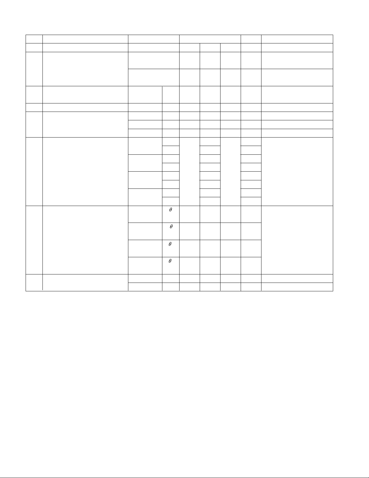
• l Option adjustment following BOM
- Tool Option1
- Tool Option2
- Area Option
(Fig. 1)
1) Push the ADJ key in the Adjust Remocon.
2) Input the Option Number that was specified in the BOM,
into the Shipping area
3) Select "Tool Option1/ Tool Option2/ Area Option" by using
/ °„/°Â(CH+/-) key , and press the number key(0~9)
consecutively
ex) If the value of Tool Option1 is 7, input the data using
number key "7" (Fig. 1)
3.2 SET assembly adjustment items
• Auto AV1 Color Balance
• Adjustment of White Balance
• Auto Component Color Balance adjustment
- standard equipment : MSPG925FA
• Auto RGB Color Balance adjustment
-standard equipment : MSPG925FA
4. EDID
4.1 Caution
* Use the proper signal cable for EDID Downloa.
- Analog EDID : Pin3 exists
- Digital EDID : Pin3 exists
*Caution: - Never connect HDMI & DVI-D & DVI-A Cable at
the same time.
- Use the proper cables below for EDID Writing
- Write 8bit using DDC2B protocol to input
ANALOG,HDMI EDID.
4.1.1 EDID Data
4.2 Data
4.2.1. 47LC7R-TA ANALOG
• BLOCK1 (128BYTE)
4.2.2. 47LC7R-TA HDMI1
• BLOCK1 (128BYTE)
• BLOCK2 (128BYTE)
No Item Condition 16 Data
1 Manufacturer ID GSM 1E6D
2 Version Digital: 1 01
3 Revision Digital: 3 03
Page 11
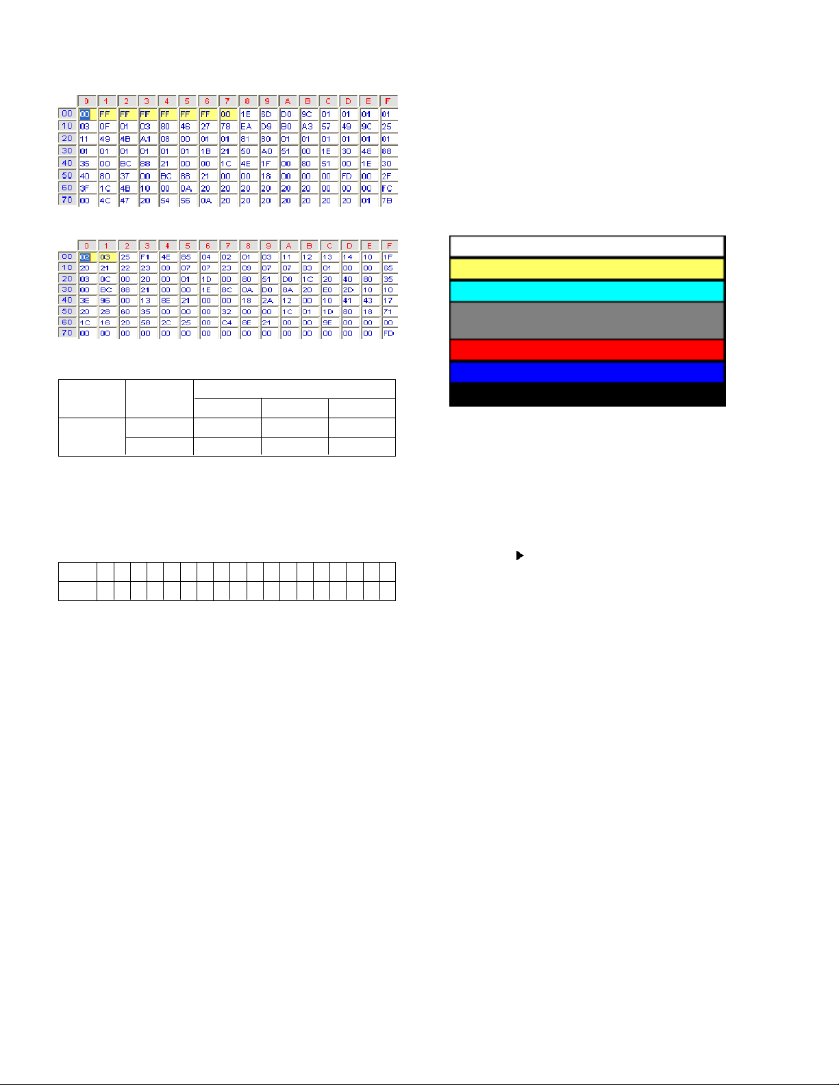
4.2.3. 47LC7R-TA HDMI2
• BLOCK1 (128BYTE)
• BLOCK2 (128BYTE)
=> Detail EDID Options are below (a, b, c, d, e).
a. Product ID
b. Serial No: Controlled on production line
c. Month, Year: Controlled on production line:
ex) Montly: ‘03’ => ‘03’
Year: ‘2005’ => ‘0F’
d. Model Name/Monitor Name
e. Checksum: Changeable by total EDID data
5. ADC Calibration
5.1 Adjustment of AV
* Required Equipments
• Remote controller for adjustment
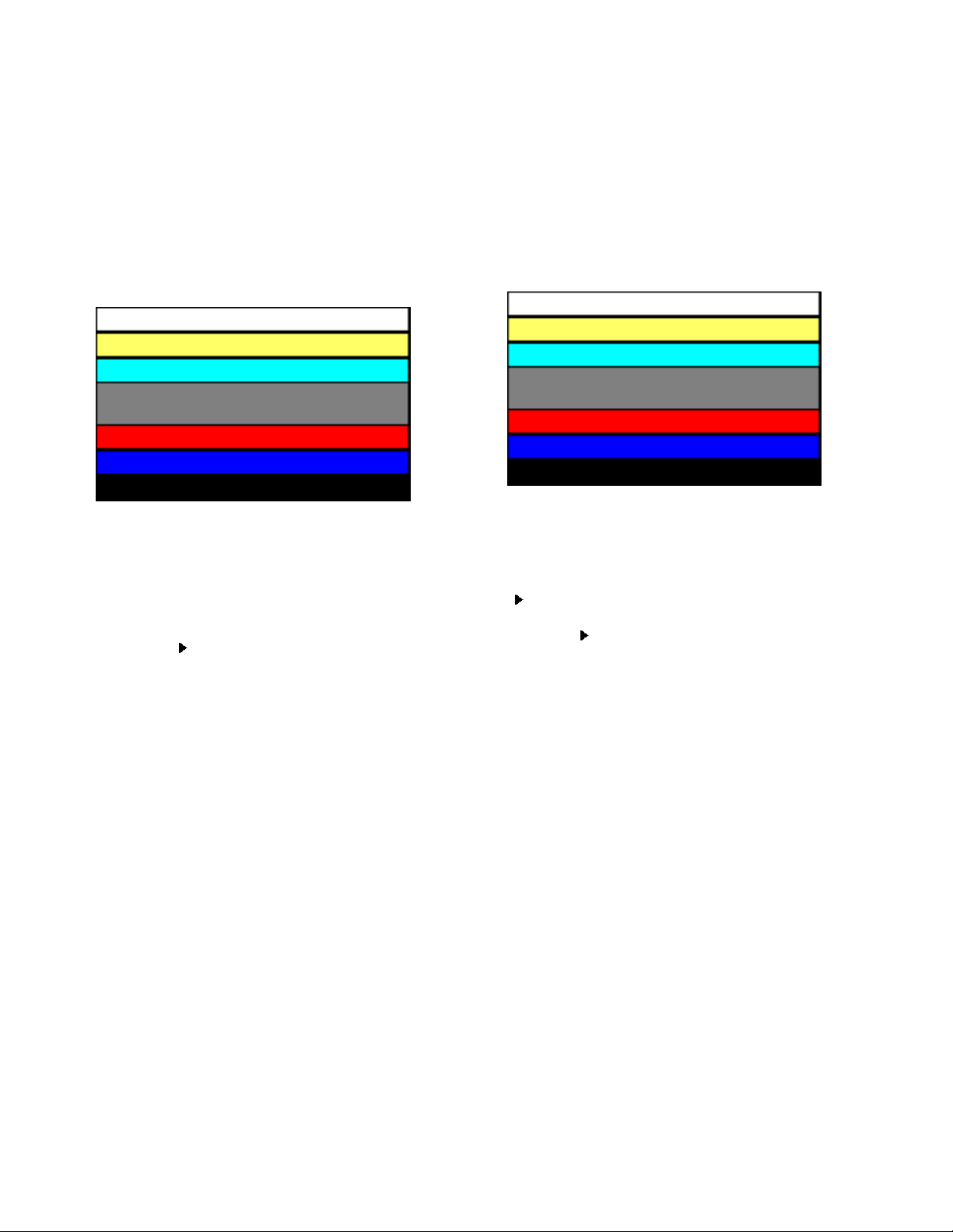
• 802F Pattern Generator, Master (MSPG-925FA), etc
• MSPG-925FA Pattern Generator
(Which has Video Signal: 100% Color Bar Pattern
shown in Fig. 1)
=> Model: 202 / Pattern: 65 (PAL : CH).
Model: 207 / Pattern : 65 (NTSC-J).
(Fig. 1)
5.1.1 Method of Auto AV Color Balance
1) Press the FRONT-AV KEY on R/C for converting input
mode.
2) Input the Video Signal: 100% Color Bar signal into
AV(MA/TA)
3) Set the PSM to Dynamic mode in the Picture menu
4) Press INSTART key on R/C for adjustment
5) Press the
(Vol. +) key to operate the set, then it
becomes automatically
6) Auto-RGB OK means the adjustment is completed
5.1.2 Requirement
• This AV color balance adjustment should be performed
before White Balance Adjustment.
- 11 -
Copyright © 2007 LG Electronics. Inc. All right reserved.
Only for training and service purposes
LGE Internal Use Only
Model Name
Product ID
Product ID
Dec. Hex. EDID Tabla
47LC7R-TA
40143(A) 40143 9CCF CF9C
40144(D) 40144 9CD0 D09C
Model
47LC7R 00 00 00 FC 00 4C 47 20 54 56 0A 20 20 20 20 20 20 20
Page 12
Copyright © 2007 LG Electronics. Inc. All right reserved.
Only for training and service purposes
LGE Internal Use Only
- 12 -
5.2 Adjustment of Component.
* Required Equipments
• Remote controller for adjustment.
• 802F Pattern Generator, Master (MSPG-925FA), etc.
• MSPG-925FA Pattern Generator
(Which has 720p@50Hz YPbPr signal : 100% Color
Bar Pattern shown in Fig. 2).
=> Model: 215 / Pattern: 65
• It is very import to use correct adjustment pattern like
Fig. 2.
# If Minimum Black Level and/or Maximum White Level
is not correct, Do select 100% Color Bar Pattern.
(Fig. 2)
5.2.1 Method of Auto Component Color Balance
1) Input the Component 720p 100% Color Bar(MSPG-925FA
model:215, pattern:65) signal into Component ( ZA :
component , TA/MA : component 1 or 2)
2) Set the PSM to Dynamic mode in the Picture menu.
3) Press the INSTART key on R/C for adjustment.
4) Press the
(Vol. +) key to operate the set , then it
becomes automatically.
5) Auto-RGB OK means the adjustment is completed
5.3 Adjustment of RGB)
* Required Equipments
• Remote controller for adjustm
• 802F Pattern Generator, Master (MSPG-925FA), etc
• MSPG-925FA Pattern Generator
(Which has XGA [1024*768] 60Hz PC Format output
signal : 100% Color Bar Pattern shown in Fig. 3 )
• It is very import to use correct adjustment pattern like
Fig. 10.
# If Minimum Black Level and/or Maximum White Level
is not correct, Do select 100% Color Bar Pattern.
(Fig. 3)
5.3.1 Method of Auto RGB Color Balance
1) Input the PC 1024x768 @ 60Hz with 100% color bar
pattern like Fig.3. into RGB.
2)
Set the PSM to Dynamic mode in Picture menu
3) Press the INSTART key on R/C for adjustment.
4) Press the
(Vol. +) key operate To set , then it becomes
automatically
5) Auto-RGB OK means adjustment is completed
Page 13

Copyright © 2007 LG Electronics. Inc. All right reserved.
Only for training and service purposes
LGE Internal Use Only
- 13 -
6. White Balance
*Notice
- Do the white balance adjustment under the 10LUX.
- Before white balance,press the In-start key 2times and do
the reset like Fig1
- Use the cortez inner pattern(216 gray pattern)
- To enter White-balance mode,press the IN-START key
2times
=> Caution : - System control RS-232 Host should be "PC"
for adjustment
* Test Equipment
- Color Analyzer ( CA-210)
- PC (for communication through RS-232C) => UART
Baud rate : 115200
- Pattern Generator (MSPG-925FA etc.)
* Color Temperature & Color Coordinates Setting
: When adjusting the Color Temperature of LCD, Color
AnalyzerCA-210(Matrix should be corrected through CH9
of CS-1000) should be used.
Adjust the Color Temperature based below adjustment
color coordinates.
Even if CH9 of CA-210 is corrected with Matrix, there may
be many character of Module and Filter.
Therefore Refer to the below Color Coordinates Target.
But,in case of WCG module,use the CH12 of CA-210.
6.1 Manual white Balance (INNER PATTERN)
1) Execute CA-210(9CH) Zero Calibration
2) Execute the SET Heat Run for 30minutes
3) Use cortez inner pattern as below Fig. 4, Supply 216Level
(85 IRE) full screen pattern
4) Enter the White Balance adjustment mode by pressing the
INSTART key twice(White Balance) on R/C.
5) Stick sensor to center of the screen and select each items
(Red/Green/Blue Gain and Offset) using
/ (CH+/-) key
on R/C.
6) Adjust with R / G / B Gain using
/ key on R/C.
7) Adjust it until color coordination becomes as below.
*Color Temperature : Cool, Medium, Warm
One of R/G.B Gain should be fixed at 80 and adjust two Gain
Value with decreasing the Default values from 80.
-When R Gain is Fixed at Default value(80)
Adjust G gain and B gain with decreasing Default values from 80
-When B Gain is Fixed at Default value(80)
Adjust R gain and G gain with decreasing Default values from 80
-When G Gain is Fixed at Default value(80)
Adjust R gain and B gain with decreasing Default values from 80
R/G/B Gain and R/G/B Offset Default Value
Red Gain : 80 , Green Gain : 80, Blue Gain : 80
(Fig. 4)
216 Level (85IRE)
Page 14

6.2 Auto white Balance (INNER PATTERN)
- 14 -
Copyright © 2007 LG Electronics. Inc. All right reserved.
Only for training and service purposes
LGE Internal Use Only
command1 command2 Set ID
Data
MODE
Input Select x b 00 00h DTV-Air
01h Cable
10h RF-Air
11h Cable
20h AV1
21h AV2
40h COMP1
41h COMP1
60h RGB-PC
90h HDMI
Min Max INIT
R-Gain_Normal j a 00 00h 80h 80h
G-Gain_Normal j b 00 00h 80h 80h
B-Gain_Normal j c 00 00h 80h 80h
R-Gain_Warm j d 00 00h 80h 80h
G-Gain_Warm j e 00 00h 80h 80h
B-Gain_Warm j f 00 00h 80h 80h
R-Gain_Cool j g 00 00h 80h 80h
G-Gain_Cool j h 00 00h 80h 80h
B-Gain_Cool j i 00 00h 80h 80h
R-Offset_Normal l j 00 00h 80h
G-Offset_Normal l k 00 00h 80h
B-Offset_Normal l l 00 00h 80h
R-Offset_Warm l m 00 00h 80h
G-Offset_Warm l n 00 00h 80h
B-Offset_Warm l o 00 00h 80h
R-Offset_Cool l p 00 00h 80h
G-Offset_Cool l q 00 00h 80h
B-Offset_Cool l r 00 00h 80h
COLOR TEMP. k u 00 00h 03h(Cool,Normal,Warm,User)
Signal Inside Pattern w b 00 00 W/B Adjustment Start
10 Using Internal Pattern
ff W/B Adjustment Comletion
Page 15

Copyright © 2007 LG Electronics. Inc. All right reserved.
Only for training and service purposes
LGE Internal Use Only
- 15 -
TROUBLESHOOTING
1. No Raster - LCD
(1) Symptom
1) Does’t minute discharge at module.
2) It maintains the condition where the front LED is normal.
(2) Check follow
Is the Inverter
On or Off
Check the Power board.
Off
No
Is the
inverter 24V on power
board normal
No
No No
No
Is output
the normality Low/High
voltage except
stand-by 5V?
No
'Inverter_On'
Signal is High of 5
th
pin in
P1001 on
Main board
Yes
On
Yes
Is the link cable
normal?
1. Check the Inverter connector
2. Check the LCD Module
Yes
1. Check the Main Board.
1. Reconnect the link cable in
P1301
No
1. Check the Main board
1. Change the Power Board
1. Change the Main Board
Yes
Is the Power Board
normal?
Yes
Is the VSC Board
normal?
Is the P1301's output
normal?
Page 16

Copyright © 2007 LG Electronics. Inc. All right reserved.
Only for training and service purposes
LGE Internal Use Only
- 16 -
Is the LVDS cable
normal?
Is the VSC Board
normal?
IC800' operation
is normal?
Is the Ctrl Board of
Module normal?
Is the LVDS cable
connected well?
Replace cable.
Replace VSC B/D
No
No Yes
Replace Ctrl Board in Plasma panel
No
Replace LCD Module
No
Yes
Yes
Is the LCD Module
normal?
Yes
Plasma
LCD TV
No
Cable inserts well.
No
Replace FIL8668 IC(IC800).
2. In case of occur strange screen into specific mode
2-1. In case of doesn’t display the OSD
(1) Symptom
1) LED is White
2) The minute discharge work continuously
(2) Check follow
Page 17

Copyright © 2007 LG Electronics. Inc. All right reserved.
Only for training and service purposes
LGE Internal Use Only
- 17 -
2-2. In the case of doesn't work normally at specific input mode
(1) Symptom
1) The screen doesn't work normally at specific input mode (RF, AV, Component, RGB, HDMI)
(2) Check follow
1) Check the all input model if all input display normally.
2) Check the PIP and Double Window if it display normally.(Re-Check it Swap)
(3) In case of unusual situation from RF mode
Is the Tuner normal?
No
Yes
Yes
Cable inserts well.
Replace Tuner
Replace IC611
Is the Tuner Cable
connected well?
No
Is the Input voltage,
IIC Communication and
HV sync normal?
No
No
Is normal the
Input voltage, IIC
Communication and CVBS
output?
No
No
Is the IC611
normal?
Replace IC800
No
Is the Input voltage,
IIC Communication and
HV sync normal?
No
Is the IC800
normal?
Page 18

Copyright © 2007 LG Electronics. Inc. All right reserved.
Only for training and service purposes
LGE Internal Use Only
- 18 -
(4) When set doesn’t display normally at RF , AV mode
(5) When set doesn't display nromally at Component, RGB mode
(6) In the case of becomes unusual display from HDMI mode
Yes
Replace IC1200
No
Is the Input voltage,
IIC Communication and
HV sync normal?
No
Is the IC1200
normal?
Replace IC800
No
Is the Input voltage,
IIC Communication and
HV sync normal?
No
Is the IC800
normal?
Replace IC800
No
Is the Input voltage,
IIC Communication and
HV sync normal?
No
Is the IC800
normal?
Yes
Replace IC611
No
Is the Input voltage,
IIC Communication and
HV sync normal?
No
Is the IC611
normal?
Replace IC800
No
Is the Input voltage,
IIC Communication and
HV sync normal?
No
Is the IC800
normal?
Page 19

Copyright © 2007 LG Electronics. Inc. All right reserved.
Only for training and service purposes
LGE Internal Use Only
- 19 -
3. In case of no sound
(1) Symptom
1) LED is White
2) Screen existent, but Sound isn’t
(2) Check follow
No
No No
All input(mode)
is no sound?
Only HDMI is
no sound?
Replace IC400
Replace IC401
Replace
VSC B/D
Set on speaker in menu
Download the EDID data
Check the speaker cable
No
Only RF is
no sound?
Check the Tuner In/Out
No
No
No
Replace IC402
No
Is the Speaker
on in Menu?
Yes
Yes
Yes
Is the speaker
cable normal?
Yes Yes
Yes Yes
IC1401 operate
normally?
IC1401 operate
normally?
IC402 operate
normally?
Page 20

BLOCK DIAGRAM
- 20 -
Copyright © 2007 LG Electronics. Inc. All right reserved.
Only for training and service purposes
LGE Internal Use Only
Page 21

Copyright © 2007 LG Electronics. Inc. All right reserved.
Only for training and service purposes
LGE Internal Use Only
- 21 -
EXPLODED VIEW
300
121
120
710
500
510
121
700
200
LV1
803
800
804
600
520
610
840
830
910
900
400
530
820
806
805
802
801
807
A2
A21
Page 22

Copyright © 2007 LG Electronics. Inc. All right reserved.
Only for training and service purposes
LGE Internal Use Only
- 22 -
EXPLODED VIEW PARTS LIST
No.
PART NO.
DESCRIPTION
120 EAB33775103
Speaker,Full Range, EN1562C-6723 ND 10W 8OHM 82DB 100HZ 187 X 42 X 39.9 LUG KOREA TOPTONE
121 EAB33893101
Speaker,Tweeter, EN10D-6714 ND 10W 8OHM 82DB 0HZ 68 X 23 X 22.7 LUG KOREA TOPTONE
200 EAJ38000101
LCD,Module-TFT, LC470WX1-SLA1 WXGA 47INCH 1366X768 500CD COLOR 72% 16/9 1000:1(basic) P7 ZRT 8bit 20% dimming 10000K LG PHILIPS LCD
300 ABJ33147804 Cabinet Assembly, 47LB9DF-UD - 47" CABINET ASS'Y SET, NON PET NAME
400 ACQ33147605 Cover Assembly,Rear, 47LB9R-TD LP7AA 47" BACK COVER ASSY
500 EBR36401901 PCB Assembly, SUB T.T LP7AA 47LB7RF IR .
510 EBR36402804 PCB Assembly, SUB T.T LP7AA 47LB9R CONTROL KEY .
520 EBR36401307 PCB Assembly, SUB T.T LP7AA 47LB9R SIDE AV ..
530 EBR36524801 PCB Assembly,Sub, SUB T.T LA71A 42LY3DR-NA AKRLLH AC-Inlet Ass'y Total
600 EAY32816901
SMPS,AC/DC, FSP327-6F01 90VTO264V 375W 50/60 CB, UL, IEC600,650 etc... LCD 47inch SPI PSU for New chassis(E3 etc...) FSP Technology Inc.
610 EBU38726401 Main Total Assembly, 47LC7R BRAND LP7AB
700 6500VR0003E
Sensor,Ambient Light, YGCA-T071C 12 HOUSING BK 26.4X20X26.4mm VOUT 5V(AT 80LUX) LG INNOTEK CO., LTD
710 MES36332302 Indicator, MOLD ABS LED&PRE AMP 32LB9 PMMA 7 PHY SMOKE BLACK PRINTING
800 MGJ37965102 Plate,Metal, PRESS SBHG1 1.6 METAL EGI 47LB9DF-UA
801 MGJ32889606 Plate,Metal, PRESS SBHG1 1.6 METAL EGI BAR BOTTOM (47LB9)
802 MGJ32889801 Plate,Metal, PRESS SBHG1 1.6 METAL EGI BAR LEFT (47LY3)
803 MGJ32897002 Plate,Metal, PRESS SBHGI 1.6 METAL EGI BAR CENTER (47LY3)
804 MGJ32890002 Plate,Metal, PRESS SBHG1 1.6 METAL EGI BAR RIGHT (47LB4, PEM-NUT 'YES')
805 MGJ32897102 Plate,Metal, PRESS SBHG1 1.6 METAL EGI BAR SIDE TOP (47LY3) H4_NON_EU
806 MGJ32897202 Plate,Metal, PRESS SBHG1 1.6 METAL EGI BAR SIDE BOTTOM (47LY3) H4_NON_EU
807 AGU34582001 Plate Assembly, SUPPORTER 47LB9_PLATE ASSEMBLY
820 MGJ38662501 Plate,Shield, PRESS SAZCC 0.6 SHIELD EGI SAZCC 0.6t(206x245)
830 MGJ37663501 Plate,Shield, PRESS SPTE 0.5 SHIELD SPTE 52LY3 POWER SHIELD
840 MGJ37663602 Plate,Shield, PRESS SPTE 0.5 SHIELD SPTE 47LB7RF-TA H4-H SHIELD COVER "TYPE B"
900 AAN33146802 Base Assembly, STAND 47LB9DF-AD LA71A ASSY, NON HAIR LINE, GLOSSY BLACK, SET
910 ABA32985001 Bracket Assembly, STAND 32LB9D-UA LA73A 32LB9
A2 MKJ32022837 Remote Controller, COMPLEX LP7AA 47LB7RF-TB H4,FULL HD,CONTINENT OF ASIA
A21 3550V00590A Cover, MOLD ABS 50PC3DD-UE.AUSRSHR ABS -
LV1 EAD35683003
Harness,Single, LVDS LPL STD_300MM FI-X30HL(JAE) 12507HS-30(YeonHo) 300mm 1.25MM 30P-30P UL20276 AWG30 TWI N H4 UNIXTAR TECHNOLOGY INC.
Page 23

Copyright © 2007 LG Electronics. Inc. All right reserved.
Only for training and service purposes
LGE Internal Use Only
- 23 -
A1 MFL37457711 "Manual,Owners" PRINTING USER LP7AA BR
A2 MKJ32022837 Remote Controller COMPLEX LP7AA 47LB7RF-
A21 3550V00590A Cover MOLD ABS 50PC3DD-UE.AU
A3 EAD36223201 Power Cord SP023+IS15 SP-023 IS-1
A4 SAC30653102 Title LP7AA_PP7AA H4 NEU EN(
C1015 0CE477WF6DC "Capacitor,AL,Chip" MVK10TP16VC470M 470uF
C1016 0CE227WF6DC "Capacitor,AL,Chip" MVK8.0TP16VC220M 220uF
C1017 0CE337WJ6D8 "Capacitor,AL,Chip" MVK12.5TP35VC330M 330u
C1019 0CE477WF6DC "Capacitor,AL,Chip" MVK10TP16VC470M 470uF
C102 0CE227SF6DC "Capacitor,AL,Chip" MVG6.3TP16VC220M 220uF
C1023 0CE477WF6DC "Capacitor,AL,Chip" MVK10TP16VC470M 470uF
C1036 0CE477WF6DC "Capacitor,AL,Chip" MVK10TP16VC470M 470uF
C1038 0CE477WF6DC "Capacitor,AL,Chip" MVK10TP16VC470M 470uF
C1057 0CZZTAT002B "Capacitor,AL,Chip" 10SVP47M 47uF 20% 10V
C1062 0CE477WF6DC "Capacitor,AL,Chip" MVK10TP16VC470M 470uF
C1064 0CE477WF6DC "Capacitor,AL,Chip" MVK10TP16VC470M 470uF
C1070 0CE477WF6DC "Capacitor,AL,Chip" MVK10TP16VC470M 470uF
C1096 0CE476WF6DC "Capacitor,AL,Chip" MVK6.3TP16VC47M 47uF 2
C1100 0CE476WF6DC "Capacitor,AL,Chip" MVK6.3TP16VC47M 47uF 2
C1104 0CE107WF6DC "Capacitor,AL,Chip" MVK6.3TP16VC100M 100uF
C111 0CE227SF6DC "Capacitor,AL,Chip" MVG6.3TP16VC220M 220uF
C1112 0CE107WF6DC "Capacitor,AL,Chip" MVK6.3TP16VC100M 100uF
C112 0CE106WH6DC "Capacitor,AL,Chip" MVK5.0TP25VC10M 10uF 2
C1124 0CE226WF6DC "Capacitor,AL,Chip" MVK5.0TP16VC22M 22uF 2
C1125 0CE226WF6DC "Capacitor,AL,Chip" MVK5.0TP16VC22M 22uF 2
C1126 0CE107WF6DC "Capacitor,AL,Chip" MVK6.3TP16VC100M 100uF
C1128 0CE107WF6DC "Capacitor,AL,Chip" MVK6.3TP16VC100M 100uF
C113 0CE106WH6DC "Capacitor,AL,Chip" MVK5.0TP25VC10M 10uF 2
C1131 0CE107WF6DC "Capacitor,AL,Chip" MVK6.3TP16VC100M 100uF
C1143 0CE477WF6DC "Capacitor,AL,Chip" MVK10TP16VC470M 470uF
C115 0CE227SF6DC "Capacitor,AL,Chip" MVG6.3TP16VC220M 220uF
C1201 0CE476WF6DC "Capacitor,AL,Chip" MVK6.3TP16VC47M 47uF 2
C1207 0CE476WF6DC "Capacitor,AL,Chip" MVK6.3TP16VC47M 47uF 2
C1222 0CE106WH6DC "Capacitor,AL,Chip" MVK5.0TP25VC10M 10uF 2
C1226 0CE106WH6DC "Capacitor,AL,Chip" MVK5.0TP25VC10M 10uF 2
C1244 0CE106WH6DC "Capacitor,AL,Chip" MVK5.0TP25VC10M 10uF 2
C1401 0CE106WFKDC "Capacitor,AL,Chip" MVK4.0TP16VC10M 10uF 2
C1406 0CE106WFKDC "Capacitor,AL,Chip" MVK4.0TP16VC10M 10uF 2
C1420 0CE106WFKDC "Capacitor,AL,Chip" MVK4.0TP16VC10M 10uF 2
C1814 0CE226WF6DC "Capacitor,AL,Chip" MVK5.0TP16VC22M 22uF 2
C1820 0CE105WK6DC "Capacitor,AL,Chip" MVK4.0TP50VC1M 1uF 20%
C1840 0CE105WK6DC "Capacitor,AL,Chip" MVK4.0TP50VC1M 1uF 20%
C202 0CE106WFKDC "Capacitor,AL,Chip" MVK4.0TP16VC10M 10uF 2
C213 0CE227SF6DC "Capacitor,AL,Chip" MVG6.3TP16VC220M 220uF
C215 0CE106WFKDC "Capacitor,AL,Chip" MVK4.0TP16VC10M 10uF 2
C223 0CE227SF6DC "Capacitor,AL,Chip" MVG6.3TP16VC220M 220uF
C404 0CE106WFKDC "Capacitor,AL,Chip" MVK4.0TP16VC10M 10uF 2
C405 0CE107WF6DC "Capacitor,AL,Chip" MVK6.3TP16VC100M 100uF
C409 0CE226WF6DC "Capacitor,AL,Chip" MVK5.0TP16VC22M 22uF 2
C412 0CE335WK6D8 "Capacitor,AL,Chip" MVK4.0TP50VC3.3M 3.3uF
C420 0CE106WFKDC "Capacitor,AL,Chip" MVK4.0TP16VC10M 10uF 2
C421 0CE475WK6DC "Capacitor,AL,Chip" MVK5.0TP50VC4.7M 4.7uF
C422 0CE475WK6DC "Capacitor,AL,Chip" MVK5.0TP50VC4.7M 4.7uF
C423 0CE107WF6DC "Capacitor,AL,Chip" MVK6.3TP16VC100M 100uF
C432 0CE226WF6DC "Capacitor,AL,Chip" MVK5.0TP16VC22M 22uF 2
C446 0CE335WK6D8 "Capacitor,AL,Chip" MVK4.0TP50VC3.3M 3.3uF
C451 0CE106WH6DC "Capacitor,AL,Chip" MVK5.0TP25VC10M 10uF 2
C452 0CE106WH6DC "Capacitor,AL,Chip" MVK5.0TP25VC10M 10uF 2
C466 0CE475WK6DC "Capacitor,AL,Chip" MVK5.0TP50VC4.7M 4.7uF
C467 0CE475WK6DC "Capacitor,AL,Chip" MVK5.0TP50VC4.7M 4.7uF
C616 0CE476WF6DC "Capacitor,AL,Chip" MVK6.3TP16VC47M 47uF 2
C621 0CE226WF6DC "Capacitor,AL,Chip" MVK5.0TP16VC22M 22uF 2
C628 0CE107WF6DC "Capacitor,AL,Chip" MVK6.3TP16VC100M 100uF
C834 0CE226WF6DC "Capacitor,AL,Chip" MVK5.0TP16VC22M 22uF 2
C835 EAE30840301 "Capacitor,AL,Chip" 10SVPC68M 68uF 20% 10V
C836 0CE226WF6DC "Capacitor,AL,Chip" MVK5.0TP16VC22M 22uF 2
C837 0CE226WF6DC "Capacitor,AL,Chip" MVK5.0TP16VC22M 22uF 2
C838 0CE226WF6DC "Capacitor,AL,Chip" MVK5.0TP16VC22M 22uF 2
C839 0CE226WF6DC "Capacitor,AL,Chip" MVK5.0TP16VC22M 22uF 2
C840 0CE226WF6DC "Capacitor,AL,Chip" MVK5.0TP16VC22M 22uF 2
C842 0CE226WF6DC "Capacitor,AL,Chip" MVK5.0TP16VC22M 22uF 2
C853 EAE30840301 "Capacitor,AL,Chip" 10SVPC68M 68uF 20% 10V
C855 0CE226WF6DC "Capacitor,AL,Chip" MVK5.0TP16VC22M 22uF 2
C886 0CE226WF6DC "Capacitor,AL,Chip" MVK5.0TP16VC22M 22uF 2
C898 EAE30840301 "Capacitor,AL,Chip" 10SVPC68M 68uF 20% 10V
C901 EAE30840301 "Capacitor,AL,Chip" 10SVPC68M 68uF 20% 10V
C904 EAE30840301 "Capacitor,AL,Chip" 10SVPC68M 68uF 20% 10V
C905 EAE30840301 "Capacitor,AL,Chip" 10SVPC68M 68uF 20% 10V
C950 0CE226WF6DC "Capacitor,AL,Chip" MVK5.0TP16VC22M 22uF 2
C967 EAE30840301 "Capacitor,AL,Chip" 10SVPC68M 68uF 20% 10V
C968 EAE30840301 "Capacitor,AL,Chip" 10SVPC68M 68uF 20% 10V
C969 EAE30840301 "Capacitor,AL,Chip" 10SVPC68M 68uF 20% 10V
C1423 0CE477BJ618 "Capacitor,AL,Radial" ESM477M035T1G5H20G 470
C100 0CH5681K416 "Capacitor,Ceramic,Chip" C2012C0G1H681JT 680pF
C1001 0CK104CK56A "Capacitor,Ceramic,Chip" 0603B104K500CT 100nF 1
C1003 0CK474CH94A "Capacitor,Ceramic,Chip" 0603F474Z250CT 470nF -
C1004 0CK474CH94A "Capacitor,Ceramic,Chip" 0603F474Z250CT 470nF -
C1007 0CK104CK56A "Capacitor,Ceramic,Chip" 0603B104K500CT 100nF 1
C101 0CH3104K566 "Capacitor,Ceramic,Chip" 0805B104K500CT 100nF 1
C101 0CH5101K416 "Capacitor,Ceramic,Chip" C2012C0G1H101JT 100pF
C102 0CC102CK41A "Capacitor,Ceramic,Chip" C1608C0G1H102JT 1nF 5%
C102 0CH5101K416 "Capacitor,Ceramic,Chip" C2012C0G1H101JT 100pF
C1020 0CK104CK56A "Capacitor,Ceramic,Chip" 0603B104K500CT 100nF 1
C1024 0CK104CK56A "Capacitor,Ceramic,Chip" 0603B104K500CT 100nF 1
C1025 0CK103CK56A "Capacitor,Ceramic,Chip" 0603B103K500CT 10nF 10
C103 0CC102CK41A "Capacitor,Ceramic,Chip" C1608C0G1H102JT 1nF 5%
LOC. NO. PART NO. DESCRIPTION / SPECIFICATION LOC. NO. PART NO. DESCRIPTION / SPECIFICATION
REPLACEMENT PARTS LIST
DATE: 2007. 10. 12.
CAPACITORs
ACCESSORY
Page 24

- 24 -
C103 0CH5681K416 "Capacitor,Ceramic,Chip" C2012C0G1H681JT 680pF
C103 0CH6330K416 "Capacitor,Ceramic,Chip" C2012C0G1H330JT 33pF 5
C1037 0CK103CK51A "Capacitor,Ceramic,Chip" 0603B103K500CT 10nF 10
C1039 0CK104CK56A "Capacitor,Ceramic,Chip" 0603B104K500CT 100nF 1
C104 0CH5681K416 "Capacitor,Ceramic,Chip" C2012C0G1H681JT 680pF
C1059 0CK104CK56A "Capacitor,Ceramic,Chip" 0603B104K500CT 100nF 1
C1063 0CK104CK56A "Capacitor,Ceramic,Chip" 0603B104K500CT 100nF 1
C1065 0CK104CK56A "Capacitor,Ceramic,Chip" 0603B104K500CT 100nF 1
C1065 0CK104CK56A "Capacitor,Ceramic,Chip" 0603B104K500CT 100nF 1
C1069 0CK104CK56A "Capacitor,Ceramic,Chip" 0603B104K500CT 100nF 1
C1069 0CK104CK56A "Capacitor,Ceramic,Chip" 0603B104K500CT 100nF 1
C107 0CC102CK41A "Capacitor,Ceramic,Chip" C1608C0G1H102JT 1nF 5%
C108 0CC102CK41A "Capacitor,Ceramic,Chip" C1608C0G1H102JT 1nF 5%
C1102 0CK104CK56A "Capacitor,Ceramic,Chip" 0603B104K500CT 100nF 1
C1115 0CK104CK56A "Capacitor,Ceramic,Chip" 0603B104K500CT 100nF 1
C1115 0CK104CK56A "Capacitor,Ceramic,Chip" 0603B104K500CT 100nF 1
C1120 0CK104CK56A "Capacitor,Ceramic,Chip" 0603B104K500CT 100nF 1
C1122 0CK104CK56A "Capacitor,Ceramic,Chip" 0603B104K500CT 100nF 1
C1122 0CK104CK56A "Capacitor,Ceramic,Chip" 0603B104K500CT 100nF 1
C1127 0CK104CK56A "Capacitor,Ceramic,Chip" 0603B104K500CT 100nF 1
C1129 0CK104CK56A "Capacitor,Ceramic,Chip" 0603B104K500CT 100nF 1
C1130 0CK104CK56A "Capacitor,Ceramic,Chip" 0603B104K500CT 100nF 1
C1132 0CK104CK56A "Capacitor,Ceramic,Chip" 0603B104K500CT 100nF 1
C1134 0CK104CK56A "Capacitor,Ceramic,Chip" 0603B104K500CT 100nF 1
C1135 0CK104CK56A "Capacitor,Ceramic,Chip" 0603B104K500CT 100nF 1
C1136 0CK225DH94A "Capacitor,Ceramic,Chip" C2012Y5V225ZFT 2.2uF -
C1139 0CK103CK56A "Capacitor,Ceramic,Chip" 0603B103K500CT 10nF 10
C1142 0CK104CK56A "Capacitor,Ceramic,Chip" 0603B104K500CT 100nF 1
C1144 0CK104CK56A "Capacitor,Ceramic,Chip" 0603B104K500CT 100nF 1
C116 0CK471CK56A "Capacitor,Ceramic,Chip" C1608X7R1H471KT 470pF
C117 0CK471CK56A "Capacitor,Ceramic,Chip" C1608X7R1H471KT 470pF
C1200 0CK104CK56A "Capacitor,Ceramic,Chip" 0603B104K500CT 100nF 1
C1205 0CK104CK56A "Capacitor,Ceramic,Chip" 0603B104K500CT 100nF 1
C1212 0CK104CK56A "Capacitor,Ceramic,Chip" 0603B104K500CT 100nF 1
C1213 0CK104CK56A "Capacitor,Ceramic,Chip" 0603B104K500CT 100nF 1
C1214 0CK104CK56A "Capacitor,Ceramic,Chip" 0603B104K500CT 100nF 1
C1215 0CK104CK56A "Capacitor,Ceramic,Chip" 0603B104K500CT 100nF 1
C1216 0CK102CK56A "Capacitor,Ceramic,Chip" 0603B102K500CT 1nF 10%
C1217 0CK102CK56A "Capacitor,Ceramic,Chip" 0603B102K500CT 1nF 10%
C1218 0CK102CK56A "Capacitor,Ceramic,Chip" 0603B102K500CT 1nF 10%
C1219 0CK102CK56A "Capacitor,Ceramic,Chip" 0603B102K500CT 1nF 10%
C1220 0CK102CK56A "Capacitor,Ceramic,Chip" 0603B102K500CT 1nF 10%
C1221 0CK102CK56A "Capacitor,Ceramic,Chip" 0603B102K500CT 1nF 10%
C1223 0CC180CK41A "Capacitor,Ceramic,Chip" C1608C0G1H180JT 18pF 5
C1224 0CK103CK56A "Capacitor,Ceramic,Chip" 0603B103K500CT 10nF 10
C1225 0CC180CK41A "Capacitor,Ceramic,Chip" C1608C0G1H180JT 18pF 5
C1228 0CK103CK51A "Capacitor,Ceramic,Chip" 0603B103K500CT 10nF 10
C1235 0CK102CK56A "Capacitor,Ceramic,Chip" 0603B102K500CT 1nF 10%
C1236 0CK102CK56A "Capacitor,Ceramic,Chip" 0603B102K500CT 1nF 10%
C1237 0CK102CK56A "Capacitor,Ceramic,Chip" 0603B102K500CT 1nF 10%
C1238 0CK102CK56A "Capacitor,Ceramic,Chip" 0603B102K500CT 1nF 10%
C1239 0CK102CK56A "Capacitor,Ceramic,Chip" 0603B102K500CT 1nF 10%
C1240 0CK102CK56A "Capacitor,Ceramic,Chip" 0603B102K500CT 1nF 10%
C1241 0CK102CK56A "Capacitor,Ceramic,Chip" 0603B102K500CT 1nF 10%
C1242 0CK102CK56A "Capacitor,Ceramic,Chip" 0603B102K500CT 1nF 10%
C1243 0CK102CK56A "Capacitor,Ceramic,Chip" 0603B102K500CT 1nF 10%
C1245 0CK104CK56A "Capacitor,Ceramic,Chip" 0603B104K500CT 100nF 1
C1246 0CK104CK56A "Capacitor,Ceramic,Chip" 0603B104K500CT 100nF 1
C1247 0CK104CK56A "Capacitor,Ceramic,Chip" 0603B104K500CT 100nF 1
C1248 0CK104CK56A "Capacitor,Ceramic,Chip" 0603B104K500CT 100nF 1
C1403 0CK104CK56A "Capacitor,Ceramic,Chip" 0603B104K500CT 100nF 1
C1405 0CK104CK56A "Capacitor,Ceramic,Chip" 0603B104K500CT 100nF 1
C1410 0CK104CK56A "Capacitor,Ceramic,Chip" 0603B104K500CT 100nF 1
C1411 0CK104CK56A "Capacitor,Ceramic,Chip" 0603B104K500CT 100nF 1
C1412 0CC101CK41A "Capacitor,Ceramic,Chip" C1608C0G1H101JT 100pF
C1413 0CC102CK41A "Capacitor,Ceramic,Chip" C1608C0G1H102JT 1nF 5%
C1419 0CK105CF94A "Capacitor,Ceramic,Chip" 0603F105Z160CT 1uF -20
C1421 0CK223CK56A "Capacitor,Ceramic,Chip" UMK107JB223KA-T 22nF 1
C1422 0CK104CK56A "Capacitor,Ceramic,Chip" 0603B104K500CT 100nF 1
C1426 0CK104CK56A "Capacitor,Ceramic,Chip" 0603B104K500CT 100nF 1
C1427 0CK105CF94A "Capacitor,Ceramic,Chip" 0603F105Z160CT 1uF -20
C1428 0CK223CK56A "Capacitor,Ceramic,Chip" UMK107JB223KA-T 22nF 1
C1435 0CK103CK56A "Capacitor,Ceramic,Chip" 0603B103K500CT 10nF 10
C1436 0CK104CK56A "Capacitor,Ceramic,Chip" 0603B104K500CT 100nF 1
C1437 0CK105CF94A "Capacitor,Ceramic,Chip" 0603F105Z160CT 1uF -20
C1438 0CK104CK56A "Capacitor,Ceramic,Chip" 0603B104K500CT 100nF 1
C1439 0CK223CK56A "Capacitor,Ceramic,Chip" UMK107JB223KA-T 22nF 1
C1441 0CK105CF94A "Capacitor,Ceramic,Chip" 0603F105Z160CT 1uF -20
C1446 0CK223CK56A "Capacitor,Ceramic,Chip" UMK107JB223KA-T 22nF 1
C1447 0CK104CK56A "Capacitor,Ceramic,Chip" 0603B104K500CT 100nF 1
C1448 0CK104CK56A "Capacitor,Ceramic,Chip" 0603B104K500CT 100nF 1
C1449 0CK102CK56A "Capacitor,Ceramic,Chip" 0603B102K500CT 1nF 10%
C1450 0CK102CK56A "Capacitor,Ceramic,Chip" 0603B102K500CT 1nF 10%
C1455 0CK102CK56A "Capacitor,Ceramic,Chip" 0603B102K500CT 1nF 10%
C1456 0CK102CK56A "Capacitor,Ceramic,Chip" 0603B102K500CT 1nF 10%
C1457 0CK102CK56A "Capacitor,Ceramic,Chip" 0603B102K500CT 1nF 10%
C1458 0CK102CK56A "Capacitor,Ceramic,Chip" 0603B102K500CT 1nF 10%
C1459 0CK102CK56A "Capacitor,Ceramic,Chip" 0603B102K500CT 1nF 10%
C1460 0CK102CK56A "Capacitor,Ceramic,Chip" 0603B102K500CT 1nF 10%
C1461 0CK474EK66A "Capacitor,Ceramic,Chip" C3216X7R1H474MT 470nF
C1466 0CK474EK66A "Capacitor,Ceramic,Chip" C3216X7R1H474MT 470nF
C1467 0CK104CK56A "Capacitor,Ceramic,Chip" 0603B104K500CT 100nF 1
C1468 0CK104CK56A "Capacitor,Ceramic,Chip" 0603B104K500CT 100nF 1
C1469 0CK104CK56A "Capacitor,Ceramic,Chip" 0603B104K500CT 100nF 1
C1470 0CK104CK56A "Capacitor,Ceramic,Chip" 0603B104K500CT 100nF 1
C1471 0CK103CK56A "Capacitor,Ceramic,Chip" 0603B103K500CT 10nF 10
C1472 0CK103CK56A "Capacitor,Ceramic,Chip" 0603B103K500CT 10nF 10
C1473 0CK103CK56A "Capacitor,Ceramic,Chip" 0603B103K500CT 10nF 10
C1474 0CK103CK56A "Capacitor,Ceramic,Chip" 0603B103K500CT 10nF 10
C1800 0CK104CK56A "Capacitor,Ceramic,Chip" 0603B104K500CT 100nF 1
C1801 0CK104CK56A "Capacitor,Ceramic,Chip" 0603B104K500CT 100nF 1
C1802 0CK104CK56A "Capacitor,Ceramic,Chip" 0603B104K500CT 100nF 1
C1803 0CK103CK56A "Capacitor,Ceramic,Chip" 0603B103K500CT 10nF 10
C1804 0CK104CK56A "Capacitor,Ceramic,Chip" 0603B104K500CT 100nF 1
C1805 0CK104CK56A "Capacitor,Ceramic,Chip" 0603B104K500CT 100nF 1
C1806 0CK104CK56A "Capacitor,Ceramic,Chip" 0603B104K500CT 100nF 1
C1807 0CK104CK56A "Capacitor,Ceramic,Chip" 0603B104K500CT 100nF 1
C1808 0CK104CK56A "Capacitor,Ceramic,Chip" 0603B104K500CT 100nF 1
C1809 0CK104CK56A "Capacitor,Ceramic,Chip" 0603B104K500CT 100nF 1
C1810 0CK104CK56A "Capacitor,Ceramic,Chip" 0603B104K500CT 100nF 1
LOC. NO. PART NO. DESCRIPTION / SPECIFICATION LOC. NO. PART NO. DESCRIPTION / SPECIFICATION
Copyright © 2007 LG Electronics. Inc. All right reserved.
Only for training and service purposes
LGE Internal Use Only
Page 25

- 25 -
C1811 0CK104CK56A "Capacitor,Ceramic,Chip" 0603B104K500CT 100nF 1
C1812 0CK104CK56A "Capacitor,Ceramic,Chip" 0603B104K500CT 100nF 1
C1813 0CK104BF56A "Capacitor,Ceramic,Chip" C1005X7R104KET 100nF 1
C1815 0CK104BF56A "Capacitor,Ceramic,Chip" C1005X7R104KET 100nF 1
C1817 0CK103CK56A "Capacitor,Ceramic,Chip" 0603B103K500CT 10nF 10
C1819 0CK821CK56A "Capacitor,Ceramic,Chip" C1608X7R1H821KT 820pF
C1821 0CK104CK56A "Capacitor,Ceramic,Chip" 0603B104K500CT 100nF 1
C1824 0CK223CK56A "Capacitor,Ceramic,Chip" UMK107JB223KA-T 22nF 1
C1841 0CK563CK56A "Capacitor,Ceramic,Chip" C1608X7R1H563KT 56nF 1
C1851 0CK104CK56A "Capacitor,Ceramic,Chip" 0603B104K500CT 100nF 1
C1852 0CK104CK56A "Capacitor,Ceramic,Chip" 0603B104K500CT 100nF 1
C1853 0CK104BF56A "Capacitor,Ceramic,Chip" C1005X7R104KET 100nF 1
C1854 0CK104BF56A "Capacitor,Ceramic,Chip" C1005X7R104KET 100nF 1
C1855 0CK104BF56A "Capacitor,Ceramic,Chip" C1005X7R104KET 100nF 1
C1856 0CK104BF56A "Capacitor,Ceramic,Chip" C1005X7R104KET 100nF 1
C1857 0CK104BF56A "Capacitor,Ceramic,Chip" C1005X7R104KET 100nF 1
C1858 0CK104BF56A "Capacitor,Ceramic,Chip" C1005X7R104KET 100nF 1
C1859 0CK104BF56A "Capacitor,Ceramic,Chip" C1005X7R104KET 100nF 1
C1860 0CK104BF56A "Capacitor,Ceramic,Chip" C1005X7R104KET 100nF 1
C1861 0CK104BF56A "Capacitor,Ceramic,Chip" C1005X7R104KET 100nF 1
C1862 0CK104BF56A "Capacitor,Ceramic,Chip" C1005X7R104KET 100nF 1
C1863 0CK104BF56A "Capacitor,Ceramic,Chip" C1005X7R104KET 100nF 1
C1863 0CK104BF56A "Capacitor,Ceramic,Chip" C1005X7R104KET 100nF 1
C1864 0CK104BF56A "Capacitor,Ceramic,Chip" C1005X7R104KET 100nF 1
C1865 0CK104BF56A "Capacitor,Ceramic,Chip" C1005X7R104KET 100nF 1
C201 0CC271CK41A "Capacitor,Ceramic,Chip" C1608C0G1H271JT 270pF
C203 0CK103BH56A "Capacitor,Ceramic,Chip" C1005X7R1E103KT- 10nF
C204 0CK273CK56A "Capacitor,Ceramic,Chip" 0603B273K500CT 27nF 10
C205 0CC101CK41A "Capacitor,Ceramic,Chip" C1608C0G1H101JT 100pF
C206 0CK273CK56A "Capacitor,Ceramic,Chip" 0603B273K500CT 27nF 10
C207 0CK103BH56A "Capacitor,Ceramic,Chip" C1005X7R1E103KT- 10nF
C218 0CK103BH56A "Capacitor,Ceramic,Chip" C1005X7R1E103KT- 10nF
C219 0CC270CK41A "Capacitor,Ceramic,Chip" C1608C0G1H270JT 27pF 5
C220 0CC270CK41A "Capacitor,Ceramic,Chip" C1608C0G1H270JT 27pF 5
C221 0CK103BH56A "Capacitor,Ceramic,Chip" C1005X7R1E103KT- 10nF
C304 0CK471CK56A "Capacitor,Ceramic,Chip" C1608X7R1H471KT 470pF
C305 0CK471CK56A "Capacitor,Ceramic,Chip" C1608X7R1H471KT 470pF
C308 0CK104CK56A "Capacitor,Ceramic,Chip" 0603B104K500CT 100nF 1
C309 0CK104CK56A "Capacitor,Ceramic,Chip" 0603B104K500CT 100nF 1
C318 0CK471CK56A "Capacitor,Ceramic,Chip" C1608X7R1H471KT 470pF
C320 0CK471CK56A "Capacitor,Ceramic,Chip" C1608X7R1H471KT 470pF
C321 0CK471CK56A "Capacitor,Ceramic,Chip" C1608X7R1H471KT 470pF
C322 0CK471CK56A "Capacitor,Ceramic,Chip" C1608X7R1H471KT 470pF
C400 0CC102CK41A "Capacitor,Ceramic,Chip" C1608C0G1H102JT 1nF 5%
C402 0CK103CK56A "Capacitor,Ceramic,Chip" 0603B103K500CT 10nF 10
C406 0CK104CK56A "Capacitor,Ceramic,Chip" 0603B104K500CT 100nF 1
C407 0CH5010K116 "Capacitor,Ceramic,Chip" 0805N1R0D500LT 1pF 0.5
C408 0CH5010K116 "Capacitor,Ceramic,Chip" 0805N1R0D500LT 1pF 0.5
C411 0CK103CK51A "Capacitor,Ceramic,Chip" 0603B103K500CT 10nF 10
C413 0CK104CF56A "Capacitor,Ceramic,Chip" 0603B104K160CT 100nF 1
C414 0CC560CK41A "Capacitor,Ceramic,Chip" C1608C0G1H560JT 56pF 5
C415 0CC560CK41A "Capacitor,Ceramic,Chip" C1608C0G1H560JT 56pF 5
C416 0CK103CK56A "Capacitor,Ceramic,Chip" 0603B103K500CT 10nF 10
C417 0CK104CF56A "Capacitor,Ceramic,Chip" 0603B104K160CT 100nF 1
C418 0CK104CF56A "Capacitor,Ceramic,Chip" 0603B104K160CT 100nF 1
C419 0CK104CF56A "Capacitor,Ceramic,Chip" 0603B104K160CT 100nF 1
C424 0CK682CK51A "Capacitor,Ceramic,Chip" C1608Y5P1H682KT 6.8nF
C425 0CK682CK51A "Capacitor,Ceramic,Chip" C1608Y5P1H682KT 6.8nF
C428 0CK474CH94A "Capacitor,Ceramic,Chip" 0603F474Z250CT 470nF -
C429 0CK474CH94A "Capacitor,Ceramic,Chip" 0603F474Z250CT 470nF -
C430 0CK474CH94A "Capacitor,Ceramic,Chip" 0603F474Z250CT 470nF -
C431 0CK474CH94A "Capacitor,Ceramic,Chip" 0603F474Z250CT 470nF -
C433 0CK474CH94A "Capacitor,Ceramic,Chip" 0603F474Z250CT 470nF -
C434 0CK104CK56A "Capacitor,Ceramic,Chip" 0603B104K500CT 100nF 1
C435 0CK474CH94A "Capacitor,Ceramic,Chip" 0603F474Z250CT 470nF -
C436 0CK103CK56A "Capacitor,Ceramic,Chip" 0603B103K500CT 10nF 10
C437 0CC101CK41A "Capacitor,Ceramic,Chip" C1608C0G1H101JT 100pF
C438 0CK474CH94A "Capacitor,Ceramic,Chip" 0603F474Z250CT 470nF -
C439 0CK474CH94A "Capacitor,Ceramic,Chip" 0603F474Z250CT 470nF -
C441 0CK474CH94A "Capacitor,Ceramic,Chip" 0603F474Z250CT 470nF -
C442 0CK474CH94A "Capacitor,Ceramic,Chip" 0603F474Z250CT 470nF -
C444 0CK103CK56A "Capacitor,Ceramic,Chip" 0603B103K500CT 10nF 10
C445 0CK471CK56A "Capacitor,Ceramic,Chip" C1608X7R1H471KT 470pF
C457 0CK682CK51A "Capacitor,Ceramic,Chip" C1608Y5P1H682KT 6.8nF
C458 0CK682CK51A "Capacitor,Ceramic,Chip" C1608Y5P1H682KT 6.8nF
C459 0CK682CK51A "Capacitor,Ceramic,Chip" C1608Y5P1H682KT 6.8nF
C462 0CK682CK51A "Capacitor,Ceramic,Chip" C1608Y5P1H682KT 6.8nF
C479 0CK471CK56A "Capacitor,Ceramic,Chip" C1608X7R1H471KT 470pF
C483 0CK471CK56A "Capacitor,Ceramic,Chip" C1608X7R1H471KT 470pF
C493 0CK102CK56A "Capacitor,Ceramic,Chip" 0603B102K500CT 1nF 10%
C495 0CK102CK56A "Capacitor,Ceramic,Chip" 0603B102K500CT 1nF 10%
C500 0CK103CK56A "Capacitor,Ceramic,Chip" 0603B103K500CT 10nF 10
C501 0CK103CK56A "Capacitor,Ceramic,Chip" 0603B103K500CT 10nF 10
C506 0CC120CK41A "Capacitor,Ceramic,Chip" C1608C0G1H120JT 12pF 5
C511 0CK103CK56A "Capacitor,Ceramic,Chip" 0603B103K500CT 10nF 10
C605 0CK104CK56A "Capacitor,Ceramic,Chip" 0603B104K500CT 100nF 1
C606 0CK104CK56A "Capacitor,Ceramic,Chip" 0603B104K500CT 100nF 1
C607 0CK104CK56A "Capacitor,Ceramic,Chip" 0603B104K500CT 100nF 1
C608 0CK104CK56A "Capacitor,Ceramic,Chip" 0603B104K500CT 100nF 1
C611 0CK104CK56A "Capacitor,Ceramic,Chip" 0603B104K500CT 100nF 1
C613 0CK225DFK4A "Capacitor,Ceramic,Chip" C2012Y5V1C225MT 2.2uF
C614 0CK225DFK4A "Capacitor,Ceramic,Chip" C2012Y5V1C225MT 2.2uF
C615 0CK225DFK4A "Capacitor,Ceramic,Chip" C2012Y5V1C225MT 2.2uF
C618 0CK225DFK4A "Capacitor,Ceramic,Chip" C2012Y5V1C225MT 2.2uF
C620 0CK225DFK4A "Capacitor,Ceramic,Chip" C2012Y5V1C225MT 2.2uF
C622 0CK225DFK4A "Capacitor,Ceramic,Chip" C2012Y5V1C225MT 2.2uF
C624 0CK225DFK4A "Capacitor,Ceramic,Chip" C2012Y5V1C225MT 2.2uF
C626 0CK103CK56A "Capacitor,Ceramic,Chip" 0603B103K500CT 10nF 10
C627 0CK225DFK4A "Capacitor,Ceramic,Chip" C2012Y5V1C225MT 2.2uF
C629 0CK103CK56A "Capacitor,Ceramic,Chip" 0603B103K500CT 10nF 10
C630 0CK103CK56A "Capacitor,Ceramic,Chip" 0603B103K500CT 10nF 10
C800 0CK104CK56A "Capacitor,Ceramic,Chip" 0603B104K500CT 100nF 1
C801 0CK104BF56A "Capacitor,Ceramic,Chip" C1005X7R104KET 100nF 1
C803 0CK104CK56A "Capacitor,Ceramic,Chip" 0603B104K500CT 100nF 1
C804 0CK104CK56A "Capacitor,Ceramic,Chip" 0603B104K500CT 100nF 1
C806 0CK104CK56A "Capacitor,Ceramic,Chip" 0603B104K500CT 100nF 1
C808 0CK104CK56A "Capacitor,Ceramic,Chip" 0603B104K500CT 100nF 1
C812 0CC300CK41A "Capacitor,Ceramic,Chip" C1608C0G1H300JT 30pF 5
C813 0CC300CK41A "Capacitor,Ceramic,Chip" C1608C0G1H300JT 30pF 5
C814 0CK104CK56A "Capacitor,Ceramic,Chip" 0603B104K500CT 100nF 1
LOC. NO. PART NO. DESCRIPTION / SPECIFICATION LOC. NO. PART NO. DESCRIPTION / SPECIFICATION
Copyright © 2007 LG Electronics. Inc. All right reserved.
Only for training and service purposes
LGE Internal Use Only
Page 26

- 26 -
C815 0CK104CK56A "Capacitor,Ceramic,Chip" 0603B104K500CT 100nF 1
C816 0CK104CK56A "Capacitor,Ceramic,Chip" 0603B104K500CT 100nF 1
C817 0CK104CK56A "Capacitor,Ceramic,Chip" 0603B104K500CT 100nF 1
C818 0CK104CK56A "Capacitor,Ceramic,Chip" 0603B104K500CT 100nF 1
C819 0CK104CK56A "Capacitor,Ceramic,Chip" 0603B104K500CT 100nF 1
C820 0CK104CK56A "Capacitor,Ceramic,Chip" 0603B104K500CT 100nF 1
C821 0CK104CK56A "Capacitor,Ceramic,Chip" 0603B104K500CT 100nF 1
C822 0CK104CK56A "Capacitor,Ceramic,Chip" 0603B104K500CT 100nF 1
C823 0CK104CK56A "Capacitor,Ceramic,Chip" 0603B104K500CT 100nF 1
C824 0CK104CK56A "Capacitor,Ceramic,Chip" 0603B104K500CT 100nF 1
C825 0CK104CK56A "Capacitor,Ceramic,Chip" 0603B104K500CT 100nF 1
C826 0CK104CK56A "Capacitor,Ceramic,Chip" 0603B104K500CT 100nF 1
C827 0CK104CK56A "Capacitor,Ceramic,Chip" 0603B104K500CT 100nF 1
C828 0CK104CK56A "Capacitor,Ceramic,Chip" 0603B104K500CT 100nF 1
C829 0CK104CK56A "Capacitor,Ceramic,Chip" 0603B104K500CT 100nF 1
C830 0CK104CK56A "Capacitor,Ceramic,Chip" 0603B104K500CT 100nF 1
C831 0CK104CK56A "Capacitor,Ceramic,Chip" 0603B104K500CT 100nF 1
C833 0CK104CK56A "Capacitor,Ceramic,Chip" 0603B104K500CT 100nF 1
C843 0CK104CK56A "Capacitor,Ceramic,Chip" 0603B104K500CT 100nF 1
C844 0CK104CK56A "Capacitor,Ceramic,Chip" 0603B104K500CT 100nF 1
C845 0CK104CK56A "Capacitor,Ceramic,Chip" 0603B104K500CT 100nF 1
C846 0CK104CK56A "Capacitor,Ceramic,Chip" 0603B104K500CT 100nF 1
C847 0CK103CK56A "Capacitor,Ceramic,Chip" 0603B103K500CT 10nF 10
C848 0CK104CK56A "Capacitor,Ceramic,Chip" 0603B104K500CT 100nF 1
C849 0CK104CK56A "Capacitor,Ceramic,Chip" 0603B104K500CT 100nF 1
C850 0CK104CK56A "Capacitor,Ceramic,Chip" 0603B104K500CT 100nF 1
C851 0CK103CK56A "Capacitor,Ceramic,Chip" 0603B103K500CT 10nF 10
C852 0CK104CK56A "Capacitor,Ceramic,Chip" 0603B104K500CT 100nF 1
C854 0CK104CK56A "Capacitor,Ceramic,Chip" 0603B104K500CT 100nF 1
C856 0CK104CK56A "Capacitor,Ceramic,Chip" 0603B104K500CT 100nF 1
C857 0CK104CK56A "Capacitor,Ceramic,Chip" 0603B104K500CT 100nF 1
C858 0CK104CK56A "Capacitor,Ceramic,Chip" 0603B104K500CT 100nF 1
C859 0CK104CK56A "Capacitor,Ceramic,Chip" 0603B104K500CT 100nF 1
C860 0CK104CK56A "Capacitor,Ceramic,Chip" 0603B104K500CT 100nF 1
C861 0CK104CK56A "Capacitor,Ceramic,Chip" 0603B104K500CT 100nF 1
C862 0CK103CK56A "Capacitor,Ceramic,Chip" 0603B103K500CT 10nF 10
C863 0CK104CK56A "Capacitor,Ceramic,Chip" 0603B104K500CT 100nF 1
C864 0CK104CK56A "Capacitor,Ceramic,Chip" 0603B104K500CT 100nF 1
C865 0CK104CK56A "Capacitor,Ceramic,Chip" 0603B104K500CT 100nF 1
C866 0CK104CK56A "Capacitor,Ceramic,Chip" 0603B104K500CT 100nF 1
C867 0CK104CK56A "Capacitor,Ceramic,Chip" 0603B104K500CT 100nF 1
C868 0CK104CK56A "Capacitor,Ceramic,Chip" 0603B104K500CT 100nF 1
C869 0CK104CK56A "Capacitor,Ceramic,Chip" 0603B104K500CT 100nF 1
C870 0CK103CK56A "Capacitor,Ceramic,Chip" 0603B103K500CT 10nF 10
C871 0CK104CK56A "Capacitor,Ceramic,Chip" 0603B104K500CT 100nF 1
C872 0CK104CK56A "Capacitor,Ceramic,Chip" 0603B104K500CT 100nF 1
C873 0CK104CK56A "Capacitor,Ceramic,Chip" 0603B104K500CT 100nF 1
C874 0CK103CK56A "Capacitor,Ceramic,Chip" 0603B103K500CT 10nF 10
C875 0CK104CK56A "Capacitor,Ceramic,Chip" 0603B104K500CT 100nF 1
C876 0CK103CK56A "Capacitor,Ceramic,Chip" 0603B103K500CT 10nF 10
C877 0CK104CK56A "Capacitor,Ceramic,Chip" 0603B104K500CT 100nF 1
C878 0CK104CK56A "Capacitor,Ceramic,Chip" 0603B104K500CT 100nF 1
C879 0CK104CK56A "Capacitor,Ceramic,Chip" 0603B104K500CT 100nF 1
C880 0CK104CK56A "Capacitor,Ceramic,Chip" 0603B104K500CT 100nF 1
C881 0CK104CK56A "Capacitor,Ceramic,Chip" 0603B104K500CT 100nF 1
C882 0CK104CK56A "Capacitor,Ceramic,Chip" 0603B104K500CT 100nF 1
C883 0CK104CK56A "Capacitor,Ceramic,Chip" 0603B104K500CT 100nF 1
C884 0CK103CK56A "Capacitor,Ceramic,Chip" 0603B103K500CT 10nF 10
C885 0CK104CK56A "Capacitor,Ceramic,Chip" 0603B104K500CT 100nF 1
C887 0CK104CK56A "Capacitor,Ceramic,Chip" 0603B104K500CT 100nF 1
C888 0CK104CK56A "Capacitor,Ceramic,Chip" 0603B104K500CT 100nF 1
C889 0CK104CK56A "Capacitor,Ceramic,Chip" 0603B104K500CT 100nF 1
C890 0CK104CK56A "Capacitor,Ceramic,Chip" 0603B104K500CT 100nF 1
C891 0CK104CK56A "Capacitor,Ceramic,Chip" 0603B104K500CT 100nF 1
C892 0CK103CK56A "Capacitor,Ceramic,Chip" 0603B103K500CT 10nF 10
C893 0CK104CK56A "Capacitor,Ceramic,Chip" 0603B104K500CT 100nF 1
C894 0CK104CK56A "Capacitor,Ceramic,Chip" 0603B104K500CT 100nF 1
C895 0CK104CK56A "Capacitor,Ceramic,Chip" 0603B104K500CT 100nF 1
C896 0CK104CK56A "Capacitor,Ceramic,Chip" 0603B104K500CT 100nF 1
C897 0CK104CK56A "Capacitor,Ceramic,Chip" 0603B104K500CT 100nF 1
C899 0CK104CK56A "Capacitor,Ceramic,Chip" 0603B104K500CT 100nF 1
C900 0CK104BF56A "Capacitor,Ceramic,Chip" C1005X7R104KET 100nF 1
C902 0CK104BF56A "Capacitor,Ceramic,Chip" C1005X7R104KET 100nF 1
C903 0CK103CK56A "Capacitor,Ceramic,Chip" 0603B103K500CT 10nF 10
C906 0CK104BF56A "Capacitor,Ceramic,Chip" C1005X7R104KET 100nF 1
C907 0CK104BF56A "Capacitor,Ceramic,Chip" C1005X7R104KET 100nF 1
C908 0CK104BF56A "Capacitor,Ceramic,Chip" C1005X7R104KET 100nF 1
C909 0CK104BF56A "Capacitor,Ceramic,Chip" C1005X7R104KET 100nF 1
C910 0CK104BF56A "Capacitor,Ceramic,Chip" C1005X7R104KET 100nF 1
C911 0CK104BF56A "Capacitor,Ceramic,Chip" C1005X7R104KET 100nF 1
C912 0CK104BF56A "Capacitor,Ceramic,Chip" C1005X7R104KET 100nF 1
C913 0CK104BF56A "Capacitor,Ceramic,Chip" C1005X7R104KET 100nF 1
C914 0CK104BF56A "Capacitor,Ceramic,Chip" C1005X7R104KET 100nF 1
C915 0CK104BF56A "Capacitor,Ceramic,Chip" C1005X7R104KET 100nF 1
C916 0CK104BF56A "Capacitor,Ceramic,Chip" C1005X7R104KET 100nF 1
C917 0CK104BF56A "Capacitor,Ceramic,Chip" C1005X7R104KET 100nF 1
C918 0CK104BF56A "Capacitor,Ceramic,Chip" C1005X7R104KET 100nF 1
C919 0CK104BF56A "Capacitor,Ceramic,Chip" C1005X7R104KET 100nF 1
C920 0CK104BF56A "Capacitor,Ceramic,Chip" C1005X7R104KET 100nF 1
C921 0CK104BF56A "Capacitor,Ceramic,Chip" C1005X7R104KET 100nF 1
C922 0CK104BF56A "Capacitor,Ceramic,Chip" C1005X7R104KET 100nF 1
C923 0CK104BF56A "Capacitor,Ceramic,Chip" C1005X7R104KET 100nF 1
C924 0CK104BF56A "Capacitor,Ceramic,Chip" C1005X7R104KET 100nF 1
C925 0CK104BF56A "Capacitor,Ceramic,Chip" C1005X7R104KET 100nF 1
C926 0CK104BF56A "Capacitor,Ceramic,Chip" C1005X7R104KET 100nF 1
C927 0CK104BF56A "Capacitor,Ceramic,Chip" C1005X7R104KET 100nF 1
C928 0CK104BF56A "Capacitor,Ceramic,Chip" C1005X7R104KET 100nF 1
C929 0CK104BF56A "Capacitor,Ceramic,Chip" C1005X7R104KET 100nF 1
C931 0CK104BF56A "Capacitor,Ceramic,Chip" C1005X7R104KET 100nF 1
C932 0CK104BF56A "Capacitor,Ceramic,Chip" C1005X7R104KET 100nF 1
C933 0CK104BF56A "Capacitor,Ceramic,Chip" C1005X7R104KET 100nF 1
C934 0CK104BF56A "Capacitor,Ceramic,Chip" C1005X7R104KET 100nF 1
C935 0CK104BF56A "Capacitor,Ceramic,Chip" C1005X7R104KET 100nF 1
C936 0CK104BF56A "Capacitor,Ceramic,Chip" C1005X7R104KET 100nF 1
C937 0CK104BF56A "Capacitor,Ceramic,Chip" C1005X7R104KET 100nF 1
C938 0CK104BF56A "Capacitor,Ceramic,Chip" C1005X7R104KET 100nF 1
C939 0CK104BF56A "Capacitor,Ceramic,Chip" C1005X7R104KET 100nF 1
C940 0CK104BF56A "Capacitor,Ceramic,Chip" C1005X7R104KET 100nF 1
C941 0CK104BF56A "Capacitor,Ceramic,Chip" C1005X7R104KET 100nF 1
C942 0CK104BF56A "Capacitor,Ceramic,Chip" C1005X7R104KET 100nF 1
LOC. NO. PART NO. DESCRIPTION / SPECIFICATION LOC. NO. PART NO. DESCRIPTION / SPECIFICATION
Copyright © 2007 LG Electronics. Inc. All right reserved.
Only for training and service purposes
LGE Internal Use Only
Page 27

- 27 -
C943 0CK104BF56A "Capacitor,Ceramic,Chip" C1005X7R104KET 100nF 1
C944 0CK104BF56A "Capacitor,Ceramic,Chip" C1005X7R104KET 100nF 1
C945 0CK104BF56A "Capacitor,Ceramic,Chip" C1005X7R104KET 100nF 1
C946 0CK104BF56A "Capacitor,Ceramic,Chip" C1005X7R104KET 100nF 1
C947 0CK104BF56A "Capacitor,Ceramic,Chip" C1005X7R104KET 100nF 1
C948 0CK104BF56A "Capacitor,Ceramic,Chip" C1005X7R104KET 100nF 1
C949 0CK103CK56A "Capacitor,Ceramic,Chip" 0603B103K500CT 10nF 10
C951 0CK104BF56A "Capacitor,Ceramic,Chip" C1005X7R104KET 100nF 1
C952 0CK104BF56A "Capacitor,Ceramic,Chip" C1005X7R104KET 100nF 1
C953 0CK104BF56A "Capacitor,Ceramic,Chip" C1005X7R104KET 100nF 1
C954 0CK104BF56A "Capacitor,Ceramic,Chip" C1005X7R104KET 100nF 1
C955 0CK104BF56A "Capacitor,Ceramic,Chip" C1005X7R104KET 100nF 1
C956 0CK104BF56A "Capacitor,Ceramic,Chip" C1005X7R104KET 100nF 1
C957 0CK104BF56A "Capacitor,Ceramic,Chip" C1005X7R104KET 100nF 1
C958 0CK104BF56A "Capacitor,Ceramic,Chip" C1005X7R104KET 100nF 1
C959 0CK104BF56A "Capacitor,Ceramic,Chip" C1005X7R104KET 100nF 1
C960 0CK104BF56A "Capacitor,Ceramic,Chip" C1005X7R104KET 100nF 1
C961 0CK104BF56A "Capacitor,Ceramic,Chip" C1005X7R104KET 100nF 1
C962 0CK104BF56A "Capacitor,Ceramic,Chip" C1005X7R104KET 100nF 1
C963 0CK104BF56A "Capacitor,Ceramic,Chip" C1005X7R104KET 100nF 1
C964 0CK104BF56A "Capacitor,Ceramic,Chip" C1005X7R104KET 100nF 1
C965 0CK104BF56A "Capacitor,Ceramic,Chip" C1005X7R104KET 100nF 1
C966 0CK104BF56A "Capacitor,Ceramic,Chip" C1005X7R104KET 100nF 1
C970 0CK104BF56A "Capacitor,Ceramic,Chip" C1005X7R104KET 100nF 1
C971 0CK104BF56A "Capacitor,Ceramic,Chip" C1005X7R104KET 100nF 1
C972 0CK104BF56A "Capacitor,Ceramic,Chip" C1005X7R104KET 100nF 1
C973 0CK104BF56A "Capacitor,Ceramic,Chip" C1005X7R104KET 100nF 1
D1200 0DD184009AA Diode Assembly KDS184 KDS184 TP KEC -
D1201 0DD184009AA Diode Assembly KDS184 KDS184 TP KEC -
D100 EAH33945901 "Diode,TVS" CDS3C30GTH 30V 50V 120
D105 EAH33946001 "Diode,TVS" CDS3C05GTA 5.6V 6.4V 1
D106 EAH33946001 "Diode,TVS" CDS3C05GTA 5.6V 6.4V 1
D107 EAH33945901 "Diode,TVS" CDS3C30GTH 30V 50V 120
D108 EAH33945901 "Diode,TVS" CDS3C30GTH 30V 50V 120
D109 EAH33945901 "Diode,TVS" CDS3C30GTH 30V 50V 120
D110 EAH33946001 "Diode,TVS" CDS3C05GTA 5.6V 6.4V 1
D112 EAH33946001 "Diode,TVS" CDS3C05GTA 5.6V 6.4V 1
D113 EAH33946001 "Diode,TVS" CDS3C05GTA 5.6V 6.4V 1
D115 EAH33946001 "Diode,TVS" CDS3C05GTA 5.6V 6.4V 1
D116 EAH33945901 "Diode,TVS" CDS3C30GTH 30V 50V 120
D117 EAH33945901 "Diode,TVS" CDS3C30GTH 30V 50V 120
D118 EAH33945901 "Diode,TVS" CDS3C30GTH 30V 50V 120
D1202 0DRSE00048A "Diode,TVS" R CLAMP0504M 1.2V 6V 2
D1203 0DRSE00048A "Diode,TVS" R CLAMP0504M 1.2V 6V 2
D1204 0DRSE00048A "Diode,TVS" R CLAMP0504M 1.2V 6V 2
D1205 0DRSE00048A "Diode,TVS" R CLAMP0504M 1.2V 6V 2
D500 EAH33945901 "Diode,TVS" CDS3C30GTH 30V 50V 120
D501 EAH33945901 "Diode,TVS" CDS3C30GTH 30V 50V 120
D502 EAH33945901 "Diode,TVS" CDS3C30GTH 30V 50V 120
D503 EAH33945901 "Diode,TVS" CDS3C30GTH 30V 50V 120
D504 EAH33945901 "Diode,TVS" CDS3C30GTH 30V 50V 120
D505 EAH33945901 "Diode,TVS" CDS3C30GTH 30V 50V 120
D506 EAH33945901 "Diode,TVS" CDS3C30GTH 30V 50V 120
D507 EAH33946001 "Diode,TVS" CDS3C05GTA 5.6V 6.4V 1
D508 EAH33946001 "Diode,TVS" CDS3C05GTA 5.6V 6.4V 1
D509 EAH33945901 "Diode,TVS" CDS3C30GTH 30V 50V 120
D600 EAH33945901 "Diode,TVS" CDS3C30GTH 30V 50V 120
D601 EAH33945901 "Diode,TVS" CDS3C30GTH 30V 50V 120
ZD101 0DZ510009EE "Diode,Zener" UDZS5.1B 5.1V 4.98TO5.
ZD102 0DZ510009EE "Diode,Zener" UDZS5.1B 5.1V 4.98TO5.
ZD400 0DZRM00248A "Diode,Zener" RLZ8.2B 8.2V 7.78TO8.1
IC402 EAN30282501 "IC,Analog Switch" NJM2750M-TE1 4.7TO13 0
IC611 0ISO204000A "IC,Analog Switch" CXA2040AQ 8.5TO9.5V 0S
IC401 EAN32404602 "IC,Audio Amplifier" NTP3000[8inch wafer] 7
IC501 0IPH741400C "IC,CMOS" 74HCT14D 4.5TO5.5V 0.0
IC901 EAN31729201 "IC,DDR SDRAM" HY5DU561622ETP-4 256MB
IC902 EAN31729201 "IC,DDR SDRAM" HY5DU561622ETP-4 256MB
IC1201 0IMMRAL014D "IC,EEPROM" AT24C02BN-SH-T 2KBIT 2
IC1202 0IMMRAL014D "IC,EEPROM" AT24C02BN-SH-T 2KBIT 2
IC500 0IMMRAL014D "IC,EEPROM" AT24C02BN-SH-T 2KBIT 2
IC802 0IMP242560A "IC,EEPROM" 24LC256T-I/SM 256KBIT
IC1200 0IPRP00735A "IC,I/O Support Chip" ANX9021 3.3V 60u 17MHZ
IC1003 0IPRPML001A "IC,LDO Voltage Regulator" MIC39100 2.3TO26V 0 0W
IC1011 0IPMGKE030A "IC,LDO Voltage Regulator" KIA78R05F 6TO12V 5V 8W
IC1104 0IPMG78341A "IC,LDO Voltage Regulator" "AZ1085S-3.3TR/E1,LF 12"
IC1105 0IPMG78341A "IC,LDO Voltage Regulator" "AZ1085S-3.3TR/E1,LF 12"
IC1106 EAN34140401 "IC,LDO Voltage Regulator" AZ1085S-1.8TRE1 1.238V
IC1107 EAN34140401 "IC,LDO Voltage Regulator" AZ1085S-1.8TRE1 1.238V
IC1401 0IMCRMN028F "IC,Sound/Audio Processor" MSP4450K-VK-E8-500 7.6
IC600 0IPRP00009A "IC,Tx/Rx" ICL3232CBNZ 3VTO5.5V 9
IC800 0IPRP00692A "IC,Video Processors" FLI8668-LF-BC 1.8VTO2.
IC803 0ISA721700C "IC,Video Processors" LA7217M 4.5VTO5.5V 16.
IC801 0IKE702900G "IC,Voltage Detector" KIA7029AF -0.3TO15V 2.
IC1010 EAN32662801 "IC,Voltage Regulator" KA7809ERTM 35V to 40V
IC903 0IPMG78391A "IC,Voltage Regulator" SC2595STR 2.3TO5V 0 0W
F2 EAM36140902 "Filter,AC Line" IF-N06AEWL2 1.3mH 250V
L100 6200J00005R "Filter,Bead" HB-1M1608-501JT 500OHM
L1000 6200J00005N "Filter,Bead" HH-1M2012-121JT(H:1mm)
L101 6210TCE001G "Filter,Bead" HH-1M3216-501JT 500OHM
L1015 6200J00005N "Filter,Bead" HH-1M2012-121JT(H:1mm)
L1016 6200J00005N "Filter,Bead" HH-1M2012-121JT(H:1mm)
L1017 6200J00005N "Filter,Bead" HH-1M2012-121JT(H:1mm)
L1018 6200J00005N "Filter,Bead" HH-1M2012-121JT(H:1mm)
L1019 6200J00005N "Filter,Bead" HH-1M2012-121JT(H:1mm)
L102 6200J00005N "Filter,Bead" HH-1M2012-121JT(H:1mm)
L1020 6200J00005N "Filter,Bead" HH-1M2012-121JT(H:1mm)
L1021 6200J00005N "Filter,Bead" HH-1M2012-121JT(H:1mm)
L1025 6200J00005N "Filter,Bead" HH-1M2012-121JT(H:1mm)
L1026 6200J00005N "Filter,Bead" HH-1M2012-121JT(H:1mm)
L1027 6200J00005N "Filter,Bead" HH-1M2012-121JT(H:1mm)
L1028 6200J00005N "Filter,Bead" HH-1M2012-121JT(H:1mm)
L103 6210TCE001A "Filter,Bead" HB-1S2012-080JT 8OHM 2
LOC. NO. PART NO. DESCRIPTION / SPECIFICATION LOC. NO. PART NO. DESCRIPTION / SPECIFICATION
Copyright © 2007 LG Electronics. Inc. All right reserved.
Only for training and service purposes
LGE Internal Use Only
ICs
DIODEs
FILTERs & INDUCTORs
Page 28

- 28 -
L1032 6200J00005N "Filter,Bead" HH-1M2012-121JT(H:1mm)
L1038 6200J00005N "Filter,Bead" HH-1M2012-121JT(H:1mm)
L1040 6200J00005N "Filter,Bead" HH-1M2012-121JT(H:1mm)
L1041 6200J00005N "Filter,Bead" HH-1M2012-121JT(H:1mm)
L1042 6200J00005N "Filter,Bead" HH-1M2012-121JT(H:1mm)
L1045 6200J00005N "Filter,Bead" HH-1M2012-121JT(H:1mm)
L1046 6200J00005N "Filter,Bead" HH-1M2012-121JT(H:1mm)
L1048 6200J00005N "Filter,Bead" HH-1M2012-121JT(H:1mm)
L105 6210TCE001A "Filter,Bead" HB-1S2012-080JT 8OHM 2
L107 6200J00005R "Filter,Bead" HB-1M1608-501JT 500OHM
L108 6200J00005N "Filter,Bead" HH-1M2012-121JT(H:1mm)
L1102 6200J00005N "Filter,Bead" HH-1M2012-121JT(H:1mm)
L1102 6200J00005N "Filter,Bead" HH-1M2012-121JT(H:1mm)
L1106 6210TCE001G "Filter,Bead" HH-1M3216-501JT 500OHM
L1107 6210TCE001G "Filter,Bead" HH-1M3216-501JT 500OHM
L1108 6210TCE001G "Filter,Bead" HH-1M3216-501JT 500OHM
L1109 6210TCE001G "Filter,Bead" HH-1M3216-501JT 500OHM
L111 6210TCE001A "Filter,Bead" HB-1S2012-080JT 8OHM 2
L1110 6200J00005N "Filter,Bead" HH-1M2012-121JT(H:1mm)
L1111 6200J00005N "Filter,Bead" HH-1M2012-121JT(H:1mm)
L1112 6210TCE001G "Filter,Bead" HH-1M3216-501JT 500OHM
L1115 6210TCE001G "Filter,Bead" HH-1M3216-501JT 500OHM
L1117 6210TCE001G "Filter,Bead" HH-1M3216-501JT 500OHM
L1118 6210TCE001G "Filter,Bead" HH-1M3216-501JT 500OHM
L1122 6200J00005N "Filter,Bead" HH-1M2012-121JT(H:1mm)
L1129 6200J00005N "Filter,Bead" HH-1M2012-121JT(H:1mm)
L1129 6200J00005N "Filter,Bead" HH-1M2012-121JT(H:1mm)
L113 6210TCE001A "Filter,Bead" HB-1S2012-080JT 8OHM 2
L1202 6210TCE001G "Filter,Bead" HH-1M3216-501JT 500OHM
L1203 6210TCE001G "Filter,Bead" HH-1M3216-501JT 500OHM
L1404 6200J00005N "Filter,Bead" HH-1M2012-121JT(H:1mm)
L1405 6200J00005N "Filter,Bead" HH-1M2012-121JT(H:1mm)
L1410 6210TCE001P "Filter,Bead" HB-1S2012-121JT(H:1mm)
L1411 6210TCE001P "Filter,Bead" HB-1S2012-121JT(H:1mm)
L1412 6210TCE001P "Filter,Bead" HB-1S2012-121JT(H:1mm)
L1413 6210TCE001P "Filter,Bead" HB-1S2012-121JT(H:1mm)
L1801 6210TCE001G "Filter,Bead" HH-1M3216-501JT 500OHM
L202 6200J00005N "Filter,Bead" HH-1M2012-121JT(H:1mm)
L203 6200J00005N "Filter,Bead" HH-1M2012-121JT(H:1mm)
L314 6200J00005N "Filter,Bead" HH-1M2012-121JT(H:1mm)
L315 6200J00005N "Filter,Bead" HH-1M2012-121JT(H:1mm)
L400 6210TCE001G "Filter,Bead" HH-1M3216-501JT 500OHM
L403 6210TCE001G "Filter,Bead" HH-1M3216-501JT 500OHM
L500 6210TCE001A "Filter,Bead" HB-1S2012-080JT 8OHM 2
L501 6210TCE001A "Filter,Bead" HB-1S2012-080JT 8OHM 2
L503 6210TCE001G "Filter,Bead" HH-1M3216-501JT 500OHM
L611 6200J00005N "Filter,Bead" HH-1M2012-121JT(H:1mm)
L612 6200J00005N "Filter,Bead" HH-1M2012-121JT(H:1mm)
L613 6200J00005N "Filter,Bead" HH-1M2012-121JT(H:1mm)
F1 6210VH0004A "Filter,Ferrite Core" 6210VH0004A 100OHM 30M
L1800 6200J000091 "Filter,Line Noise" ACM2012-361-2P-T-002 7
L201 0LCML00020G "Inductor,Multilayer,Chip" MLI-201209-3R3K 3.3UH
L407 0LCML00020C "Inductor,Multilayer,Chip" MLI-201212-100K 10UH 1
L408 0LCML00020C "Inductor,Multilayer,Chip" MLI-201212-100K 10UH 1
L1406 EAP32842806 "Inductor,Wire Wound,Chip" NR8040T220M 22UH 20% 2
L1407 EAP32842806 "Inductor,Wire Wound,Chip" NR8040T220M 22UH 20% 2
L1408 EAP32842806 "Inductor,Wire Wound,Chip" NR8040T220M 22UH 20% 2
L1409 EAP32842806 "Inductor,Wire Wound,Chip" NR8040T220M 22UH 20% 2
IC1210 0TR830009BA FET BSS83 N-CHANNEL MOSFET
Q1006 EBK32753101 FET SI4925BDY P-CHANNEL MO
Q1202 0TR830009BA FET BSS83 N-CHANNEL MOSFET
Q1203 0TR830009BA FET BSS83 N-CHANNEL MOSFET
Q1204 0TR830009BA FET BSS83 N-CHANNEL MOSFET
Q1205 0TR830009BA FET BSS83 N-CHANNEL MOSFET
Q1001 0TR387500AA "TR,Bipolar" 2SC3875S(ALY) NPN 5V 6
Q1002 0TR387500AA "TR,Bipolar" 2SC3875S(ALY) NPN 5V 6
Q1003 0TR387500AA "TR,Bipolar" 2SC3875S(ALY) NPN 5V 6
Q1004 0TR387500AA "TR,Bipolar" 2SC3875S(ALY) NPN 5V 6
Q1005 0TR387500AA "TR,Bipolar" 2SC3875S(ALY) NPN 5V 6
Q101 0TR387500AA "TR,Bipolar" 2SC3875S(ALY) NPN 5V 6
Q102 0TR387500AA "TR,Bipolar" 2SC3875S(ALY) NPN 5V 6
Q102 0TR387500AA "TR,Bipolar" 2SC3875S(ALY) NPN 5V 6
Q103 0TR387500AA "TR,Bipolar" 2SC3875S(ALY) NPN 5V 6
Q109 0TR387500AA "TR,Bipolar" 2SC3875S(ALY) NPN 5V 6
Q1200 0TR387500AA "TR,Bipolar" 2SC3875S(ALY) NPN 5V 6
Q1201 0TR387500AA "TR,Bipolar" 2SC3875S(ALY) NPN 5V 6
Q200 0TR150400BA "TR,Bipolar" 2SA1504S(ASY) PNP -5V
Q201 0TR387500AA "TR,Bipolar" 2SC3875S(ALY) NPN 5V 6
Q202 0TR150400BA "TR,Bipolar" 2SA1504S(ASY) PNP -5V
Q203 0TR150400BA "TR,Bipolar" 2SA1504S(ASY) PNP -5V
Q204 0TR150400BA "TR,Bipolar" 2SA1504S(ASY) PNP -5V
Q205 0TR387500AA "TR,Bipolar" 2SC3875S(ALY) NPN 5V 6
Q212 0TR387500AA "TR,Bipolar" 2SC3875S(ALY) NPN 5V 6
Q300 0TR102009AJ "TR,Bipolar" KRC102S NPN 30V 0V 50V
Q301 0TR150400BA "TR,Bipolar" 2SA1504S(ASY) PNP -5V
Q400 0TR387500AA "TR,Bipolar" 2SC3875S(ALY) NPN 5V 6
Q407 0TR387500AA "TR,Bipolar" 2SC3875S(ALY) NPN 5V 6
Q409 0TR387500AA "TR,Bipolar" 2SC3875S(ALY) NPN 5V 6
Q410 0TR387500AA "TR,Bipolar" 2SC3875S(ALY) NPN 5V 6
Q411 0TR387500AA "TR,Bipolar" 2SC3875S(ALY) NPN 5V 6
Q600 0TR387500AA "TR,Bipolar" 2SC3875S(ALY) NPN 5V 6
Q611 0TR387500AA "TR,Bipolar" 2SC3875S(ALY) NPN 5V 6
Q612 0TR387500AA "TR,Bipolar" 2SC3875S(ALY) NPN 5V 6
Q613 0TR387500AA "TR,Bipolar" 2SC3875S(ALY) NPN 5V 6
Q802 0TR102009AM "TR,Bipolar" KRA102S PNP -30V 0V -5
Q804 0TR150400BA "TR,Bipolar" 2SA1504S(ASY) PNP -5V
AL1204 0RJ1000C687 "Resistor,Array" RCA86TRJ100R 100OHM 5%
AL1205 0RJ1000C687 "Resistor,Array" RCA86TRJ100R 100OHM 5%
AL1206 0RJ1000C687 "Resistor,Array" RCA86TRJ100R 100OHM 5%
AL1207 0RJ1000C687 "Resistor,Array" RCA86TRJ100R 100OHM 5%
AL1208 0RJ1000C687 "Resistor,Array" RCA86TRJ100R 100OHM 5%
AL1209 0RJ1000C687 "Resistor,Array" RCA86TRJ100R 100OHM 5%
AR1204 0RJ1000C687 "Resistor,Array" RCA86TRJ100R 100OHM 5%
AR1205 0RJ1000C687 "Resistor,Array" RCA86TRJ100R 100OHM 5%
AR1206 0RJ1000C687 "Resistor,Array" RCA86TRJ100R 100OHM 5%
LOC. NO. PART NO. DESCRIPTION / SPECIFICATION LOC. NO. PART NO. DESCRIPTION / SPECIFICATION
Copyright © 2007 LG Electronics. Inc. All right reserved.
Only for training and service purposes
LGE Internal Use Only
TRANSISTORs & FETs
RESISTORs
Page 29

- 29 -
AR1207 0RJ1000C687 "Resistor,Array" RCA86TRJ100R 100OHM 5%
AR1208 0RJ1000C687 "Resistor,Array" RCA86TRJ100R 100OHM 5%
AR1209 0RJ1000C687 "Resistor,Array" RCA86TRJ100R 100OHM 5%
AR1800 0RZZH033273 "Resistor,Array" MNR04M0ABJ330 33OHM 5%
AR1801 0RZZH033273 "Resistor,Array" MNR04M0ABJ330 33OHM 5%
AR1802 0RZZH033273 "Resistor,Array" MNR04M0ABJ330 33OHM 5%
AR1803 0RZZH033273 "Resistor,Array" MNR04M0ABJ330 33OHM 5%
AR800 0RZZH033273 "Resistor,Array" MNR04M0ABJ330 33OHM 5%
AR801 0RZZH033273 "Resistor,Array" MNR04M0ABJ330 33OHM 5%
AR802 0RZZH033273 "Resistor,Array" MNR04M0ABJ330 33OHM 5%
AR803 0RZZH033273 "Resistor,Array" MNR04M0ABJ330 33OHM 5%
AR804 0RZZH033273 "Resistor,Array" MNR04M0ABJ330 33OHM 5%
AR805 0RZZH033273 "Resistor,Array" MNR04M0ABJ330 33OHM 5%
AR806 0RZZH033273 "Resistor,Array" MNR04M0ABJ330 33OHM 5%
AR807 0RZZH033273 "Resistor,Array" MNR04M0ABJ330 33OHM 5%
AR900 EBC32260405 "Resistor,Array" MNR04M0APJ680 68OHM 5%
AR901 EBC32260405 "Resistor,Array" MNR04M0APJ680 68OHM 5%
AR902 EBC32260405 "Resistor,Array" MNR04M0APJ680 68OHM 5%
AR903 EBC32260405 "Resistor,Array" MNR04M0APJ680 68OHM 5%
AR904 EBC32260405 "Resistor,Array" MNR04M0APJ680 68OHM 5%
AR905 EBC32260405 "Resistor,Array" MNR04M0APJ680 68OHM 5%
AR906 EBC32260405 "Resistor,Array" MNR04M0APJ680 68OHM 5%
AR907 EBC32260405 "Resistor,Array" MNR04M0APJ680 68OHM 5%
AR908 EBC32260405 "Resistor,Array" MNR04M0APJ680 68OHM 5%
AR909 EBC32260405 "Resistor,Array" MNR04M0APJ680 68OHM 5%
AR910 EBC32260405 "Resistor,Array" MNR04M0APJ680 68OHM 5%
R2815 0RZZH033273 "Resistor,Array" MNR04M0ABJ330 33OHM 5%
R100 0RJ2203C678 "Resistor,Chip" MCR01MZPJ224 220KOHM 5
R10001 0RJ1001C678 "Resistor,Chip" MCR01MZPJ102 1KOHM 5%
R1002 0RJ4701C678 "Resistor,Chip" MCR01MZPJ472 4.7KOHM 5
R1004 0RJ2000C678 "Resistor,Chip" MCR01MZPJ201 200OHM 5%
R1005 0RJ4701C678 "Resistor,Chip" MCR01MZPJ472 4.7KOHM 5
R1006 0RJ4701C678 "Resistor,Chip" MCR01MZPJ472 4.7KOHM 5
R1007 0RJ4701C678 "Resistor,Chip" MCR01MZPJ472 4.7KOHM 5
R1008 0RJ1002C678 "Resistor,Chip" MCR01MZPJ103 10KOHM 5%
R1009 0RJ1002C678 "Resistor,Chip" MCR01MZPJ103 10KOHM 5%
R101 0RH0000D622 "Resistor,Chip" MCR10EZHJ000 0OHM 5% 1
R101 0RH1302D622 "Resistor,Chip" MCR10EZHJ133 13KOHM 5%
R101 0RH4700D622 "Resistor,Chip" MCR10EZHJ471 470OHM 5%
R101 0RJ2203C678 "Resistor,Chip" MCR01MZPJ224 220KOHM 5
R1010 0RJ1002C678 "Resistor,Chip" MCR01MZPJ103 10KOHM 5%
R1011 0RJ1002C678 "Resistor,Chip" MCR01MZPJ103 10KOHM 5%
R1012 0RJ1002C678 "Resistor,Chip" MCR01MZPJ103 10KOHM 5%
R1014 0RJ1002C678 "Resistor,Chip" MCR01MZPJ103 10KOHM 5%
R1016 0RJ4701C678 "Resistor,Chip" MCR01MZPJ472 4.7KOHM 5
R1017 0RJ4701D677 "Resistor,Chip" MCR03EZPJ472 4.7KOHM 5
R102 0RH0000D622 "Resistor,Chip" MCR10EZHJ000 0OHM 5% 1
R102 0RH1302D622 "Resistor,Chip" MCR10EZHJ133 13KOHM 5%
R102 0RH4700D622 "Resistor,Chip" MCR10EZHJ471 470OHM 5%
R102 0RJ0752C678 "Resistor,Chip" MCR01MZPJ750 75OHM 5%
R103 0RH0000D622 "Resistor,Chip" MCR10EZHJ000 0OHM 5% 1
R103 0RH0000D622 "Resistor,Chip" MCR10EZHJ000 0OHM 5% 1
R103 0RH4701D622 "Resistor,Chip" MCR10EZHJ472 4.7KOHM 5
R103 0RJ0752C678 "Resistor,Chip" MCR01MZPJ750 75OHM 5%
R1030 0RJ1002C678 "Resistor,Chip" MCR01MZPJ103 10KOHM 5%
R1030 0RJ4702D677 "Resistor,Chip" MCR03EZPJ473 47KOHM 5%
R1036 0RJ1002C678 "Resistor,Chip" MCR01MZPJ103 10KOHM 5%
R104 0RH0000D622 "Resistor,Chip" MCR10EZHJ000 0OHM 5% 1
R104 0RH0000D622 "Resistor,Chip" MCR10EZHJ000 0OHM 5% 1
R104 0RH4701D622 "Resistor,Chip" MCR10EZHJ472 4.7KOHM 5
R104 0RJ0752C678 "Resistor,Chip" MCR01MZPJ750 75OHM 5%
R105 0RH1000D622 "Resistor,Chip" MCR10EZHJ101 100OHM 5%
R105 0RH1002D622 "Resistor,Chip" MCR10EZHJ103 10KOHM 5%
R105 0RH1501D622 "Resistor,Chip" MCR10EZHJ152 1.5KOHM 5
R105 0RJ2203C678 "Resistor,Chip" MCR01MZPJ224 220KOHM 5
R106 0RH1002D622 "Resistor,Chip" MCR10EZHJ103 10KOHM 5%
R106 0RH1501D622 "Resistor,Chip" MCR10EZHJ152 1.5KOHM 5
R106 0RJ2203C678 "Resistor,Chip" MCR01MZPJ224 220KOHM 5
R107 0RH0000D622 "Resistor,Chip" MCR10EZHJ000 0OHM 5% 1
R107 0RJ0752C678 "Resistor,Chip" MCR01MZPJ750 75OHM 5%
R108 0RH0000D622 "Resistor,Chip" MCR10EZHJ000 0OHM 5% 1
R1100 0RJ2701C678 "Resistor,Chip" MCR01MZPJ272 2.7KOHM 5
R1101 0RJ1000C678 "Resistor,Chip" MCR01MZPJ101 100OHM 5%
R1102 0RJ1000C678 "Resistor,Chip" MCR01MZPJ101 100OHM 5%
R1103 0RJ0000D677 "Resistor,Chip" MCR03EZPJ000 0OHM 5% 1
R1105 0RJ0000D677 "Resistor,Chip" MCR03EZPJ000 0OHM 5% 1
R1110 0RJ0000D677 "Resistor,Chip" MCR03EZPJ000 0OHM 5% 1
R1111 0RJ0000D677 "Resistor,Chip" MCR03EZPJ000 0OHM 5% 1
R1123 0RJ0000D677 "Resistor,Chip" MCR03EZPJ000 0OHM 5% 1
R1127 0RJ0000D677 "Resistor,Chip" MCR03EZPJ000 0OHM 5% 1
R1128 0RJ0000D677 "Resistor,Chip" MCR03EZPJ000 0OHM 5% 1
R1129 0RJ0000D677 "Resistor,Chip" MCR03EZPJ000 0OHM 5% 1
R1131 0RJ1102D677 "Resistor,Chip" MCR03EZPJ113 11KOHM 5%
R1132 0RJ6801D677 "Resistor,Chip" MCR03EZPJ682 6.8KOHM 5
R1133 0RJ6801D677 "Resistor,Chip" MCR03EZPJ682 6.8KOHM 5
R1134 0RJ6801D677 "Resistor,Chip" MCR03EZPJ682 6.8KOHM 5
R116 0RJ1002C678 "Resistor,Chip" MCR01MZPJ103 10KOHM 5%
R117 0RJ1002C678 "Resistor,Chip" MCR01MZPJ103 10KOHM 5%
R119 0RJ1002C678 "Resistor,Chip" MCR01MZPJ103 10KOHM 5%
R120 0RJ1002C678 "Resistor,Chip" MCR01MZPJ103 10KOHM 5%
R1200 0RJ1002C678 "Resistor,Chip" MCR01MZPJ103 10KOHM 5%
R1201 0RJ1002C678 "Resistor,Chip" MCR01MZPJ103 10KOHM 5%
R1206 0RJ1001C678 "Resistor,Chip" MCR01MZPJ102 1KOHM 5%
R1207 0RJ1001C678 "Resistor,Chip" MCR01MZPJ102 1KOHM 5%
R1208 0RJ1001C678 "Resistor,Chip" MCR01MZPJ102 1KOHM 5%
R1209 0RJ2001C678 "Resistor,Chip" MCR01MZPJ202 2KOHM 5%
R1210 0RJ0332C678 "Resistor,Chip" MCR01MZPJ330 33OHM 5%
R1211 0RJ0000D677 "Resistor,Chip" MCR03EZPJ000 0OHM 5% 1
R1212 0RJ6802D677 "Resistor,Chip" MCR03EZPJ683 68KOHM 5%
R1213 0RJ1000C678 "Resistor,Chip" MCR01MZPJ101 100OHM 5%
R1214 0RJ1001C678 "Resistor,Chip" MCR01MZPJ102 1KOHM 5%
R1215 0RJ0561C678 "Resistor,Chip" MCR01MZPJ5R6 5.6OHM 5%
R1216 0RJ0561C678 "Resistor,Chip" MCR01MZPJ5R6 5.6OHM 5%
R1217 0RJ0561C678 "Resistor,Chip" MCR01MZPJ5R6 5.6OHM 5%
R1218 0RJ0561C678 "Resistor,Chip" MCR01MZPJ5R6 5.6OHM 5%
R1219 0RJ0561C678 "Resistor,Chip" MCR01MZPJ5R6 5.6OHM 5%
R1220 0RJ0561C678 "Resistor,Chip" MCR01MZPJ5R6 5.6OHM 5%
R1221 0RJ0561C678 "Resistor,Chip" MCR01MZPJ5R6 5.6OHM 5%
R1222 0RJ0561C678 "Resistor,Chip" MCR01MZPJ5R6 5.6OHM 5%
R1223 0RJ1000C678 "Resistor,Chip" MCR01MZPJ101 100OHM 5%
LOC. NO. PART NO. DESCRIPTION / SPECIFICATION LOC. NO. PART NO. DESCRIPTION / SPECIFICATION
Copyright © 2007 LG Electronics. Inc. All right reserved.
Only for training and service purposes
LGE Internal Use Only
Page 30

- 30 -
R1224 0RJ1000C678 "Resistor,Chip" MCR01MZPJ101 100OHM 5%
R1226 0RJ0561C678 "Resistor,Chip" MCR01MZPJ5R6 5.6OHM 5%
R1227 0RJ0561C678 "Resistor,Chip" MCR01MZPJ5R6 5.6OHM 5%
R1228 0RJ0561C678 "Resistor,Chip" MCR01MZPJ5R6 5.6OHM 5%
R1229 0RJ0561C678 "Resistor,Chip" MCR01MZPJ5R6 5.6OHM 5%
R1230 0RJ0561C678 "Resistor,Chip" MCR01MZPJ5R6 5.6OHM 5%
R1231 0RJ0561C678 "Resistor,Chip" MCR01MZPJ5R6 5.6OHM 5%
R1232 0RJ0561C678 "Resistor,Chip" MCR01MZPJ5R6 5.6OHM 5%
R1233 0RJ0561C678 "Resistor,Chip" MCR01MZPJ5R6 5.6OHM 5%
R1234 0RJ4702C678 "Resistor,Chip" MCR01MZPJ473 47KOHM 5%
R1235 0RJ4702C678 "Resistor,Chip" MCR01MZPJ473 47KOHM 5%
R1236 0RJ1001C678 "Resistor,Chip" MCR01MZPJ102 1KOHM 5%
R1237 0RJ1000C678 "Resistor,Chip" MCR01MZPJ101 100OHM 5%
R1238 0RJ1000C678 "Resistor,Chip" MCR01MZPJ101 100OHM 5%
R124 0RJ2203C678 "Resistor,Chip" MCR01MZPJ224 220KOHM 5
R1240 0RJ4702C678 "Resistor,Chip" MCR01MZPJ473 47KOHM 5%
R1241 0RJ4702C678 "Resistor,Chip" MCR01MZPJ473 47KOHM 5%
R1246 0RJ1000C678 "Resistor,Chip" MCR01MZPJ101 100OHM 5%
R1246 0RJ1000C678 "Resistor,Chip" MCR01MZPJ101 100OHM 5%
R1247 0RJ1000C678 "Resistor,Chip" MCR01MZPJ101 100OHM 5%
R1247 0RJ1000C678 "Resistor,Chip" MCR01MZPJ101 100OHM 5%
R1248 0RJ1502C678 "Resistor,Chip" MCR01MZPJ153 15KOHM 5%
R1249 0RJ1502C678 "Resistor,Chip" MCR01MZPJ153 15KOHM 5%
R125 0RJ2203C678 "Resistor,Chip" MCR01MZPJ224 220KOHM 5
R1250 0RJ1000C678 "Resistor,Chip" MCR01MZPJ101 100OHM 5%
R1251 0RJ1502C678 "Resistor,Chip" MCR01MZPJ153 15KOHM 5%
R1252 0RJ1000C678 "Resistor,Chip" MCR01MZPJ101 100OHM 5%
R1253 0RJ1502C678 "Resistor,Chip" MCR01MZPJ153 15KOHM 5%
R1254 0RJ1000C678 "Resistor,Chip" MCR01MZPJ101 100OHM 5%
R1255 0RJ1000C678 "Resistor,Chip" MCR01MZPJ101 100OHM 5%
R1257 0RJ0222C678 "Resistor,Chip" MCR01MZPJ220 22OHM 5%
R1258 0RJ0222C678 "Resistor,Chip" MCR01MZPJ220 22OHM 5%
R126 0RJ0752C678 "Resistor,Chip" MCR01MZPJ750 75OHM 5%
R1260 0RJ1002C678 "Resistor,Chip" MCR01MZPJ103 10KOHM 5%
R1261 0RJ0222C678 "Resistor,Chip" MCR01MZPJ220 22OHM 5%
R1262 0RJ1002C678 "Resistor,Chip" MCR01MZPJ103 10KOHM 5%
R1263 0RJ0332C678 "Resistor,Chip" MCR01MZPJ330 33OHM 5%
R1264 0RJ0332C678 "Resistor,Chip" MCR01MZPJ330 33OHM 5%
R1265 0RJ0332C678 "Resistor,Chip" MCR01MZPJ330 33OHM 5%
R1266 0RJ1004D677 "Resistor,Chip" MCR03EZPJ105 1MOHM 5%
R1267 0RJ1820D477 "Resistor,Chip" MCR03EZPF1820 182OHM 1
R1268 0RJ4701C678 "Resistor,Chip" MCR01MZPJ472 4.7KOHM 5
R127 0RJ0752C678 "Resistor,Chip" MCR01MZPJ750 75OHM 5%
R1272 0RJ0222C678 "Resistor,Chip" MCR01MZPJ220 22OHM 5%
R1274 0RJ0222C678 "Resistor,Chip" MCR01MZPJ220 22OHM 5%
R1275 0RJ0222C678 "Resistor,Chip" MCR01MZPJ220 22OHM 5%
R1276 0RJ0222C678 "Resistor,Chip" MCR01MZPJ220 22OHM 5%
R1278 0RJ4701C678 "Resistor,Chip" MCR01MZPJ472 4.7KOHM 5
R1279 0RJ1001C678 "Resistor,Chip" MCR01MZPJ102 1KOHM 5%
R128 0RJ0752C678 "Resistor,Chip" MCR01MZPJ750 75OHM 5%
R1280 0RJ2001C678 "Resistor,Chip" MCR01MZPJ202 2KOHM 5%
R129 0RJ0000C678 "Resistor,Chip" MCR01MZPJ000 0OHM 5% 1
R130 0RJ0000C678 "Resistor,Chip" MCR01MZPJ000 0OHM 5% 1
R131 0RJ0000C678 "Resistor,Chip" MCR01MZPJ000 0OHM 5% 1
R136 0RH0000D622 "Resistor,Chip" MCR10EZHJ000 0OHM 5% 1
R138 0RJ0752C678 "Resistor,Chip" MCR01MZPJ750 75OHM 5%
R140 0RH1001D622 "Resistor,Chip" MCR10EZHJ102 1KOHM 5%
R140 0RJ0682C678 "Resistor,Chip" MCR01MZPJ680 68OHM 5%
R1403 0RJ3301C678 "Resistor,Chip" MCR01MZPJ332 3.3KOHM 5
R1407 0RJ1000C678 "Resistor,Chip" MCR01MZPJ101 100OHM 5%
R141 0RH3001D622 "Resistor,Chip" MCR10EZHJ302 3KOHM 5%
R1413 0RJ0000C678 "Resistor,Chip" MCR01MZPJ000 0OHM 5% 1
R1417 0RJ0000C678 "Resistor,Chip" MCR01MZPJ000 0OHM 5% 1
R142 0RH1001D622 "Resistor,Chip" MCR10EZHJ102 1KOHM 5%
R1423 0RJ0331D677 "Resistor,Chip" MCR03EZPJ3R3 3.3OHM 5%
R1424 0RJ0561C678 "Resistor,Chip" MCR01MZPJ5R6 5.6OHM 5%
R1425 0RJ0561C678 "Resistor,Chip" MCR01MZPJ5R6 5.6OHM 5%
R1426 0RJ0561C678 "Resistor,Chip" MCR01MZPJ5R6 5.6OHM 5%
R1427 0RJ0561C678 "Resistor,Chip" MCR01MZPJ5R6 5.6OHM 5%
R143 0RH4700D622 "Resistor,Chip" MCR10EZHJ471 470OHM 5%
R143 0RJ1002C678 "Resistor,Chip" MCR01MZPJ103 10KOHM 5%
R1432 0RJ0561C678 "Resistor,Chip" MCR01MZPJ5R6 5.6OHM 5%
R1433 0RJ0561C678 "Resistor,Chip" MCR01MZPJ5R6 5.6OHM 5%
R1434 0RJ0561C678 "Resistor,Chip" MCR01MZPJ5R6 5.6OHM 5%
R1435 0RJ0561C678 "Resistor,Chip" MCR01MZPJ5R6 5.6OHM 5%
R1438 0RJ4701C678 "Resistor,Chip" MCR01MZPJ472 4.7KOHM 5
R1439 0RJ4701C678 "Resistor,Chip" MCR01MZPJ472 4.7KOHM 5
R144 0RJ1002C678 "Resistor,Chip" MCR01MZPJ103 10KOHM 5%
R1440 0RJ4701C678 "Resistor,Chip" MCR01MZPJ472 4.7KOHM 5
R1441 0RJ4701C678 "Resistor,Chip" MCR01MZPJ472 4.7KOHM 5
R1442 0RJ0331D677 "Resistor,Chip" MCR03EZPJ3R3 3.3OHM 5%
R1444 0RJ1002C678 "Resistor,Chip" MCR01MZPJ103 10KOHM 5%
R1445 0RJ1002C678 "Resistor,Chip" MCR01MZPJ103 10KOHM 5%
R1446 0RJ0331D677 "Resistor,Chip" MCR03EZPJ3R3 3.3OHM 5%
R1447 0RJ0331D677 "Resistor,Chip" MCR03EZPJ3R3 3.3OHM 5%
R1448 0RJ0331D677 "Resistor,Chip" MCR03EZPJ3R3 3.3OHM 5%
R145 0RJ2001C678 "Resistor,Chip" MCR01MZPJ202 2KOHM 5%
R147 0RJ2001C678 "Resistor,Chip" MCR01MZPJ202 2KOHM 5%
R150 0RJ0752C678 "Resistor,Chip" MCR01MZPJ750 75OHM 5%
R151 0RJ2203D677 "Resistor,Chip" MCR03EZPJ224 220KOHM 5
R151 0RJ4703D677 "Resistor,Chip" MCR03EZPJ474 470KOHM 5
R152 0RJ0752C678 "Resistor,Chip" MCR01MZPJ750 75OHM 5%
R153 0RJ2203D677 "Resistor,Chip" MCR03EZPJ224 220KOHM 5
R153 0RJ4703D677 "Resistor,Chip" MCR03EZPJ474 470KOHM 5
R161 0RJ0000D677 "Resistor,Chip" MCR03EZPJ000 0OHM 5% 1
R162 0RJ0000D677 "Resistor,Chip" MCR03EZPJ000 0OHM 5% 1
R163 0RJ0000D677 "Resistor,Chip" MCR03EZPJ000 0OHM 5% 1
R164 0RJ0000D677 "Resistor,Chip" MCR03EZPJ000 0OHM 5% 1
R165 0RJ0000D677 "Resistor,Chip" MCR03EZPJ000 0OHM 5% 1
R166 0RJ0000D677 "Resistor,Chip" MCR03EZPJ000 0OHM 5% 1
R167 0RJ0000D677 "Resistor,Chip" MCR03EZPJ000 0OHM 5% 1
R168 0RH0000D622 "Resistor,Chip" MCR10EZHJ000 0OHM 5% 1
R169 0RH0000D622 "Resistor,Chip" MCR10EZHJ000 0OHM 5% 1
R170 0RH0000D622 "Resistor,Chip" MCR10EZHJ000 0OHM 5% 1
R1802 0RJ1002C678 "Resistor,Chip" MCR01MZPJ103 10KOHM 5%
R1803 0RJ1002C678 "Resistor,Chip" MCR01MZPJ103 10KOHM 5%
R1807 0RJ1002C678 "Resistor,Chip" MCR01MZPJ103 10KOHM 5%
R1808 0RJ1002C678 "Resistor,Chip" MCR01MZPJ103 10KOHM 5%
R1809 0RJ5600C678 "Resistor,Chip" MCR01MZPJ561 560OHM 5%
R1810 0RJ0472C678 "Resistor,Chip" MCR01MZPJ470 47OHM 5%
LOC. NO. PART NO. DESCRIPTION / SPECIFICATION LOC. NO. PART NO. DESCRIPTION / SPECIFICATION
Copyright © 2007 LG Electronics. Inc. All right reserved.
Only for training and service purposes
LGE Internal Use Only
Page 31

- 31 -
R1811 0RJ4703D677 "Resistor,Chip" MCR03EZPJ474 470KOHM 5
R1812 0RJ2200C678 "Resistor,Chip" MCR01MZPJ221 220OHM 5%
R1813 0RJ0000C678 "Resistor,Chip" MCR01MZPJ000 0OHM 5% 1
R1814 0RJ0332C678 "Resistor,Chip" MCR01MZPJ330 33OHM 5%
R1815 0RJ1000C678 "Resistor,Chip" MCR01MZPJ101 100OHM 5%
R1816 0RJ4701C678 "Resistor,Chip" MCR01MZPJ472 4.7KOHM 5
R1818 0RJ4701C678 "Resistor,Chip" MCR01MZPJ472 4.7KOHM 5
R1819 0RJ0332C678 "Resistor,Chip" MCR01MZPJ330 33OHM 5%
R1820 0RJ0332C678 "Resistor,Chip" MCR01MZPJ330 33OHM 5%
R1823 0RJ0332C678 "Resistor,Chip" MCR01MZPJ330 33OHM 5%
R1824 0RJ0332C678 "Resistor,Chip" MCR01MZPJ330 33OHM 5%
R1825 0RJ0332C678 "Resistor,Chip" MCR01MZPJ330 33OHM 5%
R1826 0RJ0332C678 "Resistor,Chip" MCR01MZPJ330 33OHM 5%
R1827 0RJ0332C678 "Resistor,Chip" MCR01MZPJ330 33OHM 5%
R1828 0RJ4701C678 "Resistor,Chip" MCR01MZPJ472 4.7KOHM 5
R1829 0RJ2702D677 "Resistor,Chip" MCR03EZPJ273 27KOHM 5%
R1833 0RJ0222C678 "Resistor,Chip" MCR01MZPJ220 22OHM 5%
R1839 0RJ4701D677 "Resistor,Chip" MCR03EZPJ472 4.7KOHM 5
R1841 0RJ4701C678 "Resistor,Chip" MCR01MZPJ472 4.7KOHM 5
R1842 0RJ4701C678 "Resistor,Chip" MCR01MZPJ472 4.7KOHM 5
R1844 0RJ4701C678 "Resistor,Chip" MCR01MZPJ472 4.7KOHM 5
R1845 0RJ4701C678 "Resistor,Chip" MCR01MZPJ472 4.7KOHM 5
R1847 0RJ4701C678 "Resistor,Chip" MCR01MZPJ472 4.7KOHM 5
R1848 0RJ4701C678 "Resistor,Chip" MCR01MZPJ472 4.7KOHM 5
R1850 0RJ0000C678 "Resistor,Chip" MCR01MZPJ000 0OHM 5% 1
R1864 0RJ1002C678 "Resistor,Chip" MCR01MZPJ103 10KOHM 5%
R1865 0RJ1002C678 "Resistor,Chip" MCR01MZPJ103 10KOHM 5%
R1866 0RJ1002C678 "Resistor,Chip" MCR01MZPJ103 10KOHM 5%
R1867 0RJ1002C678 "Resistor,Chip" MCR01MZPJ103 10KOHM 5%
R1868 0RJ1002C678 "Resistor,Chip" MCR01MZPJ103 10KOHM 5%
R1869 0RJ1002C678 "Resistor,Chip" MCR01MZPJ103 10KOHM 5%
R1870 0RJ1002C678 "Resistor,Chip" MCR01MZPJ103 10KOHM 5%
R1873 0RJ1002C678 "Resistor,Chip" MCR01MZPJ103 10KOHM 5%
R1874 0RJ1002C678 "Resistor,Chip" MCR01MZPJ103 10KOHM 5%
R1875 0RJ1002C678 "Resistor,Chip" MCR01MZPJ103 10KOHM 5%
R1878 0RJ0000C678 "Resistor,Chip" MCR01MZPJ000 0OHM 5% 1
R1889 0RJ0222C678 "Resistor,Chip" MCR01MZPJ220 22OHM 5%
R200 0RJ2200D677 "Resistor,Chip" MCR03EZPJ221 220OHM 5%
R201 0RJ2200D677 "Resistor,Chip" MCR03EZPJ221 220OHM 5%
R202 0RJ0000C678 "Resistor,Chip" MCR01MZPJ000 0OHM 5% 1
R203 0RJ0822D677 "Resistor,Chip" MCR03EZPJ820 82OHM 5%
R204 0RJ1500C678 "Resistor,Chip" MCR01MZPJ151 150OHM 5%
R205 0RJ4700D677 "Resistor,Chip" MCR03EZPJ471 470OHM 5%
R206 0RJ1001D677 "Resistor,Chip" MCR03EZPJ102 1KOHM 5%
R207 0RJ4701D677 "Resistor,Chip" MCR03EZPJ472 4.7KOHM 5
R208 0RJ1002C678 "Resistor,Chip" MCR01MZPJ103 10KOHM 5%
R209 0RJ2201C678 "Resistor,Chip" MCR01MZPJ222 2.2KOHM 5
R210 0RJ1001D677 "Resistor,Chip" MCR03EZPJ102 1KOHM 5%
R211 0RJ2000C678 "Resistor,Chip" MCR01MZPJ201 200OHM 5%
R212 0RJ0102D677 "Resistor,Chip" MCR03EZPJ100 10OHM 5%
R213 0RJ4701C678 "Resistor,Chip" MCR01MZPJ472 4.7KOHM 5
R214 0RJ0000D677 "Resistor,Chip" MCR03EZPJ000 0OHM 5% 1
R215 0RJ2200C678 "Resistor,Chip" MCR01MZPJ221 220OHM 5%
R216 0RJ2200C678 "Resistor,Chip" MCR01MZPJ221 220OHM 5%
R222 0RJ1000C678 "Resistor,Chip" MCR01MZPJ101 100OHM 5%
R247 0RJ1002C678 "Resistor,Chip" MCR01MZPJ103 10KOHM 5%
R300 0RJ1502C678 "Resistor,Chip" MCR01MZPJ153 15KOHM 5%
R301 0RJ0000C678 "Resistor,Chip" MCR01MZPJ000 0OHM 5% 1
R302 0RJ4701C678 "Resistor,Chip" MCR01MZPJ472 4.7KOHM 5
R303 0RJ4701C678 "Resistor,Chip" MCR01MZPJ472 4.7KOHM 5
R304 0RJ4701C678 "Resistor,Chip" MCR01MZPJ472 4.7KOHM 5
R305 0RJ1002C678 "Resistor,Chip" MCR01MZPJ103 10KOHM 5%
R306 0RJ0000C678 "Resistor,Chip" MCR01MZPJ000 0OHM 5% 1
R308 0RJ0000C678 "Resistor,Chip" MCR01MZPJ000 0OHM 5% 1
R311 0RJ0000C678 "Resistor,Chip" MCR01MZPJ000 0OHM 5% 1
R312 0RJ0000C678 "Resistor,Chip" MCR01MZPJ000 0OHM 5% 1
R313 0RJ0000C678 "Resistor,Chip" MCR01MZPJ000 0OHM 5% 1
R323 0RJ0000C678 "Resistor,Chip" MCR01MZPJ000 0OHM 5% 1
R324 0RJ0000C678 "Resistor,Chip" MCR01MZPJ000 0OHM 5% 1
R406 0RJ0432C678 "Resistor,Chip" MCR01MZPJ 430 43OHM 5%
R407 0RJ1002C678 "Resistor,Chip" MCR01MZPJ103 10KOHM 5%
R409 0RJ0432C678 "Resistor,Chip" MCR01MZPJ 430 43OHM 5%
R410 EBC32154201 "Resistor,Chip" MCR01MZP5J622 6.2KOHM
R411 0RJ2402D677 "Resistor,Chip" MCR03EZPJ243 24KOHM 5%
R412 0RJ1501C678 "Resistor,Chip" MCR01MZPJ152 1.5KOHM 5
R413 0RJ4700C678 "Resistor,Chip" MCR01MZPJ471 470OHM 5%
R414 0RJ1001C678 "Resistor,Chip" MCR01MZPJ102 1KOHM 5%
R415 0RJ1001C678 "Resistor,Chip" MCR01MZPJ102 1KOHM 5%
R417 0RJ0000C678 "Resistor,Chip" MCR01MZPJ000 0OHM 5% 1
R418 0RJ0000C678 "Resistor,Chip" MCR01MZPJ000 0OHM 5% 1
R422 0RJ1003C678 "Resistor,Chip" MCR01MZPJ104 100KOHM 5
R423 0RJ1003C678 "Resistor,Chip" MCR01MZPJ104 100KOHM 5
R425 0RJ1000C678 "Resistor,Chip" MCR01MZPJ101 100OHM 5%
R426 0RJ1000C678 "Resistor,Chip" MCR01MZPJ101 100OHM 5%
R427 0RJ1000C678 "Resistor,Chip" MCR01MZPJ101 100OHM 5%
R428 0RJ1000C678 "Resistor,Chip" MCR01MZPJ101 100OHM 5%
R429 0RJ0222C678 "Resistor,Chip" MCR01MZPJ220 22OHM 5%
R430 0RJ0222C678 "Resistor,Chip" MCR01MZPJ220 22OHM 5%
R431 0RJ0222C678 "Resistor,Chip" MCR01MZPJ220 22OHM 5%
R432 0RJ0222C678 "Resistor,Chip" MCR01MZPJ220 22OHM 5%
R436 0RJ0000C678 "Resistor,Chip" MCR01MZPJ000 0OHM 5% 1
R437 0RJ0000C678 "Resistor,Chip" MCR01MZPJ000 0OHM 5% 1
R438 0RJ0000C678 "Resistor,Chip" MCR01MZPJ000 0OHM 5% 1
R443 0RJ4701C678 "Resistor,Chip" MCR01MZPJ472 4.7KOHM 5
R444 0RJ1001C678 "Resistor,Chip" MCR01MZPJ102 1KOHM 5%
R449 0RJ0000C678 "Resistor,Chip" MCR01MZPJ000 0OHM 5% 1
R450 0RJ0000C678 "Resistor,Chip" MCR01MZPJ000 0OHM 5% 1
R451 0RJ1000C678 "Resistor,Chip" MCR01MZPJ101 100OHM 5%
R452 0RJ1001C678 "Resistor,Chip" MCR01MZPJ102 1KOHM 5%
R453 0RJ1001C678 "Resistor,Chip" MCR01MZPJ102 1KOHM 5%
R454 0RJ1001C678 "Resistor,Chip" MCR01MZPJ102 1KOHM 5%
R457 0RJ4701C678 "Resistor,Chip" MCR01MZPJ472 4.7KOHM 5
R458 0RJ1000C678 "Resistor,Chip" MCR01MZPJ101 100OHM 5%
R459 0RJ4701C678 "Resistor,Chip" MCR01MZPJ472 4.7KOHM 5
R474 0RJ2001C678 "Resistor,Chip" MCR01MZPJ202 2KOHM 5%
R475 0RJ2001C678 "Resistor,Chip" MCR01MZPJ202 2KOHM 5%
R476 0RJ4703C678 "Resistor,Chip" MCR01MZPJ474 470KOHM 5
R477 0RJ4703C678 "Resistor,Chip" MCR01MZPJ474 470KOHM 5
R478 0RJ0000C678 "Resistor,Chip" MCR01MZPJ000 0OHM 5% 1
R479 0RJ0000C678 "Resistor,Chip" MCR01MZPJ000 0OHM 5% 1
LOC. NO. PART NO. DESCRIPTION / SPECIFICATION LOC. NO. PART NO. DESCRIPTION / SPECIFICATION
Copyright © 2007 LG Electronics. Inc. All right reserved.
Only for training and service purposes
LGE Internal Use Only
Page 32

- 32 -
R481 0RJ4701C678 "Resistor,Chip" MCR01MZPJ472 4.7KOHM 5
R482 0RJ4701C678 "Resistor,Chip" MCR01MZPJ472 4.7KOHM 5
R484 0RJ0000C678 "Resistor,Chip" MCR01MZPJ000 0OHM 5% 1
R486 0RJ0000C678 "Resistor,Chip" MCR01MZPJ000 0OHM 5% 1
R492 0RJ2001C678 "Resistor,Chip" MCR01MZPJ202 2KOHM 5%
R493 0RJ2001C678 "Resistor,Chip" MCR01MZPJ202 2KOHM 5%
R500 0RJ2203C678 "Resistor,Chip" MCR01MZPJ224 220KOHM 5
R501 0RJ2203C678 "Resistor,Chip" MCR01MZPJ224 220KOHM 5
R502 0RJ1001C678 "Resistor,Chip" MCR01MZPJ102 1KOHM 5%
R503 0RJ1001C678 "Resistor,Chip" MCR01MZPJ102 1KOHM 5%
R504 0RJ0752C678 "Resistor,Chip" MCR01MZPJ750 75OHM 5%
R505 0RJ0752C678 "Resistor,Chip" MCR01MZPJ750 75OHM 5%
R506 0RJ0752C678 "Resistor,Chip" MCR01MZPJ750 75OHM 5%
R507 0RJ4701C678 "Resistor,Chip" MCR01MZPJ472 4.7KOHM 5
R508 0RJ4701C678 "Resistor,Chip" MCR01MZPJ472 4.7KOHM 5
R509 0RJ0000C678 "Resistor,Chip" MCR01MZPJ000 0OHM 5% 1
R510 0RJ4701C678 "Resistor,Chip" MCR01MZPJ472 4.7KOHM 5
R520 0RJ1002C678 "Resistor,Chip" MCR01MZPJ103 10KOHM 5%
R521 0RJ1002C678 "Resistor,Chip" MCR01MZPJ103 10KOHM 5%
R522 0RJ1000C678 "Resistor,Chip" MCR01MZPJ101 100OHM 5%
R523 0RJ1000C678 "Resistor,Chip" MCR01MZPJ101 100OHM 5%
R526 0RJ1001C678 "Resistor,Chip" MCR01MZPJ102 1KOHM 5%
R527 0RJ0000C678 "Resistor,Chip" MCR01MZPJ000 0OHM 5% 1
R529 0RJ1001C678 "Resistor,Chip" MCR01MZPJ102 1KOHM 5%
R600 0RJ1000C678 "Resistor,Chip" MCR01MZPJ101 100OHM 5%
R602 0RJ1000C678 "Resistor,Chip" MCR01MZPJ101 100OHM 5%
R603 0RJ1000C678 "Resistor,Chip" MCR01MZPJ101 100OHM 5%
R604 0RJ1000C678 "Resistor,Chip" MCR01MZPJ101 100OHM 5%
R605 0RJ1000C678 "Resistor,Chip" MCR01MZPJ101 100OHM 5%
R606 0RJ3300C678 "Resistor,Chip" MCR01MZPJ331 330OHM 5%
R607 0RJ1002C678 "Resistor,Chip" MCR01MZPJ103 10KOHM 5%
R608 0RJ0000C678 "Resistor,Chip" MCR01MZPJ000 0OHM 5% 1
R611 0RJ0000C678 "Resistor,Chip" MCR01MZPJ000 0OHM 5% 1
R612 0RJ2200C678 "Resistor,Chip" MCR01MZPJ221 220OHM 5%
R613 0RJ2200C678 "Resistor,Chip" MCR01MZPJ221 220OHM 5%
R614 0RJ2200C678 "Resistor,Chip" MCR01MZPJ221 220OHM 5%
R615 0RJ1001C678 "Resistor,Chip" MCR01MZPJ102 1KOHM 5%
R616 0RJ2200C678 "Resistor,Chip" MCR01MZPJ221 220OHM 5%
R617 0RJ1000C678 "Resistor,Chip" MCR01MZPJ101 100OHM 5%
R618 0RJ2200C678 "Resistor,Chip" MCR01MZPJ221 220OHM 5%
R619 0RJ0000C678 "Resistor,Chip" MCR01MZPJ000 0OHM 5% 1
R620 0RJ2200C678 "Resistor,Chip" MCR01MZPJ221 220OHM 5%
R621 0RJ1000C678 "Resistor,Chip" MCR01MZPJ101 100OHM 5%
R622 0RJ1000C678 "Resistor,Chip" MCR01MZPJ101 100OHM 5%
R623 0RJ2200C678 "Resistor,Chip" MCR01MZPJ221 220OHM 5%
R624 0RJ2200C678 "Resistor,Chip" MCR01MZPJ221 220OHM 5%
R625 0RJ2200C678 "Resistor,Chip" MCR01MZPJ221 220OHM 5%
R626 0RJ2200C678 "Resistor,Chip" MCR01MZPJ221 220OHM 5%
R627 0RJ6802C678 "Resistor,Chip" MCR01MZPJ683 68KOHM 5%
R628 0RJ2200C678 "Resistor,Chip" MCR01MZPJ221 220OHM 5%
R629 0RJ2200C678 "Resistor,Chip" MCR01MZPJ221 220OHM 5%
R630 0RJ2200C678 "Resistor,Chip" MCR01MZPJ221 220OHM 5%
R631 0RJ1000C678 "Resistor,Chip" MCR01MZPJ101 100OHM 5%
R632 0RJ0000C678 "Resistor,Chip" MCR01MZPJ000 0OHM 5% 1
R633 0RJ2200C678 "Resistor,Chip" MCR01MZPJ221 220OHM 5%
R800 0RJ3901C678 "Resistor,Chip" MCR01MZPJ392 3.9KOHM 5
R802 0RJ5101C678 "Resistor,Chip" MCR01MZPJ512 5.1KOHM 5
R803 0RJ0222C678 "Resistor,Chip" MCR01MZPJ220 22OHM 5%
R805 0RJ0000C678 "Resistor,Chip" MCR01MZPJ000 0OHM 5% 1
R806 0RJ0222C678 "Resistor,Chip" MCR01MZPJ220 22OHM 5%
R808 0RJ0000C678 "Resistor,Chip" MCR01MZPJ000 0OHM 5% 1
R811 0RJ1001C678 "Resistor,Chip" MCR01MZPJ102 1KOHM 5%
R812 0RJ0222C678 "Resistor,Chip" MCR01MZPJ220 22OHM 5%
R813 0RJ0000C678 "Resistor,Chip" MCR01MZPJ000 0OHM 5% 1
R814 0RJ2701C678 "Resistor,Chip" MCR01MZPJ272 2.7KOHM 5
R816 0RJ0222C678 "Resistor,Chip" MCR01MZPJ220 22OHM 5%
R818 0RJ2701C678 "Resistor,Chip" MCR01MZPJ272 2.7KOHM 5
R820 0RJ0000C678 "Resistor,Chip" MCR01MZPJ000 0OHM 5% 1
R821 0RJ3301C678 "Resistor,Chip" MCR01MZPJ332 3.3KOHM 5
R824 0RH0202D622 "Resistor,Chip" MCR10EZHJ200 20OHM 5%
R826 0RH0202D622 "Resistor,Chip" MCR10EZHJ200 20OHM 5%
R828 0RH0202D622 "Resistor,Chip" MCR10EZHJ200 20OHM 5%
R829 0RJ1001C678 "Resistor,Chip" MCR01MZPJ102 1KOHM 5%
R830 0RJ1001C678 "Resistor,Chip" MCR01MZPJ102 1KOHM 5%
R833 0RH0202D622 "Resistor,Chip" MCR10EZHJ200 20OHM 5%
R834 0RH0202D622 "Resistor,Chip" MCR10EZHJ200 20OHM 5%
R835 0RJ0562D677 "Resistor,Chip" MCR03EZPJ560 56OHM 5%
R836 0RJ0562D677 "Resistor,Chip" MCR03EZPJ560 56OHM 5%
R837 0RH0202D622 "Resistor,Chip" MCR10EZHJ200 20OHM 5%
R838 0RH0202D622 "Resistor,Chip" MCR10EZHJ200 20OHM 5%
R839 0RJ0562D677 "Resistor,Chip" MCR03EZPJ560 56OHM 5%
R840 0RJ0562D677 "Resistor,Chip" MCR03EZPJ560 56OHM 5%
R841 0RH0202D622 "Resistor,Chip" MCR10EZHJ200 20OHM 5%
R842 0RH0202D622 "Resistor,Chip" MCR10EZHJ200 20OHM 5%
R843 0RJ3901C678 "Resistor,Chip" MCR01MZPJ392 3.9KOHM 5
R844 0RJ0562D677 "Resistor,Chip" MCR03EZPJ560 56OHM 5%
R845 0RH0202D622 "Resistor,Chip" MCR10EZHJ200 20OHM 5%
R846 0RH0202D622 "Resistor,Chip" MCR10EZHJ200 20OHM 5%
R847 0RH0202D622 "Resistor,Chip" MCR10EZHJ200 20OHM 5%
R848 0RJ0000C678 "Resistor,Chip" MCR01MZPJ000 0OHM 5% 1
R849 0RJ0562D677 "Resistor,Chip" MCR03EZPJ560 56OHM 5%
R850 0RJ0000C678 "Resistor,Chip" MCR01MZPJ000 0OHM 5% 1
R852 0RJ0222C678 "Resistor,Chip" MCR01MZPJ220 22OHM 5%
R853 0RJ0222C678 "Resistor,Chip" MCR01MZPJ220 22OHM 5%
R854 0RJ0000C678 "Resistor,Chip" MCR01MZPJ000 0OHM 5% 1
R855 0RJ0000C678 "Resistor,Chip" MCR01MZPJ000 0OHM 5% 1
R857 0RJ0000C678 "Resistor,Chip" MCR01MZPJ000 0OHM 5% 1
R859 0RJ0222C678 "Resistor,Chip" MCR01MZPJ220 22OHM 5%
R860 0RJ0222C678 "Resistor,Chip" MCR01MZPJ220 22OHM 5%
R861 0RJ0222C678 "Resistor,Chip" MCR01MZPJ220 22OHM 5%
R861 0RJ2000C678 "Resistor,Chip" MCR01MZPJ201 200OHM 5%
R862 0RJ0222C678 "Resistor,Chip" MCR01MZPJ220 22OHM 5%
R862 0RJ2000C678 "Resistor,Chip" MCR01MZPJ201 200OHM 5%
R863 0RJ0222C678 "Resistor,Chip" MCR01MZPJ220 22OHM 5%
R864 0RJ0222C678 "Resistor,Chip" MCR01MZPJ220 22OHM 5%
R865 0RJ0000C678 "Resistor,Chip" MCR01MZPJ000 0OHM 5% 1
R867 0RJ2001C678 "Resistor,Chip" MCR01MZPJ202 2KOHM 5%
R868 0RJ2001C678 "Resistor,Chip" MCR01MZPJ202 2KOHM 5%
R872 0RJ0222C678 "Resistor,Chip" MCR01MZPJ220 22OHM 5%
R873 0RJ0222C678 "Resistor,Chip" MCR01MZPJ220 22OHM 5%
LOC. NO. PART NO. DESCRIPTION / SPECIFICATION LOC. NO. PART NO. DESCRIPTION / SPECIFICATION
Copyright © 2007 LG Electronics. Inc. All right reserved.
Only for training and service purposes
LGE Internal Use Only
Page 33

- 33 -
R874 0RJ0222C678 "Resistor,Chip" MCR01MZPJ220 22OHM 5%
R889 0RJ1002C678 "Resistor,Chip" MCR01MZPJ103 10KOHM 5%
R890 0RJ1002C678 "Resistor,Chip" MCR01MZPJ103 10KOHM 5%
R891 0RJ1002C678 "Resistor,Chip" MCR01MZPJ103 10KOHM 5%
R892 0RJ1002C678 "Resistor,Chip" MCR01MZPJ103 10KOHM 5%
R893 0RJ1002C678 "Resistor,Chip" MCR01MZPJ103 10KOHM 5%
R894 0RJ1002C678 "Resistor,Chip" MCR01MZPJ103 10KOHM 5%
R900 0RJ1002C678 "Resistor,Chip" MCR01MZPJ103 10KOHM 5%
R902 0RJ0000C678 "Resistor,Chip" MCR01MZPJ000 0OHM 5% 1
R903 0RJ0000C678 "Resistor,Chip" MCR01MZPJ000 0OHM 5% 1
R904 0RJ0000C678 "Resistor,Chip" MCR01MZPJ000 0OHM 5% 1
R905 0RJ0000C678 "Resistor,Chip" MCR01MZPJ000 0OHM 5% 1
R906 0RJ0000C678 "Resistor,Chip" MCR01MZPJ000 0OHM 5% 1
R907 0RJ0000C678 "Resistor,Chip" MCR01MZPJ000 0OHM 5% 1
R908 0RJ0222C678 "Resistor,Chip" MCR01MZPJ220 22OHM 5%
R909 0RJ0222C678 "Resistor,Chip" MCR01MZPJ220 22OHM 5%
R910 0RJ0222C678 "Resistor,Chip" MCR01MZPJ220 22OHM 5%
R911 0RJ0000C678 "Resistor,Chip" MCR01MZPJ000 0OHM 5% 1
R912 0RJ0000C678 "Resistor,Chip" MCR01MZPJ000 0OHM 5% 1
R914 0RJ0000C678 "Resistor,Chip" MCR01MZPJ000 0OHM 5% 1
R915 0RJ0000C678 "Resistor,Chip" MCR01MZPJ000 0OHM 5% 1
R916 0RJ0682C678 "Resistor,Chip" MCR01MZPJ680 68OHM 5%
R917 0RJ2000C678 "Resistor,Chip" MCR01MZPJ201 200OHM 5%
R921 0RJ0682C678 "Resistor,Chip" MCR01MZPJ680 68OHM 5%
R926 0RJ0682C678 "Resistor,Chip" MCR01MZPJ680 68OHM 5%
R927 0RJ0682C678 "Resistor,Chip" MCR01MZPJ680 68OHM 5%
R928 0RJ0682C678 "Resistor,Chip" MCR01MZPJ680 68OHM 5%
R929 0RJ0682C678 "Resistor,Chip" MCR01MZPJ680 68OHM 5%
R930 0RJ0682C678 "Resistor,Chip" MCR01MZPJ680 68OHM 5%
R931 0RJ0682C678 "Resistor,Chip" MCR01MZPJ680 68OHM 5%
R932 0RJ0682C678 "Resistor,Chip" MCR01MZPJ680 68OHM 5%
R933 0RJ0682C678 "Resistor,Chip" MCR01MZPJ680 68OHM 5%
R934 0RJ1002C678 "Resistor,Chip" MCR01MZPJ103 10KOHM 5%
R939 0RJ0682C678 "Resistor,Chip" MCR01MZPJ680 68OHM 5%
R940 0RJ0682C678 "Resistor,Chip" MCR01MZPJ680 68OHM 5%
R941 0RJ0682D677 "Resistor,Chip" MCR03EZPJ680 68OHM 5%
R942 0RJ0682C678 "Resistor,Chip" MCR01MZPJ680 68OHM 5%
R943 0RJ2000C678 "Resistor,Chip" MCR01MZPJ201 200OHM 5%
R944 0RJ0682C678 "Resistor,Chip" MCR01MZPJ680 68OHM 5%
R945 0RJ0682D677 "Resistor,Chip" MCR03EZPJ680 68OHM 5%
X1200 6202TST001H Crystal SX-1 27MHZ 30PPM 27MHZ
X400 6202VDT002H Crystal SX-1 18.432MHZ 30PPM(1
X800 6212AB2015J Crystal HC-49SM 19.66080HZ 19.
J3 6612J10033A "Jack,Complex" PMJ016-13 13P DIN/RCA
JK1200 6612B00015B "Jack,DIN" DC1R019WDH SOCKET 21P
JK1201 6612B00015B "Jack,DIN" DC1R019WDH SOCKET 21P
JK502 6612F00099A "Jack,Phone" PEJ024-01 1P 4P STRAIG
JK100 6612J10003Y "Jack,RCA" PPJ216-01 14.0MM 1RX3C
JK101 6612J10003M "Jack,RCA" PPJ206-01 14.0MM 1RX3C
JK104 6612J10031A "Jack,RCA" PPJ209-02 14.0MM 1RX5C
JK105 6612J10031A "Jack,RCA" PPJ209-02 14.0MM 1RX5C
JK400 6612J10043A "Jack,RCA" PPJ200-07 15MM 1RX4C A
D101 0DLBE0138AA "LED,DIP" BL-BUBGE301 ROUND 3MM
IC101 6712000013A Receiver Module TSOP4438SO1 4.5TO5.5V
X801 166-E02F "Resonator,Ceramic" CSBLA500KECZF09-B0 500
IC900 SAA30876110 "S/W,Firmware" 3.09 4F0D CHINA FLASH
SW101 140-313B "Switch,Tact" KPT-1115AM 1C1P 12VDC
SW102 140-313B "Switch,Tact" KPT-1115AM 1C1P 12VDC
SW103 140-313B "Switch,Tact" KPT-1115AM 1C1P 12VDC
SW104 140-313B "Switch,Tact" KPT-1115AM 1C1P 12VDC
SW105 140-313B "Switch,Tact" KPT-1115AM 1C1P 12VDC
SW106 140-313B "Switch,Tact" KPT-1115AM 1C1P 12VDC
SW107 140-313B "Switch,Tact" KPT-1115AM 1C1P 12VDC
SW108 140-313B "Switch,Tact" KPT-1115AM 1C1P 12VDC
JK500 6630G70016A "Connector,DSUB" A03-7071-094 D-SUB 15P
JK600 6630G70017A "Connector,DSUB" A02-0915-101 D-SUB 9P
P100 6602T20009N "Connector,Wafer" SMAW200-14P 14P 2.00MM
P1001 6602T25008M "Connector,Wafer" SMW250-13P 13P 2.50MM
P1002 6602T25008J "Connector,Wafer" SMW250-10P 10P 2.50MM
P101 6602T20009C "Connector,Wafer" SMAW200-04P 4P 2.00MM
P101 6602T20009M "Connector,Wafer" SMAW200-13P 13P 2.00MM
P101 6602T20009N "Connector,Wafer" SMAW200-14P 14P 2.00MM
P102 6602T20009C "Connector,Wafer" SMAW200-04P 4P 2.00MM
P102 6602T25009B "Connector,Wafer" SMAW250-03P 3P 2.50MM
P1302 6630VF00530 "Connector,Wafer" 12507WR-30A00 30P 1.25
P303 6602T20008M "Connector,Wafer" SMW200-13P 13P 2.00MM
P400 6602T25008B "Connector,Wafer" SMW250-03P 3P 2.50MM 1
P401 6602T25008C "Connector,Wafer" SMW250-04P 4P 2.50MM 1
C1 5240T0F004A "Harness,Single" LEAD SET 100MM 385-09
C10 6631T25020L "Harness,Single" SMH250 SMH250 250mM 2.
C11 6631T25024Z "Harness,Single" SMH250 SMH250 380mM 2.
C12 EAD30301901 "Harness,Single" DMS 4P CONNECTOR ASSY
C13 EAD35983504 "Harness,Single" 13P 900MM SMH200 SMH20
C14 EAD37789001 "Harness,Single" SMH200-13 TO SMH-200-
C2 6631900012D "Harness,Single" 6631900012D SMH250 SMH
C3 6631900048A "Harness,Single" SMH200-4P SMH200-4P 20
C4 6631900049E "Harness,Single" 14P-12/2P INVERTER(2.0
C5 6631900097M "Harness,Single" SMH250 35097/35098 400
C6 6631900098N "Harness,Single" SMH250 35097/35098 600
C7 6631900102A "Harness,Single" SMH250 SMP250 300mM 2.
C8 6631T20033E "Harness,Single" SMH200-14P SMH200-14P
C9 6631T20041B "Harness,Single" 12P-12P(PHR) PHR-12 PH
LOC. NO. PART NO. DESCRIPTION / SPECIFICATION LOC. NO. PART NO. DESCRIPTION / SPECIFICATION
Copyright © 2007 LG Electronics. Inc. All right reserved.
Only for training and service purposes
LGE Internal Use Only
OTHERs
CONNECTOR
Page 34

Copyright © 2007 LG Electronics. Inc. All right reserved.
Only for training and service purposes
LGE Internal Use Only
Page 35

Copyright © 2007 LG Electronics. Inc. All right reserved.
Only for training and service purposes
LGE Internal Use Only
Page 36

Copyright © 2007 LG Electronics. Inc. All right reserved.
Only for training and service purposes
LGE Internal Use Only
Page 37

Oct., 2007
Printed in KoreaP/NO : MFL39407702
 Loading...