

Page 1

Internal Use Only
North/Latin America http://aic.lgservice.com
Europe/Africa http://eic.lgservice.com
Asia/Oceania http://biz.lgservice.com
LED LCD TV
SERVICE MANUAL
CHASSIS : LC22E
MODEL : 42LM7600
MODEL :
CAUTION
BEFORE SERVICING THE CHASSIS,
READ THE SAFETY PRECAUTIONS IN THIS MANUAL.
42LM7600-CA
Printed in ChinaP/NO : MFL67360907(1203-REV00)
Page 2

CONTENTS
CONTENTS .............................................................................................. 2
SAFETY PRECAUTIONS ........................................................................ 3
SERVICING PRECAUTIONS ................................................................... 4
SPECIFICATION ...................................................................................... 5
ADJUSTMENT INSTRUCTION ............................................................... 9
BLOCK DIAGRAM ................................................................................. 17
EXPLODED VIEW .................................................................................. 19
SCHEMA
TIC CIRCUIT DIAGRAM ..............................................................
Only for training and service purposes
- 2 -
LGE Internal Use OnlyCopyright © LG Electronics. Inc. All rights reserved.
Page 3
SAFETY PRECAUTIONS
IMPORTANT SAFETY NOTICE
Many electrical and mechanical parts in this chassis have special safety-related characteristics. These parts are identified by in the
Schematic Diagram and Exploded View.
It is essential that these special safety parts should be replaced with the same components as recommended in this manual to prevent
Shock, Fire, or other Hazards.
Do not modify the original design without permission of manufacturer.
General Guidance
An isolation Transformer should always be used during the
servicing of a receiver whose chassis is not isolated from the AC
power line. Use a transformer of adequate power rating as this
protects the technician from accidents resulting in personal injury
from electrical shocks.
It will also protect the receiver and it's components from being
damaged by accidental shorts of the circuitry that may be
inadvertently introduced during the service operation.
If any fuse (or Fusible Resistor) in this TV receiver is blown,
replace it with the specified.
When replacing a high wattage resistor (Oxide Metal Film Resistor,
over 1 W), keep the resistor 10 mm away from PCB.
Keep wires away from high voltage or high temperature parts.
Before returning the receiver to the customer,
always perform an AC leakage current check on the exposed
metallic parts of the cabinet, such as antennas, terminals, etc., to
be sure the set is safe to operate without damage of electrical
shock.
Leakage Current Cold Check(Antenna Cold Check)
With the instrument AC plug removed from AC source, connect an
electrical jumper across the two AC plug prongs. Place the AC
switch in the on position, connect one lead of ohm-meter to the AC
plug prongs tied together and touch other ohm-meter lead in turn to
each exposed metallic parts such as antenna terminals, phone
jacks, etc.
If the exposed metallic part has a return path to the chassis, the
measured resistance should be between 1 MΩ and 5.2 MΩ.
When the exposed metal has no return path to the chassis the
reading must be infinite.
An other abnormality exists that must be corrected before the
receiver is returned to the customer.
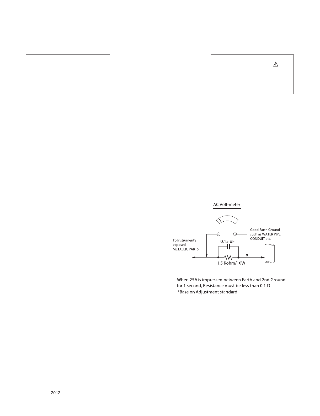
Leakage Current Hot Check (See below Figure)
Plug the AC cord directly into the AC outlet.
Do not use a line Isolation Transformer during this check.
Connect 1.5 K / 10 watt resistor in parallel with a 0.15 uF capacitor
between a known good earth ground (Water Pipe, Conduit, etc.)
and the exposed metallic parts.
Measure the AC voltage across the resistor using AC voltmeter
with 1000 ohms/volt or more sensitivity.
Reverse plug the AC cord into the AC outlet and repeat AC voltage
measurements for each exp ose d metallic par t. Any voltage
measured must not exceed 0.75 volt RMS which is corresponds to
0.5 mA.
In case any measurement is out of the limits specified, there is
possibility of shock hazard and the set must be checked and
repaired before it is returned to the customer.
Leakage Current Hot Check circuit
Only for training and service purposes
- 3 -
LGE Internal Use OnlyCopyright © LG Electronics. Inc. All rights reserved.
Page 4

SERVICING PRECAUTIONS
CAUTION: Before servicing receivers covered by this service
manual and its supplements and addenda, read and follow the
SAFETY PRECAUTIONS on page 3 of this publication.
NOTE: If unforeseen circumstances create conict between the
following servicing precautions and any of the safety precautions
on page 3 of this publication, always follow the safety precautions.
Remember: Safety First.
General Servicing Precautions
1. Always unplug the receiver AC power cord from the AC power
source before;
a. Removing or reinstalling any component, circuit board mod-
ule or any other receiver assembly.
b. Disconnecting or reconnecting any receiver electrical plug or
other electrical connection.
c. Connecting a test substitute in parallel with an electrolytic
capacitor in the receiver.
CAUTION: A wrong part substitution or incorrect polarity
installation of electrolytic capacitors may result in an explosion hazard.
2. Test high voltage only by measuring it with an appropriate
high voltage meter or other voltage measuring device (DVM,
FETVOM, etc) equipped with a suitable high voltage probe.
Do not test high voltage by "drawing an arc".
3. Do not spray chemicals on or near this receiver or any of its
assemblies.
4. Unless specied otherwise in this service manual, clean
electrical contacts only by applying the following mixture to the
contacts with a pipe cleaner, cotton-tipped stick or comparable
non-abrasive applicator; 10 % (by volume) Acetone and 90 %
(by volume) isopropyl alcohol (90 % - 99 % strength)
CAUTION: This is a ammable mixture.
Unless specied otherwise in this service manual, lubrication of
contacts in not required.
5. Do not defeat any plug/socket B+ voltage interlocks with which
receivers covered by this service manual might be equipped.
6. Do not apply AC power to this instrument and/or any of its
electrical assemblies unless all solid-state device heat sinks are
correctly installed.
7. Always connect the test receiver ground lead to the receiver
chassis ground before connecting the test receiver positive
lead.
Always remove the test receiver ground lead last.
8. Use with this receiver only the test xtures specied in this
service manual.
CAUTION: Do not connect the test xture ground strap to any
heat sink in this receiver.
Electrostatically Sensitive (ES) Devices
Some semiconductor (solid-state) devices can be damaged easily by static electricity. Such components commonly are called
Electrostatically Sensitive (ES) Devices. Examples of typical ES
devices are integrated circuits and some eld-effect transistors
and semiconductor “chip” components. The following techniques
should be used to help reduce the incidence of component damage caused by static by static electricity.
1. Immediately before handling any semiconductor component or
semiconductor-equipped assembly, drain off any electrostatic
charge on your body by touching a known earth ground. Alternatively, obtain and wear a commercially available discharging
wrist strap device, which should be removed to prevent potential shock reasons prior to applying power to the unit under test.
2. After removing an electrical assembly equipped with ES
devices, place the assembly on a conductive surface such as
aluminum foil, to prevent electrostatic charge buildup or exposure of the assembly.
3. Use only a grounded-tip soldering iron to solder or unsolder ES
devices.
4. Use only an anti-static type solder removal device. Some solder
removal devices not classied as “anti-static” can generate
electrical charges sufcient to damage ES devices.
5. Do not use freon-propelled chemicals. These can generate
electrical charges sufcient to damage ES devices.
6. Do not remove a replacement ES device from its protective
package until immediately before you are ready to install it.
(Most replacement ES devices are packaged with leads electrically shorted together by conductive foam, aluminum foil or
comparable conductive material).
7. Immediately before removing the protective material from the
leads of a replacement ES device, touch the protective material
to the chassis or circuit assembly into which the device will be
installed.
CAUTION: Be sure no power is applied to the chassis or circuit,
and observe all other safety precautions.
8. Minimize bodily motions when handling unpackaged replacement ES devices. (Otherwise harmless motion such as the
brushing together of your clothes fabric or the lifting of your
foot from a carpeted oor can generate static electricity sufcient to damage an ES device.)
General Soldering Guidelines
1. Use a grounded-tip, low-wattage soldering iron and appropriate
tip size and shape that will maintain tip temperature within the
range or 500 °F to 600 °F.
2. Use an appropriate gauge of RMA resin-core solder composed
of 60 parts tin/40 parts lead.
3. Keep the soldering iron tip clean and well tinned.
4. Thoroughly clean the surfaces to be soldered. Use a mall wirebristle (0.5 inch, or 1.25 cm) brush with a metal handle.
Do not use freon-propelled spray-on cleaners.
5. Use the following unsoldering technique
a. Allow the soldering iron tip to reach normal temperature.
(500 °F to 600 °F)
b. Heat the component lead until the solder melts.
c. Quickly draw the melted solder with an anti-static, suction-
type solder removal device or with solder braid.
CAUTION: Work quickly to avoid overheating the circuit
board printed foil.
6. Use the following soldering technique.
a. Allow the soldering iron tip to reach a normal temperature
(500 °F to 600 °F)
b. First, hold the soldering iron tip and solder the strand against
the component lead until the solder melts.
c. Quickly move the soldering iron tip to the junction of the
component lead and the printed circuit foil, and hold it there
only until the solder ows onto and around both the component lead and the foil.
CAUTION: Work quickly to avoid overheating the circuit
board printed foil.
d. Closely inspect the solder area and remove any excess or
splashed solder with a small wire-bristle brush.
Only for training and service purposes
- 4 -
LGE Internal Use OnlyCopyright © LG Electronics. Inc. All rights reserved.
Page 5

IC Remove/Replacement
Some chassis circuit boards have slotted holes (oblong) through
which the IC leads are inserted and then bent at against the circuit foil. When holes are the slotted type, the following technique
should be used to remove and replace the IC. When working with
boards using the familiar round hole, use the standard technique
as outlined in paragraphs 5 and 6 above.
Removal
1. Desolder and straighten each IC lead in one operation by
gently prying up on the lead with the soldering iron tip as the
solder melts.
2. Draw away the melted solder with an anti-static suction-type
solder removal device (or with solder braid) before removing
the IC.
Replacement
1. Carefully insert the replacement IC in the circuit board.
2. Carefully bend each IC lead against the circuit foil pad and
solder it.
3. Clean the soldered areas with a small wire-bristle brush.
(It is not necessary to reapply acrylic coating to the areas).
"Small-Signal" Discrete Transistor
Removal/Replacement
1. Remove the defective transistor by clipping its leads as close
as possible to the component body.
2. Bend into a "U" shape the end of each of three leads remaining
on the circuit board.
3. Bend into a "U" shape the replacement transistor leads.
4. Connect the replacement transistor leads to the corresponding
leads extending from the circuit board and crimp the "U" with
long nose pliers to insure metal to metal contact then solder
each connection.
Power Output, Transistor Device
Removal/Replacement
1. Heat and remove all solder from around the transistor leads.
2. Remove the heat sink mounting screw (if so equipped).
3. Carefully remove the transistor from the heat sink of the circuit
board.
4. Insert new transistor in the circuit board.
5. Solder each transistor lead, and clip off excess lead.
6. Replace heat sink.
Diode Removal/Replacement
1. Remove defective diode by clipping its leads as close as possible to diode body.
2. Bend the two remaining leads perpendicular y to the circuit
board.
3. Observing diode polarity, wrap each lead of the new diode
around the corresponding lead on the circuit board.
4. Securely crimp each connection and solder it.
5. Inspect (on the circuit board copper side) the solder joints of
the two "original" leads. If they are not shiny, reheat them and if
necessary, apply additional solder.
3. Solder the connections.
CAUTION: Maintain original spacing between the replaced
component and adjacent components and the circuit board to
prevent excessive component temperatures.
Circuit Board Foil Repair
Excessive heat applied to the copper foil of any printed circuit
board will weaken the adhesive that bonds the foil to the circuit
board causing the foil to separate from or "lift-off" the board. The
following guidelines and procedures should be followed whenever
this condition is encountered.
At IC Connections
To repair a defective copper pattern at IC connections use the
following procedure to install a jumper wire on the copper pattern
side of the circuit board. (Use this technique only on IC connections).
1. Carefully remove the damaged copper pattern with a sharp
knife. (Remove only as much copper as absolutely necessary).
2. carefully scratch away the solder resist and acrylic coating (if
used) from the end of the remaining copper pattern.
3. Bend a small "U" in one end of a small gauge jumper wire and
carefully crimp it around the IC pin. Solder the IC connection.
4. Route the jumper wire along the path of the out-away copper
pattern and let it overlap the previously scraped end of the
good copper pattern. Solder the overlapped area and clip off
any excess jumper wire.
At Other Connections
Use the following technique to repair the defective copper pattern
at connections other than IC Pins. This technique involves the
installation of a jumper wire on the component side of the circuit
board.
1. Remove the defective copper pattern with a sharp knife.
Remove at least 1/4 inch of copper, to ensure that a hazardous
condition will not exist if the jumper wire opens.
2. Trace along the copper pattern from both sides of the pattern
break and locate the nearest component that is directly connected to the affected copper pattern.
3. Connect insulated 20-gauge jumper wire from the lead of the
nearest component on one side of the pattern break to the lead
of the nearest component on the other side.
Carefully crimp and solder the connections.
CAUTION: Be sure the insulated jumper wire is dressed so the
it does not touch components or sharp edges.
Fuse and Conventional Resistor
Removal/Replacement
1. Clip each fuse or resistor lead at top of the circuit board hollow
stake.
2. Securely crimp the leads of replacement component around
notch at stake top.
Only for training and service purposes
- 5 -
LGE Internal Use OnlyCopyright © LG Electronics. Inc. All rights reserved.
Page 6
SPECIFICATION
NOTE : Specifications and others are subject to change without notice for improvement
.
1. Application range
This specification is applied to the LCD TV used LC22E
chassis.
2. Requirement for Test
Each part is tested as below without special appointment.
1) Temperature: 25 °C ± 5 °C(77 °F ± 9 °F), CST: 40 °C ± 5 °C
2) Relative Humidity: 65 % ± 10 %
3) Power Voltage
: Standard input voltage (AC 100-240 V~, 50/60 Hz)
* Standard Voltage of each products is marked by models.
4) Specification and performance of each parts are followed
each drawing and specification by part number in
accordance with BOM.
5) The receiver must be operated for about 20 minutes prior to
the adjustment.
3. Test method
1) Performance: LGE TV test method followed
2) Demanded other specification
- Safety : CE, IEC specification
- EMC : CE, IEC
- Wireless : Wireless HD Specification (Option)
4. Model General Specification
No. Item Remarks
1. Market
2. Broadcasting system
3.
Receiving system
CHINA , HONG KONG
(PAL/DVB Market)
1) PAL/SECAM-B/G/D/K
2) PAL-I/II
3) NTSC-M
4) DVB-T
Analog : Upper Heterodyne
Digital : COFDM(DVB-T)
► DTMB
( Carrier , Code Rate , Constellation , Frame Header ,
Interleaving )*. China
- MODE1 : 3780 , 0.4 , 16QAM , PN945 , 720 , 9.626Mbps
- MODE2 : 1 , 0.8 , 4QAM , PN595 , 720 , 10.396Mbps
- MODE3 : 3780 , 0.6 , 16QAM , PN945 , 720 , 14.438Mbps
- MODE4 : 1 , 0.8 , 16QAM , PN595 , 720 , 20.791Mbps
- MODE5 : 3780 , 0.8 , 16QAM , PN420 , 720 , 21.658Mbps
- MODE6 : 3780 , 0.6 , 64QAM , PN420 , 720 , 24.365Mbps
- MODE7 : 1 , 0.8 , 32QAM , PN595 , 720 , 25.989Mbps
*. HONG KONG
- MODE : 3780 , 0.4/0.6 , 4/16/64QAM , PN945 , 720
QPSK : 1/2, 2/3, 3/4, 5/6, 7/8
16-QAM : 1/2, 2/3, 3/4, 5/6, 7/8
64-QAM : 1/2, 2/3, 3/4, 5/6, 7/8
► DVB-C
- Symbolrate :
4.0Msymbols/s to 7.2Msymbols/s
- Modulation :
16QAM, 64-QAM, 128-QAM and 256-QAM
4 Video Input RCA(1EA)
5. Component Input Y/Cb/Cr, Y/Pb/Pr
6. RGB Input RGB-PC Analog(D-SUB 15PIN)
7. HDMI Input
8. Audio Input
9. SPDIF out SPDIF out
10 USB Input
11 Lan Jack
HDMI1-DTV/DVI,HDMI2-DTV/DVI
HDMI3-DTV/DVI,HDMI4-DTV/DVI
Component
RGB/DVI Audio
FEMF, DivX HD, For SVC (download)
AV
AV gender jack 1EA
PC(HDMI version 1.3)
Support HDCP
L/R Input
JPEG, MP3, DivX HD
- 6 -
Only for training and service purposes
LGE Internal Use OnlyCopyright © LG Electronics. Inc. All rights reserved.
Page 7
5. Component Video Input (Y, Cb/Pb, Cr/Pr)
No. Resolution H-freq(kHz) V-freq(Hz) Porposed
1 720×480 15.73 60.00 SDTV, DVD 480i
2 720×480 15.63 59.94 SDTV, DVD 480i
3 720×480 31.47 59.94 480p
4 720×480 31.50 60.00 480p
5 720×576 15.625 50.00 SDTV, DVD 625 Line
6 720×576 31.25 50.00 HDTV 576p
7 1280×720 45.00 50.00 HDTV 720p
8 1280×720 44.96 59.94 HDTV 720p
9 1280×720 45.00 60.00 HDTV 720p
10 1920×1080 31.25 50.00 HDTV 1080i
11 1920×1080 33.75 60.00 HDTV 1080i
12 1920×1080 33.72 59.94 HDTV 1080i
13 1920×1080 56.250 50 HDTV 1080p
14 1920×1080 67.5 60 HDTV 1080p
6. RGB input (PC)
No. Resolution H-freq(kHz) V-freq.(Hz) Proposed Remark
720*400 31.468 70.08 VESA(VGA) For only DOS mode
1
640*480 31.469 59.94 VESA(SVGA)
2
800*600 37.879 60.31 VESA(XGA)
3
1024*768 48.363 60.00 VESA
4
1360*768 47.72 59.8 VESA(WXGA)
5
1920*1080 66.587 59.93
6
WUXGA(CEA 861D)
Input 848*480 60Hz,
852*480 60Hz
->640*480 60Hz Display
FHD only
Only for training and service purposes
- 7 -
LGE Internal Use OnlyCopyright © LG Electronics. Inc. All rights reserved.
Page 8
7. HDMI Input
7.1. DTV mode
No. Resolution H-freq(kHz) V-freq.(kHz) Proposed Proposed
1. 720*480 31.469 / 31.5 59.94 / 60 27.00/27.03 SDTV 480P
2. 720*576 31.25 50 54 SDTV 576P
3. 1280*720 37.500 50 74.25 HDTV 720P
4. 1280*720 44.96 / 45 59.94 / 60 74.17/74.25 HDTV 720P
5. 1920*1080 33.72 / 33.75 59.94 / 60 74.17/74.25 HDTV 1080I
6. 1920*1080 28.125 50.00 74.25 HDTV 1080I
7. 1920*1080 26.97 / 27 23.97 / 24 74.17/74.25 HDTV 1080P
8. 1920*1080 33.716/ 33.75 29.976/30.00 74.25 HDTV 1080P
9. 1920*1080 56.250 50 148.5 HDTV 1080P
10. 1920*1080 67.43 / 67.5 59.94 / 60 148.35/148.50 HDTV 1080P
7.2. PC mode
No. Resolution H-freq(kHz) V-freq.(Hz) Proposed Remark
1 31.468 70.08
720 x 400
2
640 x 480
3
800 x 600
1024 x 768
4
5
1360 x 768
1280 x 1024
6 63.595 60.0
1920 x 1080 67.5
7
31.469 59.94 VESA
37.879 60.31 VESA
48.363
47.712 59.8
60.00
60.0
VESA(XGA)
WXGA
SXGA
WUXGA
HDCP
HDCP
HDCP
HDCP
HDCP
HDCP / FHD model
HDCP / FHD model
Only for training and service purposes
- 8 -
LGE Internal Use OnlyCopyright © LG Electronics. Inc. All rights reserved.
Page 9

ADJUSTMENT INSTRUCTION
Caution) When still image is displayed for a period of 20
minutes or longer (especially where W/B scale is strong.
Digital pattern 13ch and/or Cross hatch pattern 09ch),
there can some afterimage in the black level area.
1. Application Range
This specification sheet is applied to all of the LED LCD TV
with LC22E chassis.
2. Designation
(1) ecause this is not a hot chassis, it is not necessary to
use an isolation transformer. However, the use of
isolation transformer will help protect test instrument.
(2) Adjustment must be done in the correct order.
(3) The adjustment must be performed in the circumstance of
25 ±5 C of temperature and 65±10% of relative humidity if
there is no specific designation.
(4) The input voltage of the receiver must keep 100~240V, 50/60Hz.
(5) The receiver must be operated for about 5 minutes prior to
the adjustment when module is in the circumstance of over 15.
In case of keeping module is in the circumstance of 0 °C, it
should be placed in the circumstance of above 15 °C for 2
hours
In case of keeping module is in the circumstance of below -20
°C, it should be placed in the circumstance of above 15 °C for
3 hours.
3.3. Etc
▪Ship-out mode
▪Service Option Default
▪USB Download(S/W Update, Option, Service only)
▪ISP Download(Option)
4.Automatic Adjustment
■ Enter Service Mode by pushing “ADJ” key,
■ Enter ADC mode by pushing “► key at “8. ADC Calibration”
■ There are 2 ways for ADC Calibration. ( OTP, External )
*. OTP mode
: Automatic ADC Calibration. (Internal ADC Calibration) On the
manufacture line, OTP is used for ADC Calibration automatically.
*. External mode
: Manual ADC Calibration. When OTP mode is failed, ADC
calibration should be “OK” by using External mode.
4.1. Final assembly adjustment
1. Change the ADC type “OTP” by using “►”key.
2. Enter “Start” key.
3. Check the sign “OK” below ADC type.
3. Adjustment items
3.1 Main PCB check process
▪MAC Address Download
▪Wide-Vine Key Download
▪Adjust 1920*1080 Comp1
▪Adjust 1920*1080 RGB
▪EDID/DDC download
Above adjustment items can be also performed in
Final Assembly if needed. Both Board-level and
Final assembly adjustment items can be check
using In-Start Menu.
1.ADJUST CHECK.
3.2. Final assembly adjustment
▪White Balance adjustment
▪RS-232C functionality check
▪ PING Test
▪Factory Option setting per destination
▪Ship-out mode setting (In-Stop)
4.1.2 External ADC Adjustment
Overview
ADC adjustment is needed to find the optimum black level and gain
in Analog-to-Digital device and to compensate RGB deviation.
Equipment & Condition
1) USB to RS-232C Jig
2) MSPG-925 Series Pattern Generator(MSPG-925FA, pattern -65)
- Resolution: 1080P Comp1
1920*1080P RGB
- Pattern : Horizontal 100% Color Bar Pattern
- Pattern level : 0.7±0.1 Vp-p
- Image
Adjustment method
▪ Using USB, adjust items listed in 3.1 in the other shown in “4.1.3.3”
Only for training and service purposes
- 9 -
LGE Internal Use OnlyCopyright © LG Electronics. Inc. All rights reserved.
Page 10
Adj. protocol
Protocol
Command
Set ACK
Enter adj. mode
aa 00 00
a 00 OK00x
Source change
xb 00 04
xb 00 06
b 00 OK04x (Adjust 480i, 1080p Comp1 )
b 00 OK06x (Ad
just 1920*1080 RGB)
Begin adj.
ad 00 10
Return adj. result
OKx (Case of Success)
NGx (Case of Fail)
Read adj. data
(main)
ad 00 20
(sub )
ad 00 21
(main)
000000000000000000000000007c007b006dx
(Sub)
000000070000000000000000007c00830077x
Confirm adj
.
ad 00 99
NG 03 00x (Fail)
NG 03 01x (Fail)
NG 03 02x (Fail)
OK 03 03x (Success)
End adj.
aa 00 90
a 00 OK90x
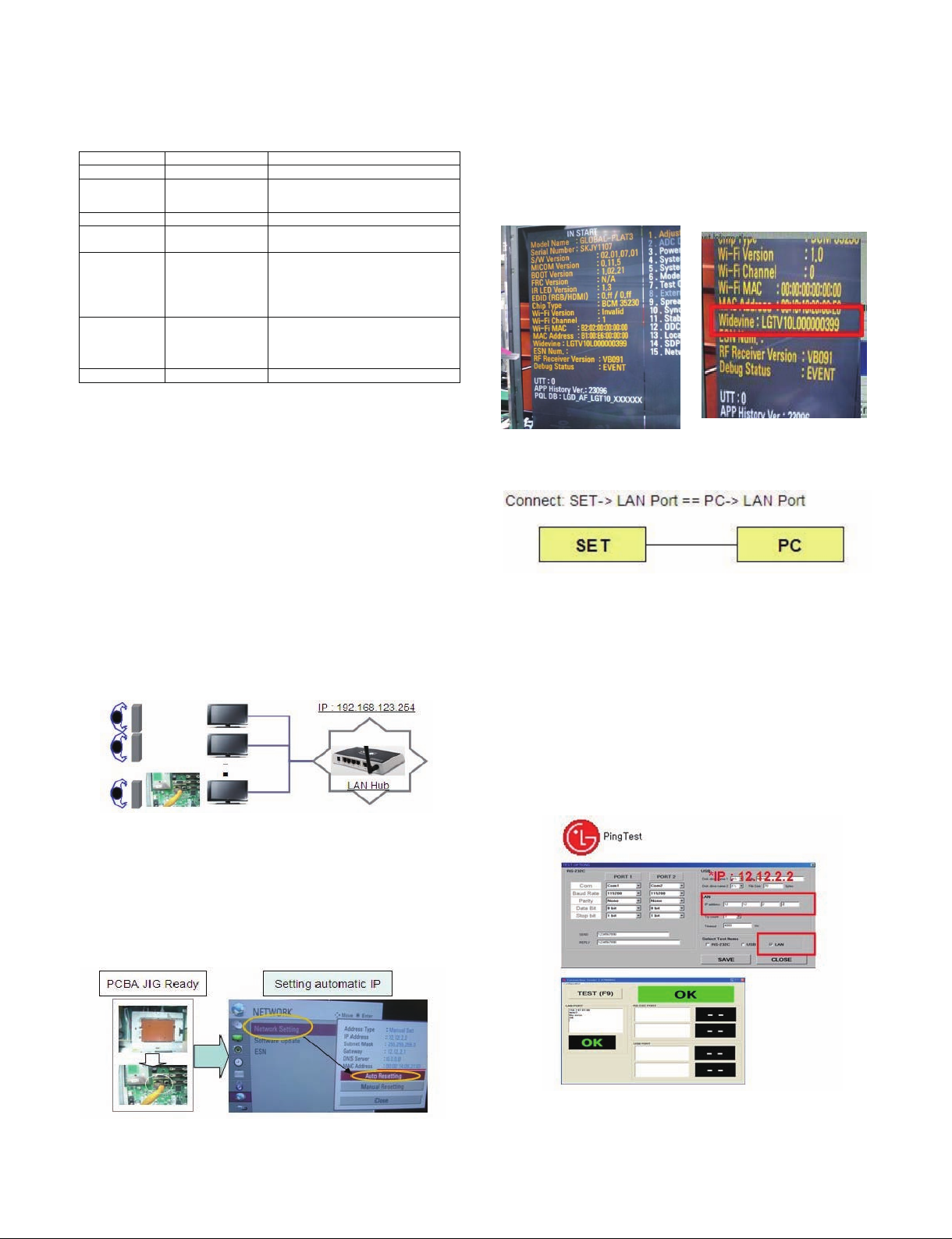
4.2.3 WIDEVINE Key Inspection
Ref.) ADC Adj. RS232C Protocol_Ver1.0
Adj. order
▪aa 00 00 [Enter ADC adj. mode]
▪xb 00 04 [Change input source to Component1(480i&1080p)]
▪ad 00 10 [Adjust 480i&1080p Comp1]
▪xb 00 06 [Change input source to RGB(1024*768)]
▪ad 00 10 [Adjust 1920*1080 RGB]
▪aa 00 90 End adj.
. WIDEVINE Key Inspection
- Confirm Key input Data at the “IN START” MENU Mode
4.3 LAN PORT INSPECTION(PING TEST)
Ref) ADC adj. RS232C Protocol_Ver1.0
4.2 LAN Inspection
4.2.1 Equipment & Condition
▪ Each other connection to LAN Port of IP Hub and Jig。
4.2.2 LAN inspection solution
LAN Port connection with PCB
▪ Network setting at MENU Mode of TV
▪ setting automatic IP
▪ Setting state confirmation
If automatic setting is finished, you confirm IP and MAC Address.
Only for training and service purposes
4.4.1. Equipment setting
1) Play the LAN Port Test PROGRAM.
2) Input IP set up for an inspection to Test
Program.
*IP Number : 12.12.2.2
4.4.2. LAN PORT inspection (PING TEST)
1) Play the LAN Port Test Program.
2) connect each other LAN Port Jack.
3) Play Test (F9) button and confirm OK Message.
4) remove LAN CABLE
- 10 -
LGE Internal Use OnlyCopyright © LG Electronics. Inc. All rights reserved.
Page 11
4.3 Model name & Serial number
Command
Set ACK
T
ransmission
[A][l][][Set ID][][20][Cr]
[O][K][x] or [N][G]
For Analog EDID For HDMI EDID
D-sub to D-sub
DVI-D to HDMI or HDMI to HDMI
Download
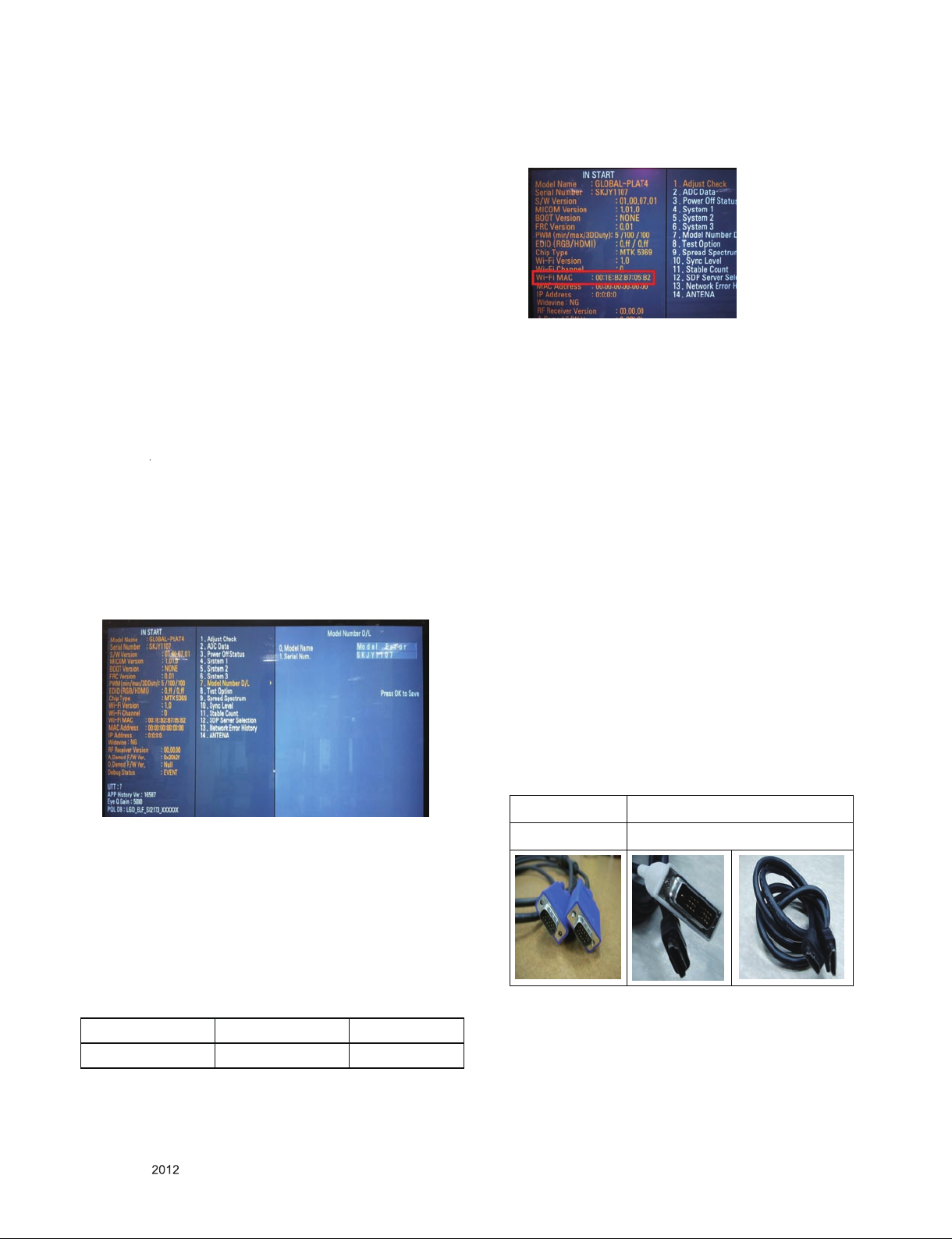
4.3.1 Model name & Serial number D/L
■ Press “Power on” key of service remocon.(Baud rate :
115200 bps)
■ Connect RS-232C Signal to USB Cable to USB.
■ Write Serial number by use USB port.
■ Must check the serial number at Instart menu.
b. check the menu on in-start
4.3.2 Method & notice
A. Serial number D/L is using of scan equipment.
B. Setting of scan equipment operated by Manufacturing
Technology Group.
C. Serial number D/L must be conformed when it is produced in
production line, because serial number D/L is mandatory by
D-book 4.0
* Manual Download (Model Name and Serial Number)
If the TV set is downloaded By OTA or Service man,
Sometimes model name or serial number is initialized.( Not always)
There is impossible to download by bar code scan, so It need
Manual download.
a. Press the ‘instart’ key of ADJ remote controller.
b. Go to the menu ‘5.Model Number D/L’ like below photo.
c. Input the Factory model name(ex 47LM6200-CC) or Serial
number like photo.
5. Manual Adjustment
5.1. ADC adjustment is not needed because\
of OTP(Auto ADC adjustment)
5.2. EDID (The Extended Display Identification Data) / DDC (Display Data Channel)
download
5.2.1 Overview
It is a VESA regulation. A PC or a MNT will display an optimal
resolution through information sharing without any
necessity of user input. It is a realization of “Plug and Play”.
5.2.2 Equipment
▪ Since embedded EDID data is used, EDID download JIG,
HDMI cable and D-sub cable are not need.
▪ Adjust remocon
5.2.3 Download method
1) Press Adj. key on the Adj. R/C, then select “12.EDID D/L”.
By pressing Enter key, enter EDID D/L menu.
2) Select [Start] button by pressing Enter key, HDMI1 / HDMI2 / HDMI3
/ HDMI4 / RGB are Writing and display OK or NG.
d. Check the model name Instart menu -->Factory name displayed
(ex 47LM62000-CA)
e. Check the Diagnostics (DTV country only) --> Buyer model
displayed (ex 47LM6200-CC)
4.4 WIFI MAC ADDRESS CHECK
a. Using RS232 Command
Only for training and service purposes
- 11 -
LGE Internal Use OnlyCopyright © LG Electronics. Inc. All rights reserved.
Page 12
RGB_EDID DATA *Vendor Specific(HDMI)DATA
HEX
EDID Table
DDC
Function
0001
0100
Analog
0001
0100
Digital
Chassis
MODEL NAME(HEX)
LD22E
00 00 00 FC 00 4C 47 20 54 56 0A 20 20 20 20 20 20 20 20
ⓔ1
ⓔ2
ⓔ3
HDMI1
9D
49
X
HDMI2
9D
39
X
HDMI3
9D
29
X
HDMI4
9D
19
X
RGB X X
80
INPUT
MODEL NAME(HEX)
HDMI1
78 03 0C 00 10 00 B8 2D 20 C0 0E 01 40 0A 3C 08 10 18 10 98 10 58 10 38 10
HDMI2
78 03 0C 00 20 00 B8 2D 20 C0 0E 01 40 0A 3C 08 10 18 10 98 10 58 10 38 10
HDMI3
78 03 0C 00 30 00 B8 2D 20 C0 0E 01 40 0A 3C 08 10 18 10 98 10 58 10 38 10
HDMI4
78 03 0C 00 40 00 B8 2D 20 C0 0E 01 40 0A 3C 08 10 18 10 98 10 58 10 38 10
Color Analyzer
Computer
Pattern Generator
※
※If TV internal pattern is used, not needed
Signal Source
Probe
RS-232C
RS-232C
USB to RS-232C
0x00 0x 01 0x0 2 0x 03 0 x04 0 x05 0 x06 0x07 0x08 0x0 9 0x0A 0x0B 0x 0C 0x0D 0x 0E 0x0 F
0x00 00 FF FF FF FF FF FF 00 1E 6D a b
0x01 c 01 03 68 A0 5A 78 0A EE 91 A3 54 4 C 99 26
0x02 0F 50 54 A1 08 00 31 40 4 5 40 61 40 71 40 81 80
0x03 01 01 01 01 01 01 02 3A 80 18 71 38 2D 40 5 8 2C
0x04 45 00 A0 5 A 00 00 00 1E 66 21 5 0 B0 51 00 1B 30
0x05 40 70 36 0 0 A0 5A 00 0 0 00 1E 00 00 00 FD 00 3A
0x06 3E 1E 53 10 00 0A 20 20 2 0 20 2 0 20 d
0x07 d 00 e3
5.3 White Balance Adjustment
5.2.4 EDID DATA
▪Reference
- HDMI1 ~ HDMI4 / RGB
- In the data of EDID, bellows may be different by S/W or Input mode.
*Product ID
Serial No: Controlled on production line.
*Month, Year: Controlled on production line: ex)
Monthly : ‘01’ -〉 ‘01’
3D FHD RGB EDID data
0x00 0x 01 0x0 2 0x 03 0 x04 0 x05 0 x06 0x07 0x08 0x0 9 0x0A 0x0B 0x 0C 0x0D 0x 0E 0x0 F
0x00 00 FF FF FF FF FF FF 00 1E 6D a b
0x01 c 01 03 8 0 A0 5A 78 0A EE 91 A3 54 4 C 99 26
0x02 0F 50 54 A1 08 00 31 40 4 5 40 61 40 71 40 81 80
0x03 01 01 01 01 01 01 02 3A 80 18 71 38 2D 40 5 8 2C
0x04 45 00 A0 5 A 00 00 00 1E 66 21 5 0 B0 51 00 1B 30
0x05 40 70 36 0 0 A0 5A 00 0 0 00 1E 00 00 00 FD 00 3A
0x06 3E 1E 53 10 00 0A 20 20 2 0 20 2 0 20 d
0x07 d 01 e1
0x00 02 03
0x01 22 15 01 26 15 07 50 09 57 07 f
0x02 f
0x03 f E3 05 03 01 02 3A 80 18 71 38 2D 40 58
0x04 2C 45 00 A0 5A 00 00 00 1E 01 1D 80 18 71 1C 16
0x05 20 58 2C 25 00 A0 5A 00 00 00 9E 01 1D 00 7 2 51
0x06 D0
0x07 00 00 00 00 00 00 00 00 00 00 00 00 00 00 00 e2
37 F1 4E 10 9F 04 13 05 14 03 02 12 20 21
1E 20 6E 28 55 00 A0 5A 00 00 00 1E 00 00 00
5.3.1 Overview
▪ W/B adj. Objective & How-it-works
- Objective: To reduce each Panel’s W/B deviation
- How-it-works: When R/G/B gain in the OSD is at 192, it means the
panel is at its Full Dynamic Range. In order to prevent saturation
of Full Dynamic range and data, one of R/G/B is fixed at 192, and the
other two is lowered to find the desired value.
-Adj. condition : normal temperature
2) Warm-up time: About 5 Min
3) Surrounding Humidity: 20% ~ 80%
5.3.2 Equipment
1) Color Analyzer: CA-210 (LED Module : CH 14)
2) Adj. Computer(During auto adj., RS-232C protocol is needed)
3) Adjust Remocon
4) Video Signal Generator MSPG-925F 720p/204-Gray(Model:217,
Pattern:49)
→ Only when internal pattern is not available
▪Color Analyzer Matrix should be calibrated using CS-100。
5.3.3 Equipment connection MAP
*Model Name(Hex): LGTV
*Checksum(LG TV): Changeable by total EDID data.
Only for training and service purposes
5.3.4 Adj. Command (Protocol)
<Command Format>
START 6E A 50 A LEN A 03 A CMD A 00 A VAL A CS A STOP
- LEN: Number of Data Byte to be sent
- CMD: Command
- VAL: FOS Data value
- CS: Checksum of sent data
- A: Acknowledge
Ex) [Send: JA_00_DD] / [Ack: A_00_okDDX]
▪RS-232C Command used during auto-adj.
- 12 -
LGE Internal Use OnlyCopyright © LG Electronics. Inc. All rights reserved.
Page 13
5.4 EYE-Q function check
Aging time
Cool
Medium
Warm
(Min) x y x y x y
GP4
269
273
285
293
313
329
1
0-2
283
293
299
313
320
339
2
3-5
282
291
298
311
319
337
3
6-9
281
290
297
310
318
336
4
10-19
279
289
295
309
316
335
5
20-35
277
284
293
304
314
330
6
36-49
274
279
290
299
311
325
7
50-79
271
277
287
297
308
323
8
80-119
270
274
286
294
307
320
9
Over 120
269
273
285
293
306
319
-equipment : RF Remocon for test, IR-KEY-Code Remocon for test
-You must confirm the battery power of RF-Remocon before test
(recommend that change the battery per every lot)
-Sequence (test)
a)if you select the ‘start key(OK)’ on the controller, you can
pairing with the TV SET.
b)You can check the cursor on the TV Screen, when select the
‘OK Key’ on the controller
c) You must remove the pairing with the TV Set by
‘Mute + OK Key’ on the controller。
5.7 3D function test
Step 1) Turn on TV
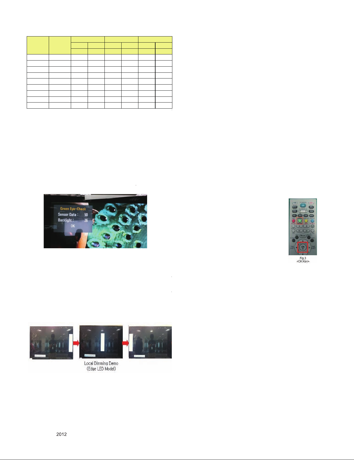
Step 2) Press EYE key of Adj. R/C
Step 3) Cover the Eye Q II sensor on the front of the using your hand
and wait for 6 seconds
Step 4) Confirm that R/G/B value is lower than 10 of the “Raw Data
(Sensor data, Back light )” . If after 6 seconds, R/G/B value is
not lower than 10, replace Eye Q II sensor
Step 5) Remove your hand from the Eye Q II sensor and wait for 6
seconds
Step 6) Confirm that “ok” pop up. s
If change is not seen, replace Eye Q II sensor
5.5 Local Dimming Function Check
Step 1) Turn on TV
Step 2) At the Local Dimming mode, module Edge Backlight moving
right to left
Back light of IOP module moving
Step 3) confirm the Local Dimming mode
Step 4) Press “exit” Key.
(Pattern Generator MSHG-600, MSPG-6100 [SUPPORT HDMI1.4])
* HDMI mode NO. 872 , pattern No.83
1) Please input 3D test pattern like below
(HDMI mode NO. 872 , pattern No.83)
2.When 3D OSD appear automatically ,
then select green button.
3. Don’t wear a 3D Glasses,
Check the picture like below .
5.6 Magic Motion Remocon test
Only for training and service purposes
5.8 3D Depth function TEST
5.9 Wi-Fi Test(LM6200 not support
Wi-Fi)
5.10 LNB voltage and 22KHz tone
check (only for DVB-S/S2 model)
Test method
- 13 -
LGE Internal Use OnlyCopyright © LG Electronics. Inc. All rights reserved.
Page 14
1. Set TV in Adj. mode using POWER ON.
2. Connect cable between satellite ANT and test JIG.
4. Press Yellow Key (ETC+SWAP) in Adj Remocon to make LNB on.
5. check LED light ‘ON’ at 18V menu.
6. check LED light ‘ON’ at 22KHz tone menu.
7. Press Blue Key (ETC+PIP INPUT) in Adj Remocon to make LNB off.
8. check LED light ‘OFF’ at 18V menu.
9. check LED light ‘OFF’ at 22KHz tone menu.
Test result
1. After press LNB On key, ‘18V LED’ and ‘22KHz tone LED’ should be
ON.
2. After press LNB OFF key, ‘18V LED’ and ‘22KHz tone LED’ should
be OFF.
6.2.2 Checkpoint
▪ TEST voltage
- GND: 1.5KV/min at 100mA
- SIGNAL: 3KV/min at 100mA
▪ TEST time: 1 second
▪ TEST POINT
- GND TEST = POWER CORD GND & SIGNAL CABLE METAL GND
- Internal Pressure TEST = POWER CORD GND & LIVE & NEUTRAL
▪ LEAKAGE CURRENT: At 0.5mArms.
7. Audio
5.11 Option selection per country
5.11.1 Overview
▪ Option selection is only done for models in Non-EU
5.11.2 Method
1) Press ADJ key on the Adj. R/C, then select Country Group Meun
2) Depending on destination, select Country Group Code 04 or
Country Group EU then on the lower Country option, select US, CA,
6.0 Tool Option selection
Method: Press Adj. key on the Adj. R/C, then select Tool option.
▪
6.1 Ship-out mode check (In-stop)
▪ After final inspection, press In-Stop key of the Adj. R/C and check
that the unit goes to Stand-by mode.
6.2 GND and Internal Pressure check
6.2.1 Method
1) GND & Internal Pressure auto-check preparation
- Check that Power Cord is fully inserted to the SET.
(If loose, re-insert)
2) Perform GND & Internal Pressure auto-check
- Unit fully inserted Power cord, Antenna cable and A/V arrive to
the auto-check process.
- Connect D-terminal to AV JACK TESTER
- Auto CONTROLLER(GWS103-4) ON
- Perform GND TEST
- If NG, Buzzer will sound to inform the operator.
- If OK, changeover to I/P check automatically.
(Remove CORD, A/V form AV JACK BOX)
- Perform I/P test
- If NG, Buzzer will sound to inform the operator.
- If OK, Good lamp will lit up and the stopper will allow the pallet to
move on to next process.
No Item Min Typ Max Unit Remark
No
1.
Audio practical max
1
Output, L/R
(Distortion=10%
max Output)
2.
Speaker (8Ω
Impedance)
9 10 12 W
8.10 10.8 Vrms
10 12 W EQ On
AVL Off
Clear Voice Off
AVL On
Clear Voice On
EQ Off
Measurement condition:
1. RF input: Mono, 1KHz sine wave signal, 100% Modulation
2. CVBS, Component: 1KHz sine wave signal 0.5Vrms
3. RGB PC: 1KHz sine wave signal 0.7Vrms.
8.1 SET Factoring Condition
No. Item Condition Remark
1.
Power
2. Volume Level 10
3. Main Picture Input
4. Main Last Channel N.A.
5. Mute Off
6. ARC 16:9(DTV)
Energy Saving
3D Settings
7. PICTURE
Picture Mode
Off
DTV
Auto
Standard
Backlight Energy Saving
Contrast 100
Brightness 50
Sharpness 25
Colour 60
Tint 0
Colour Temp 0
DTV&ATV
Only for training and service purposes
- 14-
LGE Internal Use OnlyCopyright © LG Electronics. Inc. All rights reserved.
Page 15
Sound Mode
Standard
Stanard
Music
Cinema
Sport
Game
Vivid
User setting
User EQ
Auto Volume
Off
Volume Mode
Volume Control
Medium
Dynamic EQ
On
Natural Sound
Bass Enhancer
On
Sound Optimizer
Normal
Infinite
Surround
On
Clear Voice II
Off
AV sync.
Off
DTV
Audio Setting
Auto
ARC Mode
Off
Balance
0
TV Speaker
On
8.
AUDIO
Audio Setting
Digital Audio Out
PCM
Auto Tuning
Manual Tuning
DTV/TV
Programme Edit
DTV/Radio/TV
9.
SETUP
(DTV&ATV)
CI information
Module
Clock
-- : --
User control
Off time
Off
On time
Off
Sleep Timer
Off
10.
Time
Automatic
Standby
4 hours
Product/Service
Info.
Initialization of
Premium
Set Password
New * * * *
Confirm * * * *
Off
Block Programme
DTV/RADIO/TV
Parental Guidance
Blocking Off
11.
LOCK
Lock System
Input Block
Menu Language
English
Audio Language
English
Language
Subtitle Language
English
Country
- -
Hard of Hearing
Off
Audio Description
Off
Volume
0
Disability
Assistance
Beep
Off
Stand by Light
On
Power Indicator
Power Light
On
Speed
Normal
Shape
Type D
Size
Medium
Pointer
Alignment
On
Factory Reset
Set ID 1
12.
OPTION
Mode Setting
Home Use
Network
Connection
Network Status
Wi-Fi Direct /
Wi-Fi Screen
13.
Network
Smart Share
Setting
Software Update
Picture Test
Sound Test
14.
SUPPORT
Signal Test
Energy Saving
Auto
3D Settings
Standard
Backlight
Energy Saving
Contrast
100
Brightness
50
Sharpness
25
Colour
60
Tint
0
Colour Temp
0
Dynamic
Contrast
Medium
Dynamic
Colour
Low
Clear White
off
Skin Colour
0
Grass Color
0
Sky Color
0
Noise
Reduction
Low
Super
Resolution
On
MPEG Noise
Reduction
Medium
Gamma
Medium
Black Level
Auto
Eye Care
Low
Real
Cinema
On
Colour
Gamut
Wide
xvYCC
Off
Picture Mode
Picture Reset
7.
PICTURE
Aspect Ratio
16:9
Only for training and service purposes
- 15-
LGE Internal Use OnlyCopyright © LG Electronics. Inc. All rights reserved.
Page 16

8.2 USB S/W Download (option, Service only)
HK (17)
198
41675
17229
37325
23191
1321
13355
1. Put the USB Stick to the USB socket
2. Automatically detecting update file in USB Stick
- If your downloaded program version in USB Stick is Lower, it didn’t work.
But your downloaded version is Higher, USB data is automatically detecting
(Download Version High & Power only mode, Set is automatically Download)
3. Show the message “Copying files from memory
4. Updating is staring.
5. Updating Completed, The TV will restart automatically
6. If your TV is turned on, check your updated version and Tool
option. (explain the Tool option, next stage)
* If downloading version is more high than your TV have, TV
can lost all channel data. In this case, you have to channel
ecover. if all channel data is cleared, you didn’t have a DTV/ATV
test on production line.
* After downloading, have to adjust TOOL OPTION again.
1. Push "IN-START" key in service remote controller.
2. Select "Tool Option 1" and Push “OK” button.
3. Punch in the number. (Each model has their number.)
9.3 Tool Option selection
▪ Method: Press Adj. key on the Adj. R/C, then select Tool option.
Area(Code)
47LM7600-CA
Option1
Option2 Option3 Option4
Option5
Option6
Option7
Only for training and service purposes
- 16-
LGE Internal Use OnlyCopyright © LG Electronics. Inc. All rights reserved.
Page 17

BLOCK DIAGRAM
FPC(51P)
IC1202
DDR3 1Gb
LVDS
X-tal
SERIAL FLASH
(FHD/50Hz)
24M
DDR3 1Gb
MX25L8005M2I
IC1401 (8M bit)
SPI
DDR3 Add.
Rear
SIF
TU_CVBS
FE_TS_DATA[0:7]
IC104 256Kbit
M24M01-HRMN6TP
IC1201
H5TQ1G63BFR
H5TQ1G63BFR
I2C
DDR3 Data
TMDS
CVBS, Y/Pb/Pr, L/R
CI Slot
CI Slot:
Only LM5700 for China
74LCX244
Buffer
FE_TS_DATA[0:7]
CONTROL
IR & LED /
SOFT TOUCH
NAND FLASH
IC102 (2Gbit)
PCM_A[0:7]
IC101
LG2111A
RGB/H/V
Y/Pb/Pr, L/R
TS_DATA[0:7]
PCM_A[8:14]
PCM_DATA[0:7]
KEY1
SENSOR
_SCL/SDA
L/R
SPDIF
EPHY
(TACT SWITCH)
LED_R
IR
KEY2
DP/DM
USB
SPK L/R
Audio AMP
STA380BWE
I2S
TMDS
HDMI3
Only for training and service purposes
Tuner
Tuner
RGB PC
HDMI1/2(DVI)
Component/AV
Component
- 17 -
SPDIF
Ethernet
PC/DVI Audi In
Side
Except of
LM4600/LM3100/
LM3400/LS4100/
LS3500/CS460
LGE Internal Use OnlyCopyright © LG Electronics. Inc. All rights reserved.
Page 18

Intelligent sensor
IR BOARD
HDCP EEPROM
NVRAM
IC103
IC104
100Ω
1KΩ
SENSOR_SCL
SENSOL_SDA
+3.3V_Normal
LGE2111A
22Ω
2.2KΩ
22Ω
I2C_SCL
I2C_SDA
+3.3V_Normal
We can be changed by software
Driving Current : 2/4/6/8mA
configuration.
IC101
AMP_SCL
(DEMOD_SCL)
AMP_SDA
(DEMOD_SDA_
TU_SCL
TU_SDA
+3.3V_Normal
DEMOD_SCL
DEMOD_SDA
AMP_SDA
22Ω
1KΩ
+3.3V_TU
1KΩ
AMP_SCL
33Ω
Only for training and service purposes
TUNER(D.D)
STA380BW
IC3400
- 18 -
TUNER(A,D)
LGE Internal Use OnlyCopyright © LG Electronics. Inc. All rights reserved.
Page 19

400
EXPLODED VIEW
IMPORTANT SAFETY NOTICE
Many electrical and mechanical parts in this chassis have special safety-related characteristics. These
parts are identified by in the Schematic Diagram and EXPLODED VIEW.
It is essenti al that these spec ial safety parts should be replaced with the same components as
recommended in this manual to prevent X-RADIATION, Shock, Fire, or other Hazards.
Do not modify the original design without permission of manufacturer.
710
700
570
910
LV1
LV2
200
521
530
800
540
123
510
310
120
810
122122
560
410
900
AG1
A10
A5
300
Only for training and service purposes
- 19 -
500
A22
A21
A2
LGE Internal Use OnlyCopyright © LG Electronics. Inc. All rights reserved.
Page 20

EAX6430790* : LD22* / LC22*
EAX6443420* : LT22* / LJ22* / LA22* / LB22*
Crystal Matching Test result
: 27pF -> 20pF -> 24pF
+3.3V_NORMAL
R103
4.7K
R104
4.7K
OPT
R105
4.7K
OPT
NVRAM
IC104
AT24C256C-SSHL-T
A0
1
A1
2
A2
3
GND
4
VCC
8
WP
7
SCL
6
SDA
5
NVRAM_ATMEL
HDCP EEPROM
HDCP_EEPROM_ST
IC100
M24C16-R
NC_1
NC_2
NC_3
VSS
VCC
8
1
WC
2
7
SCL
3
6
SDA
4
5
+3.3V_NORMAL
+3.3V_NORMAL
R181 4.7K
R191 22
R192 22
IC104-*1
M24256-BRMN6TP
E0
VCC
1
8
WC
E1
7
2
SCL
E2
6
3
SDA
VSS
5
4
NVRAM_ST
Write Protection
- Low : Normal Operation
- High : Write Protection
R136 33
R137 33
HDCP_EEPROM_MICRO
C101
0.1uF
16V
VSS
I2C_SCL1
I2C_SDA1
A0
A1
A2
I2C_SCL5
I2C_SDA5
IC100-*1
24LC16B
1
2
3
4
IC104-*2
R1EX24256BSAS0A
A0
1
A1
2
A2
3
VSS
4
NVRAM_RENESAS
VCC
8
WP
7
SCL
6
SDA
5
VCC
8
WP
7
SCL
6
SDA
5
JTAG
JTRST#
JTDI
JTMS
JTCLK
JTDO
R143 33
MTK_JTAG
+3.3V_NORMAL
R147
1K
OPT
R148
1K
I2C_1 : AMP, L/DIMMING,HDCP KEY
I2C_2 : T-CON
I2C_3 : MICOM
I2C_4 : S/Demod,T2/Demod, LNB
I2C_5 : NVRAM
I2C_6 : TUNER_MOPLL(T/C,ATV)
R156
R160
2.7K
R189
4.7K
MTK_EPI
R164
2.7K
R186
2.7K
4.7K
MTK_DVB_C2_TUNER
R177
2.7K
MODEL_OPT_0
MODEL_OPT_1
I2C_SCL1
I2C_SDA1
I2C_SCL2
I2C_SDA2
I2C_SCL3
I2C_SDA3
I2C_SCL4
I2C_SDA4
I2C_SCL5
I2C_SDA5
I2C_SCL6
I2C_SDA6
STB_SCL
STB_SDA
OPCTRL_11_SCL
OPCTRL_10_SDA
OSCL1
OSDA1
OSCL2
OSDA2
OSCL0
OSDA0
OPCTRL_1_SCL
OPCTRL_0_SDA
+3.3V_NORMAL
I2C
R110 33
R111 33
R112 33
R113 33
R114 33
R115 33
R116 33
R117 33
R118 33
R121 33
R122 33
R123 33
R106
R101
4.7K
MTK_FRC3/URSA5
MTK_Int_FRC/URSA5
R128
R131
1.2K
1.2K
Model Option
R125
4.7K
R108
4.7K
4.7K
MTK_FHD
MTK_OPTIC_Tx_IC
R134
R139
2.7K
2.7K
R130
4.7K
MTK_3D_DEPTH_IC
R142
2.7K
R132
4.7K
MTK_CP_BOX
MTK_DDR_768MB
R135
R173
2.7K
4.7K
+3.3V_NORMAL
R185
R188
2.7K
2.7K
R140
4.7K
R175
4.7K
MTK_DVB_S_TUNER
MTK_DVB_T2_TUNER
MODEL_OPT_2
MODEL_OPT_3
/S2_RESET
MODEL_OPT_4
MODEL_OPT_5
MODEL_OPT_6
R102
4.7K
R107
4.7K
MTK_NO_FRC/FRC3
MTK_NO_FRC/Int_FRC
R109
MTK_HD
4.7K
R129
4.7K
R127
4.7K
MTK_NON_OPTIC_Tx_IC
MTK_NON_3D_DEPTH_IC
R133
4.7K
R138
4.7K
MTK_NON_CP_BOX
MTK_DDR_DEFAULT
R141
4.7K
MTK_NON_DVB_T2_TUNER
R187
R184
4.7K
MTK_NON_DVB_S_TUNER
MTK_NON_DVB_C2_TUNER
4.7K
R190
4.7K
MTK_NON_EPI
M_RFModule_ISP
MODEL_OPT_8
MODEL_OPT_9
MODEL_OPT_10
MODEL_OPT_7
THE SYMBOL MARK OF THIS SCHEMETIC DIAGRAM INCORPORATES
SPECIAL FEATURES IMPORTANT FOR PROTECTION FROM X-RADIATION.
FILRE AND ELECTRICAL SHOCK HAZARDS, WHEN SERVICING IF IS
ESSENTIAL THAT ONLY MANUFATURES SPECFIED PARTS BE USED FOR
THE CRITICAL COMPONENTS IN THE SYMBOL MARK OF THE SCHEMETIC.
AR100
10K
R150
1K
R151
1K
OPT
+3.3V_NORMAL
R144
10K
MTK_JTAG
R153
1K
OPT
R154
1K
+3.3V_NORMAL
R145
10K
MTK_JTAG
LED_PWM0
LED_PWM1
OPCTRL3
R146
10K
MTK_JTAG
R149
10K
+3.3V_NORMAL
NO_FRC
MODEL_OPT_0
MODEL_OPT_1
0
0
MODEL_OPT_2
MODEL_OPT_3
MODEL_OPT_4
MODEL_OPT_5
MODEL_OPT_6
MODEL_OPT_7
MODEL_OPT_8
MODEL_OPT_9
MODEL_OPT_10
3D DEPTH
DDR
CP BOX
T2 Tuner
S Tuner
Reserved
EPI
MODEL OPTION 8 is just for CP Box
It should not be appiled at MP
MTK_JTAG
R152
1K
12507WS-12L
MTK_JTAG
P100
1
2
3
4
5
6
7
8
9
10
11
12
13
Close to eMMC Flash
(IC8100)
EMMC_CLK
STRAPPING LED_PWM0 LED_PWM1 OPCTRL3
ICE mode + 27M + Serial boot 0 0 0
ICE mode + 27M + ROM to Nand boot 0 0 1
ICE mode + 27M + Rom to eMMC boot 0 1 0
from eMMC pins (share pins w/s NAND)
ICE mode + 27M + ROM to eMMC boot 0 1 1
from SDIO pins
MTK5369_RM
IC105-*1
LGE2112-AL
SoC
internal
FRC
0
1
HIGH
FHD
OPTIC
3D_Depth_IC
DDR_768MB
Enable
Support
Support
Support
LG FRC2
1
0
LOW
HD
NON_OPTIC
NON_3D_Depth_IC
DDR_Default
Disable
Not Support
Not Support
Default
Not Support
Reserved
1
1
AC1
AC2
A3
A4
B4
C4
D4
B3
C3
AC3
AC4
G10
G9
G13
G21
F10
D9
C9
A20
A21
E18
F17
E17
E16
D14
B14
A13
G11
D16
F18
C15
A15
F13
C14
F11
E15
D13
B15
E14
F16
E13
B13
A14
F14
F15
HEAT SINK SMD GASKET
MTK_H/S_3.5T
MDS62110213
DDRV_44
DDRV_45
DDRV_1
DDRV_2
DDRV_5
DDRV_8
DDRV_10
DDRV_4
DDRV_7
DDRV_46
DDRV_47
MEMTP
MEMTN
RVREF_B
RVREF_A
ARCKE
ARCLK1
ARCLK1
ARCLK0
ARCLK0
ARODT
ARRAS
ARCAS
ARCS
ARWE
ARRESET
ARBA0
ARBA1
ARBA2
ARCSX
ARA14
ARA13
ARA12
ARA11
ARA10
ARA9
ARA8
ARA7
ARA6
ARA5
ARA4
ARA3
ARA2
ARA1
ARA0
M100
MTK_H/S_3.5T
ARDQM0
ARDQS0
ARDQS0
ARDQ0
ARDQ1
ARDQ2
ARDQ3
ARDQ4
ARDQ5
ARDQ6
ARDQ7
ARDQM1
ARDQS1
ARDQS1
ARDQ8
ARDQ9
ARDQ10
ARDQ11
ARDQ12
ARDQ13
ARDQ14
ARDQ15
ARDQM2
ARDQS2
ARDQS2
ARDQ16
ARDQ17
ARDQ18
ARDQ19
ARDQ20
ARDQ21
ARDQ22
ARDQ23
ARDQM3
ARDQS3
ARDQS3
ARDQ24
ARDQ25
ARDQ26
ARDQ27
ARDQ28
ARDQ29
ARDQ30
ARDQ31
AVDD33_MEMPLL
AVSS33_MEMPLL
DVSS_50
DVSS_48
M101
MDS62110213
C19
C21
B21
C23
B17
D23
C17
D24
C16
C24
D15
D21
B20
C20
A17
A23
D17
B23
D20
D22
D19
C22
A7
B9
A9
C12
D6
B12
C5
C13
A5
A12
B5
E10
C8
D8
C6
D10
D7
C11
C7
C10
B7
B10
N14
N15
R1
P21
MTK_H/S_3.5T
MDS62110213
M102
R174
10K
M103
MDS62110213
MTK_H/S_3.5T
MT5369_TS_OUT[0-7]
/USB_OCD2
/USB_OCD1
/USB_OCD3
USB_CTL2
USB_CTL1
USB_CTL3
M104
MDS61887710
MTK_H/S_9.5T
MT5369_MCLKI
MT5369_MIVAL_ERR
MT5369_MISTRT
SOC -> CI SLOT
CI_DATA[0-7]
SOC -> CI SLOT
C102
C100
0.1uF
0.1uF
OPT
OPT
CI_ADDR[0-14]
CI SLOT -> SOC
C103
C105
0.1uF
0.1uF
OPT
OPT
SC_ID_SOC
CI_DATA[0]
CI_DATA[1]
CI_DATA[2]
CI_DATA[3]
CI_DATA[4]
CI_DATA[5]
CI_DATA[6]
CI_DATA[7]
C104
C106
0.1uF
0.1uF
OPT
R193
R176
R162
R163
MODEL_OPT_4
AVDD_33SB
AVDD_33SB
VDD3V3
MT5369_TS_OUT[0]
MT5369_TS_OUT[1]
MT5369_TS_OUT[2]
MT5369_TS_OUT[3]
MT5369_TS_OUT[4]
MT5369_TS_OUT[5]
MT5369_TS_OUT[6]
MT5369_TS_OUT[7]
MT5369_TS_IN[0]
MT5369_TS_IN[1]
MT5369_TS_IN[2]
MT5369_TS_IN[3]
MT5369_TS_IN[4]
MT5369_TS_IN[5]
MT5369_TS_IN[6]
MT5369_TS_IN[7]
ERROR_OUT
OPT
MODEL_OPT_7
NON_EU
10K
10K
10K
10K
M_RFModule_RESET
JTCLK
JTDI
JTDO
JTMS
JTRST#
OSDA0
OSCL0
OSDA1
OSCL1
MT5369_XTAL_OUT
C116
0.1uF
C117
0.1uF
C118
0.1uF
OPC_EN
/TU_RESET
/S2_RESET
MT5369_XTAL_IN
C107
2.2uF
10V
CI_ADDR[0]
CI_ADDR[1]
CI_ADDR[2]
CI_ADDR[3]
CI_ADDR[4]
CI_ADDR[5]
CI_ADDR[6]
CI_ADDR[7]
CI_ADDR[8]
CI_ADDR[9]
CI_ADDR[10]
CI_ADDR[11]
CI_ADDR[12]
CI_ADDR[13]
CI_ADDR[14]
EPI_LOCK6
MODEL_OPT_0
MODEL_OPT_1
MODEL_OPT_3
M_RFModule_ISP
MODEL_OPT_5
MODEL_OPT_6
X-TAL
C108
2.2uF
10V
AP14
AM14
AR14
AR15
AN14
AP12
AN12
AP15
AN15
AT34
AU34
AK27
AH26
AK18
AK17
AK23
AM27
AJ20
AN23
AN24
AP23
AR23
AU23
AT23
AM24
AM23
H32
F37
F36
G37
G36
G35
G34
H34
L34
L32
K33
K32
H33
L35
K36
J32
J34
K34
K35
K37
J36
J37
J35
J33
G33
H35
H31
F34
E36
N33
P32
M35
M37
M33
F35
E35
E37
N32
M34
M36
M32
L33
E33
E32
F32
A29
D31
C31
E30
E31
F31
E29
AP9
AT9
AR9
AU9
X100
27MHz
C113
24pF
MTK5369_NON_RM
IC105
LGE2112
JTCK
JTDI
JTDO
JTMS
JTRST
OSDA0
OSCL0
OSDA1
OSCL1
XTALI
XTALO
AVDD33_XTAL_STB
AVSS33_XTAL_STB
AVDD33_VGA_STB
AVSS33_VGA_STB
AVDD33_PLLGP
AVSS33_PLLGP
AVDD10_LDO
GPIO0
GPIO1
GPIO2
GPIO3
GPIO4
GPIO5
GPIO6
GPIO7
GPIO8
GPIO9
GPIO10
GPIO11
GPIO12
GPIO13
GPIO14
GPIO15
GPIO16
GPIO17
GPIO18
GPIO19
GPIO20
GPIO21
GPIO22
GPIO23
GPIO24
GPIO25
GPIO26
GPIO27
GPIO28
GPIO29
GPIO30
GPIO31
GPIO32
GPIO33
GPIO34
GPIO35
GPIO36
GPIO37
GPIO38
GPIO39
GPIO40
GPIO41
GPIO42
GPIO43
GPIO44
GPIO45
GPIO46
GPIO47
GPIO48
GPIO49
GPIO50
GPIO51
GPIO52
GPIO53
GPIO54
GPIO55
ADIN0_SRV
ADIN1_SRV
ADIN2_SRV
ADIN3_SRV
ADIN4_SRV
ADIN5_SRV
ADIN6_SRV
ADIN7_SRV
MID_MAIN_1
C115
24pF
U0TX
U0RX
U1RX
U1TX
POWE
POOE
POCE1
POCE0
PDD7
PDD6
PDD5
PDD4
PDD3
PDD2
PDD1
PDD0
PARB
PACLE
PAALE
EMMC_CLK
OPWRSB
ORESET
OIRI
FSRC_WR
STB_SCL
STB_SDA
DEMOD_RST
DEMOD_TSCLK
DEMOD_TSDATA0
DEMOD_TSDATA1
DEMOD_TSDATA2
DEMOD_TSDATA3
DEMOD_TSDATA4
DEMOD_TSDATA5
DEMOD_TSDATA6
DEMOD_TSDATA7
DEMOD_TSSYNC
DEMOD_TSVAL
CI_INT
CI_TSCLK
CI_TSDATA0
CI_TSSYNC
CI_TSVAL
PVR_TSCLK
PVR_TSVAL
PVR_TSSYNC
PVR_TSDATA0
PVR_TSDATA1
SPI_CLK1
SPI_CLK
SPI_DATA
SPI_CLE
OPWM2
OPWM1
OPWM0
SD_D0
SD_D1
SD_D2
SD_D3
SD_CMD
SD_CLK
LDM_CS
LDM_CLK
LDM_VSYNC
LDM_DO
LDM_DI
LED_PWM1
LED_PWM0
OPCTRL11
OPCTRL10
OPCTRL9
OPCTRL8
OPCTRL7
OPCTRL6
OPCTRL5
OPCTRL4
OPCTRL3
OPCTRL2
OPCTRL1
OPCTRL0
IC
R119
MT5369_XTAL_OUTMT5369_XTAL_IN
0
+3.3V_NORMAL
AR18
AP18
AU16
AT16
A35
C33
B34
D33
D29
C30
D30
B31
A31
B32
A32
C32
D32
A34
C34
C29
AM20
SOC_TX
SOC_RX
EMMC_DATA[7]
EMMC_DATA[6]
EMMC_DATA[5]
EMMC_DATA[4]
EMMC_DATA[3]
EMMC_DATA[2]
EMMC_DATA[1]
R165
4.7K
EMMC_CMD
EMMC_DATA[0]
EMMC_CLK
R167
4.7K
M_REMOTE_RX
M_REMOTE_TX
+3.3V_NORMAL
+3.3V_NORMAL
EMMC_DATA[2-7]
AM22
AU21
D27
AT21
AR21
T34
T32
T36
U36
T33
T30
V33
V32
V31
V30
T35
T31
N36
T37
R35
R37
R36
R34
R32
R33
P33
P34
N37
P35
N34
N35
AU12
AT12
AR12
A37
C35
A36
B35
B36
B37
AT11
AU11
AR10
AM9
AP10
AN22
AP21
AU20
AT20
AN18
AP20
AM18
AN19
AP19
AR19
AN21
AM19
AN20
AR20
AMP_RESET_SOC AMP_RESET_N
OPT
R159 4.7K
STB_SCL
STB_SDA
PCM_RST
FE_TS_CLK
/CI_CD2
/CI_CD1
/PCM_IORD
/PCM_IOWR
SMARTCARD_CLK
SMARTCARD_PWR_SEL
SMARTCARD_RST
SMARTCARD_DET
SMARTCARD_VCC
SMARTCARD_DATA
AMP_RESET_BY_SOC
FOR JAPAN
R124
33
IR
FE_TS_DATA[0]
FE_TS_DATA[1]
FE_TS_DATA[2]
FE_TS_DATA[3]
FE_TS_DATA[4]
FE_TS_DATA[5]
FE_TS_DATA[6]
FE_TS_DATA[7]
FE_TS_SYNC
FE_TS_VAL
/PCM_REG
/PCM_CE1
MT5369_TS_SYNC
/PCM_WE
/PCM_OE
MT5369_TS_VAL
CI_A_VS1
MT5369_TS_CLK
/PCM_IRQA
/PCM_WAIT
+3.3V_NORMAL
R166
2.7K
OPT
R169
OPT
L/DIM0_SCLK
L/DIM0_VS
L/DIM0_MOSI
LED_PWM1
LED_PWM0
5V Tolerance
OPCTRL_11_SCL
OPCTRL_10_SDA
COMP1_DET
SC_DET
DSUB_DET
HP_DET
AV1_CVBS_DET
AMP_RESET_SOC
OPCTRL3
RF_SWITCH_CTL
OPCTRL_1_SCL
OPCTRL_0_SDA
R100
10K
R172
22
CI SLOT -> SOC
CI SLOT -> SOC
CI SLOT -> SOC
R168
4.7K
OPT
10K
R120
1K
PWM1_PULL_DOWN_1K
AMP_RESET_BY_SOC
33
R158
2011.12.09
8
R157
4.7K
OPT
R178
4.7K
OPT
R155
10K
OPT
SOC_RESET
C114
0.1uF
16V
FE_TS_DATA[0-7]
EXTERNAL DEMOD
-> SOC
R161
4.7K
OPT
R171
22
22
R170
R126
1K
PWM2_PULL_DOWN_1K
SMARTCARD_CLK
SMARTCARD_PWR_SEL
SMARTCARD_RST
SMARTCARD_DET
SMARTCARD_VCC
SMARTCARD_DATA
FOR JAPAN
C120
2.2uF
10V
OPT
PWM_DIM2
PWM_DIM1
A_DIM
Page 21

PLACE AT JACK SIDE
DDC_SCL_2_JACK
DDC_SCL_3_JACK
DDC_SCL_1_SOC
DDC_SCL_4_JACK
DDC_SDA_2_JACK
DDC_SDA_3_JACK
DDC_SDA_1_SOC
DDC_SDA_4_JACK
5V_HDMI_2_JACK
5V_HDMI_3_JACK
5V_HDMI_1_SOC
5V_HDMI_4_JACK
HDMI_HPD_2_JACK
HDMI_HPD_3_JACK
HDMI_HPD_1_SOC
HDMI_HPD_4_JACK
+1.2V_MTK_AVDD
C303
0.1uF
VDD3V3
C304
0.1uF
Port was changed !!!!
VDD3V3
C308
0.1uF
C302
0.1uF
VDD3V3
C306
0.1uF
0.1uF
C307
R304
R305
R306
R307 1K
USB_DP3
USB_DM3
USB_DP2
USB_DM2
WIFI_DP
USB_DP1
USB_DM1
+1.2V_MTK_AVDD
C316
0.1uF
HP_LOUT_AMP
HP_ROUT_AMP
1K
1K
1K
WIFI_DM
PC_L_IN
PC_R_IN
AA32
AG33
AE33
AC33
AH32
AF33
AD33
AB33
AH33
AG31
AE31
AC31
AH31
AG32
AE32
AC32
AJ32
AA24
Y24
W24
AB24
AB29
AA29
Y29
AC29
AB30
AD30
AF31
AF32
C36
C37
D36
D37
AT13
AU13
AT14
AU14
D35
AP13
D34
AR13
W35
W34
Y34
Y35
U24
V24
W30
W36
W37
BLM18PG121SN1D
BLM18PG121SN1D
R300
470K
OPT
R301
470K
OPT
HDMI_CEC
HDMI_0_SCL
HDMI_1_SCL
HDMI_2_SCL
HDMI_3_SCL
HDMI_0_SDA
HDMI_1_SDA
HDMI_2_SDA
HDMI_3_SDA
HDMI_0_PWR5V
HDMI_1_PWR5V
HDMI_2_PWR5V
HDMI_3_PWR5V
HDMI_0_HPD
HDMI_1_HPD
HDMI_2_HPD
HDMI_3_HPD
AVDD12_HDMI_0_RX
AVDD12_HDMI_1_RX
AVDD12_HDMI_2_RX
AVDD12_HDMI_3_RX
AVDD33_HDMI_0_RX
AVDD33_HDMI_1_RX
AVDD33_HDMI_2_RX
AVDD33_HDMI_3_RX
AVSS33_HDMI_RX_1
AVSS33_HDMI_RX_2
AVSS33_HDMI_RX_3
AVSS33_HDMI_RX_4
USB_DP_P0
USB_DM_P0
USB_DP_P1
USB_DM_P1
USB_DP_P2
USB_DM_P2
USB_DP_P3
USB_DM_P3
AVDD33_USB_P0P1
AVDD33_USB_P2P3
AVSS33_USB_P1
AVSS33_USB_P2
PCIE11_TXP
PCIE11_TXN
PCIE11_RXN
PCIE11_RXP
AVDD12_PCIE11
AVDD33_PCIE11
AVSS12_PCIE11
PCIE11_REFCKN
PCIE11_REFCKP
HP_OUT
L303
HP_OUT
L302
Place at JACK SIDE
ARC
IC105
LGE2112
HP_OUT
C332
0.22uF
10V
HP_OUT
C331
0.22uF
10V
R302
180
HDMI_0_RX_0B
HDMI_0_RX_1B
HDMI_0_RX_2B
HDMI_0_RX_CB
HDMI_1_RX_0B
HDMI_1_RX_1B
HDMI_1_RX_2B
HDMI_1_RX_CB
HDMI_2_RX_0B
HDMI_2_RX_1B
HDMI_2_RX_2B
HDMI_2_RX_CB
HDMI_3_RX_0B
HDMI_3_RX_1B
HDMI_3_RX_2B
HDMI_3_RX_CB
HP_ROUT
1608 sizs For EMI
C300
560pF
50V
OPT
1608 sizs For EMI
C301
560pF
50V
OPT
R303
82
HDMI_0_RX_0
HDMI_0_RX_1
HDMI_0_RX_2
HDMI_0_RX_C
HDMI_1_RX_0
HDMI_1_RX_1
HDMI_1_RX_2
HDMI_1_RX_C
HDMI_2_RX_0
HDMI_2_RX_1
HDMI_2_RX_2
HDMI_2_RX_C
HDMI_3_RX_0
HDMI_3_RX_1
HDMI_3_RX_2
HDMI_3_RX_C
TXVP_0
TXVN_0
RXVN_1
RXVP_1
PHYLED1
PHYLED0
REXT
AVDD12_REC
AVDD33_COM
AVDD33_LD
AVSS33_LD
AVSS33_COM
AVSS12_REC
HP_LOUT
R314
0
R336
0
10V
C311 1uF
AG35
AG34
AG37
AG36
AF35
AF34
AH35
AH34
AE37
AE36
AD35
AD34
AC35
AC34
AE35
AE34
AB35
AB34
AA35
AA34
AA37
AA36
AC37
AC36
AK35
AK34
AJ35
AJ34
AJ37
AJ36
AJ33
AK33
AT18
AU18
AU17
AT17
AN16
AM16
AD15
AD14
AD16
AD17
AL16
AL15
AL14
C314
100pF
50V
OPT
C315
100pF
50V
OPT
+5V_NORMAL
R308
1.2K
OPT
R309
100K
+1.2V_MTK_AVDD
C323
0.1uF
C319
10uF
16V
C320
10uF
16V
HDMI_ARC
D0+_HDMI2_JACK
D0-_HDMI2_JACK
D1+_HDMI2_JACK
D1-_HDMI2_JACK
D2+_HDMI2_JACK
D2-_HDMI2_JACK
CK+_HDMI2_JACK
CK-_HDMI2_JACK
D0+_HDMI3_JACK
D0-_HDMI3_JACK
D1+_HDMI3_JACK
D1-_HDMI3_JACK
D2+_HDMI3_JACK
D2-_HDMI3_JACK
CK+_HDMI3_JACK
CK-_HDMI3_JACK
D0+_HDMI1_SOC
D0-_HDMI1_SOC
D1+_HDMI1_SOC
D1-_HDMI1_SOC
D2+_HDMI1_SOC
D2-_HDMI1_SOC
CK+_HDMI1_SOC
CK-_HDMI1_SOC
D0+_HDMI4_JACK
D0-_HDMI4_JACK
D1+_HDMI4_JACK
D1-_HDMI4_JACK
D2+_HDMI4_JACK
D2-_HDMI4_JACK
CK+_HDMI4_JACK
CK-_HDMI4_JACK
R31524K
VDD3V3
C328
0.1uF
PC_L_IN_SOC
PC_R_IN_SOC
EPHY_TDP
EPHY_TDN
EPHY_RDN
EPHY_RDP
IF_P
Close to Tuner
IF_N
DSUB_VSYNC
DSUB_HSYNC
T/C&AT&CHB
R346 0
R331 0
T/C&AT&CHB
1608 sizs For EMI
AOCLKN
AOCLKP
AECLKN
AECLKP
BOCLKN
BOCLKP
BECLKN
BECLKP
AR0_ADAC
AL0_ADAC
AR1_ADAC
AL1_ADAC
AR2_ADAC
AL2_ADAC
AR3_ADAC
AL3_ADAC
AVDD33_DAC
AVSS33_DAC
ASPDIF0
ASPDIF1
AOBCK
AOLRCK
AOMCLK
AOSDATA4
AOSDATA3
AOSDATA2
AOSDATA1
AOSDATA0
HSYNC
VSYNC
VGA_SDA
VGA_SCL
VDACX_OUT
VDACY_OUT
AVDD12_RGB
AVSS12_RGB
AO3N
AO3P
AO4N
AO4P
AO2N
AO2P
AO1N
AO1P
AO0N
AO0P
AE4N
AE4P
AE3N
AE3P
AE2N
AE2P
AE1N
AE1P
AE0N
AE0P
BO4N
BO4P
BO3N
BO3P
BO2N
BO2P
BO1N
BO1P
BO0N
BO0P
BE4N
BE4P
BE3N
BE3P
BE2N
BE2P
BE1N
BE1P
BE0N
BE0P
ALIN
COM
SOG
COM1
PB1P
PR1P
Y1P
SOY1
COM0
PB0P
PR0P
Y0P
SOY0
R328
470K
OPT
R329
470K
OPT
RP
GP
BP
R333
0
C344
27pF
50V
OPT
CHANGE SYMBOL
AG3
AG4
AG1
AG2
AF3
AF4
AE3
AE4
AE1
AE2
AD1
AD2
AL3
AL4
AL1
AL2
AK3
AK4
AJ3
AJ4
AJ1
AJ2
AH3
AH4
AT2
AU2
AT1
AU1
AR1
AR2
AP1
AP2
AN1
AN2
AM3
AM4
AT6
AU6
AP6
AR6
AP5
AR5
AT4
AU4
AP4
AR4
AP3
AR3
AN35
AN34
AM32
AM34
AM37
AM33
AM36
AM35
AG30
AF30
AK30
AE30
Y33
AR16
Y32
AR11
AP11
AM12
AM10
AM11
AN11
AN10
AN9
AN25
AM25
AR25
AR24
AU24
AP24
AT24
AR22
AP22
AT26
AR26
AP26
AU26
AP25
AU28
AT28
AR28
AP27
AR27
AU30
AP29
AD20
AD21
AD19
AJ22
AJ21
AL24
C348
27pF
50V
OPT
R3761.2K
R3771.2K
Don’t use as GPIO
C3660.01uF
C3670.01uF
C3680.01uF
C3690.01uF
C3701500pF
OPT
R3490
R3500
1608 sizs For EMI
R344
0
C338
560pF
50V
OPT
1608 sizs For EMI
R345
0
C339
560pF
50V
OPT
TXC4N
TXC4P
TXC3N
TXC3P
TXCCLKN
TXCCLKP
TXC2N
TXC2P
TXC1N
TXC1P
TXC0N
TXC0P
TXD4N
TXD4P
TXD3N
TXD3P
TXDCLKN
TXDCLKP
TXD2N
TXD2P
TXD1N
TXD1P
TXD0N
TXD0P
TXA4N
CH3
TXA4P
TXA3N
TXA3P
TXACLKN
CH2
TXACLKP
TXA2N
TXA2P
TXA1N
CH1
TXA1P
TXA0N
TXA0P
TXB4N
TXB4P
TXB3N
TXB3P
TXBCLKN
TXBCLKP
TXB2N
CH6
TXB2P
TXB1N
CH5
TXB1P
TXB0N
CH4
TXB0P
C397
1200pF
C365
C380
0.01uF
0.1uF
R366 100
R367 100
R368 100
RGB_DDC_SDA
RGB_DDC_SCL
C3710.01uF
C3720.01uF
C3730.01uF
C3740.01uF
C3751500pF
VDD3V3
+1.2V_MTK_AVDD
R330
75
1%
C342
100pF
50V
OPT
C343
100pF
50V
OPT
C398
1200pF
R371 100
R356100
R357100
R358100
R359100
R361100
R362100
R363100
R364100
DTV/MNT_V_OUT_SOC
C382
0.1uF
C340
47pF
50V
C345
10uF
16V
C346
10uF
16V
HP_OUT
HP_OUT
R3781.2K
R3791.2K
DAC_3V3
DSUB_HSYNC_SOC
DSUB_VSYNC_SOC
R3511.2K
R3521.2K
C399
1200pF
C387
22pF
OPT
For PCB Pattern
COMP1_Pb_SOC
COMP1_Pr_SOC
COMP1_Y_SOC
AV1_CVBS_IN_SOC
C377
1200pF
1200pF
HP_OUT
C400
1200pF
SPDIF_OUT
ARC
C389
C393
22pF
22pF
OPT
OPT
SC_COM_SOC
SC_G_SOC
SC_R_SOC
SC_B_SOC
SC_FB_SOC
AV1_L_IN_SOC
AV1_R_IN_SOC
C383
HP_OUT
C396
33pF
OPT
HP_OUT
HP_OUT
R3691.2K
R3701.2K
C390
1200pF
HP_OUT
AUD_SCK
AUD_LRCK
AUD_MASTER_CLK
AUD_LRCH
C395
1200pF
HP_OUT
1.0Vpp
COMP1_Y
COMP1_Pb
COMP1_Pr
For PCB Pattern
HP_ROUT_MAIN
HP_LOUT_MAIN
SCART_Rout_SOC
SCART_Lout_SOC
AUDIO_R_OUT_COMMERCIAL
AUDIO_L_OUT_COMMERCIAL
ZD302
5.48VTO5.76V
ZD303
5.48VTO5.76V
ZD304
5.48VTO5.76V
ZD305
5.48VTO5.76V
ZD306
5.48VTO5.76V
ZD307
5.48VTO5.76V
PLACE AT JACK SIDE
C333
R322
47pF
75
50V
C335
R321
47pF
75
50V
C334
R320
47pF
75
50V
L300
BLM15BD121SN1
D301
ADLC 5S 02 015
5.5V
L301
BLM15BD121SN1
D300
ADLC 5S 02 015
5.5V
L304
BLM15BD121SN1
D302
ADLC 5S 02 015
5.5V
1608 sizs For EMI
0
R374
C388
27pF
50V
OPT
1608 sizs For EMI
0
R373
C386
27pF
50V
OPT
1608 sizs For EMI
0
R372
C385
27pF
50V
FOR EMI
OPT
DSUB_R+
DSUB_G+
DSUB_B+
C394
27pF
50V
OPT
C391
27pF
50V
OPT
C392
27pF
50V
OPT
R355
75
1%
R354
75
1%
R353
75
1%
MT5369_TS_OUT[0-7]
CI_DATA[0-7]
C384
10pF
50V
C379
10pF
50V
C378
10pF
50V
MT5369_MCLKI
MT5369_MIVAL_ERR
MT5369_MISTRT
COMP1_Y_SOC
COMP1_Pb_SOC
COMP1_Pr_SOC
CI_ADDR[0-14]
CI_DATA[0]
CI_DATA[1]
CI_DATA[2]
CI_DATA[3]
CI_DATA[4]
CI_DATA[5]
CI_DATA[6]
CI_DATA[7]
MT5369_TS_OUT[0]
MT5369_TS_OUT[1]
MT5369_TS_OUT[2]
MT5369_TS_OUT[3]
MT5369_TS_OUT[4]
MT5369_TS_OUT[5]
MT5369_TS_OUT[6]
MT5369_TS_OUT[7]
MT5369_TS_IN[0]
MT5369_TS_IN[1]
MT5369_TS_IN[2]
MT5369_TS_IN[3]
MT5369_TS_IN[4]
MT5369_TS_IN[5]
MT5369_TS_IN[6]
MT5369_TS_IN[7]
SC_ID_SOC
/CI_CD2
/CI_CD1
/PCM_IORD
/PCM_IOWR
PCM_RST
/PCM_REG
/PCM_CE1
MT5369_TS_SYNC
/PCM_WE
/PCM_OE
MT5369_TS_VAL
CI_A_VS1
MT5369_TS_CLK
/PCM_IRQA
/PCM_WAIT
SC_R_IN_SOC
SC_L_IN_SOC
SC_CVBS_IN_SOC
SC_COM_SOC
SC_G_SOC
SC_R_SOC
SC_B_SOC
SC_FB_SOC
DTV/MNT_V_OUT_SOC
SCART_Rout_SOC
SCART_Lout_SOC
PCM_5V_CTL
SC_DET
CI_ADDR[0]
CI_ADDR[1]
CI_ADDR[2]
CI_ADDR[3]
CI_ADDR[4]
CI_ADDR[5]
CI_ADDR[6]
CI_ADDR[7]
CI_ADDR[8]
CI_ADDR[9]
CI_ADDR[10]
CI_ADDR[11]
CI_ADDR[12]
CI_ADDR[13]
CI_ADDR[14]
TP307
TP308
TP309
TP310
TP311
TP312
TP313
TP314
TP315
TP316
TP317
TP318
TP319
TP320
TP321
TP322
TP323
TP324
TP325
TP326
TP327
TP328
TP329
TP330
TP331
TP332
TP333
TP334
TP335
TP336
TP337
TP338
TP339
TP340
TP341
TP342
TP343
TP344
TP345
TP346
TP347
TP348
TP349
TP350
TP351
TP352
TP353
TP354
TP355
TP356
TP357
TP358
TP359
TP360
TP361
TP362
TP363
TP364
TP365
TP366
TP367
TP368
TP369
TP370
TP371
TP372
TP373
TP374
TP375
TP377
TP378
AV1_CVBS_IN
2K
2K
+1.2V_MTK_AVDD
C350
0.1uF
For PCB Pattern
AV1_R_IN_SOC
AV1_L_IN_SOC
R334 51
T/C&AT&CHB
R335 51
T/C&AT&CHB
T/C&AT&CHB
R332 10K
Close to Tuner
C341
0.047uF
T/C&AT&CHB
For PCB Pattern
SC_R_IN_SOC
SC_L_IN_SOC
PC_R_IN_SOC
PC_L_IN_SOC
TUNER_SIF
DSUB_VSYNC_SOC
DSUB_HSYNC_SOC
C354
0.1uF
C347
0.1uF
SC_CVBS_IN_SOC
AV1_CVBS_IN_SOC
TU_CVBS
VDD3V3
R311 30K
R339
2.2K
OPT
MODEL_OPT_2
R310 30K
C352 0.01uF
+1.2V_MTK_AVDD
R341 100
R340 100
MODEL_OPT_8
MODEL_OPT_9
MODEL_OPT_10
PMIC_RESET
2D/3D_CTL
PCM_5V_CTL
R338 30K
C305
1uF
25V
C358
0.01uF
VDD3V3
C351
0.1uF
T/C&AT&CHB
R342 10K
C355
0.047uF
T/C&AT&CHB
Close to MT5369
GCLK_SOC
MCLK_SOC
GST_SOC
EO_SOC
VCOM_DYN
EMMC_RST
R337 30K
C362
0.1uF
50V
OSCL2
OSDA2
C360 0.047uF
C359 0.047uF
C361 1uF
VDD3V3
R343
VDD3V3
C363
24K
1%
1uF
25V
C364
0.1uF
TP300
C329
5pF
50V
OPT
C330
5pF
50V
OPT
C309
OPT
IF_AGC
R323
C336
10V
T/C&AT&CHB
C337 1uF
10V
T/C&AT&CHB
22
T/C&AT&CHB
1uF
T/C&AT&CHB
R325
OPT
R326
C312
33pF
Close to MT5369
C310
33pF
OPT
R324
22
F27
E27
F30
F29
B27
A27
B28
A28
C28
D28
E28
F28
B29
AG6
AJ6
AF6
AE6
AH7
AJ5
AG5
AF5
AE5
AH5
AG7
AU37
AU35
AT35
AT37
AU36
AP34
AT36
AR37
AR33
AP32
AR36
AP37
AR35
AP36
AL31
AJ28
AJ27
AN28
AU32
AT32
AD22
AL27
AM28
AJ26
U35
U34
AP31
AN30
V35
V34
AP28
AR29
AT30
AR30
AR31
AN29
AP30
AK24
AK25
AL25
AM26
ZD300
5.48VTO5.76V
ZD301
5.48VTO5.76V
AV1_L_IN
AV1_R_IN
LGE2112
TCON0
TCON1
TCON2
TCON3
TCON4
TCON5
TCON6
TCON7
TCON8
TCON9
TCON10
TCON11
TCON12
AVDD12_LVDS_1
AVDD12_LVDS_2
AVDD12_VPLL
AVDD33_LVDSB
AVDD33_LVDSA
AVSS12_LVDS_2
AVSS12_LVDS_1
AVSS12_VPLL
AVSS33_LVDSB
AVSS33_LVDSA
REXT_VPLL
AIN0_R_AADC
AIN0_L_AADC
AIN1_R_AADC
AIN1_L_AADC
AIN2_R_AADC
AIN2_L_AADC
AIN3_R_AADC
AIN3_L_AADC
AIN4_R_AADC
AIN4_L_AADC
AIN5_R_AADC
AIN5_L_AADC
AIN6_R_AADC
AIN6_L_AADC
AVDD33_AADC
AVSS33_AADC
VMID_AADC
MPXP
ADCINP_DEMOD
ADCINN_DEMOD
AVDD33_DEMOD
AVDD12_DEMOD
AVSS33_DEMOD
AVSS12_DEMOD
IF_AGC
RF_AGC
LOUTN
LOUTP
OSCL2
OSDA2
SC0
SY0
CVBS3P
CVBS2P
CVBS1P
CVBS0P
CVBS_COM
AVDD33_CVBS_1
AVDD33_CVBS_2
AVSS33_CVBS_1
AVSS33_CVBS_2
IC105
AVDD33_VDAC_BG
AVSS33_VDAC_BG
AVDD33_DAC1
AVSS33_DAC1
AVDD33_VDAC
AVSS33_VDAC
THE SYMBOL MARK OF THIS SCHEMETIC DIAGRAM INCORPORATES
SPECIAL FEATURES IMPORTANT FOR PROTECTION FROM X-RADIATION.
FILRE AND ELECTRICAL SHOCK HAZARDS, WHEN SERVICING IF IS
ESSENTIAL THAT ONLY MANUFATURES SPECFIED PARTS BE USED FOR
THE CRITICAL COMPONENTS IN THE SYMBOL MARK OF THE SCHEMETIC.
MID_MAIN_2
2011.12.09
9
Page 22

+3.3V_NORMAL
BLM18PG121SN1D
C500
10uF
VDD3V3
L500
L501
BLM18PG121SN1D
POWER_ON/OFF1
VDD3V3
C503
10uF
60mA
C510
0.1uF
AVDD_33SB
C501
0.1uF
TP500
C504
2.2uF
+1.2V_MTK_CORE
+1.2V_MTK_CORE
+1.2V_MTK_CORE +1.2V_MTK_AVDD
+5V_NORMAL
C526
10uF
10V
C506
C524
10uF
10uF
C539
C543
10uF
0.1uF
L502
BLM18PG121SN1D
5600mA
C505
10uF
C546
0.1uF
C525
10uF
IC501
AP1117E33G-13
INADJ/GND
OUT
C529
0.1uF
C548
0.1uF
C502
0.1uF
C532
0.1uF
C550
0.1uF
DAC_3V3
C535
0.1uF
C552
0.1uF
R500
1
C540
10uF
10V
C553
0.1uF
C544
0.1uF
16V
+1.2V_MTK_CORE
AA14
AB14
AC14
AC19
AC15
AC16
AA23
IC105
LGE2112
AR7
VCCK_43
AT7
VCCK_45
AU7
VCCK_47
AP8
VCCK_42
AR8
VCCK_44
AT8
VCCK_46
AU8
VCCK_48
AM7
VCCK_37
AN7
VCCK_39
AP7
VCCK_41
AM8
VCCK_38
AN8
VCCK_40
P14
VCCK_1
R14
VCCK_9
T14
VCCK_11
U14
VCCK_13
V14
VCCK_14
W14
VCCK_16
Y14
VCCK_18
VCCK_20
VCCK_22
VCCK_23
VCCK_28
P15
VCCK_2
VCCK_24
P16
VCCK_3
VCCK_25
V23
VCCK_15
W23
VCCK_17
Y23
VCCK_19
VCCK_21
VCCK_31
VCCK_32
VCCK_36
VCCK_8
VCCK_10
VCCK_12
VCCK_33
VCCK_30
VCCK_7
VCCK_29
VCCK_6
VCCK_27
VCCK_5
VCCK_26
VCCK_4
VCCK_34
VCCK_35
VCC3IO_B_4
VCC3IO_B_2
VCC3IO_B_1
VCC3IO_B_3
VCC3IO_A_5
VCC3IO_A_7
VCC3IO_A_6
VCC3IO_A_8
VCC3IO_A_3
VCC3IO_A_4
VCC3IO_A_2
VCC3IO_A_1
AC22
AC23
AD24
P23
R24
T24
AC24
AC21
P20
AC20
P19
AC18
P18
AC17
P17
AD18
AD23
AL9
AK10
AK9
AK11
H29
J29
H30
J30
G31
G32
F33
E34
+1.2V_MTK_CORE
VDD3V3
AA15
AB15
AA16
AB16
AA17
AB17
R2
R3
J4
R4
Y4
F5
J5
R5
Y5
W5
L7
M7
R7
AA5
AB5
K7
U7
W7
E9
E8
F9
G14
J6
R15
T15
U15
V15
W15
Y15
H11
R16
T16
U16
V16
W16
Y16
R17
T17
U17
V17
Y17
T18
V18
Y18
T19
V19
Y19
W17
R18
AB6
H19
H22
J11
J12
J22
DVSS_51
DVSS_52
DVSS_37
DVSS_53
DVSS_107
DVSS_20
DVSS_38
DVSS_54
DVSS_108
DVSS_95
DVSS_44
DVSS_46
DVSS_56
DVSS_120
DVSS_130
DVSS_43
DVSS_77
DVSS_97
DVSS_13
DVSS_12
DVSS_22
DVSS_28
DVSS_39
DVSS_57
DVSS_68
DVSS_78
DVSS_87
DVSS_99
DVSS_112
DVSS_122
DVSS_132
DVSS_34
DVSS_58
DVSS_69
DVSS_79
DVSS_88
DVSS_100
DVSS_113
DVSS_123
DVSS_133
DVSS_59
DVSS_70
DVSS_80
DVSS_89
DVSS_114
DVSS_71
DVSS_90
DVSS_115
DVSS_72
DVSS_91
DVSS_116
DVSS_101
DVSS_124
DVSS_134
DVSS_60
DVSS_131
DVSS_35
DVSS_36
DVSS_40
DVSS_41
DVSS_42
IC105
LGE2112
DVSS_55
DVSS_62
DVSS_73
DVSS_83
DVSS_92
DVSS_104
DVSS_117
DVSS_127
DVSS_137
DVSS_29
DVSS_63
DVSS_74
DVSS_84
DVSS_93
DVSS_105
DVSS_118
DVSS_128
DVSS_138
DVSS_64
DVSS_75
DVSS_85
DVSS_94
DVSS_106
DVSS_119
DVSS_129
DVSS_139
DVSS_65
DVSS_76
DVSS_86
DVSS_140
DVSS_96
DVSS_30
DVSS_27
DVSS_109
DVSS_17
DVSS_25
DVSS_45
DVSS_66
DVSS_7
DVSS_14
DVSS_8
DVSS_18
DVSS_26
DVSS_33
DVSS_136
DVSS_126
DVSS_49
DVSS_103
DVSS_82
DVSS_61
DVSS_110
DVSS_135
DVSS_125
DVSS_102
DVSS_81
DVSS_121
DVSS_47
DVSS_67
DVSS_98
DVSS_111
DVSS_11
DVSS_21
R6
R20
T20
U20
V20
W20
Y20
AA20
AB20
G16
R21
T21
U21
V21
W21
Y21
AA21
AB21
R22
T22
U22
V22
W22
Y22
AA22
AB22
R23
T23
U23
AB23
W6
G17
F25
Y6
E21
F21
L8
T7
D11
E11
D12
E22
F22
G25
AB19
AA19
P22
W19
U19
R19
Y7
AB18
AA18
W18
U18
AA7
N22
T8
W8
Y8
E7
F8
+3.3V_NORMAL
3.3V_EMMC
L504
BLM18PG121SN1D
C512
0.1uF
16V
+3.3V_NORMAL
EMMC_VCCQ
L506
BLM18PG121SN1D
C522
0.1uF
16V
LAN_JACK_POWER
TP501
SMD Gaskit
LAN RGB COMP
M501
M500
SMD_GASKIT_8.5T_LAN
M503
MDS62110217
SMD_GASKIT_12.5T_HDMI2
MDS62110209
MDS62110209
SMD_GASKIT_8.5T_RGB
HDMI2~3HDMI1~2 USB1~2 USB3
M504
MDS62110217
SMD_GASKIT_12.5T_USB1
SMD_GASKIT_12.5T_USB3
M502
MDS62110209
SMD_GASKIT_8.5T_COMP
M506
M505
MDS62110217
MDS62110217
SMD_GASKIT_12.5T_HDMI1
DECAP FOR SOC (HIDDEN - UCC) DECAP FOR SOC (BOTTOM)
+1.2V_MTK_CORE
+1.5V_DDR
C508
0.1uF
C514
0.1uF
C520
0.1uF
C523
0.1uF
C527
0.1uF
+1.2V_MTK_CORE
C531
0.1uF
+1.5V_DDR
C533
0.1uF
C536
0.1uF
C537
0.1uF
C545
0.1uF
C547
0.1uF
THE SYMBOL MARK OF THIS SCHEMETIC DIAGRAM INCORPORATES
SPECIAL FEATURES IMPORTANT FOR PROTECTION FROM X-RADIATION.
FILRE AND ELECTRICAL SHOCK HAZARDS, WHEN SERVICING IF IS
ESSENTIAL THAT ONLY MANUFATURES SPECFIED PARTS BE USED FOR
THE CRITICAL COMPONENTS IN THE SYMBOL MARK OF THE SCHEMETIC.
MID_MAIN_3
2011.12.09
10
Page 23

PLACE AT JACK SIDE
R610
C601
10pF
51K
1/16W
1%
EU
R611
0
EU
OPT
C607
1000pF
SC_ID
READY FOR FILTER (EMI)
SC_CVBS_IN
SC_ID_SOC
R613
10K
EU
SC_CVBS_IN_IF
R604
75
OPT
1%
EU
SC_L_IN
SC_R_IN
SC_FB
SC_R
SC_G
SC_B
R601
470K
OPT
R602
470K
OPT
R605
75
1%
R606
75
1%
R608
75
1%
EU
EU
R607
75
1%
EU
EU
R609
22
EU
C604
10pF
EU
C605
10pF
EU
C606
10pF
EU
READY FOR FILTER (EMI)
R625
0
EU
C602
330pF
50V
OPT
R626
0
EU
C603
330pF
50V
OPT
SC_FB_SOC
C608
330pF
50V
OPT
C609
330pF
50V
OPT
C610
10uF
16V
C611
10uF
16V
PLACE AT MAIN SOC SIDE
R623 100
R622 100
R620 100
R621 100
SC_CVBS_IN_IF
SCART_Rout_SOC
SCART_Lout_SOC
R614
30K
EU
EU
1/16W
5%
EU
R624
30K
1/16W
5%
EU
R617 100
SC_L_IN_SOC
SC_R_IN_SOC
C615 0.01uF
EU
EU
EU
EU
EU
EU
C614 0.01uF
EU
C612 0.01uF
EU
C613 0.01uF
EU
C616 0.047uF
EU
R61815K
EU
R61915K
EU
R627
330pF
50V
EU
R603
330pF
50V
EU
SC_R_SOC
SC_G_SOC
SC_COM_SOC
SC_B_SOC
SC_CVBS_IN_SOC
PLACE AT IC6000
+12V
OPT
R630
R628
100K
R629
100K
OPT
OPT
R635
22K
EU
R636
100K
SCART_Rout
OPT
R631
100K
SCART_Lout
SCART_AMP_R_FB
22K
EU
SCART_AMP_L_FB
R632
R633
+12V
0
EU
0
EU
R612
0
EU
R634
0
EU
R615
DTV/MNT_V_OUT_SOC
R616
EU
75
1%
TU_CVBS
75
1%
EU
THE SYMBOL MARK OF THIS SCHEMETIC DIAGRAM INCORPORATES
SPECIAL FEATURES IMPORTANT FOR PROTECTION FROM X-RADIATION.
FILRE AND ELECTRICAL SHOCK HAZARDS, WHEN SERVICING IF IS
ESSENTIAL THAT ONLY MANUFATURES SPECFIED PARTS BE USED FOR
THE CRITICAL COMPONENTS IN THE SYMBOL MARK OF THE SCHEMETIC.
TP600
READY FOR FILTER (EMI)
EU
R600
0
C600
220pF
OPT
C617
220pF
OPT
DTV/MNT_V_OUT
MID_MAIN_SCART
2011.11.21
11
Page 24

IC701-*2
K4B2G1646C-HCK0
N3
A0
P7
A1
P3
A2
N2
A3
P8
A4
P2
A5
R8
A6
R2
A7
T8
A8
R3
A9
L7
A10/AP
R7
A11
N7
A12/BC
T3
A13
M7
NC_5
M2
BA0
N8
BA1
M3
BA2
J7
CK
K7
CK
K9
CKE
L2
CS
K1
ODT
J3
RAS
K3
CAS
L3
WE
T2
RESET
F3
DQSL
G3
DQSL
C7
DQSU
B7
DQSU
E7
DML
D3
DMU
E3
DQL0
F7
DQL1
F2
DQL2
F8
DQL3
H3
DQL4
H8
DQL5
G2
DQL6
H7
DQL7
D7
DQU0
C3
DQU1
C8
DQU2
C2
DQU3
A7
DQU4
A2
DQU5
B8
DQU6
A3
DQU7
RVREF_A
RVREF_B
+1.5V_DDR
+1.5V_DDR
R730
1K
1%
R731
1K
1%
R732
1K
1%
R733
1K
1%
+1.5V_DDR
+1.5V_DDR
C750
0.1uF
C745
0.1uF
RVREF_A
C746
0.1uF
C747
0.1uF
C748
0.1uF
C749
0.1uF
RVREF_B
ARA[0-14]
C752
0.1uF
C751
0.1uF
ARCKE
ARCLK1
/ARCLK1
ARCLK0
/ARCLK0
ARODT
/ARRAS
/ARCAS
/ARCS
/ARWE
ARREST
ARBA0
ARBA1
ARBA2
C754
0.1uF
C753
0.1uF
+1.5V_DDR
TP700
TP701
ARA[14]
ARA[13]
ARA[12]
ARA[11]
ARA[10]
ARA[9]
ARA[8]
ARA[7]
ARA[6]
ARA[5]
ARA[4]
ARA[3]
ARA[2]
ARA[1]
ARA[0]
C756
0.1uF
C755
0.1uF
C758
0.1uF
C757
0.1uF
LGE2112
AC1
DDRV_44
AC2
DDRV_45
A3
DDRV_1
A4
DDRV_2
B4
DDRV_5
C4
DDRV_8
D4
DDRV_10
B3
DDRV_4
C3
DDRV_7
AC3
DDRV_46
AC4
DDRV_47
G10
MEMTP
G9
MEMTN
G13
RVREF_B
G21
RVREF_A
F10
ARCKE
D9
ARCLK1
C9
ARCLK1
A20
ARCLK0
A21
ARCLK0
E18
ARODT
F17
ARRAS
E17
ARCAS
E16
ARCS
D14
ARWE
B14
ARRESET
A13
ARBA0
G11
ARBA1
D16
ARBA2
F18
ARCSX
C15
ARA14
A15
ARA13
F13
ARA12
C14
ARA11
F11
ARA10
E15
ARA9
D13
ARA8
B15
ARA7
E14
ARA6
F16
ARA5
E13
ARA4
B13
ARA3
A14
ARA2
F14
ARA1
F15
ARA0
IC105
1uF
C702
1uF
ARDQM0
ARDQS0
ARDQS0
ARDQ0
ARDQ1
ARDQ2
ARDQ3
ARDQ4
ARDQ5
ARDQ6
ARDQ7
ARDQM1
ARDQS1
ARDQS1
ARDQ8
ARDQ9
ARDQ10
ARDQ11
ARDQ12
ARDQ13
ARDQ14
ARDQ15
ARDQM2
ARDQS2
ARDQS2
ARDQ16
ARDQ17
ARDQ18
ARDQ19
ARDQ20
ARDQ21
ARDQ22
ARDQ23
ARDQM3
ARDQS3
ARDQS3
ARDQ24
ARDQ25
ARDQ26
ARDQ27
ARDQ28
ARDQ29
ARDQ30
ARDQ31
AVDD33_MEMPLL
AVSS33_MEMPLL
DVSS_50
DVSS_48
10uF
10V
C704
10uF
10V
C19
ARDQM0
C21
ARDQS0
B21
C23
B17
D23
C17
D24
C16
C24
D15
D21
B20
C20
A17
A23
D17
B23
D20
D22
D19
C22
A7
B9
A9
C12
D6
B12
C5
C13
A5
A12
B5
E10
C8
D8
C6
D10
D7
C11
C7
C10
B7
B10
N14
N15
R1
P21
/ARDQS0
ARDQM1
ARDQS1
/ARDQS1
ARDQM2
ARDQS2
/ARDQS2
ARDQM3
ARDQS3
/ARDQS3
AVDD3V3_MEMPLL
AVDD3V3_MEMPLL
0.1uF
ARDQ[0-7]
ARDQ[8-15]
ARDQ[16-23]
ARDQ[24-31]
+3.3V_NORMAL
L700
BLM18PG121SN1D
C700
C701
C703
IC701
H5TQ2G63BFR-PBC
R710
ARA[14]
A_RVREF4
A_RVREF1
+1.5V_DDR
A10/AP
A12/BC
RESET
N3
A0
P7
A1
P3
A2
N2
A3
P8
A4
P2
A5
R8
A6
R2
A7
T8
A8
R3
A9
ARA[10]
L7
ARA[11]
R7
A11
ARA[12]
N7
ARA[13]
T3
A13
M7
A15
M2
BA0
N8
BA1
M3
BA2
J7
CK
K7
CK
K9
CKE
L2
CS
K1
ODT
J3
RAS
K3
CAS
L3
WE
T2
F3
DQSL
G3
DQSL
C7
DQSU
B7
DQSU
E7
DML
D3
DMU
E3
DQL0
F7
DQL1
F2
DQL2
F8
DQL3
H3
DQL4
H8
DQL5
G2
DQL6
H7
DQL7
D7
DQU0
C3
DQU1
C8
DQU2
C2
DQU3
A7
DQU4
A2
DQU5
B8
DQU6
A3
DQU7
M8
VREFCA
H1
VREFDQ
1%
240
L8
ZQ
B2
VDD_1
D9
VDD_2
G7
VDD_3
K2
VDD_4
K8
VDD_5
N1
VDD_6
N9
VDD_7
R1
VDD_8
R9
VDD_9
A1
VDDQ_1
A8
VDDQ_2
C1
VDDQ_3
C9
VDDQ_4
D2
VDDQ_5
E9
VDDQ_6
F1
VDDQ_7
H2
VDDQ_8
H9
VDDQ_9
J1
NC_1
J9
NC_2
L1
NC_3
L9
NC_4
T7
NC_6
A9
VSS_1
B3
VSS_2
E1
VSS_3
G8
VSS_4
J2
VSS_5
J8
VSS_6
M1
VSS_7
M9
VSS_8
P1
VSS_9
P9
VSS_10
T1
VSS_11
T9
VSS_12
B1
VSSQ_1
B9
VSSQ_2
D1
VSSQ_3
D8
VSSQ_4
E2
VSSQ_5
E8
VSSQ_6
F9
VSSQ_7
G1
VSSQ_8
G9
VSSQ_9
DDR_HYNIX
+1.5V_DDR
A_RVREF1
C713
R706
0.1uF
1K
1%
R707
1K
C714
1%
0.1uF
+1.5V_DDR
A_RVREF4
M8
VREFCA
H1
VREFDQ
L8
ZQ
B2
VDD_1
D9
VDD_2
G7
VDD_3
K2
VDD_4
K8
VDD_5
N1
VDD_6
N9
VDD_7
R1
VDD_8
R9
VDD_9
A1
VDDQ_1
A8
VDDQ_2
C1
VDDQ_3
C9
VDDQ_4
D2
VDDQ_5
E9
VDDQ_6
F1
VDDQ_7
H2
VDDQ_8
H9
VDDQ_9
J1
NC_1
J9
NC_2
L1
NC_3
L9
NC_4
T7
NC_6
A9
VSS_1
B3
VSS_2
E1
VSS_3
G8
VSS_4
J2
VSS_5
J8
VSS_6
M1
VSS_7
M9
VSS_8
P1
VSS_9
P9
VSS_10
T1
VSS_11
T9
VSS_12
B1
VSSQ_1
B9
VSSQ_2
D1
VSSQ_3
D8
VSSQ_4
E2
VSSQ_5
E8
VSSQ_6
F9
VSSQ_7
G1
VSSQ_8
G9
VSSQ_9
DDR_SS
IC701-*1
NT5CB128M16BP-DI
M8
VREFCA
H1
VREFDQ
L8
ZQ
B2
VDD_1
D9
VDD_2
G7
VDD_3
K2
VDD_4
K8
VDD_5
N1
VDD_6
N9
VDD_7
R1
VDD_8
R9
VDD_9
A1
VDDQ_1
A8
VDDQ_2
C1
VDDQ_3
C9
VDDQ_4
D2
VDDQ_5
E9
VDDQ_6
F1
VDDQ_7
H2
VDDQ_8
H9
VDDQ_9
J1
NC_1
J9
NC_2
L1
NC_3
L9
NC_4
T7
NC_7
A9
VSS_1
B3
VSS_2
E1
VSS_3
G8
VSS_4
J2
VSS_5
J8
VSS_6
M1
VSS_7
M9
VSS_8
P1
VSS_9
P9
VSS_10
T1
VSS_11
T9
VSS_12
B1
VSSQ_1
B9
VSSQ_2
D1
VSSQ_3
D8
VSSQ_4
E2
VSSQ_5
E8
VSSQ_6
F9
VSSQ_7
G1
VSSQ_8
G9
VSSQ_9
DDR_NANYA
C715
R708
0.1uF
1K
1%
R709
1K
C716
1%
0.1uF
N3
A0
P7
A1
P3
A2
N2
A3
P8
A4
P2
A5
R8
A6
R2
A7
T8
A8
R3
A9
L7
A10/AP
R7
A11
N7
A12
T3
NC_6
M7
NC_5
M2
BA0
N8
BA1
M3
BA2
J7
CK
K7
CK
K9
CKE
L2
CS
K1
ODT
J3
RAS
K3
CAS
L3
WE
T2
RESET
F3
DQSL
G3
DQSL
C7
DQSU
B7
DQSU
E7
DML
D3
DMU
E3
DQL0
F7
DQL1
F2
DQL2
F8
DQL3
H3
DQL4
H8
DQL5
G2
DQL6
H7
DQL7
D7
DQU0
C3
DQU1
C8
DQU2
C2
DQU3
A7
DQU4
A2
DQU5
B8
DQU6
A3
DQU7
ARA[0]
ARA[1]
ARA[2]
ARA[3]
ARA[4]
ARA[5]
ARA[6]
ARA[7]
ARA[8]
ARA[9]
ARBA0
ARBA1
ARBA2
ARCKE
/ARCS
ARODT
/ARRAS
/ARCAS
/ARWE
ARREST
ARDQS0
/ARDQS0
ARDQS1
/ARDQS1
ARDQM0
ARDQM1
ARA[0-13]
ARCLK0
R712
100
5%
/ARCLK0
ARDQ[0-7]
ARDQ[8-15]
ARCLK1
/ARCLK1
ARDQ[16-23]
ARDQ[24-31]
ARA[0-13]
R714
100
5%
/ARRAS
/ARCAS
ARREST
ARDQS2
/ARDQS2
ARDQS3
/ARDQS3
ARDQM2
ARDQM3
ARDQ[16]
ARDQ[17]
ARDQ[18]
ARDQ[19]
ARDQ[20]
ARDQ[21]
ARDQ[22]
ARDQ[23]
ARDQ[24]
ARDQ[25]
ARDQ[26]
ARDQ[27]
ARDQ[28]
ARDQ[29]
ARDQ[30]
ARDQ[31]
ARBA0
ARBA1
ARBA2
ARCKE
/ARCS
ARODT
/ARWE
ARA[0]
ARA[1]
ARA[2]
ARA[3]
ARA[4]
ARA[5]
ARA[6]
ARA[7]
ARA[8]
ARA[9]
ARA[10]
ARA[11]
ARA[12]
ARA[13]
IC703
H5TQ2G63BFR-PBC
N3
A0
P7
A1
P3
A2
N2
A3
P8
A4
P2
A5
R8
A6
R2
A7
T8
A8
R3
A9
L7
A10/AP
R7
A11
N7
A12/BC
T3
A13
M7
A15
M2
BA0
N8
BA1
M3
BA2
J7
CK
K7
CK
K9
CKE
L2
CS
K1
ODT
J3
RAS
K3
CAS
L3
WE
T2
RESET
F3
DQSL
G3
DQSL
C7
DQSU
B7
DQSU
E7
DML
D3
DMU
E3
DQL0
F7
DQL1
F2
DQL2
F8
DQL3
H3
DQL4
H8
DQL5
G2
DQL6
H7
DQL7
D7
DQU0
C3
DQU1
C8
DQU2
C2
DQU3
A7
DQU4
A2
DQU5
B8
DQU6
A3
DQU7
DDR_HYNIX
VREFCA
VREFDQ
VDD_1
VDD_2
VDD_3
VDD_4
VDD_5
VDD_6
VDD_7
VDD_8
VDD_9
VDDQ_1
VDDQ_2
VDDQ_3
VDDQ_4
VDDQ_5
VDDQ_6
VDDQ_7
VDDQ_8
VDDQ_9
VSS_1
VSS_2
VSS_3
VSS_4
VSS_5
VSS_6
VSS_7
VSS_8
VSS_9
VSS_10
VSS_11
VSS_12
VSSQ_1
VSSQ_2
VSSQ_3
VSSQ_4
VSSQ_5
VSSQ_6
VSSQ_7
VSSQ_8
VSSQ_9
A_RVREF2
M8
A_RVREF3
H1
1%
240
R716
L8
ZQ
+1.5V_DDR
B2
D9
G7
K2
K8
N1
N9
R1
R9
A1
A8
C1
C9
D2
E9
F1
H2
H9
J1
NC_1
J9
NC_2
L1
NC_3
L9
NC_4
T7
ARA[14]
NC_6
A9
B3
E1
G8
J2
J8
M1
M9
P1
P9
T1
T9
B1
B9
D1
D8
E2
E8
F9
G1
G9
A_RVREF2
A_RVREF3
+1.5V_DDR
+1.5V_DDR
IC703-*1
NT5CB128M16BP-DI
N3
A0
P7
A1
P3
A2
N2
A3
P8
A4
P2
A5
R8
A6
R2
A7
T8
A8
R3
A9
L7
A10/AP
R7
A11
N7
A12
T3
NC_6
M7
NC_5
M2
BA0
N8
BA1
M3
BA2
J7
CK
K7
CK
K9
CKE
L2
CS
K1
ODT
J3
RAS
K3
CAS
L3
WE
T2
RESET
F3
DQSL
G3
DQSL
C7
DQSU
B7
DQSU
E7
DML
D3
DMU
E3
DQL0
F7
DQL1
F2
DQL2
F8
DQL3
H3
DQL4
H8
DQL5
G2
DQL6
H7
DQL7
D7
DQU0
C3
DQU1
C8
DQU2
C2
DQU3
A7
DQU4
A2
DQU5
B8
DQU6
A3
DQU7
DDR_NANYA
C735
R720
0.1uF
1K
1%
R721
1K
C736
1%
0.1uF
C733
R718
0.1uF
1K
1%
R719
1K
C734
1%
0.1uF
IC703-*2
K4B2G1646C-HCK0
M8
VREFCA
H1
VREFDQ
L8
ZQ
B2
VDD_1
D9
VDD_2
G7
VDD_3
K2
VDD_4
K8
VDD_5
N1
VDD_6
N9
VDD_7
R1
VDD_8
R9
VDD_9
A1
VDDQ_1
A8
VDDQ_2
C1
VDDQ_3
C9
VDDQ_4
D2
VDDQ_5
E9
VDDQ_6
F1
VDDQ_7
H2
VDDQ_8
H9
VDDQ_9
J1
NC_1
J9
NC_2
L1
NC_3
L9
NC_4
T7
NC_7
A9
VSS_1
B3
VSS_2
E1
VSS_3
G8
VSS_4
J2
VSS_5
J8
VSS_6
M1
VSS_7
M9
VSS_8
P1
VSS_9
P9
VSS_10
T1
VSS_11
T9
VSS_12
B1
VSSQ_1
B9
VSSQ_2
D1
VSSQ_3
D8
VSSQ_4
E2
VSSQ_5
E8
VSSQ_6
F9
VSSQ_7
G1
VSSQ_8
G9
VSSQ_9
M8
N3
VREFCA
A0
P7
A1
P3
A2
H1
N2
VREFDQ
A3
P8
A4
P2
A5
L8
R8
ZQ
A6
R2
A7
T8
A8
B2
R3
VDD_1
A9
D9
L7
VDD_2
A10/AP
G7
R7
VDD_3
A11
K2
N7
VDD_4
A12/BC
K8
T3
VDD_5
A13
N1
VDD_6
N9
M7
VDD_7
NC_5
R1
VDD_8
R9
M2
VDD_9
BA0
N8
BA1
M3
BA2
A1
VDDQ_1
A8
J7
VDDQ_2
CK
C1
K7
VDDQ_3
CK
C9
K9
VDDQ_4
CKE
D2
VDDQ_5
E9
L2
VDDQ_6
CS
F1
K1
VDDQ_7
ODT
H2
J3
VDDQ_8
RAS
H9
K3
VDDQ_9
CAS
L3
WE
J1
NC_1
J9
T2
NC_2
RESET
L1
NC_3
L9
NC_4
T7
F3
NC_6
DQSL
G3
DQSL
A9
C7
VSS_1
DQSU
B3
B7
VSS_2
DQSU
E1
VSS_3
G8
E7
VSS_4
DML
J2
D3
VSS_5
DMU
J8
VSS_6
M1
E3
VSS_7
DQL0
M9
F7
VSS_8
DQL1
P1
F2
VSS_9
DQL2
P9
F8
VSS_10
DQL3
T1
H3
VSS_11
DQL4
T9
H8
VSS_12
DQL5
G2
DQL6
H7
DQL7
B1
VSSQ_1
B9
D7
VSSQ_2
DQU0
D1
C3
VSSQ_3
DQU1
D8
C8
VSSQ_4
DQU2
E2
C2
VSSQ_5
DQU3
E8
A7
VSSQ_6
DQU4
F9
A2
VSSQ_7
DQU5
G1
B8
VSSQ_8
DQU6
G9
A3
VSSQ_9
DQU7
DDR_SS
+1.5V_DDR
C707
C705
C718
0.1uF
C720
0.1uF
C722
0.1uF
C724
0.1uF
C726
0.1uF
C728
0.1uF
10uF
1uF
10V
+1.5V_DDR
C708
C727
0.1uF
BRCLK1
/BRCLK1
C706
1uF
BRDQ[16-23]
BRDQ[24-31]
10uF
10V
IC704
BRA[0-13]
R715
100
5%
/BRRAS
/BRCAS
BRREST
BRDQS2
/BRDQS2
BRDQS3
/BRDQS3
BRDQM2
BRDQM3
BRDQ[16]
BRDQ[17]
BRDQ[18]
BRDQ[19]
BRDQ[20]
BRDQ[21]
BRDQ[22]
BRDQ[23]
BRDQ[24]
BRDQ[25]
BRDQ[26]
BRDQ[27]
BRDQ[28]
BRDQ[29]
BRDQ[30]
BRDQ[31]
BRBA0
BRBA1
BRBA2
BRCKE
/BRCS
BRODT
/BRWE
BRA[0]
BRA[1]
BRA[2]
BRA[3]
BRA[4]
BRA[5]
BRA[6]
BRA[7]
BRA[8]
BRA[9]
BRA[10]
BRA[11]
BRA[12]
BRA[13]
N3
A0
P7
A1
P3
A2
N2
A3
P8
A4
P2
A5
R8
A6
R2
A7
T8
A8
R3
A9
L7
A10/AP
R7
A11
N7
A12/BC
T3
A13
M7
A15
M2
BA0
N8
BA1
M3
BA2
J7
CK
K7
CK
K9
CKE
L2
CS
K1
ODT
J3
RAS
K3
CAS
L3
WE
T2
RESET
F3
DQSL
G3
DQSL
C7
DQSU
B7
DQSU
E7
DML
D3
DMU
E3
DQL0
F7
DQL1
F2
DQL2
F8
DQL3
H3
DQL4
H8
DQL5
G2
DQL6
H7
DQL7
D7
DQU0
C3
DQU1
C8
DQU2
C2
DQU3
A7
DQU4
A2
DQU5
B8
DQU6
A3
DQU7
VREFCA
VREFDQ
VDD_1
VDD_2
VDD_3
VDD_4
VDD_5
VDD_6
VDD_7
VDD_8
VDD_9
VDDQ_1
VDDQ_2
VDDQ_3
VDDQ_4
VDDQ_5
VDDQ_6
VDDQ_7
VDDQ_8
VDDQ_9
VSS_1
VSS_2
VSS_3
VSS_4
VSS_5
VSS_6
VSS_7
VSS_8
VSS_9
VSS_10
VSS_11
VSS_12
VSSQ_1
VSSQ_2
VSSQ_3
VSSQ_4
VSSQ_5
VSSQ_6
VSSQ_7
VSSQ_8
VSSQ_9
NC_1
NC_2
NC_3
NC_4
NC_6
H5TQ2G63BFR-PBC
B_RVREF8
M8
B_RVREF7
H1
1%
240
R717
L8
ZQ
+1.5V_DDR
B2
D9
G7
K2
K8
N1
N9
R1
R9
A1
A8
C1
C9
D2
E9
F1
H2
H9
J1
J9
L1
L9
T7
BRA[14]
A9
B3
E1
G8
J2
J8
M1
M9
P1
P9
T1
T9
B1
B9
D1
D8
E2
E8
F9
G1
G9
DDR_HYNIX
B_RVREF7
B_RVREF8
+1.5V_DDR
+1.5V_DDR
NT5CB128M16BP-DI
N3
A0
P7
A1
P3
A2
N2
A3
P8
A4
P2
A5
R8
A6
R2
A7
T8
A8
R3
A9
L7
A10/AP
R7
A11
N7
A12
T3
NC_6
M7
NC_5
M2
BA0
N8
BA1
M3
BA2
J7
CK
K7
CK
K9
CKE
L2
CS
K1
ODT
J3
RAS
K3
CAS
L3
WE
T2
RESET
F3
DQSL
G3
DQSL
C7
DQSU
B7
DQSU
E7
DML
D3
DMU
E3
DQL0
F7
DQL1
F2
DQL2
F8
DQL3
H3
DQL4
H8
DQL5
G2
DQL6
H7
DQL7
D7
DQU0
C3
DQU1
C8
DQU2
C2
DQU3
A7
DQU4
A2
DQU5
B8
DQU6
A3
DQU7
DDR_NANYA
IC704-*1
C739
R724
0.1uF
1K
1%
R725
1K
C740
1%
0.1uF
C737
R722
0.1uF
1K
1%
R723
1K
C738
1%
0.1uF
IC704-*2
K4B2G1646C-HCK0
M8
N3
VREFCA
A0
P7
A1
P3
A2
H1
N2
VREFDQ
A3
P8
A4
P2
A5
L8
R8
ZQ
A6
R2
A7
T8
A8
B2
R3
VDD_1
A9
D9
L7
VDD_2
A10/AP
G7
R7
VDD_3
A11
K2
N7
VDD_4
A12/BC
K8
T3
VDD_5
A13
N1
VDD_6
N9
M7
VDD_7
NC_5
R1
VDD_8
R9
M2
VDD_9
BA0
N8
BA1
M3
BA2
A1
VDDQ_1
A8
J7
VDDQ_2
CK
C1
K7
VDDQ_3
CK
C9
K9
VDDQ_4
CKE
D2
VDDQ_5
E9
L2
VDDQ_6
CS
F1
K1
VDDQ_7
ODT
H2
J3
VDDQ_8
RAS
H9
K3
VDDQ_9
CAS
L3
WE
J1
NC_1
J9
T2
NC_2
RESET
L1
NC_3
L9
NC_4
T7
F3
NC_7
DQSL
G3
DQSL
A9
C7
VSS_1
DQSU
B3
B7
VSS_2
DQSU
E1
VSS_3
G8
E7
VSS_4
DML
J2
D3
VSS_5
DMU
J8
VSS_6
M1
E3
VSS_7
DQL0
M9
F7
VSS_8
DQL1
P1
F2
VSS_9
DQL2
P9
F8
VSS_10
DQL3
T1
H3
VSS_11
DQL4
T9
H8
VSS_12
DQL5
G2
DQL6
H7
DQL7
B1
VSSQ_1
B9
D7
VSSQ_2
DQU0
D1
C3
VSSQ_3
DQU1
D8
C8
VSSQ_4
DQU2
E2
C2
VSSQ_5
DQU3
E8
A7
VSSQ_6
DQU4
F9
A2
VSSQ_7
DQU5
G1
B8
VSSQ_8
DQU6
G9
A3
VSSQ_9
DQU7
DDR_SS
+1.5V_DDR
RVREF_C
C741
R726
0.1uF
1K
1%
R727
1K
C742
1%
0.1uF
+1.5V_DDR
RVREF_D
M8
VREFCA
H1
VREFDQ
L8
ZQ
B2
VDD_1
D9
VDD_2
G7
VDD_3
K2
VDD_4
K8
VDD_5
N1
VDD_6
N9
VDD_7
R1
VDD_8
R9
VDD_9
A1
VDDQ_1
A8
VDDQ_2
C1
VDDQ_3
C9
VDDQ_4
D2
VDDQ_5
E9
VDDQ_6
F1
VDDQ_7
H2
VDDQ_8
H9
VDDQ_9
J1
NC_1
J9
NC_2
L1
NC_3
L9
NC_4
T7
NC_6
A9
VSS_1
B3
VSS_2
E1
VSS_3
G8
VSS_4
J2
VSS_5
J8
VSS_6
M1
VSS_7
M9
VSS_8
P1
VSS_9
P9
VSS_10
T1
VSS_11
T9
VSS_12
B1
VSSQ_1
B9
VSSQ_2
D1
VSSQ_3
D8
VSSQ_4
E2
VSSQ_5
E8
VSSQ_6
F9
VSSQ_7
G1
VSSQ_8
G9
VSSQ_9
C743
R728
0.1uF
1K
1%
R729
1K
C744
1%
0.1uF
BRA[0-14]
RVREF_D
RVREF_C
BRCLK0
/BRCLK0
BRCLK1
/BRCLK1
BRCKE
BRODT
/BRRAS
/BRCAS
/BRCS
BRBA0
BRBA1
BRBA2
/BRWE
BRA[14]
BRA[13]
BRA[12]
BRA[11]
BRA[10]
BRA[9]
BRA[8]
BRA[7]
BRA[6]
BRA[5]
BRA[4]
BRA[3]
BRA[2]
BRA[1]
BRA[0]
+1.5V_DDR
IC105
LGE2112
P13
RVREF_C
V7
RVREF_D
F4
BRCLK0
F3
BRCLK0
V4
BRCLK1
V3
BRCLK1
P6
BRCKE
H6
BRODT
H4
BRRAS
H5
BRCAS
K3
BRCS
N1
BRBA0
P5
BRBA1
K4
BRBA2
L4
BRWE
L5
BRA14
M4
BRA13
N5
BRA12
M5
BRA11
P4
BRA10
M3
BRA9
L6
BRA8
L3
BRA7
N4
BRA6
K5
BRA5
N6
BRA4
N2
BRA3
M1
BRA2
N3
BRA1
K6
BRA0
G5
BRCSX
D5
DDRV_11
E5
DDRV_13
T5
DDRV_38
V5
DDRV_42
U5
DDRV_40
E6
DDRV_14
F6
DDRV_18
G6
DDRV_23
U6
DDRV_41
T6
DDRV_39
AC5
DDRV_48
F7
DDRV_19
G7
DDRV_24
AC6
DDRV_49
N7
DDRV_36
P7
DDRV_37
V6
DDRV_43
J10
DDRV_35
H10
DDRV_32
H13
DDRV_33
E20
DDRV_15
F20
DDRV_20
G20
DDRV_27
G15
DDRV_25
G18
DDRV_26
D25
DDRV_12
C25
DDRV_9
B25
DDRV_6
A25
DDRV_3
H7
DDRV_30
H8
DDRV_31
J8
DDRV_34
BRDQM0
BRDQS0
BRDQS0
BRDQ0
BRDQ1
BRDQ2
BRDQ3
BRDQ4
BRDQ5
BRDQ6
BRDQ7
BRDQM1
BRDQS1
BRDQS1
BRDQ8
BRDQ9
BRDQ10
BRDQ11
BRDQ12
BRDQ13
BRDQ14
BRDQ15
BRDQM2
BRDQS2
BRDQS2
BRDQ16
BRDQ17
BRDQ18
BRDQ19
BRDQ20
BRDQ21
BRDQ22
BRDQ23
BRDQM3
BRDQS3
BRDQS3
BRDQ24
BRDQ25
BRDQ26
BRDQ27
BRDQ28
BRDQ29
BRDQ30
BRDQ31
BRRESET
DDRV_16
DDRV_22
DDRV_29
DDRV_21
DDRV_28
DDRV_17
DVSS_15
DVSS_23
DVSS_1
DVSS_3
DVSS_5
DVSS_9
DVSS_16
DVSS_24
DVSS_31
DVSS_32
DVSS_19
DVSS_2
DVSS_4
DVSS_6
DVSS_10
G2
BRDQM0
E4
BRDQS0
E3
/BRDQS0
A1
J1
B2
J2
C2
K1
A2
K2
D1
BRDQM1
F1
BRDQS1
F2
/BRDQS1
J3
B1
H3
D3
G3
C1
G4
D2
Y1
BRDQM2
V2
BRDQS2
V1
/BRDQS2
T4
AB4
P2
AB3
P3
AB1
P1
AB2
U1
BRDQM3
W3
BRDQS3
W4
/BRDQS3
AA3
U4
AA4
T3
Y3
U3
Y2
U2
M2
BRREST
E23
F24
G24
F23
G23
E24
E12
F12
A18
B18
C18
D18
E19
F19
G19
G22
E25
A26
B26
C26
D26
BRDQ[0-7]
BRDQ[8-15]
BRDQ[16-23]
BRDQ[24-31]
+1.5V_DDR
K4B2G1646C-HCK0
N3
A0
P7
A1
P3
A2
N2
A3
P8
A4
P2
A5
R8
A6
R2
A7
T8
A8
R3
A9
L7
A10/AP
R7
A11
N7
A12/BC
T3
A13
M7
NC_5
M2
BA0
N8
BA1
M3
BA2
J7
CK
K7
CK
K9
CKE
L2
CS
K1
ODT
J3
RAS
K3
CAS
L3
WE
T2
RESET
F3
DQSL
G3
DQSL
C7
DQSU
B7
DQSU
E7
DML
D3
DMU
E3
DQL0
F7
DQL1
F2
DQL2
F8
DQL3
H3
DQL4
H8
DQL5
G2
DQL6
H7
DQL7
D7
DQU0
C3
DQU1
C8
DQU2
C2
DQU3
A7
DQU4
A2
DQU5
B8
DQU6
A3
DQU7
IC702-*2
C719
0.1uF
BRA[0-13]
R713
100
5%
C721
0.1uF
BRDQ[0-7]
BRDQ[8-15]
0.1uF
/BRCLK0
BRCLK0
C725
0.1uF
C717
0.1uF
IC702
+1.5V_DDR
M8
H1
1%
240
L8
B2
D9
G7
K2
K8
N1
N9
R1
R9
A1
A8
C1
C9
D2
E9
F1
H2
H9
J1
J9
L1
L9
T7
A9
B3
E1
G8
J2
J8
M1
M9
P1
P9
T1
T9
B1
B9
D1
D8
E2
E8
F9
G1
G9
H5TQ2G63BFR-PBC
VREFCA
VREFDQ
ZQ
VDD_1
VDD_2
VDD_3
VDD_4
VDD_5
VDD_6
VDD_7
VDD_8
VDD_9
VDDQ_1
VDDQ_2
VDDQ_3
VDDQ_4
VDDQ_5
VDDQ_6
VDDQ_7
VDDQ_8
VDDQ_9
NC_1
NC_2
NC_3
NC_4
NC_6
VSS_1
VSS_2
VSS_3
VSS_4
VSS_5
VSS_6
VSS_7
VSS_8
VSS_9
VSS_10
VSS_11
VSS_12
VSSQ_1
VSSQ_2
VSSQ_3
VSSQ_4
VSSQ_5
VSSQ_6
VSSQ_7
VSSQ_8
VSSQ_9
DDR_HYNIX
A10/AP
A12/BC
RESET
BRA[0]
N3
A0
BRA[1]
P7
A1
BRA[2]
P3
A2
BRA[3]
N2
A3
BRA[4]
P8
A4
BRA[5]
P2
A5
BRA[6]
R8
A6
BRA[7]
R2
A7
BRA[8]
T8
A8
BRA[9]
R3
A9
BRA[10]
L7
BRA[11]
R7
A11
BRA[12]
N7
BRA[13]
T3
A13
M7
A15
M2
BA0
BA1
BA2
CK
CK
CKE
CS
ODT
RAS
CAS
WE
DQSL
DQSL
DQSU
DQSU
DML
DMU
DQL0
DQL1
DQL2
DQL3
DQL4
DQL5
DQL6
DQL7
DQU0
DQU1
DQU2
DQU3
DQU4
DQU5
DQU6
DQU7
BRBA0
N8
BRBA1
M3
BRBA2
J7
K7
K9
BRCKE
L2
/BRCS
K1
BRODT
J3
/BRRAS
K3
/BRCAS
L3
/BRWE
T2
BRREST
F3
BRDQS0
G3
/BRDQS0
C7
BRDQS1
B7
/BRDQS1
E7
BRDQM0
D3
BRDQM1
E3
F7
F2
F8
H3
H8
G2
H7
D7
C3
C8
C2
A7
A2
B8
A3
B_RVREF6
B_RVREF5
R711
B_RVREF5
+1.5V_DDR
C709
R702
0.1uF
1K
1%
R703
1K
C710
1%
0.1uF
+1.5V_DDR
B_RVREF6
M8
VREFCA
H1
VREFDQ
L8
ZQ
B2
VDD_1
D9
VDD_2
G7
VDD_3
K2
VDD_4
K8
VDD_5
N1
VDD_6
N9
VDD_7
R1
VDD_8
R9
VDD_9
A1
VDDQ_1
A8
VDDQ_2
C1
VDDQ_3
C9
VDDQ_4
D2
VDDQ_5
E9
VDDQ_6
F1
VDDQ_7
H2
VDDQ_8
H9
VDDQ_9
J1
NC_1
J9
NC_2
L1
NC_3
L9
NC_4
T7
NC_6
A9
VSS_1
B3
VSS_2
E1
VSS_3
G8
VSS_4
J2
VSS_5
J8
VSS_6
M1
VSS_7
M9
VSS_8
P1
VSS_9
P9
VSS_10
T1
VSS_11
T9
VSS_12
B1
VSSQ_1
B9
VSSQ_2
D1
VSSQ_3
D8
VSSQ_4
E2
VSSQ_5
E8
VSSQ_6
F9
VSSQ_7
G1
VSSQ_8
G9
VSSQ_9
DDR_SS
R704
1K
1%
R705
1K
1%
NT5CB128M16BP-DI
M8
VREFCA
H1
VREFDQ
L8
ZQ
B2
VDD_1
D9
VDD_2
G7
VDD_3
K2
VDD_4
K8
VDD_5
N1
VDD_6
N9
VDD_7
R1
VDD_8
R9
VDD_9
A1
VDDQ_1
A8
VDDQ_2
C1
VDDQ_3
C9
VDDQ_4
D2
VDDQ_5
E9
VDDQ_6
F1
VDDQ_7
H2
VDDQ_8
H9
VDDQ_9
J1
NC_1
J9
NC_2
L1
NC_3
L9
NC_4
T7
NC_7
A9
VSS_1
B3
VSS_2
E1
VSS_3
G8
VSS_4
J2
VSS_5
J8
VSS_6
M1
VSS_7
M9
VSS_8
P1
VSS_9
P9
VSS_10
T1
VSS_11
T9
VSS_12
B1
VSSQ_1
B9
VSSQ_2
D1
VSSQ_3
D8
VSSQ_4
E2
VSSQ_5
E8
VSSQ_6
F9
VSSQ_7
G1
VSSQ_8
G9
VSSQ_9
DDR_NANYA
IC702-*1
C711
0.1uF
C712
0.1uF
N3
A0
P7
A1
P3
A2
N2
A3
P8
A4
P2
A5
R8
A6
R2
A7
T8
A8
R3
A9
L7
A10/AP
R7
A11
N7
A12
T3
NC_6
M7
NC_5
M2
BA0
N8
BA1
M3
BA2
J7
CK
K7
CK
K9
CKE
L2
CS
K1
ODT
J3
RAS
K3
CAS
L3
WE
T2
RESET
F3
DQSL
G3
DQSL
C7
DQSU
B7
DQSU
E7
DML
D3
DMU
E3
DQL0
F7
DQL1
F2
DQL2
F8
DQL3
H3
DQL4
H8
DQL5
G2
DQL6
H7
DQL7
D7
DQU0
C3
DQU1
C8
DQU2
C2
DQU3
A7
DQU4
A2
DQU5
B8
DQU6
A3
DQU7
BRA[14]
C723
THE SYMBOL MARK OF THIS SCHEMETIC DIAGRAM INCORPORATES
SPECIAL FEATURES IMPORTANT FOR PROTECTION FROM X-RADIATION.
FILRE AND ELECTRICAL SHOCK HAZARDS, WHEN SERVICING IF IS
ESSENTIAL THAT ONLY MANUFATURES SPECFIED PARTS BE USED FOR
THE CRITICAL COMPONENTS IN THE SYMBOL MARK OF THE SCHEMETIC.
2011.12.09
DDR ONE SIDE 12
Page 25

CI TS INPUT
MT5369_TS_OUT[0-7]
MT5369_MISTRT
MT5369_MIVAL_ERR
MT5369_MCLKI
CI TS OUTPUT
MT5369_TS_IN[0-7]
MT5369_TS_CLK
MT5369_TS_VAL
MT5369_TS_SYNC
Close to MT5369
Close to MT5369
AR902
47
AR903
CI
CI
CI_MDI[5]
CI_MDI[6]
47
MT5369_TS_OUT[1]
MT5369_TS_OUT[2]
MT5369_TS_OUT[3] CI_MDI[3]
MT5369_TS_OUT[4]
MT5369_TS_OUT[5]
MT5369_TS_OUT[6]
MT5369_TS_OUT[7] CI_MDI[7]
R907
47
R908
47
R909
47
Close to MT5369
MT5369_TS_IN[0]
MT5369_TS_IN[1]
MT5369_TS_IN[2]
MT5369_TS_IN[3]
MT5369_TS_IN[4]
MT5369_TS_IN[5]
MT5369_TS_IN[6]
MT5369_TS_IN[7]
Close to CI Slot
AR900 47
AR901 47
Close to CI Slot
R915
R916
C900
12pF
50V
OPT
R917
CI
CI_TS_DATA[0]
CI_TS_DATA[1]
CI_TS_DATA[2]
CI_TS_DATA[3]
CI
CI_TS_DATA[4]
CI_TS_DATA[5]
CI_TS_DATA[6]
CI_TS_DATA[7]
CI
47
CI
47
CI
47
CI_MDI[0]MT5369_TS_OUT[0]
CI_MDI[1]
CI_MDI[2]
CI_MDI[4]
C902
12pF
50V
Close to CI Slot
OPT
CI_MDI[0-7]
CI_IN_TS_SYNC
CI_IN_TS_VAL
CI_IN_TS_CLK
CI_TS_DATA[0-7]
CI_TS_CLK
CI_TS_VAL
CI_TS_SYNC
CI DETECT
PCM_RST
/CI_CD1
/CI_CD2
/PCM_IORD
/PCM_IOWR
/PCM_IORD
/PCM_IOWR
/PCM_OE
/PCM_WE
/PCM_CE1
+3.3V_NORMAL
R910
10K
CI
+3.3V_NORMAL
R906
10K
OPT
R900
10K
OPT
R911 22
R912 22
/PCM_WAIT
PCM_INPACK
/PCM_A_REG
R913
47K
CI
PCM_RST
R914
10K
CI
R918
47K
CI
CI_MDI[0-7]
R921
R922
R920
R919
47K
CI
CI_A_DATA[0-7]
CI_A_DATA[0]
CI_A_DATA[1]
CI_A_DATA[2]
CI_A_DATA[3]
CI_A_DATA[4]
CI_A_DATA[5]
CI_A_DATA[6]
+5V_CI_ON
R929
R930
10K
CI
/PCM_WAIT
PCM_INPACK
R925
CI_VS1
/PCM_REG
/PCM_CE2
/PCM_IRQA
CI_A_VS1
100
CI
/CI_DET1
CI
TS_OUT3
TS_OUT4
TS_OUT5
TS_OUT6
TS_OUT7
CARD_EN2
TS_IN_SYN
TS_IN0
TS_IN1
TS_IN2
TS_IN3
OPT
0
TS_IN4
TS_IN5
TS_IN6
TS_IN7
TS_OUT_CLK
CI_RESET
CI_WAIT
INPACK
TS_OUT_VAL
TS_OUT_SYN
TS_OUT0
TS_OUT1
TS_OUT2
/CI_DET2
R932 22
GND
VS1
IORD
IOWR
VCC
VPP
REG
GND
/PCM_A_REG /PCM_REG
+5V_CI_ON
R927
R926
R928 100
0
R923
R924
10K
10K
OPT
OPT
C905
C904
10uF
0.1uF
10V
CI
CI
/CI_CD1
CI_TS_DATA[3]
CI_TS_DATA[4]
CI_TS_DATA[5]
CI_TS_DATA[6]
CI_TS_DATA[7]
/PCM_CE2
CI_VS1
CI_MDI[0]
CI_MDI[1]
CI_MDI[2]
CI_MDI[3]
CI_MDI[4]
CI_MDI[5]
CI_MDI[6]
CI_MDI[7]
CI_TS_CLK
CI
22
CI
22
OPT
22
CI_TS_VAL
CI_TS_SYNC
CI_TS_DATA[0]
CI_TS_DATA[1]
CI_TS_DATA[2]
/CI_CD2
R933
47K
10K
CI
OPT
R93122
OPT
OPT
10118309-015LF
35
36
37
38
39
40
41
42
43
44
45
46
47
48
49
50
51
52
53
54
55
56
57
58
59
60
61
62
63
64
65
66
67
68
JK900
R934
10K
OPT
CI
69
G1G2
R935
10K
CI
CI_VS1
1
2
3
4
5
6
7
8
9
10
11
12
13
14
15
16
17
18
19
20
21
22
23
24
25
26
27
28
29
30
31
32
33
34
R936
10K
CI
GND
DAT3
DAT4
DAT5
DAT6
DAT6
/CARD_EN1
ADDR10
/O_EN
ADDR11
ADDR10
ADDR8
ADDR13
ADDR14
/WR_EN
/IRQA
VCC
VPP
TS_IN_VAL
TS_IN_CLK
ADDR12
ADDR7
ADDR6
ADDR5
ADDR4
ADDR3
ADDR2
ADDR1
ADDR0
DAT0
DAT1
DAT2
/IO_BIT
GND
R938
R937
CI_A_ADDR[0-14]
OPT
0
10K
OPT
CI_A_DATA[3]
CI_A_DATA[4]
CI_A_DATA[5]
CI_A_DATA[6]
CI_A_DATA[7]
CI
R939 22
C906 0.1uF
CI_A_DATA[0]
CI_A_DATA[1]
CI_A_DATA[2]
CI_A_DATA[7] CI_DATA[7]
CI_A_ADDR[0]
CI_A_ADDR[1]
CI_A_ADDR[2]
CI_A_ADDR[3]
CI_A_ADDR[4]
CI_A_ADDR[5]
CI_A_ADDR[6]
CI_A_ADDR[7]
CI_A_ADDR[8]
CI_A_ADDR[9]
CI_A_ADDR[10]
CI_A_ADDR[11]
CI_A_ADDR[12]
CI_A_ADDR[13]
CI_A_ADDR[14] CI_ADDR[14]
CI
CI
R940 22
C907
0.1uF
16V
AR904 0
AR905 0
AR906 0
AR907 0
AR908 0
AR909 0
CI_A_DATA[0-7]
CI
+5V_CI_ON
/PCM_CE1
CI
CI
CI
CI
CI
CI_ADDR[10]
CI_ADDR[11]
CI_ADDR[12]
CI
CI_ADDR[13]
CI_A_ADDR[10]
CI_A_ADDR[11]
CI_A_ADDR[9]
CI_A_ADDR[8]
CI_A_ADDR[13]
CI_A_ADDR[14]
CI_A_ADDR[12]
CI_A_ADDR[7]
CI_A_ADDR[6]
CI_A_ADDR[5]
CI_A_ADDR[4]
CI_A_ADDR[3]
CI_A_ADDR[2]
CI_A_ADDR[1]
CI_A_ADDR[0]
CI_DATA[0]
CI_DATA[1]
CI_DATA[2]
CI_DATA[3]
CI_DATA[4]
CI_DATA[5]
CI_DATA[6]
CI_ADDR[0]
CI_ADDR[1]
CI_ADDR[2]
CI_ADDR[3]
CI_ADDR[4]
CI_ADDR[5]
CI_ADDR[6]
CI_ADDR[7]
CI_ADDR[8]
CI_ADDR[9]
CI_DATA[0-7]
CI_ADDR[0-14]
R941 22
R942 22
/PCM_IRQA
/PCM_OE
/PCM_WE
THE SYMBOL MARK OF THIS SCHEMETIC DIAGRAM INCORPORATES
SPECIAL FEATURES IMPORTANT FOR PROTECTION FROM X-RADIATION.
FILRE AND ELECTRICAL SHOCK HAZARDS, WHEN SERVICING IF IS
ESSENTIAL THAT ONLY MANUFATURES SPECFIED PARTS BE USED FOR
THE CRITICAL COMPONENTS IN THE SYMBOL MARK OF THE SCHEMETIC.
CI_IN_TS_VAL
CI_IN_TS_CLK
CI_IN_TS_SYNC
MID_MAIN_CI
2011.11.21
13
Page 26

FROM LIPS & POWER B/D
+3.5V_ST
+12V
C2401
0.1uF
+3.5V_ST
RL_ON
L2402
CIS21J121
C2406
0.1uF
16V
L2401
CIS21J121
50V
#16/#20/#23
LD - GND OR USE
LE(N.L.D.) - OPEN
LE(L.D.) - USE
R2401
R2408
10K
10K
MMBT3906(NXP)
Q2401
3
1
2
PWM_DIM2
PWR ON
3.5V
3.5V
GND/P.DIM2
24V
GND
GND
GND
GND
12V
12V
12V
OPT
P2400
FW20020-24S
1
1
3
3
5
5
7
7
9
9
11
11
13
13
15
15
17
17
19
19
21
21 22
23
23 24
25
SMAW200-H24S2
P2401
2
2
4
4
6
6
8
8
10
10
12
12
14
14
16
16
18
18
20
20
22
24
24V
24V
GND
GND
3.5V
3.5V
GND
GND/V-sync
INV ON
A.DIM
P.DIM1
Err OUT
L2403
CIS21J121
R2420
0
POWER_16_GND
C2413
0.1uF
R2423 0
POWER_16_VSYNC
0
R2422
50V
POWER_24_GND
POWER_24_ERROR_OUT
+24V
L/DIM0_VS
+3.3V_NORMAL
R2405
22
R2425
100
A_DIM
PWM_DIM1
R2424
4.7K
OPT
ERROR_OUT
+3.3V_NORMAL
R2426
1K
INV_CTL
+12V
L2408
BLM18SG121TN1D
C2432
0.01uF
50V
PANEL_CTL
PANEL_POWER
C2433
0.1uF
50V
R2437
10K
33K
R2442-*1
5.6K
R2441-*1
10K
R2442
MTK_NON_EPI
1.8K
R2441
C
MTK_NON_EPI
B
E
MTK_EPI
C2435
4.7uF
50V
MTK_EPI
Q2406
MMBT3904(NXP)
Q2407
AO3407A
S
TYP 1450mA
PANEL_VCC
D
G
C2440
1uF
25V
OPT
R2451
PANEL_DISCHARGE_REG
C2443
2K
2K
0.1uF
1/8W
1/8W
R2452
50V
PANEL_DISCHARGE_REG
Power_DET
On-semi
+12V
L2400
BLM18PG121SN1D
Placed on SMD-TOP
C2402
C2400
10uF
10uF
16V
16V
C2403
0.1uF
16V
OPT
+12V
+3.5V_ST
OPT
+24V
IC2400
AOZ1038PI
1
2
3
4
THERMAL
R2412
8.2K
5%
OPT
R2411
1.5K
1%
OPT
9
R2413
0
5%
[EP]LX
*NOTE 17
NC_2
8
OPT
R24000
NC_1
7
EN
6
R2402
3.3K
COMP
5
C2404
0.1uF
16V
R2410
2.7K
1%
R2409
1.2K
1%
PGND
VIN
AGND
FB
Vout=0.8*(1+R1/R2)
C2411
0.1uF
16V
C2410
0.1uF
50V
OPT
C2405
4700pF
50V
R2403
VCC
VCC
10K
IC2402
NCP803SN293
3
GND
R2416
100K
IC2401
NCP803SN293
3
GND
L2404
2uH
POWER_ON/OFF1
R2417
100K
OPT
+3.5V_ST
R2421
10K
OPT
R2419
RESET
2
1
OPT
RESET
2
1
100
R2418
100
OPT
POWER_DET
C2412
0.1uF
16V
not to RESET at 8kV ESD
24V-->3.48V
12V-->3.58V
ST_3.5V-->3.5V
+12V
L2407
BLM18PG121SN1D
C2415
10uF
16V
+5V_Normal
POWER_ON/OFF2_3
1%
R1
R2415
56K
C2416
100pF
50V
R2439
10K
R2
1%
DEV_DCDC_TPS54327
IC2404
VREG5
C2428
3300pF
50V
VFB
TPS54327DDAR
EN
1
2
3
SS
4
3A
R2435
10K
C24001
0.1uF
16V
C2417
1uF
10V
9
THERMAL
8
7
6
5
[EP]GND
VIN
VBST
SW
GND
C2429
0.1uF
16V
L2409
3.6uH
NR8040T3R6N
+5V_NORMAL
C2430
22uF
10V
+3.3V_NORMAL
+3.5V_ST
L2413
BLM18PG121SN1D
CN
L2412
BLM18PG121SN1D
NON_CN
+3.3V_TU_IN
C2436
0.1uF
16V
POWER_ON/OFF1
POWER_ON/OFF2_1
POWER_ON/OFF2_2
POWER_ON/OFF2_3
POWER_ON/OFF2_4
DDR MAIN 1.5V
C2407
10uF
10V
C2408
10uF
10V
C2409
10uF
10V
C2414
10uF
10V
C2441
3300pF
50V
OPT
R2404
R2406
10K
1%
5.6K
1%
R2
+1.2V_MTK_CORE
R1
10K
R2430
+3.5V_ST
L2405
C2448
10uF
10V
BLM18PG121SN1D
C2418
C2419
10uF
0.1uF
10V
16V
VIN_1
VIN_2
GND_1
GND_2
VIN_3
EP[GND]
1
THERMAL
2
3
TPS54319TRE
4
3A
5
AGND
15EN16
17
IC2403
6
VSENSE
3A
Vout=0.827*(1+R1/R2)=1.521V
C2420
0.1uF
16V
7
COMP
BOOT14PWRGD
13
12
11
10
9
8
RT/CLK
1/16W 5%
$ 0.145
POWER_ON/OFF2_1
C2423
0.1uF
16V
PH_3
PH_2
PH_1
C2422
SS/TR
0.01uF
50V
R2432
330K1/16W 5%
C2421
R2431
4700pF
15K
L2406
3.6uH
NR8040T3R6N
50V
C2424
10uF
10V
C2425
10uF
10V
C2446
10uF
10V
C2447
10uF
10V
R2433
56K
1/16W
1%
R2434
R1
47K 1%
R2
+1.5V_DDR
C2426
100pF
50V
C2427
0.1uF
16V
+12V
L2410
BLM18PG121SN1D
C2431
10uF
16V
+3.3V_NORMAL
VIN2
VIN1
VBST
PGND2
PGND1
SW2
SW1
IC2405
TPS54425PWPR
14
13
12
4A
11
10
9
8
THERMAL
15
C2434
0.1uF
50V
[EP]PGND
1
2
3
4
5
6
7
+3.3V_NORMAL
VO
VFB
VREG5
SS
GND
PG
EN
R2407
100K
Vout=(0.763+0.0017*Vout.set)*(1+R1/R2)
C2438
1uF
10V
R2414 10K
C2437
0.1uF
R1
C2439
3300pF
50V
POWER_ON/OFF2_2
L2411
2uH
C2442
22uF
10V
MAX 3.4 A
R2
R2427
33K
1%
C2444
22uF
10V
R2428
10K
1%
C2445
22pF
50V
+3.3V_NORMAL
THE SYMBOL MARK OF THIS SCHEMETIC DIAGRAM INCORPORATES
SPECIAL FEATURES IMPORTANT FOR PROTECTION FROM X-RADIATION.
FILRE AND ELECTRICAL SHOCK HAZARDS, WHEN SERVICING IF IS
ESSENTIAL THAT ONLY MANUFATURES SPECFIED PARTS BE USED FOR
THE CRITICAL COMPONENTS IN THE SYMBOL MARK OF THE SCHEMETIC.
MID_POWER
2011.11.25
24
Page 27

Renesas MICOM
For Debug
+3.5V_ST
MICOM_DEBUG
P3000
12507WS-12L
1
2
3
4
5
6
7
8
9
10
11
12
13
GP4 High/MID Power SEQUENCE
POWER_ON/OFF!
POWER_ON/OFF2_1
POWER_ON/OFF2_2
POWER_ON/OFF2_3
POWER_ON/OFF2_4
SOC_RESET
MICOM MODEL OPTION
MICOM_MHL
MICOM_GED
R3016 10K
R3020 10K
MICOM_GP4_10PIN
R3030 10K
R3011 10K
MICOM_DEBUG
+3.5V_ST
MICOM_PDP
R3005 10K
MICOM_TOUCH_KEY
R3014 1K
R3007 10K
R3009 10K
MICOM_JAPAN
R3012 10K
MICOM_DIIVA
MICOM_DEBUG
MICOM_RESET
MODEL1_OPT_0
MODEL1_OPT_1
MODEL1_OPT_2
MODEL1_OPT_3
MODEL1_OPT_4
MODEL1_OPT_5
MODEL1_OPT_6
MICOM MODEL OPTION
10
MODEL_OPT_0
MODEL_OPT_1
MODEL_OPT_2
MODEL_OPT_3
MODEL_OPT_4
NON DIVA
NON JAPAN
TACT_KEY
LCD
/ OLED
IR Wafer
12/15Pin
(GP3_Soft touch)
NON_MHL
NON_GED
DIVA
JAPAN
TOUCH_KEY
PDP
IR Wafer
10Pin
(GP4_TOOL)
MHLMODEL_OPT_5
GEDMODEL_OPT_6
POWER_ON/OFF2_3
For China
For JAPAN
For Sample Set
GP4_HIGH
I2C_SCL3
I2C_SDA3
AMP_RESET_N
PANEL_CTL
MODEL1_OPT_5
HDMI_CEC
POWER_ON/OFF2_2
POWER_ON/OFF2_3
EEPROM_SDA
EEPROM_SCL
MODEL1_OPT_6
AMP_RESET_BY_MICOM
IR
+3.5V_ST
R3018
3.3K
+3.3V_NORMAL
R3032
10K
R3033
10K
R3003 22
AMP_RESET_BY_MICOM
P31/TI03/TO03/INTP4
P75/KR5/INTP9/SCK01/SCL01
P74/KR4/INTP8/SI01/SDA01
P71/KR1/SI21/SDA21
P70/KR0/SCK21/SCL21
P30/INTP3/RTC1HZ/SCK11/SCL11
R3019
3.3K
FLG_POD_DR
POD_WAKEUP_N
/RST_DIIVA
/RST_DIIVA
POD_WAKEUP_N
FLG_POD_DR
for DiiVA
+3.5V_ST
C3000
0.1uF
P60/SCLA0
P61/SDAA0
P62
P63
P73/KR3/SO01
P72/KR2/SO21
+3.3V_NORMAL
R3035
4.7K
OPT
8pF
C3002
X3000
32.768KHz
R3002 22
MICOM_DIIVA
R3001 22
MICOM_DIIVA
GND
C3001 0.47uF
P137/INTP0
P122/X2/EXCLK
P121/X1
REGC
VSS
VDD
43
44
45
46
47
48
1
2
3
4
5
6
7
8
IC3000
R5F100GEAFB
MICOM
9
10
11
12
13
14
15
16
17
18
P17/TI02/TO02
P51/INTP2/SO11
P16/TI01/TO01/INTP5
P50/INTP1/SI11/SDA11
P14/RXD2/SI20/SDA20
P15/PCLBUZ1/SCK20/SCL20
R30 22 10 K
10K
8pF
C3003
R3023
4.7M
OPT
P123/XT1
42
19
MICOM_DEBUG
MICOM_RESET
R3024 22
P40/TOOL0
RESET
P124/XT2/EXCLKS
39
40
41
20
21
22
COMMERCIAL_12V_CTL
P41/TI07/TO07
38
23
R3000
+3.5V_ST
10K
C3004
0.1uF
16V
R3026
R3027
R3025 22
MICOM_DIIVA
P120/ANI19
37
P140/PCLBUZ0/INTP6
36
P00/TI00/TXD1
35
P01/TO00/RXD1
34
P130
33
P20/ANI0/AVREFP
32
P21/ANI1/AVREFM
31
P22/ANI2
30
P23/ANI3
29
P24/ANI4
28
P25/ANI5
27
P26/ANI6
26
P27/ANI7
25
24
P146
P147/ANI18
P13/TXD2/SO20
P10/SCK00/SCL00
P12/SO00/TXD0/TOOLTXD
P11/SI00/RXD0/TOOLRXD/SDA00
12V_EXT_PWR_DET
HDMI_WAUP:HDMI_INIT
MICOM_RESET_SW
SW3000
JTP-1127WEM
12
4 3
270K
OPT
POWER_ON/OFF2_4
RL_ON
SCART_MUTE
POWER_ON/OFF2_4
KEY2
KEY1
MODEL1_OPT_2
MODEL1_OPT_1
MODEL1_OPT_0
MODEL1_OPT_4
MODEL1_OPT_3
For Japan:LNB_INIT
EXT_AMP_MUTE
EXT_AMP_RESET
COMMERCIAL_12V_CTL
12V_EXT_PWR_DET
SCART_MUTE
+3.3V_NORMAL
+3.3V_NORMAL
R3036
10K
OPT
R3037
10K
OPT
POWER_ON/OFF2_1
SIDE_HP_MUTE
R3006 10K
R3008 10K
R3010 10K
R3021 10K
R3017 10K
MICOM_NON_MHL
MICOM_NON_GED
R3031 10K
MICOM_LCD/OLED
MICOM_GP3_12/15PIN
MICOM_TACT_KEY
R3013 10K
MICOM_NON_JAPAN
MICOM_NON_DIIVA
Eye Sensor Option
MODEL_OPT_4
0
MODEL_OPT_2
0
1
N/A
CM3231_CAPELLA
(GP3 Soft touch) (GP4 Soft touch)
THE SYMBOL MARK OF THIS SCHEMETIC DIAGRAM INCORPORATES
SPECIAL FEATURES IMPORTANT FOR PROTECTION FROM X-RADIATION.
FILRE AND ELECTRICAL SHOCK HAZARDS, WHEN SERVICING IF IS
ESSENTIAL THAT ONLY MANUFATURES SPECFIED PARTS BE USED FOR
THE CRITICAL COMPONENTS IN THE SYMBOL MARK OF THE SCHEMETIC.
1
MC8101_ABOV
(TACT_KEY)
CM3231_CAPELLA
POWER_ON/OFF1
+3.3V_NORMAL
R3034
4.7K
OPT
LOGO_LIGHT
LOGO_LIGHT
POWER_DET
SOC_RESET
LED_B/GP4_LED_R
C
B
E
INV_CTL
SOC_TX
Q3000
MMBT3904(NXP)
EDID_WP
SOC_RX
AMP_MUTE
EXT_AMP_MUTE
EDID_WP
EXT_AMP_RESET
CEC_REMOTE
MICOM
D3000
BAT54_SUZHO
D
For CEC
R3028
27K
G
Q3001-*1
SI1012CR-T1-GE3
S
HDMI_CEC_FET_VISHAY
+3.5V_ST
G
D
Q3001
RUE003N02
HDMI_CEC_FET_ROHM
R3029
120K
S
HDMI_CEC
2011.11.21
30
Page 28

BODY_SHIELD
GND
20
19
18
17
16
15
14
13
12
11
10
EAG62611201
RSD-105156-100
JK3301
9
8
7
6
5
4
3
2
1
HP_DET
5V
GND
DDC_DATA
DDC_CLK
ARC
CE_REMOTE
CK-
CK_GND
CK+
D0-
D0_GND
D0+
D1-
D1_GND
D1+
D2-
D2_GND
D2+
R33 00
0
CEC_REMOTE
CK-_HDMI4_JACK
CK+_HDMI4_JACK
D0-_HDMI4_JACK
D0+_HDMI4_JACK
D1-_HDMI4_JACK
D1+_HDMI4_JACK
D2-_HDMI4_JACK
D2+_HDMI4_JACK
5V_HDMI_4_JACK
R3307
100K
MMBT3904(NXP)
R3308 100
R3309 100
C
Q3301
E
DDC_SDA_4_JACK
DDC_SCL_4_JACK
R3310
1K
R3311
1K
B
R3312
4.7K
HDMI_HPD_4_JACK
HDMI_ARC
UI : HDMI1
BODY_SHIELD
20
EAG62611201
JK3303
RSD-105156-100
19
18
17
16
15
14
13
12
11
10
9
8
7
6
5
4
3
2
1
HP_DET
5V
GND
DDC_DATA
DDC_CLK
NC
CE_REMOTE
CK-
CK_GND
CK+
D0-
D0_GND
D0+
D1-
D1_GND
D1+
D2-
D2_GND
D2+
5V_HDMI_3_JACK
R3327
100K
MMBT3904(NXP)
R3328 100
R3329 100
C
Q3303
E
DDC_SDA_3_JACK
DDC_SCL_3_JACK
CEC_REMOTE
CK-_HDMI3_JACK
CK+_HDMI3_JACK
D0-_HDMI3_JACK
D0+_HDMI3_JACK
D1-_HDMI3_JACK
D1+_HDMI3_JACK
D2-_HDMI3_JACK
D2+_HDMI3_JACK
R3330
1K
R3331
1K
B
UI : HDMI3
R3336
4.7K
HDMI_HPD_3_JACK
E0
E1
E2
VSS
IC3300
M24C02-RMN6T
1
2
HDMI_EXT_EDID
3
4
5V_HDMI_1_SOC
VCC
8
WC
7
SCL
6
SDA
5
EDID_WP
R3319
22
HDMI_EXT_EDID
R3320
22
HDMI_EXT_EDID
C3300
0.1uF
16V
R3323
47K
+5V_NORMAL
A2CA1
MMBD6100
D3300
R3325
47K
DDC_SCL_1_SOC
DDC_SDA_1_SOC
5V_HDMI_3_JACK
C3302
0.1uF
16V
R3337
47K
+5V_NORMAL
A2CA1
MMBD6100
D3302
R3339
47K
DDC_SCL_3_JACK
DDC_SDA_3_JACK
BODY_SHIELD
20
EAG62611201
JK3302
RSD-105156-100
19
18
17
16
15
14
13
12
11
10
9
8
7
6
5
4
3
2
1
HP_DET
5V
GND
DDC_DATA
DDC_CLK
NC
CE_REMOTE
CK-
CK_GND
CK+
D0-
D0_GND
D0+
D1-
D1_GND
D1+
D2-
D2_GND
D2+
5V_HDMI_2_JACK
R3313
100K
MMBT3904(NXP)
R3314 100
R3315 100
CEC_REMOTE
CK-_HDMI2_JACK
CK+_HDMI2_JACK
D0-_HDMI2_JACK
D0+_HDMI2_JACK
D1-_HDMI2_JACK
D1+_HDMI2_JACK
D2-_HDMI2_JACK
D2+_HDMI2_JACK
C
Q3302
E
DDC_SCL_2_JACK
R3316
1K
R3317
1K
B
UI : HDMI2
R3318
4.7K
HDMI_HPD_2_JACK
BODY_SHIELD
20
19
18
17
16
15
14
13
12
11
10
EAG62611201
JK3300
RSD-105156-100
9
8
7
6
5
4
3
2
1
HP_DET
5V
GND
DDC_DATA
DDC_CLK
NC
CE_REMOTE
CK-
CK_GND
CK+
D0-
D0_GND
D0+
D1-
D1_GND
D1+
D2-
D2_GND
D2+
5V_HDMI_1_SOC
R3301
MMBT3904(NXP)
100K
R3302 100
R3303 100
CEC_REMOTE
CK-_HDMI1_SOC
CK+_HDMI1_SOC
D0-_HDMI1_SOC
D0+_HDMI1_SOC
D1-_HDMI1_SOC
D1+_HDMI1_SOC
D2-_HDMI1_SOC
D2+_HDMI1_SOC
C
Q3300
E
DDC_SDA_1_SOCDDC_SDA_2_JACK
DDC_SCL_1_SOC
R3304
1K
R3306
4.7K
HDMI_INTERNAL_EDID
R3305
1K
B
R3321
4.7K
HDMI_EXT_EDID
UI : HDMI4
HDMI_HPD_1_SOC
5V_HDMI_2_JACK
C3301
0.1uF
16V
R3324
47K
+5V_NORMAL
A2CA1
MMBD6100
D3301
R3326
47K
DDC_SCL_2_JACK
DDC_SDA_2_JACK
5V_HDMI_4_JACK
C3303
0.1uF
16V
R3338
47K
+5V_NORMAL
A2CA1
MMBD6100
D3303
R3340
47K
DDC_SCL_4_JACK
DDC_SDA_4_JACK
THE SYMBOL MARK OF THIS SCHEMETIC DIAGRAM INCORPORATES
SPECIAL FEATURES IMPORTANT FOR PROTECTION FROM X-RADIATION.
FILRE AND ELECTRICAL SHOCK HAZARDS, WHEN SERVICING IF IS
ESSENTIAL THAT ONLY MANUFATURES SPECFIED PARTS BE USED FOR
THE CRITICAL COMPONENTS IN THE SYMBOL MARK OF THE SCHEMETIC.
HDMI 4
2011.10.29
33
Page 29

RGB/ PC AUDIO/ SPDIF
RGB PC
DSUB_VSYNC
DSUB_HSYNC
DSUB_R+
DSUB_B+
DSUB_G+
M24C02-RMN6T
E0
E1
E2
VSS
1
2
3
4
IC3600
RGB_EDID
D3615
30V
OPT
D3616
30V
OPT
RGB_5V
VCC
8
WC
7
SCL
6
SDA
5
Closed to JACK
C3633
RGB_5V
18pF
50V
R3641
R3642
2.7K
2.7K
C3634
18pF
50V
111112121313141415
6677889
112233445
A1
C
A2
MMBD6100
D3620
R3645
10K
RGB_EDID
D3621
ADUC 5S 02 0R5L
5.5V
JK3603
SLIM-15F-D-2
OPT
91010
+5V_NORMAL
JK3602
2F11TC1-EM52-4F
VIN
A
VCC
B
GND
C
Fiber Optic
4
SHIELD
R3620
2.7K
R3615
33
D3613
5.5V
ADUC 5S 02 0R5L
D3612-*1
OPT
OPT
D3611-*1
ESD_MTK
5.6V
ESD_MTK
5.6V
+3.3V_NORMAL
PC_L_IN
PC_R_IN
C3615
0.1uF
16V
EDID_WP
R3643 22
RGB_DDC_SCL
R3644 22
RGB_DDC_SDA
D3622
ADUC 5S 02 0R5L
5.5V
OPT
RGB_DEBUG
R3602
100
SOC_RX
RGB_DEBUG
R3647
100
R3600
D3600
0
20V
R3601
+3.3V_NORMAL
R3646
10K
D3623
5.6V
OPT
OPT
NON_RGB_DEBUG
DSUB_DET
0
NON_RGB_DEBUG
5
15
16
16
D3601
SOC_TX
20V
OPT
SPDIF OUT
PC AUDIO
JK3601
KJA-PH-0-0177
SPDIF_OUT
D3613-*1
ADUC 5S 02 0R5L
ESD_MTK
5 GND
4 L
3 DETECT
1 R
5.5V
D3611
5.6V
OPT
D3612
5.6V
OPT
THE SYMBOL MARK OF THIS SCHEMETIC DIAGRAM INCORPORATES
SPECIAL FEATURES IMPORTANT FOR PROTECTION FROM X-RADIATION.
FILRE AND ELECTRICAL SHOCK HAZARDS, WHEN SERVICING IF IS
ESSENTIAL THAT ONLY MANUFATURES SPECFIED PARTS BE USED FOR
THE CRITICAL COMPONENTS IN THE SYMBOL MARK OF THE SCHEMETIC.
JACK HIGH / MID
2011.11.21
36
Page 30

HP_LOUT
HP_ROUT
HP_DET
+3.3V_NORMAL
R3700
10K
HP_OUT
VA3700
5.6V
OPT
JK3700
KJA-PH-0-0177
5GND
4L
3DETECT
1R
EAG61030001
HP_OUT
THE SYMBOL MARK OF THIS SCHEMETIC DIAGRAM INCORPORATES
SPECIAL FEATURES IMPORTANT FOR PROTECTION FROM X-RADIATION.
FILRE AND ELECTRICAL SHOCK HAZARDS, WHEN SERVICING IF IS
ESSENTIAL THAT ONLY MANUFATURES SPECFIED PARTS BE USED FOR
THE CRITICAL COMPONENTS IN THE SYMBOL MARK OF THE SCHEMETIC.
ESD for MTK
VA3700-*1
5.6V
ESD_MTK_HP_OUT
ESD for LG1152
VA3700-*2
5.6V
ESD_LG1152_HP_OUT
JACK_COMMON
2011.11.21
37
Page 31

RS232C
0.1uF
0.1uF
RS232
RS232
RS232
RS232
C38000.1uF
C3801
C38020.1uF
C3803
DOUT2
12V_COMMERCIAL_OUT
12V 1A FOR COMMERCIAL(RS-232C POWER)
12V_COMMERCIAL_OUT
R3811
IR_OUT
RS232
100
R3820
RS232
100
R3821
+3.5V_ST
OPT_RS232
R3834
10K
FOR COMMERCIAL
R3814
D3805
20V
OPT
4.7K
OPT
D3804
20V
OPT
4.7K
OPT
IC3800
+3.5V_ST
MAX3232CDR
C1+
V+
C1-
C2+
C2-
V-
RIN2
1
2
3
4
RS232
5
6
7
8
EAN41348201
VCC
16
GND
15
DOUT1
14
RIN1
13
ROUT1
12
DIN1
11
DIN2
10
ROUT2
9
+3.5V_ST
SOC_RX
SOC_TX
9
8
7
6
RS232
SPG09-DB-009
JK3803
+3.5V_ST
10
5
4
3
2
1
UART_4PIN_STRAIGHT
P3800
12507WS-04L
1
2
3
4
5
UART_4PIN_ANGLE
P3801
12507WR-04L
1
2
3
4
5
CVBS 1 PHONE JACK
AV_JACK_BLACK
JK3800
KJA-PH-1-0177
5 M5_GND
4 M4
3 M3_DETECT
1 M1
6 M6
AV_JACK_YELLOW
JK3800-*1
KJA-PH-1-0177-1
5 M5_GND
4 M4
3 M3_DETECT
1 M1
6 M6
D3800
5.6V
OPT
D3801
5.6V
D3802
5.6V
+3.3V_NORMAL
R3810
10K
OPT
OPT
AV1_CVBS_DET
AV1_CVBS_IN
AV1_L_IN
AV1_R_IN
COMPONENT 1 PHONE JACK
COMP_JACK_BLACK
JK3801
KJA-PH-1-0177
5 M5_GND
4 M4
3 M3_DETECT
1 M1
6 M6
COMP_JACK_GREEN
JK3801-*1
KJA-PH-1-0177-2
5 M5_GND
4 M4
3 M3_DETECT
1 M1
6 M6
D3803
5.6V
OPT
+3.3V_NORMAL
R3806
10K
COMP1_DET
COMP1_Y
COMP1_Pb
COMP1_Pr
ESD For MTK ESD For LG1152
D3803-*1
5.6V
ESD_MTK
D3800-*1
5.6V
ESD_MTK
D3801-*1
5.6V
ESD_MTK
D3802-*1
5.6V
ESD_MTK
D3803-*2
5.6V
ESD_LG1152
D3800-*2
ESD_LG1152
D3801-*2
5.6V
ESD_LG1152
D3802-*2
5.6V
ESD_LG1152
5.6V
THE SYMBOL MARK OF THIS SCHEMETIC DIAGRAM INCORPORATES
SPECIAL FEATURES IMPORTANT FOR PROTECTION FROM X-RADIATION.
FILRE AND ELECTRICAL SHOCK HAZARDS, WHEN SERVICING IF IS
ESSENTIAL THAT ONLY MANUFATURES SPECFIED PARTS BE USED FOR
THE CRITICAL COMPONENTS IN THE SYMBOL MARK OF THE SCHEMETIC.
JACK_COMMON
2011.11.21
38
Page 32

IR
IR & KEY
COMMERCIAL
MMBT3904(NXP)
COMMERCIAL_IR
Q4100
+3.5V_ST
R4101
1K
IR_BYPASS
COMMERCIAL_IR
C
B
E
COMMERCIAL_IR
COMMERCIAL_IR
R4100
0
COMMERCIAL_IR
R4102
10K
MMBT3904(NXP)
R4103
Q4101
+3.5V_ST
3.3K
IR_OUT
R4104
C
B
E
COMMERCIAL_IR
COMMERCIAL_IR
47K
COMMERCIAL
COMMERCIAL_IR_EU
R4105
22
MMBT3904(NXP)
COMMERCIAL_IR_EU
+3.5V_ST
IR_BYPASS
R4107
10K
+3.5V_ST
R4109
1K
COMMERCIAL_IR_EU
C
Q4102
B
E
R4108
0
COMMERCIAL_IR_US
KEY1
KEY2
COMMERCIAL_IR
R4111
10K
Q4104
MMBT3904(NXP)
COMMERCIAL_IR
R4115
3.3K
+3.5V_ST
R4117
10K
5%
R4113
100
R4114
100
+3.5V_ST
R4118
C
B
COMMERCIAL_IR
E
10K
5%
R4119
47K
+3.5V_ST
C4100
0.1uF
C4102
0.1uF
AMOTECH CO., LTD.
L4100
BLM18PG121SN1D
AMOTECH CO., LTD.
D4100
5.6V
OPT
C4104
1000pF
50V
Soft Touch Micom D/L
Zener Diode is
close to wafer
RGB Sensor
D4101
5.6V
OPT
LED_B/GP4_LED_R
EEPROM_SCL
EEPROM_SDA
C4107
100pF
50V
R4123
100
R4124
100
R4125 1.5K
D4104
5.6V
D4105
ADUC 20S 02 010L
20V
OPT
D4106
ADUC 20S 02 010L
20V
OPT
OPT
AMOTECH CO., LTD.
GP4_IR_10P
P4102
12507WR-10L
1
2
3
4
5
6
7
8
9
10
11
THE SYMBOL MARK OF THIS SCHEMETIC DIAGRAM INCORPORATES
SPECIAL FEATURES IMPORTANT FOR PROTECTION FROM X-RADIATION.
FILRE AND ELECTRICAL SHOCK HAZARDS, WHEN SERVICING IF IS
ESSENTIAL THAT ONLY MANUFATURES SPECFIED PARTS BE USED FOR
THE CRITICAL COMPONENTS IN THE SYMBOL MARK OF THE SCHEMETIC.
ESD for MTK
D4105-*1
ADUC 20S 02 010L
10pF
20V
ESD_MTK
D4106-*1
ADUC 20S 02 010L
20V
10pF
ESD_MTK
D4100-*1
200pF
5.6V
ADMC 5M 02 200L
ESD_MTK
D4101-*1
5.6V
200pF
ADMC 5M 02 200L
ESD_MTK
D4104-*1
200pF
5.6V
ADMC 5M 02 200L
ESD_MTK
ESD for LG1152
D4100-*2
200pF
5.6V
ADMC 5M 02 200L
ESD_LG1152
D4101-*2
5.6V
200pF
ADMC 5M 02 200L
ESD_LG1152
D4104-*2
200pF
5.6V
ADMC 5M 02 200L
ESD_LG1152
IR / KEY
2011.11.21
41
Page 33

+5V_USB FOR USB1
POWER_ON/OFF2_4
+24V
L4305
BLM18PG121SN1D
C4324
10uF
35V
R4328
10K
C4327
0.1uF
16V
0.1uF
C4326
0.1uF
50V
OPT
Vout=0.8*(1+R1/R2)
330K
16V
R4329
C4329
BOOT
SS/TR
C4328
0.01uF
50V
0
R4330
VIN
EN
IC4305
TPS54331D
1
2
3
3A
4
+3.3V_NORMAL
R4327
MAX 2A
D4304-*1
40V
SX34
L4308
6.8uH
PH
8
D4304
SMAB34
GND
7
COMP
6
VSENSE
5
C4333
C4336
22uF
10V
C4334
4700pF
50V
R4336
20K
0.1uF
16V
/USB_OCD1
820
1%
R4343
R1
R2
OPT
C4338
1%
1000pF
R4338
10K
50V
1%
2K
R4339
USB_CTL1
USB_DM1
USB_DP1
40V
C4332
47pF
50V
R4323
10K
10K
OPT
IN_1
IN_2
ILIM_SEL
IC4303
TPS2554
GND
1
2
3
4
EN
5
11
THERMAL
[EP]
FAULT
10
OUT_2
9
1/10W
C4323
10uF
10V
OPT
OUT_1
8
ILIM0
7
ILIM1
6
R4300
27K
R4341
27K
1/10W
OPT
D4303
RCLAMP0502BA
USB1
DVR Ready
MAX 1.8A
04S -305- ZC-( LG)
3AU
JK4 303
1234
USB DOWN STR EAM
5
DEV_USB_DCDC_BD86180
IC4306-*1
BD86180MUV
EN
1
COMP
2
SS
3
RT
4
CTL2
5
CTL1
6
FLG2
7
FLG1
8
USB_OUT2
9
GND_1
10
GND_2
11
USB_OUT113USB_IN_1
12
+12V
L4306
BLM18PG121SN1D
C4325
10uF
16V
+5V_USB
[EP]GND
VREG
24
GND_3
25
23
THERMAL
VIN_2
22
VIN_1
21
PGND_2
20
PGND_1
19
BST
18
SW_2
17
SW_1
16
USB_IN_3
15
USB_IN_2
14
ESD for MTK
C4337
22uF
R4342
C4342
100pF
50V
R4332
10K
0.1uF
16V
10K
5%
C4340
4700pF
IC4306
SN1104041, DC-DC+2CH USB SW
[EP]GND C4300
V7V
24
C4341
4.7uF
10V
L4307
3.6uH
C4301
22uF
10V
10V
C4331
0.1uF
16V
AGND_3
VIN_2
VIN_1
PGND_2
PGND_1
BST
LX_2
LX_1
SW_IN_3
SW_IN_2
SW_IN_1
THERMAL
25
23
22
21
20
19
18
17
16
15
14
13
EN
1
COMP
2
SS
3
ROSC
4
USB_DCDC_SN1104041
EN_SW2
5
EN_SW1
6
NFAULT2
7
NFAULT1
8
SW_OUT2
9
AGND_1
10
USB_DCDC_SN1104041
AGND_2
11
SW_OUT1
12
USB_DCDC_SN1104041
C4340-*1
0.01uF
50V
50V
USB_DCDC_BD86180
+5V_USB_3
+5V_USB_2
POWER_ON/OFF2_4
10K
R4301
10K
R4302
+3.3V_NORMAL
10K
10K
OPT
R4304
R4303
OPT
USB_CTL2
/USB_OCD2
USB_DM2
USB_DP2
+5V_USB_2
C4322
10uF
10V
USB2
MAX 1.5A
3AU 04S-3 05-Z C-(LG )
OPT
D4302
RCLAMP0502BA
JK4 302
1234
USB DOWN STR EAM
5
USB3
+5V_USB_3
ESD for LG1152
MAX 1.5A
3AU 04S-3 05-Z C-(LG )
JK4 300
1234
D4300-*2
RCLAMP0502BA
ESD_LG1152
D4302-*1
RCLAMP0502BA
ESD_LG1152
D4303-*3
RCLAMP0502BA
ESD_LG1152
THE SYMBOL MARK OF THIS SCHEMETIC DIAGRAM INCORPORATES
SPECIAL FEATURES IMPORTANT FOR PROTECTION FROM X-RADIATION.
FILRE AND ELECTRICAL SHOCK HAZARDS, WHEN SERVICING IF IS
ESSENTIAL THAT ONLY MANUFATURES SPECFIED PARTS BE USED FOR
THE CRITICAL COMPONENTS IN THE SYMBOL MARK OF THE SCHEMETIC.
From SoC
USB_CTL3
/USB_OCD3
USB_DM3
USB_DP3
WIFI_DM
WIFI_DP
USB_WIFI
+5V_USB
L4302
WIFI120-ohm
BLM18PG121SN1D
C4319
0.1uF
16V
WIFI
For EMI
USB3_HUB_WiFi
C4320
0.1uF
16V
WIFI
C4310
10uF
C4321
10uF
WIFI
USB DOWN STR EAM
P4301
12507WR-04L
WIFI
1
2
3
4
5
.
5
OPT
D4300
10V
C4339
10uF
10V
10V
WIFI
RCLAMP0502BA
MAX 0.4A
VDD
DM
DP
GND
2011.10.26
43
Page 34

Full Scart(18 Pin Gender)
D4611
5.6V
OPT
D4609
D4600
20V
OPT
5.5V
OPT
D4610
5.5V
OPT
D4600-*1
20V
10pF
ESD_MTK_SCART
D4606
5.6V
OPT
D4607
5.6V
OPT
D4608
5.6V
OPT
D4603
5.5V
D4604
5.5V
D4601
5.6V
OPT
D4602
5.5V
OPT
OPT
OPT
19
DA1R018H91E
JK4600
EU
SHIELD
18
17
16
15
14
13
12
11
10
9
8
7
6
5
4
3
2
1
AV_DET
COM_GND
SYNC_IN
SYNC_OUT
SYNC_GND
RGB_IO
R_OUT
R_GND
G_OUT
G_GND
ID
B_OUT
AUDIO_L_IN
B_GND
AUDIO_GND
AUDIO_L_OUT
AUDIO_R_IN
AUDIO_R_OUT
D4611-*2
5.6V
200pF
ESD_LG1152_SCART
SC_CVBS_IN
D4609-*1
5.5V
15pF
ESD_MTK_SCART
D4610-*1
5.5V
15pF
ESD_MTK_SCART
D4603-*1
5.5V
15pF
ESD_MTK_SCART
D4604-*1
5.5V
15pF
ESD_MTK_SCART
D4600-*2
20V
10pF
ESD_LG1152_SCART
D4606-*1
5.6V
200pF
ESD_MTK_SCART
D4601-*1
5.6V
200pF
ESD_MTK_SCART
D4602-*1
5.5V
15pF
ESD_MTK_SCART
D4605
5.6V
OPT
BLM18PG121SN1D
EU
C4600
1000pF
50V
BLM18PG121SN1D
EU
C4601
1000pF
50V
D4611-*1
5.6V
200pF
ESD_MTK_SCART
D4605-*1
5.6V
200pF
ESD_MTK_SCART
D4606-*2
5.6V
200pF
ESD_LG1152_SCART
L4600
EU
L4601
EU
+3.3V_NORMAL
EU
R4601
10K
EU
D4609-*2
5.5V
15pF
ESD_LG1152_SCART
R460075
EU
D4601-*2
5.6V
200pF
ESD_LG1152_SCART
SC_L_IN
SC_R_IN
EU
C4602
4700pF
EU
C4603
4700pF
CLOSE TO JUNCTION
C4604
0.1uF
C4605
100uF
16V
SC_FB
SC_R
SC_G
SC_B
D4605-*2
5.6V
200pF
ESD_LG1152_SCART
EU
SC_ID
DTV/MNT_L_OUT
DTV/MNT_R_OUT
SC_DET
MMBT3906(NXP)
Q4600
Gain=1+Rf/Rg
+12V
EU
E
C
R4608
R4603
390
R4602
390
B
EU
EU
Rf
470
Q4601
MMBT3904(NXP)
C
E
Rg
R4604
180
0
OPT
EU
R4605
EU
R4606
47K
B
EU
R4607
15K
EU
C4606
0.1uF
50V
EU
EU
C4607
47uF
25V
EU
DTV/MNT_V_OUT
THE SYMBOL MARK OF THIS SCHEMETIC DIAGRAM INCORPORATES
SPECIAL FEATURES IMPORTANT FOR PROTECTION FROM X-RADIATION.
FILRE AND ELECTRICAL SHOCK HAZARDS, WHEN SERVICING IF IS
ESSENTIAL THAT ONLY MANUFATURES SPECFIED PARTS BE USED FOR
THE CRITICAL COMPONENTS IN THE SYMBOL MARK OF THE SCHEMETIC.
SCART GENDER
2011.10.26
46
Page 35

ZigBee_Radio Pulse M_REMOTE OPTION
P4800
12507WR-08L
M_REMOTE
9
+3.3V_NORMAL
L4800
120-ohm
3.3V
1
GND
2
RX
3
TX
4
RESET
5
DC
6
DD
7
GND
8
C4800
0.1uF
M_REMOTE
AR4800
100
1/16W
M_REMOTE
M_REMOTE_RX
M_REMOTE_TX
M_RFModule_RESET
M_RFModule_ISP
3D_SYNC_RF
3D_SYNC_RF
Only For PDP
ALL M_REMOTE OPTION
THE SYMBOL MARK OF THIS SCHEMETIC DIAGRAM INCORPORATES
SPECIAL FEATURES IMPORTANT FOR PROTECTION FROM X-RADIATION.
FILRE AND ELECTRICAL SHOCK HAZARDS, WHEN SERVICING IF IS
ESSENTIAL THAT ONLY MANUFATURES SPECFIED PARTS BE USED FOR
THE CRITICAL COMPONENTS IN THE SYMBOL MARK OF THE SCHEMETIC.
MOTION REMOTE
2011.11.21
48
Page 36

Ethernet Block
LAN_JACK_POWER
JK5000
XRJH-01A-4-DA7-180-LG(B)
LAN_XML
P1[CT]
1
P2[TD+]
2
P3[TD-]
3
P4[RD+]
4
P5[RD-]
5
P6[CT]
6
P7
7
P8
8
P9
9
P10[GND]
10
P11
11
YL_C
D1
YL_A
D2
GN_C
D3
GN_A
D4
12
SHIELD
JK5000-*1
TLA-6T764
LAN_TDK
R1
1
R2
2
R3
3
R4
4
R5
5
R6
6
R7
7
R8
8
R9
9
R10[GND]
10
R11
11
YL_C
D1
YL_A
D2
GN_C
D3
GN_A
D4
12
SHIELD
C5000
0.1uF
16V
C5001
0.01uF
50V
D5000
5.5V
OPT
C5002
0.1uF
16V
D5001
5.5V
OPT
C5003
0.01uF
50V
D5002
5.5V
EPHY_TDP
EPHY_TDN
EPHY_RDP
EPHY_RDN
D5003
5.5V
OPT
OPT
ESD for MTK
ESD for LG1152
ESD_LG1152
D5000-*1
ESD_MTK
ADUC 5S 02 0R5L
D5001-*1
ESD_MTK
ADUC 5S 02 0R5L
D5000-*2
5.5V
ADUC 5S 02 0R5L
ESD_LG1152
D5001-*2
5.5V
ADUC 5S 02 0R5L
ESD_LG1152
D5002-*1
ESD_MTK
ADUC 5S 02 0R5L
D5002-*2
5.5V
ADUC 5S 02 0R5L
ESD_LG1152
D5003-*1
ESD_MTK
ADUC 5S 02 0R5L
D5003-*2
5.5V
ADUC 5S 02 0R5L
THE SYMBOL MARK OF THIS SCHEMETIC DIAGRAM INCORPORATES
SPECIAL FEATURES IMPORTANT FOR PROTECTION FROM X-RADIATION.
FILRE AND ELECTRICAL SHOCK HAZARDS, WHEN SERVICING IF IS
ESSENTIAL THAT ONLY MANUFATURES SPECFIED PARTS BE USED FOR
THE CRITICAL COMPONENTS IN THE SYMBOL MARK OF THE SCHEMETIC.
LAN_VERTICAL
2011.12.09
50
Page 37

AMP_MUTE
R5800
10K
+3.5V_ST
B
+24V
C5800
0.1uF
50V
R5801
10K
C
Q5800
MMBT3904(NXP)
E
L5800
CIS21J121
R5802
100
+24V_AMP
C5802
0.1uF
50V
C5801
0.1uF
16V
AUD_MASTER_CLK
AUD_SCK
AUD_LRCK
AUD_LRCH
AMP_RESET_N
I2C_SDA1
I2C_SCL1
+3.3V_NORMAL
BLM18PG121SN1D
L5801
C5826
10uF
10V
C5804
2.2uF
10V
22 R5808
C5803
0.1uF
16V
R580722
R580922
NC_13
NC_14
NC_15
VDDDIG1
GNDDIG1
FFX3A
FFX3B
EAPD/FFX4A
TWARNEXT/FFX4B
VREGFILT
AGNDPLL
MCLK
C5829
1000pF
50V
OPT
C5828
0.1uF
16V
NC_10
NC_11
NC_12
22
23
24
25
26
27
28
29
30
31
32
33
34
0x38 when SA=0
35
36
37
39
SDI
BICKI38LRCKI
NC_6
NC_7
NC_8
NC_9
18
19
20
21
DEV_STM_AMP
IC5800
STA380BW
0X38
40
41
42
43
SDA44SCL
PWDN
RESET
INTLINE
NC_5
17
NC_3
NC_4
15
16
49
45SA46
TESTMODE
NC_1
NC_2
13
14
12
11
10
9
8
7
6
5
4
3
THERMA L
2
1
47
[EP]
GNDDIG248VDDDIG2
BLM18PG121SN1D
GND_REG
VDD_REG
OUT1A
GND1
VCC1
OUT1B
OUT2A
VCC2
GND2
OUT2B
VSS_REG
VCC_REG
L5802
C5806
0.1uF
16V
C5805
0.1uF
16V
+3.3V_NORMAL
C5807
0.1uF
16V
C5808
0.1uF
16V
OPT
C5809
0.1uF
50V
R5810
43
R5811
43
C5810
1uF
50V
C5811
330pF
50V
C5812
330pF
50V
R5812
43
43
C5813
1uF
50V
L5803
10.0uH
L5804
10.0uH
L5805
10.0uH
L5806
10.0uH
C5814
0.1uF
50V
+24V_AMP
C5815
10uF
35V
C5816
0.22uF
50V
C5817
0.22uF
50VR5813
C5827
10uF
35V
C5818
0.22uF
50V
C5819
0.22uF
50V
C5820
0.22uF
50V
C5821
0.22uF
50V
C5822
1000pF
50V
C5823
1000pF
50V
C5824
1000pF
50V
C5825
1000pF
50V
SPK_L+
SPEAKER_L
SPK_L-
SPK_R+
SPEAKER_R0x3A when SA=1
SPK_R-
WAFER-ANGLE
THE SYMBOL MARK OF THIS SCHEMETIC DIAGRAM INCORPORATES
SPECIAL FEATURES IMPORTANT FOR PROTECTION FROM X-RADIATION.
FILRE AND ELECTRICAL SHOCK HAZARDS, WHEN SERVICING IF IS
ESSENTIAL THAT ONLY MANUFATURES SPECFIED PARTS BE USED FOR
THE CRITICAL COMPONENTS IN THE SYMBOL MARK OF THE SCHEMETIC.
SPK_L+
SPK_L-
SPK_R+
SPK_R-
GP4_MT5369
AUDIO[ST]
4
3
2
1
P5800
2011.11.21
58
Page 38

AUD_OUT >> EU/CHINA_HOTEL_OPT
DTV/MNT_L_OUT
EU
C6000
1uF
25V
OPT
C6002
6800pF
EU
R60002.2K
R6002
OPT
470K
SCART_AMP_L_FB
SCART_Lout
33pF
+12V
EU
IC6000
AZ4580MTR-E1
EU
VCC
8
OUT2
7
IN2-
6
IN2+
5
OUT1
EU
R600433K
C6003
EU
IN1-
IN1+
1
2
3
VEE
4
L6000
C6004
0.1uF
50V
EU
SIGN600005
R6008 33K
C6005
EU
EU
33pF
SCART_AMP_R_FB
SCART_Rout
OPT
R6010
470K
R6011
OPT
C6007
6800pF
2.2K
EU
C6008
1uF
25V
EU
DTV/MNT_R_OUT
[SCART AUDIO MUTE]
DTV/MNT_L_OUT
Q6000
MMBT3904(NXP)
DTV/MNT_R_OUT
Q6001
MMBT3904(NXP)
C
B
EU
E
C
B
EU
E
R6013
EU
510
+3.5V_ST
R6012
4.7K
OPT
SCART_MUTE
THE SYMBOL MARK OF THIS SCHEMETIC DIAGRAM INCORPORATES
SPECIAL FEATURES IMPORTANT FOR PROTECTION FROM X-RADIATION.
FILRE AND ELECTRICAL SHOCK HAZARDS, WHEN SERVICING IF IS
ESSENTIAL THAT ONLY MANUFATURES SPECFIED PARTS BE USED FOR
THE CRITICAL COMPONENTS IN THE SYMBOL MARK OF THE SCHEMETIC.
SCART AUDIO AMP
2011.11.21
60
Page 39

+3.3V_NORMAL
EARPHONE AMP
HP_LOUT_MAIN
HP_ROUT_MAIN
4.7K
R6100
OPT
R6101
C6100
1uF
10V
C6103
1uF
10V
R6102
4.7K
OPT
R6103
4.7K
Close to the IC
INL-
1
INL+
2
INR+
3
INR-
4
OUTL
16
EAN60724701
5
OUTR
L6100
120-ohm
BLM18P G12 1SN1D
C6104
1uF
10V
VDD
SGND
14
15
IC6100
TPA6132A2
6G07G18
EN
13
HPVSS
C6105
10uF
10V
12
11
10
9
C6106
2.2uF
10V
HPVDD
CPP
PGND
CPN
C6107
0.1uF
16V
C6108
2.2uF
10V
C6109
2.2uF
10V
R6104
100K
OPT
HP_LOUT_AMP
Q6100
MMBT3904(NXP)
HP_ROUT_AMP
+3.3V_NORMAL
R6105
4.7K
C
B
E
OPT
R6106
0
R6107
1K
SIDE_HP_MUTE
From Micom
THE SYMBOL MARK OF THIS SCHEMETIC DIAGRAM INCORPORATES
SPECIAL FEATURES IMPORTANT FOR PROTECTION FROM X-RADIATION.
FILRE AND ELECTRICAL SHOCK HAZARDS, WHEN SERVICING IF IS
ESSENTIAL THAT ONLY MANUFATURES SPECFIED PARTS BE USED FOR
THE CRITICAL COMPONENTS IN THE SYMBOL MARK OF THE SCHEMETIC.
HEADPHONE AMP
2011.09.29
61
Page 40

CI POWER ENABLE CONTROL
+5V_NORMAL
C6202
OPT
0.1uF
16V
PCM_5V_CTL
R6218
10K
CI
R6221
10K
OPT
R6223
4.7K
CI
B
CI
C
E
C6207
R6241
4.7uF
22K
10V
R6242
2.2K
CI
Q6200
MMBT3904(NXP)
CI
C6210
1uF
25V
OPT
+5V_CI_ON
R6248
10K
CI
Q6201
AO3407A
D
S
CI
G
OPT
THE SYMBOL MARK OF THIS SCHEMETIC DIAGRAM INCORPORATES
SPECIAL FEATURES IMPORTANT FOR PROTECTION FROM X-RADIATION.
FILRE AND ELECTRICAL SHOCK HAZARDS, WHEN SERVICING IF IS
ESSENTIAL THAT ONLY MANUFATURES SPECFIED PARTS BE USED FOR
THE CRITICAL COMPONENTS IN THE SYMBOL MARK OF THE SCHEMETIC.
Option FOR MTK
C6210-*1
1uF
25V
CI_MTK
Option FOR LG1152
CI SLOT
2011.10.31
62
Page 41

T/C/S & H/NIM & T2/C TUNER(EU & CHINA)
TU6504
TDSH-T151F
TW_H/NIM
RF_S/W_CTL
RESET
SCL
SDA
+B1[3.3V]
SIF
+B2[1.8V]
CVBS
IF_AGC
DIF[P]
DIF[N]
12
SHIELD
TDSS-G151D
1
2
3
4
5
6
7
8
9
10
11
TU6500
T/C_H/NIM_V
NC
RESET
SCL
SDA
+B1[3.3V]
SIF
+B2[1.8V]
CVBS
IF_AGC
DIF[P]
DIF[N]
12
SHIELD
1
2
3
4
5
6
7
8
9
10
11
TU6501
TDSN-G351D
T2/C_F/NIM_DEV
NC_1
RESET
SCL
SDA
+B1[3.3V]
SIF
+B2[1.8V]
CVBS
NC_2
NC_3
NC_4
+B3[3.3V]
+B4[1.23V]
NC_5
GND
ERROR
SYNC
VALID
MCLK
D0
D1
D2
D3
D4
D5
D6
D7
28
SHIELD
TDSQ-H051F
+5V[SPLITTER]
1
RESET
2
TU_SCL
3
TU_SDA
4
M_+3.3V
5
M_SIF
6
M_+1.8V
7
M_CVBS
8
M_IF_AGC
9
M_DIF[P]
10
M_DIF[N]
11
S_3.3V
12
S_1.8V
13
S_CVBS
14
GND_1
15
SD_ERROR
16
SD_SYNC
17
SD_VALID
18
SD_MCLK
19
SD_SERIAL_D0
20
N.C_1
21
N.C_2
22
N.C_3
23
N.C_4
24
N.C_5
25
N.C_6
26
N.C_7
27
GND_2
GND_3
SD_1.23V_DEMOD
SD_RESET
SD_3.3V_DEMOD
N.C_8
SD_SCL
SD_SDA
TU6502
CHB_V
1
2
3
4
5
6
7
8
9
10
11
12
13
14
15
16
17
18
19
20
21
22
23
24
25
26
27
28
29
30
31
32
33
34
35
36
RF_SWITCH_CTL USE: T2/C,T/C,ATSC,DTMB.ISDB-T
TU6503
TDSQ-G051D
T/C/S2_V
N.C_1
RESET
SCL
SDA
+3.3V_TUNER
SIF
+1.8V_TUNER
CVBS
T/C_IF_AGC
T/C_DIF[P]
T/C_DIF[N]
N.C_2
N.C_3
N.C_4
GND_1
ERROR
SYNC
VALID
MCLK
D0
D1
D2
D3
D4
D5
D6
D7
GND_2
GND_3
+1.23V_S2_DEMOD
S2_RESET
+3.3V_S2_DEMOD
S2_F22_OUTPUT
S2_SCL
S2_SDA
LNB
GND_4
SHIELD
BR_F/NIM_V
CN_ATBM
TU6501-*1
TU6501-*2
TDSN-B051F
TDSN-C251D
RF_S/W_CTL
1
1
RESET
2
2
SCL
3
3
SDA
4
4
+B1[3.3V]
5
5
SIF
6
6
+B2[1.8V]
7
AT_H/NIM_V
TU6500-*1
TDSS-H151F
NC
1
RESET
2
SCL
3
SDA
4
+B1[3.3V]
5
SIF
6
+B2[1.8V]
7
CVBS
8
IF_AGC
9
DIF[P]
10
DIF[N]
11
12
SHIELD
10
11
12
13
14
15
16
17
18
19
20
21
22
23
24
25
26
27
28
SHIELD
7
CVBS
8
8
NC_1
9
9
NC_2
10
NC_3
11
+B3[3.3V]
12
+B4[1.23V]
13
NC_4
14
GND
15
ERROR
16
SYNC
17
VALID
18
MCLK
19
D0
20
D1
21
D2
22
D3
23
D4
24
D5
25
D6
26
D7
27
28
SHIELD
RF_S/W_CTL
RESET
SCL
SDA
+B1[3.3V]
SIF
+B2[1.8V]
CVBS
NC_1
NC_2
NC_3
+B3[3.3V]
+B4[1.23V]
NC_4
GND
ERROR
SYNC
VALID
MCLK
D0
D1
D2
D3
D4
D5
D6
D7
28
SHIELD
CN_LG3921
TU6501-*3
TDSN-C051D
RF_S/W_CTL
1
RESET
2
SCL
3
SDA
4
+B1[3.3V]
5
SIF
6
+B2[1.8V]
7
CVBS
8
NC_1
9
NC_2
10
NC_3
11
+B3[3.3V]
12
+B4[1.23V]
13
NC_4
14
GND
15
ERROR
16
SYNC
17
VALID
18
MCLK
19
D0
20
D1
21
D2
22
D3
23
D4
24
D5
25
D6
26
D7
27
T2/C/S2
TU6503-*1
TDSQ-G351D
N.C_1
1
RESET
2
SCL
3
SDA
4
+B1[3.3V]
5
SIF
6
+B2[1.8V]
7
CVBS
8
N.C_2
9
N.C_3
10
N.C_4
11
+B3[3.3V]
12
+B4[1.23V]
13
N.C_5
14
GND_1
15
ERROR
16
SYNC
17
VALID
18
MCLK
19
D0
20
D1
21
D2
22
D3
23
D4
24
D5
25
D6
26
D7
27
GND_2
28
GND_3
29
+B5[1.23V]
30
S2_RESET
31
+B6[3.3V]
32
S2_F22_OUTPUT
33
S2_SCL
34
S2_SDA
35
LNB
36
GND_4
37
38
SHIELD
THE SYMBOL MARK OF THIS SCHEMETIC DIAGRAM INCORPORATES
SPECIAL FEATURES IMPORTANT FOR PROTECTION FROM X-RADIATION.
FILRE AND ELECTRICAL SHOCK HAZARDS, WHEN SERVICING IF IS
ESSENTIAL THAT ONLY MANUFATURES SPECFIED PARTS BE USED FOR
THE CRITICAL COMPONENTS IN THE SYMBOL MARK OF THE SCHEMETIC.
38
10
11
12
13
14
15
16
17
18
19
20
21
22
23
24
25
26
27
28
29
30
31
32
33
34
35
36
37
SHIELD
close to TUNER
1
2
3
4
5
6
7
8
9
OPT
close to Tuner
C6500
L9 ATSC
0.1uF
16V
C6509
0.1uF
16V
CHB
close to TUNER
Seperate GND for CHB
CHB
L6508
BLM18PG121SN1D
CHB
RF_SWITCH
OPT
C6501
10uF
10V
C6551
100pF
50V
C6506
18pF
50V
C6508
18pF
50V
C6503
0.1uF
16V
R6500 0
MTK/L9_DVB/ATSC/NTSC
R6509
33
R6510
33
+3.3V_TU
C6511
100pF
50V
C6550
C6505
0.1uF
0.1uF
16V
16V
R6506
should be guarded by groumd
C6507
100pF
50V
T2/C&CHB&CN
+5V_TU
RF_SWITCH
R6508
100
C6514
0.1uF
16V
BLM18PG121SN1D
100
C6510
1000pF
50V
BR_TW_CN_TUNER
R6508-*1
1K 5%
I2C_SCL6
I2C_SDA6
L6500
T/C&AT&CHB
C6513
4700pF
CN
CN
50V
BR_TW_CN_TUNER
R6500-*1
1K 5%
RF_SWITCH_CTL
BR_TW_CN_TUNER
C6508-*1
68pF
50V
close to TUNER
0.1uF 16V
+1.8V_TU
IF_P
IF_N
C6516
0.1uF
16V
T2/C&CHB&CN
NOT_T/C&AT&CHB
AR6500 0
NOT_T/C&AT&CHB
AR6501
0
AR6502
0
NOT_T/C&AT&CHB
DVB_S&CHB
C6512
100pF
LNB_OUT
+3.3V_TU
MTK/L9_DVB/ATSC/NTSC
BR_TW_CN_TUNER
+5V_TU
C6506-*1
68pF
R6516
50V
470
C6522
IF_AGC
T2/C&CN
L6502
BLM18PG121SN1D
CHB
L6507
BLM18PG121SN1D
FE_TS_DATA[0]
FE_TS_DATA[1]
FE_TS_DATA[2]
FE_TS_DATA[3]
FE_TS_DATA[4]
FE_TS_DATA[5]
FE_TS_DATA[6]
FE_TS_DATA[7]
OPT
OPT
B
R6515
4.7K
1. should be guarded by ground
2. No via on both of them
3. Signal Width >= 12mils
Signal to Signal Width = 12mils
CHB
OPT
C6523
C6525
100pF
0.1uF
50V
16V
+1.23V_TU
+1.8V_TU
DVB_S&CHB
BLM18PG121SN1D
C6515
0.1uF
DVB_S&CHB
C6517
18pF
50V
C6518
18pF
50V
L6501
LNB_TX
+1.23V_TU
C6519
10uF
10V
DVB_S&CHB
R6503 22
DVB_S&CHB
R6504 22
DVB_S&CHB
OPT
R6511
100K
C6520
0.1uF
16V
R6518
82
E
Q6500
C
MMBT3906(NXP)
Ground Width >= 24mils
+3.3V_D_Demod
OPT
C6528
10uF
6.3V
CHB_CVBS
CHB_ERR
CHB_SYNC
CHB_VAL
CHB_CLK
TU_TS_ERR
FE_TS_SYNC
TU_TS_VAL
FE_TS_CLK
CHB_DATA
FE_TS_DATA[0-7]
+3.3V_D_Demod
OPT
R6512
2.2K
R6513
10
C6521
DVB_S&CHB
0.1uF
OPT
OPT
C6524
100pF
/TU_RESET
TUNER_SIF
C6527
/S2_RESET
0.1uF
OPT
R6521
220
E
Q6501
MMBT3906(NXP)
C
+3.3V_D_Demod
I2C_SCL4
I2C_SDA4
CHB_CVBS
CHB_ERR
CHB_SYNC
CHB_VAL
CHB_CLK
CHB_DATA
ATV_OUT
2012 perallel
because of derating
+3.3V_TU
+3.3V_TU_IN
NOT_T/C&AT
C6533
10uF
16V
C6531
0.1uF
ERROR & VALID PIN
TU_CVBS
T/C_H/NIM
NOT_DVB_S
Not_L9_T2/C/S
BLM18PG121SN1D
T/C/S2 T2/C_F/NIM T2/C/S2 CHB
DVB_S&CHB DVB_S&CHB DVB_S&CHB
NOT_T/C&AT
T/C&AT&CHB
Not_L9_T2/C/S
+5V_NORMAL
C6535
1uF
OPT
+3.3V_D_Demod
NOT_T/C&AT
L6506
+3.3V_NORMAL
L9_T2/C/S
IC6500
74LVC1G08GW
TU_TS_VAL
TU_TS_ERR
DVB_S DVB_ST/C&AT&CHB T/C&AT&CHB
NOT_T/C&AT
T2/C
T2/C&CN
T2/C&CHB&CN
NOT_T/C&AT&CHBNOT_T/C&AT&CHB
NOT_DVB_S
Not_L9_T2/C/S Not_L9_T2/C/S
C6540
0.1uF
B
A
GND
NOT_T/C&AT
T2/C
T2/C&CN
T2/C&CHB&CN
NOT_T/C&AT&CHB
L9_T2/C/S
AP2132MP-2.5TRG1
PG
EN
R6523
10K
VIN
VCTRL
1
2
3
NOT_L9_T2/C/S
NOT_T/C&AT
IC6501
1
2
3
4
2A
EAN61387601
R6525
0
NOT_T/C&AT
T/C&AT&CHB
T2/C&CHB&CN
H/NIM&CHB
9
THERMAL
CHB
5
4
8
7
6
5
+3.3V_TU
VCC
L9_T2/C/S
Y
L9_T2/C/S
AT_H/NIM
NOT_DVB_S
Not_L9_T2/C/S
[EP]
GND
ADJ
VOUT
NC
C6544
Vout=0.6*(1+R1/R2)
NOT_T/C&AT
C6538
10uF
10V
Close to the tuner
L6503
BLM18PG121SN1D
C6529
C6526
0.1uF
22uF
10V
16V
NOT_T/C&AT
C6542
0.1uF
465mA(MAX)
+3.3V_TU
C6530
0.1uF
16V
Close to the tuner
TUNER
+3.3V_TU
IC6503
AZ1117BH-1.8TRE1
IN
3
+5V_NORMAL
C6532
0.1uF
0.1uF
16V
R6526
100
1/16W
5%
NOT_T/C&AT
RF_SWITCH
NOT_T/C&AT&CHB
NOT_DVB_S
Not_L9_T2/C/S
T2 : Max 1.7A
else : Max 0.7A
NOT_T/C&AT
R6527
20K
1%
NOT_T/C&AT
R6528
11K
1%
R6529
10K
1%
NOT_T/C&AT
OUT
2
1
ADJ/GND
BR_TW_CN_TUNER
R6532-*1
BLM18PG121SN1D
120-ohm
MTK/L9_DVB/ATSC/NTSC
R6532
0
16V
FE_TS_VAL
CN
CN
BR
+1.23V_TU
R2
R1
CHB : Max 480mA
else : Max 240mA
+1.8V_TU
R6531
1
C6546
C6548
10uF
0.1uF
10V
16V
C6534
C6536
22uF
10V
Close to the tuner
2011.11.21
CN
R6528-*1
12K
1/16W
1%
NOT_T/C&AT
C6549
10uF
16V
150mA(MAX)
+5V_TU
22uF
10V
C6539
0.1uF
16V
LNB_TX
LNB_OUT
ATV_OUT
+5V_TU
R6520
220
B
R6519
1K
OPT
65
Page 42

DVB-S2 LNB Part Allegro
DCDC_GND and A_GND are connected
DCDC_GND and A_GND are connected in pin#27
PCB_GND and A_GND are connected
(Option:LNB)
LNB_OUT
C6915
18pF
OPT
C6916
18pF
LNB
Close to Tuner
Surge protectioin
C6913
33pF
OPT
C6914
33pF
LNB
D6904
LNB
R6906
2.2K
1W
LNB
MBR230LSFT1G
C6900
0.22uF
LNB
25V
A_GND
2A
D6900
LNB
30V
D6901-*1
LNB_SX34
40V
D6901
LNB_SMAB34
40V
C6901
0.01uF
50V
LNB
C6912
C6902
1uF
68uF
50V
LNB
close to Boost pin(#1)
LNB_TX
35V
LNB
C6904
0.1uF
50V
LNB
C6903 0.1uF
LNB
A_GND
A_GND
C6905 22000pF
C6906
68uF
35V
LNB
DCDC_GND
LNB
D6902
LNB_SMAB34
40V
D6902-*1
LNB_SX34
40V
A_GND
A_GND
D6903-*1
LNB_SX34
LNB_SMAB34
BOOST
VCP
TCAP
NC_1
TDO
EXTM
TDI
40V
D6903
40V
DCDC_GND
LNB
[EP]
1
2
3
4
5
6
7
GND
28
THERMAL
8
3A
LNB
L6900
33UH
SP-7850_33
2.4A
BFI
VIN
GNDLX
24
25
26LX27
29
IC6900
A8290SETTR-T
LNB
9
10
SDA11ADD12SCL
VREG
LNB
R6901 33
R6900 33
LNB
OPT
C6907 0.22uF
C6908 27pF
Input trace widths should be sized to conduct at least 3A
Ouput trace widths should be sized to conduct at least 2A
+12V_LNB
A_GND
A_GND
C6911
0.1uF
50V
close to VIN pin(#25)
LNB
NC_9
23
13
NC_2
LNB
27pF
C6909
BFO
IRQ
OPT
22
14
21
20
19
18
17
16
15
DCDC_GND
NC_8
NC_7
BFC
NC_6
NC_5
NC_4
NC_3
+3.3V_NORMAL
R6903
4.7K
LNB
C6910
10uF
25V
LNB
R6904
0
A_GND
+12V
BLM18PG121SN1D
C6917
0.1uF
50V
LNB
L6901
LNB
DCDC_GND
Max 1.3A
+12V_LNB
A_GND
C6918
0.1uF
50V
LNB
R6905
0
THE SYMBOL MARK OF THIS SCHEMETIC DIAGRAM INCORPORATES
SPECIAL FEATURES IMPORTANT FOR PROTECTION FROM X-RADIATION.
FILRE AND ELECTRICAL SHOCK HAZARDS, WHEN SERVICING IF IS
ESSENTIAL THAT ONLY MANUFATURES SPECFIED PARTS BE USED FOR
THE CRITICAL COMPONENTS IN THE SYMBOL MARK OF THE SCHEMETIC.
A_GND
I2C_SDA4
I2C_SCL4
LNB
2011.11.21
69
Page 43

FOR COMMERCIAL 12V OUT RS-232C 9 PIN
(OPT:COMMER_EXT_12V)
R7001
100
IC7000
MP5000DQ
COMMERCIAL_12V_CTL
FOR 12V CONTROL (FROM MICOM)
AUDIO OUT JACK
(OPT:COMMER_EXT_AMP)
C7000
470pF
50V
R7000
1K
DV/DT
ENABLE/FAULT
I-LIMIT
SPK_L_OUT_COMMERCIAL
SPK_R_OUT_COMMERCIAL
GND
C7001
1uF
25V
10
9
8
7
6
SOURCE_5
SOURCE_4
SOURCE_3
SOURCE_2
SOURCE_1
+12V
C7002
22uF
25V
C7006
10uF
16V
C7007
10uF
16V
D7000
5.6V
C7003
22uF
25V
D7001
5.6V
12V_COMMERCIAL_OUT
L7000
BLM18PG121SN1D
C7004
0.1uF
50V
R7004
100K
R7005
22K
COMMER_EXT_AMP_JACK
KJA-PH-0-0177
5GND
4L
3DETECT
1R
EAG61030001
1
2
3
4
NC
5
11
VCC
B
JK7000
+3.5V_ST
C
Q7001
MMBT3904(NXP)
E
R7006
10K
12V_EXT_PWR_DET
FOR COMMERCIAL AUDIO OUT
(OPT:COMMER_EXT_AMP)
+24V
L7001
BLM18PG121SN1D
C7005
0.1uF 50V
AUDIO_L_OUT_COMMERCIAL
AUDIO_R_OUT_COMMERCIAL
EXT_AMP_RESET
FOR AMP RESET (MAIN SOC)
EXT_AMP_MUTE
SPK_L_OUT_COMMERCIAL
PATTERN SHOULD BE CONSIDERED (MAX 3W)
SPK_R_OUT_COMMERCIAL
P7000
12507WR-12L
1
2
3
4
5
6
7
8
9
10
11
12
13
THE SYMBOL MARK OF THIS SCHEMETIC DIAGRAM INCORPORATES
SPECIAL FEATURES IMPORTANT FOR PROTECTION FROM X-RADIATION.
FILRE AND ELECTRICAL SHOCK HAZARDS, WHEN SERVICING IF IS
ESSENTIAL THAT ONLY MANUFATURES SPECFIED PARTS BE USED FOR
THE CRITICAL COMPONENTS IN THE SYMBOL MARK OF THE SCHEMETIC.
COMMERCIAL_OPTION
2011.11.21
70
Page 44

LVDS
LVDS_51PIN
P7100
FI-RE51S-HF-J-R1500
1
2
3
4
5
6
7
8
9
10
11
12
13
14
15
16
17
18
19
20
21
22
23
24
25
26
27
28
29
30
31
32
33
34
35
36
37
38
39
40
41
42
43
44
45
46
47
48
49
50
51
52
GND
[51Pin LVDS OUTPUT Connector]
NC
NC
NC
NC
NC
AUO_65_MIRROR
LVDS_SEL
NC
NC
L/DIM_ENABLE
GND
RA0N
RA0P
RA1N
RA1P
RA2N
RA2P
GND
RACLKN
RACLKP
GND
RA3N
RA3P
RA4N
RA4P
GND
BIT_SEL
RB0N
RB0P
RB1N
RB1P
RB2N
RB2P
GND
RBCLKN
RBCLKP
GND
RB3N
RB3P
RB4N
RB4P
GND
GND
GND
GND
GND
NC
VLCD
VLCD
VLCD
VLCD
R7100 33
LGD_2D/3D_CTRL
R7105 33
CP_BOX
R7106 33
CP_BOX
R7107 33
LGD_32/37_LVDS_PWM
R7108
33
LGD_32/37_LVDS_OPC
2D/3D_CTL
PWM_DIM1
OPC_EN
PANEL_VCC
I2C_SDA1
I2C_SCL1
TXA0N
TXA0P
TXA1N
TXA1P
TXA2N
TXA2P
TXACLKN
TXACLKP
TXA3N
TXA3P
TXA4N
TXA4P
TXB0N
TXB0P
TXB1N
TXB1P
TXB2N
TXB2P
TXBCLKN
TXBCLKP
TXB3N
TXB3P
TXB4N
TXB4P
L7100
BLM18SG121TN1D
LVDS_51PIN
C7100
C7101
10uF
1000pF
16V
50V
OPT
OPT
LVDS_SEL
+3.3V_NORMAL
R7101
3.3K
LVDS_SEL_HIGH
R7102
10K
LVDS_SEL_LOW
BIT_SEL
C7102
0.1uF
50V
OPT
[41Pin LVDS OUTPUT Connector]
LVDS_41PIN
P7101
FI-RE41S-HF-J-R1500
1
2
3
4
5
6
7
8
9
10
11
12
13
14
15
16
17
18
R7103
10K
BIT_SEL_LOW
19
20
21
22
23
24
25
26
27
28
29
30
31
32
33
34
35
36
37
38
39
40
41
42
GND
NC
NC
NC
NC
NC
NC
NC
NC
GND
RC0N
RC0P
RC1N
RC1P
RC2N
RC2P
GND
RCCLKN
RCCLKP
GND
RC3N
RC3P
RC4N
RC4P
GND
GND
RD0N
RD0P
RD1N
RD1P
RD2N
RD2P
GND
RDCLKN
RDCLKP
GND
RD3N
RD3P
RD4N
RD4P
GND
GND
R7104 33
AUO_2D/3D_CTRL
2D/3D_CTL
TXC0N
TXC0P
TXC1N
TXC1P
TXC2N
TXC2P
TXCCLKN
TXCCLKP
TXC3N
TXC3P
TXC4N
TXC4P
TXD0N
TXD0P
TXD1N
TXD1P
TXD2N
TXD2P
TXDCLKN
TXDCLKP
TXD3N
TXD3P
TXD4N
TXD4P
THE SYMBOL MARK OF THIS SCHEMETIC DIAGRAM INCORPORATES
SPECIAL FEATURES IMPORTANT FOR PROTECTION FROM X-RADIATION.
FILRE AND ELECTRICAL SHOCK HAZARDS, WHEN SERVICING IF IS
ESSENTIAL THAT ONLY MANUFATURES SPECFIED PARTS BE USED FOR
THE CRITICAL COMPONENTS IN THE SYMBOL MARK OF THE SCHEMETIC.
LVDS_HIGH_MID
2011.08.11
71
Page 45

LOCAL DIMMING
[To LED DRIVER]
P7600
12507WR-08L
1
2
3
4
5
6
7
8
9
+3.3V_NORMAL
R7600
10K
OPT
R7601
10K
AR7600
33
1/16W
R7606 33
R7607
4.7K
L/DIM0_SCLK
L/DIM0_MOSI
I2C_SCL1
I2C_SDA1
L/DIM0_VS
THE SYMBOL MARK OF THIS SCHEMETIC DIAGRAM INCORPORATES
SPECIAL FEATURES IMPORTANT FOR PROTECTION FROM X-RADIATION.
FILRE AND ELECTRICAL SHOCK HAZARDS, WHEN SERVICING IF IS
ESSENTIAL THAT ONLY MANUFATURES SPECFIED PARTS BE USED FOR
THE CRITICAL COMPONENTS IN THE SYMBOL MARK OF THE SCHEMETIC.
LOCAL DIMMING
2011.11.21
76
Page 46

THIS IS REVERSE PATTERN !!!!
[Left Source(51PIN LOCATION)]
VCC18
C7700
C7701
0.01uF
0.1uF
50V
50V
51
FL8S050HA1
P7702
DEV_50WAFER
50
49
48
47
46
45
44
43
42
41
40
39
38
37
36
35
34
33
32
31
30
29
28
27
26
25
24
23
22
21
20
19
18
17
16
15
14
13
12
11
10
9
8
7
6
5
4
3
2
1
TXB2P
TXB2N
TXB1P
TXB1N
TXB0P
TXB0N
VCOM
VCOMLFB
GIP_RST
VST
VGL_I
VGH_EVEN
VGH_ODD
VGH_F
VGH_R
CLK6
CLK5
CLK4
CLK3
CLK2
CLK1
Z_OUT
GMA1
GMA3
GMA4
GMA5
GMA7
GMA9
GMA10
GMA12
GMA14
GMA15
GMA16
GMA18
EPI_LOCK3
CH6
FROM SOC
CH5
FROM SOC
CH4
FROM SOC
Vcore
H_VDD
VDD
VCC18
C7708
C7705
10uF
10uF
10V
10V
OPT
Vcore
L7705
BLM18PG121SN1D
OPT
C7706
10uF
10V
C7709
10uF
10V
VCC
R7700
1/16W
C7704
0.1uF
2K
16V
10uF
10V
OPT
C7710
10uF
10V
C7711
10uF
10V
C7707
[Right Source(41PIN LOCATION)]
VCC18
C7702
C7703
0.01uF
0.1uF
50V
50V
51
50
49
48
47
46
45
44
43
42
41
40
39
38
37
36
35
34
33
32
31
30
29
28
27
26
25
24
23
22
21
20
19
18
17
16
15
14
13
GMA18
12
GMA16
11
GMA15
10
GMA14
9
GMA12
8
GMA10
7
GMA9
6
GMA7
5
GMA5
4
GMA4
3
GMA3
2
GMA1
1
FL8S050HA1
P7703
DEV_50WAFER
L7700
LQM2HPN2R2MG0L
2.2uH
PMIC_RESET
TO SOC
L7701
LQM2HPN2R2MG0L
2.2uH
C7728
10uF
10V
OPT
Z_OUT
CLK1
CLK2
CLK3
CLK4
CLK5
CLK6
VGH_R
VGH_F
VGH_ODD
VGH_EVEN
VGL_I
VST
GIP_RST
VCOMRFB
VCOM
Vcore
EPI_LOCK3
EPI_LOCK6_SOURCE
EPI_LOCK6_SOURCE
C7712
1uF
10V
VDD
TXA4P
TXA4N
TXACLKP
TXACLKN
TXA1P
TXA1N
R7725
H_VDD
1/16W
OPT
L7702
22uH
D7700
SX34
40V
FROM SOC
0
VCC18
R7761
10K
OPT
R7701
10K
1/16W
PANEL_VCC
H_VDD
R7729
2.7K
1/16W
R7755
100
VCC
C7713
10uF
25V
+3.3V_NORMAL
B
VCOMRFB
VCOM_DYN
C7714
10uF
25V
C7715
10uF
16V
R7756
10K
C
Q7702
MMBT3904(NXP)
E
VCOMLFB
FROM SOC
C7721 10uF
OPT
C7716
10uF
25V
OPT
C7724
1uF
25V
C7722
10uF
16V
R7757
10K
R7708
R7709 0
R7710 0
25V
PANEL_VCC
B
0
1/16W
1/16W
1/16W
OUT4
SWB4
RST
OUT1
OUT2
SWB2
PGND2
SWB1_1
SWB1_2
NC
PVINB1_1
PVINB1_2
NR6020T6R8NC
C7723
C7725
10uF
10uF
25V
25V
OPT
R7758
10K
C
MMBT3904(NXP)
Q7703
E
L7703
6.8uH
[EP]AGND
1
2
3
4
5
6
7
8
9
10
11
12
13
AVIN
THERMAL
EPI_LOCK6
GMA15
49
IC7700
TPS65178RSLR
EPI
14
15
17
18
SWB316OUT3
SW_121SW_2
PGND3
PVINB3
PGND_119PGND_2
L7704
22uH
VCOM_P
VCOM_N
VCOM_LOOP
GMA14
GMA12
20
R7713
2.2
1/16W
OPT
<POWER BLOCK>
GMA7
GMA4
GMA5
GMA138GMA239GMA340GMA441GMA542GMA643VCOM44NEG45POS46VCOMFB47DYN48PGND4
37
CTRLN
36
VGL
35
SWN
34
SWP
33
VGH
32
CTRLP
31
TCOMP
30
VL
29
SDA
28
SCL
27
COMP
26
SS
25
22
24
SWI23SWO
D7701
SX34
40V
GST_SOC
MCLK_SOC
FROM SOC
GCLK_SOC
FROM SOC
AGND
C7729
1000pF
50V
OPT
EO_SOC
FROM SOC
FROM SOC
CLK6_I
CLK5_I
CLK4_I
CLK3_I
CLK2_I
CLK1_I
COMP
C7737
0.1uF
50V
C7734
0.1uF
50V
R7703
R7704
R7705 47
R7706
1/16W
1/16W
1/16W
1/16W
C7738
0.1uF
50V
R7702
0
TCOMP
I2C_SDA2
I2C_SCL2
COMP
SS
R7717
33K
1/16W
C7736
1000pF
50V
C7739
0.1uF
50V
47
47
C7719
15pF
50V
47
C7720
15pF
50V
C7717
15pF
50V
C7718
15pF
50V
OPT
C7740
1000pF
50V
C7732
0.1uF
50V
R7707
CTRLN
VGL_FB
SWN
SWP
VGH_FB
CTRLP
R7730
OPT
1/16W
VCC
R7737
OPT
1/16W
CTRLN
SWN
R7759
0
1/16W
R7728 100K
1/16W 5%
C7745
1uF 25V
R7760
0
1/16W
1uF 25V
C7747
INSTEAD OF AMCC0208
Q7700
MMBT3904(NXP)
EBC
D7703
1N4148W
100V
D7705
1N4148W
100V
C7727
0.1uF
50V
R7739
1.5K
1/16W
5%
C7756
1uF
25V
VGL_FB
C7733
10uF
16V
R7745
1/16W
VGL
0
VL
C7742
1uF
25V
C7748
SS
C7731
0.1uF
16V
SWP
VDD
CTRLP
1uF 25V
R7727 100K
1/16W 5%
C7746
1uF 25V
INSTEAD OF AMCC0209
EBC
Q7701
MMBT3906(NXP)
D7704
1N4148W
100V
D7706
1N4148W
100V
C7754
0.1uF
50V
C7755
1uF
50V
VGH_FB
C7757
1uF
50V
R7744
20K
1/10W
5%
R7746 0
R7750
20K
1/10W
5%
VGH
1/16W
VDD
R7718
C7730
9.1K
68uF
35V
C7735
68uF
35V
1/16W
VL
1/16W
TH7700
47k-ohm
NCP18WB473F10RB
R7720
47K
5%
R7722
100K
1/16W
1%
TCOMP
<LEVEL SHIFTER BLOCK>
CLK6
C7743
1uF
25V
CLK5
CLK4
CLK3
CLK2
CLK1
CLK1_I
CLK2_I
CLK4_I
CLK6_I
CLK5_I
CLK3_I
RE
RE
7
VGH_R
8
VGH_F
9
ODD
10
EVEN
11
VST
12
RESET
13
DISCHG
14
15
VGL
R7721
0
1/16W
VGL
CLK3
CLK5
CLK64CLK42CLK2
3
5
6
THE RMAL
29
TPS65198
IC7701
EPI
16
18
OUT19NEG20POS
VGH117VGH2
R7731 0
1
28
27
26
25
24
23
22
21
CLK1
AVDD
[EP]VGL
BI-SCAN
GCLK
MCLK
GST
EO
VSENSE
GND
1/16W
VGL
REVERSE
REVERSE
GCLK
MCLK
GST
EO
PANEL_VCC
VDD
R7747
R7738
0
0
1/16W
1/16W
OPT
C7726
1uF
25V
VCOM_P
VCOM_N
VCOM_LOOP
VCOM
0
R7734
1/16W
R7723
0
1/16W
R7724
1/16W
OPT
VGH
C7744
R7726
0
1uF
50V
0
1/16W
OPT
R7732
0
1/16W
OPT
R7733
0
1/16W
VGH
C7749
1uF
50V
OPT
VCC
R7748
1K
1/16W
R7749
1K
1/16W
R7735
100
1/16W
R7736
3K
1/16W
C7750
1uF
25V
OPT
OPT
VCC
DISCHG
VGL
VDD
R7740 0
1/16W
R7741 0
1/16W
OPT
R7742 3K
OPT
1/16W
R7743 0
OPT
1/16W
R7751
15K
1/16W
R7752
15K
1/16W
R7753
15K
1/16W
OPT
R7754
15K
1/16W
OPT
VGL_I
RE
VDD
D7702
OPT
40V
R7711
0
R7712
0
EO
VGH_R
R7714
0
R7715
0
0
VGH_F
VGH_ODD
VGH_EVEN
GST
MCLK
VST
GIP_RST
DISCHG
VGL
R7716
0
1/16W
OPT
R7719 0
1/16W
C7741
10uF
16V
GCLK
THE SYMBOL MARK OF THIS SCHEMETIC DIAGRAM INCORPORATES
SPECIAL FEATURES IMPORTANT FOR PROTECTION FROM X-RADIATION.
FILRE AND ELECTRICAL SHOCK HAZARDS, WHEN SERVICING IF IS
ESSENTIAL THAT ONLY MANUFATURES SPECFIED PARTS BE USED FOR
THE CRITICAL COMPONENTS IN THE SYMBOL MARK OF THE SCHEMETIC.
T-Con
2011.12.01
77
Page 47

eMMC I/F
EMMC_DATA[0-7]
EMMC_VCCQ
EMMC DATA LINE 47K PULL/UP
EMMC DATA LINE
10K PULL/UP
R8100 10K
R8101 10K
R8102 10K
R8103 10K
R8104 10K
R8105 10K
R8106 10K
C8107
10pF
50V
R8107 10K
DAT4
DAT3
R8100-*1 47K
R8102-*1 47K
R8101-*1 47K
EMMC_DATA[0]
EMMC_DATA[1]
EMMC_DATA[2]
EMMC_DATA[3]
EMMC_DATA[4]
EMMC_DATA[5]
EMMC_DATA[6]
EMMC_DATA[7]
EMMC_CLK
EMMC_CMD
EMMC_RST
R8103-*1 47K
R8104-*1 47K
R8105-*1 47K
R8106-*1 47K
R8107-*1 47K
AR8100
22
1/16W
AR8101
22
1/16W
AR8102 22
OPT
C8100
0.1uF
OPT
16V
Don’t Connect Power At VDDI
(Just Interal LDO Capacitor)
DAT5
DAT6
10K
R8117
EMMC_CLK_BALL
EMMC_CMD_BALL
10K
R8116
EMMC_RESET_BALL
EMMC_VCCQ
EMMC_VDDI
EMMC_VDDI
C8105
0.1uF
16V
C8106
2.2uF
10V
3.3V_EMMC
C8102
0.1uF
16V
DAT3
DAT4
DAT5
C8103
2.2uF
10V
C8104
0.1uF
16V
SDIN5D2-4G-974L1
A3
DAT0
A4
DAT1
A5
DAT2
B2
DAT3
B3
DAT4
B4
DAT5
B5
DAT6
B6
DAT7
M6
CLK
M5
CMD
A6
NC_3
A7
NC_4
C5
NC_23
E5
NC_42
E8
NC_43
E9
NC_44
E10
NC_45
F10
NC_52
G3
NC_58
G10
NC_59
H5
NC_66
J5
NC_73
K6
NC_80
K7
NC_81
K10
NC_82
P7
NC_116
P10
NC_119
K5
RESET
C6
VCCQ_1
M4
VCCQ_2
N4
VCCQ_3
P3
VCCQ_4
P5
VCCQ_5
E6
VCC_1
F5
VCC_2
J10
VCC_3
K9
VCC_4
C2
VDDI
E7
VSS_1
G5
VSS_2
H10
VSS_3
K8
VSS_4
C4
VSSQ_1
N2
VSSQ_2
N5
VSSQ_3
P4
VSSQ_4
P6
VSSQ_5
A1
NC_1
A2
NC_2
A8
NC_5
A9
NC_6
A10
NC_7
A11
NC_8
A12
NC_9
A13
NC_10
A14
NC_11
B1
NC_12
B7
NC_13
B8
NC_14
B9
NC_15
B10
NC_16
B11
NC_17
B12
NC_18
B13
NC_19
B14
NC_20
C1
NC_21
C3
NC_22
C7
NC_24
IC8100
C8
NC_25
C9
NC_26
C10
NC_27
C11
NC_28
C12
NC_29
C13
NC_30
C14
NC_31
D1
NC_32
D2
NC_33
D3
NC_34
D4
NC_35
D12
NC_36
D13
NC_37
D14
NC_38
E1
NC_39
E2
NC_40
E3
NC_41
E12
NC_46
E13
NC_47
E14
NC_48
F1
NC_49
F2
NC_50
F3
NC_51
F12
NC_53
F13
NC_54
F14
NC_55
G1
NC_56
G2
NC_57
G12
NC_60
G13
NC_61
G14
NC_62
H1
NC_63
H2
NC_64
H3
NC_65
H12
NC_67
H13
NC_68
H14
NC_69
J1
NC_70
J2
NC_71
J3
NC_72
J12
NC_74
J13
NC_75
J14
NC_76
K1
NC_77
K2
NC_78
K3
NC_79
K12
NC_83
K13
NC_84
K14
NC_85
L1
NC_86
L2
NC_87
L3
NC_88
L12
NC_89
L13
NC_90
L14
NC_91
NC_92
NC_93
NC_94
NC_95
NC_96
NC_97
NC_98
NC_99
NC_100
NC_101
NC_102
NC_103
NC_104
NC_105
NC_106
NC_107
NC_108
NC_109
NC_110
NC_111
NC_112
NC_113
NC_114
NC_115
NC_117
NC_118
NC_120
NC_121
NC_122
NC_123
M1
M2
M3
M7
M8
M9
M10
M11
M12
M13
M14
N1
N3
N6
N7
N8
N9
N10
N11
N12
N13
N14
P1
P2
P8
P9
P11
P12
P13
P14
GED_SANDISK_EMMC_4GB
DAT5
DAT6
EMMC_RESET_BALL
EMMC_CMD_BALL
EMMC_CLK_BALL
A3
A4
A5
B2
B3
B4
B5
B6
M6
M5
A6
A7
C5
E5
E8
E9
E10
F10
G3
G10
H5
J5
K6
K7
K10
P7
P10
K5
C6
M4
N4
P3
P5
E6
F5
J10
K9
C2
E7
G5
H10
K8
C4
N2
N5
P4
P6
A1
A2
A8
A9
A10
A11
A12
A13
A14
B1
B7
B8
B9
B10
B11
B12
B13
B14
C1
C3
C7
IC8100-*3
H26M31001EFR
DAT0
DAT1
DAT2
DAT3
DAT4
DAT5
DAT6
DAT7
CLK
CMD
NC_3
NC_4
NC_23
NC_42
NC_43
NC_44
NC_45
NC_52
NC_58
NC_59
NC_66
NC_73
NC_80
NC_81
NC_82
NC_116
NC_119
RESET
VCCQ_1
VCCQ_2
VCCQ_3
VCCQ_4
VCCQ_5
VCC_1
VCC_2
VCC_3
VCC_4
VDDI
VSS_1
VSS_2
VSS_3
VSS_4
VSSQ_1
VSSQ_2
VSSQ_3
VSSQ_4
VSSQ_5
NC_1
NC_2
NC_5
NC_6
NC_7
NC_8
NC_9
NC_10
NC_11
NC_12
NC_13
NC_14
NC_15
NC_16
NC_17
NC_18
NC_19
NC_20
NC_21
NC_22
NC_24
C8
NC_25
C9
NC_26
C10
NC_27
C11
NC_28
C12
NC_29
C13
NC_30
C14
NC_31
D1
NC_32
D2
NC_33
D3
NC_34
D4
NC_35
D12
NC_36
D13
NC_37
D14
NC_38
E1
NC_39
E2
NC_40
E3
NC_41
E12
NC_46
E13
NC_47
E14
NC_48
F1
NC_49
F2
NC_50
F3
NC_51
F12
NC_53
F13
NC_54
F14
NC_55
G1
NC_56
G2
NC_57
G12
NC_60
G13
NC_61
G14
NC_62
H1
NC_63
H2
NC_64
H3
NC_65
H12
NC_67
H13
NC_68
H14
NC_69
J1
NC_70
J2
NC_71
J3
NC_72
J12
NC_74
J13
NC_75
J14
NC_76
K1
NC_77
K2
NC_78
K3
NC_79
K12
NC_83
K13
NC_84
K14
NC_85
L1
NC_86
L2
NC_87
L3
NC_88
L12
NC_89
L13
NC_90
L14
NC_91
M1
NC_92
M2
NC_93
M3
NC_94
M7
NC_95
M8
NC_96
M9
NC_97
NC_98
NC_99
NC_100
NC_101
NC_102
NC_103
NC_104
NC_105
NC_106
NC_107
NC_108
NC_109
NC_110
NC_111
NC_112
NC_113
NC_114
NC_115
NC_117
NC_118
NC_120
NC_121
NC_122
NC_123
M10
M11
M12
M13
M14
N1
N3
N6
N7
N8
N9
N10
N11
N12
N13
N14
P1
P2
P8
P9
P11
P12
P13
P14
DEV_GED_HYNIX_EMMC_4GB
A3
A4
A5
B2
B3
B4
B5
B6
M6
M5
A6
A7
C5
E5
E8
E9
E10
F10
G3
G10
H5
J5
K6
K7
K10
P7
P10
K5
C6
M4
N4
P3
P5
E6
F5
J10
K9
C2
E7
G5
H10
K8
C4
N2
N5
P4
P6
A1
A2
A8
A9
A10
A11
A12
A13
A14
B1
B7
B8
B9
B10
B11
B12
B13
B14
C1
C3
C7
IC8100-*1
H26M21001ECR
DAT0
DAT1
DAT2
DAT3
DAT4
DAT5
DAT6
DAT7
CLK
CMD
NC_3
NC_4
NC_23
NC_42
NC_43
NC_44
NC_45
NC_52
NC_58
NC_59
NC_66
NC_73
NC_80
NC_81
NC_82
NC_116
NC_119
RESET
VCCQ_1
VCCQ_2
VCCQ_3
VCCQ_4
VCCQ_5
VCC_1
VCC_2
VCC_3
VCC_4
VDDI
VSS_1
VSS_2
VSS_3
VSS_4
VSSQ_1
VSSQ_2
VSSQ_3
VSSQ_4
VSSQ_5
NC_1
NC_2
NC_5
NC_6
NC_7
NC_8
NC_9
NC_10
NC_11
NC_12
NC_13
NC_14
NC_15
NC_16
NC_17
NC_18
NC_19
NC_20
NC_21
NC_22
NC_24
C8
NC_25
C9
NC_26
C10
NC_27
C11
NC_28
C12
NC_29
C13
NC_30
C14
NC_31
D1
NC_32
D2
NC_33
D3
NC_34
D4
NC_35
D12
NC_36
D13
NC_37
D14
NC_38
E1
NC_39
E2
NC_40
E3
NC_41
E12
NC_46
E13
NC_47
E14
NC_48
F1
NC_49
F2
NC_50
F3
NC_51
F12
NC_53
F13
NC_54
F14
NC_55
G1
NC_56
G2
NC_57
G12
NC_60
G13
NC_61
G14
NC_62
H1
NC_63
H2
NC_64
H3
NC_65
H12
NC_67
H13
NC_68
H14
NC_69
J1
NC_70
J2
NC_71
J3
NC_72
J12
NC_74
J13
NC_75
J14
NC_76
K1
NC_77
K2
NC_78
K3
NC_79
K12
NC_83
K13
NC_84
K14
NC_85
L1
NC_86
L2
NC_87
L3
NC_88
L12
NC_89
L13
NC_90
L14
NC_91
M1
NC_92
NC_93
NC_94
NC_95
NC_96
NC_97
NC_98
NC_99
NC_100
NC_101
NC_102
NC_103
NC_104
NC_105
NC_106
NC_107
NC_108
NC_109
NC_110
NC_111
NC_112
NC_113
NC_114
NC_115
NC_117
NC_118
NC_120
NC_121
NC_122
NC_123
M2
M3
M7
M8
M9
M10
M11
M12
M13
M14
N1
N3
N6
N7
N8
N9
N10
N11
N12
N13
N14
P1
P2
P8
P9
P11
P12
P13
P14
HYNIX_EMMC_2GB
KLM2G1HE3F-B001
A3
DAT0
A4
DAT1
A5
DAT2
B2
DAT3
B3
DAT4
B4
DAT5
B5
DAT6
B6
DAT7
M6
CLK
M5
CMD
A6
NC_3
A7
NC_4
C5
NC_23
E5
NC_42
E8
NC_43
E9
NC_44
E10
NC_45
F10
NC_52
G3
NC_58
G10
NC_59
H5
NC_66
J5
NC_73
K6
NC_80
K7
NC_81
K10
NC_82
P7
NC_116
P10
NC_119
K5
RSTN
C6
VDD_1
M4
VDD_2
N4
VDD_3
P3
VDD_4
P5
VDD_5
E6
VDDF_1
F5
VDDF_2
J10
VDDF_3
K9
VDDF_4
C2
VDDI
C4
VSS_1
E7
VSS_2
G5
VSS_3
H10
VSS_4
K8
VSS_5
N2
VSS_6
N5
VSS_7
P4
VSS_8
P6
VSS_9
A1
NC_1
A2
NC_2
A8
NC_5
A9
NC_6
A10
NC_7
A11
NC_8
A12
NC_9
A13
NC_10
A14
NC_11
B1
NC_12
B7
NC_13
B8
NC_14
B9
NC_15
B10
NC_16
B11
NC_17
B12
NC_18
B13
NC_19
B14
NC_20
C1
NC_21
C3
NC_22
C7
NC_24
IC8100-*2
C8
NC_25
C9
NC_26
C10
NC_27
C11
NC_28
C12
NC_29
C13
NC_30
C14
NC_31
D1
NC_32
D2
NC_33
D3
NC_34
D4
NC_35
D12
NC_36
D13
NC_37
D14
NC_38
E1
NC_39
E2
NC_40
E3
NC_41
E12
NC_46
E13
NC_47
E14
NC_48
F1
NC_49
F2
NC_50
F3
NC_51
F12
NC_53
F13
NC_54
F14
NC_55
G1
NC_56
G2
NC_57
G12
NC_60
G13
NC_61
G14
NC_62
H1
NC_63
H2
NC_64
H3
NC_65
H12
NC_67
H13
NC_68
H14
NC_69
J1
NC_70
J2
NC_71
J3
NC_72
J12
NC_74
J13
NC_75
J14
NC_76
K1
NC_77
K2
NC_78
K3
NC_79
K12
NC_83
K13
NC_84
K14
NC_85
L1
NC_86
L2
NC_87
L3
NC_88
L12
NC_89
L13
NC_90
L14
NC_91
SAMSUNG_EMMC_2GB
NC_92
NC_93
NC_94
NC_95
NC_96
NC_97
NC_98
NC_99
NC_100
NC_101
NC_102
NC_103
NC_104
NC_105
NC_106
NC_107
NC_108
NC_109
NC_110
NC_111
NC_112
NC_113
NC_114
NC_115
NC_117
NC_118
NC_120
NC_121
NC_122
NC_123
M1
M2
M3
M7
M8
M9
M10
M11
M12
M13
M14
N1
N3
N6
N7
N8
N9
N10
N11
N12
N13
N14
P1
P2
P8
P9
P11
P12
P13
P14
THE SYMBOL MARK OF THIS SCHEMETIC DIAGRAM INCORPORATES
SPECIAL FEATURES IMPORTANT FOR PROTECTION FROM X-RADIATION.
FILRE AND ELECTRICAL SHOCK HAZARDS, WHEN SERVICING IF IS
ESSENTIAL THAT ONLY MANUFATURES SPECFIED PARTS BE USED FOR
THE CRITICAL COMPONENTS IN THE SYMBOL MARK OF THE SCHEMETIC.
DU1
DUMMY_1
DU2
DUMMY_2
DU3
DUMMY_3
DU4
DUMMY_4
DU5
DUMMY_5
DU6
DUMMY_6
DU7
DUMMY_7
DU8
DUMMY_8
DUMMY_9
DUMMY_10
DUMMY_11
DUMMY_12
DUMMY_13
DUMMY_14
DUMMY_15
DUMMY_16
DU9
DU10
DU11
DU12
DU13
DU14
DU15
DU16
DU1
DUMMY_1
DU2
DUMMY_2
DU3
DUMMY_3
DU4
DUMMY_4
DU5
DUMMY_5
DU6
DUMMY_6
DU7
DUMMY_7
DU8
DUMMY_8
DUMMY_9
DUMMY_10
DUMMY_11
DUMMY_12
DUMMY_13
DUMMY_14
DUMMY_15
DUMMY_16
DU9
DU10
DU11
DU12
DU13
DU14
DU15
DU16
eMMC
11.09.29
81
Page 48

Place Near Micom
LOGO_LIGHT
+3.5V_ST
10K
R8902
R8901
10K
LOGO_LIGHT
OPT
C8900
0.1uF
16V
LOGO_LIGHT
1K
R8903
LOGO_LIGHT
LOGO_LIGHT
B
Q8900
MMBT3904(NXP)
+3.5V_ST
R8900
100
LOGO_LIGHT
C
E
12507WR-03L
L8900
LOGO_LIGHT
BLM18PG121SN1D
P8900
1
LOGO_LIGHT
2
3
4
THE SYMBOL MARK OF THIS SCHEMETIC DIAGRAM INCORPORATES
SPECIAL FEATURES IMPORTANT FOR PROTECTION FROM X-RADIATION.
FILRE AND ELECTRICAL SHOCK HAZARDS, WHEN SERVICING IF IS
ESSENTIAL THAT ONLY MANUFATURES SPECFIED PARTS BE USED FOR
THE CRITICAL COMPONENTS IN THE SYMBOL MARK OF THE SCHEMETIC.
Page 49

 Loading...