

Page 1

INPUT
MENU
P
OK
/I
LED LCD TV
SERVICE MANUAL
CAUTION
BEFORE SERVICING THE CHASSIS,
READ THE SAFETY PRECAUTIONS IN THIS MANUAL.
CHASSIS :
MODEL : 42LE5400 42LE5400-ZA
MODEL : 42LE5700
42LE5700-ZC
MODEL : 42LE5750 42LE5750-ZC
North/Latin America http://aic.lgservice.com
Europe/Africa http://eic.lgservice.com
Asia/Oceania http://biz.lgservice.com
Internal Use Only
Printed in KoreaP/NO : MFL66281709 (1006-REV00)
Page 2

CONTENTS
CONTENTS ..............................................................................2
PRODUCT SAFETY .............................................................................3
SPECIFICATION ...............................................................................6
ADJUSTMENT INSTRUCTION ............................................................14
BLOCK DIAGRAM..............................................................................23
EXPLODED VIEW .............................................................................47
SCHEMATIC DIAGRAMME................................................................ 51
Copyright © 2010 LG Electronics. Inc. All right reserved. - 2 - LGE Internal Use Only
Only for training and service purposes
Page 3
SAFETY PRECAUTIONS
Many electrical and mechanical parts in this chassis have special safety-related characteristics. These parts are identified by in the
Schematic Diagram and Exploded View.
It is essential that these special safety parts should be replaced with the same components as recommended in this manual to prevent
Shock, Fire, or other Hazards.
Do not modify the original design without permission of manufacturer.
General Guidance
An isolation Transformer should always be used during the
servicing of a receiver whose chassis is not isolated from the AC
power line. Use a transformer of adequate power rating as this
protects the technician from accidents resulting in personal injury
from electrical shocks.
It will also protect the receiver and it's components from being
damaged by accidental shorts of the circuitry that may be
inadvertently introduced during the service operation.
If any fuse (or Fusible Resistor) in this TV receiver is blown,
replace it with the specified.
When replacing a high wattage resistor (Oxide Metal Film
Resistor, over 1W), keep the resistor 10mm away from PCB.
Keep wires away from high voltage or high temperature parts.
Before returning the receiver to the customer,
always perform an AC leakage current check on the exposed
metallic parts of the cabinet, such as antennas, terminals, etc., to
be sure the set is safe to operate without damage of electrical
shock.
Leakage Current Cold Check(Antenna Cold Check)
With the instrument AC plug removed from AC source, connect
an electrical jumper across the two AC plug prongs. Place the AC
switch in the on position, connect one lead of ohm-meter to the
AC plug prongs tied together and touch other ohm-meter lead in
turn to each exposed metallic parts such as antenna terminals,
phone jacks, etc.
If the exposed metallic part has a return path to the chassis, the
measured resistance should be between 1MΩ and 5.2MΩ.
When the exposed metal has no return path to the chassis the
reading must be infinite.
An other abnormality exists that must be corrected before the
receiver is returned to the customer.
IMPORTANT SAFETY NOTICE
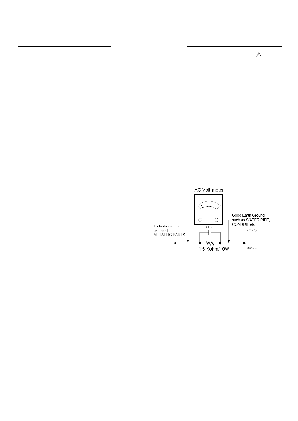
Leakage Current Hot Check (See below Figure)
Plug the AC cord directly into the AC outlet.
Do not use a line Isolation Transformer during this check.
Connect 1.5K/10watt resistor in parallel with a 0.15uF capacitor
between a known good earth ground (Water Pipe, Conduit, etc.)
and the exposed metallic parts.
Measure the AC voltage across the resistor using AC voltmeter with
1000 ohms/volt or more sensitivity.
Reverse plug the AC cord into the AC outlet and repeat AC voltage
measurements for each exposed metallic part. Any voltage
measured must not exceed 0.75 volt RMS which is corresponds to
0.5mA.
In case any measurement is out of the limits specified, there is
possibility of shock hazard and the set must be checked and
repaired before it is returned to the customer.
Leakage Current Hot Check circuit
When 25A is impressed between Earth and 2nd Ground
for 1 second, Resistance must be less than 0.1Ω
*Base on Adjustment standard
Copyright © 2010 LG Electronics. Inc. All right reserved. - 3 - LGE Internal Use Only
Only for training and service purposes
Page 4

CAUTION: Before servicing receivers covered by this service
manual and its supplements and addenda, read and follow the
SAFETY PRECAUTIONS
NOTE:
If unforeseen circumstances create conflict between the
following servicing precautions and any of the safety precautions
on page3 of this publication, always follow the safety precautions.
Remember: Safety First.
General Servicing Precautions
1. Always unplug the receiver AC power cord from the AC power
source before;
a. Removing or reinstalling any component, circuit board
module or any other receiver assembly.
b. Disconnecting or reconnecting any receiver electrical plug or
other electrical connection.
c. Connecting a test substitute in parallel with an electrolytic
capacitor in the receiver.
CAUTION: A wrong part substitution or incorrect polarity
installation of electrolytic capacitors may result in an
explosion hazard.
2. Test high voltage only by measuring it with an appropriate high
voltage meter or other voltage measuring device (DVM,
FETVOM, etc) equipped with a suitable high voltage probe.
Do not test high voltage by "drawing an arc".
3. Do not spray chemicals on or near this receiver or any of its
assemblies.
4. Unless specified otherwise in this service manual, clean
electrical contacts only by applying the following mixture to the
contacts with a pipe cleaner, cotton-tipped stick or comparable
non-abrasive applicator; 10% (by volume) Acetone and 90%
(by volume) isopropyl alcohol (90%-99% strength)
CAUTION: This is a flammable mixture.
Unless specified otherwise in this service manual, lubrication of
contacts in not required.
5. Do not defeat any plug/socket B+ voltage interlocks with which
receivers covered by this service manual might be equipped.
6. Do not apply AC power to this instrument and/or any of its
electrical assemblies unless all solid-state device heat sinks are
correctly installed.
7. Always connect the test receiver ground lead to the receiver
chassis ground before connecting the test receiver positive lead.
Always remove the test receiver ground lead last.
8.
Use with this receiver only the test fixtures specified in this
service manual.
CAUTION: Do not connect the test fixture ground strap to any
heat sink in this receiver.
Electrostatically Sensitive (ES) Devices
Some semiconductor (solid-state) devices can be damaged easily
by static electricity. Such components commonly are called
Electrostatically Sensitive (ES) Devices.
devices are integrated circuits and some field-effect transistors
and semiconductor "chip" components. The following techniques
should be used to help reduce the incidence of component
damage caused by static by static electricity.
1. Immediately before handling any semiconductor component or
semiconductor-equipped assembly, drain off any electrostatic
charge on your body by touching a known earth ground.
Alternatively, obtain and wear a commercially available
discharging wrist strap device, which should be removed to
prevent potential shock reasons prior to applying power to the
on page 3 of this publication.
SERVICING PRECAUTIONS
Examples of typical ES
unit under test.
2. After removing an electrical assembly equipped with ES
devices, place the assembly on a conductive surface such as
aluminum foil, to prevent electrostatic charge buildup or
exposure of the assembly.
3. Use only a grounded-tip soldering iron to solder or unsolder ES
devices.
4. Use only an anti-static type solder removal device. Some solder
removal devices not classified as "anti-static" can generate
electrical charges sufficient to damage ES devices.
5. Do not use freon-propelled chemicals. These can generate
electrical charges sufficient to damage ES devices.
6. Do not remove a replacement ES device from its protective
package until immediately before you are ready to install it.
(Most replacement ES devices are packaged with leads
electrically shorted together by conductive foam, aluminum foil
or comparable conductive material).
7. Immediately before removing the protective material from the
leads of a replacement ES device, touch the protective material
to the chassis or circuit assembly into which the device will be
installed.
CAUTION: Be sure no power is applied to the chassis or
circuit, and observe all other safety precautions.
8. Minimize bodily motions when handling unpackaged
replacement ES devices. (Otherwise harmless motion such as
the brushing together of your clothes fabric or the lifting of
your foot from a carpeted floor can generate static electricity
sufficient to damage an ES device.)
General Soldering Guidelines
1. Use a grounded-tip, low-wattage soldering iron and appropriate
tip size and shape that will maintain tip temperature within the
range or 500。F to 600。F.
2. Use an appropriate gauge of RMA resin-core solder composed
of 60 parts tin/40 parts lead.
3. Keep the soldering iron tip clean and well tinned.
4. Thoroughly clean the surfaces to be soldered. Use a mall wirebristle(0.5 inch, or 1.25cm) brush with a metal handle.
Do not use freon-propelled spray-on cleaners.
5. Use the following unsoldering technique
a. Allow the soldering iron tip to reach normal temperature.
(500。F to 600。F)
b. Heat the component lead until the solder melts.
c. Quickly draw the melted solder with an anti-static, suction-
type solder removal device or with solder braid.
CAUTION: Work quickly to avoid overheating the circuit
board printed foil.
6. Use the following soldering technique.
a. Allow the soldering iron tip to reach a normal temperature
(500。F to 600。F)
b. First, hold the soldering iron tip and solder the strand
against the component lead until the solder melts.
c. Quickly move the soldering iron tip to the junction of the
component lead and the printed circuit foil, and hold it
there only until the solder flows onto and around both the
component lead and the foil.
CAUTION: Work quickly to avoid overheating the circuit
board printed foil.
d. Closely inspect the solder area and remove any excess or
splashed solder with a small wire-bristle brush.
Copyright © 2010 LG Electronics. Inc. All right reserved. - 4 - LGE Internal Use Only
Only for training and service purposes
Page 5

IC Remove/Replacement
Some chassis circuit boards have slotted holes (oblong) through
which the IC leads are inserted and then bent flat against the
circuit foil. When holes are the slotted type, the following
technique should be used to remove and replace the IC. When
working with boards using the familiar round hole, use the
standard technique as outlined in paragraphs 5 and 6 above.
Removal
1. Desolder and straighten each IC lead in one operation by gently
prying up on the lead with the soldering iron tip as the solder
melts.
2. Draw away the melted solder with an anti-static suction-type
solder removal device (or with solder braid) before removing
the IC.
Replacement
1. Carefully insert the replacement IC in the circuit board.
2. Carefully bend each IC lead against the circuit foil pad and
solder it.
3. Clean the soldered areas with a small wire-bristle brush.
(It is not necessary to reapply acrylic coating to the areas).
"Small-Signal" Discrete Transistor
Removal/Replacement
1. Remove the defective transistor by clipping its leads as close as
possible to the component body.
2. Bend into a "U" shape the end of each of three leads remaining
on the circuit board.
3. Bend into a "U" shape the replacement transistor leads.
4. Connect the replacement transistor leads to the corresponding
leads extending from the circuit board and crimp the "U" with
long nose pliers to insure metal to metal contact then solder
each connection.
Power Output, Transistor Device
Removal/Replacement
1. Heat and remove all solder from around the transistor leads.
2. Remove the heat sink mounting screw (if so equipped).
3. Carefully remove the transistor from the heat sink of the circuit
board.
4. Insert new transistor in the circuit board.
5. Solder each transistor lead, and clip off excess lead.
6. Replace heat sink.
Diode Removal/Replacement
1. Remove defective diode by clipping its leads as close as possible
to diode body.
2. Bend the two remaining leads perpendicular y to the circuit
board.
3. Observing diode polarity, wrap each lead of the new diode
around the corresponding lead on the circuit board.
4. Securely crimp each connection and solder it.
5. Inspect (on the circuit board copper side) the solder joints of
the two "original" leads. If they are not shiny, reheat them and if
necessary, apply additional solder.
Fuse and Conventional Resistor
Removal/Replacement
1. Clip each fuse or resistor lead at top of the circuit board hollow
stake.
2. Securely crimp the leads of replacement component around
notch at stake top.
3. Solder the connections.
CAUTION: Maintain original spacing between the replaced
component and adjacent components and the circuit board to
prevent excessive component temperatures.
Circuit Board Foil Repair
Excessive heat applied to the copper foil of any printed circuit
board will weaken the adhesive that bonds the foil to the circuit
board causing the foil to separate from or "lift-off" the board. The
following guidelines and procedures should be followed whenever
this condition is encountered.
At IC Connections
To repair a defective copper pattern at IC connections use the
following procedure to install a jumper wire on the copper pattern
side of the circuit board. (Use this technique only on IC
connections).
1. Carefully remove the damaged copper pattern with a sharp
knife. (Remove only as much copper as absolutely necessary).
2. carefully scratch away the solder resist and acrylic coating (if
used) from the end of the remaining copper pattern.
3. Bend a small "U" in one end of a small gauge jumper wire and
carefully crimp it around the IC pin. Solder the IC connection.
4. Route the jumper wire along the path of the out-away copper
pattern and let it overlap the previously scraped end of the
good copper pattern. Solder the overlapped area and clip off
any excess jumper wire.
At Other Connections
Use the following technique to repair the defective copper pattern
at connections other than IC Pins. This technique involves the
installation of a jumper wire on the component side of the circuit
board.
1. Remove the defective copper pattern with a sharp knife.
Remove at least 1/4 inch of copper, to ensure that a hazardous
condition will not exist if the jumper wire opens.
2. Trace along the copper pattern from both sides of the pattern
break and locate the nearest component that is directly
connected to the affected copper pattern.
3. Connect insulated 20-gauge jumper wire from the lead of the
nearest component on one side of the pattern break to the lead
of the nearest component on the other side.
Carefully crimp and solder the connections.
CAUTION: Be sure the insulated jumper wire is dressed so the
it does not touch components or sharp edges.
Copyright © 2010 LG Electronics. Inc. All right reserved. - 5 - LGE Internal Use Only
Only for training and service purposes
Page 6
SPECIFICATION
NOTE : Specifications and others are subject to change without notice for improvement.
1. Application Range. 3. Test method
This spec sheet is applied to the 32"/37”/42"/47” LED TV used LE?? 1) Performance : LGE TV test method followed.
chassis. 2) Demanded other specification
- Safety : CE, IEC specification
2. Specification -
Each part is tested as below without special appointment.
1) Temperature : 25±5°C(77±9°F), CST : 40±5°C
2) Relative Humidity : 65±10%
3) Power Voltage : Standard input voltage (100~240V@ 50/60Hz)
• Standard Voltage of each products is marked by models
4) Specification and performance of each parts are followed
each drawing and specification by part number in
accordance with BOM .
5) The receiver must be operated for about 5 minutes prior to
the adjustment.
EMC : CE, IEC
4. Module General Specification
No Item Specification Remark
1 Display Screen Device 32”/37”/42”/47” wide Color Display Module LCD with an integral LED backlight
2 Aspect Ratio 16:9
3 LCD Module 32” / 37” / 42”/ 47” Gate in Panel LGD
4 Storage Environment
5 Input Voltage AC100 ~ 240V, 50/60Hz
6 Power Consumption
7 Module Size
Pixel Pitch
8
Back Light
9
Temp. : -20 ~ 60 deg
Humidity : 10 ~ 90 %
Power ON
32” 73.2W LGD
37” 79.7W LGD
42” 98.0W LGD
47” 110.5W LGD
32” 741.1(H) x 435.8(V) x 10.8(D) LGD
37” 862.4(H) x 504.0(V) x 10.8(D) LGD
42” 973.2(H) x 566.2(V) x 10.8(D) LGD
47” 1083.6(H) x 628.80(V) x 10.8(D) LGD
32” 0.36375(H) x 0.36375(V) LGD
32” 0.42675(H) x 0.42675(V) LGD
42” 0.48450(H) x 0.48450(V) LGD
0.54150(H) x 0.54150(V) LGD
32” LED LGD
37” LED LGD
42” LED LGD
47” LED
10 Display Colors 1.06 Billion Color, 16.7M(others)
11 Coating 3H, AG
Copyright © 2010 LG Electronics. Inc. All right reserved. - 6 - LGE Internal Use Only
Only for training and service purposes
Page 7
g
g
5. Module optical specification
* 32” LED Module (LGD FHD 100Hz)
for more details, refer to the module spec.
No. Item Specification Min. Typ. Max. Remark
Ri
1. Viewing Angle(CR>10)
2. Luminance
3. Contrast Ratio CR 900 1300
4. CIE Color Coordinates
1) Standard Test Condition (The unit has been ‘ON’)
2) Stable for approximately 30 minutes in a dark environment at 25±2℃
3) The values specified are at approximate distance 50Cm from the LCD surface
4) Ta= 25±2°C, VDD, H_VDD, VGH, VGL=typ, fV=120Hz, Clk+297MHz, If = 165mA (Typ)
ht/Left (Up/Down)
2
Luminance (cd/m
Variation - 1.3 MAX / MIN
RED
Green
Blue
White
) 360 450
Rx
Ry 0.332
Gx 0.308
Gy 0.597
Bx 0.149
By 0.059
Wx 0.279
Wy 0.292
178 Degree
0.651
32LE5400-ZA/NL
32LE5410-ZA/DE
Typ
-0.03
Typ
+0.03
32LE5700-ZC/CH
32LE5700/EU
32LE5710-ZD/GB
32LE5750-ZC/IT
* 37” LED Module (LGD FHD 100Hz)
for more details, refer to the module spec.
No. Item Specification Min. Typ. Max. Remark
Ri
1. Viewing Angle(CR>10)
2. Luminance
3. Contrast Ratio CR 1000 1400
4. CIE Color Coordinates
1) Standard Test Condition (The unit has been ‘ON’)
2) Stable for approximately 30 minutes in a dark environment at 25±2℃
3) The values specified are at approximate distance 50Cm from the LCD surface
4) Ta= 25±2°C, VDD, H_VDD, VGH, VGL=typ, fV=120Hz, Clk+297MHz, If = 165mA (Typ)
ht/Left (Up/Down)
2
Luminance (cd/m
Variation - 1.3 MAX / MIN
RED
Green
Blue
White
) 360 450
Rx
Ry 0.332
Gx 0.306
Gy 0.604
Bx 0.150
By 0.058
Wx 0.279
Wy 0.292
178 Degree
0.647
Typ
-0.03
Typ
+0.03
37LE5400-ZA/NL
37LE5410-ZA/DE
37LE5710-ZD/GB
Copyright © 2010 LG Electronics. Inc. All right reserved. - 7 - LGE Internal Use Only
Only for training and service purposes
Page 8
g
g
* 42” LED Module (LGD FHD 100Hz)
for more details, refer to the module spec.
No. Item Specification Min. Typ. Max. Remark
Ri
1. Viewing Angle(CR>10)
2. Luminance
3. Contrast Ratio CR 1000 1400
4. CIE Color Coordinates
1) Standard Test Condition (The unit has been ‘ON’)
2) Stable for approximately 30 minutes in a dark environment at 25±2℃
3) The values specified are at approximate distance 50Cm from the LCD surface
4) Ta= 25±2°C, VDD, H_VDD, VGH, VGL=typ, fV=120Hz, Clk+297MHz, If = 165mA (Typ)
ht/Left (Up/Down)
Luminance (cd/m
Variation - 1.3 MAX / MIN
RED
Green
Blue
White
2
) 360 450
Rx
Ry 0.332
Gx 0.309
Gy 0.601
Bx 0.149
By 0.059
Wx 0.279
Wy 0.292
178 Degree
0.647
42LE5400-ZA/NL
42LE5410-ZA/DE
Typ
-0.03
Typ
+0.03
42LE5700-ZC/CH
42LE5700/EU
42LE5710-ZD/GB
42LE5750-ZC/IT
* 47” LED Module (LGD FHD 100Hz)
for more details, refer to the module spec.
No. Item Specification Min. Typ. Max. Remark
Ri
1. Viewing Angle(CR>10)
2. Luminance
3. Contrast Ratio CR 1000 1400
4. CIE Color Coordinates
1) Standard Test Condition (The unit has been ‘ON’)
2) Stable for approximately 30 minutes in a dark environment at 25±2℃
3) The values specified are at approximate distance 50Cm from the LCD surface
4) Ta= 25±2°C, VDD, H_VDD, VGH, VGL=typ, fV=120Hz, Clk+297MHz, If = 165mA (Typ)
ht/Left (Up/Down)
Luminance (cd/m
Variation - 1.3 MAX / MIN
RED
Green
Blue
White
2
) 360 450
Rx
Ry 0.332
Gx 0.307
Gy 0.595
Bx 0.149
By 0.059
Wx 0.279
Wy 0.292
178 Degree
0.649
42LE5400-ZA/NL
42LE5410-ZA/DE
Typ
-0.03
Typ
+0.03
42LE5700-ZC/CH
42LE5700/EU
42LE5710-ZD/GB
42LE5750-ZC/IT
Copyright © 2010 LG Electronics. Inc. All right reserved. - 8 - LGE Internal Use Only
Only for training and service purposes
Page 9

6. Component Video Input (Y, Cb/Pb, Cr/Pr)
No Resolution H-freq(kHz) V-freq.(kHz) Pixel clock(MHz) Proposed Remark
1 720*480 15.73 59.94 13.500 SDTV, DVD 480I(525I)
2 720*480 15.75 60.00 13.514 SDTV, DVD 480I(525I)
3 720*576 15.625 50.00 13.500
4 720*480 31.47 59.94 27.000 SDTV 480P
5 720*480 31.50 60.00 27.027 SDTV 480P
6 720*576 31.25 50.00 27.000 SDTV 576P 50Hz
7 1280*720 44.96 59.94 74.176 HDTV 720P
8 1280*720 45.00 60.00 74.250 HDTV 720P
9 1280*720 37.50 50.00 74.25 HDTV 720P 50Hz
10 1920*1080 33.72 59.94 74.176 HDTV 1080I
SDTV, DVD 576I(625I)
50Hz
11 1920*1080 33.75 60.00 74.250 HDTV 1080I
12 1920*1080 28.125 50.00 74.250 HDTV 1080I 50Hz,
13 1920×1080 56.25 50 148.50 HDTV 1080P
14 1920×1080 67.5 60 148.50 HDTV 1080P
7. RGB PC
No Resolution H-freq(kHz) V-freq.(Hz) Pixel clock(MHz) Proposed Remark
1. 720*400 31.468 70.08 28.32 For only DOS mode
2. 640*480 31.469 59.94 25.17 VESA
3. 800*600 37.879 60.31 40.00 VESA
4. 1024*768 48.363 60.00 65.00 VESA(XGA)
Input 848*480 60Hz, 852*
-> 640*480 60Hz Display
5. 1280*768 47.78 59.87 80.125 WXGA
6 1360*768 47.78 59.80 84.75 WXGA FHD model
7 1366*768 47.72 59.60 84.75 WXGA WXGA model
8 1280*1024 63.595 60.02 108.875 SXGA FHD model
9 1280*720 45 60 74.25 720p DTV Standard
10. 1920*1080 66.587 59.934 138.5 WUXGA FHD model
Copyright © 2010 LG Electronics. Inc. All right reserved. - 9 - LGE Internal Use Only
Only for training and service purposes
Page 10

8. HDMI Input
8-1. DTV Mode
No Resolution H-freq(kHz) V-freq.(kHz) Pixel clock(MHz) Proposed Remark
1 640*480 31.649 59.94 25.175 SDTV 480p 60Hz
2 640*480 31.469 60 25.20 SDTV 480p 60Hz
3 720*480 31.47 59.94 27.00 SDTV 480p 60Hz
4 720*480 31.50 60 27.027 SDTV 480p 60Hz
5 720*576 31.25 50.00 27.00 SDTV 576p 50Hz
6 1280*720 37.50 50.00 74.176 HDTV 720p 50Hz
7 1280*720 44.96 59.94 74.176 HDTV 720p 60Hz
8 1280*720 45.00 60 74.250 HDTV 720p 60Hz
9 1920*1080 28.125 50.00 74.250 HDTV 1080i 50Hz
10 1920*1080 33.72 59.94 74.176 HDTV 1080i 60Hz
11 1920*1080 33.75 60 74.250 HDTV 1080i 60Hz
12 1920*1080 27.00 24.00 74.25 HDTV 1080p 24Hz
13 1920*1080 33.750 30 74.25 HDTV 1080p 30Hz
14 1920*1080 56.25 50.00 148.50 HDTV 1080p 50Hz
15 1920*1080 67.433 59.94 148.352 HDTV 1080p 60Hz
16 1920*1080 67.50 60 148.50 HDTV 1080p 60Hz
8-2. PC Mode
No Resolution H-freq(kHz) V-freq.(Hz) Pixel clock(MHz) Proposed Remark
1. 720*400 31.468 70.08 28.32 HDCP
2. 640*480 31.469 59.94 25.17 VESA HDCP
3. 800*600 37.879 60.31 40.00 VESA HDCP
4. 1024*768 48.363 60.00 65.00 VESA(XGA) HDCP
5. 1280*768 47.78 59.87 80.125 VESA(WXGA) HDCP
6 1360*768 47.72 59.80 84.625 VESA(WXGA) HDCP
7 1280*1024 63.98 60.02 108. SXGA HDCP
8 1400*1050 65.317 59.979 121.75 SXGA HDCP
9. 1920*1080 66.587 59.934 138.5 WUXGA HDCP
Copyright © 2010 LG Electronics. Inc. All right reserved. - 10 - LGE Internal Use Only
Only for training and service purposes
Page 11
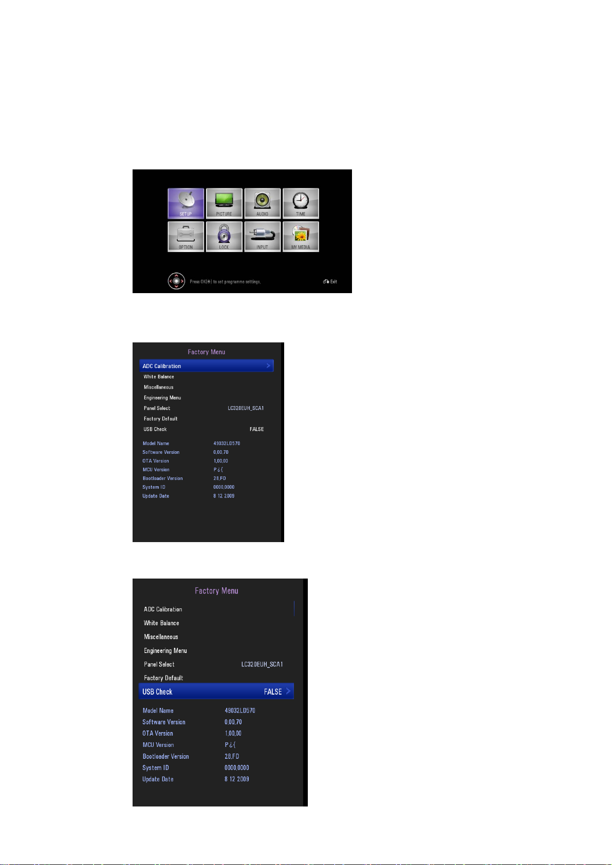
1. Software version up.
1.1. USB DOWNLOAD
1) Press “Menu” Key and select “OK” key after focusing “SETUP” item
2) Press Numeric Keys like following sequences : 1 – 2 – 4 – 7 – 5
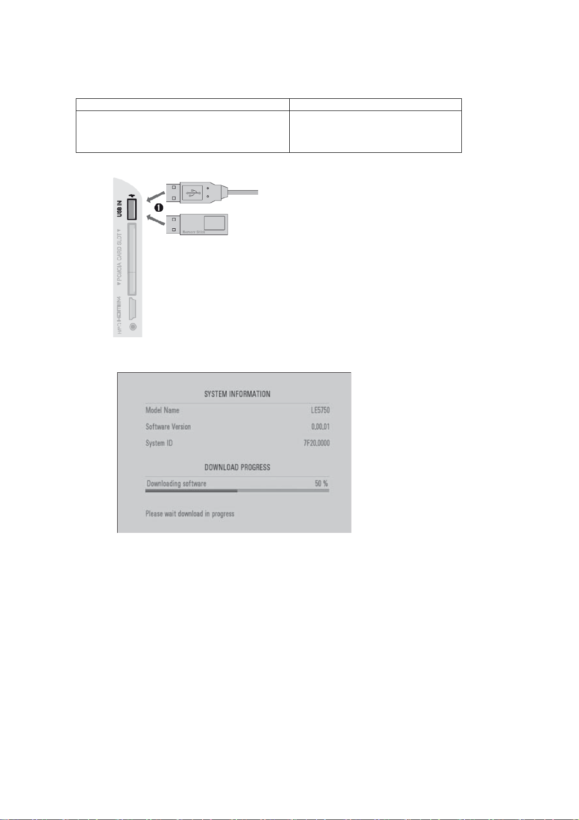
3) Factory menu will be displayed
ADJUSTMENT INSTRUCTION
4) press “OK” key after focusing “USB Check” item, then “USB Check” item value will be
changed to “TRUE”
Copyright © 2010 LG Electronics. Inc. All right reserved. - 11 - LGE Internal Use Only
Only for training and service purposes
Page 12
5) Copy SW upgrade image “xxxxxx.hdf” to an USB memory stick.
File name Ex.)
Model Name Upgrade image file name
32/42LE5700
32/37/42/47LE5400
32/42LE5750
LE5700.hdf
LE5400.hdf
LE5750.hdf
6) Connects USB memory stick to the side jack(USB IN) of TV
7) Turn Off and On TV with using AC-Power.
8) After Turning on TV, Software upgrade will be done automatically.
9) After upgrading SW, turn off TV and wait 20 second
10) Turn on TV, Check SW version in Diagnostics of SETUP
1.2. Function Check
1) Check display and sound.
2) Check Input and Signal items.(cf. work instructions)
a) TV & DTV
b) AV(SCART, CVBS)
c) COMPONENT(480i)
d) RGB(PC : 1024 x 768 @60Hz)
e) HDMI
f) PC Audio In
3) Display and Sound Check is executed by Remote control.
Copyright © 2010 LG Electronics. Inc. All right reserved. - 12 - LGE Internal Use Only
Only for training and service purposes
Page 13
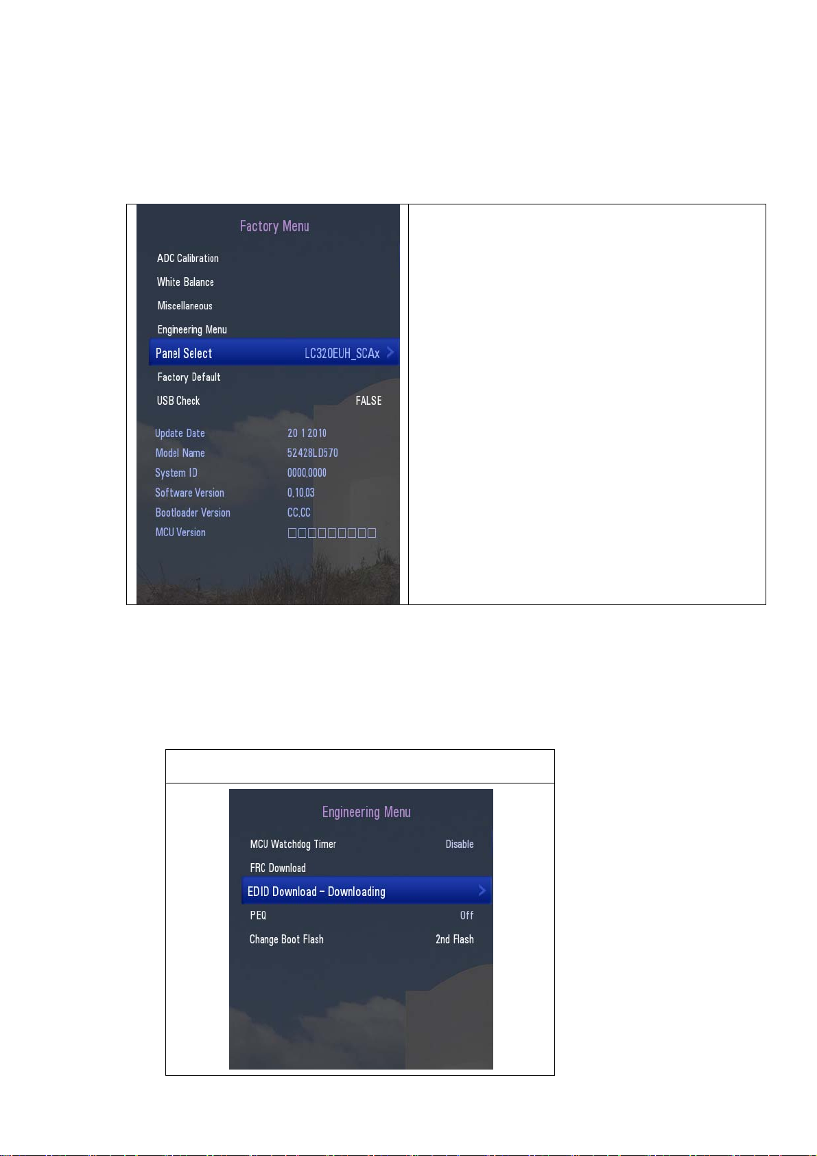
2. EDID DOWNLOAD
2-1. Panel Setting
a) You should change the panel size by going to the Factory Mode, press “Menu”, “1”, “2”, “4”, 7”
and “5” keys on a remote.
b) You have to select 32” or 37”, 42”, 47” panel in Factory mode.
32LE5400-ZA : Panel Select “LC320EUH_SCAx”
32LE5700-ZC : Panel Select “LC320EUH_SCAx”
32LE5750-ZC : Panel Select “LC320EUH_SCAx”
37LE5400-ZA : Panel Select “LC370EUH_SCAx”
42LE5400-ZA : Panel Select “LC420EUH_SCAx”
42LE5700-ZC : Panel Select “LC420EUH_SCAx”
42LE5750-ZC : Panel Select “LC420EUH_SCAx”
47LE5400-ZA : Panel Select “LC470EUH_SCAx”
2-2. EDID Setting
a) You should change the panel size by going to the Factory Mode, press “Menu”, “1”, “2”, “4”, 7”
and “5” keys on a remote.
b) You have to select “Engineering Menu” in Factory mode.
c) Enter “ EDID Download” by pushing “OK” key.
Factory mode Engineering menu EDID Download select
Copyright © 2010 LG Electronics. Inc. All right reserved. - 13 - LGE Internal Use Only
Only for training and service purposes
Page 14
2-3. PC EDID Table
00 FF FF FF FF FF FF 00 1E 6D ⓐ ⓑ
01 ⓒ 03 80 46 28 78 2A C0 0B A3 57 49 9C 25
11 47 4A A1 08 00 31 40 45 40 61 40 D1 C0 81 80
01 01 01 01 01 01 26 36 80 A0 70 38 1F 40 30 20
25 00 BA 88 21 00 00 1A 16 21 50 A0 51 00 1E 30
48 88 35 00 BA 88 21 00 00 1E 00 00 00 FD 00 39
3E 1E 53 10 00 0A 20 20 20 20 20 20 ⓓ
ⓓ 01 ⓔ
2-4. HDMI EDID Table
00 FF FF FF FF FF FF 00 1E 6D ⓐ ⓑ
01 ⓒ 03 80 46 28 78 2A C0 0B A3 57 49 9C 25
11 47 4A A1 08 00 31 40 45 40 61 40 D1 C0 81 80
01 01 01 01 01 01 02 3A 80 18 71 38 2D 40 58 2C
45 00 BA 88 21 00 00 1E 16 21 50 A0 51 00 1E 30
48 88 35 00 BA 88 21 00 00 1E 00 00 00 FD 00 3A
3E 1E 53 10 00 0A 20 20 20 20 20 20 ⓓ
02 03 23 F1 4E 90 1F 20 22 11 05 14 04 13 12 03
02 15 01 23 09 17 07 83 01 00 00 ⓕ
ⓕ 2D 01 1D 00 72 51 D0 1E 20 6E 28 55 00 BA
88 21 00 00 1E 8C 0A D0 8A 20 E0 2D 10 10 3E 96
00 BA 88 21 00 00 18 02 3A 80 18 71 38 2D 40 58
2C 45 00 BA 88 21 00 00 1E 01 1D 80 18 71 1C 16
20 58 2C 25 00 BA 88 21 00 00 9E 00 00 00 00 00
00 00 00 00 00 00 00 00 00 00 00 00 00 00 00 43
☞ Detail EDID Options are below
ⓐ Product ID
Model Name HEX EDID table DDC Function
FHD Model 0001 01 00 Analog / Digital
ⓑ Serial No: Controlled on production line.
ⓒ Month, Year: Controlled on production line:
ex) Monthly : ‘03’ -> ‘03’
Year : ‘2010’ -> ‘13’
ⓓ Model Name(Hex) :
Model MODEL NAME (HEX)
ⓓ 01 ⓔ
All 00 00 00 FC 00 4C 47 20 54 56 0A 20 20 20 20 20 20 20
ⓔ Checksum : Changeable by total EDID data.
ⓕ Vendor Specific(HDMI)
INPUT MODEL NAME (HEX)
HDMI 1 67030C001000B82D
HDMI 2 67030C002000B82D
HDMI 3 67030C003000B82D
HDMI 4 67030C004000B82D
Copyright © 2010 LG Electronics. Inc. All right reserved. - 14 - LGE Internal Use Only
Only for training and service purposes
Page 15
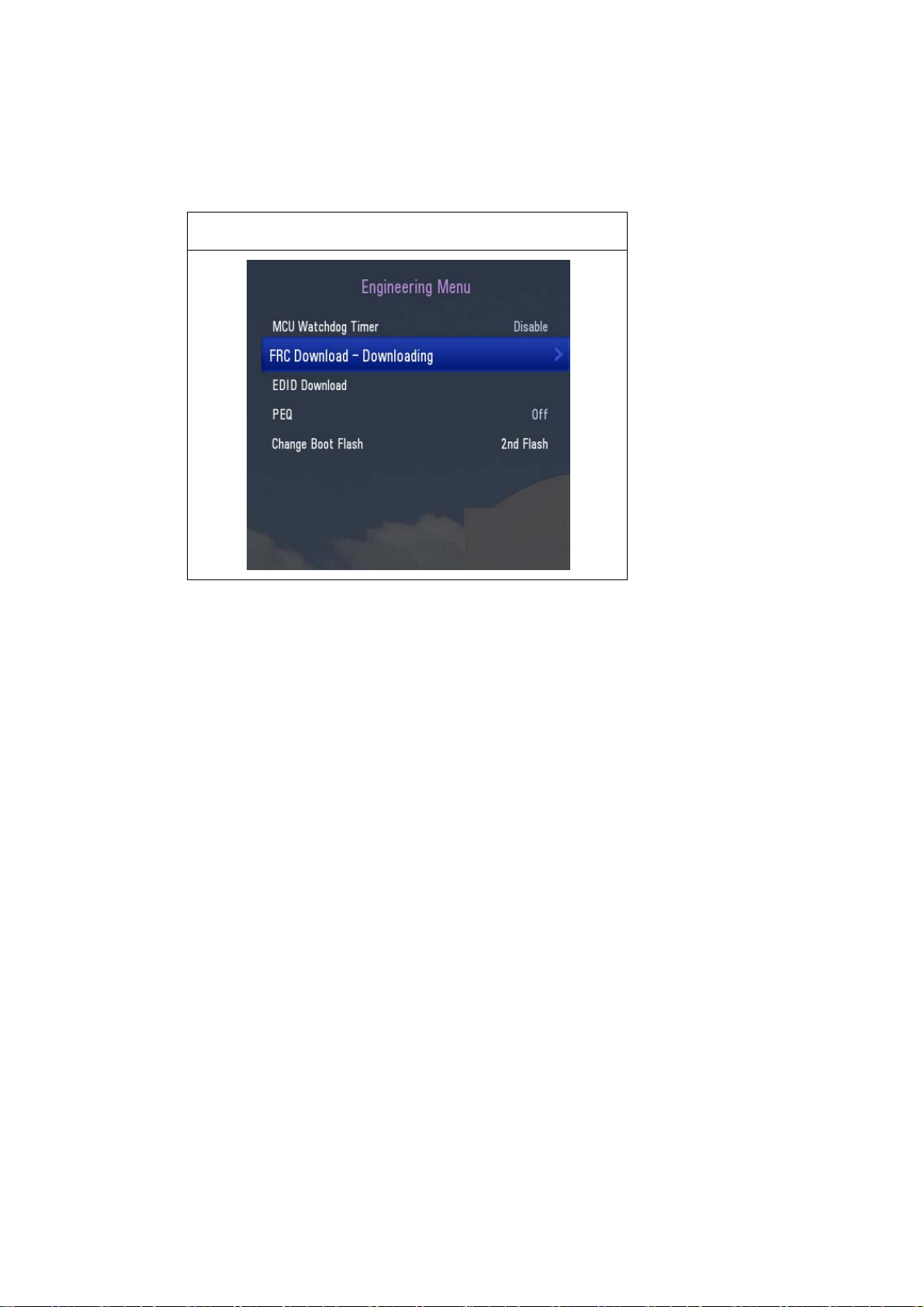
3. FRC DOWNLOAD
a) You should change the panel size by going to the Factory Mode, press “Menu”, “1”, “2”, “4”, 7”
and “5” keys on a remote.
b) You have to select “Engineering Menu” in Factory mode.
c) Enter “ FRC Download” by pushing “OK” key.
Factory mode Engineering menu DRC Download select
Copyright © 2010 LG Electronics. Inc. All right reserved. - 15 - LGE Internal Use Only
Only for training and service purposes
Page 16
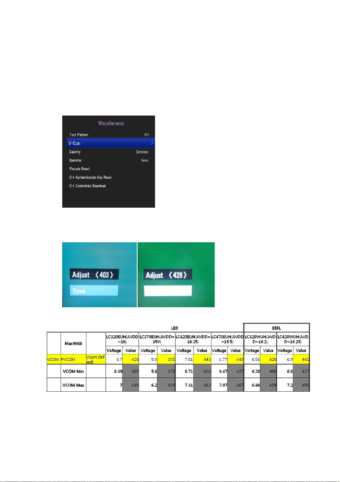
4. V-COM Adjust(Only LGD Module)
a) Why need Vcom adjustment?
■ The Vcom (Common Voltage) is a Reference Voltage of Liquid Crystal Driving.
Liquid Crystal need for Polarity Change with every frame.
b) Adjust sequence
■ You should change the panel size by going to the Factory Mode, press “Menu”, “1”, “2”, “4”, 7”
and “5” keys on a remote.
■ You have to select “Miscellaneous” in Factory mode.
■ Enter “ V-Com” by pushing “OK” key.
■ As pushing the right or the left key on the remote control, and find the V-COM value which is no
or minimized the Flicker.
(If there is no flicker at default value, Press the exit key and finish the VCOM adjustment.)
[LED/LCD Panel VCOM SPEC .]
■ Push the “OK” key to store value. Then the message “Saving OK” is pop.
Copyright © 2010 LG Electronics. Inc. All right reserved.
Only for training and service purposes
- 16 -
LGE Internal Use Only
Page 17
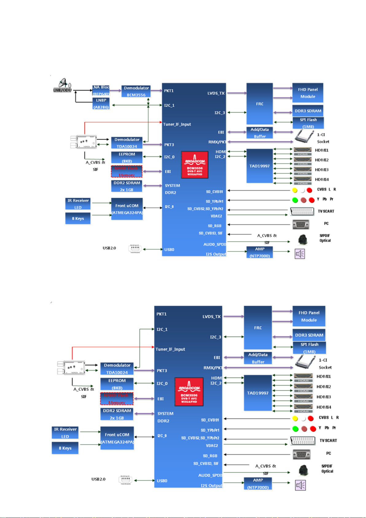
BLOCK DIAGRAM
1. 32/42LE5700 Block diagram(T+C+S)
2. 32/37/42/47LE5400 Block diagram (T+C)
Copyright © 2010 LG Electronics. Inc. All right reserved. - 17 - LGE Internal Use Only
Only for training and service purposes
Page 18
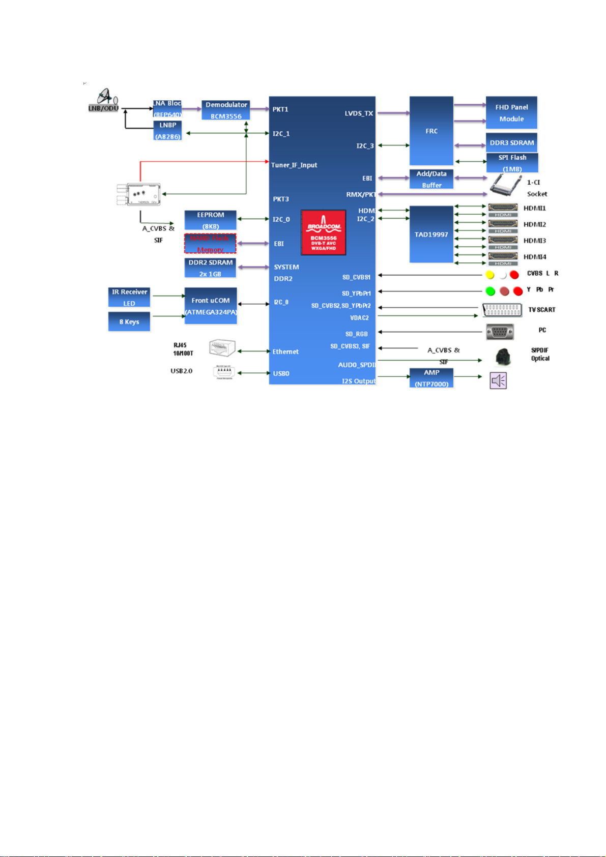
3. 32/42LE5750 Block diagram (T+S)
Copyright © 2010 LG Electronics. Inc. All right reserved. - 18 - LGE Internal Use Only
Only for training and service purposes
Page 19

MEMO
Copyright © 2010 LG Electronics. Inc. All right reserved. - 19 - LGE Internal Use Only
Only for training and service purposes
Page 20
- 20 -
LGE Internal Use OnlyCopyright LG Electronics. Inc. All right reserved.
Only for training and service purposes
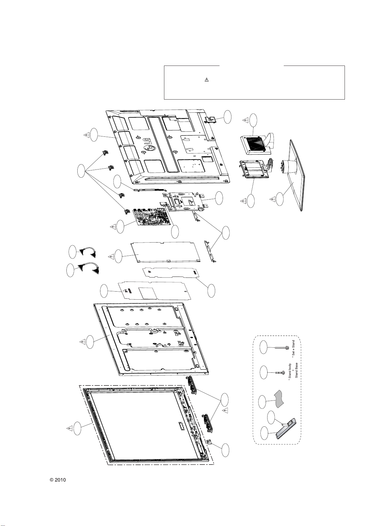
EXPLODED VIEW
300
200
500
120
A2
A5
A9
A10
A21
840
530
800
LV1
LV2
810
830
540
880
820
521
900
920
710
910
400
Many electrical and mechanical parts in this chassis have special safety-related characteristics. These
parts are identified by in the Schematic Diagram and EXPLODED VIEW.
It is essential that these special safety parts should be replaced with the same components as
recommended in this manual to prevent X-RADIATION, Shock, Fire, or other Hazards.
Do not modify the original design without permission of manufacturer.
IMPORTANT SAFETY NOTICE
Page 21

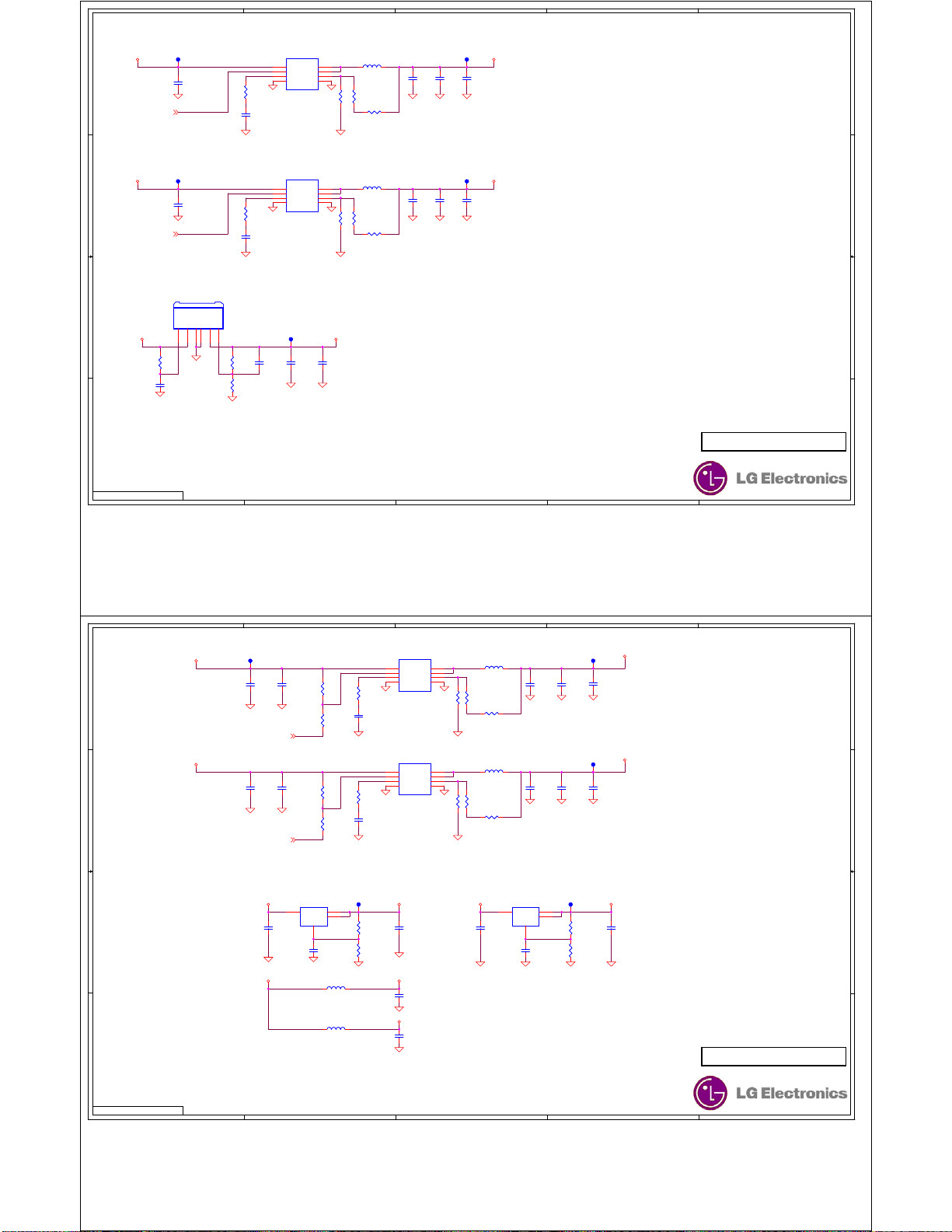
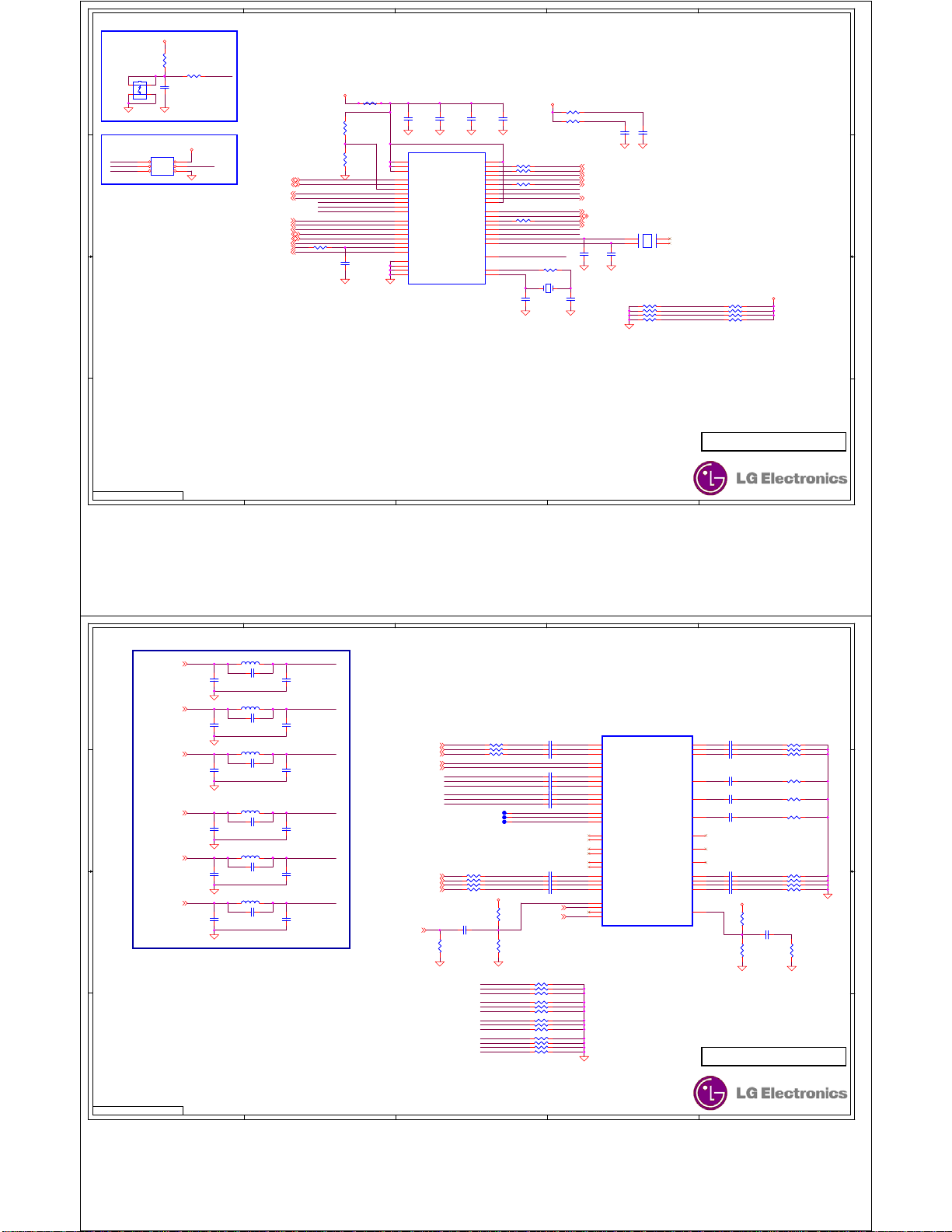
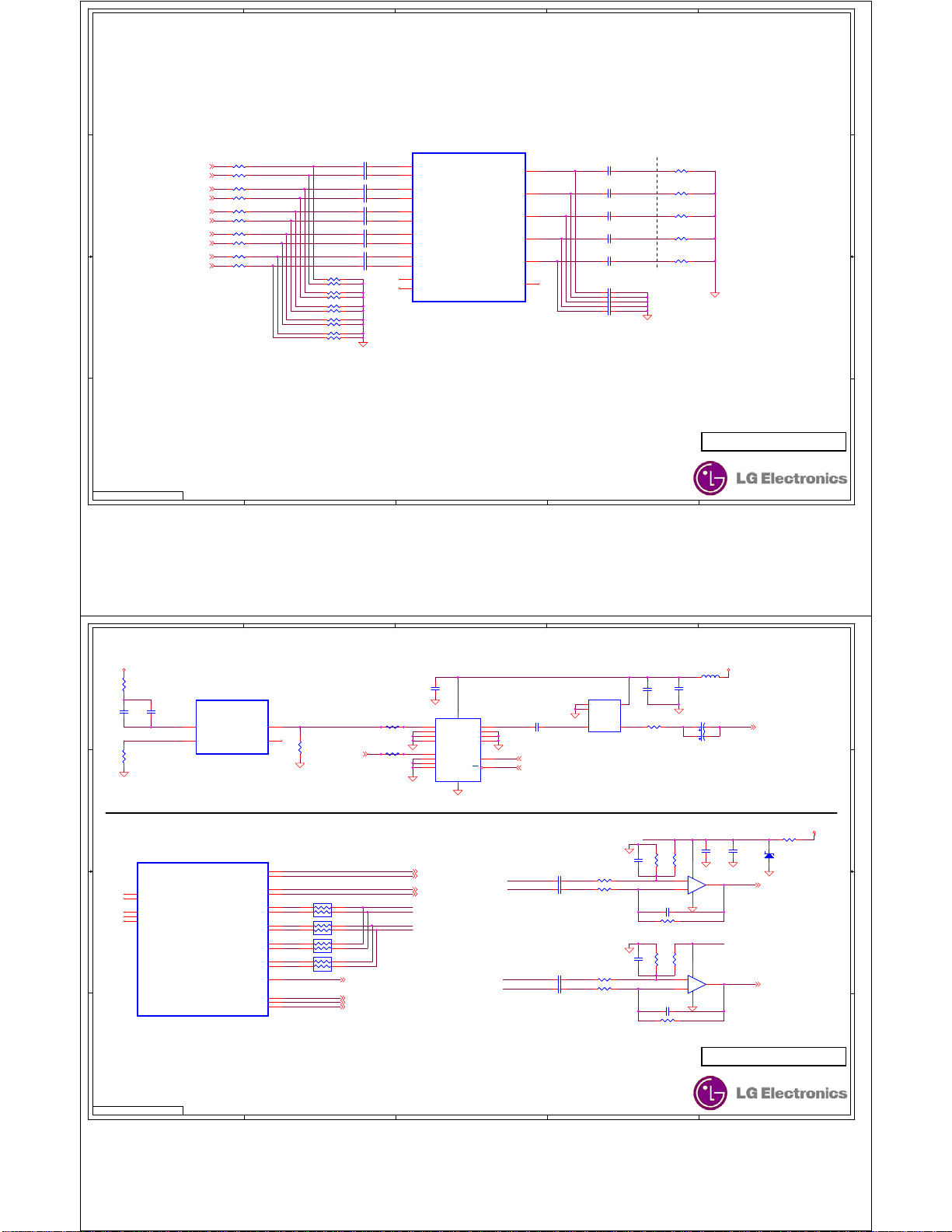
SCHEMATIC DIAGRAMME
32/42LE5700-ZC
Copyright © 2010 LG Electronics. Inc. All right reserved. - 21 - LGE Internal Use Only
Only for training and service purposes
Page 22

5
Copyright © 2010 LG Electronics. Inc. All rights reserved.
Only for training and service purposes
LGE Internal Use Only
JP1
JP1
SMAW200-H24S(BK)
SMAW200-H24S(BK)
D D
JP2
JP2
12505WR-15A
12505WR-15A
C C
1.25mm
1.25mm
B B
SMPS_ON
232426
22
21
20
19
18
17
16
15
14
2mm
2mm
13
12
11
10
9
8
BL_EN_O
7
6
ANA_DIM
5
4
3
2
25
1
1
2
3
4
5
6
17
7
16
8
9
10
11
12
13
14
15
1
TP1 PCB_TP10TP1 PCB_TP10
1
TP2 PCB_TP10TP2 PCB_TP10
1
TP3 PCB_TP10TP3 PCB_TP10
1
TP4 PCB_TP10TP4 PCB_TP10
1
TP5 PCB_TP10TP5 PCB_TP10
1
TP6 PCB_TP10TP6 PCB_TP10
1
TP7 PCB_TP10TP7 PCB_TP10
1
TP8 PCB_TP10TP8 PCB_TP10
1
TP9 PCB_TP10TP9 PCB_TP10
1
TP10 PCB_TP10TP10 PCB_TP10
1
TP11 PCB_TP10TP11 PCB_TP10
1
TP12 PCB_TP10TP12 PCB_TP10
1
TP13 PCB_TP10TP13 PCB_TP10
C10
C10
OPEN-104p/16V/1005
OPEN-104p/16V/1005
R5 102/1005R5 102/1005
R8 103/1005R8 103/1005
C16
C16
104p/16V/1005
104p/16V/1005
U1
FDS6675BZU1FDS6675BZ
3V4_STB
R23
R23
103/1005
103/1005
R11 100/1005R11 100/1005
R12 100/1005R12 100/1005
R28 152/1005R28 152/1005
R18 152/1005R18 152/1005
R17 OPEN-101/1005R17 OPEN-101/1005
R31 101/1005R31 101/1005
R39 000/1005R39 000/1005
8
D15D26D37D4
S11S22S33G
4
TP15
TP15
PCB_TP10
PCB_TP10
1
L2
L2
OPEN-CIC41P600AE
OPEN-CIC41P600AE
PWM1_DIM [11]
PANEL_ER [11]
LED_B
C17
C17
225p/16V
225p/16V
KEY_ADC1 [6]
KEY_ADC2 [6]
LED_B [6]
IR_IN [6]
PWM_BUZZ [6]
LED_R [6]
CDS_OUT [6]
3V4
4
C4
C4
OPEN-100uF/16V/MVK/S
OPEN-100uF/16V/MVK/S
3V3_BCM3556
TP14
TP14
PCB_TP10
PCB_TP10
1
R34
R34
OPEN-121/3216
OPEN-121/3216
3V4_STB
3
20V_SMPS
C2
104p/50VC2104p/50V
3V4_STB
C3
104p/50VC3104p/50V
12V_SMPS
C6
104p/50VC6104p/50V
3V4_STB
R9
R10
R10
472/1005R9472/1005
472/1005
472/1005
ATM_SCL [6]
ATM_SDA_IN [6]
1
R14
R14
ATM_SDA_OUT [6]
103/1005
103/1005
Q3
2 3
MMBT4401Q3MMBT4401
5V
12V_SMPS
D2
ZMMC6V2D2ZMMC6V2
1 2
R43
R43
472/1005
472/1005
R42
R42
472/1005
472/1005
DC_EN [2,3,5]
2
R4 103/1005R4 103/1005
STBY_EN[6]
R13 102/1005R13 102/1005
A_DIM[11]
3V3_BCM3556 3V3_BCM3556
R20
R20
103/1005
103/1005
R22 103/1005R22 103/1005
BLT_EN[11]
12V_SMPS
D1
ZMMC6V2D1ZMMC6V2
1 2
R33
R33
103/1005
103/1005
C9
105p/16V/1005C9105p/16V/1005
U2
KIA7042AFU2KIA7042AF
VCC1GND2OUT3GND
3V4_STB
1
1
4
Q1
23
MMBT4403Q1MMBT4403
R21
R21
102/1005
102/1005
R40 101/1005R40 101/1005
Q4
MMBT4401Q4MMBT4401
2 3
R35
R35
103/1005
103/1005
R36
R36
203/1005
203/1005
1
SMPS_ON
ANA_DIM
BL_EN_O
AC_DETECT [6,36,38]
1
A A
All location are from 01 to 50
12V_SMPS
D D
C C
3V3_BCM3556
B B
A A
All location are from 50 to 100
TP10
TP10
TP50
TP50
TP10
TP10
TP52
TP52
TP10
TP10
TP54
TP54
L57
L57
CIS41P600AE
CIS41P600AE
INSTANT_BOOT[6]
L61
L61
OPEN-CIC10P300NC
OPEN-CIC10P300NC
5
5
1
1
1
R67 475/1005R67 475/1005
R72 OPEN-330/1005R72 OPEN-330/1005
+1V8
A2V5_BCM3556
C87
C87
104p/16V/1005
104p/16V/1005
5
C73
C73
102p/50V/1005
102p/50V/1005
Q5
2 3
MMBT4401Q5MMBT4401
C51
C51
106p/16V/2012
106p/16V/2012
DC_EN[1,3,5]
C60
C60
106p/16V/2012
106p/16V/2012
DC_EN[1,3,5]
2
5
6
7
C52
C52
106p/16V/2012
106p/16V/2012
C61
C61
106p/16V/2012
106p/16V/2012
R62
R62
OPEN-104/F/1005
OPEN-104/F/1005
R63
R63
103/1005
103/1005
R64
R64
3093/F/1005
3093/F/1005
C79
C79
122p/50V/1005
122p/50V/1005
U54
U54
EUP7996
EUP7996
NSD
VDDQ
AVIN
PVIN
R25 103/1005R25 103/1005
VSENSE
9
SMPS_ON
GND_D DGND
4
4
U50
U50
AOZ1073AIL/SO-8L
AOZ1073AIL/SO-8L
2
8
VIN
LX
6
LX7EN
5
FB
COMP
3
PGND
AGND
R51
R51
153/1005
153/1005
C58
C58
222p/50V/1005
222p/50V/1005
U51
U51
AOZ1073AIL/SO-8L
AOZ1073AIL/SO-8L
2
VIN
LX
6
LX7EN
5
FB
COMP
3
PGND
AGND
R58
R58
622/1005
622/1005
C68
C68
332p/50V/1005
332p/50V/1005
C69
DDR_VREF0DDR_VREF1
DDR_VTT
9
16
10
11
14
15
4
8
12
13
C82
C82
104p/16V/1005
104p/16V/1005
C90
C90
100uF/16V/MVK/S
100uF/16V/MVK/S
4
C69
106p/10V/2012
106p/10V/2012
R65
R65
753/F/1005
753/F/1005
R68
R68
104/F/1005
104/F/1005
U53
U53
RT8004P/CP
RT8004P/CP
1
VDD
PVDD
PVDD
2
PGOOD
LX
COMP
RT
SYNC/MODE
EN/SS
PAD
TP10
TP10
TP56
TP56
C81
C81
104p/16V/1005
104p/16V/1005
1
C88
C88
226P/6.3V/2012
226P/6.3V/2012
LX
LX
LX
FB
GND
PGND
PGND
3
5
6
7
17
4
VREF
3
8
VTT
GND1PGND
4
1
R52
R52
103/F/1005
103/F/1005
8
4
1
R61
R61
103/F/1005
103/F/1005
C70
C70
106p/10V/2012
106p/10V/2012
L58
L58
SPC6025-1R0M
SPC6025-1R0M
R66
R66
513/F/1005
513/F/1005
C78 220p/50V/1005C78 220p/50V/1005
L51
L51
SPC10040-4R7M
SPC10040-4R7M
R53
R53
303/F/1005
303/F/1005
R55 122/F/1005R55 122/F/1005
L54
L54
SPC10040-4R7M
SPC10040-4R7M
R59
R59
512/F/1005
512/F/1005
R60 681/F/1005R60 681/F/1005
3V3_BCM3556
C53
C53
106p/10V/2012
106p/10V/2012
C62
C62
106p/10V/2012
106p/10V/2012
C74
C74
226P/6.3V/2012
226P/6.3V/2012
TP10
TP10
TP57
TP57
C83
C83
105p/6.3V/1005
105p/6.3V/1005
3
3
TP10
TP10
TP51
TP51
1
C54
C54
106p/10V/2012
106p/10V/2012
TP10
TP10
TP53
TP53
1
C63
C63
106p/10V/2012
106p/10V/2012
TP10
TP10
+1V8 D1V8_DDR
TP55
TP55
1
C75
C75
226P/6.3V/2012
226P/6.3V/2012
1
R70
R70
103/1005
103/1005
C86
C86
123p/2012
123p/2012
3
U55
U55
RT9183H-PM5
RT9183H-PM5
VI2VO
GND
SD1GND
3
6
L59 OPEN-CIC10P300NCL59 OPEN-CIC10P300NC
4
5
SEN
3V3_BCM3556
1V2_BCM3556
R69 103/F/1005R69 103/F/1005
R71
R71
472/F/1005
472/F/1005
L52
L52
CIC10P300NC
CIC10P300NC
L53
L53
CIC10P300NC
CIC10P300NC
L55
L55
CIC10P300NC
CIC10P300NC
L56
L56
CIS41P600AE
CIS41P600AE
TP10
TP10
TP58
TP58
1
104p/16V/1005
104p/16V/1005
C84
C84
2
2
A3V3_BCM3556
D3V3_BCM3556
A1V2_BCM3556
D1V2_BCM3556
A2V5_BCM3556
2
GND_A
C57
C57
106p/10V/2012
106p/10V/2012
C59
C59
106p/10V/2012
106p/10V/2012
C65
C65
106p/10V/2012
106p/10V/2012
C67
C67
106p/10V/2012
106p/10V/2012
C80
C80
OPEN-106p/10V/2012
OPEN-106p/10V/2012
C85
C85
106p/10V/2012
106p/10V/2012
32/42LE5700-ZC
1
1
32/42LE5700-ZC
1
Page 23
5
Copyright © 2010 LG Electronics. Inc. All rights reserved.
Only for training and service purposes
LGE Internal Use Only
12V_SMPS
TP101
TP101
PCB_TP10
PCB_TP10
3V3_FRC
DC_EN[1,2,5]
DC_EN[1,2,5]
PCB_TP10
PCB_TP10
TP103
TP103
U103
U103
LD29150PT/P-PAK 5P
LD29150PT/P-PAK 5P
R115
R115
103/1005
103/1005
C119
C119
105p/16V/1005
105p/16V/1005
1
C101
C101
106p/16V/2012
106p/16V/2012
1
C108
C108
106p/16V/2012
106p/16V/2012
/INH1VIN2GND3VOUT4ADJ5GND
R103
R103
153/1005
153/1005
C103
C103
222p/50V/1005
222p/50V/1005
R109
R109
622/1005
622/1005
C110
C110
332p/50V/1005
332p/50V/1005
6
R113
R113
682/F/1005
682/F/1005
R114
R114
303/F/1005
303/F/1005
TP105
TP105
PCB_TP10
PCB_TP10
C116
C116
101p/50V/1005
101p/50V/1005
D D
12V_SMPS
C C
B B
U101
U101
AOZ1073AIL/SO-8L
AOZ1073AIL/SO-8L
2
VIN
6
5
COMP
3
AGND
U102
U102
AOZ1073AIL/SO-8L
AOZ1073AIL/SO-8L
2
VIN
6
5
COMP
3
AGND
1
C117
C117
226P/6.3V/2012
226P/6.3V/2012
4
8
LX
LX7EN
FB
PGND
LX
LX7EN
FB
PGND
4
1
R104
R104
103/F/1005
103/F/1005
8
4
1
R110
R110
103/F/1005
103/F/1005
1V5_MEMC
C146
C146
226P/6.3V/2012
226P/6.3V/2012
L101
L101
SPC10040-4R7M
SPC10040-4R7M
R105
R105
303/F/1005
303/F/1005
R106 122/F/1005R106 122/F/1005
L102
L102
SPC10040-4R7M
SPC10040-4R7M
R111
R111
512/F/1005
512/F/1005
R112 681/F/1005R112 681/F/1005
C104
C104
OPEN-226P/6.3V/2012
OPEN-226P/6.3V/2012
C111
C111
OPEN-226P/6.3V/2012
OPEN-226P/6.3V/2012
TP102
TP102
PCB_TP10
PCB_TP10
C105
C105
106p/10V/2012
106p/10V/2012
TP104
TP104
PCB_TP10
PCB_TP10
C112
C112
106p/10V/2012
106p/10V/2012
3
1
C106
C106
106p/10V/2012
106p/10V/2012
1
C113
C113
106p/10V/2012
106p/10V/2012
3V3_FRC
1V26_FRC
2
1
A A
All location are from 101 to 130
D D
C C
5
5
12V_SMPS
TP151
TP151
PCB_TP10
PCB_TP10
1
C152
C152
106p/16V/2012
106p/16V/2012
DC_EN[1,2,3]
12V_SMPS
C161
C161
106p/16V/2012
106p/16V/2012
DC_EN[1,2,3]
C153
C153
106p/16V/2012
106p/16V/2012
C207
C207
106p/16V/2012
106p/16V/2012
4
4
R151
R151
104/1005
104/1005
R156
R156
OPEN-000/1005
OPEN-000/1005
R175
R175
104/1005
104/1005
R176
R176
OPEN-000/1005
OPEN-000/1005
R152
R152
203/1005
203/1005
C158
C158
102p/50V/1005
102p/50V/1005
R173
R173
203/1005
203/1005
C159
C159
102p/50V/1005
102p/50V/1005
U151
U151
AOZ1073AIL/SO-8L
AOZ1073AIL/SO-8L
2
VIN
6
5
COMP
3
AGND
U152
U152
AOZ1073AIL/SO-8L
AOZ1073AIL/SO-8L
2
VIN
6
5
COMP
3
AGND
3
3
TP152
TP152
PCB_TP10
8
LX
LX7EN
4
FB
1
PGND
103/F/1005
103/F/1005
8
LX
LX7EN
4
FB
1
PGND
103/F/1005
103/F/1005
R153
R153
R163
R163
L152
L152
SPC10040-4R7M
SPC10040-4R7M
R154
R154
513/F/1005
513/F/1005
R155 302/F/1005R155 302/F/1005
L156
L156
SPC7040-4R7M
SPC7040-4R7M
R172
R172
513/F/1005
513/F/1005
R174 302/F/1005R174 302/F/1005
C154
C154
106p/10V/2012
106p/10V/2012
C164
C164
106p/10V/2012
106p/10V/2012
PCB_TP10
C155
C155
106p/10V/2012
106p/10V/2012
TP154
TP154
PCB_TP10
PCB_TP10
C195
C195
106p/10V/2012
106p/10V/2012
1
C156
C156
OPEN-226P/6.3V/2012
OPEN-226P/6.3V/2012
5V_USB
1
C162
C162
OPEN-226P/6.3V/2012
OPEN-226P/6.3V/2012
2
2
5V
32/42LE5700-ZC
1
1
5V
U155
U155
LD1117AL-ADJ
LD1117AL-ADJ
3
VIN
C7
B B
A A
All location are from 151 to 180
5
106p/10V/2012C7106p/10V/2012
5V
TP157
TP157
PCB_TP10
PCB_TP10
2
VO
4
TAP
ADJ
1
C200
C200
105p/6.3V/1005
105p/6.3V/1005
L153 CIC10P300NCL153 CIC10P300NC
L154 CIC10P300NCL154 CIC10P300NC
4
1
R164
R164
121/F/1005
121/F/1005
R165
R165
201/F/1005
201/F/1005
AGC_VDDO
C171
C171
104p/16V/1005
104p/16V/1005
5V_CI
5V_NOR
C163
C163
106p/10V/2012
106p/10V/2012
C167
C167
106p/10V/2012
106p/10V/2012
3
5V
C8
106p/10V/2012C8106p/10V/2012
U156
U156
LD1117AL-ADJ
LD1117AL-ADJ
3
VIN
VO
TAP
ADJ
1
C205
C205
105p/6.3V/1005
105p/6.3V/1005
2
4
TP158
TP158
PCB_TP10
PCB_TP10
1
R168
R168
121/F/1005
121/F/1005
R169
R169
201/F/1005
201/F/1005
3V3_NOR
C204
C204
105p/6.3V/1005
105p/6.3V/1005
2
32/42LE5700-ZC
1
Page 24
5
Copyright © 2010 LG Electronics. Inc. All rights reserved.
Only for training and service purposes
LGE Internal Use Only
System Reset
D D
1 2
3 4
S181
S181
JTP1127WEM
JTP1127WEM
3V4_STB
R181
R181
103/1005
103/1005
R182
R182
102/1005
102/1005
C181
C181
104p/16V/1005
104p/16V/1005
RESETn
uCOM JTAG
3V4_STB
JP181
JP181
MISO
1 2
SCK
3 4
RESETn
5 6
OPEN-2X3(2.54mm)
OPEN-2X3(2.54mm)
C C
B B
MOSI
PWM_BUZZ[1]
STBY_EN[1]
ATM_SCL[1]
ATM_SDA_IN[1]
ATM_SDA_OUT[1]
LED_B[1]
SC_MUTE[36]
4
3V4_STB
R199
R199
OPEN-000/2012
OPEN-000/2012
R234
R234
103/1005
103/1005
COMP
R239
R239
513/1005
513/1005
CEC_A[20,35]
CEC_O[35]
MOSI
MISO
SCK
RA[11,34]
TA[11,34]
R189 101/1005R189 101/1005
IR_IN[1]
C188
C188
OPEN-103p/50V/1005
OPEN-103p/50V/1005
C184
C184
106p/10V/2012
106p/10V/2012
U181
U181
5
VCC1
17
VCC2
38
VCC3
40
PB0 (XCK/T0)
41
PB1 (T1)
42
PB2 (AIN0/INT2)
43
PB3 (AIN1/OC0)
44
PB4 (SS)
1
PB5 (MOSI)
2
PB6 (MISO)
3
PB7 (SCK)
9
PD0 (RXD)
10
PD1 (TXD)
11
PD2 (INT0)
12
PD3 (INT1)
13
PD4 (OC1B)
14
PD5 (OC1A)
15
PD6 (ICP)
16
PD7 (OC2)
6
GND1
18
GND2
28
GND3
39
GND4
ATMEGA324PA-AU
ATMEGA324PA-AU
C185
C185
104p/16V/1005
104p/16V/1005
(ADC0) PA0
(ADC1) PA1
(ADC2) PA2
(ADC3) PA3
(ADC4) PA4
(ADC5) PA5
(ADC6) PA6
(ADC7) PA7
(SCL) PC0
(SDA) PC1
(TCK) PC2
(TMS) PC3
(TDO) PC4
(TDI) PC5
(TOSC1) PC6
(TOSC2) PC7
RESETn
3
C186
C186
104p/16V/1005
104p/16V/1005
AVCC
AREF
XTAL2
XTAL1
27
37
36
35
34
33
32
31
30
29
19
20
21
22
23
24
25
26
4
7
8
C187
C187
104p/16V/1005
104p/16V/1005
R185 330/1005R185 330/1005
R186 330/1005R186 330/1005
R198 330/1005R198 330/1005
R188 103/1005R188 103/1005
3V4_STB
R183 562/F/1005R183 562/F/1005
R184 562/F/1005R184 562/F/1005
KEY_ADC2
KEY_ADC1
MOD1_ID
MOD2_ID
CDS_OUT
MOD3_ID
MOD4_ID
RESETn
R187 000/1005R187 000/1005
Y181
Y181
10.111MHZ/12PF/SMD
10.111MHZ/12PF/SMD
12
C189
C189
5R6p/50V/1005
5R6p/50V/1005
104p/16V/1005
104p/16V/1005
KEY_ADC2 [1]
KEY_ADC1 [1]
INSTANT_BOOT [2]
LED_R [1]
BCM_INT [11]
CDS_OUT [1]
I2C0_SCL [12,13]
I2C0_SDA [12,13]
AC_DETECT [1,36,38]
AMP_RESET [38]
C191
C191
OPEN-160p/50V/1005
OPEN-160p/50V/1005
C190
C190
5R6p/50V/1005
5R6p/50V/1005
KEY_ADC2
KEY_ADC1
C182
C182
2
104p/16V/1005
104p/16V/1005
Y182
Y182
32.768kHz/12.5pF/SMD
32.768kHz/12.5pF/SMD
112
4
4
C192
C192
OPEN-160p/50V/1005
OPEN-160p/50V/1005
R190 103/1005R190 103/1005
R192 103/1005R192 103/1005
R194 103/1005R194 103/1005
R196 103/1005R196 103/1005
1
C183
C183
2
3
3
R191 OPEN-103/1005R191 OPEN-103/1005
R193 OPEN-103/1005R193 OPEN-103/1005
R195 OPEN-103/1005R195 OPEN-103/1005
R197 OPEN-103/1005R197 OPEN-103/1005
3V4_STB
MOD1_ID
MOD2_ID
MOD3_ID
MOD4_ID
A A
All location are from 181 to 210
D D
C C
B B
A A
5
5
COMP_Y[37]
COMP_Pb[37]
COMP_Pr[37]
SCART1_R[36]
SCART1_G[36]
SCART1_B[36]
L211 CIH10TR15JNCL211 CIH10TR15JNC
C211 150p/50V/1005C211 150p/50V/1005
C213
C213
150p/50V/1005
150p/50V/1005
L212 CIH10TR15JNCL212 CIH10TR15JNC
C214 150p/50V/1005C214 150p/50V/1005
C215
C215
150p/50V/1005
150p/50V/1005
L213 CIH10TR15JNCL213 CIH10TR15JNC
C225 150p/50V/1005C225 150p/50V/1005
C220
C220
150p/50V/1005
150p/50V/1005
L214 CIH10TR15JNCL214 CIH10TR15JNC
C235 150p/50V/1005C235 150p/50V/1005
C237
C237
150p/50V/1005
150p/50V/1005
L215 CIH10TR15JNCL215 CIH10TR15JNC
C242 150p/50V/1005C242 150p/50V/1005
C241
C241
150p/50V/1005
150p/50V/1005
L216 CIH10TR15JNCL216 CIH10TR15JNC
C250 150p/50V/1005C250 150p/50V/1005
C251
C251
150p/50V/1005
150p/50V/1005
Place all these components near Connector
C212
C212
150p/50V/1005
150p/50V/1005
C216
C216
150p/50V/1005
150p/50V/1005
C226
C226
150p/50V/1005
150p/50V/1005
C236
C236
150p/50V/1005
150p/50V/1005
C243
C243
150p/50V/1005
150p/50V/1005
C252
C252
150p/50V/1005
150p/50V/1005
4
4
HD_Y
HD_Pb
HD_Pr
SCART_R
SCART_G
SCART_B
3
3
PC_G
PC_G[34]
PC_B[34]
PC_R[34]
PC_HSYNC[34]
PC_VSYNC[34]
AV_CVBS[37]
SCART1_CVBS[36]
RF_CVBS[9,27]
REAR_CVBS[37]
SIF[27]
R261 100/1005R261 100/1005
PC_B
R265 100/1005R265 100/1005
PC_R
R266 100/1005R266 100/1005 R213 360/F/1005R213 360/F/1005
HD_Y
HD_Pb
HD_Pr
SCART_G
SCART_B
SCART_R
R220 14R7/F/1005R220 14R7/F/1005
R222 14R7/F/1005R222 14R7/F/1005
R224 14R7/F/1005R224 14R7/F/1005
R228 14R7/F/1005R228 14R7/F/1005
A2V5_BCM3556
C258 104p/16V/1005C258 104p/16V/1005
R230
R230
OPEN-240/1005
OPEN-240/1005
1
TP211 PCB_TP08TP211 PCB_TP08
1
TP212 PCB_TP08TP212 PCB_TP08
1
TP213 PCB_TP08TP213 PCB_TP08
SD_CVBS1
SD_CVBS2
SD_CVBS3
SD_CVBS4
R227
R227
103/1005
103/1005
R231
R231
123/1005
123/1005
PC_G
PC_B
PC_R
HD_Y
HD_Pb
HD_Pr
SCART_G
SCART_B
SCART_R
SD_CVBS1
SD_CVBS2
SD_CVBS3
SD_CVBS4
C222 104p/16V/1005C222 104p/16V/1005
C223 104p/16V/1005C223 104p/16V/1005
C218 104p/16V/1005C218 104p/16V/1005
C227 104p/16V/1005C227 104p/16V/1005
C221 104p/16V/1005C221 104p/16V/1005
C229 104p/16V/1005C229 104p/16V/1005
C230 104p/16V/1005C230 104p/16V/1005
C231 104p/16V/1005C231 104p/16V/1005
C233 104p/16V/1005C233 104p/16V/1005
C244 104p/16V/1005C244 104p/16V/1005
C246 104p/16V/1005C246 104p/16V/1005
C248 104p/16V/1005C248 104p/16V/1005
C257 104p/16V/1005C257 104p/16V/1005
SCART1_ID[36]
FB1[36]
R235 750/F/1005R235 750/F/1005
R236 750/F/1005R236 750/F/1005
R237 750/F/1005R237 750/F/1005
R238 750/F/1005R238 750/F/1005
R240 750/F/1005R240 750/F/1005
R241 750/F/1005R241 750/F/1005
R242 750/F/1005R242 750/F/1005
R243 750/F/1005R243 750/F/1005
R244 750/F/1005R244 750/F/1005
R245 60R4/F/1005R245 60R4/F/1005
R246 60R4/F/1005R246 60R4/F/1005
R247 60R4/F/1005R247 60R4/F/1005
R285 60R4/F/1005R285 60R4/F/1005
2
2
U211P
U211P
BCM3556FKFSB1G
BCM3556FKFSB1G
BGA704_SKT_SMTBG_BCM3556
BGA704_SKT_SMTBG_BCM3556
AE9
SD_G
AH9
SD_B
AD10
SD_R
AG3
RGB_HSYNC
AF4
RGB_VSYNC
AG15
SD_Y1
AF15
SD_PB1
AE15
SD_PR1
AG16
SD_Y2
AH17
SD_PB2
AF16
SD_PR2
AG14
SD_Y3
AF14
SD_PB3
AE14
SD_PR3
AH10
SD_L1
AG10
SD_C1
AE11
SD_L2
AF11
SD_C2
AH13
SD_L3
AE12
SD_C3
AD9
SD_CVBS1
AG11
SD_CVBS2
AG12
SD_CVBS3
AF13
SD_CVBS4
AF17
SD_SIF1
AE16
SD_FS
AE17
SD_FS2
AD15
SD_FB
Analog Video
Analog Video
Inputs
Inputs
SD_INCM_G
SD_INCM_B
SD_INCM_R
SD_INCM_COMP1
SD_INCM_COMP2
SD_INCM_COMP3
SD_INCM_LC1
SD_INCM_LC2
SD_INCM_LC3
SD_INCM_CVBS1
SD_INCM_CVBS2
SD_INCM_CVBS3
SD_INCM_CVBS4
SD_INCM_SIF1
AF9
AG9
AC10
AH15
AH16
AH14
AE10
AH11
AF12
AC9
AF10
AH12
AG13
AG17
32/42LE5700-ZC
C217 104p/16V/1005C217 104p/16V/1005
C224 104p/16V/1005C224 104p/16V/1005
C219 104p/16V/1005C219 104p/16V/1005
C228 104p/16V/1005C228 104p/16V/1005
C232 104p/16V/1005C232 104p/16V/1005
C234 OPEN-104p/16V/1005C234 OPEN-104p/16V/1005
C245 104p/16V/1005C245 104p/16V/1005
C247 104p/16V/1005C247 104p/16V/1005
C249 104p/16V/1005C249 104p/16V/1005
C253 104p/16V/1005C253 104p/16V/1005
A2V5_BCM3556
R226
R226
103/1005
103/1005
C259 OPEN-104p/16V/1005C259 OPEN-104p/16V/1005
R232
R232
123/1005
123/1005
32/42LE5700-ZC
1
1
R211 360/F/1005R211 360/F/1005
R212 360/F/1005R212 360/F/1005
R214 360/F/1005R214 360/F/1005
R215 360/F/1005R215 360/F/1005
R216 OPEN-360/F/1005R216 OPEN-360/F/1005
R221 360/F/1005R221 360/F/1005
R223 360/F/1005R223 360/F/1005
R225 360/F/1005R225 360/F/1005
R262 360/F/1005R262 360/F/1005
R233
R233
OPEN-120/1005
OPEN-120/1005
All location are from 211 to 270
5
4
3
2
1
Page 25
5
Copyright © 2010 LG Electronics. Inc. All rights reserved.
Only for training and service purposes
LGE Internal Use Only
D D
PC_LI[34]
PC_RI[34]
C C
B B
COMP_LI[37]
COMP_RI[37]
CVBS_LI[37]
CVBS_RI[37]
SCART1_LI[36]
SCART1_RI[36]
REAR_CVBS_LI[37]
REAR_CVBS_RI[37]
R271 343/F/1005R271 343/F/1005 C271 105p/6.3V/1005C271 105p/6.3V/1005
R274 343/F/1005R274 343/F/1005
R272 343/F/1005R272 343/F/1005
R276 343/F/1005R276 343/F/1005
R277 343/F/1005R277 343/F/1005
R279 343/F/1005R279 343/F/1005
R280 343/F/1005R280 343/F/1005
R282 343/F/1005R282 343/F/1005
R295 343/F/1005R295 343/F/1005
R294 343/F/1005R294 343/F/1005
4
R297 123/F/1005R297 123/F/1005
R298 123/F/1005R298 123/F/1005
R300 123/F/1005R300 123/F/1005
R325 123/F/1005R325 123/F/1005
R299 123/F/1005R299 123/F/1005
R327 123/F/1005R327 123/F/1005
R326 123/F/1005R326 123/F/1005
R330 123/F/1005R330 123/F/1005
R329 123/F/1005R329 123/F/1005
C274 105p/6.3V/1005C274 105p/6.3V/1005
C272 105p/6.3V/1005C272 105p/6.3V/1005
C276 105p/6.3V/1005C276 105p/6.3V/1005
C277 105p/6.3V/1005C277 105p/6.3V/1005
C279 105p/6.3V/1005C279 105p/6.3V/1005
C280 105p/6.3V/1005C280 105p/6.3V/1005
C282 105p/6.3V/1005C282 105p/6.3V/1005
C296 105p/6.3V/1005C296 105p/6.3V/1005
C298 105p/6.3V/1005C298 105p/6.3V/1005
U211T
U211T
BCM3556FKFSB1G
BCM3556FKFSB1G
BGA704_SKT_SMTBG_BCM3556
BGA704_SKT_SMTBG_BCM3556
AE6
AUDMX_LEFT1
AD7
AUDMX_RIGHT1
AH4
AUDMX_LEFT2
AG5
AUDMX_RIGHT2
AG6
AUDMX_LEFT3
AF7
AUDMX_RIGHT3
AH5
AUDMX_LEFT4
AG7
AUDMX_RIGHT4
AD8
AUDMX_LEFT5
AF8
AUDMX_RIGHT5
AH7
AUDMX_LEFT6
AH8
AUDMX_RIGHT6
3
Analog Audio Input Mux
Analog Audio Input Mux
AUDMX_INCM1
AUDMX_INCM2
AUDMX_INCM3
AUDMX_INCM4
AUDMX_INCM5
AUDMX_INCM6
2
AF6
AG4
AE7
AH6
AE8
AG8
C273 104p/16V/1005C273 104p/16V/1005
C275 104p/16V/1005C275 104p/16V/1005
C278 104p/16V/1005C278 104p/16V/1005
C281 104p/16V/1005C281 104p/16V/1005
C295 104p/16V/1005C295 104p/16V/1005
C283 105p/6.3V/1005C283 105p/6.3V/1005
C285 105p/6.3V/1005C285 105p/6.3V/1005R328 123/F/1005R328 123/F/1005
C287 105p/6.3V/1005C287 105p/6.3V/1005
C289 105p/6.3V/1005C289 105p/6.3V/1005
C297 105p/6.3V/1005C297 105p/6.3V/1005
R273 5R1/F/1005R273 5R1/F/1005
R275 5R1/F/1005R275 5R1/F/1005
R278 5R1/F/1005R278 5R1/F/1005
R281 5R1/F/1005R281 5R1/F/1005
R283 5R1/F/1005R283 5R1/F/1005
1
A A
All location are from 271 to 300
5
5
4
4
3
3
2
2
32/42LE5700-ZC
1
1
Video Output
A3V3_BCM3556
R301
R301
100/1005
100/1005
D D
C301
C301
104p/16V/1005
104p/16V/1005
R308
R308
5620/F/1005
5620/F/1005
C C
C307
C307
103p/50V/1005
103p/50V/1005
VDAC_VREG
VDAC_RBIAS
U211O
U211O
BCM3556FKFSB1G
BCM3556FKFSB1G
BGA704_SKT_SMTBG_BCM3556
BGA704_SKT_SMTBG_BCM3556
Analog Video
Analog Video
Outputs
Outputs
AH21
VDAC_VREG
AH22
VDAC_RBIAS
VDAC_2
VDAC_1
R435
R435
OPEN-000/1005
AG19
AH20
R309
R309
37R4/F/1005
37R4/F/1005
VDAC_OUT
RF_CVBS[7,27]
OPEN-000/1005
R436
R436
OPEN-000/1005
OPEN-000/1005
C449
C449
104p/16V/1005
104p/16V/1005
2
S1A
5
S1B
11
S1C
14
S1D
3
S2A
S2B6IN
10
S2C
13
S2D
U303
U303
16
IDTVS330QG
IDTVS330QG
VCC
GND
8
C305
C305
104p/16V/1005
U301
U301
FMS6141S5X/SO8
FMS6141S5X/SO8
1
GND
2
4
DA
DB
DC
DD
EN
C309 104p/16V/1005C309 104p/16V/1005
7
9
12
1
SC1_SEL [11]
15
SC1_MUTE [11]
GND
VDin3VDout
104p/16V/1005
5
VCC
R437
R437
750/F/1005
750/F/1005
4
Audio Output
R305
R305
153/F/1005
153/F/1005
R306
R306
153/F/1005
153/F/1005
R312
R312
153/F/1005
153/F/1005
R313
R313
153/F/1005
153/F/1005
AUD_REF_9V
C304
C304
390p/50V/1005
390p/50V/1005
C308 390p/50V/1005C308 390p/50V/1005
R307 343/F/1005R307 343/F/1005
R310
R310
C311
C311
683/F/1005
683/F/1005
390p/50V/1005
390p/50V/1005
C312 390p/50V/1005C312 390p/50V/1005
R314 343/F/1005R314 343/F/1005
R303
R303
683/F/1005
683/F/1005
U211A
U211A
BCM3556FKFSB1G
BCM3556FKFSB1G
BGA704_SKT_SMTBG_BCM3556
BGA704_SKT_SMTBG_BCM3556
Audio In/Out
Audio In/Out
AH1
SPDIF_IN_P
AF3
SPDIF_IN_N
AE18
I2S_CLK_IN
AD17
I2S_DATA_IN
AD18
B B
I2S_LR_IN
AUD_LEFT0_P
AUD_LEFT0_N
AUD_RIGHT0_P
AUD_RIGHT0_N
AUD_LEFT1_P
AUD_LEFT1_N
AUD_RIGHT1_P
AUD_RIGHT1_N
AUD_LEFT2_P
AUD_LEFT2_N
AUD_RIGHT2_P
AUD_RIGHT2_N
AUD_SPDIF
I2S_CLK_OUT
I2S_DATA_OUT
I2S_LR_OUT
AH26
AG26
AG25
AH25
1
2 3
2 3
1
2 3
1
1
2 3
4
4
4
4
SPDIF_OUT [34]
I2S_OUT_CLK [38]
I2S_OUT_DAT [38]
I2S_OUT_WS [38]
AG23
RN301
RN301
AH23
150*2
150*2
AH24
RN302
RN302
AG24
150*2
150*2
AE21
RN303
RN303
AF21
OPEN-150*2
OPEN-150*2
AG22
RN304
RN304
AF22
OPEN-150*2
OPEN-150*2
AH2
AF18
AH19
AG18
AUD_LEFT1_p
AUD_LEFT1_n
AUD_RIGHT1_p
AUD_RIGHT1_n
HP_LP_OUT [38]
HP_LN_OUT [38]
HP_RP_OUT [38]
HP_RN_OUT [38]
AUD_LEFT1_p
AUD_LEFT1_n
AUD_RIGHT1_p
AUD_RIGHT1_n
C314 106p/6.3VC314 106p/6.3V
C315 106p/6.3VC315 106p/6.3V
C316 106p/6.3VC316 106p/6.3V
C317 106p/6.3VC317 106p/6.3V
L301
L301
CIC10P300NC
CIC10P300NC
C306
C306
106p/10V/2012
106p/10V/2012
C310 220uF/6.3V/SC310 220uF/6.3V/S
C313 220uF/6.3V/SC313 220uF/6.3V/S
R304
R304
683/F/1005
683/F/1005
84
3
+
+
2
-
-
AUD_REF_9V
R311
R311
683/F/1005
683/F/1005
84
5
+
+
6
-
-
C302
C302
104p/50V
104p/50V
1
U302A
U302A
TL072CD
TL072CD
7
U302B
U302B
TL072CD
TL072CD
5V_NOR
C303
C303
106p/16V/2012
106p/16V/2012
SC1_CVBSO [36]
R302 750/3216R302 750/3216
DC301
DC301
ZMM5239B(9V1)
ZMM5239B(9V1)
1 2
SC1_LOUT [36]
SC1_ROUT [36]
12V_SMPS
A A
All location are from 301 to 350
5
32/42LE5700-ZC
4
3
2
1
Page 26

5
Copyright © 2010 LG Electronics. Inc. All rights reserved.
Only for training and service purposes
LGE Internal Use Only
U211E
U211E
BCM3556FKFSB1G
BCM3556FKFSB1G
BGA704_SKT_SMTBG_BCM3556
D D
C C
BGA704_SKT_SMTBG_BCM3556
LVDS
LVDS
LVDS_TX_0_DATA0_N
LVDS_TX_0_DATA0_P
LVDS_TX_0_DATA1_N
LVDS_TX_0_DATA1_P
LVDS_TX_0_DATA2_N
LVDS_TX_0_DATA2_P
LVDS_TX_0_DATA3_N
LVDS_TX_0_DATA3_P
LVDS_TX_0_DATA4_N
LVDS_TX_0_DATA4_P
LVDS_TX_1_DATA0_N
LVDS_TX_1_DATA0_P
LVDS_TX_1_DATA1_N
LVDS_TX_1_DATA1_P
LVDS_TX_1_DATA2_N
LVDS_TX_1_DATA2_P
LVDS_TX_1_DATA3_N
LVDS_TX_1_DATA3_P
LVDS_TX_1_DATA4_N
LVDS_TX_1_DATA4_P
LVDS_TX_0_CLK_N
LVDS_TX_0_CLK_P
LVDS_TX_1_CLK_N
LVDS_TX_1_CLK_P
A4
B4
B6
C6
A3
B3
A2
A1
D6
D5
B5
C5
B2
B1
C3
C2
D2
D1
E2
E1
E4
E3
D4
D3
TXA0TXA0+
TXA1TXA1+
TXA2TXA2+
TXA3TXA3+
TXA4TXA4+
TXACLKTXACLK+
TXB0TXB0+
TXB1TXB1+
TXB2TXB2+
TXB3TXB3+
TXB4TXB4+
TXBCLKTXBCLK+
4
TXA0- [24]
TXA0+ [24]
TXA1- [24]
TXA1+ [24]
TXA2- [24]
TXA2+ [24]
TXA3- [24]
TXA3+ [24]
TXA4- [24]
TXA4+ [24]
TXACLK- [24]
TXACLK+ [24]
TXB0- [24]
TXB0+ [24]
TXB1- [24]
TXB1+ [24]
TXB2- [24]
TXB2+ [24]
TXB3- [24]
TXB3+ [24]
TXB4- [24]
TXB4+ [24]
TXBCLK- [24]
TXBCLK+ [24]
3
2
1
PANEL CONTROL
Module Power
B B
C351
C351
C352
C352
104p/50V
104p/50V
106p/16V/2012
106p/16V/2012
R351
R351
472/1005
R353
R353
103/1005
PANEL_PWR[11]
A A
All location are from 351 to 380
U211C
U211C
BCM3556FKFSB1G
BCM3556FKFSB1G
BGA704_SKT_SMTBG_BCM3556
BGA704_SKT_SMTBG_BCM3556
GPIO
GPIO
D D
C C
B B
A A
5
5
GPIO_00/Ext_IRQb_0/MII_RX_CLK/AP_MEM_DATA_0/VI_656_1
GPIO_01/Ext_IRQb_1/MII_RX_EN/AP_MEM_DATA_1/THD_DIV_START
GPIO_02/Ext_IRQb_2/MII_RXD_00/AP_MEM_DATA_2/VI_656_0
GPIO_03/PKT1_DATA/MII_RXD_01/AP_MEM_DATA_3
GPIO_04/PKT1_SYNC/MII_RXD_02/AP_MEM_DATA_4
GPIO_07/PKT2_SYNC/MII_TX_CLK/AP_MEM_DATA_7
GPIO_09/RMX1_DATA/PWM_1/ANT_RX_DATA/AP_MEM_ADDR_0
GPIO_10/RMX1_SYNC/Ext_IRQb_4/ANT_TX_DATA/AP_MEM_ADDR_1
GPIO_11/RMX1_CLK/Ext_IRQb_5/ANT_DET/AP_MEM_ADDR_2
GPIO_12/PKT3_DATA/VO_656_CLK/AP_MEM_ADDR_3
GPIO_13/PKT3_SYNC/VO_656_0/MII_COL/AP_MEM_ADDR_4
GPIO_14/PKT3_CLK/VO_656_1/MII_MDC/AP_MEM_ADDR_5
GPIO_16/UART_TXD_0/MII_MDIO/AP_MEM_ADDR_7
GPIO_17/VCXO27_A/FP_4SEC_RESET/MII_TX_EN/AP_MEM_ADDR_8
GPIO_18/VCXO27_B/VO_656_2/MII_TXD_01/AP_MEM_ADDR_9
GPIO_19/I2S_PM_CLK_OUT/VO_656_3/MII_TXD_02/AP_MEM_ADDR_10
GPIO_20/I2S_PM_LR_OUT/VO_656_4/MII_TXD_03/AP_MEM_ADDR_11
GPIO_21/I2S_PM_DATA_OUT/VO_656_5/MII_TX_ER/AP_MEM_ADDR_12
GPIO_22/AUD_FS_CLK1/VO_656_6/AP_MEM_ADDR_13
GPIO_23/IR_INT/VO_656_7/AUD_FS_CLK2/AP_MEM_ADDR_14
GPIO_24/PWM_0/SC_IO_0/AP_MEM_ADDR_15/THD_DIV_VALID
GPIO_27/EPHY_ACTIVITY/SC_PRES_0/AP_MEM_OEb
GPIO_30/UART_TXD_1/Ext_IRQb_6/THD_DIV_DATA_2
GPIO_31/UART_RXD_1/LVDS_MODE_VSYNC/THD_DIV_DATA_3
GPIO_40/VSYNC/LED_LD_1/DS_CLK_F1B_ADC/THD_DIV_DATA_5
GPIO_41/HSYNC/LED_LD_2/DS0_AFT_CTL/THD_DIV_DATA_6
GPIO_42/UART_RXD_2/LED_LD_3/DS_CLK_ADC/THD_DIV_DATA_7
GPIO_43/UART_TXD_2/LED_LD_4/THD_DIV_CLK/RMX0_PAUSE
GPIO_44/PKT0_VALID/LED_LD_5/VO_656_CLK/VI_656_CLK
GPIO_45/PKT0_ERROR/LED_LD_6/VO_656_0/VI_656_2
GPIO_46/PKT1_VALID/LED_LD_7/VO_656_1/VI_656_3
GPIO_47/PKT1_ERROR/LED_LS_0/VO_656_2/VI_656_4
GPIO_48/PKT2_VALID/LED_LS_1/VO_656_3/VI_656_5
GPIO_49/PKT2_ERROR/LED_LS_2/VO_656_4/VI_656_6
GPIO_50/PKT3_VALID/LED_LS_3/VO_656_5/VI_656_7
GPIO_51/PKT3_ERROR/LED_LS_4/VO_656_6/VI_656_8
103/1005
GPIO_05/PKT1_CLK/MII_RXD_03/AP_MEM_DATA_5
GPIO_06/PKT2_DATA/MII_RX_ER/AP_MEM_DATA_6
GPIO_08/PKT2_CLK/MII_TXD_00
GPIO_15/UART_RXD_0/MII_CRS/AP_MEM_ADDR_6
GPIO_25/IR1_IN/SC_CLK_0/AP_MEM_WEb
GPIO_26/IR_OUT/SC_RST_0/AP_MEM_CEb
GPIO_28/EPHY_LINK/SC_VCC_0/THD_DIV_DATA_0
GPIO_29/EXT_SC_CLK/IR2_IN/THD_DIV_DATA_1
GPIO_32/SPI_M_SCK
GPIO_33/SPI_M_MISO/POD2CHIP_MICLK
GPIO_34/SPI_M_MOSI/CHIP2POD_MOCLK
GPIO_35/SPI_M_SS0b
GPIO_36/SPI_M_SS1b
GPIO_37/RMX0_VALID
GPIO_39/Ext_IRQb_3/LED_LD_0/THD_DIV_DATA_4
GPIO_52/POD_PKT5P_ERROR/VO_656_7/VI_656_9
GPIO_38/SPI_S_SS0b
GPIO_53/LED_KD_0/RMX1_PAUSE
GPIO_54/LED_KD_1/RMX1_SYNC
GPIO_55/LED_KD_2/RMX1_DATA
GPIO_56/LED_KD_3/RMX1_CLK
GPIO_57/RMX1_VALID
472/1005
1
Q352
Q352
MMBT4401
MMBT4401
2 3
N26
L26
N25
L25
K27
K28
K24
K26
K25
AA27
AA28
AA26
L1
L3
L2
Y25
Y26
M27
AA25
R25
N28
N27
AH18
P23
M23
AD19
AE19
M4
M5
L23
Y28
Y27
G2
G3
G5
G6
G4
L24
P25
L5
K4
K1
L27
M26
N23
R28
R27
R26
P28
P27
K6
K5
P26
M3
M2
M1
L4
L6
R352
R352
472/1005
472/1005
IRLML6402TRPBF
IRLML6402TRPBF
4
4
1
1
1
C353
C353
475p/16V/3216
475p/16V/3216
Q351
Q351
TP383TP383
TP381TP381
TP382TP382
1
12V_SMPS
FRC_RESET
L351
L351
CIC31P121NE
CIC31P121NE
2
MODULE_POWER
3
C354
C354
104p/50V
104p/50V
SC1_MUTE [9]
NVRAM_WP [12]
BLT_EN [1]
HS0_D0 [32]
HS0_SYNC [32]
HS0_CLK [32]
HS1_D0 [28]
HS1_SYNC [28]
HS1_CLK [28]
PWM1_DIM [1]
HDMI_INT# [20]
SEL_QAM_OFDM [27]
HS2_D0 [29]
HS2_SYNC [29]
HS2_CLK [29]
UART_RXD_0 [6,34]
UART_TXD_0 [6,34]
CH_TER_RESET [28]
CH_QAM_RESET [29]
CI_RESET [19]
PD_RESET [20]
FRC_RESET [22]
I2S_OUT_MCLK [38]
CH_SAT_RESET [32]
A_DIM [1]
PANEL_PWR [10]
CI_POWER [19]
ENET_ACT [14]
ENET_LINK [14]
nCI_CD1 [19]
UART_TXD_1 [13]
UART_RXD_1 [13]
BCM_INT [6]
TCON_SEL1 [26]
TCON_SEL2 [26]
CI2CHIP_MCLKI [19]
nCI_CD2 [19]
nCI_IRQ [19]
GP40_CI_CE_N [19]
PANEL_ER [1]
UART_RXD_2 [13]
UART_TXD_2 [13]
REAR_CVBS_LINK [37]
HS0_VALID [32]
FLASH_WP [12]
HS1_VALID [28]
BCN_CTR [27]
HS2_VALID [29]
TUNER_RESET [27]
SC1_SEL [9]
HP_LINK [38]
PC_LINK [34]
COMP_LINK [37]
SCART1_LINK [36]
AV_CVBS_LINK [37]
3
3
STREAMS FROM DVB-S
STREAMS FROM DVB-T
STREAMS FROM DVB-C
FROM RS-232
FROM A/V Decoder Control
FROM A/V Decoder Control
D3V3_BCM3556
R381 102/1005R381 102/1005
FRC_RESET
32/42LE5700-ZC
2
2
1
1
32/42LE5700-ZC
All location are from 381 to 400
5
4
3
2
1
Page 27

5
Copyright © 2010 LG Electronics. Inc. All rights reserved.
Only for training and service purposes
LGE Internal Use Only
U211H
U211H
BCM3556FKFSB1G
BCM3556FKFSB1G
BGA704_SKT_SMTBG_BCM3556
BGA704_SKT_SMTBG_BCM3556
D D
NAND FLASH
NAND FLASH
NAND_DATA0/EBI_DATA8
NAND_DATA1/EBI_DATA9
NAND_DATA2/EBI_DATA10
NAND_DATA3/EBI_DATA11
NAND_DATA4/EBI_DATA12
NAND_DATA5/EBI_DATA13
NAND_DATA6/EBI_DATA14
NAND_DATA7/EBI_DATA15
NAND_ALE/POD_EBI_DSb
NAND_CLE/POD_EBI_TAb
NAND_WEb/POD_EBI_WE0b
NAND_REb/POD_EBI_RDb
NAND_RBb/DS_OVST_CLK
U211F
U211F
BCM3556FKFSB1G
BCM3556FKFSB1G
C C
BGA704_SKT_SMTBG_BCM3556
BGA704_SKT_SMTBG_BCM3556
SERIAL FLASH/SPI
SERIAL FLASH/SPI
B B
A A
NAND_CS0b
SPI_S_MISO
SF_MISO
SF_MOSI
SF_SCK
SF_CSb
EJTAG_RST_N[13]
U24
T26
T27
U26
U27
V26
V27
V28
R23
T24
T25
R24
T23
U25
V25
W24
U23
V23
V24
NAND_DATA0
NAND_DATA1
NAND_DATA2
NAND_DATA3
NAND_DATA4
NAND_DATA5
NAND_DATA6
NAND_DATA7
NAND_ALE
NAND_CS0b
NAND_CLE
NAND_WEb
NAND_REb
NAND_RBb
NAND_DATA[7:0] [19]
1 2
3 4
S401
S401
JTP1127WEM
JTP1127WEM
D3V3_BCM3556
R424
R424
103/1005
103/1005
C405
C405
103p/50V/1005
103p/50V/1005
D3V3_BCM3556
NAND_DATA0
NAND_DATA1
NAND_DATA2
NAND_DATA3
NAND_DATA4
NAND_DATA5
NAND_DATA6
NAND_DATA7
C404 104p/16V/1005C404 104p/16V/1005
4
C401
C401
104p/16V/1005
104p/16V/1005
U403
U403
IMP811REUS-T
IMP811REUS-T
4
VCC
3
MR
3
NAND_RBb
R402 472/1005R402 472/1005
C402
C402
106p/10V/2012
106p/10V/2012
U401
U401
J6
H8
NAND01GW3B2CZA6E
I/O0
I/O1
I/O2
I/O3
I/O4
I/O5
I/O6
I/O7
NC
NC
NC
NC
NC
NC
NC
NC
NC
NC
NC
NC
NC
NC
NC
NC
NC
NC
NC
NC
RESET
NAND01GW3B2CZA6E
VCC
VCC
VSSC5VSS
VSS
K3
K8
1
GND
2
H4
J4
K4
K5
K6
J7
K7
J8
G3
G4
G5
G6
G7
G8
H3
H5
H6
H7
J3
J5
L1
L2
L9
L10
M1
M2
M9
M10
R429 332/1005R429 332/1005
R410
R410
OPEN-472/1005
OPEN-472/1005
CLE
ALE
CE
RE
WE
WP
R/B
NC
NC
NC
NC
NC
NC
NC
NC
NC
NC
NC
NC
NC
NC
NC
NC
NC
NC
NC
NC
NC
NC
NC
FLASH_WP[11]
R428
R428
103/1005
103/1005
NAND_CS0b
nFLASH_RST
D5
NAND_CLE
C4
NAND_ALE
C6
NAND_CS0b
D4
NAND_REb
C7
NAND_WEb
C3
nFLASH_RST
C8
NAND_RBb
A1
A2
A9
A10
B1
B9
B10
D3
D6
D7
D8
E3
E4
E5
E6
E7
E8
F3
F4
F5
F6
F7
F8
R430 330/1005R430 330/1005
R425
R425
OPEN-000/1005
OPEN-000/1005
R427 330/1005R427 330/1005
NAND_ALE [19]
NAND_REb [19]
NAND_WEb [19]
nFLASH_RST
nPWR_RST
RESETb [13]
D3V3_BCM3556
R403
R403
R401
R401
OPEN-272/1005
OPEN-272/1005
OPEN-272/1005
OPEN-272/1005
R413
R413
R412
R412
272/1005
272/1005
272/1005
272/1005
strap_i2c_sw_level
0: 3.3V Switching level
strap_d2cdiff_ac
0 : Disable D2CDIFF AC
1 : Enable D2CDIFF AC
U402
U402
24LC256
24LC256
1
A0
2
A1
3
A2
4
VSS
U211I
U211I
BCM3556FKFSB1G
BCM3556FKFSB1G
BGA704_SKT_SMTBG_BCM3556
BGA704_SKT_SMTBG_BCM3556
N24
NMIb
F6
RESETb
1: 5V Switching Level
C403
C403
104p/16V/1005
104p/16V/1005
VCC
WP
SCL
SDA
RESET_OUTb
R404
R404
OPEN-272/1005
OPEN-272/1005
R414
R414
272/1005
272/1005
strap_MIPS Frequency
0: MIPS run at 405 MHz
1: MIPS run at 378 MHz
D3V3_BCM3556
8
7
6
5
R405
R405
272/1005
272/1005
R415
R415
OPEN-272/1005
OPEN-272/1005
strap_XTAL Bias Ctrl 1
[1:1]=3: 3.0mA
[1:0]=2: 2.4mA 3rd over tune recommand
R422 330/1005R422 330/1005
R423 330/1005R423 330/1005
P24
2
R431
R431
103/1005
103/1005
R406
R406
OPEN-272/1005
OPEN-272/1005
R416
R416
272/1005
272/1005
strap_XTAL Bias Ctrl 0
[0:1]=1: 1.8mA
[0:0]=0: 1.2mA Fundmental recommand
1
TP406PCB_TP08 TP406PCB_TP08
R407
R407
OPEN-272/1005
OPEN-272/1005
R417
R417
272/1005
272/1005
strap_system big endian
0: Little
1: Big
NVRAM_WP [11]
I2C0_SCL [6,13]
I2C0_SDA [6,13]
R408
R408
272/1005
272/1005
R418
R418
OPEN-272/1005
OPEN-272/1005
strap_NAND_ecc_1
3 : 8 ecc bits
2: 4 ecc bits
R409
R409
OPEN-272/1005
OPEN-272/1005
R419
R419
272/1005
272/1005
strap_NAND_ecc_0
1 : 1 ecc bit
0: no ecc
1
R411 : NAND
R421 : Serial
R420
R420
272/1005
272/1005
strap_NAND_BK0_W_PROT
0: enable BLK0 writes/single io
1: disable BLK0 writes/multi io
R411
R411
272/1005
272/1005
strap_NAND_flash_boot
0: Serial Flash
1: NAND Flash
NAND_DATA0
NAND_DATA1
NAND_DATA2
NAND_DATA3
NAND_DATA4
NAND_DATA5
NAND_DATA6
NAND_DATA7
NAND_ALE
NAND_CLE
32/42LE5700-ZC
All location are from 401 to 450
D D
CLK54_XTALP
C C
CLK54_XTALN
TP451 PCB_TP08TP451 PCB_TP08
TP452 PCB_TP08TP452 PCB_TP08
TP454 PCB_TP08TP454 PCB_TP08
TP457 PCB_TP08TP457 PCB_TP08
B B
1
1
1
1
5
5
U211N
U211N
BCM3556FKFSB1G
BCM3556FKFSB1G
BGA704_SKT_SMTBG_BCM3556
BGA704_SKT_SMTBG_BCM3556
I2C I/F
I2C I/F
U211B
U211B
BCM3556FKFSB1G
BCM3556FKFSB1G
BGA704_SKT_SMTBG_BCM3556
BGA704_SKT_SMTBG_BCM3556
AC27
CLK54_XTAL_P
AC26
CLK54_XTAL_N
M6
PLL_RAP_AVD_TESTOUT
AF24
VCXO_PLL_AUDIO_TESTOUT
AC16
PLL_VAFE_TESTOUT
C23
DDR_EXT_CLK
F20
DDR_PLL_TEST
Y23
PM_OVERRIDE
SGPIO_00/BSC_M0_SCL
SGPIO_01/BSC_M0_SDA
SGPIO_02/BSC_M1_SCL
SGPIO_03/BSC_M1_SDA
SGPIO_04/BSC_M2_SCL
SGPIO_05/BSC_M2_SDA
SGPIO_06/BSC_M3_SCL
SGPIO_07/BSC_M3_SDA
BYP_SYS216_CLK
BYP_SYS175_CLK
BYP_CPU_CLK
CLK54_MONITOR
PLL_MAIN_MIPS_EREF_TESTOUT
PLL_DS_TESTOUT
W27
W28
W26
W25
J2
J1
K3
K2
CLOCKS
CLOCKS
R451
R451
R452
R452
272/1005
272/1005
272/1005
272/1005
R486 000/1005R486 000/1005
R487 000/1005R487 000/1005
AE24
R467 272/1005R467 272/1005
AD25
R468 272/1005R468 272/1005
AA24
AE25
AB27
R471 OPEN-000/1005R471 OPEN-000/1005
AB25
4
4
R453
R453
472/1005
472/1005
3
C451
C451
OPEN-104p/16V/1005
OPEN-104p/16V/1005
L451
L451
1 2
2.7uH/1008
2.7uH/1008
Y451
Y451
54.000Mhz/10pF/+-15ppm
54.000Mhz/10pF/+-15ppm
3
uCOM, EEPROM
I2C0_SCL [6,12]
I2C0_SDA [6,12]
TDA10048, TDA10024, BCM4505, LNBP
I2C1_SCL [27,28,29,30,32]
I2C1_SDA [27,28,29,30,32]
TDA9997, NTP3000A
I2C2_SCL [20,38]
I2C2_SDA [20,38]
FRC
I2C3_SCL [22,25]
I2C3_SDA [22,25]
CLK54_XTALNCLK54_XTALP
C455
C455
330p/50V
330p/50V
R470
R470
OPEN-3010/F/1005
OPEN-3010/F/1005
R473
R473
220/1005
220/1005
C457
C457
8R2p/50V/1005
8R2p/50V/1005
D3V3_BCM3556
R457
R455
R455
272/1005
272/1005
R456
R456
272/1005
272/1005
R457
R458
R458
272/1005
272/1005
272/1005
272/1005
C454 OPEN-150p/1005C454 OPEN-150p/1005
R469
R469
6040/F/1005
6040/F/1005
R472
R472
220/1005
220/1005
C456
C456
8R2p/50V/1005
8R2p/50V/1005
R454
R454
472/1005
472/1005
1
TP453PCB_TP08 TP453PCB_TP08
1
TP455PCB_TP08 TP455PCB_TP08
1
TP456PCB_TP08 TP456PCB_TP08
2
2
D3V3_BCM3556
R460
R460
R459
R459
472/1005
R483
R483
OPEN-102/1005
OPEN-102/1005
472/1005
D3V3_BCM3556
R463
R463
472/1005
472/1005
EJT_TRST_N
EJT_TDI
EJT_TDO
EJT_TMS
EJT_TCK
UART_TXD_1[11]
UART_RXD_1[11]
UART_TXD_2[11]
UART_RXD_2[11]
RESETb[12]
EJTAG_RST_N[12]
472/1005
472/1005
R464
R464
472/1005
472/1005
R475
R475
OPEN-472/1005
OPEN-472/1005
5V
C452
C452
OPEN-104p/16V/1005
OPEN-104p/16V/1005
5V
C453
C453
OPEN-104p/16V/1005
OPEN-104p/16V/1005
R477
R477
OPEN-103/1005
OPEN-103/1005
R482
R482
103/1005
103/1005
1
1
1
1
1
1
1
1
D3V3_BCM3556
2 7
3 6
4 5
TP471TP471
TP472TP472
TP473TP473
TP474TP474
TP475TP475
TP476TP476
TP477TP477
TP478TP478
PR451
PR451
103*4/1005
103*4/1005
1 8
1
1
AVC Debug
(UART1)
AVC Debug
(UART2)
R474
R474
102/1005
102/1005
1
1
1
1
1
1
1
1
TP479TP479
TP480TP480
TP481TP481
TP482TP482
TP483TP483
TP484TP484
TP485TP485
TP486TP486
EJTAG
"BBS"
JP454
JP454
53014-0410
53014-0410
1
R488 330/1005R488 330/1005
2mm
2mm
2
A A
All location are from 451 to 490
5
3
4
R489 330/1005R489 330/1005
U211K
U211K
BCM3556FKFSB1G
BCM3556FKFSB1G
BGA704_SKT_SMTBG_BCM3556
R479
R479
472/1005
472/1005
BGA704_SKT_SMTBG_BCM3556
Test
Test
J5
TMODE_0
J4
TMODE_1
J6
TMODE_2
J3
TMODE_3
M25
BSC_S_SCL/SPI_S_SCK
M24
BSC_S_SDA/SPI_S_MOSI
D3V3_BCM3556
R478
R478
472/1005
472/1005
4
EJTAG_TRSTB
EJTAG_TDI
EJTAG_TDO
EJTAG_TMS
EJTAG_TCK
EJTAG_CE0
EJTAG_CE1
G1
EJT_TRST_N
H3
EJT_TDI
H2
EJT_TDO
H1
EJT_TMS
H4
EJT_TCK
H6
EJTAG_CE0
H5
EJTAG_CE1
D3V3_BCM3556
R484 OPEN-472/1005R484 OPEN-472/1005
R485 OPEN-472/1005R485 OPEN-472/1005
R480 472/1005R480 472/1005
R481 472/1005R481 472/1005
32/42LE5700-ZC
3
2
1
Page 28

5
Copyright © 2010 LG Electronics. Inc. All rights reserved.
Only for training and service purposes
LGE Internal Use Only
D D
U211Q
U211Q
BCM3556FKFSB1G
BCM3556FKFSB1G
BGA704_SKT_SMTBG_BCM3556
BGA704_SKT_SMTBG_BCM3556
ETHERNET
ETHERNET
R493 1241/F/1005R493 1241/F/1005
C C
R500
R500
C496
C496
4021/F/1005
4021/F/1005
101p/50V/1005
101p/50V/1005
TP461
TP461
TP460
TP460
B B
P5
EPHY_RDAC
1
P6
TP06
TP06
TP459
TP459
EPHY_VREF
USB
USB
U4
USB_RREF
1
R5
TP06
TP06
USB_MONPLL
1
T5
TP06
TP06
USB_MONCDR
EPHY_RDP
EPHY_RDN
EPHY_TDP
EPHY_TDN
USB_DP1
USB_DM1
USB_PWRON_1
USB_PWRFLT_1
USB_DP2
USB_DM2
USB_PWRON_2
USB_PWRFLT_2
4
P2
P3
N2
N3
A2V5_BCM3556
3
L491
L491
OPEN-CIC10P300NC
OPEN-CIC10P300NC
C491
C491
OPEN-106p/10V/2012
OPEN-106p/10V/2012
C492
C492
OPEN-104p/16V/1005
OPEN-104p/16V/1005
C493
C493
OPEN-104p/16V/1005
OPEN-104p/16V/1005
2
D3V3_BCM3556
11
12
10
9
L3_LINK
L1_YELL
L4_GREEN
L4_ACTIVITY
4
R4_TCT
1
R1_TD+
2
R2_TD-
3
R3_RD+
6
R6_RD-
5
R5_RCT
7
R7_NC
8
R8_GND
S_GND1
S_GND2
R491 OPEN-151/1005R491 OPEN-151/1005
R492 OPEN-151/1005R492 OPEN-151/1005
J491
J491
OPEN-RV1-1D008K1A
OPEN-RV1-1D008K1A
13
M_H1
14
M_H2
15
16
1
ENET_LINK [11]
ENET_ACT [11]
L492
L492
OPEN-CIC10P300NC
OPEN-CIC10P300NC
[ Rear ]
D3V3_BCM3556
USB0_DP
USB0_DN
TP06
TP06
TP06
TP06
PWRFLT0
USB1_DP
USB1_DN
PWRFLT1
1
TP462
TP462
1
TP463
TP463
R498
R498
R499
R499
103/1005
103/1005
103/1005
R501
R501
OPEN-472/1005
OPEN-472/1005
103/1005
R502
R502
OPEN-472/1005
OPEN-472/1005
U491
U491
1
ENA
2
FLAGA
3
FLAGB
4
ENB
AP1212HSL-13
AP1212HSL-13
5V_USB
8
OUTA
7
VIN
6
GND
5
OUTB
VBUS_1
C499
C499
104p/16V/1005
104p/16V/1005
USB1_DN
USB1_DP
C500
C500
220uF/6.3V/S
220uF/6.3V/S
L497
L497
CIC10P300NC
CIC10P300NC
L498
L498
CIC10P300NC
CIC10P300NC
L496
L496
WCM3216F2S-900T04-H
WCM3216F2S-900T04-H
4
LE5700 Ethernet Block Delete
3
21
JP492
JP492
KJA-UB-4-0004
KJA-UB-4-0004
VBUS1
C501
C501
103p/50V/1005
103p/50V/1005
GND1
1
1
1
VBUS
SGND
2
2
2
D-
3
3
3
D+
4
4
4
GND
SGND
[ Side ]
[USB HOST 1]
5
6
V2
V1
T2
R1
U2
U1
T1
R2
A A
All location are from 491 to 510
D D
C C
B B
A A
All location are from 511 to 590
5
5
U211J
U211J
BCM3556FKFSB1G
BCM3556FKFSB1G
BGA704_SKT_SMTBG_BCM3556
BGA704_SKT_SMTBG_BCM3556
AB11
AUDMX_AVSS
AA11
AUDMX_AVSS
AF5
AUDMX_AVSS
AB9
AUDMX_AVSS
AA10
AUDMX_AVSS
AB10
AUDMX_AVSS
AB21
AUD_AVSS_0
AA20
AUD_AVSS_0
AC22
AUD_AVSS_0
AC23
AUD_AVSS_0
AD23
AUD_AVSS_0
AB20
AUD_AVSS_1
AC21
AUD_AVSS_1
AE23
AUD_AVSS_1
AC20
AUD_AVSS_2
AD22
AUD_AVSS_2
AD26
CLK54_AVSS
B7
DDR_BVSS0
B24
DDR_BVSS1
H7
LVDS_TX_AVSS
G7
LVDS_TX_AVSS
C1
LVDS_TX_AVSS
F3
LVDS_TX_AVSS
C4
LVDS_TX_AVSS
A5
LVDS_TX_AVSS
E5
LVDS_TX_AVSS
E6
LVDS_TX_AVSS
D7
LVDS_TX_AVSS
E7
LVDS_TX_AVSS
F7
LVDS_TX_AVSS
AD24
PLL_DS_AGND
AF26
EDSAFE_AVSS
AB22
EDSAFE_AVSS
AA21
EDSAFE_AVSS
AF27
EDSAFE_AVSS
AF28
EDSAFE_AVSS
AA7
HDMI_RX_0_AVSS
AB5
HDMI_RX_0_AVSS
AD4
HDMI_RX_0_AVSS
AB4
HDMI_RX_0_AVSS
AG2
HDMI_RX_0_AVSS
Y8
HDMI_RX_0_PLL_AVSS
W8
HDMI_RX_0_PLL_DVSS
Y5
HDMI_RX_1_AVSS
U5
HDMI_RX_1_AVSS
W1
HDMI_RX_1_AVSS
W6
HDMI_RX_1_AVSS
U7
HDMI_RX_1_AVSS
V7
HDMI_RX_1_AVSS
W7
HDMI_RX_1_AVSS
U8
HDMI_RX_1_AVSS
V8
HDMI_RX_1_AVSS
AB6
HDMI_RX_0_AVSS.
V6
HDMI_RX_1_PLL_AVSS
Y7
HDMI_RX_1_PLL_DVSS
AC25
PLL_MAIN_AGND
AB15
SD_V1_AVSS
AC15
SD_V1_AVSS
AC13
SD_V2_AVSS
AB14
SD_V2_AVSS
AC14
SD_V2_AVSS
AB13
SD_V3_AVSS
AA14
SD_V3_AVSS
AB12
SD_V4_AVSS
AB17
SD_V5_AVSS
AA15
PLL_VAFE_AVSS
AE4
SPDIF_AVSS
AC24
VCXO_AGND
AA23
VCXO_AGND
AB24
VCXO_AGND
AF19
VDAC_AVSS
AE20
VDAC_AVSS
AD20
VDAC_AVSS
R6
USB_AVSS
T6
USB_AVSS
R7
USB_AVSS
T7
USB_AVSS
T8
USB_AVSS
N1
EPHY_AGND
N5
EPHY_AGND
P7
EPHY_AGND
N7
PLL_RAP_AVD_AGND
5
Special
Special
Power/Ground
Power/Ground
LVDS_TX_AVDDC1P2
LVDS_TX_AVDD2P5_1
LVDS_TX_AVDD2P5_2
HDMI_RX_0_PLL_DVDD1P2
HDMI_RX_0_VDD1P2
HDMI_RX_0_VDD2P5
HDMI_RX_0_VDD3P3
HDMI_RX_1_PLL_DVDD1P2
HDMI_RX_1_VDD1P2
HDMI_RX_1_VDD2P5
HDMI_RX_1_VDD3P3
PLL_VAFE_AVDD1P2
PLL_RAP_AVD_AVDD1P2
AGC_VDDO
AUDMX_AVDD2P5
AUDMX_LDO_CAP
AUD_AVDD2P5_0
AUD_AVDD2P5_1
AUD_AVDD2P5_2
CLK54_AVDD1P2
CLK54_AVDD2P5
DDR_BVDD0
DDR_BVDD1
DDR_PLL_LDO
LVDS_PLL_VREG
PLL_DS_AVDD1P2
EDSAFE_DVDD1P2
EDSAFE_AVDD2P5
PLL_MAIN_AVDD1P2
SD_V1_AVDD1P2
SD_V2_AVDD1P2
SD_V3_AVDD1P2
SD_V4_AVDD1P2
SD_V5_AVDD1P2
SD_V1_AVDD2P5
SD_V2_AVDD2P5
SD_V3_AVDD2P5
SD_V4_AVDD2P5
SD_V5_AVDD2P5
POR_OTP_VDD2P5
POR_VDD1P2
SPDIF_AVDD2P5
VCXO_AVDD1P2
VDAC_AVDD1P2
VDAC_AVDD2P5
VDAC_AVDD3P3
VDAC_AVDD3P3
USB_AVDD1P2PLL
USB_AVDD1P2
USB_AVDD2P5
USB_AVDD2P5REF
USB_AVDD3P3
EPHY_PLL_VDD1P2
EPHY_AVDD1P2
EPHY_AVDD2P5
AH27
AE5
AUDMX_AVDD2P5
AC8
AUDMX_LDO_CAP
AF23
AUD_VDDO2P5_0
AE22
AUD_AVDD2P5_1
AD21
AUD_AVDD2P5_2
AD27
CLK54_AVDD1P2
AD28
CLK54_AVDD2P5
A6
DDR0_BVDDO
A24
DDR1_BVDDO
B23
DDR1_PLL_LDO
F1
LVDS_AVDDC1P2
F2
LVDS_TX_AVDD2P5_1
F4
LVDS_TX_AVDD2P5_2
F5
LVDS_PLL_VREG
AB19
PLL_DS_AVDD1P2
AE26
EDSAFE_DVDD1P2
AG27
EDSAFE_AVDD2P5
AC5
HDMI_0_PLL_VDD1P2
AE3
HDMI_0_RXVDD1P2
AC3
HDMI_0_RXVDD2P5
AD3
HDMI_0_RXVDD3P3
AA4
HDMI_1_PLL_VDD1P2
Y4
HDMI_1_RXVDD1P2
W5
HDMI_1_RXVDD2P5
Y3
HDMI_1_RXVDD3P3
AB26
PLL_MAIN_AVDD1P2
AD14
SD_V_AVDD1P2
AD13
AC12
AC11
AB18
AD16
SD_V1_AVDD2P5
AE13
SD_V2_AVDD2P5
AD12
SD_V3_AVDD2P5
AD11
SD_V4_AVDD2P5
AC17
SD_V5_AVDD2P5
AB16
PLL_VAFE_AVDD1P2
AH3
POR_OTP_VDD2P5
AB8
POR_AVDD1P2
AC6
SPDIF_AVDD2P5
AF25
VCXO_AVDD1P2
AF20
VDAC_AVDD1P2
AC18
VDAC_AVDD2P5
AG21
VDAC_AVDD3P3
AG20
U3
USB_AVDD1P2PLL
R3
USB_AVDD12
T4
USB_AVDD2P5
T3
USB_AVDD2P5REF
R4
USB_AVDD33
N4
EPHY_PLL_VDD1P2
P1
EPHY_AVDD1P2
P4
EPHY_AVDD2P5
N6
PLL_RAP_AVD_AVDD1P2
4
4
4
R515 OPEN-000R515 OPEN-000
1
TP511TP511
D1V2_BCM3556
C522
C522
104p/16V/1005
104p/16V/1005
C523
C523
104p/16V/1005
104p/16V/1005
C531
C531
106p/10V/2012
106p/10V/2012
C543
C543
104p/16V/1005
104p/16V/1005
AGC_VDDO
C511
C511
104p/16V/1005
104p/16V/1005
C513
C513
106p/10V/2012
106p/10V/2012
C524
C524
475p/6.3V
475p/6.3V
C532
C532
103p/50V/1005
103p/50V/1005
C544
C544
475p/6.3V
475p/6.3V
C512
C512
100uF/16V/MVK/S
100uF/16V/MVK/S
C514
C514
104p/16V/1005
104p/16V/1005
C525
C525
104p/16V/1005
104p/16V/1005
C533
C533
102p/50V/1005
102p/50V/1005
C545
C545
104p/16V/1005
104p/16V/1005
C515
C515
106p/10V/2012
106p/10V/2012
C526
C526
475p/6.3V
475p/6.3V
C534
C534
104p/16V/1005
104p/16V/1005
C546
C546
475p/6.3V
475p/6.3V
C553
C553
106p/10V/2012
106p/10V/2012
C560
C560
104p/16V/1005
104p/16V/1005
C562
C562
104p/16V/1005
104p/16V/1005
3
3
C516
C516
104p/16V/1005
104p/16V/1005
C527
C527
104p/16V/1005
104p/16V/1005
C535
C535
104p/16V/1005
104p/16V/1005
C547
C547
103p/50V/1005
103p/50V/1005
C554
C554
104p/16V/1005
104p/16V/1005
C561
C561
475p/6.3V
475p/6.3V
C563
C563
475p/6.3V
475p/6.3V
3
C517
C517
106p/10V/2012
106p/10V/2012
C528
C528
475p/6.3V
475p/6.3V
C536
C536
475p/6.3V
475p/6.3V
C548
C548
102p/50V/1005
102p/50V/1005
C555
C555
475p/6.3V
475p/6.3V
C564
C564
104p/16V/1005
104p/16V/1005
C518
C518
104p/16V/1005
104p/16V/1005
C529
C529
104p/16V/1005
104p/16V/1005
C537
C537
106p/10V/2012
106p/10V/2012
C549
C549
103p/50V/1005
103p/50V/1005
C556
C556
104p/16V/1005
104p/16V/1005
C565
C565
475p/6.3V
475p/6.3V
C519
C519
106p/10V/2012
106p/10V/2012
C530
C530
475p/6.3V
475p/6.3V
C538
C538
103p/50V/1005
103p/50V/1005
C550
C550
102p/50V/1005
102p/50V/1005
C557
C557
104p/16V/1005
104p/16V/1005
C566
C566
104p/16V/1005
104p/16V/1005
C520
C520
104p/16V/1005
104p/16V/1005
HDMI_RXVDD
C539
C539
102p/50V/1005
102p/50V/1005
C551
C551
106p/10V/2012
106p/10V/2012
C558
C558
104p/16V/1005
104p/16V/1005
C567
C567
475p/6.3V
475p/6.3V
C521
C521
104p/16V/1005
104p/16V/1005
C540
C540
104p/16V/1005
104p/16V/1005
C552
C552
104p/16V/1005
104p/16V/1005
C559
C559
475p/6.3V
475p/6.3V
C568
C568
104p/16V/1005
104p/16V/1005
C541
C541
104p/16V/1005
104p/16V/1005
C569
C569
475p/6.3V
475p/6.3V
L511
L511
CIC10P300NC
CIC10P300NC
L512
L512
CIC10P300NC
CIC10P300NC
L513
L513
CIC10P300NC
CIC10P300NC
C542
C542
475p/6.3V
475p/6.3V
L514
L514
CIC10P300NC
CIC10P300NC
L515
L515
CIC10P300NC
CIC10P300NC
L516
L516
CIC10P300NC
CIC10P300NC
L517
L517
CIC10P300NC
CIC10P300NC
L518
L518
CIC10P300NC
CIC10P300NC
2
2
A2V5_BCM3556A1V2_BCM3556
A3V3_BCM3556
2
32/42LE5700-ZC
1
1
32/42LE5700-ZC
1
Page 29

5
Copyright © 2010 LG Electronics. Inc. All rights reserved.
Only for training and service purposes
LGE Internal Use Only
D D
U211M
U211M
BCM3556FKFSB1G
BCM3556FKFSB1G
BGA704_SKT_SMTBG_BCM3556
BGA704_SKT_SMTBG_BCM3556
Y22
DVSS
AA22
General
General
DVSS
W23
DVSS
Ground
Ground
G21
DVSS
E22
DVSS
F22
DVSS
G22
DVSS
H22
DVSS
J22
DVSS
K22
DVSS
L22
DVSS
M22
DVSS
N22
DVSS
P22
DVSS
R22
DVSS
T22
DVSS
U22
DVSS
V22
DVSS
W22
DVSS
C C
B B
L17
DVSS
M17
DVSS
N17
DVSS
P17
DVSS
R17
DVSS
T17
DVSS
U17
DVSS
V17
DVSS
AA17
DVSS
G18
DVSS
L18
DVSS
M18
DVSS
N18
DVSS
P18
DVSS
R18
DVSS
T18
DVSS
U18
DVSS
V18
DVSS
AC19
DVSS
D20
DVSS
G20
DVSS
H20
DVSS
A21
DVSS
E21
DVSS
F21
DVSS
P14
DVSS
R14
DVSS
T14
DVSS
U14
DVSS
V14
DVSS
L15
DVSS
M15
DVSS
N15
DVSS
P15
DVSS
R15
DVSS
T15
DVSS
U15
DVSS
V15
DVSS
4
AD5
DVSS
AD6
DVSS
J7
DVSS
AC7
DVSS
K7
DVSS
L7
DVSS
M7
DVSS
AB7
DVSS
T28
DVSS
AC28
DVSS
M28
DVSS
F28
DVSS
AB23
DVSS
R11
DVSS
P11
DVSS
N11
DVSS
M11
DVSS
L11
DVSS
A11
DVSS
G10
DVSS
AA9
DVSS
D9
DVSS
G8
DVSS
N14
DVSS
M14
DVSS
L14
DVSS
G14
DVSS
V13
DVSS
U13
DVSS
T13
DVSS
R13
DVSS
P13
DVSS
N13
DVSS
M13
DVSS
L13
DVSS
V12
DVSS
U12
DVSS
T12
DVSS
R12
DVSS
P12
DVSS
N12
DVSS
M12
DVSS
L12
DVSS
G12
DVSS
D12
DVSS
V11
DVSS
U11
DVSS
T11
DVSS
D17
DVSS
AA16
DVSS
V16
DVSS
U16
DVSS
T16
DVSS
R16
DVSS
P16
DVSS
N16
DVSS
M16
DVSS
L16
DVSS
G16
DVSS
A16
DVSS
3
C591 106p/10V/2012C591 106p/10V/2012
C594 106p/10V/2012C594 106p/10V/2012
C593 106p/10V/2012C593 106p/10V/2012
C597 106p/10V/2012C597 106p/10V/2012
C599 104p/16V/1005C599 104p/16V/1005
C602 103p/50V/1005C602 103p/50V/1005
C605 102p/50V/1005C605 102p/50V/1005
C608 475p/6.3VC608 475p/6.3V
C611 104p/16V/1005C611 104p/16V/1005
C614 103p/50V/1005C614 103p/50V/1005
C617 102p/50V/1005C617 102p/50V/1005
C620 475p/6.3VC620 475p/6.3V
C623 104p/16V/1005C623 104p/16V/1005
C626 103p/50V/1005C626 103p/50V/1005
C629 102p/50V/1005C629 102p/50V/1005
C632 475p/6.3VC632 475p/6.3V
C635 104p/16V/1005C635 104p/16V/1005
C638 103p/50V/1005C638 103p/50V/1005
C640 102p/50V/1005C640 102p/50V/1005
10%(1.2V)
U211S
U211S
BCM3556FKFSB1G
BCM3556FKFSB1G
BGA704_SKT_SMTBG_BCM3556
BGA704_SKT_SMTBG_BCM3556
H8
VDDC
J8
VDDC
K8
VDDC
L8
VDDC
M8
VDDC
N8
VDDC
P8
VDDC
R8
VDDC
AA8
VDDC
H9
VDDC
H10
VDDC
H11
VDDC
H12
VDDC
H13
VDDC
H14
VDDC
H15
VDDC
H16
VDDC
H17
VDDC
H18
VDDC
H19
VDDC
H21
VDDC
J21
VDDC
K21
VDDC
L21
VDDC
M21
VDDC
N21
VDDC
P21
VDDC
R21
VDDC
T21
VDDC
U21
VDDC
V21
VDDC
W21
VDDC
Y21
VDDC
Digital
Digital
Power
Power
2
AA12
VDDO
VDDO
VDDO
VDDO
VDDO
VDDO
VDDO
VDDO
DDRV
DDRV
DDRV
DDRV
DDRV
DDRV
DDRV
DDRV
DDRV
10%(3.3V)
AA13
AA18
AA19
E28
L28
U28
D1V8_DDR
AB28
A9
G9
G11
G13
A14
G15
G17
A19
G19
5%(1.8V)
C607 106p/10V/2012C607 106p/10V/2012
C610 475p/6.3VC610 475p/6.3V
C613 104p/16V/1005C613 104p/16V/1005
C616 104p/16V/1005C616 104p/16V/1005
C619 104p/16V/1005C619 104p/16V/1005
C622 104p/16V/1005C622 104p/16V/1005
C625 103p/50V/1005C625 103p/50V/1005
C628 103p/50V/1005C628 103p/50V/1005
C631 103p/50V/1005C631 103p/50V/1005
C634 103p/50V/1005C634 103p/50V/1005
C637 102p/50V/1005C637 102p/50V/1005
C639 102p/50V/1005C639 102p/50V/1005
C641 102p/50V/1005C641 102p/50V/1005
C642 102p/50V/1005C642 102p/50V/1005
D3V3_BCM3556D1V2_BCM3556
1
C600 475p/6.3VC600 475p/6.3V
C615 104p/16V/1005C615 104p/16V/1005
C618 103p/50V/1005C618 103p/50V/1005
C621 102p/50V/1005C621 102p/50V/1005
C624 475p/6.3VC624 475p/6.3V
C627 104p/16V/1005C627 104p/16V/1005
C630 103p/50V/1005C630 103p/50V/1005
C633 102p/50V/1005C633 102p/50V/1005
C636 104p/16V/1005C636 104p/16V/1005
A A
All location are from 591 to 650
D D
C C
B B
A A
All location are from 651 to 660
R651 241/F/1005R651 241/F/1005
5
5
U211R
U211R
BCM3556FKFSB1G
BCM3556FKFSB1G
BGA704_SKT_SMTBG_BCM3556
BGA704_SKT_SMTBG_BCM3556
C22
DDR_COMP
5
32Bit
32Bit
DDR
DDR
SDRAM
SDRAM
DDR01_A00
DDR01_A01
DDR01_A02
DDR01_A03
DDR0_A04
DDR0_A05
DDR0_A06
DDR1_A04
DDR1_A05
DDR1_A06
DDR01_A07
DDR01_A08
DDR01_A09
DDR01_A10
DDR01_A11
DDR01_A12
DDR01_A13
DDR01_BA0
DDR01_BA1
DDR01_BA2
DDR0_DQ00
DDR0_DQ01
DDR0_DQ02
DDR0_DQ03
DDR0_DQ04
DDR0_DQ05
DDR0_DQ06
DDR0_DQ07
DDR0_DQ08
DDR0_DQ09
DDR0_DQ10
DDR0_DQ11
DDR0_DQ12
DDR0_DQ13
DDR0_DQ14
DDR0_DQ15
DDR1_DQ00
DDR1_DQ01
DDR1_DQ02
DDR1_DQ03
DDR1_DQ04
DDR1_DQ05
DDR1_DQ06
DDR1_DQ07
DDR1_DQ08
DDR1_DQ09
DDR1_DQ10
DDR1_DQ11
DDR1_DQ12
DDR1_DQ13
DDR1_DQ14
DDR1_DQ15
DDR0_DQS0
DDR0_DQS0b
DDR0_DQS1
DDR0_DQS1b
DDR1_DQS0
DDR1_DQS0b
DDR1_DQS1
DDR1_DQS1b
DDR0_DM0
DDR0_DM1
DDR1_DM0
DDR1_DM1
DDR01_RASb
DDR01_CASb
DDR01_WEb
DDR0_CLK
DDR0_CLKb
DDR1_CLK
DDR1_CLKb
DDR01_CKE
DDR01_ODT
DDR_VREF0
DDR_VREF1
DDR_VDDP1P8
DDR_VDDP1P8
B15
E14
A15
D15
E13
E12
F13
F15
C15
D16
C14
F14
B14
D14
C13
D13
B13
F16
B16
E15
A8
B11
B8
D11
E11
C8
C11
C9
D8
E10
E9
F11
F12
E8
D10
F8
C18
C20
A18
B21
C21
B18
B20
D18
E18
D21
F18
E20
A22
F17
B22
E17
B10
B9
F10
F9
B19
C19
E19
D19
A10
C10
A20
F19
C16
A17
C17
B12
C12
A13
A12
B17
E16
A7
A23
D22
C7
4
4
DDR01_A0
DDR01_A1
DDR01_A2
DDR01_A3
DDR0_A4
DDR0_A5
DDR0_A6
DDR1_A4
DDR1_A5
DDR1_A6
DDR01_A7
DDR01_A8
DDR01_A9
DDR01_A10
DDR01_A11
DDR01_A12
DDR01_A13
DDR01_BA0
DDR01_BA1
DDR01_BA2
DDR0_DQ0
DDR0_DQ1
DDR0_DQ2
DDR0_DQ3
DDR0_DQ4
DDR0_DQ5
DDR0_DQ6
DDR0_DQ7
DDR0_DQ8
DDR0_DQ9
DDR0_DQ10
DDR0_DQ11
DDR0_DQ12
DDR0_DQ13
DDR0_DQ14
DDR0_DQ15
DDR1_DQ0
DDR1_DQ1
DDR1_DQ2
DDR1_DQ3
DDR1_DQ4
DDR1_DQ5
DDR1_DQ6
DDR1_DQ7
DDR1_DQ8
DDR1_DQ9
DDR1_DQ10
DDR1_DQ11
DDR1_DQ12
DDR1_DQ13
DDR1_DQ14
DDR1_DQ15
DDR0_DQS0
DDR0_DQS0B
DDR0_DQS1
DDR0_DQS1B
DDR1_DQS0
DDR1_DQS0B
DDR1_DQS1
DDR1_DQS1B
DDR0_DM0
DDR0_DM1
DDR1_DM0
DDR1_DM1
DDR01_RASB
DDR01_CASB
DDR01_WEB
DDR0_CLK
DDR0_CLKB
DDR1_CLK
DDR1_CLKB
R652 220/1005R652 220/1005
DDR01_ODT
DDR0_VREF0
DDR1_VREF0
D1V8_DDR
4
DDR01_A[3:0]
DDR0_A[6:4]
DDR1_A[6:4]
DDR01_A[13:7]
DDR01_BA[2:0]
DDR0_DQ[15:0]
DDR1_DQ[15:0]
DDR0_DQS0 [18]
DDR0_DQS0b [18]
DDR0_DQS1 [18]
DDR0_DQS1b [18]
DDR1_DQS0 [18]
DDR1_DQS0b [18]
DDR1_DQS1 [18]
DDR1_DQS1b [18]
DDR0_DM0 [18]
DDR0_DM1 [18]
DDR1_DM0 [18]
DDR1_DM1 [18]
DDR01_RASb [18]
DDR01_CASb [18]
DDR01_WEb [18]
DDR0_CLK [18]
DDR0_CLKb [18]
DDR1_CLK [18]
DDR1_CLKb [18]
DDR01_CKE [18]
DDR01_ODT [18]
DDR01_A[3:0] [18]
DDR0_A[6:4] [18]
DDR1_A[6:4] [18]
DDR01_A[13:7] [18]
DDR01_BA[2:0] [18]
DDR0_DQ[15:0] [18]
DDR1_DQ[15:0] [18]
C651
C651
105p/6.3V/1005
105p/6.3V/1005
C653
C653
105p/6.3V/1005
105p/6.3V/1005
DDR_VREF0
DDR_VREF1
3
3
C652
C652
471p/50V/1005
471p/50V/1005
C654
C654
471p/50V/1005
471p/50V/1005
3
2
2
2
32/42LE5700-ZC
1
1
32/42LE5700-ZC
1
Page 30

5
Copyright © 2010 LG Electronics. Inc. All rights reserved.
Only for training and service purposes
LGE Internal Use Only
DDR01_A[3:0]
DDR01_A[3:0][17]
DDR0_A[6:4]
DDR0_A[6:4][17]
DDR1_A[6:4]
DDR1_A[6:4][17]
DDR01_A[13:7]
DDR01_A[13:7][17]
DDR01_BA[2:0]
D D
C C
B B
A A
All location are from 661 to 700
DDR01_BA[2:0][17]
DDR0_DQS0[17]
DDR0_DQS0b[17]
DDR0_DQS1[17]
DDR0_DQS1b[17]
RD661 101/1005RD661 101/1005
DDR1_DQS0[17]
DDR1_DQS0b[17]
DDR1_DQS1[17]
DDR1_DQS1b[17]
5
DDR0_DM0[17]
DDR0_DM1[17]
DDR01_RASb[17]
DDR01_CASb[17]
DDR01_WEb[17]
DDR01_CKE[17]
DDR0_CLK[17]
DDR0_CLKb[17]
DDR01_ODT[17]
DDR1_DM0[17]
DDR1_DM1[17]
RD664
RD664
101/1005
101/1005
DDR1_CLK[17]
DDR1_CLKb[17]
DDR01_A0
DDR01_A1
DDR01_A2
DDR01_A3
DDR0_A4
DDR0_A5
DDR0_A6
DDR01_A7
DDR01_A8
DDR01_A9
DDR01_A10
DDR01_A11
DDR01_A12
DDR01_A13
DDR01_BA0
DDR01_BA1
DDR01_BA2
DDR0_DQS0
DDR0_DQS0b
DDR0_DQS1
DDR0_DQS1b
DDR0_DM0
DDR0_DM1
DDR01_RASb
DDR01_CASb
DDR01_WEb
DDR01_CKE
DDR0_CLK
DDR0_CLKb
DDR01_ODT
DDR01_A0
DDR01_A1
DDR01_A2
DDR01_A3
DDR1_A4
DDR1_A5
DDR1_A6
DDR01_A7
DDR01_A8
DDR01_A9
DDR01_A10
DDR01_A11
DDR01_A12
DDR01_A13
DDR01_BA0
DDR01_BA1
DDR01_BA2
DDR1_DQS0
DDR1_DQS0b
DDR1_DQS1
DDR1_DQS1b
DDR1_DM0
DDR1_DM1
DDR01_RASb
DDR01_CASb
DDR01_WEb
DDR01_CKE
DDR1_CLK
DDR1_CLKb
DDR01_ODT
UD661
UD661
H5PS1G63EFR-G7C
H5PS1G63EFR-G7C
M8
A0
M3
A1
M7
A2
N2
A3
N8
A4
N3
A5
N7
A6
P2
A7
P8
A8
P3
A9
M2
A10
P7
A11
R2
A12
R8
RFU/A13
R3
RFU/A14
R7
RFU/A15
L2
BA0
L3
BA1
L1
RFU/BA2
F7
LDQS
E8
LDQS/NU
B7
UDQS
A8
UDQS/NU
F3
LDM
B3
UDM
K7
RAS
L7
CAS
K3
WE
K2
CKE
J8
CK
K8
CK
L8
CS
A2
NC
E2
NC
K9
ODT
A7
VSSQ
E7
VSSQ
F2
VSSQ
F8
VSSQ
UD662
UD662
H5PS1G63EFR-G7C
H5PS1G63EFR-G7C
M8
A0
M3
A1
M7
A2
N2
A3
N8
A4
N3
A5
N7
A6
P2
A7
P8
A8
P3
A9
M2
A10
P7
A11
R2
A12
R8
RFU/A13
R3
RFU/A14
R7
RFU/A15
L2
BA0
L3
BA1
L1
RFU/BA2
F7
LDQS
E8
LDQS/NU
B7
UDQS
A8
UDQS/NU
F3
LDM
B3
UDM
K7
RAS
L7
CAS
K3
WE
K2
CKE
J8
CK
K8
CK
L8
CS
A2
NC
E2
NC
K9
ODT
A7
VSSQ
E7
VSSQ
F2
VSSQ
F8
VSSQ
4
4
DDR2
DDR2
1Gb
1Gb
DDR2
DDR2
1Gb
1Gb
VSSDL
VSSDL
3
DDR0_DQ[15:0]
DDR1_DQ[15:0]
DDR0_DQ[15:0] [17]
DDR1_DQ[15:0] [17]
3
G8
DDR0_DQ0
DQ0
G2
DDR0_DQ1
DQ1
H7
DDR0_DQ2
DQ2
H3
DDR0_DQ3
DQ3
H1
DDR0_DQ4
DQ4
H9
DDR0_DQ5
DQ5
F1
DDR0_DQ6
DQ6
F9
DDR0_DQ7
DQ7
C8
DDR0_DQ8
DQ8
C2
DDR0_DQ14
DQ9
D7
DDR0_DQ10
DQ10
D3
DDR0_DQ11
DQ11
D1
DDR0_DQ12
DQ12
D9
DDR0_DQ15
DQ13
B1
DDR0_DQ9
DQ14
B9
DDR0_DQ13
DQ15
J9
VDD
VDD
VDD
VDD
VDD
VDDL
VDDQ
VDDQ
VDDQ
VDDQ
VDDQ
VDDQ
VDDQ
VDDQ
VDDQ
VDDQ
VREF
VSS
VSS
VSS
VSS
VSS
VSSQ
VSSQ
VSSQ
VSSQ
VSSQ
VSSQ
DQ0
DQ1
DQ2
DQ3
DQ4
DQ5
DQ6
DQ7
DQ8
DQ9
DQ10
DQ11
DQ12
DQ13
DQ14
DQ15
VDD
VDD
VDD
VDD
VDD
VDDL
VDDQ
VDDQ
VDDQ
VDDQ
VDDQ
VDDQ
VDDQ
VDDQ
VDDQ
VDDQ
VREF
VSS
VSS
VSS
VSS
VSS
VSSQ
VSSQ
VSSQ
VSSQ
VSSQ
VSSQ
D1V8_DDR
M9
E1
R1
A1
J1
C3
C1
A9
C9
G9
G7
G3
G1
E9
C7
DDR_VREF0
J2
J3
N1
CD679
CD679
CD680
104p/16V/1005
104p/16V/1005
DDR1_DQ0
DDR1_DQ1
DDR1_DQ2
DDR1_DQ3
DDR1_DQ4
DDR1_DQ5
DDR1_DQ6
DDR1_DQ7
DDR1_DQ8
DDR1_DQ9
DDR1_DQ10
DDR1_DQ11
DDR1_DQ14
DDR1_DQ15
DDR1_DQ12
DDR1_DQ13
D1V8_DDR
CD697
CD697
104p/16V/1005
104p/16V/1005
DDR_VREF1
CD680
471p/50V/1005
471p/50V/1005
CD698
CD698
471p/50V/1005
471p/50V/1005
A3
P9
E3
J7
D8
D2
B8
B2
H2
H8
G8
G2
H7
H3
H1
H9
F1
F9
C8
C2
D7
D3
D1
D9
B1
B9
J9
M9
E1
R1
A1
J1
C3
C1
A9
C9
G9
G7
G3
G1
E9
C7
J2
J3
N1
A3
P9
E3
J7
D8
D2
B8
B2
H2
H8
D1V8_DDR
D1V8_DDR
CD661
CD661
226P/6.3V/2012
226P/6.3V/2012
CD684
CD684
226P/6.3V/2012
226P/6.3V/2012
CD662
CD662
226P/6.3V/2012
226P/6.3V/2012
226P/6.3V/2012
226P/6.3V/2012
CD685
CD685
CD663
CD663
104p/16V/1005
104p/16V/1005
CD686
CD686
104p/16V/1005
104p/16V/1005
2
CD664
CD664
104p/16V/1005
104p/16V/1005
CD687
CD687
104p/16V/1005
104p/16V/1005
2
CD665
CD665
104p/16V/1005
104p/16V/1005
CD688
CD688
104p/16V/1005
104p/16V/1005
CD666
CD666
104p/16V/1005
104p/16V/1005
CD689
CD689
104p/16V/1005
104p/16V/1005
CD667
CD667
104p/16V/1005
104p/16V/1005
DDR01_A12
DDR01_A9
DDR01_A10
DDR01_A7
DDR0_A5
DDR01_A13
DDR0_A6
DDR01_A11
DDR01_A1
DDR1_A5
DDR01_A8
DDR01_BA1
DDR1_A6
DDR01_RASb
DDR01_BA2
DDR01_CASb
DDR01_CKE
DDR0_A4
DDR01_A2
DDR01_A3
DDR01_A0
DDR1_A4
DDR01_ODT
DDR01_BA0
DDR01_WEb
CD690
CD690
104p/16V/1005
104p/16V/1005
104p/16V/1005
104p/16V/1005
104p/16V/1005
104p/16V/1005
CD670
CD670
CD668
CD668
CD669
CD669
104p/16V/1005
104p/16V/1005
104p/16V/1005
104p/16V/1005
4 5
PRD661 620*4/1005PRD661 620*4/1005
3 6
2 7
1 8
4 5
PRD662 620*4/1005PRD662 620*4/1005
3 6
2 7
1 8
4 5
PRD663 620*4/1005PRD663 620*4/1005
3 6
2 7
1 8
4 5
PRD664 620*4/1005PRD664 620*4/1005
3 6
2 7
1 8
4 5
PRD665 620*4/1005PRD665 620*4/1005
3 6
2 7
1 8
4 5
PRD666 620*4/1005PRD666 620*4/1005
3 6
2 7
1 8
RD663 620/1005RD663 620/1005
CD693
CD693
CD691
CD691
CD692
CD692
104p/16V/1005
104p/16V/1005
104p/16V/1005
104p/16V/1005
32/42LE5700-ZC
1
CD671
CD671
104p/16V/1005
104p/16V/1005
DDR_VTT
CD674 104p/16V/1005CD674 104p/16V/1005
CD675 104p/16V/1005CD675 104p/16V/1005
CD676 104p/16V/1005CD676 104p/16V/1005
CD677 104p/16V/1005CD677 104p/16V/1005
CD678 104p/16V/1005CD678 104p/16V/1005R662 620/1005R662 620/1005
CD681 104p/16V/1005CD681 104p/16V/1005
CD682 104p/16V/1005CD682 104p/16V/1005
CD683 104p/16V/1005CD683 104p/16V/1005
CD694
CD694
104p/16V/1005
104p/16V/1005
1
CD672
CD672
104p/16V/1005
104p/16V/1005
CD695
CD695
104p/16V/1005
104p/16V/1005
CD673
CD673
104p/16V/1005
104p/16V/1005
CD696
CD696
104p/16V/1005
104p/16V/1005
5
U211U
U211U
BCM3556FKFSB1G
BCM3556FKFSB1G
BGA704_SKT_SMTBG_BCM3556
BGA704_SKT_SMTBG_BCM3556
DVB-CI
DVB-CI
D D
CHIP2POD_MCLKO/POD_EBI_ADDR15
CHIP2POD_MOVAL/POD_EBI_ADDR16
CHIP2POD_MOSTRT/POD_EBI_ADDR17
CHIP2POD_MDO0/POD_EBI_ADDR18
CHIP2POD_MDO1/POD_EBI_ADDR19
CHIP2POD_MDO2/POD_EBI_ADDR20
CHIP2POD_MDO3/POD_EBI_ADDR21
CHIP2POD_MDO4/POD_EBI_ADDR22
CHIP2POD_MDO5/POD_EBI_ADDR23
CHIP2POD_MDO6/POD_EBI_ADDR24
C C
POD2CHIP_MCLKI/POD_EBI_ADDR14/POD_PKT5P_CLKPKT2_CLK
NAND_REb[12]
NAND_ALE[12]
NAND_WEb[12]
B B
GP40_CI_CE_N[11]
NAND_DATA[7:0][12]
A A
All location are from 701 to 740
CHIP2POD_MDO7/POD_EBI_ADDR25
POD2CHIP_MIVAL/PKT2_VALID/POD_PKT5P_VALID
POD2CHIP_MISTRT/PKT2_SYNC/POD_PKT5P_SYNC
POD2CHIP_MDI0/PKT2_DATA/POD_PKT5P_DATA_0
POD2CHIP_MDI1/POD_PKT5P_DATA_1
POD2CHIP_MDI2/POD_PKT5P_DATA_2
POD2CHIP_MDI3/POD_PKT5P_DATA_3
POD2CHIP_MDI4/POD_PKT5P_DATA_4
POD2CHIP_MDI5/POD_PKT5P_DATA_5
POD2CHIP_MDI6/POD_PKT5P_DATA_6
POD2CHIP_MDI7/POD_PKT5P_DATA_7
EBI_CS0b
EBI_WE1b
R735 OPEN-000/1005R735 OPEN-000/1005
EBI_CS0b
R736 000/1005R736 000/1005
NAND_DATA1
NAND_DATA0
NAND_DATA3
NAND_DATA4
NAND_DATA5
NAND_DATA2
NAND_DATA6
NAND_DATA7
D3V3_BCM3556
C709
C709
104p/16V/1005
104p/16V/1005
5
EBI_WE1B
EBI_RWb
EBI_CLK_OUT
EBI_CLK_IN
EBI_TAB
EBI_CS0B
EBI_ADDR13
EBI_ADDR12
EBI_ADDR11
EBI_ADDR10
EBI_ADDR9
EBI_ADDR8
EBI_ADDR7
EBI_ADDR6
EBI_ADDR5
EBI_ADDR4
EBI_ADDR3
EBI_ADDR2
EBI_ADDR1
EBI_ADDR0
U701
U701
74LVC244_DHXQFN20U
74LVC244_DHXQFN20U
1A121Y1
1A241Y2
1A361Y3
1A481Y4
2A1112Y1
2A2132Y2
2A3152Y3
2A4172Y4
1
1G
19
2G
U702
U702
74LVC245_DHXQFN20U
74LVC245_DHXQFN20U
B018A0
17
B1
16
B2
15
B3
14
B4
13
B5
12
B6
11
B7
VCC20T/R
10
GND
21
GND_T
GND_T
H26
K23
G28
G27
G24
G25
H27
G26
J27
J28
J26
H28
F27
F26
J25
J24
J23
H25
H24
H23
F25
A28
C28
C27
C26
B28
B27
A27
F24
F23
E25
G23
E24
E23
D25
D24
C25
E27
E26
D28
D27
D26
18
16
14
12
9
7
5
3
20
+5V
10
DGND
21
2
3
A1
4
A2
5
A3
6
A4
7
A5
8
A6
9
A7
1
19
/OE
EBI_WE1b
EBI_RWb
EBI_CLK_OUT
EBI_CLK_IN
nCI_WAIT
EBI_CS0b
EBI_ADD13
EBI_ADD12
EBI_ADD11
EBI_ADD10
EBI_ADD9
EBI_ADD8
EBI_ADD7
EBI_ADD6
EBI_ADD5
EBI_ADD4
EBI_ADD3
EBI_ADD2
EBI_ADD1
EBI_ADD0
CHIP2CI_MCLKO
CHIP2CI_MOVAL
CHIP2CI_MOSTRT
CHIP2CI_MDO0
CHIP2CI_MDO1
CHIP2CI_MDO2
CHIP2CI_MDO3
CHIP2CI_MDO4
CHIP2CI_MDO5
CHIP2CI_MDO6
CHIP2CI_MDO7
EBI_ADD14
CI2CHIP_MIVAL
CI2CHIP_MISTRT
CI2CHIP_MDI0
CI2CHIP_MDI1
CI2CHIP_MDI2
CI2CHIP_MDI3
CI2CHIP_MDI4
CI2CHIP_MDI5
CI2CHIP_MDI6
CI2CHIP_MDI7
PR709
PR709
330*4/1005
330*4/1005
R737 330/1005R737 330/1005
C706
C706
104p/16V/1005
104p/16V/1005
PR710
PR710
330*4/1005
330*4/1005
PR711
PR711
330*4/1005
330*4/1005
EBI_RWb
EBI_CS0b
4
R701 000/1005R701 000/1005
4 5
3 6
2 7
1 8
R738 000/1005R738 000/1005
R739 OPEN-000/1005R739 OPEN-000/1005
4 5
3 6
2 7
1 8
4 5
3 6
2 7
1 8
4
To CI
From CI
nCI_CE1
nCI_OE
nCI_IORD
nCI_IOWR
nCI_WE
D3V3_BCM3556
CI_D1
CI_D0
CI_D3
CI_D4
CI_D5
CI_D2
CI_D6
CI_D7
CI2CHIP_MCLKI[11]
5V
D3V3_BCM3556
R731
R731
103/1005
103/1005
CI_POWER[11]
EBI_ADD14
EBI_ADD13
EBI_ADD12
EBI_ADD8
EBI_ADD9
EBI_ADD11
EBI_ADD10
EBI_ADD4
EBI_ADD5
EBI_ADD6
EBI_ADD7
EBI_ADD0
EBI_ADD1
EBI_ADD2
EBI_ADD3
CHIP2CI_MDO3
CHIP2CI_MDO2
CHIP2CI_MDO1
CHIP2CI_MDO0
CHIP2CI_MDO7
CHIP2CI_MDO6
CHIP2CI_MDO5
CHIP2CI_MDO4
CHIP2CI_MOVAL
CHIP2CI_MOSTRT
CHIP2CI_MCLKO
CI2CHIP_MDI2
CI2CHIP_MDI1
CI2CHIP_MDI0
CI2CHIP_MDI3
CI2CHIP_MDI7
CI2CHIP_MDI6
CI2CHIP_MDI5
CI2CHIP_MDI4
CI2CHIP_MIVAL
CI2CHIP_MISTRT
CI2CHIP_MCLKI
CI_MCLKO
R727
R727
332/1005
332/1005
R721
R721
752/1005
752/1005
3
1 8
PR701
PR701
2 7
330*4/1005
330*4/1005
3 6
4 5
1 8
PR702
PR702
2 7
330*4/1005
330*4/1005
3 6
4 5
1 8
PR703
PR703
2 7
330*4/1005
330*4/1005
3 6
4 5
1 8
PR704
PR704
2 7
330*4/1005
330*4/1005
3 6
4 5
1 8
PR707
2 7
330*4/1005
330*4/1005
3 6
4 5
1 8
PR708
PR708
2 7
330*4/1005
330*4/1005
3 6
4 5
R709 330/1005R709 330/1005
R710 330/1005R710 330/1005
R711 330/1005R711 330/1005
R712 OPEN-103/1005R712 OPEN-103/1005
R713 OPEN-103/1005R713 OPEN-103/1005
1 8
PR705
PR705
2 7
330*4/1005
330*4/1005
3 6
4 5
1 8
PR706
PR706
2 7
330*4/1005
330*4/1005
3 6
4 5
R704 330/1005R704 330/1005
R705 330/1005R705 330/1005
R706 330/1005R706 330/1005
R707 OPEN-104/1005R707 OPEN-104/1005
U703
U703
74LVC1G125
74LVC1G125
1
OE
2
INA
3
GND
R733 OPEN-000/1005R733 OPEN-000/1005
1
3
VCC
2 3
Y
R719
R719
103/1005
103/1005
R722
R722
102/1005
102/1005
Q702
Q702
MMBT4401
MMBT4401
CI_A14
CI_A13
CI_A12
CI_A8
CI_A9
CI_A11
CI_A10
CI_A4
CI_A5
CI_A6
CI_A7
CI_A0
CI_A1
CI_A2
CI_A3
CI_MDO2
CI_MDO1
CI_MDO0
CI_MDO3
CI_MDO7
CI_MDO6
CI_MDO5
CI_MDO4
CI_MOVAL
CI_MOSTRT
CI_MCLKO_BUFF
D3V3_BCM3556
5
4
CI_MCLKO_BUFF
CI_MDI3
CI_MDI2
CI_MDI1
CI_MDI0
CI_MDI7
CI_MDI6
CI_MDI5
CI_MDI4
CI_MIVAL
CI_MISTRT
CI_MCLKI
C705
C705
225p/16V
225p/16V
C710
C710
104p/16V/1005
104p/16V/1005
1
5V_CI
2
3
C704
C704
104p/16V/1005
104p/16V/1005
Q701
Q701
IRLML6402TRPBF
IRLML6402TRPBF
+CI_VCC
2
2
C701
C701
106p/16V/2012
106p/16V/2012
+CI_VCC
+CI_VCC
C702
C702
R702
R702
104p/16V/1005
104p/16V/1005
121/5025
121/5025
CI_D3
CI_D4
CI_D5
CI_D6
nCI_CE1
CI_A10
nCI_OE
CI_A11
CI_A9
CI_A8
CI_A13
CI_A14
nCI_WE
nCI_IRQA
CI_MIVAL
CI_MCLKI
CI_A12
CI_A7
CI_A6
CI_A5
CI_A4
CI_A3
CI_A2
CI_A1
CI_A0
CI_D0
CI_D1
CI_D2
R708 103/1005R708 103/1005
CI_RESET[11]
R728 330/1005R728 330/1005
nCI_CD1[11]
R729 330/1005R729 330/1005
nCI_CD2[11]
R730 330/1005R730 330/1005
nCI_IRQ[11]
nCI_CE1
nCI_IORD
nCI_IOWR
nCI_OE
nCI_WE
nCI_WAIT
CI_MOSTRT
nCI_IMPACK
JP701
JP701
10067972-000LF
10067972-000LF
1
35
A1
A35
2
36
A2
A36
3
37
A3
A37
4
38
A4
A38
5
39
A5
A39
6
40
A6
A40
7
41
A7
A41
8
42
A8
A42
9
43
A9
A43
10
44
A10
A44
11
45
A11
A45
12
46
A12
A46
13
47
A13
A47
14
48
A14
A48
15
49
A15
A49
16
50
A16
A50
17
51
A17
A51
18
52
A18
A52
19
53
A19
A53
20
54
A20
A54
21
55
A21
A55
22
56
A22
A56
23
57
A23
A57
24
58
A24
A58
25
59
A25
A59
26
60
A26
A60
27
61
A27
A61
28
62
A28
A62
29
63
A29
A63
30
64
A30
A64
31
65
A31
A65
32
66
A32
A66
33
67
A33
A67
34
68
A34
A68
71
GND69N.C
70
72
GND
N.C
73
GND
74
GND
R714 OPEN-103/1005R714 OPEN-103/1005
R715 OPEN-103/1005R715 OPEN-103/1005
R716 OPEN-103/1005R716 OPEN-103/1005
R717 OPEN-103/1005R717 OPEN-103/1005
R718 OPEN-103/1005R718 OPEN-103/1005
R720 103/1005R720 103/1005
R732 OPEN-103/1005R732 OPEN-103/1005
R734 OPEN-103/1005R734 OPEN-103/1005
+CI_VCC
R723
R723
104/1005
104/1005
C707
C707
104p/16V/1005
104p/16V/1005
32/42LE5700-ZC
R724
R724
103/1005
103/1005
1
nCI_CD1A
CI_MDO3
CI_MDO4
CI_MDO5
CI_MDO6CI_D7
CI_MDO7
R703 103/1005R703 103/1005PR707
nCI_IORD
nCI_IOWR
CI_MISTRT
CI_MDI0
CI_MDI1
CI_MDI2
CI_MDI3
CI_MDI4
CI_MDI5
CI_MDI6
CI_MDI7
CI_MCLKO
CI_RESET
nCI_WAIT
nCI_IMPACK
CI_MOVAL
CI_MOSTRT
CI_MDO0
CI_MDO1
CI_MDO2
nCI_CD2A
R725
R725
103/1005
103/1005
C708
C708
104p/16V/1005
104p/16V/1005
1
+CI_VCC
5V_CI
D3V3_BCM3556
R726
R726
103/1005
103/1005
C703
C703
104p/16V/1005
104p/16V/1005
CI_RESET
nCI_CD1A
nCI_CD2A
nCI_IRQA
+CI_VCC
Page 31

5
Copyright © 2010 LG Electronics. Inc. All rights reserved.
Only for training and service purposes
LGE Internal Use Only
4
3
2
1
TDA9997 4:1 HDMI Switch
U741
U741
TDA19997
HDMI3
HPD1[35]
HDMI1VCC[35]
D D
D1SDA[35]
D1SCL[35]
1CK-[35]
1CK+[35]
1D0-[35]
1D0+[35]
1D1-[35]
1D1+[35]
1D2-[35]
1D2+[35]
HDMI2VCC[35]
D2SDA[35]
D2SCL[35]
2CK-[35]
2CK+[35]
2D0-[35]
2D0+[35]
C C
2D1-[35]
2D1+[35]
2D2-[35]
2D2+[35]
HDMI4VCC[35]
D4SDA[35]
D4SCL[35]
4CK-[35]
4CK+[35]
4D0-[35]
4D0+[35]
4D1-[35]
4D1+[35]
4D2-[35]
4D2+[35]
B B
HDMI3VCC[35]
D3SDA[35]
D3SCL[35]
3CK-[35]
3CK+[35]
3D0-[35]
3D0+[35]
3D1-[35]
3D1+[35]
3D2-[35]
3D2+[35]
HDMI2
HPD2[35]
HDMI1
HPD4[35]
HDMI4
HPD3[35]
9
10
11
12
13
14
16
17
19
20
22
23
28
29
30
31
32
33
35
36
38
39
41
42
58
59
60
61
62
63
65
66
68
69
71
72
76
77
78
79
80
81
83
84
86
87
89
90
57
TDA19997
RXA_HPD
RXA_5V
RXA_DDC_DAT
RXA_DDC_CLK
RXA_CN
RXA_CP
RXA_D0N
RXA_D0P
RXA_D1N
RXA_D1P
RXA_D2N
RXA_D2P
RXB_HPD
RXB_5V
RXB_DDC_DAT
RXB_DDC_CLK
RXB_CN
RXB_CP
RXB_D0N
RXB_D0P
RXB_D1N
RXB_D1P
RXB_D2N
RXB_D2P
RXC_HPD
RXC_5V
RXC_DDC_DAT
RXC_DDC_CLK
RXC_CN
RXC_CP
RXC_D0N
RXC_D0P
RXC_D1N
RXC_D1P
RXC_D2N
RXC_D2P
RXD_HPD
RXD_5V
RXD_DDC_DAT
RXD_DDC_CLK
RXD_CN
RXD_CP
RXD_D0N
RXD_D0P
RXD_D1N
RXD_D1P
RXD_D2N
RXD_D2P
CEC
TDA9997
TDA9997
OUT_DDC_DAT
OUT_DDC_CLK
OUT_CN
OUT_CP
OUT_D0N
OUT_D0P
OUT_D1N
OUT_D1P
OUT_D2N
OUT_D2P
I2C_SDA
I2C_SCL
INT_HP_CTRL
CDEC_STBY
CDEC_DDC
AUX_5V
RXE_DDC_DAT
RXE_DDC_CLK
VDDC_1V8
VDDC_1V8
VDDC_1V8
VDDC_1V8
VDDC_1V8
VDDH_1V8
VDDH_3V3
VDDH_3V3
VDDH_3V3
VDDH_3V3
VDDH_3V3
VDDH_3V3
VDDH_3V3
VDDH_3V3
VDDO_3V3
VDDC_3V3
VDDS_3V3
6
5
3
2
100
99
97
96
94
93
49
50
74
R12K
53
54
44
47
MODE
48
PD
27
TEST
25
52
51
8
24
45
91
95
75
15
21
34
40
64
70
82
88
4
46
55
1
VSS
7
VSS
18
VSS
26
VSS
37
VSS
43
VSS
56
VSS
67
VSS
73
VSS
85
VSS
92
VSS
98
VSS
R751 330/1005R751 330/1005
R753 330/1005R753 330/1005
R752 123/1005R752 123/1005
INT#
R756 000/1005R756 000/1005
C741 104p/16V/1005C741 104p/16V/1005
C742 104p/16V/1005C742 104p/16V/1005
C744
C744
104p/16V/1005
104p/16V/1005
C749
C749
104p/16V/1005
104p/16V/1005
C755
C755
104p/16V/1005
104p/16V/1005
AHDMI_SDA
AHDMI_SCL
ATXCATXC+
ATX0ATX0+
ATX1ATX1+
ATX2ATX2+
C743
C743
104p/16V/1005
104p/16V/1005
C745
C745
104p/16V/1005
104p/16V/1005
C750
C750
104p/16V/1005
104p/16V/1005
C756
C756
104p/16V/1005
104p/16V/1005
+3V3H
HDMI_INT#
DDC_SDA [34]
DDC_SCL [34]
C746
C746
104p/16V/1005
104p/16V/1005
C751
C751
104p/16V/1005
104p/16V/1005
C757
C757
104p/16V/1005
104p/16V/1005
HDMI_INT# [11]
PD_RESET [11]
1V8_HDMI_SW
C747
C747
104p/16V/1005
104p/16V/1005
C752
C752
104p/16V/1005
104p/16V/1005
C758
C758
104p/16V/1005
104p/16V/1005
3V3_BCM3556
I2C2_SDA [13,38]
I2C2_SCL [13,38]
C748
C748
OPEN-106p/10V/2012
OPEN-106p/10V/2012
C753
C753
104p/16V/1005
104p/16V/1005
C759
C759
104p/16V/1005
104p/16V/1005
L741
L741
CIC10P300NC
CIC10P300NC
+3V3H
C754
C754
OPEN-106p/10V/2012
OPEN-106p/10V/2012
C760
C760
OPEN-106p/10V/2012
OPEN-106p/10V/2012
+3V3H
CEC_A[6,35]
5V_NOR
R757 103/1005R757 103/1005
R758 103/1005R758 103/1005
R759 103/1005R759 103/1005
5V_NORDET_PWR
5V_NOR
AHDMI_SCL
AHDMI_SDA
HDMI_INT#
ATX2+
ATX2-
ATX1+
ATX1-
ATX0+
ATX0-
ATXC+
ATXC-
R755 OPEN-000/1005R755 OPEN-000/1005
AHDMI_SCL
AHDMI_SDA
R782 000/1005R782 000/1005
R814 103/1005R814 103/1005
R809 103/1005R809 103/1005
R810 103/1005R810 103/1005
R811 000/1005R811 000/1005
R815 103/1005R815 103/1005
U211G
U211G
BCM3556FKFSB1G
BCM3556FKFSB1G
BGA704_SKT_SMTBG_BCM3556
BGA704_SKT_SMTBG_BCM3556
AF2
HDMI_RX_0_DATA2_P
AF1
HDMI_RX_0_DATA2_N
AE2
HDMI_RX_0_DATA1_P
AE1
HDMI_RX_0_DATA1_N
AD2
HDMI_RX_0_DATA0_P
AD1
HDMI_RX_0_DATA0_N
AC2
HDMI_RX_0_CLK_P
AC1
HDMI_RX_0_CLK_N
AG1
HDMI_RX_0_CEC_DAT
AB3
HDMI_RX_0_DDC_SCL
Y6
HDMI_RX_0_DDC_SDA
AA6
HDMI_RX_0_HTPLG_IN
AA5
HDMI_RX_0_HTPLG_OUT
AB1
HDMI_RX_1_DATA2_P
AB2
HDMI_RX_1_DATA2_N
AA1
HDMI_RX_1_DATA1_P
AA2
HDMI_RX_1_DATA1_N
Y2
HDMI_RX_1_DATA0_P
Y1
HDMI_RX_1_DATA0_N
W3
HDMI_RX_1_CLK_P
W2
HDMI_RX_1_CLK_N
AA3
HDMI_RX_1_CEC_DAT
V5
HDMI_RX_1_DDC_SCL
V3
HDMI_RX_1_DDC_SDA
V4
HDMI_RX_1_HTPLG_IN
U6
HDMI_RX_1_HTPLG_OUT
HDMI
HDMI
HDMI_RX_0_RESREF
HDMI_RX_1_RESREF
HDMI_RXVDD
AC4
R754
R754
4990/F/1005
4990/F/1005
W4
R760
R760
4990/F/1005
4990/F/1005
A A
All location are from 741 to 760
D D
C C
5
5
BCM_DTT_IF_P[27]
BCM_DTT_IF_N[27]
C761 104p/16V/1005C761 104p/16V/1005
C764 104p/16V/1005C764 104p/16V/1005
R762 000/1005R762 000/1005
R764 000/1005R764 000/1005
4
4
C762
C762
OPEN-220p/50V/1005
OPEN-220p/50V/1005
EDSAFE_IF_P
EDSAFE_IF_N
C763
C763
OPEN-220p/50V/1005
OPEN-220p/50V/1005
TP761 PCB_TP08TP761 PCB_TP08
1
U211D
U211D
BCM3556FKFSB1G
BCM3556FKFSB1G
BGA704_SKT_SMTBG_BCM3556
BGA704_SKT_SMTBG_BCM3556
AE27
EDSAFE_IF_P
AE28
EDSAFE_IF_N
Y24
BYP_DS_CLK
3
3
Tuner IF Inputs
Tuner IF Inputs
and Control
and Control
DS_AGCT_CTL
DS_AGCI_CTL
AH28
AG28
DS_AGCT_CTL
DS_AGCI_CTL
R765
R765
511/1005
511/1005
R770 101/1005R770 101/1005
2
2
AGC_VDDOAGC_VDDO
C768
C768
104p/16V/1005
104p/16V/1005
R769
R769
OPEN-392/1005
OPEN-392/1005
R520 202/1005R520 202/1005
32/42LE5700-ZC
1
1
OFDM_AGC [27,28]
B B
A A
All location are from 761 to 770
5
U211L
U211L
BCM3556FKFSB1G
BCM3556FKFSB1G
BGA704_SKT_SMTBG_BCM3556
BGA704_SKT_SMTBG_BCM3556
Transport In/Out
D23
C24
B26
Transport In/Out
PKT0_CLK
PKT0_DATA
PKT0_SYNC
RMX0_CLK
RMX0_DATA
RMX0_SYNC
A25
B25
A26
1
TP765PCB_TP08 TP765PCB_TP08
1
TP766PCB_TP08 TP766PCB_TP08
1
TP767PCB_TP08 TP767PCB_TP08
1
TP762 PCB_TP08TP762 PCB_TP08
1
TP763 PCB_TP08TP763 PCB_TP08
1
TP764 PCB_TP08TP764 PCB_TP08
32/42LE5700-ZC
4
3
2
1
Page 32

1
Copyright © 2010 LG Electronics. Inc. All rights reserved.
Only for training and service purposes
LGE Internal Use Only
2
3
4
5
6
3V3_FRC
3V3_FRC
FRC_CONF1
FRC_PWM0
FRC_PWM1
FRC_CONF0
SPI_CZ
R807 100/1005R807 100/1005
SPI_DO
R808 100/1005R808 100/1005
SPI Flash(8Mbits)
JP771
JP771
53014-0410
53014-0410
1
2mm
2mm
2
3
4
1
R772 101/1005R772 101/1005
R773 000/1005R773 000/1005
R774 105/1005R774 105/1005
Y771
Y771
12.000MHz/12pF/SMD
12.000MHz/12pF/SMD
12
C771
C771
C772
C772
150p/50V/1005
150p/50V/1005
150p/50V/1005
150p/50V/1005
R775 330/1005R775 330/1005
R776 330/1005R776 330/1005
R777 472/1005R777 472/1005
R778 472/1005R778 472/1005
R832 472/1005R832 472/1005
R833 OPEN-472/1005R833 OPEN-472/1005
R780 821/1005R780 821/1005
R781 000/1005R781 000/1005
R816 103/1005R816 103/1005
R783 OPEN-103/1005R783 OPEN-103/1005
R784 103/1005R784 103/1005
R785 OPEN-103/1005R785 OPEN-103/1005
R786 103/1005R786 103/1005
R787 OPEN-103/1005R787 OPEN-103/1005
R788 OPEN-103/1005R788 OPEN-103/1005
R789 103/1005R789 103/1005
R790
R790
103/1005
103/1005
IMAGE FUNCTION #1
S_SCL
S_SDA
Non Mirror
Mirror
M14
/RESET
A9
B9
D1
S_SDA
D2
S_SCL
C9
MST_MSDA
D9
MST_MSCL
D3
FRC_CONF1
P14
FRC_PWM0
R14
FRC_PWM1
J13
FRC_CONF0
K14
1
D4
TP772TP772
N14
SPI_CZ
P13
SPI_CK
N12
SPI_DI
N13
SPI_DO
H14
G13
F14
E13
1
E4
TP780TP780
1
D5
TP773TP773
1
D7
TP774TP774
F4
C13
L13
3V3_FRC
I2C ADR : GPIO1 HI : B8 LOW : B4
CHIP_CONF : [GPIO8, PWM1, PWM0]
CHIP_CONF = 3" d5 : boot from internal SRAM
CHIP_CONF = 3" d6 : boot from EEPROM
CHIP_CONF = 3" d7 : boot from SPI Flash
U772
U772
1
8
/CS
VCC
2
7
DO
/HOLD
3
6
/WP
CLK
4
5
GND
DIO
MX25L8005M2I-12G
MX25L8005M2I-12G
R833
-
R832
2
U771A
U771A
MST7378P
MST7378P
RESET
U7
T7
XOUT
R7
U8
XIN
T8
T8
U9
T9
R9
U10
I2CS_SDA
T10
I2CS_SCL
R10
P7
I2CM_SDA
N8
I2CM_SCL
U15
GPIO[8]
T14
PWM0
U14
PWM1
R13
GPIO[1]
T13
U13
GPIO[0]
R12
GPIO[9]
T12
U12
SPL_CZ
R11
SPL_CK
T11
SPL_DI
U11
SPL_DO
P9
N10
GPIO[2]
GPIO[3]
U16
GPIO[4]
B13
GPIO[5]
A13
GPIO[10]
GPIO[12]
A10
GPIO[13]
B10
GPIO[14]
C11
D11
REXT
A12
TESTPIN
B12
3V3_FRC3V3_FRC
C828
C828
104p/16V/1005
104p/16V/1005
R812 100/1005R812 100/1005
R813 100/1005R813 100/1005
SPI_CK
SPI_DI
OUTPUT FORMAT& Mini Type #2
LVDS 120Hz
Mini LVDS
Non GIP(Not Used)
GIP
U7
T7
R7
U8
T8
R8
U9
T9
R9
U10
T10
R10
P7
N8
U15
T14
U14
R13
T13
U13
R12
T12
U12
R11
T11
U11
1
P9
1
N10
U16
B13
A13
A10
B10
C11
D11
A12
B12
R836 OPEN-472/1005R836 OPEN-472/1005
R837 472/1005R837 472/1005
R842 472/1005R842 472/1005
R843 OPEN-472/1005R843 OPEN-472/1005
R838 472/1005R838 472/1005
R839 OPEN-472/1005R839 OPEN-472/1005
R840 OPEN-472/1005R840 OPEN-472/1005
R841 472/1005R841 472/1005
TP777TP777
TP778TP778
HL
R839
R838
-
--
--
3
3V3_FRC
HLH-L
--
--
R840
R841
-
U771D
U771D
MST7378P
MST7378P
C10
VSS
C12
VSS
J4
VSS
N4
VSS
P6
VSS
G8
VSS
G9
VSS
G10
VSS
H7
VSS
H8
VSS
H9
VSS
H10
VSS
H11
VSS
J7
VSS
J8
VSS
J9
VSS
J10
VSS
J11
VSS
K7
VSS
K8
VSS
K9
VSS
K10
VSS
K11
VSS
L9
VSS
L10
VSS
L11
VSS
M9
VSS
AVDD_MEMPLL
SCANNING B/L FUNCTION #3
ON(Not Used)
-
VDDC
VDDC
VDDC
VDDC
VDDC
VDDC
VDDC
VDDC
VDDC
F10
AVDD
AVDD
VDDP
VDDP
VDDP
VDDP
VDDP
AVDD_PLL
AVDD_PLL
AVDD_LVDS
AVDD_LVDS
AVDD_LVDS
AVDD_LVDS
AVDD_DDR
AVDD_DDR
AVDD_DDR
AVDD_DDR
AVDD_DDR
AVDD_DDR
HL
R836OFF
-
4
F6
F7
G7
G6
G5
H6
H5
J6
J5
F10
F8
F9
M10
M11
K5
K6
G11
F11
F12
M6
G12
H12
J12
K12
L5
L6
L7
L8
M7
M8
1
TP779TP779
AVDD
VDDP
FRC_AVDD_PLL
AVDD_MEMPLL
AVDD_LVDS
AVDD_DDR
-
C777
C777
C778
C778
104p/16V/1005
104p/16V/1005
104p/16V/1005
104p/16V/1005
L772 CIC10P300NCL772 CIC10P300NC
C816
C816
104p/16V/1005
104p/16V/1005
C788
C788
104p/16V/1005
104p/16V/1005
C796
C796
104p/16V/1005
104p/16V/1005
C804
C804
104p/16V/1005
104p/16V/1005
LOCAL DIMMING FUNCTION #4
OFF
ON(Not Used)
C815
C815
226P/6.3V/2012
226P/6.3V/2012
H
R842
-
C787
C787
104p/16V/1005
104p/16V/1005
C795
C795
104p/16V/1005
104p/16V/1005
C803
C803
104p/16V/1005
104p/16V/1005
R843R837
VDDC
L
-
C776
C776
104p/16V/1005
104p/16V/1005
C782
C782
104p/16V/1005
104p/16V/1005
C786
C786
104p/16V/1005
104p/16V/1005
C794
C794
104p/16V/1005
104p/16V/1005
C802
C802
104p/16V/1005
104p/16V/1005
5
C775
C775
104p/16V/1005
104p/16V/1005
C781
C781
104p/16V/1005
104p/16V/1005
C785
C785
104p/16V/1005
104p/16V/1005
C793
C793
104p/16V/1005
104p/16V/1005
C801
C801
104p/16V/1005
104p/16V/1005
VDDC
C774
C774
226P/6.3V/2012
226P/6.3V/2012
AVDD
C780
C780
OPEN-226P/6.3V/2012
OPEN-226P/6.3V/2012
VDDP
C784
C784
OPEN-226P/6.3V/2012
OPEN-226P/6.3V/2012
AVDD_MEMPLL
C790
C790
104p/16V/1005
104p/16V/1005
AVDD_LVDS
C792
C792
OPEN-226P/6.3V/2012
OPEN-226P/6.3V/2012
FRC_AVDD_PLL
C798
C798
104p/16V/1005
104p/16V/1005
C800
C800
OPEN-226P/6.3V/2012
OPEN-226P/6.3V/2012
32/42LE5700-ZC
L771 CIC10P300NCL771 CIC10P300NC
C773
C773
226P/6.3V/2012
226P/6.3V/2012
L773 CIC10P300NCL773 CIC10P300NC
C779
C779
106p/10V/2012
106p/10V/2012
L774 CIC10P300NCL774 CIC10P300NC
C783
C783
106p/10V/2012
106p/10V/2012
L775 CIC10P300NCL775 CIC10P300NC
C789
C789
106p/10V/2012
106p/10V/2012
L776 CIC10P300NCL776 CIC10P300NC
C791
C791
106p/10V/2012
106p/10V/2012
L777 CIC10P300NCL777 CIC10P300NC
C797
C797
106p/10V/2012
106p/10V/2012
L778 CIC10P300NCL778 CIC10P300NC
C799
C799
106p/10V/2012
106p/10V/2012
1V26_FRC
3V3_FRC
1V5_MEMCAVDD_DDR
6
FRC_RESET[11]
A A
I2C3_SDA[13,25]
I2C3_SCL[13,25]
DPM_A[24]
B B
C C
D D
H_CONV[24]
All location are from 771 to 790
1
U771B
U771B
MST7378P
MST7378P
E2
FRC_A0
MADR[0]
MDATA[0]
U6
FRC_A1
MADR[1]
MDATA[1]
E3
FRC_A2
MADR[2]
MDATA[2]
G2
FRC_A3
MADR[3]
MDATA[3]
R4
A A
B B
C C
D D
FRC_A4
MADR[4]
MDATA[4]
G1
FRC_A5
MADR[5]
MDATA[5]
U5
FRC_A6
MADR[6]
MDATA[6]
F3
FRC_A7
MADR[7]
MDATA[7]
T5
FRC_A8
MADR[8]
F1
FRC_A9
MADR[9]
MDATA[8]
R6
FRC_A10
MADR[10]
MDATA[9]
R5
FRC_A11
MADR[11]
MDATA[10]
T6
FRC_A12
MADR[12]
MDATA[11]
MDATA[12]
MDATA[13]
G3
FRC_BA0
FRC_BA1
FRC_BA2
FRC_MCLK
FRC_MCLK#
FRC_CLKE DDR3_MCLK#
FRC_ODT
FRC_RAS#
FRC_CAS#
FRC_WE#
FRC_RESET#
U4
E1
U1
U2
T4
H2
H3
H1
F2
J1
BADR[0]
BADR[1]
BADR[2]
MCLK
MCLKZ
MCLKE
ODT
RASZ
CASZ
WEZ
DDR_RESET
MDATA[14]
MDATA[15]
DQS[0]
DQS[1]
DQSB[0]
DQSB[1]
DQM[0]
DQM[1]
MADR_NC
2
FRC_DQL5
K2
FRC_DQL0
R3
FRC_DQL1
K1
FRC_DQL2
T1
FRC_DQL3
J2
FRC_DQL4
T3
FRC_DQL5
J3
FRC_DQL6
T2
FRC_DQL7
P2
FRC_DQU0
L3
FRC_DQU1
R1
FRC_DQU2
L1
FRC_DQU3
P1
FRC_DQU4
L2
FRC_DQU5
P3
FRC_DQU6
M1
FRC_DQU7
M3
FRC_DQSL
N2
FRC_DQSU
N1
FRC_DQSL#
N3
FRC_DQSU#
R2
FRC_DML
K3
FRC_DMU
M2
FRC_DQL7
FRC_DQL3
FRC_DQL1
FRC_A9
FRC_A2
FRC_A0
FRC_BA2
FRC_DQL0
FRC_DQL2
FRC_DQL6
FRC_DQL4
FRC_DMU
FRC_DQSL
FRC_DQSL#
FRC_DML
FRC_DQSU
FRC_DQSU#
FRC_DQU2
FRC_DQU6
FRC_DQU0
FRC_DQU4
FRC_A3
FRC_A5
FRC_A7
FRC_RESET#
FRC_CAS#
FRC_ODT
FRC_WE#
FRC_BA0
FRC_RAS#
FRC_MCLK
FRC_MCLK#
FRC_CLKE
FRC_A8
FRC_A6
FRC_A4
FRC_BA1
FRC_A10
FRC_A12
FRC_A1
FRC_A11
3
1 8
PRD81
PRD81
2 7
100*4/1005
100*4/1005
3 6
4 5
1 8
PRD82
PRD82
2 7
100*4/1005
100*4/1005
3 6
4 5
1 8
PRD83
PRD83
2 7
100*4/1005
100*4/1005
3 6
4 5
1 8
PRD84
PRD84
2 7
100*4/1005
100*4/1005
3 6
4 5
RD81 100/1005RD81 100/1005
RD82 100/1005RD82 100/1005
RD83 100/1005RD83 100/1005
RD84 100/1005RD84 100/1005
RD85 100/1005RD85 100/1005
RD86 100/1005RD86 100/1005
1 8
PRD85
PRD85
2 7
100*4/1005
100*4/1005
3 6
4 5
1 8
PRD86
PRD86
2 7
100*4/1005
100*4/1005
3 6
4 5
1 8
PRD87
PRD87
2 7
100*4/1005
100*4/1005
3 6
4 5
RD87 100/1005RD87 100/1005
RD88 100/1005RD88 100/1005
RD89 100/1005RD89 100/1005
RD90 100/1005RD90 100/1005
1 8
PRD88
PRD88
2 7
100*4/1005
100*4/1005
3 6
4 5
1 8
PRD89
PRD89
2 7
100*4/1005
100*4/1005
3 6
4 5
DDR3_DQL5
DDR3_DQL7
DDR3_DQL3
DDR3_DQL1
DDR3_A9
DDR3_A2
DDR3_A0
DDR3_BA2
DDR3_DQL0
DDR3_DQL2
DDR3_DQL6
DDR3_DQL4
DDR3_DQU7FRC_DQU7
DDR3_DQU1FRC_DQU1
DDR3_DQU5FRC_DQU5
DDR3_DQU3FRC_DQU3
DDR3_DMU
DDR3_DQSL
DDR3_DQSL#
DDR3_DML
DDR3_DQSU
DDR3_DQSU#
DDR3_DQU2
DDR3_DQU6
DDR3_DQU0
DDR3_DQU4
DDR3_A3
DDR3_A5
DDR3_A7
DDR3_RESET#
DDR3_CAS#
DDR3_ODT
DDR3_WE#
DDR3_BA0
DDR3_RAS#
DDR3_MCLK
DDR3_MCLK#
DDR3_CLKE
DDR3_A8
DDR3_A6
DDR3_A4
DDR3_BA1
DDR3_A10
DDR3_A12
DDR3_A1
DDR3_A11
1V5_MEMC
RD108 OPEN-151/F/1005RD108 OPEN-151/F/1005
3V3_FRC
RD109 103/1005RD109 103/1005
LD81 CIC10P300NCLD81 CIC10P300NC
4
RD102 241/F/1005RD102 241/F/1005
1V5_FRC_DDR
CD129
CD129
226P/6.3V/2012
226P/6.3V/2012
CD142
CD142
104p/16V/1005
104p/16V/1005
DDR3_A0
DDR3_A1
DDR3_A2
DDR3_A3
DDR3_A4
DDR3_A5
DDR3_A6
DDR3_A7
DDR3_A8
DDR3_A9
DDR3_A10
DDR3_A11
DDR3_A12
DDR3_BA0
DDR3_BA1
DDR3_BA2
DDR3_MCLK
DDR3_CLKE
DDR3_CS#
DDR3_ODT
DDR3_RAS#
DDR3_CAS#
DDR3_WE#
DDR3_RESET#
DDR3_DQSL
DDR3_DQSL#
DDR3_DQSU
DDR3_DQSU#
DDR3_DML
DDR3_DMU
FRC_VREFCA
FRC_VREFDQ
CD130
CD130
106p/10V/2012
106p/10V/2012
CD143
CD143
104p/16V/1005
104p/16V/1005
CD144
CD144
104p/16V/1005
104p/16V/1005
N3
N2
R8
R2
R3
R7
N7
M7
M2
N8
M3
G3
C7
D3
M8
H1
CD131
CD131
104p/16V/1005
104p/16V/1005
CD145
CD145
104p/16V/1005
104p/16V/1005
UD121
UD121
H5TQ1G63BFR-12C
H5TQ1G63BFR-12C
A0
P7
A1
P3
A2
A3
P8
A4
P2
A5
A6
A7
T8
A8
A9
L7
A10/AP
A11
A12/BC#
T3
A13
T7
A14/NC
A15/NC
BA0
BA1
BA2
J7
CK
K7
CK#
K9
CKE
L2
CS#
K1
ODT
J3
RAS#
K3
CAS#
L3
WE#
T2
RESET#
F3
DQSL
DQSL#
DQSU
B7
DQSU#
E7
DML
DMU
VREFCA
VREFDQ
L8
ZQ
J1
NC
J9
NC
L1
NC
L9
NC
CD132
CD132
104p/16V/1005
104p/16V/1005
CD146
CD146
104p/16V/1005
104p/16V/1005
DDR3
DDR3
1GBit
1GBit
64MbX16
64MbX16
CD133
CD133
104p/16V/1005
104p/16V/1005
CD147
CD147
104p/16V/1005
104p/16V/1005
CD134
CD134
104p/16V/1005
104p/16V/1005
CD148
CD148
104p/16V/1005
104p/16V/1005
5
DQL0
DQL1
DQL2
DQL3
DQL4
DQL5
DQL6
DQL7
DQU0
DQU1
DQU2
DQU3
DQU4
DQU5
DQU6
DQU7
VDD
VDD
VDD
VDD
VDD
VDD
VDD
VDD
VDD
VDDQ
VDDQ
VDDQ
VDDQ
VDDQ
VDDQ
VDDQ
VDDQ
VDDQ
VSS
VSS
VSS
VSS
VSS
VSS
VSS
VSS
VSS
VSS
VSS
VSS
VSSQ
VSSQ
VSSQ
VSSQ
VSSQ
VSSQ
VSSQ
VSSQ
VSSQ
CD135
CD135
104p/16V/1005
104p/16V/1005
E3
F7
F2
F8
H3
H8
G2
H7
D7
C3
C8
C2
A7
A2
B8
A3
B2
D9
G7
K2
K8
N1
N9
R1
R9
A1
A8
C1
C9
D2
E9
F1
H2
H9
A9
B3
E1
G8
J2
J8
M1
M9
P1
P9
T1
T9
B1
B9
D1
D8
E2
E8
F9
G1
G9
CD136
CD136
104p/16V/1005
104p/16V/1005
DDR3_DQL0
DDR3_DQL1
DDR3_DQL2
DDR3_DQL3
DDR3_DQL4
DDR3_DQL5
DDR3_DQL6
DDR3_DQL7
DDR3_DQU0
DDR3_DQU1
DDR3_DQU2
DDR3_DQU3
DDR3_DQU4
DDR3_DQU5
DDR3_DQU6
DDR3_DQU7
1V5_FRC_DDR
CD137
CD137
104p/16V/1005
104p/16V/1005
1V5_FRC_DDR
1V5_FRC_DDR
CD138
CD138
104p/16V/1005
104p/16V/1005
RD120
RD120
102/F/1005
102/F/1005
RD121
RD121
102/F/1005
102/F/1005
RD122
RD122
102/F/1005
102/F/1005
RD123
RD123
102/F/1005
102/F/1005
CD139
CD139
104p/16V/1005
104p/16V/1005
CD127
CD127
104p/16V/1005
104p/16V/1005
CD128
CD128
104p/16V/1005
104p/16V/1005
CD140
CD140
104p/16V/1005
104p/16V/1005
CD141
CD141
104p/16V/1005
104p/16V/1005
6
FRC_VREFDQ
FRC_VREFDQ
CD125
CD125
OPEN-104p/16V/1005
OPEN-104p/16V/1005
FRC_VREFCA
FRC_VREFCA
CD126
CD126
OPEN-104p/16V/1005
OPEN-104p/16V/1005
32/42LE5700-ZC
All location are from D81 to D160
1
2
3
4
5
6
Page 33

1
Copyright © 2010 LG Electronics. Inc. All rights reserved.
Only for training and service purposes
LGE Internal Use Only
U771C
U771C
MST7378P
MST7378P
A4
TXB0+
TXB0+[10]
TXB0-[10]
TXB1+[10]
TXB1-[10]
TXB2+[10]
A A
TXB2-[10]
TXBCLK+[10]
TXBCLK-[10]
TXB3+[10]
TXB3-[10]
TXB4+[10]
TXB4-[10]
TXA0+[10]
TXA0-[10]
TXA1+[10]
TXA1-[10]
TXA2+[10]
TXA2-[10]
TXACLK+[10]
TXACLK-[10]
TXA3+[10]
TXA3-[10]
TXA4+[10]
TXA4-[10]
B B
R791 101/1005R791 101/1005
R792 101/1005R792 101/1005
C C
R793 101/1005R793 101/1005
R794 101/1005R794 101/1005
R795 101/1005R795 101/1005
R796 101/1005R796 101/1005
R799 101/1005R799 101/1005
R797 101/1005R797 101/1005
R798 101/1005R798 101/1005
R800 101/1005R800 101/1005
R801 101/1005R801 101/1005
R802 101/1005R802 101/1005
D D
All location are from 791 to 850
TXB0TXB1+
TXB1TXB2+
TXB2TXBCLK+
TXBCLKTXB3+
TXB3TXB4+
TXB4-
TXA0+
TXA0TXA1+
TXA1TXA2+
TXA2TXACLK+
TXACLKTXA3+
TXA3TXA4+
TXA4-
GVDD_ODD
GVDD_EVEN
GCLK4
GCLK2
TXA0TXA0+
TXA1TXA1+
TXA2TXA2+
TXACLKTXACLK+
TXA3TXA3+
TXA4TXA4+
TXB0TXB0+
TXB1TXB1+
TXB2TXB2+
TXBCLKTXBCLK+
TXB3TXB3+
TXB4TXB4+
1
RE_0P
A0P/RV0+
B4
RE_0N
A0M/RV0-
C3
RE_1P
A1P/RV1+
C4
RE_1N
A1M/RV1-
B3
RE_2P
A2P/RV2+
A3
RE_2N
A2M/RV2-
A2
RE_CLKP
ACKP/RV3+
B2
RE_CLKN
ACKM/RV3-
C1
RE_3P
A3P/RV4+
C2
RE_3N
A3M/RV4-
B1
RE_4P
A4P/RV5+
A1
RE_4N
A4M/RV5-
B0P/RV6+
A8
RO_0P
B0M/RV6-
B8
RO_0N
B1P/RV7+
C7
RO_1P
B1M/RV7-
C8
RO_1N
B2P/RV8+
B7
RO_2P
B2M/RV8-
A7
RO_2N
BCKP/WPWM
A6
RO_CLKP
BCKM/OPT_P
B6
RO_CLKN
B3P/OPT_N
C5
RO_3P
B3M/FLK
C6
RO_3N
B4P/GCLK6
B5
RO_4P
B4M/GCLK5
A5
RO_4N
C0P/LV0+
C0M/LV0C1P/LV1+
C1M/LV1C2P/LV2+
C2M/LV2-
CCKP/LV3+
CCKM/LV3-
C3P/LV4+
C3M/LV4C4P/LV5+
C4M/LV5-
D0P/LV6+
D0M/LV6D1P/LV7+
D1M/LV7D2P/LV8+
E17
D2M/LV8-
VDD_ODD
E16
DCKP/GOE
VDD_EVEN
DCKM/GSC/GCLK3
D3P/GSP_R
D3M/GSP
P16
D4P/SOE
GCLK4
P17
D4M/POL
GCLK2
VCC_LCM
R803 332/1005R803 332/1005
RXA3-
R835 OPEN-000/1005R835 OPEN-000/1005
C814 OPEN-150p/50V/1005C814 OPEN-150p/50V/1005
VGH
R804 000/1005R804 000/1005
VGL
R805 000/1005R805 000/1005
R806 000/1005R806 000/1005
RXD4-
R819 OPEN-000/1005R819 OPEN-000/1005
R820 000/1005R820 000/1005
C813 OPEN-150p/50V/1005C813 OPEN-150p/50V/1005
R821 000/1005R821 000/1005
C805 OPEN-150p/50V/1005C805 OPEN-150p/50V/1005
DISCHG[25]
2
[MINI-LVDS]
B14
RXB0+
A14
RXB0-
C14
RXB1+
C15
RXB1-
A15
RXB2+
B15
RXB2-
B16
RXBCK+
A16
RXBCK-
A17
RXB3+
B17
RXB3-
C16
RXB4+
C17
RXB4-
D16
RXA0+
D17
RXA0-
D15
RXA1+
E15
RXA1-
F16
RXA2+
F17
RXA2-
F15
RXACK+
G15
RXACK-
G17
RXA3+
G16
RXA3-
H16
RXA4+
H17
RXA4-
H15
RXC0+
J15
RXC0-
J17
RXC1+
J16
RXC1-
K16
RXC2+
K17
RXC2-
K15
RXCCK+
L15
RXCCK-
L17
RXC3+
L16
RXC3-
M16
RXC4+
M17
RXC4-
M15
RXD0+
N15
RXD0-
N17
RXD1+
N16
RXD1-
P15
RXD2+
R15
RXD2-
R17
RXDCK+
R16
RXDCK-
T16
RXD3+
T17
RXD3-
T15
RXD4+
U17
RXD4-
VGI_P
VGI_N
VGL_I
POL
SOERXD4+
2
[LEFT FFC CONNECTOR] [RIGHT FFC CONNECTOR] [For 50/100Hz FPCB CONNECTOR]
GMA1
GMA3[25]
GMA4[25]
GMA6[25]
GMA7[25]
GMA9
GMA10
GMA12[25]
GMA13[25]
GMA15[25]
GMA16[25]
GMA18
OPC_N
H_CONV[22]
GSP/GVST_I
POL
SOE
L_TD0+
RXD1-
L_TD0-
RXD1+
L_TD1+
RXD0-
L_TD1-
RXD0+
L_TD2+
RXC4-
L_TD2-
RXC4+
L_TCLK+
RXC3-
L_TCLK-
RXC3+
L_TD3+
RXC2-
L_TD3-
RXC2+
L_TD4+
RXC1-
L_TD4-
RXC1+
L_TD5+
RXC0-
L_TD5-
RXC0+
VCC_LCM
HVDD
VDD_LCM
VCOML[25]
VST[25]
VGL_I
VDD_EVEN[25]
VDD_ODD[25]
VGI_P
VGI_N
CLK6[25]
CLK5[25]
CLK4[25]
CLK3[25]
CLK2[25]
CLK1[25]
Z_OUT
FLK [25]
3V3_FRC
RXD3- GSP/GVST_I
RXDCK+
RXDCK-
GVDD_ODD
GVDD_EVEN
GCLK2
3
CON1
CON1
FF05002-60
FF05002-60
1
1
2
2
3
3
4
4
5
5
6
6
7
7
8
8
9
9
10
10
11
11
12
12
13
13
14
14
15
15
16
16
17
17
18
18
19
19
20
20
21
21
22
22
23
23
24
24
25
25
26
26
27
27
28
28
29
29
30
30
31
31
32
32
33
33
34
34
35
35
36
36
37
37
38
38
39
39
40
40
41
41
42
42
43
43
44
44
45
45
46
46
47
47
48
48
49
49
50
50
51
51
52
52
53
53
54
54
55
55
56
56
57
57
58
58
59
59
60
60
61
SHGND1
62
SHGND2
R834 332/1005R834 332/1005
C817 104p/16V/1005C817 104p/16V/1005
R822 000/1005R822 000/1005
GOE/GCLK_I
R823 000/1005R823 000/1005
GSC/GCLK3_I
R824 000/1005R824 000/1005
GVDD_ODD_I
GVDD_ODD_I
R825 000/1005R825 000/1005
C806 OPEN-150p/50V/1005C806 OPEN-150p/50V/1005
GVDD_EVEN_I
GVDD_EVEN_I
R826 000/1005R826 000/1005
C807 OPEN-150p/50V/1005C807 OPEN-150p/50V/1005
GCLK2_I
GCLK2_I
R827 000/1005R827 000/1005
C808 OPEN-150p/50V/1005C808 OPEN-150p/50V/1005
3
OPC_N
CLK1[25]
CLK2[25]
CLK3[25]
CLK4[25]
CLK5[25]
CLK6[25]
VDD_ODD[25]
VDD_EVEN[25]
VST[25]
VCOMR[25]
VDD_LCM
HVDD
VCC_LCM
H_CONV[22]
GMA16[25]
GMA15[25]
GMA13[25]
GMA12[25]
GMA7[25]
GMA6[25]
GMA4[25]
GMA3[25]
R_TD0+
R_TD0R_TD1+
R_TD1R_TD2+
R_TD2R_TCLK+
R_TCLKR_TD3+
R_TD3R_TD4+
R_TD4R_TD5+
R_TD5-
Z_OUT
VGI_N
VGI_P
VGL_I
RXA1RXA1+
RXA0RXA0+
RXB4RXB4+
RXB3RXB3+
RXB2RXB2+
RXB1RXB1+
RXB0RXB0+
SOE
POL
GSP/GVST_I
OPC_N
GMA18
GMA10
GMA9
GMA1
GSP/GVST_I [25]
GOE/GCLK_I [25]
GSC/GCLK3_I [25]
GVDD_ODD_I [25]
GVDD_EVEN_I [25]
GCLK2_I [25]
4
5
6
[LVDS]
CON2
CON2
FF05002-60
FF05002-60
1
1
1
2
TP843TP843
2
1
3
TP844TP844
3
1
4
TP845TP845
4
1
5
TP846TP846
5
1
6
TP847TP847
6
1
7
TP848TP848
7
1
8
TP849TP849
8
1
9
TP850TP850
9
1
10
TP851TP851
10
1
11
TP852TP852
11
1
12
TP853TP853
12
1
13
TP854TP854
13
1
14
TP855TP855
14
15
15
16
16
1
17
TP856TP856
17
18
18
1
19
TP857TP857
19
20
20
1
21
TP858TP858
21
22
22
23
23
1
24
TP859TP859
24
25
25
26
26
27
27
28
28
29
29
30
30
31
31
32
32
33
33
34
34
35
35
36
36
37
37
38
38
39
39
40
40
41
41
1
42
TP860TP860
42
1
43
TP861TP861
43
1
44
TP862TP862
44
1
45
TP863TP863
45
1
46
TP864TP864
46
47
47
1
48
TP865TP865
48
1
49
TP866TP866
49
1
50
TP867TP867
50
1
51
TP868TP868
51
1
52
TP869TP869
52
1
53
TP871TP871
53
1
54
TP870TP870
54
1
55
TP873TP873
55
1
56
TP872TP872
56
1
57
TP874TP874
57
1
58
TP878TP878
58
1
59
TP875TP875
59
60
60
1
61
TP876TP876
SHGND1
1
62
TP877TP877
SHGND2
GCLK4
RXA4-
RXA4+
DPM_A[22]
4
GCLK4_I
GCLK4_I
R828 000/1005R828 000/1005
C809 OPEN-150p/50V/1005C809 OPEN-150p/50V/1005
GCLK5_I
GCLK5_I
R829 000/1005R829 000/1005
C810 OPEN-150p/50V/1005C810 OPEN-150p/50V/1005
GCLK6_I
GCLK6_I
R830 000/1005R830 000/1005
C811 OPEN-150p/50V/1005C811 OPEN-150p/50V/1005
R831 000/1005R831 000/1005
C812 150p/50V/1005C812 150p/50V/1005
R817
R817
OPEN-000/1005
OPEN-000/1005
R818
R818
OPEN-000/1005
OPEN-000/1005
TP791TP791
TP792TP792
TP793TP793
TP794TP794
TP795TP795
TP796TP796
TP797TP797
TP798TP798
TP799TP799
TP800TP800
TP801TP801
TP802TP802
TP803TP803
TP804TP804
TP805TP805
TP806TP806
TP807TP807
TP808TP808
TP809TP809
TP810TP810
TP811TP811
TP812TP812
TP813TP813
TP814TP814
MODULE_POWER
TP816TP816
1
1
1
1
1
1
1
1
1
1
1
1
1
1
1
1
1
1
1
1
1
1
1
1
TP815TP815
1
RXB0+
RXB0RXB1+
RXB1RXB2+
RXB2-
RXBCK+
RXBCK-
RXB3+
RXB3RXB4+
RXB4-
RXA0+
RXA0RXA1+
RXA1RXA2+
RXA2-
RXACK+
RXACK-
RXA3+
RXA3RXA4+
RXA4-
JP792
JP792
OPEN-TF05-51S-0.5SH
OPEN-TF05-51S-0.5SH
1
2
3
4
5
6
7
8
9
10
11
12
13
14
15
16
17
18
19
20
21
22
23
24
25
26
27
28
29
30
31
32
33
34
35
36
37
38
39
40
41
42
43
1
44
45
46
47
48
49
50
51
GCLK4_I [25]
GCLK5_I [25]
GCLK6_I [25]
DPM [26]
5
1
2
3
4
5
6
7
8
9
10
11
12
13
14
15
16
17
18
19
20
21
22
23
24
25
26
27
28
29
30
31
32
33
34
35
36
37
38
39
40
41
42
43
44
45
46
47
48
49
50
51
[For 100Hz FPCB CONNECTOR]
52
SHGND1
TP817TP817
TP818TP818
54
TP819TP819
SHGND3
TP820TP820
TP821TP821
TP822TP822
55
TP823TP823
SHGND4
TP824TP824
TP825TP825
TP826TP826
56
TP827TP827
SHGND5
TP828TP828
TP829TP829
57
TP830TP830
SHGND6
TP831TP831
TP832TP832
TP833TP833
TP834TP834
58
SHGND7
TP835TP835
TP836TP836
TP837TP837
59
TP838TP838
SHGND8
TP839TP839
TP840TP840
SHGND2
53
JP791
JP791
OPEN-TF05-41S-0.5SH
OPEN-TF05-41S-0.5SH
1
1
2
2
3
3
4
4
5
5
6
6
7
7
8
8
9
9
1
10
RXC0+
10
1
11
RXC0-
11
1
12
RXC1+
12
1
13
RXC1-
13
1
14
RXC2+
14
1
15
RXC2-
15
16
16
1
17
RXCCK+
17
1
18
RXCCK-
18
19
19
1
20
RXC3+
20
1
21
RXC3-
21
1
22
RXC4+
22
1
23
RXC4-
23
24
24
25
25
1
26
RXD0+
26
1
27
RXD0-
27
1
28
RXD1+
28
1
29
RXD1-
29
1
30
RXD2+
30
1
31
RXD2-
31
32
32
1
33
RXDCK+
33
1
34
RXDCK-
34
35
35
1
36
RXD3+
36
1
37
RXD3-
37
1
38
RXD4+
38
1
39
RXD4-
39
1
40
TP841TP841
40
1
41
TP842TP842
41
32/42LE5700-ZC
6
42
SHGND1
SHGND4
SHGND3
SHGND5
SHGND6
SHGND7
SHGND8
SHGND2
43
45
44
46
47
48
49
1
POWER BLOCK
DPM[24]
A A
VGH
R202
R202
R201
R201
183
183
183
183
B B
C C
R270
R270
TCON_SEL2[11] TCON_SEL1[11]
103/1005
103/1005
D D
All location are from F231 to F370
1
3V3_FRC
Q793
Q793
1
R296
R296
103/1005
103/1005
C168
C168
10uF/50V/MVK/S
10uF/50V/MVK/S
R255
R255
513/F/1005
513/F/1005
MMBT4401
MMBT4401
2 3
R209 100/2012R209 100/2012
R210
R210
103/1005
103/1005
RT1
RT1
R257
R257
363/F/1005
363/F/1005
NCP18WB473F10RB
NCP18WB473F10RB
C178
C178
R331
R331
105p/50V/3216
105p/50V/3216
154/F/1005
154/F/1005
VGH_FB
R256
R256
203/F/1005
203/F/1005
VGL
D797
D797
R250
R250
C177
C177
SX34
SX34
362/F/1005
362/F/1005
106p/10V/2012
106p/10V/2012
MODULE_POWER MODULE_POWER
R269
R269
103/1005
103/1005
1
Q792
Q792
MMBT4401
MMBT4401
2 3
VGH_FBVGL_FB
R254
R254
123/F/1005
123/F/1005
R286 202/F/1005R286 202/F/1005
R287 362/F/1005R287 362/F/1005
R289 132/F/1005R289 132/F/1005
R290 1303/F/1005R290 1303/F/1005
R291 123/F/1005R291 123/F/1005
R292 1303/F/1005R292 1303/F/1005
R293 104/F/1005R293 104/F/1005
2
EN2
12
EN2
D793
D793
BAS316
BAS316
C145
C145
105p/50V/3216
105p/50V/3216
R170
R170
R171
R171
100/1005
100/1005
100/1005
100/1005
R248
R248
214/F/1005
214/F/1005
VGL_FB
R249
R249
513/F/1005
513/F/1005
REF
C176
C176
105p/6.3V/1005
105p/6.3V/1005
MODULE_POWER MODULE_POWER
C124
C124
104p/16V/1005
104p/16V/1005
1
Y0B
5
YIB
2
Y2B
4
Y3B
12
Y0A
14
Y1A
15
Y2A
11
Y3A
D794
D794
C128
C128
1
TP458 PCB_TP08TP458 PCB_TP08
KDS226
KDS226
105p/50V/3216
105p/50V/3216
3
C96 474p/50V/3216C96 474p/50V/3216
R178 102/F/1005R178 102/F/1005
2
C97 OPEN-105p/25V/2012C97 OPEN-105p/25V/2012
C98 OPEN-473p/2012C98 OPEN-473p/2012
VDD_LCM
C206
C206
OPEN-105p/25V
OPEN-105p/25V
2
D795
D795
KDS226
KDS226
3
E#
6
U795
U795
CD4052BM96
CD4052BM96
1
R252 OPEN-000/1005R252 OPEN-000/1005
10
A19A0
ZB
ZA
C100 105p/25VC100 105p/25V
3
R284 000/1005R284 000/1005
13
VCC_LCM
R268
R268
103/1005
103/1005
C174
C174
105p/25V
105p/25V
R251
R251
000/1005
000/1005
SEL2 SEL1
16
VDD
VEE
VSS
7
8
2
1
REF
C121
C121
102p/50V/1005
102p/50V/1005
VGH_FB
VGL_FB
REF
EN2
LCM_REF
C132
C132
OPEN-102p/50V/1005
OPEN-102p/50V/1005
1
2
3
4
5
6
7
8
9
10
R267
R267
103/1005
103/1005
1
Q791
Q791
MMBT4401
MMBT4401
2 3
3
1 2
D791
D791
BAS316
BAS316
R179
R179
103/F/1005
103/F/1005
41
THR
DRVP
GND2
SRC
GON
DRN
MODE
DLP
FBP
CPGND
104p/16V/1005
104p/16V/1005
3
R229
R229
2493/F/1005
2493/F/1005
R258
R258
203/F/1005
203/F/1005
40
EP
39
AGND
CLK11DRVN
12
38
CRST
13
C194
C194
37
PGOOD
34
36
35
FB1
SWO
COMP
FBN14AGND
15
C193
C193
105p/25V
105p/25V
C160 104p/50VC160 104p/50V
C166 105p/25VC166 105p/25V
D792 SX34D792 SX34
R260
R260
2R2/1005
2R2/1005
33
31
SWI
LX1_132LX1_2
PGND
PGND
EN2
DEL2
EN1
FSEL
VIN
IN2_2
IN2_1
OUT
LX2_220LX2_119BST18FB217DEL116REF
C122
C122
104p/16V/1005
104p/16V/1005
LCM_REF
C197
C197
47uF/35V/SMD/BXE 6.3P
47uF/35V/SMD/BXE 6.3P
C172
C172
106p/25V/3216
106p/25V/3216
L791
L791
SPC10040-220M
SPC10040-220M
C130
C130
102p/50V/1005
102p/50V/1005
U794
U794
MAX17113
MAX17113
30
29
EN2
28
VL
27
26
25
24
23
22
21
C123
C123
105p/16V/1005
105p/16V/1005
L792
L792
SPC7040-100M
SPC7040-100M
D796
D796
SX34
SX34
HVDD_REF [25]
R315 102/F/1005R315 102/F/1005
R316 2431/F/1005R316 2431/F/1005
R317 1651/F/1005R317 1651/F/1005R288 1131/F/1005R288 1131/F/1005
R318 621/1005R318 621/1005
R319 2431/F/1005R319 2431/F/1005
R320 912/F/1005R320 912/F/1005
R321 472/F/1005R321 472/F/1005
R322 122/F/1005R322 122/F/1005
C198
C198
47uF/35V/SMD/BXE 6.3P
47uF/35V/SMD/BXE 6.3P
C165
C165
104p/16V/1005
104p/16V/1005
R217 000/1005R217 000/1005
4
C151
C151
106p/16V/2012
106p/16V/2012
MODULE_POWER
C180
C180
151p/50V/1005
151p/50V/1005
1
Y0B
5
YIB
2
Y2B
4
Y3B
12
Y0A
14
Y1A
15
Y2A
11
Y3A
4
VDD_LCM
R203
R203
103
103
C173
C173
105p/25V
105p/25V
R218
R218
103/1005
103/1005
R263 OPEN-202/1005R263 OPEN-202/1005
R264
R264
OPEN-102/1005
OPEN-102/1005
R253
R253
102/1005
102/1005
C175
C175
105p/16V/1005
105p/16V/1005
R259
R259
OPEN-000/1005
OPEN-000/1005
C170
C170
C196
C196
104p/16V/1005
104p/16V/1005
226P/6.3V/2012
226P/6.3V/2012
C129
C129
104p/16V/1005
104p/16V/1005
16
VDD
VEE
VSS
E#
7
8
6
U796
U796
CD4052BM96
CD4052BM96
C118
C118
105p/16V/1005
105p/16V/1005
10
A19A0
ZB
ZA
MODULE_POWER
C169
C169
C179
C179
106p/16V/2012
106p/16V/2012
106p/16V/2012
106p/16V/2012
VCC_LCM
R200
R200
C120
C120
512/F/1005
512/F/1005
OPEN-104p/16V/1005
OPEN-104p/16V/1005
SEL2
SEL1
3
R323 000/1005R323 000/1005
13
R324 000/1005R324 000/1005
5
6
32/42LE5700-ZC
5
6
Page 34

1
Copyright © 2010 LG Electronics. Inc. All rights reserved.
Only for training and service purposes
LGE Internal Use Only
D D
C C
QAM_IF_NARROW-[27]
QAM_IF_NARROW+[27]
B B
A A
1V8_DEMOD
3V3_NOR
L904
L904
CIC10P300NC
CIC10P300NC
L905
L905
CIC10P300NC
CIC10P300NC
L906
L906
CIC10P300NC
CIC10P300NC
C919 104p/16V/1005C919 104p/16V/1005
C920 104p/16V/1005C920 104p/16V/1005
1V8_DEMOD
L907
L907
CIC10P300NC
CIC10P300NC
2
1V8_DEMOD
1V8_DEMOD
L901
L901
CIC10P300NC
CIC10P300NC
L903
L903
CIC10P300NC
CIC10P300NC
C912
C912
106p/10V/2012
106p/10V/2012
C917
C917
106p/10V/2012
106p/10V/2012
C905
C905
104p/16V/1005
104p/16V/1005
C908
C908
104p/16V/1005
104p/16V/1005
C913
C913
104p/16V/1005
104p/16V/1005
C915
C915
104p/16V/1005
104p/16V/1005
C906
C906
104p/16V/1005
104p/16V/1005
C921
C921
106p/10V/2012
106p/10V/2012
C901
C901
106p/10V/2012
106p/10V/2012
C909
C909
220p/50V/1005
220p/50V/1005
C914
C914
103p/50V/1005
103p/50V/1005
C916
C916
103p/50V/1005
103p/50V/1005
C907
C907
104p/16V/1005
104p/16V/1005
C922
C922
103p/50V/1005
103p/50V/1005
3V3_NOR
C902
C902
103p/50V/1005
103p/50V/1005
49
53
1
7
8
22
37
50
51
54
43
46
47
48
55
56
3
L902
L902
CIC10P300NC
CIC10P300NC
C903
C903
106p/10V/2012
106p/10V/2012
C910
C910
104p/16V/1005
104p/16V/1005
U901
U901
45
VDA33_ADC
VDA33_ADC
VD18_ADCPLL
VDA18_OSC
VDDI18
VDDI18
VDDI18
VDDI18
VIM
VIP
VDA18_PLL
NC
NC
NC
NC
NC
NC
XIN2XOUT
GND_ADCPLL
GNDA_ADC
44
52
Y901
Y901
16.000Mhz/20pF/+-30PPM/SMD
16.000Mhz/20pF/+-30PPM/SMD
C924
C924
330p/50V/1005
330p/50V/1005
330p/50V/1005
330p/50V/1005
13
VDDE33
C925
C925
C904
C904
103p/50V/1005
103p/50V/1005
C911
C911
104p/16V/1005
104p/16V/1005
38
27
VDDE33
3
VDDE33
42
TDA10024 QAM DEMOD
TDA10024 QAM DEMOD
SACLK5TEST
AGCTUN9IICDIV10AGCIF11SADDR
6
36
DO339DO240DO141DO0
4
32
31
DO733DO634DO535DO4
DEN
CLRB
12
14
ADDR Sel = LOW
R919 472/1005R919 472/1005
TC_DO0
TC_DEN
TC_OCLK
TC_PSYNC
29
30
OCLK
PSYNC
VSSA_OSC
UNCOR
ENSERI
GND_PAD
R901 100/1005R901 100/1005
R902 100/1005R902 100/1005
R903 100/1005R903 100/1005
R904 100/1005R904 100/1005
1
TP901TP901
28
CTRL
26
GPIO
25
TDO
24
TMS
23
TRST
21
TDI
20
TCK
19
18
SCLT
17
SDAT
16
SDA
15
SCL
57
4
QAM_AGC [27]
C927
C927
OPEN-104p/16V/1005
OPEN-104p/16V/1005
R909
R909
332/1005
332/1005
R914 330/1005R914 330/1005
R915 330/1005R915 330/1005
HS2_D0 [11]
HS2_VALID [11]
HS2_CLK [11]
HS2_SYNC [11]
R905 472/1005R905 472/1005
R906 472/1005R906 472/1005
R908
R908
332/1005
332/1005
3V3_NOR
5
3V3_NOR
R916
R916
OPEN-472/1005
OPEN-472/1005
C923
C923
104p/16V/1005
104p/16V/1005
I2C1_SDA [13,27,28,30,32]
I2C1_SCL [13,27,28,30,32]
CH_QAM_RESET [11]
32/42LE5700-ZC
6
All location are from 901 to 930
A A
B B
C C
1
1
From. CPU
22K_TONE[32]
I2C1_SDA[13,27,28,29,32]
I2C1_SCL[13,27,28,29,32]
R932 220/1005R932 220/1005
2
2
3V4
R931
R931
OPEN-473/1005
OPEN-473/1005
C941
C941
R935
224p/50V/2012
224p/50V/2012
R935
103/1005
103/1005
3V4
R936
R936
102/1005
102/1005
10
U931
U931
6
7
8
9
5V_NOR
NC
GND
VREG
SDA
ADD
5
4
EXTM
A8293SESTR-T
A8293SESTR-T
11
FLOAT
3
3
C933
C933
103p/50V/1005
103p/50V/1005
2
3
TCAP
C932
C932
224p/50V/2012
224p/50V/2012
1
GND
VCP
LNB
BOOST
GND
VIN
NC
FLOAT15GND14NC13SCL12IRQ
4
4
C931
C931
104p/50V
104p/50V
C946
C946
C934
C934
224p/50V/2012
224p/50V/2012
224p/50V/2012
C942
C942
224p/50V/2012
224p/50V/2012
224p/50V/2012
D934
D934
SS14
SS14
21
20
19
18
LX
17
16
C936
C936
C935
C935
47uF/35V/SMD/BXE 6.3P
47uF/35V/SMD/BXE 6.3P
47uF/35V/SMD/BXE 6.3P
47uF/35V/SMD/BXE 6.3P
R937
R937
OPEN-300
OPEN-300
C945
C945
OPEN-474p/2012
OPEN-474p/2012
D931
D931
SX34
SX34
SPS12060-330M
SPS12060-330M
D933 US1MD933 US1M
L931
L931
R938
R938
102/6432
102/6432
D932
D932
OPEN-SX34
OPEN-SX34
C943
C943
224p/50V/2012
224p/50V/2012
C938
C938
104p/50V
104p/50V
C944
C944
224p/50V/2012
224p/50V/2012
5
5
L932
L932
CIB21P260NE
CIB21P260NE
C939
C939
47uF/35V/SMD/BXE 6.3P
47uF/35V/SMD/BXE 6.3P
LNB_OUT [31]
to. TUNER
12V_SMPS
C940
C940
104p/50V
104p/50V
6
6
D D
All location are from 931 to 950
1
2
32/42LE5700-ZC
3
4
5
6
Page 35

1
Copyright © 2010 LG Electronics. Inc. All rights reserved.
Only for training and service purposes
LGE Internal Use Only
2
3
4
5
CA51
CA51
DK-504-038
A A
B B
C C
D D
DK-504-038
SHIELD GND (PIN 2 ~ 5)
SHIELD GND (PIN 2 ~ 5)
3
3
2
2
4
4
1
1
5
5
SIGNAL1GND2GND3GND4GND
All location are from C20 to C100
CA52
CA52
DK-508-002
DK-508-002
5
4
3
2
CC32
CC32
100p/50V/1005
100p/50V/1005
CC33
CC33
330p/50V/1005
330p/50V/1005
CC34
CC34
OPEN-102p/50V/1005
OPEN-102p/50V/1005
CC35
CC35
102p/50V/1005
102p/50V/1005
CC28
CC28
020p/50V
020p/50V
CC36
CC36
104p/50V
104p/50V
1
CC25
CC25
102p/50V/1005
102p/50V/1005
CC29 3R3p/50VCC29 3R3p/50V
CC31
CC31
330p/50V
330p/50V
3
3
5
RF_IN
1
RC20
RC20
103/1005
103/1005
LNB_OUT
DC51
DC51
LNBTVS6-221S
LNBTVS6-221S
1 2
CC20
CC20
100p/50V/1005
100p/50V/1005
RC24
RC24
103/1005
103/1005
LNB_OUT [30]
2
RC21
RC21
101
101
3
4
E
C
UC21
UC21
E2B
BFP640
BFP640
1
LC20
LC20
CIM10U121NC
CIM10U121NC
CC21
CC21
101p/50V/1005
101p/50V/1005
5V_TUNER
RC22
RC22
680/1005
680/1005
CC30
CC30
3R3p/50V
3R3p/50V
CC22
CC22
104p/16V/1005
104p/16V/1005
CC58
CC58
020p/50V
020p/50V
4
CC72
CC72
101p/50V/1005
101p/50V/1005
3
TC20
TC20
DXW21BN7511S
DXW21BN7511S
21
3
CC73
CC73
101p/50V/1005
101p/50V/1005
CC24
CC24
3R9p/50V/1005
3R9p/50V/1005
CC27
CC27
3R9p/50V/1005
3R9p/50V/1005
U951B
U951B
BCM4505KQLEG P20 <Package>
BCM4505KQLEG P20 <Package>
108
SDS1_RF_AGC/GPIO[8]
109
SDS1_IF_AGC/GPIO[9]
7
TNR1_RFP_SHLD
8
TNR1_RFP_SHLD
9
TNR1_RFP
10
TNR1_RFN
11
TNR1_RFN_SHLD
12
TNR1_RFN_SHLD
4
SDS1_AFE_IN
3
SDS1_AFE_IP
2
SDS1_AFE_QP
1
SDS1_AFE_QN
112
SDS1_TNR_SCL
113
SDS1_TNR_SDA
LC21
LC21
CIH05T1N2SNC
CIH05T1N2SNC
LC22
LC22
CIH05T1N2SNC
CIH05T1N2SNC
BCM4506
BCM4506
Front End
Front End
(SDS 1)
(SDS 1)
4
U951A
U951A
BCM4505KQLEG P20 <Package>
BCM4505KQLEG P20 <Package>
59
SDS0_RF_AGC/GPIO[10]
58
SDS0_IF_AGC/GPIO[11]
BCM4506
TNR0_RFP_SHLD
TNR0_RFP_SHLD
TNR0_RFP
TNR0_RFN
TNR0_RFN_SHLD
TNR0_RFN_SHLD
SDS0_AFE_IN
SDS0_AFE_IP
SDS0_AFE_QP
SDS0_AFE_QN
SDS0_TNR_SCL
SDS0_TNR_SDA
BCM4506
Front End
Front End
(SDS 0)
(SDS 0)
32
31
30
29
28
27
35
36
37
38
55
54
32/42LE5700-ZC
5
All reference designators are from 961 to 1000
1
U951D
U951D
BCM4505KQLEG P20 <Package>
BCM4505KQLEG P20 <Package>
SDS1_PKT_DATA7
SDS1_PKT_DATA6
GND_A
SDS1_PKT_DATA5
SDS1_PKT_DATA4
SDS1_PKT_DATA3
SDS1_PKT_DATA2
SDS1_PKT_DATA1
SDS1_PKT_DATA0
SDS1_PKT_VALID
SDS1_PKT_SYNC
SDS1_PKT_CLK
SDS1_PKT_ERROR
SDS0_PKT_ERROR
SDS0_PKT_CLK
SDS0_PKT_SYNC
SDS0_PKT_VALID
SDS0_PKT_DATA0
SDS0_PKT_DATA1
SDS0_PKT_DATA2
SDS0_PKT_DATA3
SDS0_PKT_DATA4
SDS0_PKT_DATA5
SDS0_PKT_DATA6
SDS0_PKT_DATA7
R966
R966
220/1005
220/1005
C962
C962
330p/50V/1005
330p/50V/1005
D D
C C
B B
A A
BCM4506
BCM4506
Transport
Transport
Outputs
Outputs
R965
R965
220/1005
220/1005
Y961
Y961
C961
C961
27.000MHz/18pF/SMD
27.000MHz/18pF/SMD
330p/50V/1005
330p/50V/1005
2
101
100
99
98
95
94
93
92
90
89
85
84
TP961
TP961
TP06
TP06
83
1
82
78
77
75
74
73
72
69
68
67
66
CH_SAT_RESET[11]
I2C1_SDA[13,27,28,29,30]
I2C1_SCL[13,27,28,29,30]
"BBS"
R961 470/1005R961 470/1005
R962 470/1005R962 470/1005
R963 470/1005R963 470/1005
R964 470/1005R964 470/1005
3V3_NOR
R969
R969
222/1005
222/1005
R968
R968
272/1005
272/1005
C963
C963
102p/50V/1005
102p/50V/1005
3
HS0_CLK [11]
HS0_SYNC [11]
HS0_VALID [11]
HS0_D0 [11]
U951E
U951E
BCM4505KQLEG P20 <Package>
BCM4505KQLEG P20 <Package>
18
XTAL_N
19
XTAL_P
65
IRQ_OUTb
64
RESETb
61
HOST_MOSI_SDA
62
HOST_SCK_SCL
BCM4506
BCM4506
Clocking/
Clocking/
Peripherals/
Peripherals/
Misc.
Misc.
RST_OUTb/GPIO[7]
4
JTAG_TDI
JTAG_TDO
JTAG_TMS
JTAG_TCK
TEST_EN0
TEST_EN1
GPIO[0]
GPIO[3]
GPIO[4]
U951C
U951C
BCM4505KQLEG P20 <Package>
BCM4505KQLEG P20 <Package>
BCM4506
BCM4506
DiSEqC
DiSEqC
Controllers
Controllers
106
103
105
102
107
60
TP962
TP962
TP06
TP06
1
48
56
119
111
5
SDS0_LNB_VCTL/GPIO[2]
SDS0_DSEC_TXOUT/GPIO[14]
SDS0_DSEC_TXEN/GPIO[15]
SDS0_DSEC_IN
SDS0_LNB_SELV/GPIO[1]
SDS0_LNB_VSENSE
SDS0_DSEC_TX
SDS1_LNB_VCTL/GPIO[6]
SDS1_DSEC_TXOUT/GPIO[12]
SDS1_DSEC_TXEN/GPIO[13]
SDS1_DSEC_IN
SDS1_LNB_SELV/GPIO[5]
SDS1_FSK_RX/LNB_VSENSE
SDS1_FSK_TX/DSEC_TX
6
52
46
47
40
51
43
42
115
121
120
127
116
124
125
22K_TONE [30]
32/42LE5700-ZC
All location are from 961 to 970
1
2
3
4
5
6
Page 36

1
Copyright © 2010 LG Electronics. Inc. All rights reserved.
Only for training and service purposes
LGE Internal Use Only
D2.5V_DEMOD
A A
B B
C C
D D
A1.2V_DEMOD
3V3_NOR
L972 CIC10P300NCL972 CIC10P300NC
L971 CIC10P300NCL971 CIC10P300NC
C973
C973
106p/10V/2012
106p/10V/2012
C980
C980
106p/10V/2012
106p/10V/2012
C1008
C1008
475p/6.3V
475p/6.3V
C981
C981
104p/16V/1005
104p/16V/1005
C987
C987
104p/16V/1005
104p/16V/1005
C995
C995
104p/16V/1005
104p/16V/1005
C1002
C1002
104p/16V/1005
104p/16V/1005
C1009
C1009
104p/16V/1005
104p/16V/1005
TP971
TP971
TP10
TP10
1
C971
C971
106p/10V/2012
106p/10V/2012
C982
C982
103p/50V/1005
103p/50V/1005
C988
C988
103p/50V/1005
103p/50V/1005
C996
C996
103p/50V/1005
103p/50V/1005
C1003
C1003
103p/50V/1005
103p/50V/1005
C1010
C1010
103p/50V/1005
103p/50V/1005
2
U971
U971
LD1117AL-1.2/SOT-223
LD1117AL-1.2/SOT-223
3
VIN
C983
C983
102p/50V/1005
102p/50V/1005
C989
C989
102p/50V/1005
102p/50V/1005
C997
C997
102p/50V/1005
102p/50V/1005
C1004
C1004
102p/50V/1005
102p/50V/1005
C1011
C1011
102p/50V/1005
102p/50V/1005
VO
TAP
ADJ
1
C984
C984
104p/16V/1005
104p/16V/1005
C990
C990
104p/16V/1005
104p/16V/1005
C998
C998
104p/16V/1005
104p/16V/1005
C1005
C1005
104p/16V/1005
104p/16V/1005
TP972
TP972
TP10
TP10
2
1
4
C985
C985
103p/50V/1005
103p/50V/1005
C991
C991
103p/50V/1005
103p/50V/1005
C999
C999
103p/50V/1005
103p/50V/1005
C1006
C1006
103p/50V/1005
103p/50V/1005
C975
C975
106p/10V/2012
106p/10V/2012
C986
C986
102p/50V/1005
102p/50V/1005
C992
C992
102p/50V/1005
102p/50V/1005
C1000
C1000
102p/50V/1005
102p/50V/1005
C1007
C1007
102p/50V/1005
102p/50V/1005
3
U951F
U951F
BCM4505KQLEG P20 <Package>
BCM4505KQLEG P20 <Package>
45
VDDC_1P2
49
VDDC_1P2
53
VDDC_1P2
71
VDDC_1P2
76
VDDC_1P2
79
VDDC_1P2
81
VDDC_1P2
86
VDDC_1P2
88
VDDC_1P2
91
VDDC_1P2
96
VDDC_1P2
114
VDDC_1P2
118
VDDC_1P2
122
VDDC_1P2
50
VDDO_3P3
57
VDDO_3P3
63
VDDO_3P3
70
VDDO_3P3
80
VDDO_3P3
87
VDDO_3P3
97
VDDO_3P3
104
VDDO_3P3
110
VDDO_3P3
117
VDDO_3P3
129
HEAT_SINK
BCM4506
BCM4506
Power
Power
4
SDS0_AFE_AVDD_2P5
SDS0_AFE_AVDD_1P2
SDS0_DSEC_AVDD_1P2
SDS1_AFE_AVDD_2P5
SDS1_AFE_AVDD_1P2
SDS1_FSK_AVDD_1P2
TNR0_RF_IF_AVDD_1P2
TNR0_RF_IF_AVDD_2P5
TNR0_PLL_AVDD_2P5
TNR0_PLL_AVDD_2P5
TNR0_REF_AVDD_2P5
TNR1_RF_IF_AVDD_1P2
TNR1_RF_IF_AVDD_2P5
TNR1_PLL_AVDD_2P5
TNR1_PLL_AVDD_2P5
TNR1_REF_AVDD_2P5
TNR1_SHLD
XTAL_AVDD_1P2
XTAL_AVDD_2P5
REF_AP_PLL_AVDD_2P5
REF_AP_PLL_AVDD_2P5
REF_AP_PLL_AVDD_2P5
41
39
44
126
128
123
34
33
26
25
24
5
6
13
14
15
17
20
16
21
22
23
GND_A
5
C972
C972
C974
C974
104p/16V/1005
104p/16V/1005
104p/16V/1005
104p/16V/1005
GND_A GND_A
C976
C976
104p/16V/1005
104p/16V/1005
GND_A GND_A
C978
C978
104p/16V/1005
104p/16V/1005
GND_AGND_A
C993
C993
104p/16V/1005
104p/16V/1005
GND_A GND_A
C1001
C1001
104p/16V/1005
104p/16V/1005
GND_A
C1012
C1012
104p/16V/1005
104p/16V/1005
GND_A
C1013
C1013
104p/16V/1005
104p/16V/1005
GND_A
C1014
C1014
104p/16V/1005
104p/16V/1005
GND_A
C977
C977
104p/16V/1005
104p/16V/1005
C979
C979
104p/16V/1005
104p/16V/1005
C994
C994
104p/16V/1005
104p/16V/1005
A2.5V_DEMOD
A1.2V_DEMOD
A2.5V_DEMOD
A1.2V_DEMOD
A1.2V_DEMOD
A2.5V_DEMOD
A1.2V_DEMOD
A2.5V_DEMOD
A1.2V_DEMOD
A2.5V_DEMOD
6
32/42LE5700-ZC
All location are from 971 to 1020
D D
C C
JP1021
JP1021
KCN-DS-2-0089
KCN-DS-2-0089
8
15
7
14
6
13
5
12
4
11
3
10
2
9
1
16
17
1
5
C1023
C1023
104p/16V/1005
104p/16V/1005
DDC_SCL
VSYNC1
HSYNC1
DDC_SDA
TXD_PC
RXD_PC
DET_PWR
R1032 472/1005R1032 472/1005
RV1025
RV1025
SV060314B431N
SV060314B431N
L1021
L1021
CIC10P121NC
CIC10P121NC
R1033 472/1005R1033 472/1005
DDC_SCL
DDC_SDA
RV1026
RV1026
SV060314B431N
SV060314B431N
D3V3_BCM3556
C1022
C1022
104p/16V/1005
104p/16V/1005
3
2
R1026
R1026
472/1005
472/1005
C1021
C1021
104p/16V/1005
104p/16V/1005
1
2
R1034 220R1034 220
DDC_SCL [20]
DDC_SDA [20]
5V_NOR
1
5V_NOR
1
R1028 102/1005R1028 102/1005
5V_NOR
D1024
D1024
DAN202K
DAN202K
5V_NOR
3
4
R1021 OPEN-000/1005R1021 OPEN-000/1005
D1021
D1021
3
KDS226
KDS226
2
R1024 OPEN-000/1005R1024 OPEN-000/1005
D1022
D1022
3
KDS226
KDS226
2
R1029 OPEN-000/1005R1029 OPEN-000/1005
D1023
D1023
3
KDS226
KDS226
2
1
3
PC_B [7]
PC_G [7]
PC_LINK [11]
PC_R [7]
4
VSYNC1
HSYNC1
R1023
R1023
472/1005
472/1005
R1027
R1027
472/1005
472/1005
RA[6,11]
C1025
C1025
104p/50V
104p/50V
5
2
U1023
RV1021
RV1021
SV060305E101N
SV060305E101N
R1022 101/1005R1022 101/1005
RV1022
RV1022
R1025 101/1005R1025 101/1005
SV060305E101N
SV060305E101N
U1021
U1021
11
TA
TA[6,11]
C1028
C1028
104p/50V
104p/50V
T1IN
10
T2IN
12
RA
R1O
R1IN
9
R2O
R2IN
1
C1+
VCC
3
C1-
GND
4
C2+
C2-5V-
ILX232
ILX232
U1023
ELM7S08
ELM7S08
1
A
2
B
3
GND
U1024
U1024
ELM7S08
ELM7S08
1
A
2
B
3
GND
14
R1030 101/1005R1030 101/1005
T1O
7
T2O
13
R1031 101/1005R1031 101/1005
8
16
15
2
V+
6
C1029
C1029
104p/50V
104p/50V
C1026
C1026
104p/50V
104p/50V
5V_NOR
5
VCC
4
Y
5V_NOR
5
VCC
4
Y
3V4
C1027
C1027
106p/10V/2012
106p/10V/2012
C1033
C1033
104p/16V/1005
104p/16V/1005
C1034
C1034
104p/16V/1005
104p/16V/1005
RV1023
RV1023
SV060314B431N
SV060314B431N
6
1
PC_VSYNC [7]
PC_HSYNC [7]
TXD_PC
RXD_PC
RV1024
RV1024
SV060314B431N
SV060314B431N
21R3
PC_Audio
B B
JP1022
JP1022
PEJ027-01
PEJ027-01
1
2
3
R
R
4
5
L
L
6
7
8
Support
Support
9
Hole
Hole
L
L1022
L1022
CIL10J1R8KNC
CIL10J1R8KNC
L1023
L1023
CIL10J1R8KNC
CIL10J1R8KNC
RV1027
SV060314B431N
SV060314B431N
RV1028
RV1028
SV060314B431N
SV060314B431N
R1039
R1039
474/1005
474/1005
R1040
R1040
474/1005
474/1005
PC_RI [8]
PC_LI [8]
TA
RA
R1037 OPEN-000/1005R1037 OPEN-000/1005
R1038 OPEN-000/1005R1038 OPEN-000/1005RV1027
UART_TXD_0 [6,11]
UART_RXD_0 [6,11]
JP1023
JP1023
JST1223-001
JST1223-001
A A
All location are from 1021 to 1050
VINPUT
1
GND
2
Vcc
3
C1032
C1032
4
SH1
5
104p/16V/1005
104p/16V/1005
SH2
5
R1041 4R7R1041 4R7
R1042 330/1005R1042 330/1005
5V_NOR
SPDIF_OUT [9]
32/42LE5700-ZC
4
3
2
1
Page 37

5
Copyright © 2010 LG Electronics. Inc. All rights reserved.
Only for training and service purposes
LGE Internal Use Only
23
SH4
19
19
18
18
17
17
16
16
15
24
D D
25
22
15
14
14
SH5
13
13
12
12
11
11
10
10
9
9
8
8
7
7
6
6
SH6
5
5
4
4
3
3
2
2
1
1
SH3
JAE
JAE
HDMI3_INPUT(Rear)
DDC1_SCL
DDC1_SDA
JP1053
JP1053
KJA-ET-0-0032
KJA-ET-0-0032
21
SHIELD1
22
SHIELD2
23
SHIELD3
24
SHIELD4
25
Support Hole
HDMI4_INPUT(Side)
R1076 OPEN-220/1005R1076 OPEN-220/1005
R1077 OPEN-220/1005R1077 OPEN-220/1005
HDMI_CEC
R1061 OPEN-220/1005R1061 OPEN-220/1005
R1063 OPEN-220/1005R1063 OPEN-220/1005
DUMMY
HP_DET
+5V
GND
DDC_DATA
DDC_CLK
NC
CE_REMOTE
CK-
CK_SHIELD
CK+
D0-
D0_SHIELD
D0+
D1-
D1_SHIELD
D1+
D2-
D2_SHIELD
D2+
CEC Leakage current
R1082 OPEN-220/1005R1082 OPEN-220/1005
5
C C
B B
DDC3_SCL
A A
All location are from 1051 to 1090
JP1051
JP1051
YKF45-7058W
YKF45-7058W
20
SH1
1
D2+
2
D2_SHIELD
3
D2-
4
D1+
5
D1_SHIELD
6
D1-
7
D0+
8
D0_SHIELD
9
D0-
10
CK+
11
CK_SHIELD
12
CK-
13
CE_REMOTE
DDC_DATA
20
19
18
17
16
15
14
13
12
11
10
9
8
7
6
5
4
3
2
1
대책
HDMI_CEC HDMI_CEC
14
NC
15
DDC1_SCL
DDC_CLK
16
DDC1_SDA
17
GND
18
HDMI1_PWR
+5V
19
HP1_DET
HP_DET
21
SH2
HDMI1VCC HDMI2VCC
R1057
R1057
R1058
R1058
473/1005
473/1005
473/1005
473/1005
D1SCL
D1SDA
HP3_DET
HDMI3_PWR
DDC3_SDA
DDC3_SCL
HDMI_CEC
HDMI3VCC
R1073
R1073
R1072
R1072
473/1005
473/1005
473/1005
473/1005
D3SCL
D3SDADDC3_SDA
3V4_STB 3V4_STB
12
D1051
D1051
4
Q1052
Q1052
OPEN-BAS316
OPEN-BAS316
R1080
R1080
OPEN-473/1005
OPEN-473/1005
OPEN-BSS83
OPEN-BSS83
321
4
1D2+ [20]
1D2- [20]
1D1+ [20]
1D1- [20]
1D0+ [20]
1D0- [20]
1CK+ [20]
1CK- [20]
HPD1 [20]
L1051
L1051
CIC10P121NC
CIC10P121NC
HDMI1_PWR
D1SCL [20]
D1SDA [20]
HPD3 [20]
3CK- [20]
3CK+ [20] 4D0- [20]
3D0- [20]
3D0+ [20]
3D1- [20]
3D1+ [20]
3D2- [20]
3D2+ [20]
L1054
L1054
CIC10P121NC
CIC10P121NC
HDMI3_PWR
D3SCL [20]
D3SDA [20]
R1081
R1081
OPEN-683/F/1005
OPEN-683/F/1005
1
R1083 OPEN-103/1005R1083 OPEN-103/1005
Q1051
Q1051
2 3
OPEN-MMBT4401
OPEN-MMBT4401
4
HDMI1VCC
C1056
C1056
104p/16V/1005
104p/16V/1005
HDMI3VCC
CEC_A [6,20]
CEC_O [6]
C1059
C1059
104p/16V/1005
104p/16V/1005
HDMI1VCC [20]
HDMI3VCC [20]
3
23
SH4
18
18
16
16
24
14
14
SH5
12
12
10
10
8
8
25
6
6
SH6
4
4
2
2
22
SH3
JAE
JAE
HDMI2_INPUT(Rear)
DDC2_SCL
23
SH4
18
18
16
16
24
14
14
SH5
12
12
10
10
25
SH6
22
SH3
JAE
JAE
HDMI1_INPUT(Rear)
3
19
19
17
17
15
15
13
13
11
11
9
9
7
7
5
5
3
3
1
1
R1062 OPEN-220/1005R1062 OPEN-220/1005
R1064 OPEN-220/1005R1064 OPEN-220/1005
19
19
17
17
15
15
13
13
11
11
9
9
8
8
7
7
6
6
5
5
4
4
3
3
2
2
1
1
R1078 OPEN-220/1005R1078 OPEN-220/1005
R1079 OPEN-220/1005R1079 OPEN-220/1005
D2_SHIELD
D1_SHIELD
D0_SHIELD
CK_SHIELD
CE_REMOTE
DDC_CLK
DDC_DATA
HP_DET
D2_SHIELD
D1_SHIELD
D0_SHIELD
CK_SHIELD
CE_REMOTE
DDC_CLK
DDC_DATA
GND
HP_DET
JP1052
JP1052
YKF45-7058W
YKF45-7058W
20
SH1
1
D2+
2
3
D2-
4
D1+
5
6
D1-
7
D0+
8
9
D0-
10
CK+
11
12
CK-
13
14
NC
15
16
17
18
+5V
19
21
SH2
R1059
R1059
473/1005
473/1005
JP1054
JP1054
YKF45-7058W
YKF45-7058W
20
SH1
1
D2+
2
3
D2-
4
D1+
5
6
D1-
7
D0+
8
9
D0-
10
CK+
11
12
CK-
13
14
NC
15
16
17
GND
18
+5V
19
21
SH2
HDMI4VCC
R1075
R1075
473/1005
473/1005
DDC2_SCL
DDC2_SDA
HDMI2_PWR
HP2_DET
R1060
R1060
473/1005
473/1005
D2SCL
D2SDADDC2_SDA
HDMI_CEC
DDC4_SCL
DDC4_SDA
HDMI4_PWR
HP4_DET
R1074
R1074
473/1005
473/1005
2
2D2+ [20]
2D2- [20]
2D1+ [20]
2D1- [20]
2D0+ [20]
2D0- [20]
2CK+ [20]
2CK- [20]
HPD2 [20]
L1052
L1052
CIC10P121NC
CIC10P121NC
HDMI2_PWR
D2SCL [20]
D2SDA [20]
4D2+ [20]
4D2- [20]
4D1+ [20]
4D1- [20]
4D0+ [20]
4CK+ [20]
4CK- [20]
HPD4 [20]
L1053
L1053
CIC10P121NC
CIC10P121NC
HDMI4_PWR
D4SCLDDC4_SCL
D4SCL [20]
D4SDADDC4_SDA
D4SDA [20]
HDMI2VCC
HDMI4VCC
C1054
C1054
104p/16V/1005
104p/16V/1005
C1061
C1061
104p/16V/1005
104p/16V/1005
1
HDMI2VCC [20]
HDMI4VCC [20]
32/42LE5700-ZC
2
1
5
D D
JP1091
JP1091
PSC008-01
PSC008-01
22
SC_ID1
ID
21
GND
20
CVBSI
19
C/LUMA
18
GND(R)
17
GND(V)
16
RGBC
15
GND(D)
GND(R)
DATA1
GREEN
DATA2
GND(G)
GND(B)
GND(A)
SC1_RED
14
13
12
11
SC1_GREEN
10
9
8
FNS
7
SC1_BLUE
BLUE
6
SC1_LI
AIL
5
4
3
SC1_LO
AOL
2
SC1_RI
AIR
1
SC1_RO
AOR
5
R/CHROMA
C C
8Pin(Function Select/Slow Switching)
9.5V ~ 12V --> 4:3 Mode
5V ~ 8V -->16:9 Mode
0V ~ 2V --> TV Mode
16Pin(RGB Control/Fast Blanking)
1V ~ 3V -->RGB Mode
0V ~ 0.4V -->CVBS Mode
B B
A A
All location are from 1091 to 1120
D3V3_BCM3556
AC_DETECT[1,6,38]
SC_MUTE[6]
R1091
R1091
472/1005
472/1005
C1091
C1091
104p/16V/1005
104p/16V/1005
RV1092
RV1092
SV060305E101N
SV060305E101N
RV1094
RV1094
SV060305E101N
SV060305E101N
RV1096
RV1096
SV060305E101N
SV060305E101N
RV1097
RV1097
SV060314B431N
SV060314B431N
4
R1092 102/1005R1092 102/1005
R1093 OPEN-750/F/1005R1093 OPEN-750/F/1005
R1094 102/1005R1094 102/1005
R1095
R1095
750/F/1005
750/F/1005
R1096 433/F/1005R1096 433/F/1005
12V_SMPS
R1109
R1109
473/1005
473/1005
R1111
R1111
223/1005
223/1005
R1112
R1112
103/1005
103/1005
4
1 2
D798
D798
BAS316
BAS316
3
SC1_RED
SCART1_LINK [11]
SCART1_CVBS [7]
SC1_CVBSO [9]
FB1 [7]
SCART1_ID [7]
R1097
R1097
C1100
C1100
123/F/1005
123/F/1005
104p/16V/1005
104p/16V/1005
R1105
1
1
R1105
103/1005
103/1005
R1107
R1107
473/1005
473/1005
R1116
R1116
000/1005
000/1005
Q1094
Q1094
MMBT4401
MMBT4401
2 3
Q1096
Q1096
OPEN-MMBT4401
OPEN-MMBT4401
2 3
Q1091
Q1091
23
1
MMBT4403
MMBT4403
R1113
R1113
474/1005
474/1005
R1114
R1114
224/1005
224/1005
3
R1104
R1104
103/1005
103/1005
R1106
R1106
103/1005
103/1005
1
Q1093
Q1093
MMBT4401
MMBT4401
2 3
C502
C502
100uF/16V/MVK/S
100uF/16V/MVK/S
SC1_GREEN
SC1_BLUE
SC1_LI
SC1_RI
SC1_LO
SC1_RO
R1117
R1117
OPEN-103/1005
OPEN-103/1005
HP_MUTE [38]
RV1098
RV1098
SV060314B431N
SV060314B431N
RV1099
RV1099
SV060314B431N
SV060314B431N
L1093
L1093
CIL21J1R8KNE
CIL21J1R8KNE
RV1100
RV1100
SV060314B431N
SV060314B431N
L1094
L1094
CIL21J1R8KNE
CIL21J1R8KNE
RV1101
RV1101
SV060314B431N
SV060314B431N
RV1091
RV1091
SV060305E101N
SV060305E101N
RV1093
RV1093
SV060305E101N
SV060305E101N
RV1095
RV1095
SV060305E101N
SV060305E101N
L1091
L1091
CIL21J1R8KNE
CIL21J1R8KNE
L1092
L1092
CIL21J1R8KNE
CIL21J1R8KNE
R1108 103/1005R1108 103/1005
R1110 103/1005R1110 103/1005
2
R1101
R1101
223/1005
223/1005
R1103
R1103
223/1005
223/1005
2
2
2
C1093
C1093
102p/50V/1005
102p/50V/1005
C1095
C1095
102p/50V/1005
102p/50V/1005
C1097
C1097
102p/50V/1005
102p/50V/1005
C1099
C1099
102p/50V/1005
102p/50V/1005
Q1092
Q1092
CJKTD1304
CJKTD1304
1 3
Q1095
Q1095
CJKTD1304
CJKTD1304
1 3
SCART1_R [7]
SCART1_G [7]
SCART1_B [7]
C1096
C1096
106p/10V/2012
106p/10V/2012
C1098
C1098
106p/10V/2012
106p/10V/2012
R1098
R1098
474/1005
474/1005
R1099
R1099
474/1005
474/1005
R1100 101/1005R1100 101/1005
R1102 101/1005R1102 101/1005
1
SCART1_LI [8]
SCART1_RI [8]
SC1_LOUT [9]
SC1_ROUT [9]
32/42LE5700-ZC
1
Page 38

5
Copyright © 2010 LG Electronics. Inc. All rights reserved.
Only for training and service purposes
LGE Internal Use Only
Z1121
Z1121
OPEN-ZMMC5V6
OPEN-ZMMC5V6
12
1 2
D D
JP1121
JP1121
OPEN-PPJ234-01
OPEN-PPJ234-01
1
2
Y
Y
3
4
Pb
Pb
5
6
Pr
Pr
7
8
AL
AL
9
10
AR
AR
11
12
Support
Support
13
Hole
Hole
C C
Component_INPUT(Rear)
JP1153
JP1153
KJA-PH-1-0177
KJA-PH-1-0177
Component_INPUT(Side)
B B
A A
GND
GND
Cr/(R)
Cr/(R)
Cb/(L)
Cb/(L)
DET
DET
Y/CVBS
Y/CVBS
5
1
2
3
4
RV1133
RV1133
SV060305E101N
SV060305E101N
RV1134
RV1134
SV060305E101N
SV060305E101N
Z1124
Z1124
ZMMC5V6
ZMMC5V6
D3V3_BCM3556
Z1122
Z1122
OPEN-ZMMC5V6
OPEN-ZMMC5V6
L1097
L1097
OPEN-CIL21J1R8KNE
OPEN-CIL21J1R8KNE
RV1126
RV1126
OPEN-SV060314B431N
OPEN-SV060314B431N
L1098
L1098
OPEN-CIL21J1R8KNE
OPEN-CIL21J1R8KNE
RV1127
RV1127
OPEN-SV060314B431N
OPEN-SV060314B431N
Z1123
Z1123
ZMMC5V6
ZMMC5V6
1 2
12
4
R1121
R1121
472/1005
472/1005
R1122 102/1005R1122 102/1005
C1121
C1121
104p/16V/1005
104p/16V/1005
RV1122
RV1122
OPEN-SV060305E101N
OPEN-SV060305E101N
RV1124
RV1124
OPEN-SV060305E101N
OPEN-SV060305E101N
C1128
C1128
OPEN-102p/50V/1005
OPEN-102p/50V/1005
C1130
C1130
OPEN-102p/50V/1005
OPEN-102p/50V/1005
R1127
R1127
OPEN-474/1005
OPEN-474/1005
R1128
R1128
OPEN-474/1005
OPEN-474/1005
COMP_LI
COMP_RI
COMP_Y [7]
COMP_LINK [11]
COMP_Pb [7]
COMP_Pr [7]
COMP_LI [8]
COMP_RI [8]
3
JP1154
JP1154
KJA-PH-1-0177
KJA-PH-1-0177
GND
GND
Cr/(R)
Cr/(R)
Cb/(L)
Cb/(L)
DET
DET
Y/CVBS
Y/CVBS
CVBS_INPUT(Side)
JP1123
JP1123
PPJ233-01
PPJ233-01
1
2
3
CVBS
CVBS
4
AL
AL
5
6
7
AR
AR
8
Support
Support
9
Hole
Hole
CVBS_INPUT(Rear)
2
D3V3_BCM3556
RV1121
RV1121
SV060305E101N
SV060305E101N
L1095
L1095
CIL21J1R8KNE
CIL21J1R8KNE
RV1123
RV1123
SV060314B431N
SV060314B431N
L1096
L1096
CIL21J1R8KNE
CIL21J1R8KNE
RV1125
RV1125
SV060314B431N
RV1129
RV1129
SV060305E101N
SV060305E101N
SV060314B431N
RV1131
RV1131
SV060314B431N
SV060314B431N
RV1132
RV1132
SV060314B431N
SV060314B431N
L1099
L1099
CIL21J1R8KNE
CIL21J1R8KNE
RV1128
RV1128
SV060314B431N
SV060314B431N
L1100
L1100
CIL21J1R8KNE
CIL21J1R8KNE
RV1130
RV1130
SV060314B431N
SV060314B431N
5
1
2
3
4
L1101
L1101
CIL21J1R8KNE
CIL21J1R8KNE
L1102
L1102
CIL21J1R8KNE
CIL21J1R8KNE
R1123
R1123
472/1005
472/1005
R1124 102/1005R1124 102/1005
C1122
C1122
104p/16V/1005
104p/16V/1005
C1124
C1124
102p/50V/1005
102p/50V/1005
C1127
C1127
102p/50V/1005
102p/50V/1005
C1129
C1129
OPEN-102p/50V/1005
OPEN-102p/50V/1005
C1133
C1133
OPEN-102p/50V/1005
OPEN-102p/50V/1005
D3V3_BCM3556
R1131
R1131
472/1005
472/1005
R1132 102/1005R1132 102/1005
C1123
C1123
104p/16V/1005
104p/16V/1005
C1131
C1131
102p/50V/1005
102p/50V/1005
C1132
C1132
102p/50V/1005
102p/50V/1005
R1125
R1125
474/1005
474/1005
R1126
R1126
474/1005
474/1005
R1129
R1129
474/1005
474/1005
R1130
R1130
474/1005
474/1005
R1133
R1133
474/1005
474/1005
R1134
R1134
474/1005
474/1005
COMP_RI
COMP_LI
1
AV_CVBS [7]
AV_CVBS_LINK [11]
CVBS_LI [8]
CVBS_RI [8]
REAR_CVBS [7]
REAR_CVBS_LINK [11]
REAR_CVBS_LI [8]
REAR_CVBS_RI [8]
32/42LE5700-ZC
All location are from 1121 to 1150
MAIN AMP
D D
AVDD_PLL
C1181
C1181
C C
101p/50V/1005
101p/50V/1005
3V3_BCM3556
C1191
C1191
104p/16V/1005
104p/16V/1005
GND_A GND_A GND_A
B B
HEADPHONE AMP
A A
All location are from 1151 to 1210
U1152
U1152
LD1117AL-ADJ
LD1117AL-ADJ
3
VIN
C203
C203
105p/6.3V/1005
105p/6.3V/1005
1
C1182
C1182
102p/50V/1005
102p/50V/1005
R1167
R1167
332/1005
332/1005
LFM
VO
TAP
ADJ
1
GND_A
1
5
2
4
121/F/1005
121/F/1005
560/F/1005
560/F/1005
4
2
20V_SMPS
C1151
C1151
C1209
C1209
104p/50V
47uF/35V/SMD/BXE 6.3P
47uF/35V/SMD/BXE 6.3P
GND_A
R1159 101/1005R1159 101/1005
3V3_BCM3556
I2S_OUT_DAT[9]
I2S_OUT_WS[9]
I2S_OUT_CLK[9]
I2S_OUT_MCLK[11]
I2C2_SDA[13,20]
I2C2_SCL[13,20]
AC_DETECT[1,6,36]
C1205
C1205
105p/25V
105p/25V
1
2
3
4
104p/50V
GND_A GND_A
C1164 223p/50VC1164 223p/50V
C1160 105p/25VC1160 105p/25V
C1169
C1169
102p/50V/1005
102p/50V/1005
GND_A
C1174
C1174
104p/16V/1005
104p/16V/1005
AVDD_PLL
GND_A
DVDD_PLL
GND_A
15
16
OUTL
SGND
INLINL+
INR+
INR-
R1151
R1151
3R3
3R3
C1159
C1159
103p/50V/1005
103p/50V/1005
GND_A
AMP_RESET[6]
AVDD_PLL
L1153
L1153
CIC10P300NC
CIC10P300NC
C1179
C1179
104p/16V/1005
104p/16V/1005
GND_A
DVDD_PLL
L1154
L1154
CIC10P300NC
CIC10P300NC
C1186
C1186
104p/16V/1005
104p/16V/1005
GND_A
DVDD
L1155
L1155
CIC10P300NC
CIC10P300NC
C1188
C1192
C1192
106p/10V/2012
106p/10V/2012
L1158
L1158
CIC10P300NC
CIC10P300NC
C1196 105p/6.3V/1005C1196 105p/6.3V/1005
C1199 105p/6.3V/1005C1199 105p/6.3V/1005
C1201 105p/6.3V/1005C1201 105p/6.3V/1005
C1203 105p/6.3V/1005C1203 105p/6.3V/1005
C1188
104p/16V/1005
104p/16V/1005
GND_A
C1204
C1204
106p/10V/2012
106p/10V/2012
2
R1168
R1168
R1173
R1173
3V3_TUNER
HP_LN_OUT[9]
HP_LP_OUT[9]
HP_RP_OUT[9]
HP_RN_OUT[9]
C1152
C1152
105p/50V/3216
105p/50V/3216
U1151
U1151
AMP NTP-7000
AMP NTP-7000
CLK_O
LFM
R1169 220/1005R1169 220/1005
R1170 220/1005R1170 220/1005
R1171 220/1005R1171 220/1005
R1180 220/1005R1180 220/1005
R1172 330/1005R1172 330/1005
R1174 330/1005R1174 330/1005
R1175 101/1005R1175 101/1005
14
13
EN
AVDD
HPVDD
CPP
PGND
CPN
G17OUTR5HPVSS
U1153
U1153
8G06
TPA6132A2RTE
TPA6132A2RTE
C1206
C1206
225p/16V
225p/16V
3
57
PGND1A56PGND1A
1
PAD_GND
BST1A
2
VDR1A
3
/RESET
4
AD
5
DGND
6
GND_IO
7
CLK_I
8
VDD_IO
9
DGND_PLL
10
AGND_PLL
11
LFM
12
AVDD_PLL
13
DVDD_PLL
14
GND
DGND15DVDD16SDATA17WCK18BCK19SDA20SCL21MONITOR022MONITOR123MONITOR224/FAULT25VDR2B26BST2B27PGND2B
GND_A
CLK_O
C1200 225p/16VC1200 225p/16V
HP_MUTE [36]
12
C1207 225p/16VC1207 225p/16V
11
C1208 225p/16VC1208 225p/16V
10
9
17
E.P
3
3
4
GND_A
49
53
55
OUT1A54OUT1A
DVDD
PVDD1A52PVDD1A51PVDD1B50PVDD1B
NTP-7000
NTP-7000
R1182 100/1005R1182 100/1005
R1183 100/1005R1183 100/1005
OUT1B48OUT1B
PCB_TP10
PCB_TP10
GND_A
TP1151
TP1151
47
1
C1156
C1156
223p/50V
223p/50V
45
PGND1B46PGND1B
C1189
C1189
105p/25V
105p/25V
GND_A GND_A
TP1152 PCB_TP10TP1152 PCB_TP10
TP1153 PCB_TP10TP1153 PCB_TP10
C1185
C1185
102p/50V/1005
102p/50V/1005
43
44
BST1B
VDR1B
PGND2A
PGND2A
PGND2B
28
C1190
C1190
223p/50V
223p/50V
1
1
C1197
C1197
223p/16V/1005
223p/16V/1005
C1202
C1202
223p/16V/1005
223p/16V/1005
4
GND_A
C1157
C1157
105p/25V
105p/25V
NC
VDR2A
BST2A
OUT2A
OUT2A
PVDD2A
PVDD2A
PVDD2B
PVDD2B
OUT2B
OUT2B
L1156
L1156
CIL10J1R8KNC
CIL10J1R8KNC
L1157
L1157
CIL10J1R8KNC
CIL10J1R8KNC
42
41
C1167 105p/25VC1167 105p/25V
40
C1168 223p/50VC1168 223p/50V
39
38
37
36
35
34
33
32
31
30
29
GND_A
C1175
C1175
105p/50V/3216
105p/50V/3216
GND_A
GND_A
R1179 103/1005R1179 103/1005
R1181 203/1005R1181 203/1005
4
3
2
1
2
20V_SMPS
GND_A
L
L
DET
DET
R
R
GND
GND
C1176
C1176
104p/50V
104p/50V
GND_A
D3V3_BCM3556
R1185
R1185
153/1005
153/1005
JP1152
JP1152
KJA-PH-0-0177
KJA-PH-0-0177
5
R1152
R1152
5R6/F
5R6/F
C1158
C1158
391p/50V
391p/50V
C1163
C1163
391p/50V
391p/50V
R1158
R1158
5R6/F
5R6/F
R1161
R1161
5R6/F
5R6/F
C1172
C1172
391p/50V
391p/50V
C1210
C1210
C1180
C1180
391p/50V
391p/50V
47uF/35V/SMD/BXE 6.3P
47uF/35V/SMD/BXE 6.3P
R1165
R1165
5R6/F
5R6/F
R1186 472/1005R1186 472/1005
C1193
C1193
475p/6.3V/2012
475p/6.3V/2012
5
GND_A
GND_A
2
L1151
L1151
SMD COIL(15UH)
SMD COIL(15UH)
3 4
1 2
L1152
L1152
SMD COIL(15UH)
SMD COIL(15UH)
3 4
1 2
Q1097
Q1097
CJKTD1304
CJKTD1304
1 3
1
C1155
C1155
104p/50V
104p/50V
C1162
C1162
474p/50V/3216
474p/50V/3216
C1165
C1165
104p/50V
104p/50V
C1171
C1171
104p/50V
104p/50V
C1173
C1173
474p/50V/3216
474p/50V/3216
C1183
C1183
104p/50V
104p/50V
AMP_RAMP_R+
AMP_LAMP_L+
HP_LINK [11]
32/42LE5700-ZC
6
R1153
R1153
472
472
R1156
R1156
472
472
R1162
R1162
472
472
R1166
R1166
472
472
JP1151
JP1151
SMAW200-04
SMAW200-04
1
2
3
4
6
2mm
2mm
AMP_L+
C1153
C1153
103p/50V/1005
103p/50V/1005
R1154
R1154
3R3
3R3
GND_A
R1155
R1155
3R3
3R3
C1166
C1166
103p/50V/1005
103p/50V/1005
AMP_LAMP_R+
C1170
C1170
103p/50V/1005
103p/50V/1005
R1163
R1163
3R3
3R3
GND_A
R1164
R1164
3R3
3R3
C1184
C1184
103p/50V/1005
103p/50V/1005
AMP_R-
Page 39

1
Copyright © 2010 LG Electronics. Inc. All rights reserved.
Only for training and service purposes
LGE Internal Use Only
VCC_LCM
R117 101/1005R117 101/1005
C136
C136
R118 302/F/1005R118 302/F/1005
OPEN-105p/6.3V/1005
GVDD_EVEN_I[24]
C127
C127
224p/50V/2012
224p/50V/2012
OPEN-105p/6.3V/1005
GVDD_ODD_I[24]
GSP/GVST_I[24]
GCLK6_I[24]
GCLK5_I[24]
GCLK4_I[24]
GSC/GCLK3_I[24]
GCLK2_I[24]
GOE/GCLK_I[24]
R150
R150
220
220
A A
B B
C C
29
1
A9
2
A8
3
A7
4
A6
5
A5
6
A4
7
A3
VGH VGL
C125
C125
R157
R157
220
220
105p/25V
105p/25V
TM
28
8
VSENSE
A2
25
24
RE
FLK127FLK226FLK3
A19CON110COFF11CON212Y113Y2
R158
R158
100
100
2
FLK
FLK [24]
DISCHG [24]
R121
R121
103/F/1005
103/F/1005
23
22
GND
21
VDD_ODD [24]
Y9
20
YDCHG
14
Y8
Y7
Y6
Y5
Y4
Y3
19
18
17
16
15
U791
U791
MAX17119ETI+
MAX17119ETI+
C126
C126
105p/50V/3216
105p/50V/3216
VDD_EVEN [24]
VST [24]
CLK6 [24]
CLK5 [24]
CLK4 [24]
CLK3 [24]
CLK2 [24]
CLK1 [24]
R159
R159
OPEN-100/1005
OPEN-100/1005
R160
R160
100/1005
100/1005
P-GAMMA BLOCKLEVEL SHIFT BLOCK HVDD BLOCK
I2C3_SCL[13,22]
I2C3_SDA[13,22]
VCOM
VCOM_FB0
VGH
R161
R161
100/1005
100/1005
GMA15[24]
GMA16[24]
104p/16V/1005
104p/16V/1005
3
R166 330/1005R166 330/1005
R162 330/1005R162 330/1005
VCC_LCM
C1035
C1035
1
2
3
4
5
VCOM_FB0
VCOM
4
VDD_LCM
R167
R167
100
100
C712
16
AVDD
GMA6
GMA5
GMA4
GMA3
GMA2
U792
U792
MAX9668ETP
MAX9668ETP
R207
R207
000/1005
000/1005
R208
R208
000/1005
000/1005
C712
105p/25V
105p/25V
15
GMA13 [24]
14
GMA12 [24]
13
GMA7 [24]
12
GMA6 [24]
11
GMA4 [24]
GMA3 [24]
C1037
C1037
104p/50V
104p/50V
VCOMR [24]
VCOML [24]
17
21
20
19
NC
SCL
GND
GMA718GMA8
SDA
A0
DVDD
AGND
VCOM
AVDD8AVDD_AMP7VCOM_FB6NC9GMA1
10
C1036
C1036
104p/50V
104p/50V
R206
R206
000/1005
000/1005
MODULE_POWER
VDD_LCM
R356
R356
103/1005
103/1005
MODULE_POWER
C713
C713
C714
C714
106p/16V/2012
106p/16V/2012
106p/16V/2012
106p/16V/2012
R355
R355
473/1005
473/1005
R357
R357
203/1005
203/1005
R358
R358
752/1005
752/1005
C1038
C1038
225p/6.3V
225p/6.3V
17
1
PGND1
2
VIN_1
3
VIN_2
4
EN
R354 100/1005R354 100/1005
5
16
PGND2
6
SW_215SW_1
L519
L519
SPC7040-100M
SPC7040-100M
R204
R204
OPEN-000/1005
OPEN-000/1005
14
PG13TM
GND_2
GND_1
AGND
LBI7SYNC5VINA8LBO
U793
U793
TPS62110
TPS62110
C1039
C1039
105p/16V/1005
105p/16V/1005
6
HVDD
C716
C716
C717
C717
C718
106p/16V/2012
106p/16V/2012
HVDD_REF [26]
106p/16V/2012
106p/16V/2012
106p/16V/2012
106p/16V/2012
C718
R361
R361
622/1005
622/1005
C715
C715
R205
R205
OPEN-220p/50V/1005
OPEN-220p/50V/1005
105/1005
105/1005
R360
R360
12
274/F/1005
274/F/1005
11
10
FB
9
R359
R359
433/F/1005
433/F/1005
D D
All location are from F231 to F370
D D
C C
B B
1
5
3V3_TUNER
R140
R140
103/1005
103/1005
R141
R141
753/F/1005
753/F/1005
2
4
3V4
TP131
TP131
PCB_TP10
PCB_TP10
C131
C131
106p/10V/2012
106p/10V/2012
1V2_ON 1V2_ON
C150
C150
OPEN-105p/25V
OPEN-105p/25V
3
3
TP132
C133
C133
103p/50V/1005
103p/50V/1005
TP138
TP138
PCB_TP10
PCB_TP10
C149
C149
101p/50V/1005
101p/50V/1005
R144
R144
433/F/1005
433/F/1005
R145
R145
753/F/1005
753/F/1005
1
TP137
TP137
PCB_TP10
PCB_TP10
R149
R149
104/1005
104/1005
TP132
PCB_TP10
PCB_TP10
C134
C134
106p/10V/2012
106p/10V/2012
C148
C148
106p/10V/2012
106p/10V/2012
U131
U131
RT9183H-PM5
RT9183H-PM5
VI2VO
SD1GND
5V
GND
3
6
U136
U136
BA00BC0WFP
BA00BC0WFP
4
5
SEN
/INH1VIN2GND3VOUT4ADJ5GND
6
U135
U135
RT9018B25PSP
RT9018B25PSP
3
VIN
2
EN
4
VDD
8
GND
9
TAP
R132 103/F/1005R132 103/F/1005
R133
R133
472/F/1005
472/F/1005
R138
R138
513/F/1005
513/F/1005
R139
R139
303/F/1005
303/F/1005
6
VOUT
7
ADJ
5
NC
1
PGOOD
1
R131
R131
103/1005
103/1005
C144
C144
OPEN-103p/50V
OPEN-103p/50V
5V
C147
C147
106p/10V/2012
106p/10V/2012
3V3_TUNER 1V2_TUNER
1
4
L131
L131
OPEN-CIC10P300NC
OPEN-CIC10P300NC
1
L132
L132
CIC10P300NC
CIC10P300NC
3V3_TUNER
D2.5V_DEMOD
A2.5V_DEMOD
C135
C135
106p/10V/2012
106p/10V/2012
5
2
3V4
TP135
TP135
PCB_TP10
PCB_TP10
C157
C157
OPEN-104p/16V/1005
OPEN-104p/16V/1005
C199
C199
104p/16V/1005
104p/16V/1005
1
C143
C143
106p/10V/2012
106p/10V/2012
U132
U132
OPEN-LD1117AL-1.2/SOT-223
OPEN-LD1117AL-1.2/SOT-223
2
VIN3VO
4
TAP
ADJ
1
U133
U133
LD1117AL-ADJ
LD1117AL-ADJ
3
2
VIN
VO
4
TAP
ADJ
1
C201
C201
105p/6.3V/1005
105p/6.3V/1005
U134
U134
LD1117AL-ADJ
LD1117AL-ADJ
3
2
VIN
VO
4
TAP
ADJ
1
C202
C202
105p/6.3V/1005
105p/6.3V/1005
32/42LE5700-ZC
TP133
TP133
PCB_TP10
PCB_TP10
1
C137
C137
OPEN-104p/16V/1005
OPEN-104p/16V/1005
TP134
TP134
PCB_TP10
PCB_TP10
1
C140
C140
R134
R134
121/F/1005
121/F/1005
104p/16V/1005
104p/16V/1005
R135
R135
560/F/1005
560/F/1005
TP136
TP136
PCB_TP10
PCB_TP10
1
C141
C141
R136
R136
121/F/1005
121/F/1005
104p/16V/1005
104p/16V/1005
R137
R137
560/F/1005
560/F/1005
1
1V2_DEMOD
C138
C138
OPEN-106p/10V/2012
OPEN-106p/10V/2012
1V8_DEMOD
C139
C139
106p/10V/2012
106p/10V/2012
1V8_HDMI_SW
C142
C142
106p/10V/2012
106p/10V/2012
6
A A
All location are from 131 to 150
5
32/42LE5700-ZC
4
3
2
1
Page 40

1
Copyright © 2010 LG Electronics. Inc. All rights reserved.
Only for training and service purposes
LGE Internal Use Only
2
3
4
5
6
VCC
YA
YB
YC
YD
S
/E
5V
16
4
7
9
TUNER0_AGC
12
1
15
DTT_IF_NARROW+ [28]
DTT_IF_NARROW- [28]
BCM_DTT_IF_P [21]
BCM_DTT_IF_N [21]
QAM_IF_NARROW+ [29]
QAM_IF_NARROW- [29]
32/42LE5700-ZC
IFD2
IFD1
5V
C859
C859
104p/16V/1005
104p/16V/1005
H : OFDM
L : QAM
SEL_QAM_OFDM [11]
U853
DTT_IF+
DTT_IF-
QAM_IF+
QAM_IF-
QAM_IF+
DTT_IF+
QAM_IFDTT_IF-
QAM_AGC
OFDM_AGC
U853
IDTQS3257Q
IDTQS3257Q
2
I0A
3
I1A
5
I0B
6
I1B
11
I0C
10
I1C
14
I0D
13
I1D
8
GND
R854 OPEN-101/1005R854 OPEN-101/1005
R856 OPEN-101/1005R856 OPEN-101/1005
R868 101/1005R868 101/1005
R867 101/1005R867 101/1005
R869 101/1005R869 101/1005
R870 101/1005R870 101/1005
U851
U851
VH3681
VH3681
RF IN
RF IN
A A
R877 103/1005R877 103/1005
BCN_CTR[11]
B B
C C
D D
+5VT_ANT
1V2_TUNER
3V3_TUNER
5V
1
L852
L852
SPC6025-101M
SPC6025-101M
2 3
R876
R876
103/1005
103/1005
Q851
Q851
MMBT4401
MMBT4401
R874 102/1005R874 102/1005
C856
C856
106p/10V/2012
106p/10V/2012
C860
C860
226P/6.3V/2012
226P/6.3V/2012
C866
C866
226P/6.3V/2012
226P/6.3V/2012
Booster
Booster
Antenna power
+5V
Antenna power
+5V
APW1BCN2VC13RAG4ADR5SCL6SDA7TP8SIF9NC10VID11GND12VC213VC314RES15IAG16IFD117IFD2
C852
C852
104p/16V/1005
104p/16V/1005
C855
C855
C869
C869
C854
C854
100uF/16V/MVK/S
100uF/16V/MVK/S
106p/10V/2012
106p/10V/2012
C858
C858
104p/16V/1005
104p/16V/1005
C868
C868
104p/16V/1005
104p/16V/1005
104p/16V/1005
104p/16V/1005
ATV Demod. address
ATV Demod. address
Sound ID output
Sound ID output
CVBS output
CVBS output
+1.2V for ATV demod.
+1.2V for ATV demod.
C862
C862
C863
C863
OPEN-330p/50V/1005
OPEN-330p/50V/1005
OPEN-330p/50V/1005
OPEN-330p/50V/1005
GND
GND
GND
GND
GND
+3.3V for ATV demod.
ATV demod. RESET
IF AGC
-LIF
+3.3V for ATV demod.
ATV demod. RESET
IF AGC
-LIF
18
3V3_TUNER5V_TUNER5V
19
20
21
22
23
+LIF
+LIF
R853 101/1005R853 101/1005
R855 101/1005R855 101/1005
R871 OPEN-332/1005R871 OPEN-332/1005
R851 000/1005R851 000/1005
R861 101/1005R861 101/1005
R862 101/1005R862 101/1005
R872 OPEN-000/1005R872 OPEN-000/1005
R873 OPEN-000/1005R873 OPEN-000/1005
IFD2
C857
C857
OPEN-4R7p/50V/1005
OPEN-4R7p/50V/1005
IFD1
TUNER0_AGC
C864 104p/16V/1005C864 104p/16V/1005
C865 104p/16V/1005C865 104p/16V/1005
R852 OPEN-750/F/1005R852 OPEN-750/F/1005
QAM_AGC[29]
OFDM_AGC[21,28]
TUNER_RESET [11]
RF_CVBS [7,9]
SIF [7]
I2C1_SDA [13,28,29,30,32]
I2C1_SCL [13,28,29,30,32]
TUNER0_SDA [28]
TUNER0_SCL [28]
All location are from 851 to 880
A A
B B
C C
1
1
DTT_IF_NARROW-[27]
DTT_IF_NARROW+[27]
2
2
R883
R883
OPEN-102/1005
OFDM_AGC[21,27] CH_TER_RESET [11]
C883 OPEN-104p/16V/1005C883 OPEN-104p/16V/1005
C884 OPEN-104p/16V/1005C884 OPEN-104p/16V/1005
C885 OPEN-330p/50V/1005C885 OPEN-330p/50V/1005
Y881
Y881
OPEN-16.000Mhz/20pF/+-30PPM/SMD
OPEN-16.000Mhz/20pF/+-30PPM/SMD
C886 OPEN-330p/50V/1005C886 OPEN-330p/50V/1005
OPEN-102/1005
C881
C881
OPEN-104p/16V/1005
OPEN-104p/16V/1005
VDDA_3V3
VDDD_3V3
VDDA_1V2
VDDDC_1V2
SDAT0
SCLT0
3
3
IF_AGC0
VDDD_3V3
VDDD_1V2
VDDDC_1V2
49
47
46
48
44
U881
U881
1
VDDA_3V3
2
VIM
3
VIP
4
VSSA_3V3
5
VDDD_3V3
6
VSSA_3V3
7
XIN
8
XOUT
9
VDDA_1V2
10
VSSA_1V2
11
VDDA_1V2
12
VDDDC_1V2
R890 OPEN-000/1005R890 OPEN-000/1005
R892 OPEN-000/1005R892 OPEN-000/1005
45
GND
VSSD
VDDD_3V3
VDDD_1V2
VDDDC_1V2
OPEN-TDA10048HN
OPEN-TDA10048HN
VSSDC13VSSD14SDA_TUN15SCL_TUN16PSYNC/S_PSYNC17DEN/S_DEN18OCLK/S_OCLK19DO0/S_UCOR20DO1/S_DO21DO2/GPIO122DO3/GPIO223DO4/GPIO3
VSSDC
43
AGC_TUN
40
42
41
TDO
CLR_N
AGC_IF
1
TP881
TP881
TP06
TP06
39
TCK
38
TDI
C882
C882
OPEN-104p/16V/1005
OPEN-104p/16V/1005
37
TMS
TRST_N
SCL
SDA
SADDR
GPIO0
VDDDC_1V2
VSSDC
VSSD
VDDD_3V3
DO7
DO6
DO5
24
4
4
VDDD_3V3
R896
R896
36
OPEN-103/1005
OPEN-103/1005
35
34
33
32
31
30
29
28
27
26
25
R886 OPEN-330/1005R886 OPEN-330/1005
R887 OPEN-330/1005R887 OPEN-330/1005
R897 OPEN-103/1005R897 OPEN-103/1005
TT_DO0
TT_OCLK
TT_DEN
TT_PSYNC
VDDDC_1V2
VDDD_3V3
TT_DO0
TT_OCLK
TT_DEN
TT_PSYNC
5
5
I2C1_SCL [13,27,29,30,32]
I2C1_SDA [13,27,29,30,32]
R888 OPEN-470/1005R888 OPEN-470/1005
R889 OPEN-470/1005R889 OPEN-470/1005
R891 OPEN-470/1005R891 OPEN-470/1005
R893 OPEN-470/1005R893 OPEN-470/1005
HS1_D0 [11]
HS1_CLK [11]
HS1_VALID [11]
HS1_SYNC [11]
6
6
3V3_NOR
R895
R895
R894
R894
OPEN-183/1005
OPEN-183/1005
OPEN-183/1005
D D
TUNER0_SCL[27]
TUNER0_SDA[27]
All location are from 881 to 900
OPEN-183/1005
1
SCLT0
SDAT0
2
1V2_DEMOD
C889
C889
C888
C888
OPEN-104p/16V/1005
OPEN-104p/16V/1005
OPEN-104p/16V/1005
OPEN-104p/16V/1005
3
VDDD_3V3
C890
C890
OPEN-104p/16V/1005
OPEN-104p/16V/1005
L881
L881
OPEN-CIC10P300NC
OPEN-CIC10P300NC
L883
L883
OPEN-CIC10P300NC
OPEN-CIC10P300NC
L885
L885
OPEN-CIC10P300NC
OPEN-CIC10P300NC
VDDA_3V3VDDD_3V3
L882
L882
OPEN-CIC10P300NC
OPEN-CIC10P300NC
L884
L884
OPEN-CIC10P300NC
OPEN-CIC10P300NC
PIN1 PIN5 PIN28 PIN46 PIN9 PIN48 PIN31 PIN12
C887
C887
OPEN-104p/16V/1005
OPEN-104p/16V/1005
VDDA_1V2
VDDD_1V2 VDDDC_1V2
C891
C891
OPEN-104p/16V/1005
OPEN-104p/16V/1005
4
C893
C893
C892
C892
OPEN-104p/16V/1005
OPEN-104p/16V/1005
OPEN-104p/16V/1005
OPEN-104p/16V/1005
C894
C894
OPEN-104p/16V/1005
OPEN-104p/16V/1005
32/42LE5700-ZC
5
6
Page 41

32/42LE5750-ZC
Copyright © 2010 LG Electronics. Inc. All right reserved. - 22 - LGE Internal Use Only
Only for training and service purposes
Page 42

5
Copyright © 2010 LG Electronics. Inc. All rights reserved.
Only for training and service purposes
LGE Internal Use Only
JP1
JP1
SMAW200-H24S(BK)
SMAW200-H24S(BK)
D D
JP2
JP2
12505WR-15A
12505WR-15A
C C
1.25mm
1.25mm
B B
SMPS_ON
232426
22
21
20
19
18
17
16
15
14
2mm
2mm
13
12
11
10
9
8
BL_EN_O
7
6
ANA_DIM
5
4
3
2
25
1
1
2
3
4
5
6
17
7
16
8
9
10
11
12
13
14
15
1
TP1 PCB_TP10TP1 PCB_TP10
1
TP2 PCB_TP10TP2 PCB_TP10
1
TP3 PCB_TP10TP3 PCB_TP10
1
TP4 PCB_TP10TP4 PCB_TP10
1
TP5 PCB_TP10TP5 PCB_TP10
1
TP6 PCB_TP10TP6 PCB_TP10
1
TP7 PCB_TP10TP7 PCB_TP10
1
TP8 PCB_TP10TP8 PCB_TP10
1
TP9 PCB_TP10TP9 PCB_TP10
1
TP10 PCB_TP10TP10 PCB_TP10
1
TP11 PCB_TP10TP11 PCB_TP10
1
TP12 PCB_TP10TP12 PCB_TP10
1
TP13 PCB_TP10TP13 PCB_TP10
C10
C10
OPEN-104p/16V/1005
OPEN-104p/16V/1005
R5 102/1005R5 102/1005
R8 103/1005R8 103/1005
C16
C16
104p/16V/1005
104p/16V/1005
U1
FDS6675BZU1FDS6675BZ
3V4_STB
R23
R23
103/1005
103/1005
R11 100/1005R11 100/1005
R12 100/1005R12 100/1005
R28 152/1005R28 152/1005
R18 152/1005R18 152/1005
R17 OPEN-101/1005R17 OPEN-101/1005
R31 101/1005R31 101/1005
R39 000/1005R39 000/1005
8
D15D26D37D4
S11S22S33G
4
TP15
TP15
PCB_TP10
PCB_TP10
1
L2
L2
OPEN-CIC41P600AE
OPEN-CIC41P600AE
PWM1_DIM [11]
PANEL_ER [11]
LED_B
C17
C17
225p/16V
225p/16V
KEY_ADC1 [6]
KEY_ADC2 [6]
LED_B [6]
IR_IN [6]
PWM_BUZZ [6]
LED_R [6]
CDS_OUT [6]
3V4
4
C4
C4
OPEN-100uF/16V/MVK/S
OPEN-100uF/16V/MVK/S
3V3_BCM3556
TP14
TP14
PCB_TP10
PCB_TP10
1
R34
R34
OPEN-121/3216
OPEN-121/3216
3V4_STB
3
20V_SMPS
C2
104p/50VC2104p/50V
3V4_STB
C3
104p/50VC3104p/50V
12V_SMPS
C6
104p/50VC6104p/50V
3V4_STB
R9
R10
R10
472/1005R9472/1005
472/1005
472/1005
ATM_SCL [6]
ATM_SDA_IN [6]
1
R14
R14
ATM_SDA_OUT [6]
103/1005
103/1005
Q3
2 3
MMBT4401Q3MMBT4401
5V
12V_SMPS
D2
ZMMC6V2D2ZMMC6V2
1 2
R43
R43
472/1005
472/1005
R42
R42
472/1005
472/1005
DC_EN [2,3,5]
2
R4 103/1005R4 103/1005
STBY_EN[6]
R13 102/1005R13 102/1005
A_DIM[11]
3V3_BCM3556 3V3_BCM3556
R20
R20
103/1005
103/1005
R22 103/1005R22 103/1005
BLT_EN[11]
12V_SMPS
D1
ZMMC6V2D1ZMMC6V2
1 2
R33
R33
103/1005
103/1005
C9
105p/16V/1005C9105p/16V/1005
U2
KIA7042AFU2KIA7042AF
VCC1GND2OUT3GND
3V4_STB
1
1
4
Q1
23
MMBT4403Q1MMBT4403
R21
R21
102/1005
102/1005
R40 101/1005R40 101/1005
Q4
MMBT4401Q4MMBT4401
2 3
R35
R35
103/1005
103/1005
R36
R36
203/1005
203/1005
1
SMPS_ON
ANA_DIM
BL_EN_O
AC_DETECT [6,36,38]
1
A A
All location are from 01 to 50
12V_SMPS
D D
C C
3V3_BCM3556
B B
A A
All location are from 50 to 100
TP10
TP10
TP50
TP50
TP10
TP10
TP52
TP52
TP10
TP10
TP54
TP54
L57
L57
CIS41P600AE
CIS41P600AE
INSTANT_BOOT[6]
L61
L61
OPEN-CIC10P300NC
OPEN-CIC10P300NC
5
5
1
1
1
R67 475/1005R67 475/1005
R72 OPEN-330/1005R72 OPEN-330/1005
+1V8
A2V5_BCM3556
C87
C87
104p/16V/1005
104p/16V/1005
5
C73
C73
102p/50V/1005
102p/50V/1005
Q5
2 3
MMBT4401Q5MMBT4401
C51
C51
106p/16V/2012
106p/16V/2012
DC_EN[1,3,5]
C60
C60
106p/16V/2012
106p/16V/2012
DC_EN[1,3,5]
2
5
6
7
C52
C52
106p/16V/2012
106p/16V/2012
C61
C61
106p/16V/2012
106p/16V/2012
R62
R62
OPEN-104/F/1005
OPEN-104/F/1005
R63
R63
103/1005
103/1005
R64
R64
3093/F/1005
3093/F/1005
C79
C79
122p/50V/1005
122p/50V/1005
U54
U54
EUP7996
EUP7996
NSD
VDDQ
AVIN
PVIN
R25 103/1005R25 103/1005
VSENSE
9
SMPS_ON
GND_D DGND
4
4
U50
U50
AOZ1073AIL/SO-8L
AOZ1073AIL/SO-8L
2
8
VIN
LX
6
LX7EN
5
FB
COMP
3
PGND
AGND
R51
R51
153/1005
153/1005
C58
C58
222p/50V/1005
222p/50V/1005
U51
U51
AOZ1073AIL/SO-8L
AOZ1073AIL/SO-8L
2
VIN
LX
6
LX7EN
5
FB
COMP
3
PGND
AGND
R58
R58
622/1005
622/1005
C68
C68
332p/50V/1005
332p/50V/1005
C69
DDR_VREF0DDR_VREF1
DDR_VTT
9
16
10
11
14
15
4
8
12
13
C82
C82
104p/16V/1005
104p/16V/1005
C90
C90
100uF/16V/MVK/S
100uF/16V/MVK/S
4
C69
106p/10V/2012
106p/10V/2012
R65
R65
753/F/1005
753/F/1005
R68
R68
104/F/1005
104/F/1005
U53
U53
RT8004P/CP
RT8004P/CP
1
VDD
PVDD
PVDD
2
PGOOD
LX
COMP
RT
SYNC/MODE
EN/SS
PAD
TP10
TP10
TP56
TP56
C81
C81
104p/16V/1005
104p/16V/1005
1
C88
C88
226P/6.3V/2012
226P/6.3V/2012
LX
LX
LX
FB
GND
PGND
PGND
3
5
6
7
17
4
VREF
3
8
VTT
GND1PGND
4
1
R52
R52
103/F/1005
103/F/1005
8
4
1
R61
R61
103/F/1005
103/F/1005
C70
C70
106p/10V/2012
106p/10V/2012
L58
L58
SPC6025-1R0M
SPC6025-1R0M
R66
R66
513/F/1005
513/F/1005
C78 220p/50V/1005C78 220p/50V/1005
L51
L51
SPC10040-4R7M
SPC10040-4R7M
R53
R53
303/F/1005
303/F/1005
R55 122/F/1005R55 122/F/1005
L54
L54
SPC10040-4R7M
SPC10040-4R7M
R59
R59
512/F/1005
512/F/1005
R60 681/F/1005R60 681/F/1005
3V3_BCM3556
C53
C53
106p/10V/2012
106p/10V/2012
C62
C62
106p/10V/2012
106p/10V/2012
C74
C74
226P/6.3V/2012
226P/6.3V/2012
TP10
TP10
TP57
TP57
C83
C83
105p/6.3V/1005
105p/6.3V/1005
3
3
TP10
TP10
TP51
TP51
1
C54
C54
106p/10V/2012
106p/10V/2012
TP10
TP10
TP53
TP53
1
C63
C63
106p/10V/2012
106p/10V/2012
TP10
TP10
+1V8 D1V8_DDR
TP55
TP55
1
C75
C75
226P/6.3V/2012
226P/6.3V/2012
1
R70
R70
103/1005
103/1005
C86
C86
123p/2012
123p/2012
3
U55
U55
RT9183H-PM5
RT9183H-PM5
VI2VO
GND
SD1GND
3
6
L59 OPEN-CIC10P300NCL59 OPEN-CIC10P300NC
4
5
SEN
3V3_BCM3556
1V2_BCM3556
R69 103/F/1005R69 103/F/1005
R71
R71
472/F/1005
472/F/1005
L52
L52
CIC10P300NC
CIC10P300NC
L53
L53
CIC10P300NC
CIC10P300NC
L55
L55
CIC10P300NC
CIC10P300NC
L56
L56
CIS41P600AE
CIS41P600AE
TP10
TP10
TP58
TP58
1
104p/16V/1005
104p/16V/1005
C84
C84
2
2
A3V3_BCM3556
D3V3_BCM3556
A1V2_BCM3556
D1V2_BCM3556
A2V5_BCM3556
2
GND_A
C57
C57
106p/10V/2012
106p/10V/2012
C59
C59
106p/10V/2012
106p/10V/2012
C65
C65
106p/10V/2012
106p/10V/2012
C67
C67
106p/10V/2012
106p/10V/2012
C80
C80
OPEN-106p/10V/2012
OPEN-106p/10V/2012
C85
C85
106p/10V/2012
106p/10V/2012
32/42LE5750-ZC
1
1
32/42LE5750-ZC
1
Page 43

5
Copyright © 2010 LG Electronics. Inc. All rights reserved.
Only for training and service purposes
LGE Internal Use Only
12V_SMPS
TP101
TP101
PCB_TP10
PCB_TP10
3V3_FRC
DC_EN[1,2,5]
DC_EN[1,2,5]
PCB_TP10
PCB_TP10
TP103
TP103
U103
U103
LD29150PT/P-PAK 5P
LD29150PT/P-PAK 5P
R115
R115
103/1005
103/1005
C119
C119
105p/16V/1005
105p/16V/1005
1
C101
C101
106p/16V/2012
106p/16V/2012
1
C108
C108
106p/16V/2012
106p/16V/2012
/INH1VIN2GND3VOUT4ADJ5GND
R103
R103
153/1005
153/1005
C103
C103
222p/50V/1005
222p/50V/1005
R109
R109
622/1005
622/1005
C110
C110
332p/50V/1005
332p/50V/1005
6
R113
R113
682/F/1005
682/F/1005
R114
R114
303/F/1005
303/F/1005
TP105
TP105
PCB_TP10
PCB_TP10
C116
C116
101p/50V/1005
101p/50V/1005
D D
12V_SMPS
C C
B B
U101
U101
AOZ1073AIL/SO-8L
AOZ1073AIL/SO-8L
2
VIN
6
5
COMP
3
AGND
U102
U102
AOZ1073AIL/SO-8L
AOZ1073AIL/SO-8L
2
VIN
6
5
COMP
3
AGND
1
C117
C117
226P/6.3V/2012
226P/6.3V/2012
4
8
LX
LX7EN
FB
PGND
LX
LX7EN
FB
PGND
4
1
R104
R104
103/F/1005
103/F/1005
8
4
1
R110
R110
103/F/1005
103/F/1005
1V5_MEMC
C146
C146
226P/6.3V/2012
226P/6.3V/2012
L101
L101
SPC10040-4R7M
SPC10040-4R7M
R105
R105
303/F/1005
303/F/1005
R106 122/F/1005R106 122/F/1005
L102
L102
SPC10040-4R7M
SPC10040-4R7M
R111
R111
512/F/1005
512/F/1005
R112 681/F/1005R112 681/F/1005
C104
C104
OPEN-226P/6.3V/2012
OPEN-226P/6.3V/2012
C111
C111
OPEN-226P/6.3V/2012
OPEN-226P/6.3V/2012
TP102
TP102
PCB_TP10
PCB_TP10
C105
C105
106p/10V/2012
106p/10V/2012
TP104
TP104
PCB_TP10
PCB_TP10
C112
C112
106p/10V/2012
106p/10V/2012
3
1
C106
C106
106p/10V/2012
106p/10V/2012
1
C113
C113
106p/10V/2012
106p/10V/2012
3V3_FRC
1V26_FRC
2
1
A A
All location are from 101 to 130
D D
C C
B B
5
5
3V3_TUNER
R140
R140
103/1005
103/1005
R141
R141
753/F/1005
753/F/1005
4
4
3V4
TP131
TP131
PCB_TP10
PCB_TP10
C131
C131
106p/10V/2012
106p/10V/2012
1V2_ON 1V2_ON
C150
C150
OPEN-105p/25V
OPEN-105p/25V
3
3
U131
U131
RT9183H-PM5
RT9183H-PM5
VI2VO
SD1GND
5V
GND
3
6
U136
U136
BA00BC0WFP
BA00BC0WFP
4
5
SEN
/INH1VIN2GND3VOUT4ADJ5GND
6
U135
U135
RT9018B25PSP
RT9018B25PSP
3
VIN
2
EN
4
VDD
8
GND
9
TAP
R132 103/F/1005R132 103/F/1005
R133
R133
472/F/1005
472/F/1005
R138
R138
513/F/1005
513/F/1005
R139
R139
303/F/1005
303/F/1005
6
VOUT
7
ADJ
5
NC
1
PGOOD
1
R131
R131
103/1005
103/1005
C144
C144
OPEN-103p/50V
OPEN-103p/50V
5V
C147
C147
106p/10V/2012
106p/10V/2012
3V3_TUNER 1V2_TUNER
C133
C133
103p/50V/1005
103p/50V/1005
TP138
TP138
PCB_TP10
PCB_TP10
C149
C149
101p/50V/1005
101p/50V/1005
R144
R144
433/F/1005
433/F/1005
R145
R145
753/F/1005
753/F/1005
1
TP137
TP137
PCB_TP10
PCB_TP10
R149
R149
104/1005
104/1005
TP132
TP132
PCB_TP10
PCB_TP10
C134
C134
106p/10V/2012
106p/10V/2012
C148
C148
106p/10V/2012
106p/10V/2012
1
L131
L131
OPEN-CIC10P300NC
OPEN-CIC10P300NC
1
L132
L132
CIC10P300NC
CIC10P300NC
3V3_TUNER
D2.5V_DEMOD
A2.5V_DEMOD
C135
C135
106p/10V/2012
106p/10V/2012
2
2
3V4
TP135
TP135
PCB_TP10
PCB_TP10
C157
C157
OPEN-104p/16V/1005
OPEN-104p/16V/1005
C199
C199
OPEN-104p/16V/1005
OPEN-104p/16V/1005
1
C143
C143
106p/10V/2012
106p/10V/2012
U132
U132
OPEN-LD1117AL-1.2/SOT-223
OPEN-LD1117AL-1.2/SOT-223
2
VIN3VO
4
TAP
ADJ
1
U133
U133
OPEN-LD1117AL-ADJ
OPEN-LD1117AL-ADJ
3
2
VIN
VO
4
TAP
ADJ
1
C201
C201
OPEN-105p/6.3V/1005
OPEN-105p/6.3V/1005
U134
U134
LD1117AL-ADJ
LD1117AL-ADJ
3
2
VIN
VO
4
TAP
ADJ
1
C202
C202
105p/6.3V/1005
105p/6.3V/1005
32/42LE5750-ZC
TP133
TP133
PCB_TP10
PCB_TP10
1
C137
C137
OPEN-104p/16V/1005
OPEN-104p/16V/1005
TP134
TP134
PCB_TP10
PCB_TP10
1
C140
C140
R134
R134
OPEN-121/F/1005
OPEN-121/F/1005
OPEN-104p/16V/1005
OPEN-104p/16V/1005
R135
R135
OPEN-560/F/1005
OPEN-560/F/1005
TP136
TP136
PCB_TP10
PCB_TP10
1
C141
C141
R136
R136
121/F/1005
121/F/1005
104p/16V/1005
104p/16V/1005
R137
R137
560/F/1005
560/F/1005
1
1
1V2_DEMOD
C138
C138
OPEN-106p/10V/2012
OPEN-106p/10V/2012
1V8_DEMOD
C139
C139
OPEN-106p/10V/2012
OPEN-106p/10V/2012
1V8_HDMI_SW
C142
C142
106p/10V/2012
106p/10V/2012
A A
All location are from 131 to 150
5
32/42LE5750-ZC
4
3
2
1
Page 44

5
Copyright © 2010 LG Electronics. Inc. All rights reserved.
Only for training and service purposes
LGE Internal Use Only
4
3
2
1
R168
R168
121/F/1005
121/F/1005
R169
R169
201/F/1005
201/F/1005
1
C156
C156
OPEN-226P/6.3V/2012
OPEN-226P/6.3V/2012
5V_USB
1
C162
C162
OPEN-226P/6.3V/2012
OPEN-226P/6.3V/2012
3V3_NOR
C204
C204
105p/6.3V/1005
105p/6.3V/1005
5V
32/42LE5750-ZC
U151
R152
R152
203/1005
203/1005
C158
C158
102p/50V/1005
102p/50V/1005
R173
R173
203/1005
203/1005
C159
C159
102p/50V/1005
102p/50V/1005
1
R164
R164
121/F/1005
121/F/1005
R165
R165
201/F/1005
201/F/1005
U151
AOZ1073AIL/SO-8L
AOZ1073AIL/SO-8L
2
VIN
6
5
COMP
3
AGND
U152
U152
AOZ1073AIL/SO-8L
AOZ1073AIL/SO-8L
2
VIN
6
5
COMP
3
AGND
AGC_VDDO
C171
C171
104p/16V/1005
104p/16V/1005
5V_CI
C163
C163
106p/10V/2012
106p/10V/2012
5V_NOR
C167
C167
106p/10V/2012
106p/10V/2012
TP152
TP152
PCB_TP10
8
LX
LX7EN
4
FB
1
PGND
103/F/1005
103/F/1005
8
LX
LX7EN
4
FB
1
PGND
103/F/1005
103/F/1005
R153
R153
R163
R163
L152
L152
SPC10040-4R7M
SPC10040-4R7M
R154
R154
513/F/1005
513/F/1005
R155 302/F/1005R155 302/F/1005
L156
L156
SPC7040-4R7M
SPC7040-4R7M
R172
R172
513/F/1005
513/F/1005
R174 302/F/1005R174 302/F/1005
5V
C8
106p/10V/2012C8106p/10V/2012
U156
U156
LD1117AL-ADJ
LD1117AL-ADJ
3
VIN
C154
C154
106p/10V/2012
106p/10V/2012
C164
C164
106p/10V/2012
106p/10V/2012
VO
TAP
ADJ
1
C205
C205
105p/6.3V/1005
105p/6.3V/1005
2
4
TP158
TP158
PCB_TP10
PCB_TP10
PCB_TP10
C155
C155
106p/10V/2012
106p/10V/2012
TP154
TP154
PCB_TP10
PCB_TP10
C195
C195
106p/10V/2012
106p/10V/2012
1
12V_SMPS
TP151
TP151
PCB_TP10
PCB_TP10
1
C153
C153
C152
C152
106p/16V/2012
D D
12V_SMPS
C C
B B
A A
106p/16V/2012
C161
C161
106p/16V/2012
106p/16V/2012
DC_EN[1,2,3]
DC_EN[1,2,3]
5V
C7
106p/10V/2012C7106p/10V/2012
5V
106p/16V/2012
106p/16V/2012
C207
C207
106p/16V/2012
106p/16V/2012
3
U155
U155
LD1117AL-ADJ
LD1117AL-ADJ
VIN
VO
TAP
ADJ
1
C200
C200
105p/6.3V/1005
105p/6.3V/1005
L153 CIC10P300NCL153 CIC10P300NC
L154 CIC10P300NCL154 CIC10P300NC
R151
R151
104/1005
104/1005
R156
R156
OPEN-000/1005
OPEN-000/1005
R175
R175
104/1005
104/1005
R176
R176
OPEN-000/1005
OPEN-000/1005
TP157
TP157
PCB_TP10
PCB_TP10
2
4
All location are from 151 to 180
System Reset
D D
uCOM JTAG
MISO
SCK
RESETn
C C
B B
1 2
3 4
S181
S181
JTP1127WEM
JTP1127WEM
5
5
3V4_STB
R181
R181
103/1005
103/1005
R182
R182
102/1005
102/1005
C181
C181
104p/16V/1005
104p/16V/1005
JP181
JP181
1 2
3 4
5 6
OPEN-2X3(2.54mm)
OPEN-2X3(2.54mm)
3V4_STB
4
4
RESETn
3V4_STB
R199
R199
OPEN-000/2012
OPEN-000/2012
R234
R234
103/1005
103/1005
COMP
R239
R239
513/1005
MOSI
MISO
SCK
R189 101/1005R189 101/1005
513/1005
C188
C188
OPEN-103p/50V/1005
OPEN-103p/50V/1005
MOSI
CEC_A[20,35]
CEC_O[35]
PWM_BUZZ[1]
STBY_EN[1]
RA[11,34]
TA[11,34]
ATM_SCL[1]
ATM_SDA_IN[1]
ATM_SDA_OUT[1]
LED_B[1]
IR_IN[1]
SC_MUTE[36]
C184
C184
106p/10V/2012
106p/10V/2012
U181
U181
5
VCC1
17
VCC2
38
VCC3
40
PB0 (XCK/T0)
41
PB1 (T1)
42
PB2 (AIN0/INT2)
43
PB3 (AIN1/OC0)
44
PB4 (SS)
1
PB5 (MOSI)
2
PB6 (MISO)
3
PB7 (SCK)
9
PD0 (RXD)
10
PD1 (TXD)
11
PD2 (INT0)
12
PD3 (INT1)
13
PD4 (OC1B)
14
PD5 (OC1A)
15
PD6 (ICP)
16
PD7 (OC2)
6
GND1
18
GND2
28
GND3
39
GND4
ATMEGA324PA-AU
ATMEGA324PA-AU
C185
C185
104p/16V/1005
104p/16V/1005
(ADC0) PA0
(ADC1) PA1
(ADC2) PA2
(ADC3) PA3
(ADC4) PA4
(ADC5) PA5
(ADC6) PA6
(ADC7) PA7
(SCL) PC0
(SDA) PC1
(TCK) PC2
(TMS) PC3
(TDO) PC4
(TDI) PC5
(TOSC1) PC6
(TOSC2) PC7
RESETn
3
3
C186
C186
104p/16V/1005
104p/16V/1005
AVCC
AREF
XTAL2
XTAL1
27
37
36
35
34
33
32
31
30
29
19
20
21
22
23
24
25
26
4
7
8
C187
C187
104p/16V/1005
104p/16V/1005
R185 330/1005R185 330/1005
R186 330/1005R186 330/1005
R198 330/1005R198 330/1005
R188 103/1005R188 103/1005
3V4_STB
R183 562/F/1005R183 562/F/1005
R184 562/F/1005R184 562/F/1005
KEY_ADC2
KEY_ADC1
MOD1_ID
MOD2_ID
CDS_OUT
MOD3_ID
MOD4_ID
RESETn
R187 000/1005R187 000/1005
Y181
Y181
10.111MHZ/12PF/SMD
10.111MHZ/12PF/SMD
12
C189
C189
5R6p/50V/1005
5R6p/50V/1005
104p/16V/1005
104p/16V/1005
KEY_ADC2 [1]
KEY_ADC1 [1]
INSTANT_BOOT [2]
LED_R [1]
BCM_INT [11]
CDS_OUT [1]
I2C0_SCL [12,13]
I2C0_SDA [12,13]
AC_DETECT [1,36,38]
AMP_RESET [38]
C191
C191
OPEN-160p/50V/1005
OPEN-160p/50V/1005
C190
C190
5R6p/50V/1005
5R6p/50V/1005
KEY_ADC2
KEY_ADC1
C182
C182
2
2
104p/16V/1005
104p/16V/1005
Y182
Y182
32.768kHz/12.5pF/SMD
32.768kHz/12.5pF/SMD
112
4
4
C192
C192
OPEN-160p/50V/1005
OPEN-160p/50V/1005
R190 103/1005R190 103/1005
R192 103/1005R192 103/1005
R194 103/1005R194 103/1005
R196 103/1005R196 103/1005
1
1
C183
C183
2
3
3
R191 OPEN-103/1005R191 OPEN-103/1005
R193 OPEN-103/1005R193 OPEN-103/1005
R195 OPEN-103/1005R195 OPEN-103/1005
R197 OPEN-103/1005R197 OPEN-103/1005
3V4_STB
MOD1_ID
MOD2_ID
MOD3_ID
MOD4_ID
A A
All location are from 181 to 210
5
32/42LE5750-ZC
4
3
2
1
Page 45

5
Copyright © 2010 LG Electronics. Inc. All rights reserved.
Only for training and service purposes
LGE Internal Use Only
4
3
2
1
COMP_Y[37]
D D
COMP_Pb[37]
COMP_Pr[37]
C C
B B
SCART1_R[36]
SCART1_G[36]
SCART1_B[36]
L211 CIH10TR15JNCL211 CIH10TR15JNC
C211 150p/50V/1005C211 150p/50V/1005
C213
C213
150p/50V/1005
150p/50V/1005
L212 CIH10TR15JNCL212 CIH10TR15JNC
C214 150p/50V/1005C214 150p/50V/1005
C215
C215
150p/50V/1005
150p/50V/1005
L213 CIH10TR15JNCL213 CIH10TR15JNC
C225 150p/50V/1005C225 150p/50V/1005
C220
C220
150p/50V/1005
150p/50V/1005
L214 CIH10TR15JNCL214 CIH10TR15JNC
C235 150p/50V/1005C235 150p/50V/1005
C237
C237
150p/50V/1005
150p/50V/1005
L215 CIH10TR15JNCL215 CIH10TR15JNC
C242 150p/50V/1005C242 150p/50V/1005
C241
C241
150p/50V/1005
150p/50V/1005
L216 CIH10TR15JNCL216 CIH10TR15JNC
C250 150p/50V/1005C250 150p/50V/1005
C251
C251
150p/50V/1005
150p/50V/1005
Place all these components near Connector
A A
All location are from 211 to 270
5
C212
C212
150p/50V/1005
150p/50V/1005
C216
C216
150p/50V/1005
150p/50V/1005
C226
C226
150p/50V/1005
150p/50V/1005
C236
C236
150p/50V/1005
150p/50V/1005
C243
C243
150p/50V/1005
150p/50V/1005
C252
C252
150p/50V/1005
150p/50V/1005
HD_Y
HD_Pb
HD_Pr
SCART_R
SCART_G
SCART_B
4
U211P
U211P
BCM3556FKFSB1G
BCM3556FKFSB1G
BGA704_SKT_SMTBG_BCM3556
BGA704_SKT_SMTBG_BCM3556
PC_G
PC_G[34]
PC_B[34]
PC_R[34]
PC_HSYNC[34]
PC_VSYNC[34]
AV_CVBS[37]
SCART1_CVBS[36]
RF_CVBS[9,27]
REAR_CVBS[37]
SIF[27]
R261 100/1005R261 100/1005
PC_B
R265 100/1005R265 100/1005
PC_R
R266 100/1005R266 100/1005 R213 360/F/1005R213 360/F/1005
HD_Y
HD_Pb
HD_Pr
SCART_G
SCART_B
SCART_R
R220 14R7/F/1005R220 14R7/F/1005
R222 14R7/F/1005R222 14R7/F/1005
R224 14R7/F/1005R224 14R7/F/1005
R228 14R7/F/1005R228 14R7/F/1005
A2V5_BCM3556
C258 104p/16V/1005C258 104p/16V/1005
R230
R230
OPEN-240/1005
OPEN-240/1005
3
1
TP211 PCB_TP08TP211 PCB_TP08
1
TP212 PCB_TP08TP212 PCB_TP08
1
TP213 PCB_TP08TP213 PCB_TP08
SD_CVBS1
SD_CVBS2
SD_CVBS3
SD_CVBS4
R227
R227
103/1005
103/1005
R231
R231
123/1005
123/1005
PC_G
PC_B
PC_R
HD_Y
HD_Pb
HD_Pr
SCART_G
SCART_B
SCART_R
SD_CVBS1
SD_CVBS2
SD_CVBS3
SD_CVBS4
C222 104p/16V/1005C222 104p/16V/1005
C223 104p/16V/1005C223 104p/16V/1005
C218 104p/16V/1005C218 104p/16V/1005
C227 104p/16V/1005C227 104p/16V/1005
C221 104p/16V/1005C221 104p/16V/1005
C229 104p/16V/1005C229 104p/16V/1005
C230 104p/16V/1005C230 104p/16V/1005
C231 104p/16V/1005C231 104p/16V/1005
C233 104p/16V/1005C233 104p/16V/1005
C244 104p/16V/1005C244 104p/16V/1005
C246 104p/16V/1005C246 104p/16V/1005
C248 104p/16V/1005C248 104p/16V/1005
C257 104p/16V/1005C257 104p/16V/1005
SCART1_ID[36]
FB1[36]
R235 750/F/1005R235 750/F/1005
R236 750/F/1005R236 750/F/1005
R237 750/F/1005R237 750/F/1005
R238 750/F/1005R238 750/F/1005
R240 750/F/1005R240 750/F/1005
R241 750/F/1005R241 750/F/1005
R242 750/F/1005R242 750/F/1005
R243 750/F/1005R243 750/F/1005
R244 750/F/1005R244 750/F/1005
R245 60R4/F/1005R245 60R4/F/1005
R246 60R4/F/1005R246 60R4/F/1005
R247 60R4/F/1005R247 60R4/F/1005
R285 60R4/F/1005R285 60R4/F/1005
AE9
Analog Video
Analog Video
SD_G
AH9
SD_B
Inputs
Inputs
AD10
SD_R
AG3
RGB_HSYNC
AF4
RGB_VSYNC
AG15
SD_Y1
AF15
SD_PB1
AE15
SD_PR1
AG16
SD_Y2
AH17
SD_PB2
AF16
SD_PR2
AG14
SD_Y3
AF14
SD_PB3
AE14
SD_PR3
AH10
SD_L1
AG10
SD_C1
AE11
SD_L2
AF11
SD_C2
AH13
SD_L3
AE12
SD_C3
AD9
SD_CVBS1
AG11
SD_CVBS2
AG12
SD_CVBS3
AF13
SD_CVBS4
AF17
SD_SIF1
AE16
SD_FS
AE17
SD_FS2
AD15
SD_FB
2
SD_INCM_G
SD_INCM_B
SD_INCM_R
SD_INCM_COMP1
SD_INCM_COMP2
SD_INCM_COMP3
SD_INCM_LC1
SD_INCM_LC2
SD_INCM_LC3
SD_INCM_CVBS1
SD_INCM_CVBS2
SD_INCM_CVBS3
SD_INCM_CVBS4
SD_INCM_SIF1
AF9
C217 104p/16V/1005C217 104p/16V/1005
AG9
C224 104p/16V/1005C224 104p/16V/1005
AC10
C219 104p/16V/1005C219 104p/16V/1005
AH15
C228 104p/16V/1005C228 104p/16V/1005
AH16
C232 104p/16V/1005C232 104p/16V/1005
AH14
C234 OPEN-104p/16V/1005C234 OPEN-104p/16V/1005
AE10
AH11
AF12
AC9
C245 104p/16V/1005C245 104p/16V/1005
AF10
C247 104p/16V/1005C247 104p/16V/1005
AH12
C249 104p/16V/1005C249 104p/16V/1005
AG13
C253 104p/16V/1005C253 104p/16V/1005
AG17
A2V5_BCM3556
R226
R226
103/1005
103/1005
C259 OPEN-104p/16V/1005C259 OPEN-104p/16V/1005
R232
R232
123/1005
123/1005
32/42LE5750-ZC
R211 360/F/1005R211 360/F/1005
R212 360/F/1005R212 360/F/1005
R214 360/F/1005R214 360/F/1005
R215 360/F/1005R215 360/F/1005
R216 OPEN-360/F/1005R216 OPEN-360/F/1005
R221 360/F/1005R221 360/F/1005
R223 360/F/1005R223 360/F/1005
R225 360/F/1005R225 360/F/1005
R262 360/F/1005R262 360/F/1005
R233
R233
OPEN-120/1005
OPEN-120/1005
1
5
D D
PC_LI[34]
PC_RI[34]
C C
B B
A A
COMP_LI[37]
COMP_RI[37]
CVBS_LI[37]
CVBS_RI[37]
SCART1_LI[36]
SCART1_RI[36]
REAR_CVBS_LI[37]
REAR_CVBS_RI[37]
R271 343/F/1005R271 343/F/1005 C271 105p/6.3V/1005C271 105p/6.3V/1005
R274 343/F/1005R274 343/F/1005
R272 343/F/1005R272 343/F/1005
R276 343/F/1005R276 343/F/1005
R277 343/F/1005R277 343/F/1005
R279 343/F/1005R279 343/F/1005
R280 343/F/1005R280 343/F/1005
R282 343/F/1005R282 343/F/1005
R295 343/F/1005R295 343/F/1005
R294 343/F/1005R294 343/F/1005
4
C274 105p/6.3V/1005C274 105p/6.3V/1005
C272 105p/6.3V/1005C272 105p/6.3V/1005
C276 105p/6.3V/1005C276 105p/6.3V/1005
C277 105p/6.3V/1005C277 105p/6.3V/1005
C279 105p/6.3V/1005C279 105p/6.3V/1005
C280 105p/6.3V/1005C280 105p/6.3V/1005
C282 105p/6.3V/1005C282 105p/6.3V/1005
C296 105p/6.3V/1005C296 105p/6.3V/1005
C298 105p/6.3V/1005C298 105p/6.3V/1005
R297 123/F/1005R297 123/F/1005
R298 123/F/1005R298 123/F/1005
R300 123/F/1005R300 123/F/1005
R325 123/F/1005R325 123/F/1005
R299 123/F/1005R299 123/F/1005
R327 123/F/1005R327 123/F/1005
R326 123/F/1005R326 123/F/1005
R330 123/F/1005R330 123/F/1005
R329 123/F/1005R329 123/F/1005
U211T
U211T
BCM3556FKFSB1G
BCM3556FKFSB1G
BGA704_SKT_SMTBG_BCM3556
BGA704_SKT_SMTBG_BCM3556
Analog Audio Input Mux
Analog Audio Input Mux
AE6
AUDMX_LEFT1
AD7
AUDMX_RIGHT1
AH4
AUDMX_LEFT2
AG5
AUDMX_RIGHT2
AG6
AUDMX_LEFT3
AF7
AUDMX_RIGHT3
AH5
AUDMX_LEFT4
AG7
AUDMX_RIGHT4
AD8
AUDMX_LEFT5
AF8
AUDMX_RIGHT5
AH7
AUDMX_LEFT6
AH8
AUDMX_RIGHT6
3
AF6
AUDMX_INCM1
AG4
AUDMX_INCM2
AE7
AUDMX_INCM3
AH6
AUDMX_INCM4
AE8
AUDMX_INCM5
AG8
AUDMX_INCM6
2
C273 104p/16V/1005C273 104p/16V/1005
C275 104p/16V/1005C275 104p/16V/1005
C278 104p/16V/1005C278 104p/16V/1005
C281 104p/16V/1005C281 104p/16V/1005
C295 104p/16V/1005C295 104p/16V/1005
C283 105p/6.3V/1005C283 105p/6.3V/1005
C285 105p/6.3V/1005C285 105p/6.3V/1005R328 123/F/1005R328 123/F/1005
C287 105p/6.3V/1005C287 105p/6.3V/1005
C289 105p/6.3V/1005C289 105p/6.3V/1005
C297 105p/6.3V/1005C297 105p/6.3V/1005
1
R273 5R1/F/1005R273 5R1/F/1005
R275 5R1/F/1005R275 5R1/F/1005
R278 5R1/F/1005R278 5R1/F/1005
R281 5R1/F/1005R281 5R1/F/1005
R283 5R1/F/1005R283 5R1/F/1005
32/42LE5750-ZC
All location are from 271 to 300
5
4
3
2
1
Page 46

5
Copyright © 2010 LG Electronics. Inc. All rights reserved.
Only for training and service purposes
LGE Internal Use Only
4
3
2
1
Video Output
A3V3_BCM3556
R301
R301
100/1005
100/1005
D D
C301
C301
104p/16V/1005
104p/16V/1005
R308
R308
5620/F/1005
5620/F/1005
C C
C307
C307
103p/50V/1005
103p/50V/1005
VDAC_VREG
VDAC_RBIAS
U211O
U211O
BCM3556FKFSB1G
BCM3556FKFSB1G
BGA704_SKT_SMTBG_BCM3556
BGA704_SKT_SMTBG_BCM3556
Analog Video
Analog Video
Outputs
Outputs
AH21
VDAC_VREG
AH22
VDAC_RBIAS
VDAC_2
VDAC_1
R435
R435
OPEN-000/1005
AG19
AH20
R309
R309
37R4/F/1005
37R4/F/1005
VDAC_OUT
RF_CVBS[7,27]
OPEN-000/1005
R436
R436
OPEN-000/1005
OPEN-000/1005
C449
C449
104p/16V/1005
104p/16V/1005
2
S1A
5
S1B
11
S1C
14
S1D
3
S2A
S2B6IN
10
S2C
13
S2D
U303
U303
16
IDTVS330QG
IDTVS330QG
VCC
GND
8
C305
C305
104p/16V/1005
U301
U301
FMS6141S5X/SO8
FMS6141S5X/SO8
1
GND
2
4
DA
DB
DC
DD
EN
C309 104p/16V/1005C309 104p/16V/1005
7
9
12
1
SC1_SEL [11]
15
SC1_MUTE [11]
GND
VDin3VDout
104p/16V/1005
5
VCC
R437
R437
750/F/1005
750/F/1005
4
Audio Output
R305
R305
153/F/1005
153/F/1005
R306
R306
153/F/1005
153/F/1005
R312
R312
153/F/1005
153/F/1005
R313
R313
153/F/1005
153/F/1005
AUD_REF_9V
C304
C304
390p/50V/1005
390p/50V/1005
C308 390p/50V/1005C308 390p/50V/1005
R307 343/F/1005R307 343/F/1005
C311
C311
683/F/1005
683/F/1005
390p/50V/1005
390p/50V/1005
C312 390p/50V/1005C312 390p/50V/1005
R314 343/F/1005R314 343/F/1005
R303
R303
683/F/1005
683/F/1005
R310
R310
U211A
U211A
BCM3556FKFSB1G
BCM3556FKFSB1G
BGA704_SKT_SMTBG_BCM3556
BGA704_SKT_SMTBG_BCM3556
Audio In/Out
Audio In/Out
AH1
SPDIF_IN_P
AF3
SPDIF_IN_N
AE18
I2S_CLK_IN
AD17
I2S_DATA_IN
AD18
B B
I2S_LR_IN
AUD_LEFT0_P
AUD_LEFT0_N
AUD_RIGHT0_P
AUD_RIGHT0_N
AUD_LEFT1_P
AUD_LEFT1_N
AUD_RIGHT1_P
AUD_RIGHT1_N
AUD_LEFT2_P
AUD_LEFT2_N
AUD_RIGHT2_P
AUD_RIGHT2_N
AUD_SPDIF
I2S_CLK_OUT
I2S_DATA_OUT
I2S_LR_OUT
AH26
AG26
AG25
AH25
1
2 3
2 3
1
2 3
1
1
2 3
4
4
4
4
SPDIF_OUT [34]
I2S_OUT_CLK [38]
I2S_OUT_DAT [38]
I2S_OUT_WS [38]
AG23
RN301
RN301
AH23
150*2
150*2
AH24
RN302
RN302
AG24
150*2
150*2
AE21
RN303
RN303
AF21
OPEN-150*2
OPEN-150*2
AG22
RN304
RN304
AF22
OPEN-150*2
OPEN-150*2
AH2
AF18
AH19
AG18
AUD_LEFT1_p
AUD_LEFT1_n
AUD_RIGHT1_p
AUD_RIGHT1_n
HP_LP_OUT [38]
HP_LN_OUT [38]
HP_RP_OUT [38]
HP_RN_OUT [38]
AUD_LEFT1_p
AUD_LEFT1_n
AUD_RIGHT1_p
AUD_RIGHT1_n
C314 106p/6.3VC314 106p/6.3V
C315 106p/6.3VC315 106p/6.3V
C316 106p/6.3VC316 106p/6.3V
C317 106p/6.3VC317 106p/6.3V
L301
L301
CIC10P300NC
CIC10P300NC
C306
C306
106p/10V/2012
106p/10V/2012
C310 220uF/6.3V/SC310 220uF/6.3V/S
C313 220uF/6.3V/SC313 220uF/6.3V/S
R304
R304
683/F/1005
683/F/1005
84
3
+
+
2
-
-
AUD_REF_9V
R311
R311
683/F/1005
683/F/1005
84
5
+
+
6
-
-
1
U302A
U302A
TL072CD
TL072CD
7
U302B
U302B
TL072CD
TL072CD
C302
C302
104p/50V
104p/50V
5V_NOR
C303
C303
106p/16V/2012
106p/16V/2012
SC1_CVBSO [36]
R302 750/3216R302 750/3216
DC301
DC301
ZMM5239B(9V1)
ZMM5239B(9V1)
1 2
SC1_LOUT [36]
SC1_ROUT [36]
12V_SMPS
A A
All location are from 301 to 350
D D
C C
5
5
U211E
U211E
BCM3556FKFSB1G
BCM3556FKFSB1G
BGA704_SKT_SMTBG_BCM3556
BGA704_SKT_SMTBG_BCM3556
LVDS
LVDS
LVDS_TX_0_DATA0_N
LVDS_TX_0_DATA0_P
LVDS_TX_0_DATA1_N
LVDS_TX_0_DATA1_P
LVDS_TX_0_DATA2_N
LVDS_TX_0_DATA2_P
LVDS_TX_0_DATA3_N
LVDS_TX_0_DATA3_P
LVDS_TX_0_DATA4_N
LVDS_TX_0_DATA4_P
LVDS_TX_1_DATA0_N
LVDS_TX_1_DATA0_P
LVDS_TX_1_DATA1_N
LVDS_TX_1_DATA1_P
LVDS_TX_1_DATA2_N
LVDS_TX_1_DATA2_P
LVDS_TX_1_DATA3_N
LVDS_TX_1_DATA3_P
LVDS_TX_1_DATA4_N
LVDS_TX_1_DATA4_P
LVDS_TX_0_CLK_N
LVDS_TX_0_CLK_P
LVDS_TX_1_CLK_N
LVDS_TX_1_CLK_P
4
4
A4
B4
B6
C6
A3
B3
A2
A1
D6
D5
B5
C5
B2
B1
C3
C2
D2
D1
E2
E1
E4
E3
D4
D3
TXA0TXA0+
TXA1TXA1+
TXA2TXA2+
TXA3TXA3+
TXA4TXA4+
TXACLKTXACLK+
TXB0TXB0+
TXB1TXB1+
TXB2TXB2+
TXB3TXB3+
TXB4TXB4+
TXBCLKTXBCLK+
TXA0- [24]
TXA0+ [24]
TXA1- [24]
TXA1+ [24]
TXA2- [24]
TXA2+ [24]
TXA3- [24]
TXA3+ [24]
TXA4- [24]
TXA4+ [24]
TXACLK- [24]
TXACLK+ [24]
TXB0- [24]
TXB0+ [24]
TXB1- [24]
TXB1+ [24]
TXB2- [24]
TXB2+ [24]
TXB3- [24]
TXB3+ [24]
TXB4- [24]
TXB4+ [24]
TXBCLK- [24]
TXBCLK+ [24]
3
3
2
2
32/42LE5750-ZC
1
1
PANEL CONTROL
Module Power
B B
C351
C351
C352
C352
104p/50V
104p/50V
106p/16V/2012
106p/16V/2012
R351
R351
472/1005
R353
R353
103/1005
PANEL_PWR[11]
A A
All location are from 351 to 380
5
103/1005
472/1005
1
Q352
Q352
MMBT4401
MMBT4401
2 3
R352
R352
472/1005
472/1005
IRLML6402TRPBF
IRLML6402TRPBF
4
12V_SMPS
C353
C353
475p/16V/3216
475p/16V/3216
1
Q351
Q351
L351
L351
CIC31P121NE
CIC31P121NE
2
MODULE_POWER
3
C354
C354
104p/50V
104p/50V
32/42LE5750-ZC
3
2
1
Page 47

5
Copyright © 2010 LG Electronics. Inc. All rights reserved.
Only for training and service purposes
LGE Internal Use Only
U211C
U211C
BCM3556FKFSB1G
BCM3556FKFSB1G
BGA704_SKT_SMTBG_BCM3556
BGA704_SKT_SMTBG_BCM3556
D D
C C
B B
A A
GPIO_00/Ext_IRQb_0/MII_RX_CLK/AP_MEM_DATA_0/VI_656_1
GPIO
GPIO
GPIO_01/Ext_IRQb_1/MII_RX_EN/AP_MEM_DATA_1/THD_DIV_START
GPIO_02/Ext_IRQb_2/MII_RXD_00/AP_MEM_DATA_2/VI_656_0
GPIO_03/PKT1_DATA/MII_RXD_01/AP_MEM_DATA_3
GPIO_04/PKT1_SYNC/MII_RXD_02/AP_MEM_DATA_4
GPIO_05/PKT1_CLK/MII_RXD_03/AP_MEM_DATA_5
GPIO_06/PKT2_DATA/MII_RX_ER/AP_MEM_DATA_6
GPIO_07/PKT2_SYNC/MII_TX_CLK/AP_MEM_DATA_7
GPIO_09/RMX1_DATA/PWM_1/ANT_RX_DATA/AP_MEM_ADDR_0
GPIO_10/RMX1_SYNC/Ext_IRQb_4/ANT_TX_DATA/AP_MEM_ADDR_1
GPIO_11/RMX1_CLK/Ext_IRQb_5/ANT_DET/AP_MEM_ADDR_2
GPIO_13/PKT3_SYNC/VO_656_0/MII_COL/AP_MEM_ADDR_4
GPIO_14/PKT3_CLK/VO_656_1/MII_MDC/AP_MEM_ADDR_5
GPIO_17/VCXO27_A/FP_4SEC_RESET/MII_TX_EN/AP_MEM_ADDR_8
GPIO_18/VCXO27_B/VO_656_2/MII_TXD_01/AP_MEM_ADDR_9
GPIO_19/I2S_PM_CLK_OUT/VO_656_3/MII_TXD_02/AP_MEM_ADDR_10
GPIO_20/I2S_PM_LR_OUT/VO_656_4/MII_TXD_03/AP_MEM_ADDR_11
GPIO_21/I2S_PM_DATA_OUT/VO_656_5/MII_TX_ER/AP_MEM_ADDR_12
GPIO_23/IR_INT/VO_656_7/AUD_FS_CLK2/AP_MEM_ADDR_14
GPIO_24/PWM_0/SC_IO_0/AP_MEM_ADDR_15/THD_DIV_VALID
GPIO_31/UART_RXD_1/LVDS_MODE_VSYNC/THD_DIV_DATA_3
GPIO_40/VSYNC/LED_LD_1/DS_CLK_F1B_ADC/THD_DIV_DATA_5
GPIO_41/HSYNC/LED_LD_2/DS0_AFT_CTL/THD_DIV_DATA_6
GPIO_42/UART_RXD_2/LED_LD_3/DS_CLK_ADC/THD_DIV_DATA_7
GPIO_43/UART_TXD_2/LED_LD_4/THD_DIV_CLK/RMX0_PAUSE
GPIO_44/PKT0_VALID/LED_LD_5/VO_656_CLK/VI_656_CLK
GPIO_08/PKT2_CLK/MII_TXD_00
GPIO_12/PKT3_DATA/VO_656_CLK/AP_MEM_ADDR_3
GPIO_15/UART_RXD_0/MII_CRS/AP_MEM_ADDR_6
GPIO_16/UART_TXD_0/MII_MDIO/AP_MEM_ADDR_7
GPIO_22/AUD_FS_CLK1/VO_656_6/AP_MEM_ADDR_13
GPIO_25/IR1_IN/SC_CLK_0/AP_MEM_WEb
GPIO_26/IR_OUT/SC_RST_0/AP_MEM_CEb
GPIO_27/EPHY_ACTIVITY/SC_PRES_0/AP_MEM_OEb
GPIO_28/EPHY_LINK/SC_VCC_0/THD_DIV_DATA_0
GPIO_29/EXT_SC_CLK/IR2_IN/THD_DIV_DATA_1
GPIO_30/UART_TXD_1/Ext_IRQb_6/THD_DIV_DATA_2
GPIO_33/SPI_M_MISO/POD2CHIP_MICLK
GPIO_34/SPI_M_MOSI/CHIP2POD_MOCLK
GPIO_39/Ext_IRQb_3/LED_LD_0/THD_DIV_DATA_4
GPIO_45/PKT0_ERROR/LED_LD_6/VO_656_0/VI_656_2
GPIO_46/PKT1_VALID/LED_LD_7/VO_656_1/VI_656_3
GPIO_47/PKT1_ERROR/LED_LS_0/VO_656_2/VI_656_4
GPIO_48/PKT2_VALID/LED_LS_1/VO_656_3/VI_656_5
GPIO_49/PKT2_ERROR/LED_LS_2/VO_656_4/VI_656_6
GPIO_50/PKT3_VALID/LED_LS_3/VO_656_5/VI_656_7
GPIO_51/PKT3_ERROR/LED_LS_4/VO_656_6/VI_656_8
GPIO_52/POD_PKT5P_ERROR/VO_656_7/VI_656_9
GPIO_53/LED_KD_0/RMX1_PAUSE
GPIO_54/LED_KD_1/RMX1_SYNC
GPIO_55/LED_KD_2/RMX1_DATA
GPIO_32/SPI_M_SCK
GPIO_35/SPI_M_SS0b
GPIO_36/SPI_M_SS1b
GPIO_37/RMX0_VALID
GPIO_38/SPI_S_SS0b
GPIO_56/LED_KD_3/RMX1_CLK
GPIO_57/RMX1_VALID
4
N26
L26
N25
L25
K27
K28
K24
K26
K25
AA27
AA28
AA26
L1
L3
L2
Y25
Y26
M27
AA25
R25
N28
N27
AH18
P23
M23
AD19
AE19
M4
M5
L23
Y28
Y27
G2
1
G3
TP383TP383
G5
G6
1
G4
TP381TP381
L24
P25
L5
K4
K1
L27
M26
N23
1
R28
TP382TP382
R27
R26
P28
P27
K6
K5
P26
M3
M2
M1
L4
L6
FRC_RESET
SC1_MUTE [9]
NVRAM_WP [12]
BLT_EN [1]
HS0_D0 [32]
HS0_SYNC [32]
HS0_CLK [32]
HS1_D0 [28]
HS1_SYNC [28]
HS1_CLK [28]
PWM1_DIM [1]
HDMI_INT# [20]
SEL_QAM_OFDM [27]
HS2_D0 [29]
HS2_SYNC [29]
HS2_CLK [29]
UART_RXD_0 [6,34]
UART_TXD_0 [6,34]
CH_TER_RESET [28]
CH_QAM_RESET [29]
CI_RESET [19]
PD_RESET [20]
FRC_RESET [22]
I2S_OUT_MCLK [38]
CH_SAT_RESET [32]
A_DIM [1]
PANEL_PWR [10]
CI_POWER [19]
ENET_ACT [14]
ENET_LINK [14]
nCI_CD1 [19]
UART_TXD_1 [13]
UART_RXD_1 [13]
BCM_INT [6]
TCON_SEL1 [26]
TCON_SEL2 [26]
CI2CHIP_MCLKI [19]
nCI_CD2 [19]
nCI_IRQ [19]
GP40_CI_CE_N [19]
PANEL_ER [1]
UART_RXD_2 [13]
UART_TXD_2 [13]
REAR_CVBS_LINK [37]
HS0_VALID [32]
FLASH_WP [12]
HS1_VALID [28]
BCN_CTR [27]
HS2_VALID [29]
TUNER_RESET [27]
SC1_SEL [9]
HP_LINK [38]
PC_LINK [34]
COMP_LINK [37]
SCART1_LINK [36]
AV_CVBS_LINK [37]
3
STREAMS FROM DVB-S
STREAMS FROM DVB-T
STREAMS FROM DVB-C
FROM RS-232
FROM A/V Decoder Control
FROM A/V Decoder Control
D3V3_BCM3556
R381 102/1005R381 102/1005
FRC_RESET
2
1
32/42LE5750-ZC
All location are from 381 to 400
U211H
U211H
BCM3556FKFSB1G
BCM3556FKFSB1G
BGA704_SKT_SMTBG_BCM3556
BGA704_SKT_SMTBG_BCM3556
D D
NAND FLASH
NAND FLASH
U211F
U211F
BCM3556FKFSB1G
BCM3556FKFSB1G
C C
BGA704_SKT_SMTBG_BCM3556
BGA704_SKT_SMTBG_BCM3556
SERIAL FLASH/SPI
SERIAL FLASH/SPI
B B
5
5
NAND_DATA0/EBI_DATA8
NAND_DATA1/EBI_DATA9
NAND_DATA2/EBI_DATA10
NAND_DATA3/EBI_DATA11
NAND_DATA4/EBI_DATA12
NAND_DATA5/EBI_DATA13
NAND_DATA6/EBI_DATA14
NAND_DATA7/EBI_DATA15
NAND_ALE/POD_EBI_DSb
NAND_CS0b
NAND_CLE/POD_EBI_TAb
NAND_WEb/POD_EBI_WE0b
NAND_REb/POD_EBI_RDb
NAND_RBb/DS_OVST_CLK
SPI_S_MISO
SF_MISO
SF_MOSI
SF_SCK
SF_CSb
4
4
D3V3_BCM3556
C401
C401
104p/16V/1005
104p/16V/1005
NAND_DATA0
NAND_DATA1
NAND_DATA2
NAND_DATA3
NAND_DATA4
NAND_DATA5
NAND_DATA6
NAND_DATA7
NAND_ALE
NAND_CS0b
NAND_CLE
NAND_WEb
NAND_REb
NAND_RBb
NAND_DATA[7:0] [19]
U24
T26
T27
U26
U27
V26
V27
V28
R23
T24
T25
R24
T23
U25
V25
W24
U23
V23
V24
NAND_DATA0
NAND_DATA1
NAND_DATA2
NAND_DATA3
NAND_DATA4
NAND_DATA5
NAND_DATA6
NAND_DATA7
H4
I/O0
J4
I/O1
K4
I/O2
K5
I/O3
K6
I/O4
J7
I/O5
K7
I/O6
J8
I/O7
G3
NC
G4
NC
G5
NC
G6
NC
G7
NC
G8
NC
H3
NC
H5
NC
H6
NC
H7
NC
J3
NC
J5
NC
L1
NC
L2
NC
L9
NC
L10
NC
M1
NC
M2
NC
M9
NC
M10
NC
C402
C402
106p/10V/2012
106p/10V/2012
R402 472/1005R402 472/1005
R429 332/1005R429 332/1005
R410
R410
OPEN-472/1005
OPEN-472/1005
U401
U401
J6
H8
NAND01GW3B2CZA6E
NAND01GW3B2CZA6E
VCC
VCC
VSSC5VSS
VSS
K3
K8
D5
CLE
C4
ALE
C6
CE
D4
RE
C7
WE
C3
WP
C8
R/B
A1
NC
A2
NC
A9
NC
A10
NC
B1
NC
B9
NC
B10
NC
D3
NC
D6
NC
D7
NC
D8
NC
E3
NC
E4
NC
E5
NC
E6
NC
E7
NC
E8
NC
F3
NC
F4
NC
F5
NC
F6
NC
F7
NC
F8
NC
NAND_RBb
NAND_CS0b
nFLASH_RST
NAND_CLE
NAND_ALE
NAND_CS0b
NAND_REb
NAND_WEb
nFLASH_RST
NAND_RBb
3
3
NAND_ALE [19]
NAND_REb [19]
NAND_WEb [19]
D3V3_BCM3556
R401
R401
OPEN-272/1005
OPEN-272/1005
R412
R412
272/1005
272/1005
2
2
R408
R403
R403
R404
R404
OPEN-272/1005
OPEN-272/1005
OPEN-272/1005
OPEN-272/1005
R413
R413
R414
R414
272/1005
272/1005
272/1005
272/1005
strap_i2c_sw_level
0: 3.3V Switching level
1: 5V Switching Level
strap_d2cdiff_ac
0 : Disable D2CDIFF AC
strap_MIPS Frequency
1 : Enable D2CDIFF AC
D3V3_BCM3556
C403
C403
104p/16V/1005
104p/16V/1005
U402
U402
24LC256
24LC256
1
8
A0
VCC
2
7
A1
WP
3
6
A2
SCL
4
5
VSS
SDA
0: MIPS run at 405 MHz
1: MIPS run at 378 MHz
R405
R405
272/1005
272/1005
R415
R415
OPEN-272/1005
OPEN-272/1005
strap_XTAL Bias Ctrl 1
[1:1]=3: 3.0mA
[1:0]=2: 2.4mA 3rd over tune recommand
R431
R431
103/1005
103/1005
R422 330/1005R422 330/1005
R423 330/1005R423 330/1005
R406
R406
OPEN-272/1005
OPEN-272/1005
R416
R416
272/1005
272/1005
strap_XTAL Bias Ctrl 0
R408
R407
R407
OPEN-272/1005
OPEN-272/1005
R417
R417
272/1005
272/1005
strap_system big endian
[0:1]=1: 1.8mA
[0:0]=0: 1.2mA Fundmental recommand
272/1005
272/1005
R418
R418
OPEN-272/1005
OPEN-272/1005
0: Little
1: Big
NVRAM_WP [11]
I2C0_SCL [6,13]
I2C0_SDA [6,13]
R409
R409
OPEN-272/1005
OPEN-272/1005
R419
R419
272/1005
272/1005
strap_NAND_ecc_1
3 : 8 ecc bits
2: 4 ecc bits
strap_NAND_ecc_0
1 : 1 ecc bit
0: no ecc
1
1
R411 : NAND
R421 : Serial
R420
R420
272/1005
272/1005
strap_NAND_BK0_W_PROT
0: enable BLK0 writes/single io
1: disable BLK0 writes/multi io
R411
R411
272/1005
272/1005
strap_NAND_flash_boot
0: Serial Flash
1: NAND Flash
NAND_DATA0
NAND_DATA1
NAND_DATA2
NAND_DATA3
NAND_DATA4
NAND_DATA5
NAND_DATA6
NAND_DATA7
NAND_ALE
NAND_CLE
D3V3_BCM3556
R424
R424
103/1005
103/1005
EJTAG_RST_N[13]
1 2
A A
All location are from 401 to 450
5
3 4
S401
S401
JTP1127WEM
JTP1127WEM
C405
C405
103p/50V/1005
103p/50V/1005
C404 104p/16V/1005C404 104p/16V/1005
U403
U403
IMP811REUS-T
IMP811REUS-T
4
GND
VCC
3
RESET
MR
4
U211I
U211I
BCM3556FKFSB1G
1
2
R428
R428
103/1005
103/1005
R425
R425
OPEN-000/1005
OPEN-000/1005
R427 330/1005R427 330/1005
nFLASH_RST
nPWR_RST
RESETb [13]
R430 330/1005R430 330/1005
FLASH_WP[11]
BCM3556FKFSB1G
BGA704_SKT_SMTBG_BCM3556
BGA704_SKT_SMTBG_BCM3556
N24
NMIb
RESET_OUTb
F6
RESETb
1
P24
TP406PCB_TP08 TP406PCB_TP08
32/42LE5750-ZC
3
2
1
Page 48

5
Copyright © 2010 LG Electronics. Inc. All rights reserved.
Only for training and service purposes
LGE Internal Use Only
U211N
U211N
BCM3556FKFSB1G
BCM3556FKFSB1G
BGA704_SKT_SMTBG_BCM3556
BGA704_SKT_SMTBG_BCM3556
D D
AC27
CLK54_XTALP
C C
TP451 PCB_TP08TP451 PCB_TP08
TP452 PCB_TP08TP452 PCB_TP08
TP454 PCB_TP08TP454 PCB_TP08
TP457 PCB_TP08TP457 PCB_TP08
B B
A A
CLK54_XTALN
1
1
1
1
AC26
M6
AF24
AC16
C23
F20
Y23
All location are from 451 to 490
SGPIO_00/BSC_M0_SCL
SGPIO_01/BSC_M0_SDA
SGPIO_02/BSC_M1_SCL
I2C I/F
I2C I/F
SGPIO_03/BSC_M1_SDA
SGPIO_04/BSC_M2_SCL
SGPIO_05/BSC_M2_SDA
SGPIO_06/BSC_M3_SCL
SGPIO_07/BSC_M3_SDA
U211B
U211B
BCM3556FKFSB1G
BCM3556FKFSB1G
BGA704_SKT_SMTBG_BCM3556
BGA704_SKT_SMTBG_BCM3556
CLK54_XTAL_P
CLK54_XTAL_N
PLL_RAP_AVD_TESTOUT
VCXO_PLL_AUDIO_TESTOUT
PLL_VAFE_TESTOUT
DDR_EXT_CLK
DDR_PLL_TEST
PM_OVERRIDE
5
W27
W28
W26
W25
J2
J1
K3
K2
CLOCKS
CLOCKS
BYP_SYS216_CLK
BYP_SYS175_CLK
BYP_CPU_CLK
CLK54_MONITOR
PLL_MAIN_MIPS_EREF_TESTOUT
PLL_DS_TESTOUT
"BBS"
JP454
JP454
53014-0410
53014-0410
1
2mm
2mm
2
3
4
BBS Control from
Parallel Port Buffer Card or
USB to SBC adapter Card
R451
R451
R452
R452
272/1005
272/1005
272/1005
272/1005
R486 000/1005R486 000/1005
R487 000/1005R487 000/1005
AE24
R467 272/1005R467 272/1005
AD25
R468 272/1005R468 272/1005
AA24
AE25
AB27
R471 OPEN-000/1005R471 OPEN-000/1005
AB25
R488 330/1005R488 330/1005
R489 330/1005R489 330/1005
4
R453
R453
472/1005
472/1005
4
1
1
1
R454
R454
472/1005
472/1005
TP453PCB_TP08 TP453PCB_TP08
TP455PCB_TP08 TP455PCB_TP08
TP456PCB_TP08 TP456PCB_TP08
D3V3_BCM3556
R478
R478
472/1005
472/1005
R455
R455
272/1005
272/1005
R479
R479
472/1005
472/1005
R456
R456
272/1005
272/1005
D3V3_BCM3556
R457
R457
R458
R458
272/1005
272/1005
272/1005
272/1005
C454 OPEN-150p/1005C454 OPEN-150p/1005
R469
R469
6040/F/1005
6040/F/1005
R472
R472
220/1005
220/1005
C456
C456
8R2p/50V/1005
8R2p/50V/1005
U211K
U211K
BCM3556FKFSB1G
BCM3556FKFSB1G
BGA704_SKT_SMTBG_BCM3556
BGA704_SKT_SMTBG_BCM3556
Test
Test
J5
TMODE_0
J4
TMODE_1
J6
TMODE_2
J3
TMODE_3
M25
BSC_S_SCL/SPI_S_SCK
M24
BSC_S_SDA/SPI_S_MOSI
C451
C451
OPEN-104p/16V/1005
OPEN-104p/16V/1005
L451
L451
1 2
2.7uH/1008
2.7uH/1008
Y451
Y451
54.000Mhz/10pF/+-15ppm
54.000Mhz/10pF/+-15ppm
EJTAG_TRSTB
EJTAG_TDI
EJTAG_TDO
EJTAG_TMS
EJTAG_TCK
EJTAG_CE0
EJTAG_CE1
3
uCOM, EEPROM
I2C0_SCL [6,12]
I2C0_SDA [6,12]
TDA10048, TDA10024, BCM4505, LNBP
I2C1_SCL [27,28,29,30,32]
I2C1_SDA [27,28,29,30,32]
TDA9997, NTP3000A
I2C2_SCL [20,38]
I2C2_SDA [20,38]
FRC
I2C3_SCL [22,25]
I2C3_SDA [22,25]
CLK54_XTALNCLK54_XTALP
C455
C455
330p/50V
330p/50V
R470
R470
OPEN-3010/F/1005
OPEN-3010/F/1005
R473
R473
220/1005
220/1005
C457
C457
8R2p/50V/1005
8R2p/50V/1005
G1
EJT_TRST_N
H3
EJT_TDI
H2
EJT_TDO
H1
EJT_TMS
H4
EJT_TCK
H6
EJTAG_CE0
H5
EJTAG_CE1
3
RESETb[12]
EJTAG_RST_N[12]
D3V3_BCM3556
R484 OPEN-472/1005R484 OPEN-472/1005
R485 OPEN-472/1005R485 OPEN-472/1005
R480 472/1005R480 472/1005
R481 472/1005R481 472/1005
UART_TXD_1[11]
UART_RXD_1[11]
UART_TXD_2[11]
UART_RXD_2[11]
2
R483
R483
OPEN-102/1005
OPEN-102/1005
2
D3V3_BCM3556
R459
R459
472/1005
472/1005
D3V3_BCM3556
R463
R463
472/1005
472/1005
EJT_TRST_N
EJT_TDI
EJT_TDO
EJT_TMS
EJT_TCK
R460
R460
472/1005
472/1005
R464
R464
472/1005
472/1005
R475
R475
OPEN-472/1005
OPEN-472/1005
5V
1
1
1
1
C452
C452
OPEN-104p/16V/1005
OPEN-104p/16V/1005
5V
1
1
1
1
C453
C453
OPEN-104p/16V/1005
OPEN-104p/16V/1005
D3V3_BCM3556
R477
R477
OPEN-103/1005
OPEN-103/1005
3 6
4 5
R482
R482
103/1005
103/1005
32/42LE5750-ZC
2 7
TP471TP471
TP472TP472
TP473TP473
TP474TP474
TP475TP475
TP476TP476
TP477TP477
TP478TP478
PR451
PR451
103*4/1005
103*4/1005
1 8
1
AVC Debug
(UART1)
AVC Debug
(UART2)
R474
R474
102/1005
102/1005
1
1
1
1
1
1
1
1
1
TP479TP479
TP480TP480
TP481TP481
TP482TP482
TP483TP483
TP484TP484
TP485TP485
TP486TP486
EJTAG
5
D D
U211Q
U211Q
BCM3556FKFSB1G
BCM3556FKFSB1G
BGA704_SKT_SMTBG_BCM3556
BGA704_SKT_SMTBG_BCM3556
ETHERNET
ETHERNET
R493 1241/F/1005R493 1241/F/1005
C C
R500
R500
C496
C496
4021/F/1005
4021/F/1005
101p/50V/1005
101p/50V/1005
TP461
TP461
TP460
TP460
B B
A A
P5
EPHY_RDAC
1
P6
TP06
TP06
TP459
TP459
EPHY_VREF
USB
USB
U4
USB_RREF
1
R5
TP06
TP06
USB_MONPLL
1
T5
TP06
TP06
USB_MONCDR
EPHY_RDP
EPHY_RDN
EPHY_TDP
EPHY_TDN
USB_DP1
USB_DM1
USB_PWRON_1
USB_PWRFLT_1
USB_DP2
USB_DM2
USB_PWRON_2
USB_PWRFLT_2
4
P2
P3
N2
N3
A2V5_BCM3556
3
L491
L491
CIC10P300NC
CIC10P300NC
C491
C491
106p/10V/2012
106p/10V/2012
C492
C492
104p/16V/1005
104p/16V/1005
C493
C493
104p/16V/1005
104p/16V/1005
2
D3V3_BCM3556
11
12
10
9
L3_LINK
L1_YELL
J491
L4_GREEN
4
R4_TCT
1
R1_TD+
2
R2_TD-
3
R3_RD+
6
R6_RD-
5
R5_RCT
7
R7_NC
8
R8_GND
J491
RV1-1D008K1A
RV1-1D008K1A
L4_ACTIVITY
S_GND1
S_GND2
R491 151/1005R491 151/1005
R492 151/1005R492 151/1005
13
M_H1
14
M_H2
15
16
1
ENET_LINK [11]
ENET_ACT [11]
L492
L492
CIC10P300NC
CIC10P300NC
[ Rear ]
USB0_DP
USB0_DN
TP06
TP06
TP06
TP06
PWRFLT0
USB1_DP
USB1_DN
PWRFLT1
1
TP462
TP462
1
TP463
TP463
R498
R498
R499
R499
103/1005
103/1005
103/1005
R501
R501
OPEN-472/1005
OPEN-472/1005
103/1005
R502
R502
OPEN-472/1005
OPEN-472/1005
U491
U491
1
ENA
2
FLAGA
3
FLAGB
4
ENB
AP1212HSL-13
AP1212HSL-13
5V_USB
8
OUTA
7
VIN
6
GND
5
OUTB
VBUS_1
C499
C499
104p/16V/1005
104p/16V/1005
USB1_DN
USB1_DP
C500
C500
220uF/6.3V/S
220uF/6.3V/S
L497
L497
CIC10P300NC
CIC10P300NC
L498
L498
CIC10P300NC
CIC10P300NC
L496
L496
WCM3216F2S-900T04-H
WCM3216F2S-900T04-H
3
4
21
VBUS1
C501
C501
103p/50V/1005
103p/50V/1005
GND1
JP492
JP492
KJA-UB-4-0004
KJA-UB-4-0004
1
1
1
VBUS
SGND
2
2
2
D-
3
3
3
D+
4
4
4
GND
SGND
[ Side ]
[USB HOST 1]
5
6
V2
V1
T2
R1
U2
U1
T1
R2
D3V3_BCM3556
32/42LE5750-ZC
All location are from 491 to 510
5
4
3
2
1
Page 49

5
Copyright © 2010 LG Electronics. Inc. All rights reserved.
Only for training and service purposes
LGE Internal Use Only
U211J
U211J
BCM3556FKFSB1G
BCM3556FKFSB1G
BGA704_SKT_SMTBG_BCM3556
BGA704_SKT_SMTBG_BCM3556
AB11
Special
Special
Power/Ground
Power/Ground
LVDS_TX_AVDDC1P2
LVDS_TX_AVDD2P5_1
LVDS_TX_AVDD2P5_2
HDMI_RX_0_PLL_DVDD1P2
HDMI_RX_0_VDD1P2
HDMI_RX_0_VDD2P5
HDMI_RX_0_VDD3P3
HDMI_RX_1_PLL_DVDD1P2
HDMI_RX_1_VDD1P2
HDMI_RX_1_VDD2P5
HDMI_RX_1_VDD3P3
PLL_VAFE_AVDD1P2
PLL_RAP_AVD_AVDD1P2
AGC_VDDO
AUDMX_AVDD2P5
AUDMX_LDO_CAP
AUD_AVDD2P5_0
AUD_AVDD2P5_1
AUD_AVDD2P5_2
CLK54_AVDD1P2
CLK54_AVDD2P5
DDR_BVDD0
DDR_BVDD1
DDR_PLL_LDO
LVDS_PLL_VREG
PLL_DS_AVDD1P2
EDSAFE_DVDD1P2
EDSAFE_AVDD2P5
PLL_MAIN_AVDD1P2
SD_V1_AVDD1P2
SD_V2_AVDD1P2
SD_V3_AVDD1P2
SD_V4_AVDD1P2
SD_V5_AVDD1P2
SD_V1_AVDD2P5
SD_V2_AVDD2P5
SD_V3_AVDD2P5
SD_V4_AVDD2P5
SD_V5_AVDD2P5
POR_OTP_VDD2P5
POR_VDD1P2
SPDIF_AVDD2P5
VCXO_AVDD1P2
VDAC_AVDD1P2
VDAC_AVDD2P5
VDAC_AVDD3P3
VDAC_AVDD3P3
USB_AVDD1P2PLL
USB_AVDD1P2
USB_AVDD2P5
USB_AVDD2P5REF
USB_AVDD3P3
EPHY_PLL_VDD1P2
EPHY_AVDD1P2
EPHY_AVDD2P5
AUDMX_AVSS
AA11
AUDMX_AVSS
AF5
AUDMX_AVSS
AB9
AUDMX_AVSS
AA10
AUDMX_AVSS
AB10
AUDMX_AVSS
AB21
AUD_AVSS_0
AA20
AUD_AVSS_0
D D
C C
B B
A A
All location are from 511 to 590
AC22
AC23
AD23
AB20
AC21
AE23
AC20
AD22
AD26
B7
B24
H7
G7
C1
F3
C4
A5
E5
E6
D7
E7
F7
AD24
AF26
AB22
AA21
AF27
AF28
AA7
AB5
AD4
AB4
AG2
Y8
W8
Y5
U5
W1
W6
U7
V7
W7
U8
V8
AB6
V6
Y7
AC25
AB15
AC15
AC13
AB14
AC14
AB13
AA14
AB12
AB17
AA15
AE4
AC24
AA23
AB24
AF19
AE20
AD20
R6
T6
R7
T7
T8
N1
N5
P7
N7
5
AUD_AVSS_0
AUD_AVSS_0
AUD_AVSS_0
AUD_AVSS_1
AUD_AVSS_1
AUD_AVSS_1
AUD_AVSS_2
AUD_AVSS_2
CLK54_AVSS
DDR_BVSS0
DDR_BVSS1
LVDS_TX_AVSS
LVDS_TX_AVSS
LVDS_TX_AVSS
LVDS_TX_AVSS
LVDS_TX_AVSS
LVDS_TX_AVSS
LVDS_TX_AVSS
LVDS_TX_AVSS
LVDS_TX_AVSS
LVDS_TX_AVSS
LVDS_TX_AVSS
PLL_DS_AGND
EDSAFE_AVSS
EDSAFE_AVSS
EDSAFE_AVSS
EDSAFE_AVSS
EDSAFE_AVSS
HDMI_RX_0_AVSS
HDMI_RX_0_AVSS
HDMI_RX_0_AVSS
HDMI_RX_0_AVSS
HDMI_RX_0_AVSS
HDMI_RX_0_PLL_AVSS
HDMI_RX_0_PLL_DVSS
HDMI_RX_1_AVSS
HDMI_RX_1_AVSS
HDMI_RX_1_AVSS
HDMI_RX_1_AVSS
HDMI_RX_1_AVSS
HDMI_RX_1_AVSS
HDMI_RX_1_AVSS
HDMI_RX_1_AVSS
HDMI_RX_1_AVSS
HDMI_RX_0_AVSS.
HDMI_RX_1_PLL_AVSS
HDMI_RX_1_PLL_DVSS
PLL_MAIN_AGND
SD_V1_AVSS
SD_V1_AVSS
SD_V2_AVSS
SD_V2_AVSS
SD_V2_AVSS
SD_V3_AVSS
SD_V3_AVSS
SD_V4_AVSS
SD_V5_AVSS
PLL_VAFE_AVSS
SPDIF_AVSS
VCXO_AGND
VCXO_AGND
VCXO_AGND
VDAC_AVSS
VDAC_AVSS
VDAC_AVSS
USB_AVSS
USB_AVSS
USB_AVSS
USB_AVSS
USB_AVSS
EPHY_AGND
EPHY_AGND
EPHY_AGND
PLL_RAP_AVD_AGND
AH27
AE5
AUDMX_AVDD2P5
AC8
AUDMX_LDO_CAP
AF23
AUD_VDDO2P5_0
AE22
AUD_AVDD2P5_1
AD21
AUD_AVDD2P5_2
AD27
CLK54_AVDD1P2
AD28
CLK54_AVDD2P5
A6
DDR0_BVDDO
A24
DDR1_BVDDO
B23
DDR1_PLL_LDO
F1
LVDS_AVDDC1P2
F2
LVDS_TX_AVDD2P5_1
F4
LVDS_TX_AVDD2P5_2
F5
LVDS_PLL_VREG
AB19
PLL_DS_AVDD1P2
AE26
EDSAFE_DVDD1P2
AG27
EDSAFE_AVDD2P5
AC5
HDMI_0_PLL_VDD1P2
AE3
HDMI_0_RXVDD1P2
AC3
HDMI_0_RXVDD2P5
AD3
HDMI_0_RXVDD3P3
AA4
HDMI_1_PLL_VDD1P2
Y4
HDMI_1_RXVDD1P2
W5
HDMI_1_RXVDD2P5
Y3
HDMI_1_RXVDD3P3
AB26
PLL_MAIN_AVDD1P2
AD14
SD_V_AVDD1P2
AD13
AC12
AC11
AB18
AD16
SD_V1_AVDD2P5
AE13
SD_V2_AVDD2P5
AD12
SD_V3_AVDD2P5
AD11
SD_V4_AVDD2P5
AC17
SD_V5_AVDD2P5
AB16
PLL_VAFE_AVDD1P2
AH3
POR_OTP_VDD2P5
AB8
POR_AVDD1P2
AC6
SPDIF_AVDD2P5
AF25
VCXO_AVDD1P2
AF20
VDAC_AVDD1P2
AC18
VDAC_AVDD2P5
AG21
VDAC_AVDD3P3
AG20
U3
USB_AVDD1P2PLL
R3
USB_AVDD12
T4
USB_AVDD2P5
T3
USB_AVDD2P5REF
R4
USB_AVDD33
N4
EPHY_PLL_VDD1P2
P1
EPHY_AVDD1P2
P4
EPHY_AVDD2P5
N6
PLL_RAP_AVD_AVDD1P2
4
4
R515 OPEN-000R515 OPEN-000
1
TP511TP511
D1V2_BCM3556
C522
C522
104p/16V/1005
104p/16V/1005
C523
C523
104p/16V/1005
104p/16V/1005
C531
C531
106p/10V/2012
106p/10V/2012
C543
C543
104p/16V/1005
104p/16V/1005
AGC_VDDO
C511
C511
104p/16V/1005
104p/16V/1005
C513
C513
106p/10V/2012
106p/10V/2012
C524
C524
475p/6.3V
475p/6.3V
C532
C532
103p/50V/1005
103p/50V/1005
C544
C544
475p/6.3V
475p/6.3V
C512
C512
100uF/16V/MVK/S
100uF/16V/MVK/S
C514
C514
104p/16V/1005
104p/16V/1005
C525
C525
104p/16V/1005
104p/16V/1005
C533
C533
102p/50V/1005
102p/50V/1005
C545
C545
104p/16V/1005
104p/16V/1005
C515
C515
106p/10V/2012
106p/10V/2012
C526
C526
475p/6.3V
475p/6.3V
C534
C534
104p/16V/1005
104p/16V/1005
C546
C546
475p/6.3V
475p/6.3V
C553
C553
106p/10V/2012
106p/10V/2012
C560
C560
104p/16V/1005
104p/16V/1005
C562
C562
104p/16V/1005
104p/16V/1005
3
C516
C516
104p/16V/1005
104p/16V/1005
C527
C527
104p/16V/1005
104p/16V/1005
C535
C535
104p/16V/1005
104p/16V/1005
C547
C547
103p/50V/1005
103p/50V/1005
C554
C554
104p/16V/1005
104p/16V/1005
C561
C561
475p/6.3V
475p/6.3V
C563
C563
475p/6.3V
475p/6.3V
3
C517
C517
106p/10V/2012
106p/10V/2012
C528
C528
475p/6.3V
475p/6.3V
C536
C536
475p/6.3V
475p/6.3V
C548
C548
102p/50V/1005
102p/50V/1005
C555
C555
475p/6.3V
475p/6.3V
C564
C564
104p/16V/1005
104p/16V/1005
C518
C518
104p/16V/1005
104p/16V/1005
C529
C529
104p/16V/1005
104p/16V/1005
C537
C537
106p/10V/2012
106p/10V/2012
C549
C549
103p/50V/1005
103p/50V/1005
C556
C556
104p/16V/1005
104p/16V/1005
C565
C565
475p/6.3V
475p/6.3V
C519
C519
106p/10V/2012
106p/10V/2012
C530
C530
475p/6.3V
475p/6.3V
C538
C538
103p/50V/1005
103p/50V/1005
C550
C550
102p/50V/1005
102p/50V/1005
C557
C557
104p/16V/1005
104p/16V/1005
C566
C566
104p/16V/1005
104p/16V/1005
C520
C520
104p/16V/1005
104p/16V/1005
HDMI_RXVDD
C539
C539
102p/50V/1005
102p/50V/1005
C551
C551
106p/10V/2012
106p/10V/2012
C558
C558
104p/16V/1005
104p/16V/1005
C567
C567
475p/6.3V
475p/6.3V
C521
C521
104p/16V/1005
104p/16V/1005
C540
C540
104p/16V/1005
104p/16V/1005
C552
C552
104p/16V/1005
104p/16V/1005
C559
C559
475p/6.3V
475p/6.3V
C568
C568
104p/16V/1005
104p/16V/1005
C541
C541
104p/16V/1005
104p/16V/1005
C569
C569
475p/6.3V
475p/6.3V
L511
L511
CIC10P300NC
CIC10P300NC
L512
L512
CIC10P300NC
CIC10P300NC
L513
L513
CIC10P300NC
CIC10P300NC
C542
C542
475p/6.3V
475p/6.3V
L514
L514
CIC10P300NC
CIC10P300NC
L515
L515
CIC10P300NC
CIC10P300NC
L516
L516
CIC10P300NC
CIC10P300NC
L517
L517
CIC10P300NC
CIC10P300NC
L518
L518
CIC10P300NC
CIC10P300NC
2
A2V5_BCM3556A1V2_BCM3556
A3V3_BCM3556
1
32/42LE5750-ZC
2
1
5
D D
U211M
U211M
BCM3556FKFSB1G
BCM3556FKFSB1G
BGA704_SKT_SMTBG_BCM3556
BGA704_SKT_SMTBG_BCM3556
Y22
DVSS
AA22
General
General
DVSS
W23
DVSS
Ground
Ground
G21
DVSS
E22
DVSS
F22
DVSS
G22
DVSS
H22
DVSS
J22
DVSS
K22
DVSS
L22
DVSS
M22
DVSS
N22
DVSS
P22
DVSS
R22
DVSS
T22
DVSS
U22
DVSS
V22
DVSS
W22
DVSS
C C
B B
A A
L17
DVSS
M17
DVSS
N17
DVSS
P17
DVSS
R17
DVSS
T17
DVSS
U17
DVSS
V17
DVSS
AA17
DVSS
G18
DVSS
L18
DVSS
M18
DVSS
N18
DVSS
P18
DVSS
R18
DVSS
T18
DVSS
U18
DVSS
V18
DVSS
AC19
DVSS
D20
DVSS
G20
DVSS
H20
DVSS
A21
DVSS
E21
DVSS
F21
DVSS
P14
DVSS
R14
DVSS
T14
DVSS
U14
DVSS
V14
DVSS
L15
DVSS
M15
DVSS
N15
DVSS
P15
DVSS
R15
DVSS
T15
DVSS
U15
DVSS
V15
DVSS
4
AD5
DVSS
AD6
DVSS
J7
DVSS
AC7
DVSS
K7
DVSS
L7
DVSS
M7
DVSS
AB7
DVSS
T28
DVSS
AC28
DVSS
M28
DVSS
F28
DVSS
AB23
DVSS
R11
DVSS
P11
DVSS
N11
DVSS
M11
DVSS
L11
DVSS
A11
DVSS
G10
DVSS
AA9
DVSS
D9
DVSS
G8
DVSS
N14
DVSS
M14
DVSS
L14
DVSS
G14
DVSS
V13
DVSS
U13
DVSS
T13
DVSS
R13
DVSS
P13
DVSS
N13
DVSS
M13
DVSS
L13
DVSS
V12
DVSS
U12
DVSS
T12
DVSS
R12
DVSS
P12
DVSS
N12
DVSS
M12
DVSS
L12
DVSS
G12
DVSS
D12
DVSS
V11
DVSS
U11
DVSS
T11
DVSS
D17
DVSS
AA16
DVSS
V16
DVSS
U16
DVSS
T16
DVSS
R16
DVSS
P16
DVSS
N16
DVSS
M16
DVSS
L16
DVSS
G16
DVSS
A16
DVSS
3
C591 106p/10V/2012C591 106p/10V/2012
C594 106p/10V/2012C594 106p/10V/2012
C593 106p/10V/2012C593 106p/10V/2012
C597 106p/10V/2012C597 106p/10V/2012
C599 104p/16V/1005C599 104p/16V/1005
C602 103p/50V/1005C602 103p/50V/1005
C605 102p/50V/1005C605 102p/50V/1005
C608 475p/6.3VC608 475p/6.3V
C611 104p/16V/1005C611 104p/16V/1005
C614 103p/50V/1005C614 103p/50V/1005
C617 102p/50V/1005C617 102p/50V/1005
C620 475p/6.3VC620 475p/6.3V
C623 104p/16V/1005C623 104p/16V/1005
C626 103p/50V/1005C626 103p/50V/1005
C629 102p/50V/1005C629 102p/50V/1005
C632 475p/6.3VC632 475p/6.3V
C635 104p/16V/1005C635 104p/16V/1005
C638 103p/50V/1005C638 103p/50V/1005
C640 102p/50V/1005C640 102p/50V/1005
10%(1.2V)
U211S
U211S
BCM3556FKFSB1G
BCM3556FKFSB1G
BGA704_SKT_SMTBG_BCM3556
BGA704_SKT_SMTBG_BCM3556
H8
VDDC
J8
VDDC
K8
VDDC
L8
VDDC
M8
VDDC
N8
VDDC
P8
VDDC
R8
VDDC
AA8
VDDC
H9
VDDC
H10
VDDC
H11
VDDC
H12
VDDC
H13
VDDC
H14
VDDC
H15
VDDC
H16
VDDC
H17
VDDC
H18
VDDC
H19
VDDC
H21
VDDC
J21
VDDC
K21
VDDC
L21
VDDC
M21
VDDC
N21
VDDC
P21
VDDC
R21
VDDC
T21
VDDC
U21
VDDC
V21
VDDC
W21
VDDC
Y21
VDDC
Digital
Digital
Power
Power
2
AA12
VDDO
VDDO
VDDO
VDDO
VDDO
VDDO
VDDO
VDDO
DDRV
DDRV
DDRV
DDRV
DDRV
DDRV
DDRV
DDRV
DDRV
10%(3.3V)
AA13
AA18
AA19
E28
L28
U28
D1V8_DDR
AB28
A9
G9
G11
G13
A14
G15
G17
A19
G19
5%(1.8V)
C607 106p/10V/2012C607 106p/10V/2012
C610 475p/6.3VC610 475p/6.3V
C613 104p/16V/1005C613 104p/16V/1005
C616 104p/16V/1005C616 104p/16V/1005
C619 104p/16V/1005C619 104p/16V/1005
C622 104p/16V/1005C622 104p/16V/1005
C625 103p/50V/1005C625 103p/50V/1005
C628 103p/50V/1005C628 103p/50V/1005
C631 103p/50V/1005C631 103p/50V/1005
C634 103p/50V/1005C634 103p/50V/1005
C637 102p/50V/1005C637 102p/50V/1005
C639 102p/50V/1005C639 102p/50V/1005
C641 102p/50V/1005C641 102p/50V/1005
C642 102p/50V/1005C642 102p/50V/1005
D3V3_BCM3556D1V2_BCM3556
1
C600 475p/6.3VC600 475p/6.3V
C615 104p/16V/1005C615 104p/16V/1005
C618 103p/50V/1005C618 103p/50V/1005
C621 102p/50V/1005C621 102p/50V/1005
C624 475p/6.3VC624 475p/6.3V
C627 104p/16V/1005C627 104p/16V/1005
C630 103p/50V/1005C630 103p/50V/1005
C633 102p/50V/1005C633 102p/50V/1005
C636 104p/16V/1005C636 104p/16V/1005
32/42LE5750-ZC
All location are from 591 to 650
5
4
3
2
1
Page 50

5
Copyright © 2010 LG Electronics. Inc. All rights reserved.
Only for training and service purposes
LGE Internal Use Only
U211R
U211R
BCM3556FKFSB1G
BCM3556FKFSB1G
BGA704_SKT_SMTBG_BCM3556
BGA704_SKT_SMTBG_BCM3556
D D
C C
B B
A A
R651 241/F/1005R651 241/F/1005
All location are from 651 to 660
32Bit
32Bit
DDR
DDR
SDRAM
SDRAM
C22
DDR_COMP
5
DDR01_A00
DDR01_A01
DDR01_A02
DDR01_A03
DDR0_A04
DDR0_A05
DDR0_A06
DDR1_A04
DDR1_A05
DDR1_A06
DDR01_A07
DDR01_A08
DDR01_A09
DDR01_A10
DDR01_A11
DDR01_A12
DDR01_A13
DDR01_BA0
DDR01_BA1
DDR01_BA2
DDR0_DQ00
DDR0_DQ01
DDR0_DQ02
DDR0_DQ03
DDR0_DQ04
DDR0_DQ05
DDR0_DQ06
DDR0_DQ07
DDR0_DQ08
DDR0_DQ09
DDR0_DQ10
DDR0_DQ11
DDR0_DQ12
DDR0_DQ13
DDR0_DQ14
DDR0_DQ15
DDR1_DQ00
DDR1_DQ01
DDR1_DQ02
DDR1_DQ03
DDR1_DQ04
DDR1_DQ05
DDR1_DQ06
DDR1_DQ07
DDR1_DQ08
DDR1_DQ09
DDR1_DQ10
DDR1_DQ11
DDR1_DQ12
DDR1_DQ13
DDR1_DQ14
DDR1_DQ15
DDR0_DQS0
DDR0_DQS0b
DDR0_DQS1
DDR0_DQS1b
DDR1_DQS0
DDR1_DQS0b
DDR1_DQS1
DDR1_DQS1b
DDR0_DM0
DDR0_DM1
DDR1_DM0
DDR1_DM1
DDR01_RASb
DDR01_CASb
DDR01_WEb
DDR0_CLK
DDR0_CLKb
DDR1_CLK
DDR1_CLKb
DDR01_CKE
DDR01_ODT
DDR_VREF0
DDR_VREF1
DDR_VDDP1P8
DDR_VDDP1P8
B15
E14
A15
D15
E13
E12
F13
F15
C15
D16
C14
F14
B14
D14
C13
D13
B13
F16
B16
E15
A8
B11
B8
D11
E11
C8
C11
C9
D8
E10
E9
F11
F12
E8
D10
F8
C18
C20
A18
B21
C21
B18
B20
D18
E18
D21
F18
E20
A22
F17
B22
E17
B10
B9
F10
F9
B19
C19
E19
D19
A10
C10
A20
F19
C16
A17
C17
B12
C12
A13
A12
B17
E16
A7
A23
D22
C7
4
DDR01_A0
DDR01_A1
DDR01_A2
DDR01_A3
DDR0_A4
DDR0_A5
DDR0_A6
DDR1_A4
DDR1_A5
DDR1_A6
DDR01_A7
DDR01_A8
DDR01_A9
DDR01_A10
DDR01_A11
DDR01_A12
DDR01_A13
DDR01_BA0
DDR01_BA1
DDR01_BA2
DDR0_DQ0
DDR0_DQ1
DDR0_DQ2
DDR0_DQ3
DDR0_DQ4
DDR0_DQ5
DDR0_DQ6
DDR0_DQ7
DDR0_DQ8
DDR0_DQ9
DDR0_DQ10
DDR0_DQ11
DDR0_DQ12
DDR0_DQ13
DDR0_DQ14
DDR0_DQ15
DDR1_DQ0
DDR1_DQ1
DDR1_DQ2
DDR1_DQ3
DDR1_DQ4
DDR1_DQ5
DDR1_DQ6
DDR1_DQ7
DDR1_DQ8
DDR1_DQ9
DDR1_DQ10
DDR1_DQ11
DDR1_DQ12
DDR1_DQ13
DDR1_DQ14
DDR1_DQ15
DDR0_DQS0
DDR0_DQS0B
DDR0_DQS1
DDR0_DQS1B
DDR1_DQS0
DDR1_DQS0B
DDR1_DQS1
DDR1_DQS1B
DDR0_DM0
DDR0_DM1
DDR1_DM0
DDR1_DM1
DDR01_RASB
DDR01_CASB
DDR01_WEB
DDR0_CLK
DDR0_CLKB
DDR1_CLK
DDR1_CLKB
R652 220/1005R652 220/1005
DDR01_ODT
DDR0_VREF0
DDR1_VREF0
D1V8_DDR
4
DDR01_A[3:0]
DDR0_A[6:4]
DDR1_A[6:4]
DDR01_A[13:7]
DDR01_BA[2:0]
DDR0_DQ[15:0]
DDR1_DQ[15:0]
DDR0_DQS0 [18]
DDR0_DQS0b [18]
DDR0_DQS1 [18]
DDR0_DQS1b [18]
DDR1_DQS0 [18]
DDR1_DQS0b [18]
DDR1_DQS1 [18]
DDR1_DQS1b [18]
DDR0_DM0 [18]
DDR0_DM1 [18]
DDR1_DM0 [18]
DDR1_DM1 [18]
DDR01_RASb [18]
DDR01_CASb [18]
DDR01_WEb [18]
DDR0_CLK [18]
DDR0_CLKb [18]
DDR1_CLK [18]
DDR1_CLKb [18]
DDR01_CKE [18]
DDR01_ODT [18]
DDR01_A[3:0] [18]
DDR0_A[6:4] [18]
DDR1_A[6:4] [18]
DDR01_A[13:7] [18]
DDR01_BA[2:0] [18]
DDR0_DQ[15:0] [18]
DDR1_DQ[15:0] [18]
C651
C651
105p/6.3V/1005
105p/6.3V/1005
C653
C653
105p/6.3V/1005
105p/6.3V/1005
DDR_VREF0
DDR_VREF1
3
C652
C652
471p/50V/1005
471p/50V/1005
C654
C654
471p/50V/1005
471p/50V/1005
3
2
1
32/42LE5750-ZC
2
1
5
DDR01_A[3:0]
DDR01_A[3:0][17]
DDR0_A[6:4]
DDR0_A[6:4][17]
DDR1_A[6:4]
DDR1_A[6:4][17]
DDR01_A[13:7]
DDR01_A[13:7][17]
DDR01_BA[2:0]
D D
C C
B B
A A
All location are from 661 to 700
DDR01_BA[2:0][17]
DDR0_DQS0[17]
DDR0_DQS0b[17]
DDR0_DQS1[17]
DDR0_DQS1b[17]
RD661 101/1005RD661 101/1005
DDR1_DQS0[17]
DDR1_DQS0b[17]
DDR1_DQS1[17]
DDR1_DQS1b[17]
5
DDR0_DM0[17]
DDR0_DM1[17]
DDR01_RASb[17]
DDR01_CASb[17]
DDR01_WEb[17]
DDR01_CKE[17]
DDR0_CLK[17]
DDR0_CLKb[17]
DDR01_ODT[17]
DDR1_DM0[17]
DDR1_DM1[17]
RD664
RD664
101/1005
101/1005
DDR1_CLK[17]
DDR1_CLKb[17]
DDR01_A0
DDR01_A1
DDR01_A2
DDR01_A3
DDR0_A4
DDR0_A5
DDR0_A6
DDR01_A7
DDR01_A8
DDR01_A9
DDR01_A10
DDR01_A11
DDR01_A12
DDR01_A13
DDR01_BA0
DDR01_BA1
DDR01_BA2
DDR0_DQS0
DDR0_DQS0b
DDR0_DQS1
DDR0_DQS1b
DDR0_DM0
DDR0_DM1
DDR01_RASb
DDR01_CASb
DDR01_WEb
DDR01_CKE
DDR0_CLK
DDR0_CLKb
DDR01_ODT
DDR01_A0
DDR01_A1
DDR01_A2
DDR01_A3
DDR1_A4
DDR1_A5
DDR1_A6
DDR01_A7
DDR01_A8
DDR01_A9
DDR01_A10
DDR01_A11
DDR01_A12
DDR01_A13
DDR01_BA0
DDR01_BA1
DDR01_BA2
DDR1_DQS0
DDR1_DQS0b
DDR1_DQS1
DDR1_DQS1b
DDR1_DM0
DDR1_DM1
DDR01_RASb
DDR01_CASb
DDR01_WEb
DDR01_CKE
DDR1_CLK
DDR1_CLKb
DDR01_ODT
UD661
UD661
H5PS1G63EFR-G7C
H5PS1G63EFR-G7C
M8
A0
M3
A1
M7
A2
N2
A3
N8
A4
N3
A5
N7
A6
P2
A7
P8
A8
P3
A9
M2
A10
P7
A11
R2
A12
R8
RFU/A13
R3
RFU/A14
R7
RFU/A15
L2
BA0
L3
BA1
L1
RFU/BA2
F7
LDQS
E8
LDQS/NU
B7
UDQS
A8
UDQS/NU
F3
LDM
B3
UDM
K7
RAS
L7
CAS
K3
WE
K2
CKE
J8
CK
K8
CK
L8
CS
A2
NC
E2
NC
K9
ODT
A7
VSSQ
E7
VSSQ
F2
VSSQ
F8
VSSQ
UD662
UD662
H5PS1G63EFR-G7C
H5PS1G63EFR-G7C
M8
A0
M3
A1
M7
A2
N2
A3
N8
A4
N3
A5
N7
A6
P2
A7
P8
A8
P3
A9
M2
A10
P7
A11
R2
A12
R8
RFU/A13
R3
RFU/A14
R7
RFU/A15
L2
BA0
L3
BA1
L1
RFU/BA2
F7
LDQS
E8
LDQS/NU
B7
UDQS
A8
UDQS/NU
F3
LDM
B3
UDM
K7
RAS
L7
CAS
K3
WE
K2
CKE
J8
CK
K8
CK
L8
CS
A2
NC
E2
NC
K9
ODT
A7
VSSQ
E7
VSSQ
F2
VSSQ
F8
VSSQ
4
4
DDR2
DDR2
1Gb
1Gb
DDR2
DDR2
1Gb
1Gb
VSSDL
VSSDL
3
DDR0_DQ[15:0]
DDR1_DQ[15:0]
DDR0_DQ[15:0] [17]
DDR1_DQ[15:0] [17]
3
G8
DDR0_DQ0
DQ0
G2
DDR0_DQ1
DQ1
H7
DDR0_DQ2
DQ2
H3
DDR0_DQ3
DQ3
H1
DDR0_DQ4
DQ4
H9
DDR0_DQ5
DQ5
F1
DDR0_DQ6
DQ6
F9
DDR0_DQ7
DQ7
C8
DDR0_DQ8
DQ8
C2
DDR0_DQ14
DQ9
D7
DDR0_DQ10
DQ10
D3
DDR0_DQ11
DQ11
D1
DDR0_DQ12
DQ12
D9
DDR0_DQ15
DQ13
B1
DDR0_DQ9
DQ14
B9
DDR0_DQ13
DQ15
J9
D1V8_DDR
VDD
M9
VDD
E1
VDD
R1
VDD
A1
VDD
J1
VDDL
C3
VDDQ
C1
VDDQ
A9
VDDQ
C9
VDDQ
G9
VDDQ
G7
VDDQ
G3
VDDQ
G1
VDDQ
E9
VDDQ
C7
VDDQ
VREF
VSS
VSS
VSS
VSS
VSS
VSSQ
VSSQ
VSSQ
VSSQ
VSSQ
VSSQ
DQ0
DQ1
DQ2
DQ3
DQ4
DQ5
DQ6
DQ7
DQ8
DQ9
DQ10
DQ11
DQ12
DQ13
DQ14
DQ15
VDD
VDD
VDD
VDD
VDD
VDDL
VDDQ
VDDQ
VDDQ
VDDQ
VDDQ
VDDQ
VDDQ
VDDQ
VDDQ
VDDQ
VREF
VSS
VSS
VSS
VSS
VSS
VSSQ
VSSQ
VSSQ
VSSQ
VSSQ
VSSQ
DDR_VREF0
J2
J3
N1
CD679
CD679
CD680
104p/16V/1005
104p/16V/1005
DDR1_DQ0
DDR1_DQ1
DDR1_DQ2
DDR1_DQ3
DDR1_DQ4
DDR1_DQ5
DDR1_DQ6
DDR1_DQ7
DDR1_DQ8
DDR1_DQ9
DDR1_DQ10
DDR1_DQ11
DDR1_DQ14
DDR1_DQ15
DDR1_DQ12
DDR1_DQ13
D1V8_DDR
CD697
CD697
104p/16V/1005
104p/16V/1005
DDR_VREF1
CD680
471p/50V/1005
471p/50V/1005
CD698
CD698
471p/50V/1005
471p/50V/1005
A3
P9
E3
J7
D8
D2
B8
B2
H2
H8
G8
G2
H7
H3
H1
H9
F1
F9
C8
C2
D7
D3
D1
D9
B1
B9
J9
M9
E1
R1
A1
J1
C3
C1
A9
C9
G9
G7
G3
G1
E9
C7
J2
J3
N1
A3
P9
E3
J7
D8
D2
B8
B2
H2
H8
D1V8_DDR
D1V8_DDR
CD661
CD661
226P/6.3V/2012
226P/6.3V/2012
CD684
CD684
226P/6.3V/2012
226P/6.3V/2012
CD662
CD662
226P/6.3V/2012
226P/6.3V/2012
226P/6.3V/2012
226P/6.3V/2012
CD685
CD685
CD663
CD663
104p/16V/1005
104p/16V/1005
CD686
CD686
104p/16V/1005
104p/16V/1005
2
CD664
CD664
104p/16V/1005
104p/16V/1005
CD687
CD687
104p/16V/1005
104p/16V/1005
2
CD665
CD665
104p/16V/1005
104p/16V/1005
CD688
CD688
104p/16V/1005
104p/16V/1005
CD666
CD666
104p/16V/1005
104p/16V/1005
CD689
CD689
104p/16V/1005
104p/16V/1005
CD667
CD667
104p/16V/1005
104p/16V/1005
DDR01_A12
DDR01_A9
DDR01_A10
DDR01_A7
DDR0_A5
DDR01_A13
DDR0_A6
DDR01_A11
DDR01_A1
DDR1_A5
DDR01_A8
DDR01_BA1
DDR1_A6
DDR01_RASb
DDR01_BA2
DDR01_CASb
DDR01_CKE
DDR0_A4
DDR01_A2
DDR01_A3
DDR01_A0
DDR1_A4
DDR01_ODT
DDR01_BA0
DDR01_WEb
CD690
CD690
104p/16V/1005
104p/16V/1005
104p/16V/1005
104p/16V/1005
104p/16V/1005
104p/16V/1005
CD670
CD670
CD668
CD668
CD669
CD669
104p/16V/1005
104p/16V/1005
104p/16V/1005
104p/16V/1005
4 5
PRD661 620*4/1005PRD661 620*4/1005
3 6
2 7
1 8
4 5
PRD662 620*4/1005PRD662 620*4/1005
3 6
2 7
1 8
4 5
PRD663 620*4/1005PRD663 620*4/1005
3 6
2 7
1 8
4 5
PRD664 620*4/1005PRD664 620*4/1005
3 6
2 7
1 8
4 5
PRD665 620*4/1005PRD665 620*4/1005
3 6
2 7
1 8
4 5
PRD666 620*4/1005PRD666 620*4/1005
3 6
2 7
1 8
RD663 620/1005RD663 620/1005
CD693
CD693
CD691
CD691
CD692
CD692
104p/16V/1005
104p/16V/1005
104p/16V/1005
104p/16V/1005
32/42LE5750-ZC
1
CD671
CD671
104p/16V/1005
104p/16V/1005
DDR_VTT
CD674 104p/16V/1005CD674 104p/16V/1005
CD675 104p/16V/1005CD675 104p/16V/1005
CD676 104p/16V/1005CD676 104p/16V/1005
CD677 104p/16V/1005CD677 104p/16V/1005
CD678 104p/16V/1005CD678 104p/16V/1005R662 620/1005R662 620/1005
CD681 104p/16V/1005CD681 104p/16V/1005
CD682 104p/16V/1005CD682 104p/16V/1005
CD683 104p/16V/1005CD683 104p/16V/1005
CD694
CD694
104p/16V/1005
104p/16V/1005
1
CD672
CD672
104p/16V/1005
104p/16V/1005
CD695
CD695
104p/16V/1005
104p/16V/1005
CD673
CD673
104p/16V/1005
104p/16V/1005
CD696
CD696
104p/16V/1005
104p/16V/1005
Page 51

5
Copyright © 2010 LG Electronics. Inc. All rights reserved.
Only for training and service purposes
LGE Internal Use Only
U211U
U211U
BCM3556FKFSB1G
BCM3556FKFSB1G
BGA704_SKT_SMTBG_BCM3556
BGA704_SKT_SMTBG_BCM3556
DVB-CI
DVB-CI
D D
CHIP2POD_MCLKO/POD_EBI_ADDR15
CHIP2POD_MOVAL/POD_EBI_ADDR16
CHIP2POD_MOSTRT/POD_EBI_ADDR17
CHIP2POD_MDO0/POD_EBI_ADDR18
CHIP2POD_MDO1/POD_EBI_ADDR19
CHIP2POD_MDO2/POD_EBI_ADDR20
CHIP2POD_MDO3/POD_EBI_ADDR21
CHIP2POD_MDO4/POD_EBI_ADDR22
CHIP2POD_MDO5/POD_EBI_ADDR23
CHIP2POD_MDO6/POD_EBI_ADDR24
C C
POD2CHIP_MCLKI/POD_EBI_ADDR14/POD_PKT5P_CLKPKT2_CLK
NAND_REb[12]
NAND_ALE[12]
NAND_WEb[12]
B B
GP40_CI_CE_N[11]
NAND_DATA[7:0][12]
A A
All location are from 701 to 740
CHIP2POD_MDO7/POD_EBI_ADDR25
POD2CHIP_MIVAL/PKT2_VALID/POD_PKT5P_VALID
POD2CHIP_MISTRT/PKT2_SYNC/POD_PKT5P_SYNC
POD2CHIP_MDI0/PKT2_DATA/POD_PKT5P_DATA_0
POD2CHIP_MDI1/POD_PKT5P_DATA_1
POD2CHIP_MDI2/POD_PKT5P_DATA_2
POD2CHIP_MDI3/POD_PKT5P_DATA_3
POD2CHIP_MDI4/POD_PKT5P_DATA_4
POD2CHIP_MDI5/POD_PKT5P_DATA_5
POD2CHIP_MDI6/POD_PKT5P_DATA_6
POD2CHIP_MDI7/POD_PKT5P_DATA_7
EBI_CS0b
EBI_WE1b
R735 OPEN-000/1005R735 OPEN-000/1005
EBI_CS0b
R736 000/1005R736 000/1005
NAND_DATA1
NAND_DATA0
NAND_DATA3
NAND_DATA4
NAND_DATA5
NAND_DATA2
NAND_DATA6
NAND_DATA7
D3V3_BCM3556
C709
C709
104p/16V/1005
104p/16V/1005
5
EBI_WE1B
EBI_RWb
EBI_CLK_OUT
EBI_CLK_IN
EBI_TAB
EBI_CS0B
EBI_ADDR13
EBI_ADDR12
EBI_ADDR11
EBI_ADDR10
EBI_ADDR9
EBI_ADDR8
EBI_ADDR7
EBI_ADDR6
EBI_ADDR5
EBI_ADDR4
EBI_ADDR3
EBI_ADDR2
EBI_ADDR1
EBI_ADDR0
U701
U701
74LVC244_DHXQFN20U
74LVC244_DHXQFN20U
1A121Y1
1A241Y2
1A361Y3
1A481Y4
2A1112Y1
2A2132Y2
2A3152Y3
2A4172Y4
1
1G
19
2G
U702
U702
74LVC245_DHXQFN20U
74LVC245_DHXQFN20U
B018A0
17
B1
16
B2
15
B3
14
B4
13
B5
12
B6
11
B7
VCC20T/R
10
GND
21
GND_T
GND_T
H26
K23
G28
G27
G24
G25
H27
G26
J27
J28
J26
H28
F27
F26
J25
J24
J23
H25
H24
H23
F25
A28
C28
C27
C26
B28
B27
A27
F24
F23
E25
G23
E24
E23
D25
D24
C25
E27
E26
D28
D27
D26
18
16
14
12
9
7
5
3
20
+5V
10
DGND
21
2
3
A1
4
A2
5
A3
6
A4
7
A5
8
A6
9
A7
1
19
/OE
EBI_WE1b
EBI_RWb
EBI_CLK_OUT
EBI_CLK_IN
nCI_WAIT
EBI_CS0b
EBI_ADD13
EBI_ADD12
EBI_ADD11
EBI_ADD10
EBI_ADD9
EBI_ADD8
EBI_ADD7
EBI_ADD6
EBI_ADD5
EBI_ADD4
EBI_ADD3
EBI_ADD2
EBI_ADD1
EBI_ADD0
CHIP2CI_MCLKO
CHIP2CI_MOVAL
CHIP2CI_MOSTRT
CHIP2CI_MDO0
CHIP2CI_MDO1
CHIP2CI_MDO2
CHIP2CI_MDO3
CHIP2CI_MDO4
CHIP2CI_MDO5
CHIP2CI_MDO6
CHIP2CI_MDO7
EBI_ADD14
CI2CHIP_MIVAL
CI2CHIP_MISTRT
CI2CHIP_MDI0
CI2CHIP_MDI1
CI2CHIP_MDI2
CI2CHIP_MDI3
CI2CHIP_MDI4
CI2CHIP_MDI5
CI2CHIP_MDI6
CI2CHIP_MDI7
PR709
PR709
330*4/1005
330*4/1005
R737 330/1005R737 330/1005
C706
C706
104p/16V/1005
104p/16V/1005
PR710
PR710
330*4/1005
330*4/1005
PR711
PR711
330*4/1005
330*4/1005
EBI_RWb
EBI_CS0b
4
R701 000/1005R701 000/1005
4 5
3 6
2 7
1 8
R738 000/1005R738 000/1005
R739 OPEN-000/1005R739 OPEN-000/1005
4 5
3 6
2 7
1 8
4 5
3 6
2 7
1 8
4
To CI
From CI
nCI_CE1
nCI_OE
nCI_IORD
nCI_IOWR
nCI_WE
D3V3_BCM3556
CI_D1
CI_D0
CI_D3
CI_D4
CI_D5
CI_D2
CI_D6
CI_D7
CI2CHIP_MCLKI[11]
5V
D3V3_BCM3556
R731
R731
103/1005
103/1005
CI_POWER[11]
EBI_ADD14
EBI_ADD13
EBI_ADD12
EBI_ADD8
EBI_ADD9
EBI_ADD11
EBI_ADD10
EBI_ADD4
EBI_ADD5
EBI_ADD6
EBI_ADD7
EBI_ADD0
EBI_ADD1
EBI_ADD2
EBI_ADD3
CHIP2CI_MDO3
CHIP2CI_MDO2
CHIP2CI_MDO1
CHIP2CI_MDO0
CHIP2CI_MDO7
CHIP2CI_MDO6
CHIP2CI_MDO5
CHIP2CI_MDO4
CHIP2CI_MOVAL
CHIP2CI_MOSTRT
CHIP2CI_MCLKO
CI2CHIP_MDI2
CI2CHIP_MDI1
CI2CHIP_MDI0
CI2CHIP_MDI3
CI2CHIP_MDI7
CI2CHIP_MDI6
CI2CHIP_MDI5
CI2CHIP_MDI4
CI2CHIP_MIVAL
CI2CHIP_MISTRT
CI2CHIP_MCLKI
CI_MCLKO
R727
R727
332/1005
332/1005
R721
R721
752/1005
752/1005
3
1 8
PR701
PR701
2 7
330*4/1005
330*4/1005
3 6
4 5
1 8
PR702
PR702
2 7
330*4/1005
330*4/1005
3 6
4 5
1 8
PR703
PR703
2 7
330*4/1005
330*4/1005
3 6
4 5
1 8
PR704
PR704
2 7
330*4/1005
330*4/1005
3 6
4 5
1 8
PR707
2 7
330*4/1005
330*4/1005
3 6
4 5
1 8
PR708
PR708
2 7
330*4/1005
330*4/1005
3 6
4 5
R709 330/1005R709 330/1005
R710 330/1005R710 330/1005
R711 330/1005R711 330/1005
R712 OPEN-103/1005R712 OPEN-103/1005
R713 OPEN-103/1005R713 OPEN-103/1005
1 8
PR705
PR705
2 7
330*4/1005
330*4/1005
3 6
4 5
1 8
PR706
PR706
2 7
330*4/1005
330*4/1005
3 6
4 5
R704 330/1005R704 330/1005
R705 330/1005R705 330/1005
R706 330/1005R706 330/1005
R707 OPEN-104/1005R707 OPEN-104/1005
U703
U703
74LVC1G125
74LVC1G125
1
OE
2
INA
3
GND
R733 OPEN-000/1005R733 OPEN-000/1005
1
3
VCC
2 3
Y
R719
R719
103/1005
103/1005
R722
R722
102/1005
102/1005
Q702
Q702
MMBT4401
MMBT4401
CI_A14
CI_A13
CI_A12
CI_A8
CI_A9
CI_A11
CI_A10
CI_A4
CI_A5
CI_A6
CI_A7
CI_A0
CI_A1
CI_A2
CI_A3
CI_MDO2
CI_MDO1
CI_MDO0
CI_MDO3
CI_MDO7
CI_MDO6
CI_MDO5
CI_MDO4
CI_MOVAL
CI_MOSTRT
CI_MCLKO_BUFF
D3V3_BCM3556
5
4
CI_MCLKO_BUFF
C705
C705
225p/16V
225p/16V
CI_MDI3
CI_MDI2
CI_MDI1
CI_MDI0
CI_MDI7
CI_MDI6
CI_MDI5
CI_MDI4
CI_MIVAL
CI_MISTRT
CI_MCLKI
C710
C710
104p/16V/1005
104p/16V/1005
1
5V_CI
2
3
C704
C704
104p/16V/1005
104p/16V/1005
Q701
Q701
IRLML6402TRPBF
IRLML6402TRPBF
+CI_VCC
2
2
C701
C701
106p/16V/2012
106p/16V/2012
+CI_VCC
+CI_VCC
C702
C702
R702
R702
104p/16V/1005
104p/16V/1005
121/5025
121/5025
CI_D3
CI_D4
CI_D5
CI_D6
nCI_CE1
CI_A10
nCI_OE
CI_A11
CI_A9
CI_A8
CI_A13
CI_A14
nCI_WE
nCI_IRQA
CI_MIVAL
CI_MCLKI
CI_A12
CI_A7
CI_A6
CI_A5
CI_A4
CI_A3
CI_A2
CI_A1
CI_A0
CI_D0
CI_D1
CI_D2
R708 103/1005R708 103/1005
CI_RESET[11]
R728 330/1005R728 330/1005
nCI_CD1[11]
R729 330/1005R729 330/1005
nCI_CD2[11]
R730 330/1005R730 330/1005
nCI_IRQ[11]
nCI_CE1
nCI_IORD
nCI_IOWR
nCI_OE
nCI_WE
nCI_WAIT
CI_MOSTRT
nCI_IMPACK
JP701
JP701
10067972-000LF
10067972-000LF
1
35
A1
A35
2
36
A2
A36
3
37
A3
A37
4
38
A4
A38
5
39
A5
A39
6
40
A6
A40
7
41
A7
A41
8
42
A8
A42
9
43
A9
A43
10
44
A10
A44
11
45
A11
A45
12
46
A12
A46
13
47
A13
A47
14
48
A14
A48
15
49
A15
A49
16
50
A16
A50
17
51
A17
A51
18
52
A18
A52
19
53
A19
A53
20
54
A20
A54
21
55
A21
A55
22
56
A22
A56
23
57
A23
A57
24
58
A24
A58
25
59
A25
A59
26
60
A26
A60
27
61
A27
A61
28
62
A28
A62
29
63
A29
A63
30
64
A30
A64
31
65
A31
A65
32
66
A32
A66
33
67
A33
A67
34
68
A34
A68
71
GND69N.C
70
72
GND
N.C
73
GND
74
GND
R714 OPEN-103/1005R714 OPEN-103/1005
R715 OPEN-103/1005R715 OPEN-103/1005
R716 OPEN-103/1005R716 OPEN-103/1005
R717 OPEN-103/1005R717 OPEN-103/1005
R718 OPEN-103/1005R718 OPEN-103/1005
R720 103/1005R720 103/1005
R732 OPEN-103/1005R732 OPEN-103/1005
R734 OPEN-103/1005R734 OPEN-103/1005
+CI_VCC
R723
R723
104/1005
104/1005
C707
C707
104p/16V/1005
104p/16V/1005
32/42LE5750-ZC
R724
R724
103/1005
103/1005
1
nCI_CD1A
CI_MDO3
CI_MDO4
CI_MDO5
CI_MDO6CI_D7
CI_MDO7
R703 103/1005R703 103/1005PR707
nCI_IORD
nCI_IOWR
CI_MISTRT
CI_MDI0
CI_MDI1
CI_MDI2
CI_MDI3
CI_MDI4
CI_MDI5
CI_MDI6
CI_MDI7
CI_MCLKO
CI_RESET
nCI_WAIT
nCI_IMPACK
CI_MOVAL
CI_MOSTRT
CI_MDO0
CI_MDO1
CI_MDO2
nCI_CD2A
R725
R725
103/1005
103/1005
C708
C708
104p/16V/1005
104p/16V/1005
1
+CI_VCC
5V_CI
D3V3_BCM3556
R726
R726
103/1005
103/1005
CI_RESET
nCI_CD1A
nCI_CD2A
nCI_IRQA
C703
C703
104p/16V/1005
104p/16V/1005
+CI_VCC
5
4
3
2
1
TDA9997 4:1 HDMI Switch
U741
U741
TDA19997
HDMI3
HPD1[35]
HDMI1VCC[35]
D D
D1SDA[35]
D1SCL[35]
1CK-[35]
1CK+[35]
1D0-[35]
1D0+[35]
1D1-[35]
1D1+[35]
1D2-[35]
1D2+[35]
HDMI2VCC[35]
D2SDA[35]
D2SCL[35]
2CK-[35]
2CK+[35]
2D0-[35]
2D0+[35]
C C
2D1-[35]
2D1+[35]
2D2-[35]
2D2+[35]
HDMI4VCC[35]
D4SDA[35]
D4SCL[35]
4CK-[35]
4CK+[35]
4D0-[35]
4D0+[35]
4D1-[35]
4D1+[35]
4D2-[35]
4D2+[35]
B B
HDMI3VCC[35]
D3SDA[35]
D3SCL[35]
3CK-[35]
3CK+[35]
3D0-[35]
3D0+[35]
3D1-[35]
3D1+[35]
3D2-[35]
3D2+[35]
A A
HDMI2
HPD2[35]
HDMI1
HPD4[35]
HDMI4
HPD3[35]
9
10
11
12
13
14
16
17
19
20
22
23
28
29
30
31
32
33
35
36
38
39
41
42
58
59
60
61
62
63
65
66
68
69
71
72
76
77
78
79
80
81
83
84
86
87
89
90
57
TDA19997
RXA_HPD
RXA_5V
RXA_DDC_DAT
RXA_DDC_CLK
RXA_CN
RXA_CP
RXA_D0N
RXA_D0P
RXA_D1N
RXA_D1P
RXA_D2N
RXA_D2P
RXB_HPD
RXB_5V
RXB_DDC_DAT
RXB_DDC_CLK
RXB_CN
RXB_CP
RXB_D0N
RXB_D0P
RXB_D1N
RXB_D1P
RXB_D2N
RXB_D2P
RXC_HPD
RXC_5V
RXC_DDC_DAT
RXC_DDC_CLK
RXC_CN
RXC_CP
RXC_D0N
RXC_D0P
RXC_D1N
RXC_D1P
RXC_D2N
RXC_D2P
RXD_HPD
RXD_5V
RXD_DDC_DAT
RXD_DDC_CLK
RXD_CN
RXD_CP
RXD_D0N
RXD_D0P
RXD_D1N
RXD_D1P
RXD_D2N
RXD_D2P
CEC
TDA9997
TDA9997
OUT_DDC_DAT
OUT_DDC_CLK
OUT_CN
OUT_CP
OUT_D0N
OUT_D0P
OUT_D1N
OUT_D1P
OUT_D2N
OUT_D2P
I2C_SDA
I2C_SCL
INT_HP_CTRL
CDEC_STBY
CDEC_DDC
AUX_5V
RXE_DDC_DAT
RXE_DDC_CLK
VDDC_1V8
VDDC_1V8
VDDC_1V8
VDDC_1V8
VDDC_1V8
VDDH_1V8
VDDH_3V3
VDDH_3V3
VDDH_3V3
VDDH_3V3
VDDH_3V3
VDDH_3V3
VDDH_3V3
VDDH_3V3
VDDO_3V3
VDDC_3V3
VDDS_3V3
6
5
3
2
100
99
97
96
94
93
49
50
74
R12K
53
54
44
47
MODE
48
PD
27
TEST
25
52
51
8
24
45
91
95
75
15
21
34
40
64
70
82
88
4
46
55
1
VSS
7
VSS
18
VSS
26
VSS
37
VSS
43
VSS
56
VSS
67
VSS
73
VSS
85
VSS
92
VSS
98
VSS
R751 330/1005R751 330/1005
R753 330/1005R753 330/1005
R752 123/1005R752 123/1005
INT#
R756 000/1005R756 000/1005
C741 104p/16V/1005C741 104p/16V/1005
C742 104p/16V/1005C742 104p/16V/1005
C744
C744
104p/16V/1005
104p/16V/1005
C749
C749
104p/16V/1005
104p/16V/1005
C755
C755
104p/16V/1005
104p/16V/1005
AHDMI_SDA
AHDMI_SCL
ATXCATXC+
ATX0ATX0+
ATX1ATX1+
ATX2ATX2+
C743
C743
104p/16V/1005
104p/16V/1005
C745
C745
104p/16V/1005
104p/16V/1005
C750
C750
104p/16V/1005
104p/16V/1005
C756
C756
104p/16V/1005
104p/16V/1005
+3V3H
HDMI_INT#
DDC_SDA [34]
DDC_SCL [34]
C746
C746
104p/16V/1005
104p/16V/1005
C751
C751
104p/16V/1005
104p/16V/1005
C757
C757
104p/16V/1005
104p/16V/1005
HDMI_INT# [11]
PD_RESET [11]
1V8_HDMI_SW
C747
C747
104p/16V/1005
104p/16V/1005
C752
C752
104p/16V/1005
104p/16V/1005
C758
C758
104p/16V/1005
104p/16V/1005
3V3_BCM3556
I2C2_SDA [13,38]
I2C2_SCL [13,38]
C748
C748
OPEN-106p/10V/2012
OPEN-106p/10V/2012
C753
C753
104p/16V/1005
104p/16V/1005
C759
C759
104p/16V/1005
104p/16V/1005
L741
L741
CIC10P300NC
CIC10P300NC
+3V3H
C754
C754
OPEN-106p/10V/2012
OPEN-106p/10V/2012
C760
C760
OPEN-106p/10V/2012
OPEN-106p/10V/2012
+3V3H
CEC_A[6,35]
5V_NOR
R757 103/1005R757 103/1005
R758 103/1005R758 103/1005
R759 103/1005R759 103/1005
5V_NORDET_PWR
5V_NOR
AHDMI_SCL
AHDMI_SDA
HDMI_INT#
ATX2+
ATX2-
ATX1+
ATX1-
ATX0+
ATX0-
ATXC+
ATXC-
R755 OPEN-000/1005R755 OPEN-000/1005
AHDMI_SCL
AHDMI_SDA
R782 000/1005R782 000/1005
R814 103/1005R814 103/1005
R809 103/1005R809 103/1005
R810 103/1005R810 103/1005
R811 000/1005R811 000/1005
R815 103/1005R815 103/1005
U211G
U211G
BCM3556FKFSB1G
BCM3556FKFSB1G
BGA704_SKT_SMTBG_BCM3556
BGA704_SKT_SMTBG_BCM3556
AF2
HDMI_RX_0_DATA2_P
AF1
HDMI_RX_0_DATA2_N
AE2
HDMI_RX_0_DATA1_P
AE1
HDMI_RX_0_DATA1_N
AD2
HDMI_RX_0_DATA0_P
AD1
HDMI_RX_0_DATA0_N
AC2
HDMI_RX_0_CLK_P
AC1
HDMI_RX_0_CLK_N
AG1
HDMI_RX_0_CEC_DAT
AB3
HDMI_RX_0_DDC_SCL
Y6
HDMI_RX_0_DDC_SDA
AA6
HDMI_RX_0_HTPLG_IN
AA5
HDMI_RX_0_HTPLG_OUT
AB1
HDMI_RX_1_DATA2_P
AB2
HDMI_RX_1_DATA2_N
AA1
HDMI_RX_1_DATA1_P
AA2
HDMI_RX_1_DATA1_N
Y2
HDMI_RX_1_DATA0_P
Y1
HDMI_RX_1_DATA0_N
W3
HDMI_RX_1_CLK_P
W2
HDMI_RX_1_CLK_N
AA3
HDMI_RX_1_CEC_DAT
V5
HDMI_RX_1_DDC_SCL
V3
HDMI_RX_1_DDC_SDA
V4
HDMI_RX_1_HTPLG_IN
U6
HDMI_RX_1_HTPLG_OUT
HDMI
HDMI
HDMI_RX_0_RESREF
HDMI_RX_1_RESREF
HDMI_RXVDD
AC4
R754
R754
4990/F/1005
4990/F/1005
W4
R760
R760
4990/F/1005
4990/F/1005
32/42LE5750-ZC
All location are from 741 to 760
5
4
3
2
1
Page 52

5
Copyright © 2010 LG Electronics. Inc. All rights reserved.
Only for training and service purposes
LGE Internal Use Only
D D
BCM_DTT_IF_P[27]
C C
B B
BCM_DTT_IF_N[27]
4
AE27
R762 000/1005R762 000/1005C761 104p/16V/1005C761 104p/16V/1005
R764 000/1005R764 000/1005C764 104p/16V/1005C764 104p/16V/1005 R520 202/1005R520 202/1005
C762
C762
OPEN-220p/50V/1005
OPEN-220p/50V/1005
EDSAFE_IF_P
EDSAFE_IF_N
C763
C763
OPEN-220p/50V/1005
OPEN-220p/50V/1005
TP761 PCB_TP08TP761 PCB_TP08
1
TP762 PCB_TP08TP762 PCB_TP08
1
TP763 PCB_TP08TP763 PCB_TP08
1
TP764 PCB_TP08TP764 PCB_TP08
AE28
1
Y24
D23
C24
B26
3
U211D
U211D
BCM3556FKFSB1G
BCM3556FKFSB1G
BGA704_SKT_SMTBG_BCM3556
BGA704_SKT_SMTBG_BCM3556
EDSAFE_IF_P
EDSAFE_IF_N
Tuner IF Inputs
BYP_DS_CLK
Tuner IF Inputs
and Control
and Control
U211L
U211L
BCM3556FKFSB1G
BCM3556FKFSB1G
BGA704_SKT_SMTBG_BCM3556
BGA704_SKT_SMTBG_BCM3556
Transport In/Out
Transport In/Out
PKT0_CLK
PKT0_DATA
PKT0_SYNC
DS_AGCT_CTL
DS_AGCI_CTL
RMX0_CLK
RMX0_DATA
RMX0_SYNC
2
AGC_VDDOAGC_VDDO
R769
R770 101/1005R770 101/1005
R769
OPEN-392/1005
OPEN-392/1005
C768
C768
104p/16V/1005
104p/16V/1005
R765
R765
511/1005
DS_AGCT_CTL
DS_AGCI_CTL
511/1005
1
TP765PCB_TP08 TP765PCB_TP08
1
TP766PCB_TP08 TP766PCB_TP08
1
TP767PCB_TP08 TP767PCB_TP08
AH28
AG28
A25
B25
A26
1
OFDM_AGC [27,28]
A A
All location are from 761 to 770
A A
B B
C C
D D
All location are from 771 to 790
1
FRC_RESET[11]
I2C3_SDA[13,25]
I2C3_SCL[13,25]
DPM_A[24]
H_CONV[24]
SPI Flash(8Mbits)
JP771
JP771
53014-0410
53014-0410
2mm
2mm
1
5
SPI_CZ
SPI_DO
1
2
3
4
3V3_FRC
3V3_FRC
FRC_CONF1
FRC_PWM0
FRC_PWM1
FRC_CONF0
R772 101/1005R772 101/1005
R773 000/1005R773 000/1005
R774 105/1005R774 105/1005
Y771
Y771
12.000MHz/12pF/SMD
12.000MHz/12pF/SMD
12
C771
C771
150p/50V/1005
150p/50V/1005
R775 330/1005R775 330/1005
R776 330/1005R776 330/1005
R777 472/1005R777 472/1005
R778 472/1005R778 472/1005
R832 472/1005R832 472/1005
R833 OPEN-472/1005R833 OPEN-472/1005
R780 821/1005R780 821/1005
R781 000/1005R781 000/1005
R816 103/1005R816 103/1005
R783 OPEN-103/1005R783 OPEN-103/1005
R784 103/1005R784 103/1005
R785 OPEN-103/1005R785 OPEN-103/1005
R786 103/1005R786 103/1005
R787 OPEN-103/1005R787 OPEN-103/1005
R788 OPEN-103/1005R788 OPEN-103/1005
R789 103/1005R789 103/1005
R807 100/1005R807 100/1005
R808 100/1005R808 100/1005
S_SCL
S_SDA
4
2
U771A
U771A
MST7378P
MST7378P
M14
/RESET
RESET
A9
XOUT
B9
C772
C772
150p/50V/1005
150p/50V/1005
R790
R790
103/1005
103/1005
U772
U772
1
2
3
4
MX25L8005M2I-12G
MX25L8005M2I-12G
S_SDA
S_SCL
MST_MSDA
MST_MSCL
FRC_CONF1
FRC_PWM0
FRC_PWM1
FRC_CONF0
SPI_CZ
SPI_CK
SPI_DI
SPI_DO
/CS
DO
/WP
GND
XIN
D1
I2CS_SDA
D2
I2CS_SCL
C9
I2CM_SDA
D9
I2CM_SCL
D3
GPIO[8]
P14
PWM0
R14
PWM1
J13
GPIO[1]
K14
GPIO[0]
1
D4
TP772TP772
GPIO[9]
N14
SPL_CZ
P13
SPL_CK
N12
SPL_DI
N13
SPL_DO
H14
GPIO[2]
G13
GPIO[3]
F14
GPIO[4]
E13
GPIO[5]
1
E4
TP780TP780
GPIO[10]
1
D5
TP773TP773
GPIO[12]
1
D7
TP774TP774
GPIO[13]
F4
GPIO[14]
C13
REXT
L13
TESTPIN
3V3_FRC
I2C ADR : GPIO1 HI : B8 LOW : B4
CHIP_CONF : [GPIO8, PWM1, PWM0]
CHIP_CONF = 3" d5 : boot from internal SRAM
CHIP_CONF = 3" d6 : boot from EEPROM
CHIP_CONF = 3" d7 : boot from SPI Flash
3V3_FRC3V3_FRC
8
VCC
7
/HOLD
6
R812 100/1005R812 100/1005
CLK
5
R813 100/1005R813 100/1005
DIO
IMAGE FUNCTION #1
Non Mirror
Mirror
R833
--
R832
-
2
U7
U7
T7
T7
R7
R7
U8
U8
T8
T8
R8
T8
U9
U9
T9
R9
U10
T10
R10
P7
N8
U15
T14
U14
R13
T13
U13
R12
T12
U12
R11
T11
U11
P9
N10
U16
B13
A13
A10
B10
C11
D11
A12
B12
C828
C828
104p/16V/1005
104p/16V/1005
OUTPUT FORMAT& Mini Type #2
LVDS 120Hz
Mini LVDS
Non GIP(Not Used)
GIP
R836 OPEN-472/1005R836 OPEN-472/1005
T9
R837 472/1005R837 472/1005
R9
R842 472/1005R842 472/1005
U10
R843 OPEN-472/1005R843 OPEN-472/1005
T10
R838 472/1005R838 472/1005
R10
R839 OPEN-472/1005R839 OPEN-472/1005
P7
R840 OPEN-472/1005R840 OPEN-472/1005
N8
R841 472/1005R841 472/1005
U15
T14
U14
R13
T13
U13
R12
T12
U12
R11
T11
U11
1
P9
TP777TP777
1
N10
TP778TP778
U16
B13
A13
A10
B10
C11
D11
A12
B12
SPI_CK
SPI_DI
HLHLHL HL HL
R838
--
--
3
R839
3
-
3V3_FRC
--
--
R840
R841
-
3
U771D
U771D
MST7378P
MST7378P
C10
VSS
C12
VSS
J4
VSS
N4
VSS
P6
VSS
G8
VSS
G9
VSS
G10
VSS
H7
VSS
H8
VSS
H9
VSS
H10
VSS
H11
VSS
J7
VSS
J8
VSS
J9
VSS
J10
VSS
J11
VSS
K7
VSS
K8
VSS
K9
VSS
K10
VSS
K11
VSS
L9
VSS
L10
VSS
L11
VSS
M9
VSS
AVDD_MEMPLL
SCANNING B/L FUNCTION #3
ON(Not Used)
-
AVDD_PLL
AVDD_PLL
AVDD_LVDS
AVDD_LVDS
AVDD_LVDS
AVDD_LVDS
AVDD_DDR
AVDD_DDR
AVDD_DDR
AVDD_DDR
AVDD_DDR
AVDD_DDR
2
4
F6
VDDC
F7
VDDC
G7
VDDC
G6
VDDC
G5
VDDC
H6
VDDC
H5
VDDC
J6
VDDC
J5
VDDC
1
F10
F10
F8
AVDD
F9
AVDD
M10
VDDP
M11
VDDP
K5
VDDP
K6
VDDP
G11
VDDP
F11
F12
M6
G12
H12
J12
K12
L5
L6
L7
L8
M7
M8
TP779TP779
AVDD
VDDP
FRC_AVDD_PLL
AVDD_MEMPLL
AVDD_LVDS
AVDD_DDR
C816
C816
104p/16V/1005
104p/16V/1005
C778
C778
104p/16V/1005
104p/16V/1005
L772 CIC10P300NCL772 CIC10P300NC
C815
C815
226P/6.3V/2012
226P/6.3V/2012
C788
C788
104p/16V/1005
104p/16V/1005
C796
C796
104p/16V/1005
104p/16V/1005
C804
C804
104p/16V/1005
104p/16V/1005
C777
C777
104p/16V/1005
104p/16V/1005
C787
C787
104p/16V/1005
104p/16V/1005
C795
C795
104p/16V/1005
104p/16V/1005
C803
C803
104p/16V/1005
104p/16V/1005
5
C776
C776
104p/16V/1005
104p/16V/1005
VDDC
C782
C782
104p/16V/1005
104p/16V/1005
C786
C786
104p/16V/1005
104p/16V/1005
C794
C794
104p/16V/1005
104p/16V/1005
C802
C802
104p/16V/1005
104p/16V/1005
C775
C775
104p/16V/1005
104p/16V/1005
C781
C781
104p/16V/1005
104p/16V/1005
C785
C785
104p/16V/1005
104p/16V/1005
C793
C793
104p/16V/1005
104p/16V/1005
C801
C801
104p/16V/1005
104p/16V/1005
LOCAL DIMMING FUNCTION #4
R836OFF
-
-
4
OFF
ON(Not Used)
R842
-
R843R837
-
5
32/42LE5750-ZC
VDDC
C774
C774
226P/6.3V/2012
226P/6.3V/2012
AVDD
C780
C780
OPEN-226P/6.3V/2012
OPEN-226P/6.3V/2012
VDDP
C784
C784
OPEN-226P/6.3V/2012
OPEN-226P/6.3V/2012
AVDD_MEMPLL
C790
C790
104p/16V/1005
104p/16V/1005
AVDD_LVDS
C792
C792
OPEN-226P/6.3V/2012
OPEN-226P/6.3V/2012
FRC_AVDD_PLL
C798
C798
104p/16V/1005
104p/16V/1005
C800
C800
OPEN-226P/6.3V/2012
OPEN-226P/6.3V/2012
32/42LE5750-ZC
1
L771 CIC10P300NCL771 CIC10P300NC
C773
C773
226P/6.3V/2012
226P/6.3V/2012
L773 CIC10P300NCL773 CIC10P300NC
C779
C779
106p/10V/2012
106p/10V/2012
L774 CIC10P300NCL774 CIC10P300NC
C783
C783
106p/10V/2012
106p/10V/2012
L775 CIC10P300NCL775 CIC10P300NC
C789
C789
106p/10V/2012
106p/10V/2012
L776 CIC10P300NCL776 CIC10P300NC
C791
C791
106p/10V/2012
106p/10V/2012
L777 CIC10P300NCL777 CIC10P300NC
C797
C797
106p/10V/2012
106p/10V/2012
L778 CIC10P300NCL778 CIC10P300NC
C799
C799
106p/10V/2012
106p/10V/2012
6
1V26_FRC
3V3_FRC
1V5_MEMCAVDD_DDR
6
Page 53

1
Copyright © 2010 LG Electronics. Inc. All rights reserved.
Only for training and service purposes
LGE Internal Use Only
U771B
U771B
MST7378P
MST7378P
E2
FRC_A0
MADR[0]
MDATA[0]
U6
FRC_A1
MADR[1]
MDATA[1]
E3
FRC_A2
MADR[2]
MDATA[2]
G2
FRC_A3
MADR[3]
MDATA[3]
R4
A A
B B
C C
D D
FRC_A4
MADR[4]
MDATA[4]
G1
FRC_A5
MADR[5]
MDATA[5]
U5
FRC_A6
MADR[6]
MDATA[6]
F3
FRC_A7
MADR[7]
MDATA[7]
T5
FRC_A8
MADR[8]
F1
FRC_A9
MADR[9]
MDATA[8]
R6
FRC_A10
MADR[10]
MDATA[9]
R5
FRC_A11
MADR[11]
MDATA[10]
T6
FRC_A12
MADR[12]
MDATA[11]
MDATA[12]
MDATA[13]
G3
FRC_BA0
FRC_BA1
FRC_BA2
FRC_MCLK
FRC_MCLK#
FRC_CLKE DDR3_MCLK#
FRC_ODT
FRC_RAS#
FRC_CAS#
FRC_WE#
FRC_RESET#
U4
E1
U1
U2
T4
H2
H3
H1
F2
J1
BADR[0]
BADR[1]
BADR[2]
MCLK
MCLKZ
MCLKE
ODT
RASZ
CASZ
WEZ
DDR_RESET
MDATA[14]
MDATA[15]
DQS[0]
DQS[1]
DQSB[0]
DQSB[1]
DQM[0]
DQM[1]
MADR_NC
2
FRC_DQL5
K2
FRC_DQL0
R3
FRC_DQL1
K1
FRC_DQL2
T1
FRC_DQL3
J2
FRC_DQL4
T3
FRC_DQL5
J3
FRC_DQL6
T2
FRC_DQL7
P2
FRC_DQU0
L3
FRC_DQU1
R1
FRC_DQU2
L1
FRC_DQU3
P1
FRC_DQU4
L2
FRC_DQU5
P3
FRC_DQU6
M1
FRC_DQU7
M3
FRC_DQSL
N2
FRC_DQSU
N1
FRC_DQSL#
N3
FRC_DQSU#
R2
FRC_DML
K3
FRC_DMU
M2
FRC_DQL7
FRC_DQL3
FRC_DQL1
FRC_A9
FRC_A2
FRC_A0
FRC_BA2
FRC_DQL0
FRC_DQL2
FRC_DQL6
FRC_DQL4
FRC_DMU
FRC_DQSL
FRC_DQSL#
FRC_DML
FRC_DQSU
FRC_DQSU#
FRC_DQU2
FRC_DQU6
FRC_DQU0
FRC_DQU4
FRC_A3
FRC_A5
FRC_A7
FRC_RESET#
FRC_CAS#
FRC_ODT
FRC_WE#
FRC_BA0
FRC_RAS#
FRC_MCLK
FRC_MCLK#
FRC_CLKE
FRC_A8
FRC_A6
FRC_A4
FRC_BA1
FRC_A10
FRC_A12
FRC_A1
FRC_A11
3
1 8
PRD81
PRD81
2 7
100*4/1005
100*4/1005
3 6
4 5
1 8
PRD82
PRD82
2 7
100*4/1005
100*4/1005
3 6
4 5
1 8
PRD83
PRD83
2 7
100*4/1005
100*4/1005
3 6
4 5
1 8
PRD84
PRD84
2 7
100*4/1005
100*4/1005
3 6
4 5
RD81 100/1005RD81 100/1005
RD82 100/1005RD82 100/1005
RD83 100/1005RD83 100/1005
RD84 100/1005RD84 100/1005
RD85 100/1005RD85 100/1005
RD86 100/1005RD86 100/1005
1 8
PRD85
PRD85
2 7
100*4/1005
100*4/1005
3 6
4 5
1 8
PRD86
PRD86
2 7
100*4/1005
100*4/1005
3 6
4 5
1 8
PRD87
PRD87
2 7
100*4/1005
100*4/1005
3 6
4 5
RD87 100/1005RD87 100/1005
RD88 100/1005RD88 100/1005
RD89 100/1005RD89 100/1005
RD90 100/1005RD90 100/1005
1 8
PRD88
PRD88
2 7
100*4/1005
100*4/1005
3 6
4 5
1 8
PRD89
PRD89
2 7
100*4/1005
100*4/1005
3 6
4 5
DDR3_DQL5
DDR3_DQL7
DDR3_DQL3
DDR3_DQL1
DDR3_A9
DDR3_A2
DDR3_A0
DDR3_BA2
DDR3_DQL0
DDR3_DQL2
DDR3_DQL6
DDR3_DQL4
DDR3_DQU7FRC_DQU7
DDR3_DQU1FRC_DQU1
DDR3_DQU5FRC_DQU5
DDR3_DQU3FRC_DQU3
DDR3_DMU
DDR3_DQSL
DDR3_DQSL#
DDR3_DML
DDR3_DQSU
DDR3_DQSU#
DDR3_DQU2
DDR3_DQU6
DDR3_DQU0
DDR3_DQU4
DDR3_A3
DDR3_A5
DDR3_A7
DDR3_RESET#
DDR3_CAS#
DDR3_ODT
DDR3_WE#
DDR3_BA0
DDR3_RAS#
DDR3_MCLK
DDR3_MCLK#
DDR3_CLKE
DDR3_A8
DDR3_A6
DDR3_A4
DDR3_BA1
DDR3_A10
DDR3_A12
DDR3_A1
DDR3_A11
1V5_MEMC
RD108 OPEN-151/F/1005RD108 OPEN-151/F/1005
3V3_FRC
RD109 103/1005RD109 103/1005
LD81 CIC10P300NCLD81 CIC10P300NC
4
RD102 241/F/1005RD102 241/F/1005
1V5_FRC_DDR
CD129
CD129
226P/6.3V/2012
226P/6.3V/2012
CD142
CD142
104p/16V/1005
104p/16V/1005
DDR3_A0
DDR3_A1
DDR3_A2
DDR3_A3
DDR3_A4
DDR3_A5
DDR3_A6
DDR3_A7
DDR3_A8
DDR3_A9
DDR3_A10
DDR3_A11
DDR3_A12
DDR3_BA0
DDR3_BA1
DDR3_BA2
DDR3_MCLK
DDR3_CLKE
DDR3_CS#
DDR3_ODT
DDR3_RAS#
DDR3_CAS#
DDR3_WE#
DDR3_RESET#
DDR3_DQSL
DDR3_DQSL#
DDR3_DQSU
DDR3_DQSU#
DDR3_DML
DDR3_DMU
FRC_VREFCA
FRC_VREFDQ
CD130
CD130
106p/10V/2012
106p/10V/2012
CD143
CD143
104p/16V/1005
104p/16V/1005
CD144
CD144
104p/16V/1005
104p/16V/1005
N3
N2
R8
R2
R3
R7
N7
M7
M2
N8
M3
G3
C7
D3
M8
H1
CD131
CD131
104p/16V/1005
104p/16V/1005
CD145
CD145
104p/16V/1005
104p/16V/1005
UD121
UD121
H5TQ1G63BFR-12C
H5TQ1G63BFR-12C
A0
P7
A1
P3
A2
A3
P8
A4
P2
A5
A6
A7
T8
A8
A9
L7
A10/AP
A11
A12/BC#
T3
A13
T7
A14/NC
A15/NC
BA0
BA1
BA2
J7
CK
K7
CK#
K9
CKE
L2
CS#
K1
ODT
J3
RAS#
K3
CAS#
L3
WE#
T2
RESET#
F3
DQSL
DQSL#
DQSU
B7
DQSU#
E7
DML
DMU
VREFCA
VREFDQ
L8
ZQ
J1
NC
J9
NC
L1
NC
L9
NC
CD132
CD132
104p/16V/1005
104p/16V/1005
CD146
CD146
104p/16V/1005
104p/16V/1005
DDR3
DDR3
1GBit
1GBit
64MbX16
64MbX16
CD133
CD133
104p/16V/1005
104p/16V/1005
CD147
CD147
104p/16V/1005
104p/16V/1005
CD134
CD134
104p/16V/1005
104p/16V/1005
CD148
CD148
104p/16V/1005
104p/16V/1005
5
DQL0
DQL1
DQL2
DQL3
DQL4
DQL5
DQL6
DQL7
DQU0
DQU1
DQU2
DQU3
DQU4
DQU5
DQU6
DQU7
VDD
VDD
VDD
VDD
VDD
VDD
VDD
VDD
VDD
VDDQ
VDDQ
VDDQ
VDDQ
VDDQ
VDDQ
VDDQ
VDDQ
VDDQ
VSS
VSS
VSS
VSS
VSS
VSS
VSS
VSS
VSS
VSS
VSS
VSS
VSSQ
VSSQ
VSSQ
VSSQ
VSSQ
VSSQ
VSSQ
VSSQ
VSSQ
CD135
CD135
104p/16V/1005
104p/16V/1005
E3
F7
F2
F8
H3
H8
G2
H7
D7
C3
C8
C2
A7
A2
B8
A3
B2
D9
G7
K2
K8
N1
N9
R1
R9
A1
A8
C1
C9
D2
E9
F1
H2
H9
A9
B3
E1
G8
J2
J8
M1
M9
P1
P9
T1
T9
B1
B9
D1
D8
E2
E8
F9
G1
G9
CD136
CD136
104p/16V/1005
104p/16V/1005
DDR3_DQL0
DDR3_DQL1
DDR3_DQL2
DDR3_DQL3
DDR3_DQL4
DDR3_DQL5
DDR3_DQL6
DDR3_DQL7
DDR3_DQU0
DDR3_DQU1
DDR3_DQU2
DDR3_DQU3
DDR3_DQU4
DDR3_DQU5
DDR3_DQU6
DDR3_DQU7
1V5_FRC_DDR
CD137
CD137
104p/16V/1005
104p/16V/1005
1V5_FRC_DDR
1V5_FRC_DDR
CD138
CD138
104p/16V/1005
104p/16V/1005
RD120
RD120
102/F/1005
102/F/1005
RD121
RD121
102/F/1005
102/F/1005
RD122
RD122
102/F/1005
102/F/1005
RD123
RD123
102/F/1005
102/F/1005
CD139
CD139
104p/16V/1005
104p/16V/1005
CD127
CD127
104p/16V/1005
104p/16V/1005
CD128
CD128
104p/16V/1005
104p/16V/1005
CD140
CD140
104p/16V/1005
104p/16V/1005
CD141
CD141
104p/16V/1005
104p/16V/1005
6
FRC_VREFDQ
FRC_VREFDQ
CD125
CD125
OPEN-104p/16V/1005
OPEN-104p/16V/1005
FRC_VREFCA
FRC_VREFCA
CD126
CD126
OPEN-104p/16V/1005
OPEN-104p/16V/1005
32/42LE5750-ZC
All location are from D81 to D160
A A
B B
R791 101/1005R791 101/1005
R792 101/1005R792 101/1005
C C
R793 101/1005R793 101/1005
R794 101/1005R794 101/1005
R795 101/1005R795 101/1005
R796 101/1005R796 101/1005
R799 101/1005R799 101/1005
R797 101/1005R797 101/1005
R798 101/1005R798 101/1005
R800 101/1005R800 101/1005
R801 101/1005R801 101/1005
R802 101/1005R802 101/1005
D D
All location are from 791 to 850
1
1
U771C
U771C
MST7378P
MST7378P
A4
TXB0+
TXB0+[10]
TXB0-[10]
TXB1+[10]
TXB1-[10]
TXB2+[10]
TXB2-[10]
TXBCLK+[10]
TXBCLK-[10]
TXB3+[10]
TXB3-[10]
TXB4+[10]
TXB4-[10]
TXA0+[10]
TXA0-[10]
TXA1+[10]
TXA1-[10]
TXA2+[10]
TXA2-[10]
TXACLK+[10]
TXACLK-[10]
TXA3+[10]
TXA3-[10]
TXA4+[10]
TXA4-[10]
TXB0TXB1+
TXB1TXB2+
TXB2TXBCLK+
TXBCLKTXB3+
TXB3TXB4+
TXB4-
TXA0+
TXA0TXA1+
TXA1TXA2+
TXA2TXACLK+
TXACLKTXA3+
TXA3TXA4+
TXA4-
GVDD_ODD
GVDD_EVEN
GCLK4
GCLK2
TXA0TXA0+
TXA1TXA1+
TXA2TXA2+
TXACLKTXACLK+
TXA3TXA3+
TXA4TXA4+
TXB0TXB0+
TXB1TXB1+
TXB2TXB2+
TXBCLKTXBCLK+
TXB3TXB3+
TXB4TXB4+
1
RE_0P
A0P/RV0+
B4
RE_0N
A0M/RV0-
C3
RE_1P
A1P/RV1+
C4
RE_1N
A1M/RV1-
B3
RE_2P
A2P/RV2+
A3
RE_2N
A2M/RV2-
A2
RE_CLKP
ACKP/RV3+
B2
RE_CLKN
ACKM/RV3-
C1
RE_3P
A3P/RV4+
C2
RE_3N
A3M/RV4-
B1
RE_4P
A4P/RV5+
A1
RE_4N
A4M/RV5-
B0P/RV6+
A8
RO_0P
B0M/RV6-
B8
RO_0N
B1P/RV7+
C7
RO_1P
B1M/RV7-
C8
RO_1N
B2P/RV8+
B7
RO_2P
B2M/RV8-
A7
RO_2N
BCKP/WPWM
A6
RO_CLKP
BCKM/OPT_P
B6
RO_CLKN
B3P/OPT_N
C5
RO_3P
B3M/FLK
C6
RO_3N
B4P/GCLK6
B5
RO_4P
B4M/GCLK5
A5
RO_4N
C0P/LV0+
C0M/LV0C1P/LV1+
C1M/LV1C2P/LV2+
C2M/LV2-
CCKP/LV3+
CCKM/LV3-
C3P/LV4+
C3M/LV4C4P/LV5+
C4M/LV5-
D0P/LV6+
D0M/LV6D1P/LV7+
D1M/LV7D2P/LV8+
E17
D2M/LV8-
VDD_ODD
E16
DCKP/GOE
VDD_EVEN
DCKM/GSC/GCLK3
D3P/GSP_R
D3M/GSP
P16
D4P/SOE
GCLK4
P17
D4M/POL
GCLK2
VCC_LCM
R803 332/1005R803 332/1005
RXA3-
R835 OPEN-000/1005R835 OPEN-000/1005
C814 OPEN-150p/50V/1005C814 OPEN-150p/50V/1005
VGH
R804 000/1005R804 000/1005
VGL
R805 000/1005R805 000/1005
R806 000/1005R806 000/1005
RXD4-
R819 OPEN-000/1005R819 OPEN-000/1005
R820 000/1005R820 000/1005
C813 OPEN-150p/50V/1005C813 OPEN-150p/50V/1005
R821 000/1005R821 000/1005
C805 OPEN-150p/50V/1005C805 OPEN-150p/50V/1005
DISCHG[25]
2
2
[MINI-LVDS]
B14
RXB0+
A14
RXB0-
C14
RXB1+
C15
RXB1-
A15
RXB2+
B15
RXB2-
B16
RXBCK+
A16
RXBCK-
A17
RXB3+
B17
RXB3-
C16
RXB4+
C17
RXB4-
D16
RXA0+
D17
RXA0-
D15
RXA1+
E15
RXA1-
F16
RXA2+
F17
RXA2-
F15
RXACK+
G15
RXACK-
G17
RXA3+
G16
RXA3-
H16
RXA4+
H17
RXA4-
H15
RXC0+
J15
RXC0-
J17
RXC1+
J16
RXC1-
K16
RXC2+
K17
RXC2-
K15
RXCCK+
L15
RXCCK-
L17
RXC3+
L16
RXC3-
M16
RXC4+
M17
RXC4-
M15
RXD0+
N15
RXD0-
N17
RXD1+
N16
RXD1-
P15
RXD2+
R15
RXD2-
R17
RXDCK+
R16
RXDCK-
T16
RXD3+
T17
RXD3-
T15
RXD4+
U17
RXD4-
VGI_P
VGI_N
VGL_I
POL
SOERXD4+
2
[LEFT FFC CONNECTOR] [RIGHT FFC CONNECTOR] [For 50/100Hz FPCB CONNECTOR]
GMA1
GMA3[25]
GMA4[25]
GMA6[25]
GMA7[25]
GMA9
GMA10
GMA12[25]
GMA13[25]
GMA15[25]
GMA16[25]
GMA18
OPC_N
H_CONV[22]
GSP/GVST_I
POL
SOE
L_TD0+
RXD1-
L_TD0-
RXD1+
L_TD1+
RXD0-
L_TD1-
RXD0+
L_TD2+
RXC4-
L_TD2-
RXC4+
L_TCLK+
RXC3-
L_TCLK-
RXC3+
L_TD3+
RXC2-
L_TD3-
RXC2+
L_TD4+
RXC1-
L_TD4-
RXC1+
L_TD5+
RXC0-
L_TD5-
RXC0+
VCC_LCM
HVDD
VDD_LCM
VCOML[25]
VST[25]
VGL_I
VDD_EVEN[25]
VDD_ODD[25]
VGI_P
VGI_N
CLK6[25]
CLK5[25]
CLK4[25]
CLK3[25]
CLK2[25]
CLK1[25]
Z_OUT
FLK [25]
3V3_FRC
RXD3- GSP/GVST_I
RXDCK+
RXDCK-
GVDD_ODD
GVDD_EVEN
GCLK2
3
3
CON1
CON1
FF05002-60
FF05002-60
1
1
2
2
3
3
4
4
5
5
6
6
7
7
8
8
9
9
10
10
11
11
12
12
13
13
14
14
15
15
16
16
17
17
18
18
19
19
20
20
21
21
22
22
23
23
24
24
25
25
26
26
27
27
28
28
29
29
30
30
31
31
32
32
33
33
34
34
35
35
36
36
37
37
38
38
39
39
40
40
41
41
42
42
43
43
44
44
45
45
46
46
47
47
48
48
49
49
50
50
51
51
52
52
53
53
54
54
55
55
56
56
57
57
58
58
59
59
60
60
61
SHGND1
62
SHGND2
R834 332/1005R834 332/1005
C817 104p/16V/1005C817 104p/16V/1005
R822 000/1005R822 000/1005
GOE/GCLK_I
R823 000/1005R823 000/1005
GSC/GCLK3_I
R824 000/1005R824 000/1005
GVDD_ODD_I
GVDD_ODD_I
R825 000/1005R825 000/1005
C806 OPEN-150p/50V/1005C806 OPEN-150p/50V/1005
GVDD_EVEN_I
GVDD_EVEN_I
R826 000/1005R826 000/1005
C807 OPEN-150p/50V/1005C807 OPEN-150p/50V/1005
GCLK2_I
GCLK2_I
R827 000/1005R827 000/1005
C808 OPEN-150p/50V/1005C808 OPEN-150p/50V/1005
3
OPC_N
CLK1[25]
CLK2[25]
CLK3[25]
CLK4[25]
CLK5[25]
CLK6[25]
VDD_ODD[25]
VDD_EVEN[25]
VST[25]
VCOMR[25]
VDD_LCM
HVDD
VCC_LCM
H_CONV[22]
GMA16[25]
GMA15[25]
GMA13[25]
GMA12[25]
GMA7[25]
GMA6[25]
GMA4[25]
GMA3[25]
R_TD0+
R_TD0R_TD1+
R_TD1R_TD2+
R_TD2R_TCLK+
R_TCLKR_TD3+
R_TD3R_TD4+
R_TD4R_TD5+
R_TD5-
Z_OUT
VGI_N
VGI_P
VGL_I
RXA1RXA1+
RXA0RXA0+
RXB4RXB4+
RXB3RXB3+
RXB2RXB2+
RXB1RXB1+
RXB0RXB0+
SOE
POL
GSP/GVST_I
OPC_N
GMA18
GMA10
GMA9
GMA1
GSP/GVST_I [25]
GOE/GCLK_I [25]
GSC/GCLK3_I [25]
GVDD_ODD_I [25]
GVDD_EVEN_I [25]
GCLK2_I [25]
4
4
5
5
6
6
[LVDS]
CON2
CON2
FF05002-60
FF05002-60
1
1
1
2
TP843TP843
2
1
3
TP844TP844
3
1
4
TP845TP845
4
1
5
TP846TP846
5
1
6
TP847TP847
6
1
7
TP848TP848
7
1
8
TP849TP849
8
1
9
TP850TP850
9
1
10
TP851TP851
10
1
11
TP852TP852
11
1
12
TP853TP853
12
1
13
TP854TP854
13
1
14
TP855TP855
14
15
15
16
16
1
17
TP856TP856
17
18
18
1
19
TP857TP857
19
20
20
1
21
TP858TP858
21
22
22
23
23
1
24
TP859TP859
24
25
25
26
26
27
27
28
28
29
29
30
30
31
31
32
32
33
33
34
34
35
35
36
36
37
37
38
38
39
39
40
40
41
41
1
42
TP860TP860
42
1
43
TP861TP861
43
1
44
TP862TP862
44
1
45
TP863TP863
45
1
46
TP864TP864
46
47
47
1
48
TP865TP865
48
1
49
TP866TP866
49
1
50
TP867TP867
50
1
51
TP868TP868
51
1
52
TP869TP869
52
1
53
TP871TP871
53
1
54
TP870TP870
54
1
55
TP873TP873
55
1
56
TP872TP872
56
1
57
TP874TP874
57
1
58
TP878TP878
58
1
59
TP875TP875
59
60
60
1
61
TP876TP876
SHGND1
1
62
TP877TP877
SHGND2
GCLK4
RXA4-
RXA4+
DPM_A[22]
4
GCLK4_I
GCLK4_I
R828 000/1005R828 000/1005
C809 OPEN-150p/50V/1005C809 OPEN-150p/50V/1005
GCLK5_I
GCLK5_I
R829 000/1005R829 000/1005
C810 OPEN-150p/50V/1005C810 OPEN-150p/50V/1005
GCLK6_I
GCLK6_I
R830 000/1005R830 000/1005
C811 OPEN-150p/50V/1005C811 OPEN-150p/50V/1005
R831 000/1005R831 000/1005
C812 150p/50V/1005C812 150p/50V/1005
R817
R817
OPEN-000/1005
OPEN-000/1005
R818
R818
OPEN-000/1005
OPEN-000/1005
TP791TP791
TP792TP792
TP793TP793
TP794TP794
TP795TP795
TP796TP796
TP797TP797
TP798TP798
TP799TP799
TP800TP800
TP801TP801
TP802TP802
TP803TP803
TP804TP804
TP805TP805
TP806TP806
TP807TP807
TP808TP808
TP809TP809
TP810TP810
TP811TP811
TP812TP812
TP813TP813
TP814TP814
TP815TP815
MODULE_POWER
TP816TP816
1
RXB0+
1
RXB0-
1
RXB1+
1
RXB1-
1
RXB2+
1
RXB2-
1
RXBCK+
1
RXBCK-
1
RXB3+
1
RXB3-
1
RXB4+
1
RXB4-
1
RXA0+
1
RXA0-
1
RXA1+
1
RXA1-
1
RXA2+
1
RXA2-
1
RXACK+
1
RXACK-
1
RXA3+
1
RXA3-
1
RXA4+
1
RXA4-
1
JP792
JP792
OPEN-TF05-51S-0.5SH
OPEN-TF05-51S-0.5SH
1
2
3
4
5
6
7
8
9
10
11
12
13
14
15
16
17
18
19
20
21
22
23
24
25
26
27
28
29
30
31
32
33
34
35
36
37
38
39
40
41
42
43
1
44
45
46
47
48
49
50
51
GCLK4_I [25]
GCLK5_I [25]
GCLK6_I [25]
DPM [26]
5
1
2
3
4
5
6
7
8
9
10
11
12
13
14
15
16
17
18
19
20
21
22
23
24
25
26
27
28
29
30
31
32
33
34
35
36
37
38
39
40
41
42
43
44
45
46
47
48
49
50
51
[For 100Hz FPCB CONNECTOR]
52
SHGND1
TP817TP817
TP818TP818
54
TP819TP819
SHGND3
TP820TP820
TP821TP821
TP822TP822
55
TP823TP823
SHGND4
TP824TP824
TP825TP825
TP826TP826
56
TP827TP827
SHGND5
TP828TP828
TP829TP829
57
TP830TP830
SHGND6
TP831TP831
TP832TP832
TP833TP833
TP834TP834
58
SHGND7
TP835TP835
TP836TP836
TP837TP837
59
TP838TP838
SHGND8
TP839TP839
TP840TP840
SHGND2
53
JP791
JP791
OPEN-TF05-41S-0.5SH
OPEN-TF05-41S-0.5SH
1
1
2
2
3
3
4
4
5
5
6
6
7
7
8
8
9
9
1
10
RXC0+
10
1
11
RXC0-
11
1
12
RXC1+
12
1
13
RXC1-
13
1
14
RXC2+
14
1
15
RXC2-
15
16
16
1
17
RXCCK+
17
1
18
RXCCK-
18
19
19
1
20
RXC3+
20
1
21
RXC3-
21
1
22
RXC4+
22
1
23
RXC4-
23
24
24
25
25
1
26
RXD0+
26
1
27
RXD0-
27
1
28
RXD1+
28
1
29
RXD1-
29
1
30
RXD2+
30
1
31
RXD2-
31
32
32
1
33
RXDCK+
33
1
34
RXDCK-
34
35
35
1
36
RXD3+
36
1
37
RXD3-
37
1
38
RXD4+
38
1
39
RXD4-
39
1
40
TP841TP841
40
1
41
TP842TP842
41
32/42LE5750-ZC
6
42
SHGND1
SHGND4
SHGND3
SHGND5
SHGND6
SHGND7
SHGND8
SHGND2
43
45
44
46
47
48
49
Page 54

1
Copyright © 2010 LG Electronics. Inc. All rights reserved.
Only for training and service purposes
LGE Internal Use Only
POWER BLOCK
DPM[24]
A A
VGH
R202
R202
R201
R201
183
183
183
183
B B
C C
R270
R270
TCON_SEL2[11] TCON_SEL1[11]
103/1005
103/1005
D D
All location are from F231 to F370
1
3V3_FRC
Q793
Q793
1
R296
R296
103/1005
103/1005
C168
C168
10uF/50V/MVK/S
10uF/50V/MVK/S
R255
R255
513/F/1005
513/F/1005
MMBT4401
MMBT4401
2 3
R209 100/2012R209 100/2012
R210
R210
103/1005
103/1005
RT1
RT1
R257
R257
363/F/1005
363/F/1005
NCP18WB473F10RB
NCP18WB473F10RB
C178
C178
R331
R331
105p/50V/3216
105p/50V/3216
154/F/1005
154/F/1005
VGH_FB
R256
R256
203/F/1005
203/F/1005
VGL
D797
D797
R250
R250
C177
C177
SX34
SX34
362/F/1005
362/F/1005
106p/10V/2012
106p/10V/2012
MODULE_POWER MODULE_POWER
R269
R269
103/1005
103/1005
1
Q792
Q792
MMBT4401
MMBT4401
2 3
VGH_FBVGL_FB
R254
R254
123/F/1005
123/F/1005
R286 202/F/1005R286 202/F/1005
R288 1131/F/1005R288 1131/F/1005
R289 132/F/1005R289 132/F/1005
R290 1303/F/1005R290 1303/F/1005
R291 123/F/1005R291 123/F/1005
R292 1303/F/1005R292 1303/F/1005
R293 104/F/1005R293 104/F/1005
2
EN2
12
EN2
D793
D793
BAS316
BAS316
C145
C145
105p/50V/3216
105p/50V/3216
R170
R170
R171
R171
100/1005
100/1005
100/1005
100/1005
R248
R248
214/F/1005
214/F/1005
VGL_FB
R249
R249
513/F/1005
513/F/1005
REF
C176
C176
105p/6.3V/1005
105p/6.3V/1005
MODULE_POWER MODULE_POWER
C124
C124
104p/16V/1005
104p/16V/1005
1
Y0B
5
YIB
2
Y2B
4
Y3B
12
Y0A
14
Y1A
15
Y2A
11
Y3A
D794
D794
C128
C128
1
TP458 PCB_TP08TP458 PCB_TP08
KDS226
KDS226
105p/50V/3216
105p/50V/3216
3
C96 474p/50V/3216C96 474p/50V/3216
R178 102/F/1005R178 102/F/1005
2
C97 OPEN-105p/25V/2012C97 OPEN-105p/25V/2012
C98 OPEN-473p/2012C98 OPEN-473p/2012
VDD_LCM
C206
C206
OPEN-105p/25V
OPEN-105p/25V
2
D795
D795
KDS226
KDS226
3
E#
6
U795
U795
CD4052BM96
CD4052BM96
1
R252 OPEN-000/1005R252 OPEN-000/1005
10
A19A0
ZB
ZA
C100 105p/25VC100 105p/25V
3
R284 000/1005R284 000/1005R287 362/F/1005R287 362/F/1005
13
VCC_LCM
R268
R268
103/1005
103/1005
C174
C174
105p/25V
105p/25V
R251
R251
000/1005
000/1005
SEL2 SEL1
16
VDD
VEE
VSS
7
8
2
1
REF
C121
C121
102p/50V/1005
102p/50V/1005
VGH_FB
VGL_FB
REF
3
EN2
LCM_REF
C132
C132
OPEN-102p/50V/1005
OPEN-102p/50V/1005
R179
R179
103/F/1005
103/F/1005
1
2
3
4
5
6
7
8
9
10
R267
R267
103/1005
103/1005
1
Q791
Q791
MMBT4401
MMBT4401
2 3
3
1 2
D791
D791
BAS316
BAS316
41
EP
THR
DRVP
GND2
SRC
GON
DRN
MODE
DLP
FBP
CPGND
104p/16V/1005
104p/16V/1005
R229
R229
2493/F/1005
2493/F/1005
R258
R258
203/F/1005
203/F/1005
40
39
AGND
CLK11DRVN
12
38
CRST
13
C194
C194
37
PGOOD
34
36
35
FB1
SWO
COMP
FBN14AGND
15
C193
C193
105p/25V
105p/25V
C160 104p/50VC160 104p/50V
C166 105p/25VC166 105p/25V
D792 SX34D792 SX34
R260
R260
2R2/1005
2R2/1005
33
31
SWI
LX1_132LX1_2
PGND
PGND
EN2
DEL2
EN1
FSEL
VIN
IN2_2
IN2_1
OUT
LX2_220LX2_119BST18FB217DEL116REF
C122
C122
104p/16V/1005
104p/16V/1005
LCM_REF
C197
C197
47uF/35V/SMD/BXE 6.3P
47uF/35V/SMD/BXE 6.3P
C172
C172
106p/25V/3216
106p/25V/3216
L791
L791
SPC10040-220M
SPC10040-220M
C130
C130
102p/50V/1005
102p/50V/1005
U794
U794
MAX17113
MAX17113
30
29
EN2
28
VL
27
26
25
24
23
22
21
C123
C123
105p/16V/1005
105p/16V/1005
L792
L792
SPC7040-100M
SPC7040-100M
D796
D796
SX34
SX34
HVDD_REF [25]
R315 102/F/1005R315 102/F/1005
R316 2431/F/1005R316 2431/F/1005
R317 1651/F/1005R317 1651/F/1005
R318 621/1005R318 621/1005
R319 2431/F/1005R319 2431/F/1005
R320 912/F/1005R320 912/F/1005
R321 472/F/1005R321 472/F/1005
R322 122/F/1005R322 122/F/1005
C198
C198
47uF/35V/SMD/BXE 6.3P
47uF/35V/SMD/BXE 6.3P
C165
C165
104p/16V/1005
104p/16V/1005
R217 000/1005R217 000/1005
4
C151
C151
106p/16V/2012
106p/16V/2012
MODULE_POWER
C180
C180
151p/50V/1005
151p/50V/1005
1
Y0B
5
YIB
2
Y2B
4
Y3B
12
Y0A
14
Y1A
15
Y2A
11
Y3A
4
VDD_LCM
R203
R203
103
103
C173
C173
105p/25V
105p/25V
R218
R218
103/1005
103/1005
R263 OPEN-202/1005R263 OPEN-202/1005
R264
R264
OPEN-102/1005
OPEN-102/1005
R253
R253
102/1005
102/1005
C175
C175
105p/16V/1005
105p/16V/1005
R259
R259
OPEN-000/1005
OPEN-000/1005
C170
C170
C196
C196
104p/16V/1005
104p/16V/1005
226P/6.3V/2012
226P/6.3V/2012
C129
C129
104p/16V/1005
104p/16V/1005
16
VDD
VEE
VSS
E#
7
8
6
U796
U796
CD4052BM96
CD4052BM96
C118
C118
105p/16V/1005
105p/16V/1005
10
A19A0
ZB
ZA
MODULE_POWER
C169
C169
C179
C179
106p/16V/2012
106p/16V/2012
106p/16V/2012
106p/16V/2012
VCC_LCM
R200
R200
C120
C120
512/F/1005
512/F/1005
OPEN-104p/16V/1005
OPEN-104p/16V/1005
SEL2
SEL1
3
R323 000/1005R323 000/1005
13
R324 000/1005R324 000/1005
5
6
32/42LE5750-ZC
5
6
1
A A
R877 103/1005R877 103/1005
BCN_CTR[11]
B B
C C
D D
+5VT_ANT
1V2_TUNER
3V3_TUNER
5V
1
L852
L852
SPC6025-101M
SPC6025-101M
2 3
R876
R876
103/1005
103/1005
Q851
Q851
MMBT4401
MMBT4401
R874 102/1005R874 102/1005
C856
C856
106p/10V/2012
106p/10V/2012
C860
C860
226P/6.3V/2012
226P/6.3V/2012
C866
C866
226P/6.3V/2012
226P/6.3V/2012
2
U851
U851
VH3681
VH3681
RF IN
RF IN
Booster
Booster
Antenna power
+5V
Antenna power
+5V
APW1BCN2VC13RAG4ADR5SCL6SDA7TP8SIF9NC10VID11GND12VC213VC314RES15IAG16IFD117IFD2
C852
C852
104p/16V/1005
104p/16V/1005
C855
C855
C869
C869
C854
C854
100uF/16V/MVK/S
100uF/16V/MVK/S
106p/10V/2012
106p/10V/2012
C858
C858
104p/16V/1005
104p/16V/1005
C868
C868
104p/16V/1005
104p/16V/1005
104p/16V/1005
104p/16V/1005
ATV Demod. address
ATV Demod. address
Sound ID output
Sound ID output
3
CVBS output
CVBS output
+1.2V for ATV demod.
+1.2V for ATV demod.
C862
C862
C863
C863
OPEN-330p/50V/1005
OPEN-330p/50V/1005
OPEN-330p/50V/1005
OPEN-330p/50V/1005
GND
GND
GND
GND
GND
+3.3V for ATV demod.
ATV demod. RESET
IF AGC
-LIF
+3.3V for ATV demod.
ATV demod. RESET
IF AGC
-LIF
18
3V3_TUNER5V_TUNER5V
19
20
21
22
23
+LIF
+LIF
R853 101/1005R853 101/1005
R855 101/1005R855 101/1005
R871 OPEN-332/1005R871 OPEN-332/1005
R851 000/1005R851 000/1005
R861 101/1005R861 101/1005
R862 101/1005R862 101/1005
R872 OPEN-000/1005R872 OPEN-000/1005
R873 OPEN-000/1005R873 OPEN-000/1005
4
IFD2
C857
C857
OPEN-4R7p/50V/1005
OPEN-4R7p/50V/1005
IFD1
TUNER0_AGC
C864 104p/16V/1005C864 104p/16V/1005
C865 104p/16V/1005C865 104p/16V/1005
R852 OPEN-750/F/1005R852 OPEN-750/F/1005
QAM_AGC[29]
OFDM_AGC[21,28]
TUNER_RESET [11]
RF_CVBS [7,9]
SIF [7]
I2C1_SDA [13,28,29,30,32]
I2C1_SCL [13,28,29,30,32]
TUNER0_SDA [28]
TUNER0_SCL [28]
DTT_IF+
DTT_IF-
QAM_IF+
QAM_IF-
QAM_IF+
DTT_IF+
QAM_IFDTT_IF-
QAM_AGC
OFDM_AGC
5
U853
U853
IDTQS3257Q
IDTQS3257Q
VCC
2
I0A
3
I1A
5
I0B
6
I1B
11
I0C
10
I1C
14
I0D
13
I1D
8
GND
R854 OPEN-101/1005R854 OPEN-101/1005
R856 OPEN-101/1005R856 OPEN-101/1005
R868 101/1005R868 101/1005
R867 101/1005R867 101/1005
R869 OPEN-101/1005R869 OPEN-101/1005
R870 OPEN-101/1005R870 OPEN-101/1005
16
4
YA
7
YB
9
YC
12
YD
1
S
15
/E
5V
5V
IFD2
IFD1
TUNER0_AGC
H : OFDM
L : QAM
SEL_QAM_OFDM [11]
DTT_IF_NARROW+ [28]
DTT_IF_NARROW- [28]
BCM_DTT_IF_P [21]
BCM_DTT_IF_N [21]
QAM_IF_NARROW+ [29]
QAM_IF_NARROW- [29]
32/42LE5750-ZC
6
C859
C859
104p/16V/1005
104p/16V/1005
All location are from 851 to 880
1
2
3
4
5
6
Page 55

1
Copyright © 2010 LG Electronics. Inc. All rights reserved.
Only for training and service purposes
LGE Internal Use Only
2
3
4
5
6
A A
OFDM_AGC[21,27] CH_TER_RESET [11]
B B
C C
D D
All location are from 881 to 900
DTT_IF_NARROW-[27]
DTT_IF_NARROW+[27]
R894
R894
OPEN-183/1005
TUNER0_SCL[27]
TUNER0_SDA[27]
OPEN-183/1005
1
R895
R895
OPEN-183/1005
OPEN-183/1005
C883 OPEN-104p/16V/1005C883 OPEN-104p/16V/1005
C884 OPEN-104p/16V/1005C884 OPEN-104p/16V/1005
C885 OPEN-330p/50V/1005C885 OPEN-330p/50V/1005
C886 OPEN-330p/50V/1005C886 OPEN-330p/50V/1005
SCLT0
SDAT0
Y881
Y881
OPEN-16.000Mhz/20pF/+-30PPM/SMD
OPEN-16.000Mhz/20pF/+-30PPM/SMD
3V3_NOR
2
R883
R883
OPEN-102/1005
OPEN-102/1005
C881
C881
OPEN-104p/16V/1005
OPEN-104p/16V/1005
U881
U881
VDDA_3V3
1
VDDA_3V3
2
VIM
3
VDDD_3V3
VDDA_1V2
VDDDC_1V2
L882
L882
OPEN-CIC10P300NC
OPEN-CIC10P300NC
L884
L884
OPEN-CIC10P300NC
OPEN-CIC10P300NC
VIP
4
VSSA_3V3
5
VDDD_3V3
6
VSSA_3V3
7
XIN
8
XOUT
9
VDDA_1V2
10
VSSA_1V2
11
VDDA_1V2
12
VDDDC_1V2
SDAT0
R890 OPEN-000/1005R890 OPEN-000/1005
SCLT0
R892 OPEN-000/1005R892 OPEN-000/1005
VDDA_3V3VDDD_3V3
PIN1 PIN5 PIN28 PIN46 PIN9 PIN48 PIN31 PIN12
C888
C888
C887
C887
OPEN-104p/16V/1005
OPEN-104p/16V/1005
OPEN-104p/16V/1005
OPEN-104p/16V/1005
IF_AGC0
VDDD_3V3
VDDD_1V2
VDDDC_1V2
49
GND
C889
C889
OPEN-104p/16V/1005
OPEN-104p/16V/1005
3
43
40
44
VSSDC
42
AGC_IF
AGC_TUN
TP881
TP881
TP06
TP06
1V2_DEMOD
41
TDO
CLR_N
1
L881
L881
OPEN-CIC10P300NC
OPEN-CIC10P300NC
L883
L883
OPEN-CIC10P300NC
OPEN-CIC10P300NC
L885
L885
OPEN-CIC10P300NC
OPEN-CIC10P300NC
39
TCK
47
46
48
45
VSSD
VDDD_3V3
VDDD_1V2
VDDDC_1V2
OPEN-TDA10048HN
OPEN-TDA10048HN
VSSDC13VSSD14SDA_TUN15SCL_TUN16PSYNC/S_PSYNC17DEN/S_DEN18OCLK/S_OCLK19DO0/S_UCOR20DO1/S_DO21DO2/GPIO122DO3/GPIO223DO4/GPIO3
VDDD_3V3
C890
C890
OPEN-104p/16V/1005
OPEN-104p/16V/1005
38
TDI
37
TMS
VDDDC_1V2
VDDD_3V3
24
C882
C882
OPEN-104p/16V/1005
OPEN-104p/16V/1005
36
TRST_N
35
SCL
34
SDA
33
SADDR
32
GPIO0
31
30
VSSDC
29
VSSD
28
27
DO7
26
DO6
25
DO5
VDDA_1V2
VDDD_1V2 VDDDC_1V2
C891
C891
OPEN-104p/16V/1005
OPEN-104p/16V/1005
4
VDDD_3V3
R896
R896
OPEN-103/1005
OPEN-103/1005
R897 OPEN-103/1005R897 OPEN-103/1005
TT_DO0
TT_OCLK
TT_DEN
TT_PSYNC
C892
C892
C893
C893
OPEN-104p/16V/1005
OPEN-104p/16V/1005
OPEN-104p/16V/1005
OPEN-104p/16V/1005
R886 OPEN-330/1005R886 OPEN-330/1005
R887 OPEN-330/1005R887 OPEN-330/1005
VDDDC_1V2
VDDD_3V3
C894
C894
OPEN-104p/16V/1005
OPEN-104p/16V/1005
TT_DO0
TT_OCLK
TT_DEN
TT_PSYNC
I2C1_SCL [13,27,29,30,32]
I2C1_SDA [13,27,29,30,32]
R888 OPEN-470/1005R888 OPEN-470/1005
R889 OPEN-470/1005R889 OPEN-470/1005
R891 OPEN-470/1005R891 OPEN-470/1005
R893 OPEN-470/1005R893 OPEN-470/1005
5
HS1_D0 [11]
HS1_CLK [11]
HS1_VALID [11]
HS1_SYNC [11]
32/42LE5750-ZC
6
1
D D
C C
QAM_IF_NARROW-[27]
QAM_IF_NARROW+[27]
B B
A A
1V8_DEMOD
2
1V8_DEMOD
1V8_DEMOD
3V3_NOR
L904
L904
OPEN-CIC10P300NC
OPEN-CIC10P300NC
L905
L905
OPEN-CIC10P300NC
OPEN-CIC10P300NC
L906
L906
OPEN-CIC10P300NC
OPEN-CIC10P300NC
C919 OPEN-104p/16V/1005C919 OPEN-104p/16V/1005
C920 OPEN-104p/16V/1005C920 OPEN-104p/16V/1005
1V8_DEMOD
L907
L907
OPEN-CIC10P300NC
OPEN-CIC10P300NC
L901
L901
OPEN-CIC10P300NC
OPEN-CIC10P300NC
L903
L903
OPEN-CIC10P300NC
OPEN-CIC10P300NC
C912
C912
C913
C913
OPEN-106p/10V/2012
OPEN-106p/10V/2012
OPEN-104p/16V/1005
OPEN-104p/16V/1005
C917
C917
C915
C915
OPEN-106p/10V/2012
OPEN-106p/10V/2012
OPEN-104p/16V/1005
OPEN-104p/16V/1005
C906
C906
C905
C905
OPEN-104p/16V/1005
OPEN-104p/16V/1005
OPEN-104p/16V/1005
OPEN-104p/16V/1005
C921
C921
OPEN-106p/10V/2012
OPEN-106p/10V/2012
C901
C901
C902
C902
OPEN-106p/10V/2012
OPEN-106p/10V/2012
OPEN-103p/50V/1005
OPEN-103p/50V/1005
C908
C908
C909
C909
OPEN-104p/16V/1005
OPEN-104p/16V/1005
OPEN-220p/50V/1005
OPEN-220p/50V/1005
C914
C914
OPEN-103p/50V/1005
OPEN-103p/50V/1005
C916
C916
OPEN-103p/50V/1005
OPEN-103p/50V/1005
C907
C907
OPEN-104p/16V/1005
OPEN-104p/16V/1005
C922
C922
OPEN-103p/50V/1005
OPEN-103p/50V/1005
3
3V3_NOR
L902
L902
OPEN-CIC10P300NC
OPEN-CIC10P300NC
C910
C910
OPEN-104p/16V/1005
OPEN-104p/16V/1005
U901
U901
45
49
VDA33_ADC
53
VDA33_ADC
VD18_ADCPLL
1
VDA18_OSC
7
VDDI18
8
VDDI18
22
VDDI18
37
VDDI18
50
VIM
51
VIP
54
VDA18_PLL
43
NC
46
NC
47
NC
48
NC
55
NC
56
NC
GND_ADCPLL
GNDA_ADC
44
52
Y901
Y901
OPEN-16.000Mhz/20pF/+-30PPM/SMD
OPEN-16.000Mhz/20pF/+-30PPM/SMD
C924
C924
OPEN-330p/50V/1005
OPEN-330p/50V/1005
OPEN-330p/50V/1005
OPEN-330p/50V/1005
C903
C903
C904
C904
OPEN-106p/10V/2012
OPEN-106p/10V/2012
OPEN-103p/50V/1005
OPEN-103p/50V/1005
C911
C911
OPEN-104p/16V/1005
OPEN-104p/16V/1005
27
13
VDDE33
VDDE33
XIN2XOUT
3
C925
C925
38
42
VDDE33
OPEN-TDA10024 QAM DEMOD
OPEN-TDA10024 QAM DEMOD
SACLK5TEST
AGCTUN9IICDIV10AGCIF11SADDR
6
36
DO733DO634DO535DO4
DO339DO240DO141DO0
R919 OPEN-472/1005R919 OPEN-472/1005
14
CLRB
4
32
31
30
DEN
OCLK
12
ADDR Sel = LOW
TC_DO0
TC_DEN
TC_OCLK
TC_PSYNC
1
29
PSYNC
UNCOR
CTRL
GPIO
TRST
ENSERI
SCLT
SDAT
GND_PAD
VSSA_OSC
C927
C927
OPEN-104p/16V/1005
OPEN-104p/16V/1005
R901 OPEN-100/1005R901 OPEN-100/1005
R902 OPEN-100/1005R902 OPEN-100/1005
R903 OPEN-100/1005R903 OPEN-100/1005
R904 OPEN-100/1005R904 OPEN-100/1005
TP901TP901
28
26
25
TDO
24
TMS
23
21
TDI
20
TCK
19
18
17
16
SDA
15
SCL
57
4
QAM_AGC [27]
HS2_D0 [11]
HS2_VALID [11]
HS2_CLK [11]
HS2_SYNC [11]
R905 OPEN-472/1005R905 OPEN-472/1005
R906 OPEN-472/1005R906 OPEN-472/1005
R909
R909
R908
R908
OPEN-332/1005
OPEN-332/1005
OPEN-332/1005
OPEN-332/1005
R914 OPEN-330/1005R914 OPEN-330/1005
R915 OPEN-330/1005R915 OPEN-330/1005
5
3V3_NOR
R916
R916
OPEN-472/1005
OPEN-472/1005
C923
C923
OPEN-104p/16V/1005
OPEN-104p/16V/1005
3V3_NOR
I2C1_SDA [13,27,28,30,32]
I2C1_SCL [13,27,28,30,32]
CH_QAM_RESET [11]
32/42LE5750-ZC
6
All location are from 901 to 930
1
2
3
4
5
6
Page 56

1
Copyright © 2010 LG Electronics. Inc. All rights reserved.
Only for training and service purposes
LGE Internal Use Only
A A
From. CPU
22K_TONE[32]
B B
I2C1_SDA[13,27,28,29,32]
C C
I2C1_SCL[13,27,28,29,32]
R932 220/1005R932 220/1005
2
3V4
R931
R931
OPEN-473/1005
OPEN-473/1005
C941
C941
R935
224p/50V/2012
224p/50V/2012
R935
103/1005
103/1005
3V4
R936
R936
102/1005
102/1005
10
U931
U931
6
7
8
9
5V_NOR
NC
GND
VREG
SDA
ADD
5
4
EXTM
A8293SESTR-T
A8293SESTR-T
11
FLOAT
3
C933
C933
103p/50V/1005
103p/50V/1005
2
3
TCAP
C932
C932
224p/50V/2012
224p/50V/2012
1
GND
VCP
LNB
BOOST
GND
VIN
NC
FLOAT15GND14NC13SCL12IRQ
4
C931
C931
104p/50V
104p/50V
C946
C946
C934
C934
224p/50V/2012
224p/50V/2012
224p/50V/2012
C942
C942
224p/50V/2012
224p/50V/2012
224p/50V/2012
D934
D934
SS14
SS14
21
20
19
18
LX
17
16
C936
C936
C935
C935
47uF/35V/SMD/BXE 6.3P
47uF/35V/SMD/BXE 6.3P
47uF/35V/SMD/BXE 6.3P
47uF/35V/SMD/BXE 6.3P
R937
R937
OPEN-300
OPEN-300
C945
C945
OPEN-474p/2012
OPEN-474p/2012
D931
D931
SX34
SX34
SPS12060-330M
SPS12060-330M
D933 US1MD933 US1M
L931
L931
R938
R938
102/6432
102/6432
D932
D932
OPEN-SX34
OPEN-SX34
C943
C943
224p/50V/2012
224p/50V/2012
C938
C938
104p/50V
104p/50V
C944
C944
224p/50V/2012
224p/50V/2012
5
L932
L932
CIB21P260NE
CIB21P260NE
C939
C939
47uF/35V/SMD/BXE 6.3P
47uF/35V/SMD/BXE 6.3P
LNB_OUT [31]
to. TUNER
12V_SMPS
C940
C940
104p/50V
104p/50V
6
D D
All location are from 931 to 950
A A
B B
C C
D D
1
1
CA51
CA51
DK-504-038
DK-504-038
SHIELD GND (PIN 2 ~ 5)
SHIELD GND (PIN 2 ~ 5)
3
3
2
2
4
4
1
1
5
5
SIGNAL1GND2GND3GND4GND
RF_IN
2
2
CA52
CA52
DK-508-002
DK-508-002
5
4
3
2
CC32
CC32
100p/50V/1005
100p/50V/1005
CC33
CC33
330p/50V/1005
330p/50V/1005
CC34
CC34
OPEN-102p/50V/1005
OPEN-102p/50V/1005
CC35
CC35
102p/50V/1005
102p/50V/1005
CC28
CC28
020p/50V
020p/50V
CC36
CC36
104p/50V
104p/50V
1
CC25
CC25
102p/50V/1005
102p/50V/1005
CC29 3R3p/50VCC29 3R3p/50V
CC31
CC31
330p/50V
330p/50V
3
3
5
RC20
RC20
103/1005
103/1005
LNB_OUT
DC51
DC51
LNBTVS6-221S
LNBTVS6-221S
1 2
CC20
CC20
100p/50V/1005
100p/50V/1005
RC24
RC24
103/1005
103/1005
LNB_OUT [30]
RC21
RC21
101
101
3
4
E
C
E2B
1
LC20
LC20
CIM10U121NC
CIM10U121NC
UC21
UC21
BFP640
BFP640
CC21
CC21
101p/50V/1005
101p/50V/1005
3
5V_TUNER
RC22
RC22
680/1005
680/1005
CC30
CC30
3R3p/50V
3R3p/50V
CC22
CC22
104p/16V/1005
104p/16V/1005
CC58
CC58
020p/50V
020p/50V
3
4
CC72
CC72
101p/50V/1005
101p/50V/1005
TC20
TC20
DXW21BN7511S
DXW21BN7511S
21
3
CC73
CC73
101p/50V/1005
101p/50V/1005
4
CC24
CC24
3R9p/50V/1005
3R9p/50V/1005
CC27
CC27
3R9p/50V/1005
3R9p/50V/1005
108
109
7
8
9
10
11
12
4
3
2
1
112
113
LC21
LC21
CIH05T1N2SNC
CIH05T1N2SNC
LC22
LC22
CIH05T1N2SNC
CIH05T1N2SNC
U951B
U951B
BCM4505KQLEG P20 <Package>
BCM4505KQLEG P20 <Package>
SDS1_RF_AGC/GPIO[8]
SDS1_IF_AGC/GPIO[9]
BCM4506
BCM4506
TNR1_RFP_SHLD
Front End
Front End
TNR1_RFP_SHLD
(SDS 1)
(SDS 1)
TNR1_RFP
TNR1_RFN
TNR1_RFN_SHLD
TNR1_RFN_SHLD
SDS1_AFE_IN
SDS1_AFE_IP
SDS1_AFE_QP
SDS1_AFE_QN
SDS1_TNR_SCL
SDS1_TNR_SDA
5
4
32/42LE5750-ZC
6
5
U951A
U951A
BCM4505KQLEG P20 <Package>
BCM4505KQLEG P20 <Package>
59
SDS0_RF_AGC/GPIO[10]
58
SDS0_IF_AGC/GPIO[11]
BCM4506
TNR0_RFP_SHLD
TNR0_RFP_SHLD
TNR0_RFP
TNR0_RFN
TNR0_RFN_SHLD
TNR0_RFN_SHLD
SDS0_AFE_IN
SDS0_AFE_IP
SDS0_AFE_QP
SDS0_AFE_QN
SDS0_TNR_SCL
SDS0_TNR_SDA
BCM4506
Front End
Front End
(SDS 0)
(SDS 0)
32
31
30
29
28
27
35
36
37
38
55
54
32/42LE5750-ZC
All location are from C20 to C100
1
All reference designators are from 961 to 1000
2
3
4
5
Page 57

1
Copyright © 2010 LG Electronics. Inc. All rights reserved.
Only for training and service purposes
LGE Internal Use Only
U951D
U951D
BCM4505KQLEG P20 <Package>
BCM4505KQLEG P20 <Package>
SDS1_PKT_DATA7
SDS1_PKT_DATA6
GND_A
SDS1_PKT_DATA5
SDS1_PKT_DATA4
SDS1_PKT_DATA3
SDS1_PKT_DATA2
SDS1_PKT_DATA1
SDS1_PKT_DATA0
SDS1_PKT_VALID
SDS1_PKT_SYNC
SDS1_PKT_CLK
SDS1_PKT_ERROR
SDS0_PKT_ERROR
SDS0_PKT_CLK
SDS0_PKT_SYNC
SDS0_PKT_VALID
SDS0_PKT_DATA0
SDS0_PKT_DATA1
SDS0_PKT_DATA2
SDS0_PKT_DATA3
SDS0_PKT_DATA4
SDS0_PKT_DATA5
SDS0_PKT_DATA6
SDS0_PKT_DATA7
R966
R966
220/1005
220/1005
C962
C962
330p/50V/1005
330p/50V/1005
D D
C C
B B
A A
BCM4506
BCM4506
Transport
Transport
Outputs
Outputs
R965
R965
220/1005
220/1005
Y961
Y961
C961
C961
27.000MHz/18pF/SMD
27.000MHz/18pF/SMD
330p/50V/1005
330p/50V/1005
2
101
100
99
98
95
94
93
92
90
89
85
84
TP961
TP961
TP06
TP06
83
1
82
78
77
75
74
73
72
69
68
67
66
CH_SAT_RESET[11]
I2C1_SDA[13,27,28,29,30]
I2C1_SCL[13,27,28,29,30]
"BBS"
R961 470/1005R961 470/1005
R962 470/1005R962 470/1005
R963 470/1005R963 470/1005
R964 470/1005R964 470/1005
3V3_NOR
R969
R969
222/1005
222/1005
R968
R968
272/1005
272/1005
C963
C963
102p/50V/1005
102p/50V/1005
3
HS0_CLK [11]
HS0_SYNC [11]
HS0_VALID [11]
HS0_D0 [11]
U951E
U951E
BCM4505KQLEG P20 <Package>
BCM4505KQLEG P20 <Package>
18
XTAL_N
19
XTAL_P
65
IRQ_OUTb
64
RESETb
61
HOST_MOSI_SDA
62
HOST_SCK_SCL
BCM4506
BCM4506
Clocking/
Clocking/
Peripherals/
Peripherals/
Misc.
Misc.
RST_OUTb/GPIO[7]
4
JTAG_TDI
JTAG_TDO
JTAG_TMS
JTAG_TCK
TEST_EN0
TEST_EN1
GPIO[0]
GPIO[3]
GPIO[4]
U951C
U951C
BCM4505KQLEG P20 <Package>
BCM4505KQLEG P20 <Package>
BCM4506
BCM4506
DiSEqC
DiSEqC
Controllers
Controllers
106
103
105
102
107
60
TP962
TP962
TP06
TP06
1
48
56
119
111
5
SDS0_LNB_VCTL/GPIO[2]
SDS0_DSEC_TXOUT/GPIO[14]
SDS0_DSEC_TXEN/GPIO[15]
SDS0_DSEC_IN
SDS0_LNB_SELV/GPIO[1]
SDS0_LNB_VSENSE
SDS0_DSEC_TX
SDS1_LNB_VCTL/GPIO[6]
SDS1_DSEC_TXOUT/GPIO[12]
SDS1_DSEC_TXEN/GPIO[13]
SDS1_DSEC_IN
SDS1_LNB_SELV/GPIO[5]
SDS1_FSK_RX/LNB_VSENSE
SDS1_FSK_TX/DSEC_TX
6
52
46
47
40
51
43
42
115
121
120
127
116
124
125
22K_TONE [30]
32/42LE5750-ZC
All location are from 961 to 970
A A
B B
C C
D D
1
1
D2.5V_DEMOD
A1.2V_DEMOD
3V3_NOR
L972 CIC10P300NCL972 CIC10P300NC
L971 CIC10P300NCL971 CIC10P300NC
C973
C973
106p/10V/2012
106p/10V/2012
C980
C980
106p/10V/2012
106p/10V/2012
C1008
C1008
475p/6.3V
475p/6.3V
C981
C981
104p/16V/1005
104p/16V/1005
C987
C987
104p/16V/1005
104p/16V/1005
C995
C995
104p/16V/1005
104p/16V/1005
C1002
C1002
104p/16V/1005
104p/16V/1005
C1009
C1009
104p/16V/1005
104p/16V/1005
TP971
TP971
TP10
TP10
1
C971
C971
106p/10V/2012
106p/10V/2012
C982
C982
103p/50V/1005
103p/50V/1005
C988
C988
103p/50V/1005
103p/50V/1005
C996
C996
103p/50V/1005
103p/50V/1005
C1003
C1003
103p/50V/1005
103p/50V/1005
C1010
C1010
103p/50V/1005
103p/50V/1005
2
2
U971
U971
LD1117AL-1.2/SOT-223
LD1117AL-1.2/SOT-223
3
VIN
C983
C983
102p/50V/1005
102p/50V/1005
C989
C989
102p/50V/1005
102p/50V/1005
C997
C997
102p/50V/1005
102p/50V/1005
C1004
C1004
102p/50V/1005
102p/50V/1005
C1011
C1011
102p/50V/1005
102p/50V/1005
VO
TAP
ADJ
1
C984
C984
104p/16V/1005
104p/16V/1005
C990
C990
104p/16V/1005
104p/16V/1005
C998
C998
104p/16V/1005
104p/16V/1005
C1005
C1005
104p/16V/1005
104p/16V/1005
TP972
TP972
TP10
TP10
2
1
4
C985
C985
103p/50V/1005
103p/50V/1005
C991
C991
103p/50V/1005
103p/50V/1005
C999
C999
103p/50V/1005
103p/50V/1005
C1006
C1006
103p/50V/1005
103p/50V/1005
C975
C975
106p/10V/2012
106p/10V/2012
C986
C986
102p/50V/1005
102p/50V/1005
C992
C992
102p/50V/1005
102p/50V/1005
C1000
C1000
102p/50V/1005
102p/50V/1005
C1007
C1007
102p/50V/1005
102p/50V/1005
3
3
U951F
U951F
BCM4505KQLEG P20 <Package>
BCM4505KQLEG P20 <Package>
45
VDDC_1P2
49
VDDC_1P2
53
VDDC_1P2
71
VDDC_1P2
76
VDDC_1P2
79
VDDC_1P2
81
VDDC_1P2
86
VDDC_1P2
88
VDDC_1P2
91
VDDC_1P2
96
VDDC_1P2
114
VDDC_1P2
118
VDDC_1P2
122
VDDC_1P2
50
VDDO_3P3
57
VDDO_3P3
63
VDDO_3P3
70
VDDO_3P3
80
VDDO_3P3
87
VDDO_3P3
97
VDDO_3P3
104
VDDO_3P3
110
VDDO_3P3
117
VDDO_3P3
129
HEAT_SINK
BCM4506
BCM4506
Power
Power
4
4
SDS0_AFE_AVDD_2P5
SDS0_AFE_AVDD_1P2
SDS0_DSEC_AVDD_1P2
SDS1_AFE_AVDD_2P5
SDS1_AFE_AVDD_1P2
SDS1_FSK_AVDD_1P2
TNR0_RF_IF_AVDD_1P2
TNR0_RF_IF_AVDD_2P5
TNR0_PLL_AVDD_2P5
TNR0_PLL_AVDD_2P5
TNR0_REF_AVDD_2P5
TNR1_RF_IF_AVDD_1P2
TNR1_RF_IF_AVDD_2P5
TNR1_PLL_AVDD_2P5
TNR1_PLL_AVDD_2P5
TNR1_REF_AVDD_2P5
TNR1_SHLD
XTAL_AVDD_1P2
XTAL_AVDD_2P5
REF_AP_PLL_AVDD_2P5
REF_AP_PLL_AVDD_2P5
REF_AP_PLL_AVDD_2P5
41
39
44
126
128
123
34
33
26
25
24
5
6
13
14
15
17
20
16
21
22
23
GND_A
5
5
C972
C972
C974
C974
104p/16V/1005
104p/16V/1005
104p/16V/1005
104p/16V/1005
GND_A GND_A
C976
C976
104p/16V/1005
104p/16V/1005
GND_A GND_A
C978
C978
104p/16V/1005
104p/16V/1005
GND_AGND_A
C993
C993
104p/16V/1005
104p/16V/1005
GND_A GND_A
C1001
C1001
104p/16V/1005
104p/16V/1005
GND_A
C1012
C1012
104p/16V/1005
104p/16V/1005
GND_A
C1013
C1013
104p/16V/1005
104p/16V/1005
GND_A
C1014
C1014
104p/16V/1005
104p/16V/1005
GND_A
C977
C977
104p/16V/1005
104p/16V/1005
C979
C979
104p/16V/1005
104p/16V/1005
C994
C994
104p/16V/1005
104p/16V/1005
A2.5V_DEMOD
A1.2V_DEMOD
A2.5V_DEMOD
A1.2V_DEMOD
A1.2V_DEMOD
A2.5V_DEMOD
A1.2V_DEMOD
A2.5V_DEMOD
A1.2V_DEMOD
A2.5V_DEMOD
6
6
32/42LE5750-ZC
All location are from 971 to 1020
1
2
3
4
5
6
Page 58

5
Copyright © 2010 LG Electronics. Inc. All rights reserved.
Only for training and service purposes
LGE Internal Use Only
JP1021
JP1021
KCN-DS-2-0089
KCN-DS-2-0089
8
15
DDC_SCL
7
14
D D
17
C C
VSYNC1
6
13
HSYNC1
5
12
DDC_SDA
4
TXD_PC
11
RXD_PC
3
10
2
9
1
16
C1022
C1022
104p/16V/1005
C1023
C1023
104p/16V/1005
104p/16V/1005
DET_PWR
R1032 472/1005R1032 472/1005
SV060314B431N
SV060314B431N
RV1025
RV1025
L1021
L1021
CIC10P121NC
CIC10P121NC
R1033 472/1005R1033 472/1005
DDC_SCL
DDC_SDA
RV1026
RV1026
SV060314B431N
SV060314B431N
104p/16V/1005
3
D3V3_BCM3556
R1026
R1026
472/1005
472/1005
C1021
C1021
104p/16V/1005
104p/16V/1005
1
2
R1034 220R1034 220
DDC_SCL [20]
DDC_SDA [20]
5V_NOR
1
5V_NOR
1
R1028 102/1005R1028 102/1005
5V_NOR
D1024
D1024
DAN202K
DAN202K
5V_NOR
4
R1021 OPEN-000/1005R1021 OPEN-000/1005
D1021
D1021
3
KDS226
KDS226
2
R1024 OPEN-000/1005R1024 OPEN-000/1005
D1022
D1022
3
KDS226
KDS226
2
R1029 OPEN-000/1005R1029 OPEN-000/1005
D1023
D1023
3
KDS226
KDS226
2
1
PC_B [7]
PC_G [7]
PC_LINK [11]
PC_R [7]
3
RV1021
RV1021
SV060305E101N
SV060305E101N
VSYNC1
R1023
R1023
472/1005
472/1005
RV1022
RV1022
HSYNC1
SV060305E101N
SV060305E101N
R1027
R1027
472/1005
472/1005
TA
TA[6,11]
RA
RA[6,11]
C1025
C1025
104p/50V
104p/50V
C1028
C1028
104p/50V
104p/50V
2
R1022 101/1005R1022 101/1005
R1025 101/1005R1025 101/1005
U1021
U1021
11
T1IN
10
T2IN
12
R1O
9
R2O
1
C1+
3
C1-
4
C2+
C2-5V-
ILX232
ILX232
1
U1023
U1023
ELM7S08
ELM7S08
1
A
2
B
3
GND
U1024
U1024
ELM7S08
ELM7S08
1
A
2
B
3
GND
14
R1030 101/1005R1030 101/1005
T1O
7
T2O
13
R1031 101/1005R1031 101/1005
R1IN
8
R2IN
16
VCC
15
GND
2
V+
6
C1029
C1029
104p/50V
104p/50V
C1026
C1026
104p/50V
104p/50V
5V_NOR
5
VCC
C1033
C1033
104p/16V/1005
104p/16V/1005
4
Y
5
VCC
4
Y
3V4
5V_NOR
C1034
C1034
104p/16V/1005
104p/16V/1005
C1027
C1027
106p/10V/2012
106p/10V/2012
RV1023
RV1023
SV060314B431N
SV060314B431N
PC_VSYNC [7]
PC_HSYNC [7]
TXD_PC
RXD_PC
RV1024
RV1024
SV060314B431N
SV060314B431N
21R3
PC_Audio
B B
JP1022
JP1022
PEJ027-01
PEJ027-01
1
2
3
R
R
4
5
L
L
6
7
8
Support
Support
9
Hole
Hole
JP1023
JP1023
JST1223-001
JST1223-001
A A
All location are from 1021 to 1050
VINPUT
1
GND
2
Vcc
3
4
SH1
5
SH2
5
R1041 4R7R1041 4R7
R1042 330/1005R1042 330/1005
C1032
C1032
104p/16V/1005
104p/16V/1005
L
L1022
L1022
CIL10J1R8KNC
CIL10J1R8KNC
L1023
L1023
CIL10J1R8KNC
CIL10J1R8KNC
5V_NOR
RV1027
SV060314B431N
SV060314B431N
RV1028
RV1028
SV060314B431N
SV060314B431N
SPDIF_OUT [9]
R1039
R1039
474/1005
474/1005
R1040
R1040
474/1005
474/1005
4
PC_RI [8]
PC_LI [8]
TA
RA
R1037 OPEN-000/1005R1037 OPEN-000/1005
R1038 OPEN-000/1005R1038 OPEN-000/1005RV1027
UART_TXD_0 [6,11]
UART_RXD_0 [6,11]
32/42LE5750-ZC
3
2
1
5
23
SH4
19
19
18
18
17
17
16
16
15
24
D D
25
22
15
14
14
SH5
13
13
12
12
11
11
10
10
9
9
8
8
7
7
6
6
SH6
5
5
4
4
3
3
2
2
1
1
SH3
JAE
JAE
HDMI3_INPUT(Rear)
DDC1_SCL
DDC1_SDA
JP1053
JP1053
KJA-ET-0-0032
KJA-ET-0-0032
21
SHIELD1
22
SHIELD2
23
SHIELD3
24
SHIELD4
25
Support Hole
HDMI4_INPUT(Side)
R1076 OPEN-220/1005R1076 OPEN-220/1005
R1077 OPEN-220/1005R1077 OPEN-220/1005
HDMI_CEC
R1061 OPEN-220/1005R1061 OPEN-220/1005
R1063 OPEN-220/1005R1063 OPEN-220/1005
DUMMY
HP_DET
+5V
GND
DDC_DATA
DDC_CLK
NC
CE_REMOTE
CK-
CK_SHIELD
CK+
D0-
D0_SHIELD
D0+
D1-
D1_SHIELD
D1+
D2-
D2_SHIELD
D2+
CEC Leakage current
R1082 OPEN-220/1005R1082 OPEN-220/1005
5
C C
B B
DDC3_SCL
A A
All location are from 1051 to 1090
JP1051
JP1051
YKF45-7058W
YKF45-7058W
20
SH1
1
D2+
2
D2_SHIELD
3
D2-
4
D1+
5
D1_SHIELD
6
D1-
7
D0+
8
D0_SHIELD
9
D0-
10
CK+
11
CK_SHIELD
12
CK-
13
CE_REMOTE
DDC_DATA
20
19
18
17
16
15
14
13
12
11
10
9
8
7
6
5
4
3
2
1
대책
HDMI_CEC HDMI_CEC
14
NC
15
DDC1_SCL
DDC_CLK
16
DDC1_SDA
17
GND
18
HDMI1_PWR
+5V
19
HP1_DET
HP_DET
21
SH2
HDMI1VCC HDMI2VCC
R1057
R1057
R1058
R1058
473/1005
473/1005
473/1005
473/1005
D1SCL
D1SDA
HP3_DET
HDMI3_PWR
DDC3_SDA
DDC3_SCL
HDMI_CEC
HDMI3VCC
R1073
R1073
R1072
R1072
473/1005
473/1005
473/1005
473/1005
D3SCL
D3SDADDC3_SDA
3V4_STB 3V4_STB
12
D1051
D1051
4
Q1052
Q1052
OPEN-BAS316
OPEN-BAS316
R1080
R1080
OPEN-473/1005
OPEN-473/1005
OPEN-BSS83
OPEN-BSS83
321
4
1D2+ [20]
1D2- [20]
1D1+ [20]
1D1- [20]
1D0+ [20]
1D0- [20]
1CK+ [20]
1CK- [20]
HPD1 [20]
L1051
L1051
CIC10P121NC
CIC10P121NC
HDMI1_PWR
D1SCL [20]
D1SDA [20]
HPD3 [20]
3CK- [20]
3CK+ [20] 4D0- [20]
3D0- [20]
3D0+ [20]
3D1- [20]
3D1+ [20]
3D2- [20]
3D2+ [20]
L1054
L1054
CIC10P121NC
CIC10P121NC
HDMI3_PWR
D3SCL [20]
D3SDA [20]
R1081
R1081
OPEN-683/F/1005
OPEN-683/F/1005
1
R1083 OPEN-103/1005R1083 OPEN-103/1005
Q1051
Q1051
2 3
OPEN-MMBT4401
OPEN-MMBT4401
4
HDMI1VCC
C1056
C1056
104p/16V/1005
104p/16V/1005
HDMI3VCC
CEC_A [6,20]
CEC_O [6]
C1059
C1059
104p/16V/1005
104p/16V/1005
HDMI1VCC [20]
HDMI3VCC [20]
3
23
SH4
18
18
16
16
24
14
14
SH5
12
12
10
10
8
8
25
6
6
SH6
4
4
2
2
22
SH3
JAE
JAE
HDMI2_INPUT(Rear)
DDC2_SCL
23
SH4
18
18
16
16
24
14
14
SH5
12
12
10
10
25
SH6
22
SH3
JAE
JAE
HDMI1_INPUT(Rear)
3
19
19
17
17
15
15
13
13
11
11
9
9
7
7
5
5
3
3
1
1
R1062 OPEN-220/1005R1062 OPEN-220/1005
R1064 OPEN-220/1005R1064 OPEN-220/1005
19
19
17
17
15
15
13
13
11
11
9
9
8
8
7
7
6
6
5
5
4
4
3
3
2
2
1
1
R1078 OPEN-220/1005R1078 OPEN-220/1005
R1079 OPEN-220/1005R1079 OPEN-220/1005
D2_SHIELD
D1_SHIELD
D0_SHIELD
CK_SHIELD
CE_REMOTE
DDC_CLK
DDC_DATA
HP_DET
D2_SHIELD
D1_SHIELD
D0_SHIELD
CK_SHIELD
CE_REMOTE
DDC_CLK
DDC_DATA
GND
HP_DET
JP1052
JP1052
YKF45-7058W
YKF45-7058W
20
SH1
1
D2+
2
3
D2-
4
D1+
5
6
D1-
7
D0+
8
9
D0-
10
CK+
11
12
CK-
13
14
NC
15
16
17
18
+5V
19
21
SH2
R1059
R1059
473/1005
473/1005
JP1054
JP1054
YKF45-7058W
YKF45-7058W
20
SH1
1
D2+
2
3
D2-
4
D1+
5
6
D1-
7
D0+
8
9
D0-
10
CK+
11
12
CK-
13
14
NC
15
16
17
GND
18
+5V
19
21
SH2
HDMI4VCC
R1075
R1075
473/1005
473/1005
DDC2_SCL
DDC2_SDA
HDMI2_PWR
HP2_DET
R1060
R1060
473/1005
473/1005
D2SCL
D2SDADDC2_SDA
HDMI_CEC
DDC4_SCL
DDC4_SDA
HDMI4_PWR
HP4_DET
R1074
R1074
473/1005
473/1005
2
2D2+ [20]
2D2- [20]
2D1+ [20]
2D1- [20]
2D0+ [20]
2D0- [20]
2CK+ [20]
2CK- [20]
HPD2 [20]
L1052
L1052
CIC10P121NC
CIC10P121NC
HDMI2_PWR
D2SCL [20]
D2SDA [20]
4D2+ [20]
4D2- [20]
4D1+ [20]
4D1- [20]
4D0+ [20]
4CK+ [20]
4CK- [20]
HPD4 [20]
L1053
L1053
CIC10P121NC
CIC10P121NC
HDMI4_PWR
D4SCLDDC4_SCL
D4SCL [20]
D4SDADDC4_SDA
D4SDA [20]
HDMI2VCC
HDMI4VCC
C1054
C1054
104p/16V/1005
104p/16V/1005
C1061
C1061
104p/16V/1005
104p/16V/1005
1
HDMI2VCC [20]
HDMI4VCC [20]
32/42LE5750-ZC
2
1
Page 59

5
Copyright © 2010 LG Electronics. Inc. All rights reserved.
Only for training and service purposes
LGE Internal Use Only
D D
JP1091
JP1091
PSC008-01
PSC008-01
22
SC_ID1
ID
21
GND
20
CVBSI
19
C/LUMA
18
GND(R)
17
GND(V)
16
RGBC
15
GND(D)
GND(R)
DATA1
GREEN
DATA2
GND(G)
GND(B)
GND(A)
SC1_RED
14
13
12
11
SC1_GREEN
10
9
8
FNS
7
SC1_BLUE
BLUE
6
SC1_LI
AIL
5
4
3
SC1_LO
AOL
2
SC1_RI
AIR
1
SC1_RO
AOR
5
R/CHROMA
C C
8Pin(Function Select/Slow Switching)
9.5V ~ 12V --> 4:3 Mode
5V ~ 8V -->16:9 Mode
0V ~ 2V --> TV Mode
16Pin(RGB Control/Fast Blanking)
1V ~ 3V -->RGB Mode
0V ~ 0.4V -->CVBS Mode
B B
A A
All location are from 1091 to 1120
D3V3_BCM3556
AC_DETECT[1,6,38]
SC_MUTE[6]
R1091
R1091
472/1005
472/1005
C1091
C1091
104p/16V/1005
104p/16V/1005
RV1092
RV1092
SV060305E101N
SV060305E101N
RV1094
RV1094
SV060305E101N
SV060305E101N
RV1096
RV1096
SV060305E101N
SV060305E101N
RV1097
RV1097
SV060314B431N
SV060314B431N
4
R1092 102/1005R1092 102/1005
R1093 OPEN-750/F/1005R1093 OPEN-750/F/1005
R1094 102/1005R1094 102/1005
R1095
R1095
750/F/1005
750/F/1005
R1096 433/F/1005R1096 433/F/1005
12V_SMPS
R1109
R1109
473/1005
473/1005
R1111
R1111
223/1005
223/1005
R1112
R1112
103/1005
103/1005
4
1 2
D798
D798
BAS316
BAS316
3
SC1_RED
SCART1_LINK [11]
SCART1_CVBS [7]
SC1_CVBSO [9]
FB1 [7]
SCART1_ID [7]
R1097
R1097
C1100
C1100
123/F/1005
123/F/1005
104p/16V/1005
104p/16V/1005
R1105
1
1
R1105
103/1005
103/1005
R1107
R1107
473/1005
473/1005
R1116
R1116
000/1005
000/1005
Q1094
Q1094
MMBT4401
MMBT4401
2 3
Q1096
Q1096
OPEN-MMBT4401
OPEN-MMBT4401
2 3
Q1091
Q1091
23
1
MMBT4403
MMBT4403
R1113
R1113
474/1005
474/1005
R1114
R1114
224/1005
224/1005
3
R1104
R1104
103/1005
103/1005
R1106
R1106
103/1005
103/1005
1
Q1093
Q1093
MMBT4401
MMBT4401
2 3
C502
C502
100uF/16V/MVK/S
100uF/16V/MVK/S
SC1_GREEN
SC1_BLUE
SC1_LI
SC1_RI
SC1_LO
SC1_RO
R1117
R1117
OPEN-103/1005
OPEN-103/1005
HP_MUTE [38]
RV1098
RV1098
SV060314B431N
SV060314B431N
RV1099
RV1099
SV060314B431N
SV060314B431N
L1093
L1093
CIL21J1R8KNE
CIL21J1R8KNE
RV1100
RV1100
SV060314B431N
SV060314B431N
L1094
L1094
CIL21J1R8KNE
CIL21J1R8KNE
RV1101
RV1101
SV060314B431N
SV060314B431N
RV1091
RV1091
SV060305E101N
SV060305E101N
RV1093
RV1093
SV060305E101N
SV060305E101N
RV1095
RV1095
SV060305E101N
SV060305E101N
L1091
L1091
CIL21J1R8KNE
CIL21J1R8KNE
L1092
L1092
CIL21J1R8KNE
CIL21J1R8KNE
R1108 103/1005R1108 103/1005
R1110 103/1005R1110 103/1005
2
R1101
R1101
223/1005
223/1005
R1103
R1103
223/1005
223/1005
2
2
2
C1093
C1093
102p/50V/1005
102p/50V/1005
C1095
C1095
102p/50V/1005
102p/50V/1005
C1097
C1097
102p/50V/1005
102p/50V/1005
C1099
C1099
102p/50V/1005
102p/50V/1005
Q1092
Q1092
CJKTD1304
CJKTD1304
1 3
Q1095
Q1095
CJKTD1304
CJKTD1304
1 3
SCART1_R [7]
SCART1_G [7]
SCART1_B [7]
C1096
C1096
106p/10V/2012
106p/10V/2012
C1098
C1098
106p/10V/2012
106p/10V/2012
R1098
R1098
474/1005
474/1005
R1099
R1099
474/1005
474/1005
R1100 101/1005R1100 101/1005
R1102 101/1005R1102 101/1005
1
SCART1_LI [8]
SCART1_RI [8]
SC1_LOUT [9]
SC1_ROUT [9]
32/42LE5750-ZC
1
5
Z1121
Z1121
OPEN-ZMMC5V6
OPEN-ZMMC5V6
12
1 2
D D
JP1121
JP1121
OPEN-PPJ234-01
OPEN-PPJ234-01
1
2
Y
Y
3
4
Pb
Pb
5
6
Pr
Pr
7
8
AL
AL
9
10
AR
AR
11
12
Support
Support
13
Hole
Hole
C C
Component_INPUT(Rear)
JP1153
JP1153
KJA-PH-1-0177
KJA-PH-1-0177
Component_INPUT(Side)
B B
A A
GND
GND
Cr/(R)
Cr/(R)
Cb/(L)
Cb/(L)
DET
DET
Y/CVBS
Y/CVBS
5
1
2
3
4
RV1133
RV1133
SV060305E101N
SV060305E101N
RV1134
RV1134
SV060305E101N
SV060305E101N
Z1124
Z1124
ZMMC5V6
ZMMC5V6
D3V3_BCM3556
Z1122
Z1122
OPEN-ZMMC5V6
OPEN-ZMMC5V6
L1097
L1097
OPEN-CIL21J1R8KNE
OPEN-CIL21J1R8KNE
RV1126
RV1126
OPEN-SV060314B431N
OPEN-SV060314B431N
L1098
L1098
OPEN-CIL21J1R8KNE
OPEN-CIL21J1R8KNE
RV1127
RV1127
OPEN-SV060314B431N
OPEN-SV060314B431N
Z1123
Z1123
ZMMC5V6
ZMMC5V6
1 2
12
4
R1121
R1121
472/1005
472/1005
R1122 102/1005R1122 102/1005
C1121
C1121
104p/16V/1005
104p/16V/1005
RV1122
RV1122
OPEN-SV060305E101N
OPEN-SV060305E101N
RV1124
RV1124
OPEN-SV060305E101N
OPEN-SV060305E101N
C1128
C1128
OPEN-102p/50V/1005
OPEN-102p/50V/1005
C1130
C1130
OPEN-102p/50V/1005
OPEN-102p/50V/1005
R1127
R1127
OPEN-474/1005
OPEN-474/1005
R1128
R1128
OPEN-474/1005
OPEN-474/1005
COMP_LI
COMP_RI
COMP_Y [7]
COMP_LINK [11]
COMP_Pb [7]
COMP_Pr [7]
COMP_LI [8]
COMP_RI [8]
3
JP1154
JP1154
KJA-PH-1-0177
KJA-PH-1-0177
GND
GND
Cr/(R)
Cr/(R)
Cb/(L)
Cb/(L)
DET
DET
Y/CVBS
Y/CVBS
CVBS_INPUT(Side)
JP1123
JP1123
PPJ233-01
PPJ233-01
1
2
3
CVBS
CVBS
4
AL
AL
5
6
7
AR
AR
8
Support
Support
9
Hole
Hole
CVBS_INPUT(Rear)
2
D3V3_BCM3556
RV1121
RV1121
SV060305E101N
SV060305E101N
L1095
L1095
CIL21J1R8KNE
CIL21J1R8KNE
RV1123
RV1123
SV060314B431N
SV060314B431N
L1096
L1096
CIL21J1R8KNE
CIL21J1R8KNE
RV1125
RV1125
SV060314B431N
RV1129
RV1129
SV060305E101N
SV060305E101N
SV060314B431N
RV1131
RV1131
SV060314B431N
SV060314B431N
RV1132
RV1132
SV060314B431N
SV060314B431N
L1099
L1099
CIL21J1R8KNE
CIL21J1R8KNE
RV1128
RV1128
SV060314B431N
SV060314B431N
L1100
L1100
CIL21J1R8KNE
CIL21J1R8KNE
RV1130
RV1130
SV060314B431N
SV060314B431N
5
1
2
3
4
L1101
L1101
CIL21J1R8KNE
CIL21J1R8KNE
L1102
L1102
CIL21J1R8KNE
CIL21J1R8KNE
R1123
R1123
472/1005
472/1005
R1124 102/1005R1124 102/1005
C1122
C1122
104p/16V/1005
104p/16V/1005
C1124
C1124
102p/50V/1005
102p/50V/1005
C1127
C1127
102p/50V/1005
102p/50V/1005
C1129
C1129
OPEN-102p/50V/1005
OPEN-102p/50V/1005
C1133
C1133
OPEN-102p/50V/1005
OPEN-102p/50V/1005
D3V3_BCM3556
R1131
R1131
472/1005
472/1005
R1132 102/1005R1132 102/1005
C1123
C1123
104p/16V/1005
104p/16V/1005
C1131
C1131
102p/50V/1005
102p/50V/1005
C1132
C1132
102p/50V/1005
102p/50V/1005
R1125
R1125
474/1005
474/1005
R1126
R1126
474/1005
474/1005
R1129
R1129
474/1005
474/1005
R1130
R1130
474/1005
474/1005
R1133
R1133
474/1005
474/1005
R1134
R1134
474/1005
474/1005
COMP_RI
COMP_LI
1
AV_CVBS [7]
AV_CVBS_LINK [11]
CVBS_LI [8]
CVBS_RI [8]
REAR_CVBS [7]
REAR_CVBS_LINK [11]
REAR_CVBS_LI [8]
REAR_CVBS_RI [8]
32/42LE5750-ZC
All location are from 1121 to 1150
5
4
3
2
1
Page 60

1
Copyright © 2010 LG Electronics. Inc. All rights reserved.
Only for training and service purposes
LGE Internal Use Only
MAIN AMP
D D
AVDD_PLL
C1182
C1182
C1181
C1181
C C
B B
102p/50V/1005
102p/50V/1005
101p/50V/1005
101p/50V/1005
R1167
R1167
332/1005
332/1005
3V3_BCM3556
LFM
U1152
U1152
LD1117AL-ADJ
LD1117AL-ADJ
3
2
VIN
VO
4
TAP
ADJ
C1191
C1191
1
121/F/1005
C203
C203
105p/6.3V/1005
105p/6.3V/1005
GND_A
121/F/1005
560/F/1005
560/F/1005
104p/16V/1005
104p/16V/1005
GND_A GND_A GND_A
HEADPHONE AMP
A A
All location are from 1151 to 1210
1
L1153
L1153
CIC10P300NC
CIC10P300NC
L1154
L1154
CIC10P300NC
CIC10P300NC
L1155
L1155
CIC10P300NC
CIC10P300NC
R1168
R1168
C1192
C1192
106p/10V/2012
106p/10V/2012
R1173
R1173
3V3_TUNER
HP_LN_OUT[9]
HP_LP_OUT[9]
HP_RP_OUT[9]
HP_RN_OUT[9]
2
AMP_RESET[6]
AVDD_PLL
C1179
C1179
104p/16V/1005
104p/16V/1005
GND_A
DVDD_PLL
C1186
C1186
104p/16V/1005
104p/16V/1005
GND_A
DVDD
C1188
C1188
104p/16V/1005
104p/16V/1005
GND_A
L1158
L1158
CIC10P300NC
CIC10P300NC
C1204
C1204
106p/10V/2012
106p/10V/2012
C1196 105p/6.3V/1005C1196 105p/6.3V/1005
C1199 105p/6.3V/1005C1199 105p/6.3V/1005
C1201 105p/6.3V/1005C1201 105p/6.3V/1005
C1203 105p/6.3V/1005C1203 105p/6.3V/1005
2
C1159
C1159
103p/50V/1005
103p/50V/1005
GND_A
R1151
R1151
3R3
3R3
20V_SMPS
C1209
C1209
47uF/35V/SMD/BXE 6.3P
47uF/35V/SMD/BXE 6.3P
GND_A
R1159 101/1005R1159 101/1005
3V3_BCM3556
I2S_OUT_DAT[9]
I2S_OUT_WS[9]
I2S_OUT_CLK[9]
I2S_OUT_MCLK[11]
I2C2_SDA[13,20]
I2C2_SCL[13,20]
AC_DETECT[1,6,36]
C1205
C1205
105p/25V
105p/25V
1
2
3
4
C1151
C1151
104p/50V
104p/50V
GND_A GND_A
C1164 223p/50VC1164 223p/50V
C1160 105p/25VC1160 105p/25V
C1169
C1169
102p/50V/1005
102p/50V/1005
GND_A
CLK_O
C1174
C1174
104p/16V/1005
104p/16V/1005
AVDD_PLL
GND_A
DVDD_PLL
GND_A
15
16
OUTL
SGND
INLINL+
INR+
INR-
C1152
C1152
105p/50V/3216
105p/50V/3216
U1151
U1151
AMP NTP-7000
AMP NTP-7000
10
11
LFM
12
13
14
R1169 220/1005R1169 220/1005
R1170 220/1005R1170 220/1005
R1171 220/1005R1171 220/1005
R1180 220/1005R1180 220/1005
R1172 330/1005R1172 330/1005
R1174 330/1005R1174 330/1005
R1175 101/1005R1175 101/1005
14
13
EN
AVDD
HPVDD
CPP
PGND
CPN
E.P
G17OUTR5HPVSS
U1153
U1153
8G06
TPA6132A2RTE
TPA6132A2RTE
C1206
C1206
225p/16V
225p/16V
3
GND_A
53
OUT1A54OUT1A
49
PVDD1A52PVDD1A51PVDD1B50PVDD1B
NTP-7000
NTP-7000
R1182 100/1005R1182 100/1005
R1183 100/1005R1183 100/1005
57
55
PGND1A56PGND1A
1
PAD_GND
BST1A
2
VDR1A
3
/RESET
4
AD
5
DGND
6
GND_IO
7
CLK_I
8
VDD_IO
9
DGND_PLL
AGND_PLL
LFM
AVDD_PLL
DVDD_PLL
GND
DGND15DVDD16SDATA17WCK18BCK19SDA20SCL21MONITOR022MONITOR123MONITOR224/FAULT25VDR2B26BST2B27PGND2B
GND_A
DVDD
CLK_O
C1200 225p/16VC1200 225p/16V
HP_MUTE [36]
12
C1207 225p/16VC1207 225p/16V
11
C1208 225p/16VC1208 225p/16V
10
9
17
3
OUT1B48OUT1B
PCB_TP10
PCB_TP10
GND_A
TP1151
TP1151
47
1
C1156
C1156
223p/50V
223p/50V
45
PGND1B46PGND1B
C1189
C1189
105p/25V
105p/25V
GND_A GND_A
TP1152 PCB_TP10TP1152 PCB_TP10
TP1153 PCB_TP10TP1153 PCB_TP10
C1185
C1185
102p/50V/1005
102p/50V/1005
4
43
44
BST1B
VDR1B
PGND2A
PGND2A
PGND2B
28
C1190
C1190
223p/50V
223p/50V
1
1
C1197
C1197
223p/16V/1005
223p/16V/1005
C1202
C1202
223p/16V/1005
223p/16V/1005
4
GND_A
C1157
C1157
105p/25V
105p/25V
NC
VDR2A
BST2A
OUT2A
OUT2A
PVDD2A
PVDD2A
PVDD2B
PVDD2B
OUT2B
OUT2B
L1156
L1156
CIL10J1R8KNC
CIL10J1R8KNC
L1157
L1157
CIL10J1R8KNC
CIL10J1R8KNC
42
41
C1167 105p/25VC1167 105p/25V
40
C1168 223p/50VC1168 223p/50V
39
38
37
36
35
34
33
32
31
30
29
GND_A
C1175
C1175
105p/50V/3216
105p/50V/3216
GND_A
GND_A
R1179 103/1005R1179 103/1005
R1181 203/1005R1181 203/1005
4
3
2
1
20V_SMPS
GND_A
L
L
DET
DET
R
R
GND
GND
C1176
C1176
104p/50V
104p/50V
GND_A
D3V3_BCM3556
R1185
R1185
153/1005
153/1005
JP1152
JP1152
KJA-PH-0-0177
KJA-PH-0-0177
5
R1152
R1152
5R6/F
5R6/F
C1158
C1158
391p/50V
391p/50V
C1163
C1163
391p/50V
391p/50V
R1158
R1158
5R6/F
5R6/F
R1161
R1161
5R6/F
5R6/F
C1172
C1172
391p/50V
391p/50V
C1210
C1210
C1180
C1180
391p/50V
391p/50V
47uF/35V/SMD/BXE 6.3P
47uF/35V/SMD/BXE 6.3P
R1165
R1165
5R6/F
5R6/F
R1186 472/1005R1186 472/1005
C1193
C1193
475p/6.3V/2012
475p/6.3V/2012
5
GND_A
GND_A
2
L1151
L1151
SMD COIL(15UH)
SMD COIL(15UH)
3 4
1 2
L1152
L1152
SMD COIL(15UH)
SMD COIL(15UH)
3 4
1 2
Q1097
Q1097
CJKTD1304
CJKTD1304
1 3
C1155
C1155
104p/50V
104p/50V
C1162
C1162
474p/50V/3216
474p/50V/3216
C1165
C1165
104p/50V
104p/50V
C1171
C1171
104p/50V
104p/50V
C1173
C1173
474p/50V/3216
474p/50V/3216
C1183
C1183
104p/50V
104p/50V
AMP_RAMP_R+
AMP_LAMP_L+
HP_LINK [11]
32/42LE5750-ZC
6
R1153
R1153
472
472
R1156
R1156
472
472
R1162
R1162
472
472
R1166
R1166
472
472
JP1151
JP1151
SMAW200-04
SMAW200-04
1
2
3
4
6
2mm
2mm
AMP_L+
C1153
C1153
103p/50V/1005
103p/50V/1005
R1154
R1154
3R3
3R3
GND_A
R1155
R1155
3R3
3R3
C1166
C1166
103p/50V/1005
103p/50V/1005
AMP_LAMP_R+
C1170
C1170
103p/50V/1005
103p/50V/1005
R1163
R1163
3R3
3R3
GND_A
R1164
R1164
3R3
3R3
C1184
C1184
103p/50V/1005
103p/50V/1005
AMP_R-
1
VCC_LCM
R117 101/1005R117 101/1005
C136
C136
R118 302/F/1005R118 302/F/1005
OPEN-105p/6.3V/1005
GVDD_EVEN_I[24]
C127
C127
224p/50V/2012
224p/50V/2012
OPEN-105p/6.3V/1005
GVDD_ODD_I[24]
GSP/GVST_I[24]
GCLK6_I[24]
GCLK5_I[24]
GCLK4_I[24]
GSC/GCLK3_I[24]
GCLK2_I[24]
GOE/GCLK_I[24]
R150
R150
220
220
A A
B B
C C
D D
29
1
A9
2
A8
3
A7
4
A6
5
A5
6
A4
7
A3
VGH VGL
C125
C125
R157
R157
220
220
105p/25V
105p/25V
TM
28
8
VSENSE
A2
25
24
RE
FLK127FLK226FLK3
A19CON110COFF11CON212Y113Y2
R158
R158
100
100
2
FLK
FLK [24]
DISCHG [24]
R121
R121
103/F/1005
103/F/1005
23
22
GND
21
VDD_ODD [24]
Y9
20
YDCHG
14
Y8
Y7
Y6
Y5
Y4
Y3
19
18
17
16
15
U791
U791
MAX17119ETI+
MAX17119ETI+
C126
C126
105p/50V/3216
105p/50V/3216
VDD_EVEN [24]
VST [24]
CLK6 [24]
CLK5 [24]
CLK4 [24]
CLK3 [24]
CLK2 [24]
CLK1 [24]
R159
R159
OPEN-100/1005
OPEN-100/1005
R160
100/1005
100/1005
P-GAMMA BLOCKLEVEL SHIFT BLOCK HVDD BLOCK
I2C3_SCL[13,22]
I2C3_SDA[13,22]
VCOM
VCOM_FB0
VGH
R161
R161
100/1005
100/1005
GMA15[24]
GMA16[24]
104p/16V/1005
104p/16V/1005
3
R166 330/1005R166 330/1005
R162 330/1005R162 330/1005
VCC_LCM
C1035
C1035
1
2
3
4
5
VCOM_FB0
VCOM
4
VDD_LCM
R167
R167
100
100
C712
16
AVDD
GMA6
GMA5
GMA4
GMA3
GMA2
U792
U792
MAX9668ETP
MAX9668ETP
R207
R207
000/1005
000/1005
R208
R208
000/1005
000/1005
C712
105p/25V
105p/25V
15
GMA13 [24]
14
GMA12 [24]
13
GMA7 [24]
12
GMA6 [24]
11
GMA4 [24]
GMA3 [24]
C1037
C1037
104p/50V
104p/50V
VCOMR [24]
VCOML [24]
17
21
20
19
NC
SCL
GND
GMA718GMA8
SDA
A0
DVDD
AGND
VCOM
AVDD8AVDD_AMP7VCOM_FB6NC9GMA1
10
C1036
C1036
104p/50V
104p/50V
R206
R206
000/1005
000/1005
MODULE_POWER
VDD_LCM
R356
R356
103/1005
103/1005
MODULE_POWER
C713
C713
C714
C714
106p/16V/2012
106p/16V/2012
106p/16V/2012
106p/16V/2012
R355
R355
473/1005
473/1005
R357
R357
203/1005
203/1005
R358
R358
752/1005
752/1005
C1038
C1038
225p/6.3V
225p/6.3V
5
L519
L519
SPC7040-100M
SPC7040-100M
R205
R205
R204
R204
105/1005
105/1005
OPEN-000/1005
OPEN-000/1005
17
14
16
PG13TM
SW_215SW_1
PGND2
1
PGND1
GND_2
2
VIN_1
GND_1
3
VIN_2
4
R354 100/1005R354 100/1005R160
FB
EN
AGND
LBI7SYNC5VINA8LBO
U793
U793
6
TPS62110
TPS62110
C1039
C1039
105p/16V/1005
105p/16V/1005
R360
R360
12
274/F/1005
274/F/1005
11
10
9
R359
R359
433/F/1005
433/F/1005
C716
C716
C715
C715
OPEN-220p/50V/1005
OPEN-220p/50V/1005
106p/16V/2012
106p/16V/2012
HVDD_REF [26]
6
C717
C717
106p/16V/2012
106p/16V/2012
HVDD
C718
C718
106p/16V/2012
106p/16V/2012
R361
R361
622/1005
622/1005
32/42LE5750-ZC
All location are from F231 to F370
1
2
3
4
5
6
Page 61

32/37/42/47LE5400-ZA
Copyright © 2010 LG Electronics. Inc. All right reserved. - 23 - LGE Internal Use Only
Only for training and service purposes
Page 62

5
Copyright © 2010 LG Electronics. Inc. All rights reserved.
Only for training and service purposes
LGE Internal Use Only
JP1
JP1
SMAW200-H24S(BK)
SMAW200-H24S(BK)
D D
JP2
JP2
12505WR-15A
12505WR-15A
C C
1.25mm
1.25mm
B B
SMPS_ON
232426
22
21
20
19
18
17
16
15
14
2mm
2mm
13
12
11
10
9
8
BL_EN_O
7
6
ANA_DIM
5
4
3
2
25
1
1
2
3
4
5
6
17
7
16
8
9
10
11
12
13
14
15
1
TP1 PCB_TP10TP1 PCB_TP10
1
TP2 PCB_TP10TP2 PCB_TP10
1
TP3 PCB_TP10TP3 PCB_TP10
1
TP4 PCB_TP10TP4 PCB_TP10
1
TP5 PCB_TP10TP5 PCB_TP10
1
TP6 PCB_TP10TP6 PCB_TP10
1
TP7 PCB_TP10TP7 PCB_TP10
1
TP8 PCB_TP10TP8 PCB_TP10
1
TP9 PCB_TP10TP9 PCB_TP10
1
TP10 PCB_TP10TP10 PCB_TP10
1
TP11 PCB_TP10TP11 PCB_TP10
1
TP12 PCB_TP10TP12 PCB_TP10
1
TP13 PCB_TP10TP13 PCB_TP10
C10
C10
OPEN-104p/16V/1005
OPEN-104p/16V/1005
R5 102/1005R5 102/1005
R8 103/1005R8 103/1005
C16
C16
104p/16V/1005
104p/16V/1005
U1
FDS6675BZU1FDS6675BZ
3V4_STB
R23
R23
103/1005
103/1005
R11 100/1005R11 100/1005
R12 100/1005R12 100/1005
R28 152/1005R28 152/1005
R18 152/1005R18 152/1005
R17 OPEN-101/1005R17 OPEN-101/1005
R31 101/1005R31 101/1005
R39 000/1005R39 000/1005
8
D15D26D37D4
S11S22S33G
4
TP15
TP15
PCB_TP10
PCB_TP10
1
L2
L2
OPEN-CIC41P600AE
OPEN-CIC41P600AE
PWM1_DIM [11]
PANEL_ER [11]
LED_B
C17
C17
225p/16V
225p/16V
KEY_ADC1 [6]
KEY_ADC2 [6]
LED_B [6]
IR_IN [6]
PWM_BUZZ [6]
LED_R [6]
CDS_OUT [6]
3V4
4
C4
C4
OPEN-100uF/16V/MVK/S
OPEN-100uF/16V/MVK/S
3V3_BCM3556
TP14
TP14
PCB_TP10
PCB_TP10
1
R34
R34
OPEN-121/3216
OPEN-121/3216
3V4_STB
3
20V_SMPS
C2
104p/50VC2104p/50V
3V4_STB
C3
104p/50VC3104p/50V
12V_SMPS
C6
104p/50VC6104p/50V
3V4_STB
R9
R10
R10
472/1005R9472/1005
472/1005
472/1005
ATM_SCL [6]
ATM_SDA_IN [6]
1
R14
R14
ATM_SDA_OUT [6]
103/1005
103/1005
Q3
2 3
MMBT4401Q3MMBT4401
5V
12V_SMPS
D2
ZMMC6V2D2ZMMC6V2
1 2
R43
R43
472/1005
472/1005
R42
R42
472/1005
472/1005
DC_EN [2,3,5]
2
R4 103/1005R4 103/1005
STBY_EN[6]
R13 102/1005R13 102/1005
A_DIM[11]
3V3_BCM3556 3V3_BCM3556
R20
R20
103/1005
103/1005
R22 103/1005R22 103/1005
BLT_EN[11]
12V_SMPS
D1
ZMMC6V2D1ZMMC6V2
1 2
R33
R33
103/1005
103/1005
C9
105p/16V/1005C9105p/16V/1005
U2
KIA7042AFU2KIA7042AF
VCC1GND2OUT3GND
3V4_STB
1
1
4
Q1
23
MMBT4403Q1MMBT4403
R21
R21
102/1005
102/1005
R40 101/1005R40 101/1005
Q4
MMBT4401Q4MMBT4401
2 3
R35
R35
103/1005
103/1005
R36
R36
203/1005
203/1005
1
SMPS_ON
ANA_DIM
BL_EN_O
AC_DETECT [6,36,38]
1
A A
All location are from 01 to 50
12V_SMPS
D D
C C
3V3_BCM3556
B B
A A
All location are from 50 to 100
TP10
TP10
TP50
TP50
TP10
TP10
TP52
TP52
TP10
TP10
TP54
TP54
L57
L57
CIS41P600AE
CIS41P600AE
INSTANT_BOOT[6]
L61
L61
OPEN-CIC10P300NC
OPEN-CIC10P300NC
5
5
1
1
1
R67 475/1005R67 475/1005
R72 OPEN-330/1005R72 OPEN-330/1005
+1V8
A2V5_BCM3556
C87
C87
104p/16V/1005
104p/16V/1005
5
C73
C73
102p/50V/1005
102p/50V/1005
Q5
2 3
MMBT4401Q5MMBT4401
C51
C51
106p/16V/2012
106p/16V/2012
DC_EN[1,3,5]
C60
C60
106p/16V/2012
106p/16V/2012
DC_EN[1,3,5]
2
5
6
7
C52
C52
106p/16V/2012
106p/16V/2012
C61
C61
106p/16V/2012
106p/16V/2012
R62
R62
OPEN-104/F/1005
OPEN-104/F/1005
R63
R63
103/1005
103/1005
R64
R64
3093/F/1005
3093/F/1005
C79
C79
122p/50V/1005
122p/50V/1005
U54
U54
EUP7996
EUP7996
NSD
VDDQ
AVIN
PVIN
R25 103/1005R25 103/1005
VSENSE
9
SMPS_ON
GND_D DGND
4
4
U50
U50
AOZ1073AIL/SO-8L
AOZ1073AIL/SO-8L
2
8
VIN
LX
6
LX7EN
5
FB
COMP
3
PGND
AGND
R51
R51
153/1005
153/1005
C58
C58
222p/50V/1005
222p/50V/1005
U51
U51
AOZ1073AIL/SO-8L
AOZ1073AIL/SO-8L
2
VIN
LX
6
LX7EN
5
FB
COMP
3
PGND
AGND
R58
R58
622/1005
622/1005
C68
C68
332p/50V/1005
332p/50V/1005
C69
DDR_VREF0DDR_VREF1
DDR_VTT
9
16
10
11
14
15
4
8
12
13
C82
C82
104p/16V/1005
104p/16V/1005
C90
C90
100uF/16V/MVK/S
100uF/16V/MVK/S
4
C69
106p/10V/2012
106p/10V/2012
R65
R65
753/F/1005
753/F/1005
R68
R68
104/F/1005
104/F/1005
U53
U53
RT8004P/CP
RT8004P/CP
1
VDD
PVDD
PVDD
2
PGOOD
LX
COMP
RT
SYNC/MODE
EN/SS
PAD
TP10
TP10
TP56
TP56
C81
C81
104p/16V/1005
104p/16V/1005
1
C88
C88
226P/6.3V/2012
226P/6.3V/2012
LX
LX
LX
FB
GND
PGND
PGND
3
5
6
7
17
4
VREF
3
8
VTT
GND1PGND
4
1
R52
R52
103/F/1005
103/F/1005
8
4
1
R61
R61
103/F/1005
103/F/1005
C70
C70
106p/10V/2012
106p/10V/2012
L58
L58
SPC6025-1R0M
SPC6025-1R0M
R66
R66
513/F/1005
513/F/1005
C78 220p/50V/1005C78 220p/50V/1005
L51
L51
SPC10040-4R7M
SPC10040-4R7M
R53
R53
303/F/1005
303/F/1005
R55 122/F/1005R55 122/F/1005
L54
L54
SPC10040-4R7M
SPC10040-4R7M
R59
R59
512/F/1005
512/F/1005
R60 681/F/1005R60 681/F/1005
3V3_BCM3556
C53
C53
106p/10V/2012
106p/10V/2012
C62
C62
106p/10V/2012
106p/10V/2012
C74
C74
226P/6.3V/2012
226P/6.3V/2012
TP10
TP10
TP57
TP57
C83
C83
105p/6.3V/1005
105p/6.3V/1005
3
3
TP10
TP10
TP51
TP51
1
C54
C54
106p/10V/2012
106p/10V/2012
TP10
TP10
TP53
TP53
1
C63
C63
106p/10V/2012
106p/10V/2012
TP10
TP10
+1V8 D1V8_DDR
TP55
TP55
1
C75
C75
226P/6.3V/2012
226P/6.3V/2012
1
R70
R70
103/1005
103/1005
C86
C86
123p/2012
123p/2012
3
U55
U55
RT9183H-PM5
RT9183H-PM5
VI2VO
GND
SD1GND
3
6
L59 OPEN-CIC10P300NCL59 OPEN-CIC10P300NC
4
5
SEN
3V3_BCM3556
1V2_BCM3556
R69 103/F/1005R69 103/F/1005
R71
R71
472/F/1005
472/F/1005
L52
L52
CIC10P300NC
CIC10P300NC
L53
L53
CIC10P300NC
CIC10P300NC
L55
L55
CIC10P300NC
CIC10P300NC
L56
L56
CIS41P600AE
CIS41P600AE
TP10
TP10
TP58
TP58
1
104p/16V/1005
104p/16V/1005
C84
C84
2
2
A3V3_BCM3556
D3V3_BCM3556
A1V2_BCM3556
D1V2_BCM3556
A2V5_BCM3556
2
GND_A
C57
C57
106p/10V/2012
106p/10V/2012
C59
C59
106p/10V/2012
106p/10V/2012
C65
C65
106p/10V/2012
106p/10V/2012
C67
C67
106p/10V/2012
106p/10V/2012
C80
C80
OPEN-106p/10V/2012
OPEN-106p/10V/2012
C85
C85
106p/10V/2012
106p/10V/2012
32/37/42/47LE5400-ZA
1
1
32/37/42/47LE5400-ZA
1
Page 63

5
Copyright © 2010 LG Electronics. Inc. All rights reserved.
Only for training and service purposes
LGE Internal Use Only
12V_SMPS
TP101
TP101
PCB_TP10
PCB_TP10
3V3_FRC
DC_EN[1,2,5]
DC_EN[1,2,5]
PCB_TP10
PCB_TP10
TP103
TP103
U103
U103
LD29150PT/P-PAK 5P
LD29150PT/P-PAK 5P
R115
R115
103/1005
103/1005
C119
C119
105p/16V/1005
105p/16V/1005
1
C101
C101
106p/16V/2012
106p/16V/2012
1
C108
C108
106p/16V/2012
106p/16V/2012
/INH1VIN2GND3VOUT4ADJ5GND
R103
R103
153/1005
153/1005
C103
C103
222p/50V/1005
222p/50V/1005
R109
R109
622/1005
622/1005
C110
C110
332p/50V/1005
332p/50V/1005
MAX 1.5A
6
R113
R113
682/F/1005
682/F/1005
R114
R114
303/F/1005
303/F/1005
TP105
TP105
PCB_TP10
PCB_TP10
C116
C116
101p/50V/1005
101p/50V/1005
D D
12V_SMPS
C C
B B
U101
U101
AOZ1073AIL/SO-8L
AOZ1073AIL/SO-8L
2
VIN
6
5
COMP
3
AGND
U102
U102
AOZ1073AIL/SO-8L
AOZ1073AIL/SO-8L
2
VIN
6
5
COMP
3
AGND
1
C117
C117
226P/6.3V/2012
226P/6.3V/2012
4
8
LX
LX7EN
FB
PGND
LX
LX7EN
FB
PGND
4
1
R104
R104
103/F/1005
103/F/1005
8
4
1
R110
R110
103/F/1005
103/F/1005
1V5_MEMC
C146
C146
226P/6.3V/2012
226P/6.3V/2012
L101
L101
SPC10040-4R7M
SPC10040-4R7M
R105
R105
303/F/1005
303/F/1005
R106 122/F/1005R106 122/F/1005
L102
L102
SPC10040-4R7M
SPC10040-4R7M
R111
R111
512/F/1005
512/F/1005
R112 681/F/1005R112 681/F/1005
C104
C104
OPEN-226P/6.3V/2012
OPEN-226P/6.3V/2012
C111
C111
OPEN-226P/6.3V/2012
OPEN-226P/6.3V/2012
TP102
TP102
PCB_TP10
PCB_TP10
C105
C105
106p/10V/2012
106p/10V/2012
TP104
TP104
PCB_TP10
PCB_TP10
C112
C112
106p/10V/2012
106p/10V/2012
3
1
C106
C106
106p/10V/2012
106p/10V/2012
1
C113
C113
106p/10V/2012
106p/10V/2012
3V3_FRC
1V26_FRC
2
1
A A
All location are from 101 to 130
D D
C C
5
5
12V_SMPS
TP151
TP151
PCB_TP10
PCB_TP10
1
C152
C152
106p/16V/2012
106p/16V/2012
DC_EN[1,2,3]
12V_SMPS
C161
C161
106p/16V/2012
106p/16V/2012
DC_EN[1,2,3]
C153
C153
106p/16V/2012
106p/16V/2012
C207
C207
106p/16V/2012
106p/16V/2012
4
4
R151
R151
104/1005
104/1005
R156
R156
OPEN-000/1005
OPEN-000/1005
R175
R175
104/1005
104/1005
R176
R176
OPEN-000/1005
OPEN-000/1005
R152
R152
203/1005
203/1005
C158
C158
102p/50V/1005
102p/50V/1005
R173
R173
203/1005
203/1005
C159
C159
102p/50V/1005
102p/50V/1005
U151
U151
AOZ1073AIL/SO-8L
AOZ1073AIL/SO-8L
2
VIN
6
5
COMP
3
AGND
U152
U152
AOZ1073AIL/SO-8L
AOZ1073AIL/SO-8L
2
VIN
6
5
COMP
3
AGND
3
3
TP152
TP152
PCB_TP10
8
LX
LX7EN
4
FB
1
PGND
103/F/1005
103/F/1005
8
LX
LX7EN
4
FB
1
PGND
103/F/1005
103/F/1005
R153
R153
R163
R163
L152
L152
SPC10040-4R7M
SPC10040-4R7M
R154
R154
513/F/1005
513/F/1005
R155 302/F/1005R155 302/F/1005
L156
L156
SPC7040-4R7M
SPC7040-4R7M
R172
R172
513/F/1005
513/F/1005
R174 302/F/1005R174 302/F/1005
C154
C154
106p/10V/2012
106p/10V/2012
C164
C164
106p/10V/2012
106p/10V/2012
PCB_TP10
C155
C155
106p/10V/2012
106p/10V/2012
TP154
TP154
PCB_TP10
PCB_TP10
C195
C195
106p/10V/2012
106p/10V/2012
1
C156
C156
OPEN-226P/6.3V/2012
OPEN-226P/6.3V/2012
5V_USB
1
C162
C162
OPEN-226P/6.3V/2012
OPEN-226P/6.3V/2012
2
2
5V
32/37/42/47LE5400-ZA
1
1
5V
U155
U155
LD1117AL-ADJ
LD1117AL-ADJ
3
VIN
C7
B B
A A
All location are from 151 to 180
5
106p/10V/2012C7106p/10V/2012
5V
TP157
TP157
PCB_TP10
PCB_TP10
2
VO
4
TAP
ADJ
1
C200
C200
105p/6.3V/1005
105p/6.3V/1005
L153 CIC10P300NCL153 CIC10P300NC
L154 CIC10P300NCL154 CIC10P300NC
4
1
R164
R164
121/F/1005
121/F/1005
R165
R165
201/F/1005
201/F/1005
AGC_VDDO
C171
C171
104p/16V/1005
104p/16V/1005
5V_CI
5V_NOR
C163
C163
106p/10V/2012
106p/10V/2012
C167
C167
106p/10V/2012
106p/10V/2012
3
5V
C8
106p/10V/2012C8106p/10V/2012
U156
U156
LD1117AL-ADJ
LD1117AL-ADJ
3
VIN
VO
TAP
ADJ
1
C205
C205
105p/6.3V/1005
105p/6.3V/1005
2
4
TP158
TP158
PCB_TP10
PCB_TP10
1
R168
R168
121/F/1005
121/F/1005
R169
R169
201/F/1005
201/F/1005
3V3_NOR
C204
C204
105p/6.3V/1005
105p/6.3V/1005
2
32/37/42/47LE5400-ZA
1
Page 64

5
Copyright © 2010 LG Electronics. Inc. All rights reserved.
Only for training and service purposes
LGE Internal Use Only
System Reset
D D
1 2
3 4
S181
S181
JTP1127WEM
JTP1127WEM
3V4_STB
R181
R181
103/1005
103/1005
R182
R182
102/1005
102/1005
C181
C181
104p/16V/1005
104p/16V/1005
RESETn
uCOM JTAG
3V4_STB
JP181
JP181
MISO
1 2
SCK
3 4
RESETn
5 6
OPEN-2X3(2.54mm)
OPEN-2X3(2.54mm)
C C
B B
MOSI
PWM_BUZZ[1]
STBY_EN[1]
ATM_SCL[1]
ATM_SDA_IN[1]
ATM_SDA_OUT[1]
LED_B[1]
SC_MUTE[36]
4
3V4_STB
R199
R199
OPEN-000/2012
OPEN-000/2012
R234
R234
103/1005
103/1005
COMP
R239
R239
513/1005
513/1005
CEC_A[20,35]
CEC_O[35]
MOSI
MISO
SCK
RA[11,34]
TA[11,34]
R189 101/1005R189 101/1005
IR_IN[1]
C188
C188
OPEN-103p/50V/1005
OPEN-103p/50V/1005
C184
C184
106p/10V/2012
106p/10V/2012
U181
U181
5
VCC1
17
VCC2
38
VCC3
40
PB0 (XCK/T0)
41
PB1 (T1)
42
PB2 (AIN0/INT2)
43
PB3 (AIN1/OC0)
44
PB4 (SS)
1
PB5 (MOSI)
2
PB6 (MISO)
3
PB7 (SCK)
9
PD0 (RXD)
10
PD1 (TXD)
11
PD2 (INT0)
12
PD3 (INT1)
13
PD4 (OC1B)
14
PD5 (OC1A)
15
PD6 (ICP)
16
PD7 (OC2)
6
GND1
18
GND2
28
GND3
39
GND4
ATMEGA324PA-AU
ATMEGA324PA-AU
C185
C185
104p/16V/1005
104p/16V/1005
(ADC0) PA0
(ADC1) PA1
(ADC2) PA2
(ADC3) PA3
(ADC4) PA4
(ADC5) PA5
(ADC6) PA6
(ADC7) PA7
(SCL) PC0
(SDA) PC1
(TCK) PC2
(TMS) PC3
(TDO) PC4
(TDI) PC5
(TOSC1) PC6
(TOSC2) PC7
RESETn
3
C186
C186
104p/16V/1005
104p/16V/1005
AVCC
AREF
XTAL2
XTAL1
27
37
36
35
34
33
32
31
30
29
19
20
21
22
23
24
25
26
4
7
8
C187
C187
104p/16V/1005
104p/16V/1005
R185 330/1005R185 330/1005
R186 330/1005R186 330/1005
R198 330/1005R198 330/1005
R188 103/1005R188 103/1005
3V4_STB
R183 562/F/1005R183 562/F/1005
R184 562/F/1005R184 562/F/1005
KEY_ADC2
KEY_ADC1
MOD1_ID
MOD2_ID
CDS_OUT
MOD3_ID
MOD4_ID
RESETn
R187 000/1005R187 000/1005
Y181
Y181
10.111MHZ/12PF/SMD
10.111MHZ/12PF/SMD
12
C189
C189
5R6p/50V/1005
5R6p/50V/1005
104p/16V/1005
104p/16V/1005
KEY_ADC2 [1]
KEY_ADC1 [1]
INSTANT_BOOT [2]
LED_R [1]
BCM_INT [11]
CDS_OUT [1]
I2C0_SCL [12,13]
I2C0_SDA [12,13]
AC_DETECT [1,36,38]
AMP_RESET [38]
C191
C191
OPEN-160p/50V/1005
OPEN-160p/50V/1005
C190
C190
5R6p/50V/1005
5R6p/50V/1005
KEY_ADC2
KEY_ADC1
C182
C182
2
104p/16V/1005
104p/16V/1005
Y182
Y182
32.768kHz/12.5pF/SMD
32.768kHz/12.5pF/SMD
112
4
4
C192
C192
OPEN-160p/50V/1005
OPEN-160p/50V/1005
R190 103/1005R190 103/1005
R192 103/1005R192 103/1005
R194 103/1005R194 103/1005
R196 103/1005R196 103/1005
1
C183
C183
2
3
3
R191 OPEN-103/1005R191 OPEN-103/1005
R193 OPEN-103/1005R193 OPEN-103/1005
R195 OPEN-103/1005R195 OPEN-103/1005
R197 OPEN-103/1005R197 OPEN-103/1005
3V4_STB
MOD1_ID
MOD2_ID
MOD3_ID
MOD4_ID
A A
All location are from 181 to 210
D D
C C
B B
A A
5
5
COMP_Y[37]
COMP_Pb[37]
COMP_Pr[37]
SCART1_R[36]
SCART1_G[36]
SCART1_B[36]
L211 CIH10TR15JNCL211 CIH10TR15JNC
C211 150p/50V/1005C211 150p/50V/1005
C213
C213
150p/50V/1005
150p/50V/1005
L212 CIH10TR15JNCL212 CIH10TR15JNC
C214 150p/50V/1005C214 150p/50V/1005
C215
C215
150p/50V/1005
150p/50V/1005
L213 CIH10TR15JNCL213 CIH10TR15JNC C219 104p/16V/1005C219 104p/16V/1005
C225 150p/50V/1005C225 150p/50V/1005
C220
C220
150p/50V/1005
150p/50V/1005
L214 CIH10TR15JNCL214 CIH10TR15JNC
C235 150p/50V/1005C235 150p/50V/1005
C237
C237
150p/50V/1005
150p/50V/1005
L215 CIH10TR15JNCL215 CIH10TR15JNC
C242 150p/50V/1005C242 150p/50V/1005
C241
C241
150p/50V/1005
150p/50V/1005
L216 CIH10TR15JNCL216 CIH10TR15JNC
C250 150p/50V/1005C250 150p/50V/1005
C251
C251
150p/50V/1005
150p/50V/1005
Place all these components near Connector
C212
C212
150p/50V/1005
150p/50V/1005
C216
C216
150p/50V/1005
150p/50V/1005
C226
C226
150p/50V/1005
150p/50V/1005
C236
C236
150p/50V/1005
150p/50V/1005
C243
C243
150p/50V/1005
150p/50V/1005
C252
C252
150p/50V/1005
150p/50V/1005
4
4
HD_Y
HD_Pb
HD_Pr
SCART_R
SCART_G
SCART_B
3
3
PC_G
PC_B
PC_R
HD_Y
HD_Pb
HD_Pr
SCART_G
SCART_B
SCART_R
R220 14R7/F/1005R220 14R7/F/1005
R222 14R7/F/1005R222 14R7/F/1005
R224 14R7/F/1005R224 14R7/F/1005
R228 14R7/F/1005R228 14R7/F/1005
C258 104p/16V/1005C258 104p/16V/1005
R230
R230
OPEN-240/1005
OPEN-240/1005
R261 100/1005R261 100/1005
R265 100/1005R265 100/1005
R266 100/1005R266 100/1005
A2V5_BCM3556
PC_G[34]
PC_B[34]
PC_R[34]
PC_HSYNC[34]
PC_VSYNC[34]
AV_CVBS[37]
SCART1_CVBS[36]
RF_CVBS[9,27]
REAR_CVBS[37]
SIF[27]
1
TP211 PCB_TP08TP211 PCB_TP08
1
TP212 PCB_TP08TP212 PCB_TP08
1
TP213 PCB_TP08TP213 PCB_TP08
SD_CVBS1
SD_CVBS2
SD_CVBS3
SD_CVBS4
R227
R227
103/1005
103/1005
R231
R231
123/1005
123/1005
PC_G
PC_B
PC_R
HD_Y
HD_Pb
HD_Pr
SCART_G
SCART_B
SCART_R
SD_CVBS1
SD_CVBS2
SD_CVBS3
SD_CVBS4
C222 104p/16V/1005C222 104p/16V/1005
C223 104p/16V/1005C223 104p/16V/1005
C218 104p/16V/1005C218 104p/16V/1005
C227 104p/16V/1005C227 104p/16V/1005
C221 104p/16V/1005C221 104p/16V/1005
C229 104p/16V/1005C229 104p/16V/1005
C230 104p/16V/1005C230 104p/16V/1005
C231 104p/16V/1005C231 104p/16V/1005
C233 104p/16V/1005C233 104p/16V/1005
C244 104p/16V/1005C244 104p/16V/1005
C246 104p/16V/1005C246 104p/16V/1005
C248 104p/16V/1005C248 104p/16V/1005
C257 104p/16V/1005C257 104p/16V/1005
SCART1_ID[36]
FB1[36]
R235 750/F/1005R235 750/F/1005
R236 750/F/1005R236 750/F/1005
R237 750/F/1005R237 750/F/1005
R238 750/F/1005R238 750/F/1005
R240 750/F/1005R240 750/F/1005
R241 750/F/1005R241 750/F/1005
R242 750/F/1005R242 750/F/1005
R243 750/F/1005R243 750/F/1005
R244 750/F/1005R244 750/F/1005
R245 60R4/F/1005R245 60R4/F/1005
R246 60R4/F/1005R246 60R4/F/1005
R247 60R4/F/1005R247 60R4/F/1005
R285 60R4/F/1005R285 60R4/F/1005
2
2
U211P
U211P
BCM3556FKFSB1G
BCM3556FKFSB1G
BGA704_SKT_SMTBG_BCM3556
BGA704_SKT_SMTBG_BCM3556
AE9
SD_G
AH9
SD_B
AD10
SD_R
AG3
RGB_HSYNC
AF4
RGB_VSYNC
AG15
SD_Y1
AF15
SD_PB1
AE15
SD_PR1
AG16
SD_Y2
AH17
SD_PB2
AF16
SD_PR2
AG14
SD_Y3
AF14
SD_PB3
AE14
SD_PR3
AH10
SD_L1
AG10
SD_C1
AE11
SD_L2
AF11
SD_C2
AH13
SD_L3
AE12
SD_C3
AD9
SD_CVBS1
AG11
SD_CVBS2
AG12
SD_CVBS3
AF13
SD_CVBS4
AF17
SD_SIF1
AE16
SD_FS
AE17
SD_FS2
AD15
SD_FB
Analog Video
Analog Video
Inputs
Inputs
SD_INCM_G
SD_INCM_B
SD_INCM_R
SD_INCM_COMP1
SD_INCM_COMP2
SD_INCM_COMP3
SD_INCM_LC1
SD_INCM_LC2
SD_INCM_LC3
SD_INCM_CVBS1
SD_INCM_CVBS2
SD_INCM_CVBS3
SD_INCM_CVBS4
SD_INCM_SIF1
32/37/42/47LE5400-ZA
1
1
AF9
C217 104p/16V/1005C217 104p/16V/1005
AG9
C224 104p/16V/1005C224 104p/16V/1005
AC10
AH15
C228 104p/16V/1005C228 104p/16V/1005
AH16
C232 104p/16V/1005C232 104p/16V/1005 R215 360/F/1005R215 360/F/1005
AH14
C234 OPEN-104p/16V/1005C234 OPEN-104p/16V/1005
AE10
AH11
AF12
AC9
C245 104p/16V/1005C245 104p/16V/1005
AF10
C247 104p/16V/1005C247 104p/16V/1005 R223 360/F/1005R223 360/F/1005
AH12
C249 104p/16V/1005C249 104p/16V/1005
AG13
C253 104p/16V/1005C253 104p/16V/1005
A2V5_BCM3556
AG17
R211 360/F/1005R211 360/F/1005
R212 360/F/1005R212 360/F/1005
R213 360/F/1005R213 360/F/1005
R214 360/F/1005R214 360/F/1005
R216 OPEN-360/F/1005R216 OPEN-360/F/1005
R221 360/F/1005R221 360/F/1005
R225 360/F/1005R225 360/F/1005
R262 360/F/1005R262 360/F/1005
R226
R226
103/1005
103/1005
C259 OPEN-104p/16V/1005C259 OPEN-104p/16V/1005
R232
R232
123/1005
123/1005
32/37/42/47LE5400-ZA
R233
R233
OPEN-120/1005
OPEN-120/1005
All location are from 211 to 270
5
4
3
2
1
Page 65

5
Copyright © 2010 LG Electronics. Inc. All rights reserved.
Only for training and service purposes
LGE Internal Use Only
D D
PC_LI[34]
PC_RI[34]
C C
B B
COMP_LI[37]
COMP_RI[37]
CVBS_LI[37]
CVBS_RI[37]
SCART1_LI[36]
SCART1_RI[36]
REAR_CVBS_LI[37]
REAR_CVBS_RI[37]
R271 343/F/1005R271 343/F/1005
R274 343/F/1005R274 343/F/1005
R272 343/F/1005R272 343/F/1005
R276 343/F/1005R276 343/F/1005
R277 343/F/1005R277 343/F/1005
R279 343/F/1005R279 343/F/1005
R280 343/F/1005R280 343/F/1005
R282 343/F/1005R282 343/F/1005
R295 343/F/1005R295 343/F/1005
R294 343/F/1005R294 343/F/1005
4
C271 105p/6.3V/1005C271 105p/6.3V/1005
C274 105p/6.3V/1005C274 105p/6.3V/1005
C272 105p/6.3V/1005C272 105p/6.3V/1005
C276 105p/6.3V/1005C276 105p/6.3V/1005
C277 105p/6.3V/1005C277 105p/6.3V/1005
C279 105p/6.3V/1005C279 105p/6.3V/1005
C280 105p/6.3V/1005C280 105p/6.3V/1005
C282 105p/6.3V/1005C282 105p/6.3V/1005
C296 105p/6.3V/1005C296 105p/6.3V/1005
C298 105p/6.3V/1005C298 105p/6.3V/1005
R297 123/F/1005R297 123/F/1005
R298 123/F/1005R298 123/F/1005
R300 123/F/1005R300 123/F/1005
R328 123/F/1005R328 123/F/1005
R325 123/F/1005R325 123/F/1005
R327 123/F/1005R327 123/F/1005
R326 123/F/1005R326 123/F/1005
R330 123/F/1005R330 123/F/1005
R329 123/F/1005R329 123/F/1005
U211T
U211T
BCM3556FKFSB1G
BCM3556FKFSB1G
BGA704_SKT_SMTBG_BCM3556
BGA704_SKT_SMTBG_BCM3556
Analog Audio Input Mux
Analog Audio Input Mux
AE6
AUDMX_LEFT1
AD7
AUDMX_RIGHT1
AH4
AUDMX_LEFT2
AG5
AUDMX_RIGHT2
AG6
AUDMX_LEFT3
AF7
AUDMX_RIGHT3
AH5
AUDMX_LEFT4
AG7
AUDMX_RIGHT4
AD8
AUDMX_LEFT5
AF8
AUDMX_RIGHT5
AH7
AUDMX_LEFT6
AH8
AUDMX_RIGHT6
3
AF6
AUDMX_INCM1
AG4
AUDMX_INCM2
AE7
AUDMX_INCM3
AH6
AUDMX_INCM4
AE8
AUDMX_INCM5
AG8
AUDMX_INCM6
2
C273 104p/16V/1005C273 104p/16V/1005
C275 104p/16V/1005C275 104p/16V/1005
C278 104p/16V/1005C278 104p/16V/1005
C281 104p/16V/1005C281 104p/16V/1005
C295 104p/16V/1005C295 104p/16V/1005
C283 105p/6.3V/1005C283 105p/6.3V/1005
C285 105p/6.3V/1005C285 105p/6.3V/1005
C287 105p/6.3V/1005C287 105p/6.3V/1005
C289 105p/6.3V/1005C289 105p/6.3V/1005
C297 105p/6.3V/1005C297 105p/6.3V/1005R299 123/F/1005R299 123/F/1005
1
R273 5R1/F/1005R273 5R1/F/1005
R275 5R1/F/1005R275 5R1/F/1005
R278 5R1/F/1005R278 5R1/F/1005
R281 5R1/F/1005R281 5R1/F/1005
R283 5R1/F/1005R283 5R1/F/1005
A A
All location are from 271 to 300
5
5
4
4
3
3
2
2
32/37/42/47LE5400-ZA
1
1
Video Output
A3V3_BCM3556
R301
R301
100/1005
100/1005
D D
C301
C301
104p/16V/1005
104p/16V/1005
R308
R308
5620/F/1005
5620/F/1005
C C
C307
C307
103p/50V/1005
103p/50V/1005
VDAC_VREG
VDAC_RBIAS
U211O
U211O
BCM3556FKFSB1G
BCM3556FKFSB1G
BGA704_SKT_SMTBG_BCM3556
BGA704_SKT_SMTBG_BCM3556
Analog Video
Analog Video
Outputs
Outputs
AH21
VDAC_VREG
AH22
VDAC_RBIAS
VDAC_2
VDAC_1
R435
R435
OPEN-000/1005
AG19
AH20
R309
R309
37R4/F/1005
37R4/F/1005
VDAC_OUT
RF_CVBS[7,27]
OPEN-000/1005
R436
R436
OPEN-000/1005
OPEN-000/1005
C449
C449
104p/16V/1005
104p/16V/1005
2
S1A
5
S1B
11
S1C
14
S1D
3
S2A
S2B6IN
10
S2C
13
S2D
U303
U303
16
IDTVS330QG
IDTVS330QG
VCC
GND
8
U301
U301
FMS6141S5X/SO8
FMS6141S5X/SO8
1
GND
2
4
DA
DB
DC
DD
EN
C309 104p/16V/1005C309 104p/16V/1005
7
9
12
1
SC1_SEL [11]
15
SC1_MUTE [11]
GND
VDin3VDout
C305
C305
104p/16V/1005
104p/16V/1005
5
VCC
R437
R437
750/F/1005
750/F/1005
4
Audio Output
R305
R305
153/F/1005
153/F/1005
R306
R306
153/F/1005
153/F/1005
R312
R312
153/F/1005
153/F/1005
R313
R313
153/F/1005
153/F/1005
AUD_REF_9V
C304
C304
390p/50V/1005
390p/50V/1005
C308 390p/50V/1005C308 390p/50V/1005
R307 343/F/1005R307 343/F/1005
C311
C311
683/F/1005
683/F/1005
390p/50V/1005
390p/50V/1005
C312 390p/50V/1005C312 390p/50V/1005
R314 343/F/1005R314 343/F/1005
R303
R303
683/F/1005
683/F/1005
R310
R310
U211A
U211A
BCM3556FKFSB1G
BCM3556FKFSB1G
BGA704_SKT_SMTBG_BCM3556
BGA704_SKT_SMTBG_BCM3556
Audio In/Out
Audio In/Out
AH1
SPDIF_IN_P
AF3
SPDIF_IN_N
AE18
I2S_CLK_IN
AD17
I2S_DATA_IN
AD18
B B
I2S_LR_IN
AUD_LEFT0_P
AUD_LEFT0_N
AUD_RIGHT0_P
AUD_RIGHT0_N
AUD_LEFT1_P
AUD_LEFT1_N
AUD_RIGHT1_P
AUD_RIGHT1_N
AUD_LEFT2_P
AUD_LEFT2_N
AUD_RIGHT2_P
AUD_RIGHT2_N
AUD_SPDIF
I2S_CLK_OUT
I2S_DATA_OUT
I2S_LR_OUT
AH26
AG26
AG25
AH25
1
2 3
2 3
1
2 3
1
1
2 3
4
4
4
4
SPDIF_OUT [34]
I2S_OUT_CLK [38]
I2S_OUT_DAT [38]
I2S_OUT_WS [38]
AG23
RN301
RN301
AH23
150*2
150*2
AH24
RN302
RN302
AG24
150*2
150*2
AE21
RN303
RN303
AF21
OPEN-150*2
OPEN-150*2
AG22
RN304
RN304
AF22
OPEN-150*2
OPEN-150*2
AH2
AF18
AH19
AG18
AUD_LEFT1_p
AUD_LEFT1_n
AUD_RIGHT1_p
AUD_RIGHT1_n
HP_LP_OUT [38]
HP_LN_OUT [38]
HP_RP_OUT [38]
HP_RN_OUT [38]
AUD_LEFT1_p
AUD_LEFT1_n
AUD_RIGHT1_p
AUD_RIGHT1_n
C314 106p/6.3VC314 106p/6.3V
C315 106p/6.3VC315 106p/6.3V
C316 106p/6.3VC316 106p/6.3V
C317 106p/6.3VC317 106p/6.3V
L301
L301
CIC10P300NC
CIC10P300NC
C306
C306
106p/10V/2012
106p/10V/2012
C310 220uF/6.3V/SC310 220uF/6.3V/S
C313 220uF/6.3V/SC313 220uF/6.3V/S
R304
R304
683/F/1005
683/F/1005
84
3
+
+
2
-
-
AUD_REF_9V
R311
R311
683/F/1005
683/F/1005
84
5
+
+
6
-
-
1
U302A
U302A
TL072CD
TL072CD
7
U302B
U302B
TL072CD
TL072CD
C302
C302
104p/50V
104p/50V
5V_NOR
C303
C303
106p/16V/2012
106p/16V/2012
SC1_CVBSO [36]
R302 750/3216R302 750/3216
DC301
DC301
ZMM5239B(9V1)
ZMM5239B(9V1)
1 2
SC1_LOUT [36]
SC1_ROUT [36]
12V_SMPS
A A
All location are from 301 to 350
5
32/37/42/47LE5400-ZA
4
3
2
1
Page 66

5
Copyright © 2010 LG Electronics. Inc. All rights reserved.
Only for training and service purposes
LGE Internal Use Only
U211E
U211E
BCM3556FKFSB1G
BCM3556FKFSB1G
BGA704_SKT_SMTBG_BCM3556
D D
C C
BGA704_SKT_SMTBG_BCM3556
LVDS
LVDS
LVDS_TX_0_DATA0_N
LVDS_TX_0_DATA0_P
LVDS_TX_0_DATA1_N
LVDS_TX_0_DATA1_P
LVDS_TX_0_DATA2_N
LVDS_TX_0_DATA2_P
LVDS_TX_0_DATA3_N
LVDS_TX_0_DATA3_P
LVDS_TX_0_DATA4_N
LVDS_TX_0_DATA4_P
LVDS_TX_1_DATA0_N
LVDS_TX_1_DATA0_P
LVDS_TX_1_DATA1_N
LVDS_TX_1_DATA1_P
LVDS_TX_1_DATA2_N
LVDS_TX_1_DATA2_P
LVDS_TX_1_DATA3_N
LVDS_TX_1_DATA3_P
LVDS_TX_1_DATA4_N
LVDS_TX_1_DATA4_P
LVDS_TX_0_CLK_N
LVDS_TX_0_CLK_P
LVDS_TX_1_CLK_N
LVDS_TX_1_CLK_P
A4
B4
B6
C6
A3
B3
A2
A1
D6
D5
B5
C5
B2
B1
C3
C2
D2
D1
E2
E1
E4
E3
D4
D3
TXA0TXA0+
TXA1TXA1+
TXA2TXA2+
TXA3TXA3+
TXA4TXA4+
TXACLKTXACLK+
TXB0TXB0+
TXB1TXB1+
TXB2TXB2+
TXB3TXB3+
TXB4TXB4+
TXBCLKTXBCLK+
4
TXA0- [24]
TXA0+ [24]
TXA1- [24]
TXA1+ [24]
TXA2- [24]
TXA2+ [24]
TXA3- [24]
TXA3+ [24]
TXA4- [24]
TXA4+ [24]
TXACLK- [24]
TXACLK+ [24]
TXB0- [24]
TXB0+ [24]
TXB1- [24]
TXB1+ [24]
TXB2- [24]
TXB2+ [24]
TXB3- [24]
TXB3+ [24]
TXB4- [24]
TXB4+ [24]
TXBCLK- [24]
TXBCLK+ [24]
3
2
1
PANEL CONTROL
Module Power
B B
C351
C351
C352
C352
104p/50V
104p/50V
106p/16V/2012
106p/16V/2012
R351
R351
472/1005
R353
R353
103/1005
PANEL_PWR[11]
A A
All location are from 351 to 380
U211C
U211C
BCM3556FKFSB1G
BCM3556FKFSB1G
BGA704_SKT_SMTBG_BCM3556
BGA704_SKT_SMTBG_BCM3556
GPIO
GPIO
D D
C C
B B
A A
5
5
GPIO_00/Ext_IRQb_0/MII_RX_CLK/AP_MEM_DATA_0/VI_656_1
GPIO_01/Ext_IRQb_1/MII_RX_EN/AP_MEM_DATA_1/THD_DIV_START
GPIO_02/Ext_IRQb_2/MII_RXD_00/AP_MEM_DATA_2/VI_656_0
GPIO_03/PKT1_DATA/MII_RXD_01/AP_MEM_DATA_3
GPIO_04/PKT1_SYNC/MII_RXD_02/AP_MEM_DATA_4
GPIO_07/PKT2_SYNC/MII_TX_CLK/AP_MEM_DATA_7
GPIO_09/RMX1_DATA/PWM_1/ANT_RX_DATA/AP_MEM_ADDR_0
GPIO_10/RMX1_SYNC/Ext_IRQb_4/ANT_TX_DATA/AP_MEM_ADDR_1
GPIO_11/RMX1_CLK/Ext_IRQb_5/ANT_DET/AP_MEM_ADDR_2
GPIO_12/PKT3_DATA/VO_656_CLK/AP_MEM_ADDR_3
GPIO_13/PKT3_SYNC/VO_656_0/MII_COL/AP_MEM_ADDR_4
GPIO_14/PKT3_CLK/VO_656_1/MII_MDC/AP_MEM_ADDR_5
GPIO_16/UART_TXD_0/MII_MDIO/AP_MEM_ADDR_7
GPIO_17/VCXO27_A/FP_4SEC_RESET/MII_TX_EN/AP_MEM_ADDR_8
GPIO_18/VCXO27_B/VO_656_2/MII_TXD_01/AP_MEM_ADDR_9
GPIO_19/I2S_PM_CLK_OUT/VO_656_3/MII_TXD_02/AP_MEM_ADDR_10
GPIO_20/I2S_PM_LR_OUT/VO_656_4/MII_TXD_03/AP_MEM_ADDR_11
GPIO_21/I2S_PM_DATA_OUT/VO_656_5/MII_TX_ER/AP_MEM_ADDR_12
GPIO_22/AUD_FS_CLK1/VO_656_6/AP_MEM_ADDR_13
GPIO_23/IR_INT/VO_656_7/AUD_FS_CLK2/AP_MEM_ADDR_14
GPIO_24/PWM_0/SC_IO_0/AP_MEM_ADDR_15/THD_DIV_VALID
GPIO_27/EPHY_ACTIVITY/SC_PRES_0/AP_MEM_OEb
GPIO_30/UART_TXD_1/Ext_IRQb_6/THD_DIV_DATA_2
GPIO_31/UART_RXD_1/LVDS_MODE_VSYNC/THD_DIV_DATA_3
GPIO_40/VSYNC/LED_LD_1/DS_CLK_F1B_ADC/THD_DIV_DATA_5
GPIO_41/HSYNC/LED_LD_2/DS0_AFT_CTL/THD_DIV_DATA_6
GPIO_42/UART_RXD_2/LED_LD_3/DS_CLK_ADC/THD_DIV_DATA_7
GPIO_43/UART_TXD_2/LED_LD_4/THD_DIV_CLK/RMX0_PAUSE
GPIO_44/PKT0_VALID/LED_LD_5/VO_656_CLK/VI_656_CLK
GPIO_45/PKT0_ERROR/LED_LD_6/VO_656_0/VI_656_2
GPIO_46/PKT1_VALID/LED_LD_7/VO_656_1/VI_656_3
GPIO_47/PKT1_ERROR/LED_LS_0/VO_656_2/VI_656_4
GPIO_48/PKT2_VALID/LED_LS_1/VO_656_3/VI_656_5
GPIO_49/PKT2_ERROR/LED_LS_2/VO_656_4/VI_656_6
GPIO_50/PKT3_VALID/LED_LS_3/VO_656_5/VI_656_7
GPIO_51/PKT3_ERROR/LED_LS_4/VO_656_6/VI_656_8
103/1005
GPIO_05/PKT1_CLK/MII_RXD_03/AP_MEM_DATA_5
GPIO_06/PKT2_DATA/MII_RX_ER/AP_MEM_DATA_6
GPIO_08/PKT2_CLK/MII_TXD_00
GPIO_15/UART_RXD_0/MII_CRS/AP_MEM_ADDR_6
GPIO_25/IR1_IN/SC_CLK_0/AP_MEM_WEb
GPIO_26/IR_OUT/SC_RST_0/AP_MEM_CEb
GPIO_28/EPHY_LINK/SC_VCC_0/THD_DIV_DATA_0
GPIO_29/EXT_SC_CLK/IR2_IN/THD_DIV_DATA_1
GPIO_32/SPI_M_SCK
GPIO_33/SPI_M_MISO/POD2CHIP_MICLK
GPIO_34/SPI_M_MOSI/CHIP2POD_MOCLK
GPIO_35/SPI_M_SS0b
GPIO_36/SPI_M_SS1b
GPIO_37/RMX0_VALID
GPIO_39/Ext_IRQb_3/LED_LD_0/THD_DIV_DATA_4
GPIO_52/POD_PKT5P_ERROR/VO_656_7/VI_656_9
GPIO_38/SPI_S_SS0b
GPIO_53/LED_KD_0/RMX1_PAUSE
GPIO_54/LED_KD_1/RMX1_SYNC
GPIO_55/LED_KD_2/RMX1_DATA
GPIO_56/LED_KD_3/RMX1_CLK
GPIO_57/RMX1_VALID
472/1005
1
Q352
Q352
MMBT4401
MMBT4401
2 3
N26
L26
N25
L25
K27
K28
K24
K26
K25
AA27
AA28
AA26
L1
L3
L2
Y25
Y26
M27
AA25
R25
N28
N27
AH18
P23
M23
AD19
AE19
M4
M5
L23
Y28
Y27
G2
G3
G5
G6
G4
L24
P25
L5
K4
K1
L27
M26
N23
R28
R27
R26
P28
P27
K6
K5
P26
M3
M2
M1
L4
L6
R352
R352
472/1005
472/1005
IRLML6402TRPBF
IRLML6402TRPBF
4
4
1
1
1
C353
C353
475p/16V/3216
475p/16V/3216
Q351
Q351
TP383TP383
TP381TP381
TP382TP382
1
12V_SMPS
2
3
FRC_RESET
L351
L351
CIC31P121NE
CIC31P121NE
MODULE_POWER
C354
C354
104p/50V
104p/50V
SC1_MUTE [9]
NVRAM_WP [12]
BLT_EN [1]
HS0_D0 [32]
HS0_SYNC [32]
HS0_CLK [32]
HS1_D0 [28]
HS1_SYNC [28]
HS1_CLK [28]
PWM1_DIM [1]
HDMI_INT# [20]
SEL_QAM_OFDM [27]
HS2_D0 [29]
HS2_SYNC [29]
HS2_CLK [29]
UART_RXD_0 [6,34]
UART_TXD_0 [6,34]
CH_TER_RESET [28]
CH_QAM_RESET [29]
CI_RESET [19]
PD_RESET [20]
FRC_RESET [22]
I2S_OUT_MCLK [38]
CH_SAT_RESET [32]
A_DIM [1]
PANEL_PWR [10]
CI_POWER [19]
ENET_ACT [14]
ENET_LINK [14]
nCI_CD1 [19]
UART_TXD_1 [13]
UART_RXD_1 [13]
BCM_INT [6]
TCON_SEL1 [26]
TCON_SEL2 [26]
CI2CHIP_MCLKI [19]
nCI_CD2 [19]
nCI_IRQ [19]
GP40_CI_CE_N [19]
PANEL_ER [1]
UART_RXD_2 [13]
UART_TXD_2 [13]
REAR_CVBS_LINK [37]
HS0_VALID [32]
FLASH_WP [12]
HS1_VALID [28]
BCN_CTR [27]
HS2_VALID [29]
TUNER_RESET [27]
SC1_SEL [9]
HP_LINK [38]
PC_LINK [34]
COMP_LINK [37]
SCART1_LINK [36]
AV_CVBS_LINK [37]
3
3
STREAMS FROM DVB-S
STREAMS FROM DVB-T
STREAMS FROM DVB-C
FROM RS-232
FROM A/V Decoder Control
FROM A/V Decoder Control
D3V3_BCM3556
R381 102/1005R381 102/1005
FRC_RESET
32/37/42/47LE5400-ZA
2
2
1
1
32/37/42/47LE5400-ZA
All location are from 381 to 400
5
4
3
2
1
Page 67

5
Copyright © 2010 LG Electronics. Inc. All rights reserved.
Only for training and service purposes
LGE Internal Use Only
U211H
U211H
BCM3556FKFSB1G
BCM3556FKFSB1G
BGA704_SKT_SMTBG_BCM3556
BGA704_SKT_SMTBG_BCM3556
D D
NAND FLASH
NAND FLASH
NAND_DATA0/EBI_DATA8
NAND_DATA1/EBI_DATA9
NAND_DATA2/EBI_DATA10
NAND_DATA3/EBI_DATA11
NAND_DATA4/EBI_DATA12
NAND_DATA5/EBI_DATA13
NAND_DATA6/EBI_DATA14
NAND_DATA7/EBI_DATA15
NAND_ALE/POD_EBI_DSb
NAND_CLE/POD_EBI_TAb
NAND_WEb/POD_EBI_WE0b
NAND_REb/POD_EBI_RDb
NAND_RBb/DS_OVST_CLK
U211F
U211F
BCM3556FKFSB1G
BCM3556FKFSB1G
C C
BGA704_SKT_SMTBG_BCM3556
BGA704_SKT_SMTBG_BCM3556
SERIAL FLASH/SPI
SERIAL FLASH/SPI
B B
A A
NAND_CS0b
SPI_S_MISO
SF_MISO
SF_MOSI
SF_SCK
SF_CSb
EJTAG_RST_N[13]
U24
T26
T27
U26
U27
V26
V27
V28
R23
T24
T25
R24
T23
U25
V25
W24
U23
V23
V24
NAND_DATA0
NAND_DATA1
NAND_DATA2
NAND_DATA3
NAND_DATA4
NAND_DATA5
NAND_DATA6
NAND_DATA7
NAND_ALE
NAND_CS0b
NAND_CLE
NAND_WEb
NAND_REb
NAND_RBb
NAND_DATA[7:0] [19]
1 2
3 4
S401
S401
JTP1127WEM
JTP1127WEM
D3V3_BCM3556
R424
R424
103/1005
103/1005
C405
C405
103p/50V/1005
103p/50V/1005
D3V3_BCM3556
NAND_DATA0
NAND_DATA1
NAND_DATA2
NAND_DATA3
NAND_DATA4
NAND_DATA5
NAND_DATA6
NAND_DATA7
4
C402
C402
C401
C401
104p/16V/1005
104p/16V/1005
106p/10V/2012
106p/10V/2012
H4
I/O0
J4
I/O1
K4
I/O2
K5
I/O3
K6
I/O4
J7
I/O5
K7
I/O6
J8
I/O7
G3
NC
G4
NC
G5
NC
G6
NC
G7
NC
G8
NC
H3
NC
H5
NC
H6
NC
H7
NC
J3
NC
J5
NC
L1
NC
L2
NC
L9
NC
L10
NC
M1
NC
M2
NC
M9
NC
M10
NC
C404 104p/16V/1005C404 104p/16V/1005
U403
U403
IMP811REUS-T
IMP811REUS-T
4
GND
VCC
3
RESET
MR
H8
K8
1
2
R402 472/1005R402 472/1005
R429 332/1005R429 332/1005
R410
R410
OPEN-472/1005
OPEN-472/1005
U401
U401
J6
NAND01GW3B2CZA6E
NAND01GW3B2CZA6E
CLE
VCC
VCC
ALE
VSSC5VSS
VSS
K3
FLASH_WP[11]
R428
R428
103/1005
103/1005
D5
C4
C6
CE
D4
RE
C7
WE
C3
WP
C8
R/B
A1
NC
A2
NC
A9
NC
A10
NC
B1
NC
B9
NC
B10
NC
D3
NC
D6
NC
D7
NC
D8
NC
E3
NC
E4
NC
E5
NC
E6
NC
E7
NC
E8
NC
F3
NC
F4
NC
F5
NC
F6
NC
F7
NC
F8
NC
NAND_RBb
NAND_CS0b
nFLASH_RST
NAND_CLE
NAND_ALE
NAND_CS0b
NAND_REb
NAND_WEb
nFLASH_RST
NAND_RBb
R430 330/1005R430 330/1005
R425
R425
OPEN-000/1005
OPEN-000/1005
R427 330/1005R427 330/1005
3
NAND_ALE [19]
NAND_REb [19]
NAND_WEb [19]
nFLASH_RST
nPWR_RST
RESETb [13]
D3V3_BCM3556
R401
R401
OPEN-272/1005
OPEN-272/1005
R412
R412
272/1005
272/1005
R403
R403
OPEN-272/1005
OPEN-272/1005
R413
R413
272/1005
272/1005
strap_i2c_sw_level
0: 3.3V Switching level
1: 5V Switching Level
strap_d2cdiff_ac
0 : Disable D2CDIFF AC
1 : Enable D2CDIFF AC
C403
C403
104p/16V/1005
104p/16V/1005
U402
U402
24LC256
24LC256
1
A0
2
A1
3
A2
4
VSS
U211I
U211I
BCM3556FKFSB1G
BCM3556FKFSB1G
BGA704_SKT_SMTBG_BCM3556
BGA704_SKT_SMTBG_BCM3556
N24
NMIb
RESET_OUTb
F6
RESETb
VCC
WP
SCL
SDA
R404
R404
OPEN-272/1005
OPEN-272/1005
R414
R414
272/1005
272/1005
strap_MIPS Frequency
0: MIPS run at 405 MHz
1: MIPS run at 378 MHz
D3V3_BCM3556
8
7
6
5
R405
R405
272/1005
272/1005
R415
R415
OPEN-272/1005
OPEN-272/1005
strap_XTAL Bias Ctrl 1
[1:1]=3: 3.0mA
[1:0]=2: 2.4mA 3rd over tune recommand
R422 330/1005R422 330/1005
R423 330/1005R423 330/1005
P24
2
R431
R431
103/1005
103/1005
R406
R406
OPEN-272/1005
OPEN-272/1005
R416
R416
272/1005
272/1005
strap_XTAL Bias Ctrl 0
[0:1]=1: 1.8mA
[0:0]=0: 1.2mA Fundmental recommand
1
TP406PCB_TP08 TP406PCB_TP08
R407
R407
OPEN-272/1005
OPEN-272/1005
R417
R417
272/1005
272/1005
strap_system big endian
0: Little
1: Big
NVRAM_WP [11]
I2C0_SCL [6,13]
I2C0_SDA [6,13]
R408
R408
272/1005
272/1005
R418
R418
OPEN-272/1005
OPEN-272/1005
strap_NAND_ecc_1
3 : 8 ecc bits
2: 4 ecc bits
R409
R409
OPEN-272/1005
OPEN-272/1005
R419
R419
272/1005
272/1005
strap_NAND_ecc_0
1
R411 : NAND
R421 : Serial
R411
R411
272/1005
272/1005
R420
R420
272/1005
272/1005
1 : 1 ecc bit
0: no ecc
strap_NAND_flash_boot
strap_NAND_BK0_W_PROT
0: enable BLK0 writes/single io
1: disable BLK0 writes/multi io
0: Serial Flash
1: NAND Flash
32/37/42/47LE5400-ZA
NAND_DATA0
NAND_DATA1
NAND_DATA2
NAND_DATA3
NAND_DATA4
NAND_DATA5
NAND_DATA6
NAND_DATA7
NAND_ALE
NAND_CLE
All location are from 401 to 450
D D
CLK54_XTALP
C C
CLK54_XTALN
TP451 PCB_TP08TP451 PCB_TP08
TP452 PCB_TP08TP452 PCB_TP08
TP454 PCB_TP08TP454 PCB_TP08
TP457 PCB_TP08TP457 PCB_TP08
B B
1
1
1
1
5
5
U211N
U211N
BCM3556FKFSB1G
BCM3556FKFSB1G
BGA704_SKT_SMTBG_BCM3556
BGA704_SKT_SMTBG_BCM3556
I2C I/F
I2C I/F
U211B
U211B
BCM3556FKFSB1G
BCM3556FKFSB1G
BGA704_SKT_SMTBG_BCM3556
BGA704_SKT_SMTBG_BCM3556
AC27
CLK54_XTAL_P
AC26
CLK54_XTAL_N
M6
PLL_RAP_AVD_TESTOUT
AF24
VCXO_PLL_AUDIO_TESTOUT
AC16
PLL_VAFE_TESTOUT
C23
DDR_EXT_CLK
F20
DDR_PLL_TEST
Y23
PM_OVERRIDE
SGPIO_00/BSC_M0_SCL
SGPIO_01/BSC_M0_SDA
SGPIO_02/BSC_M1_SCL
SGPIO_03/BSC_M1_SDA
SGPIO_04/BSC_M2_SCL
SGPIO_05/BSC_M2_SDA
SGPIO_06/BSC_M3_SCL
SGPIO_07/BSC_M3_SDA
BYP_SYS216_CLK
BYP_SYS175_CLK
BYP_CPU_CLK
CLK54_MONITOR
PLL_MAIN_MIPS_EREF_TESTOUT
PLL_DS_TESTOUT
W27
W28
W26
W25
J2
J1
K3
K2
CLOCKS
CLOCKS
R451
R451
R452
R452
272/1005
272/1005
272/1005
272/1005
R486 000/1005R486 000/1005
R487 000/1005R487 000/1005
AE24
R467 272/1005R467 272/1005
AD25
R468 272/1005R468 272/1005
AA24
AE25
AB27
R471 OPEN-000/1005R471 OPEN-000/1005
AB25
4
4
R453
R453
472/1005
472/1005
3
C451
C451
OPEN-104p/16V/1005
OPEN-104p/16V/1005
L451
L451
1 2
2.7uH/1008
2.7uH/1008
Y451
Y451
54.000Mhz/10pF/+-15ppm
54.000Mhz/10pF/+-15ppm
3
I2C0_SCL [6,12]
I2C0_SDA [6,12]
I2C1_SCL [27,28,29,30,32]
I2C1_SDA [27,28,29,30,32]
I2C2_SCL [20,38]
I2C2_SDA [20,38]
I2C3_SCL [22,25]
I2C3_SDA [22,25]
CLK54_XTALNCLK54_XTALP
C455
C455
330p/50V
330p/50V
R470
R470
OPEN-3010/F/1005
OPEN-3010/F/1005
R473
R473
220/1005
220/1005
C457
C457
8R2p/50V/1005
8R2p/50V/1005
D3V3_BCM3556
R456
R456
R455
R455
R454
R454
272/1005
272/1005
472/1005
472/1005
1
TP453PCB_TP08 TP453PCB_TP08
1
TP455PCB_TP08 TP455PCB_TP08
1
TP456PCB_TP08 TP456PCB_TP08
272/1005
272/1005
R458
R458
R457
R457
272/1005
272/1005
272/1005
272/1005
C454 OPEN-150p/1005C454 OPEN-150p/1005
R469
R469
6040/F/1005
6040/F/1005
R472
R472
220/1005
220/1005
C456
C456
8R2p/50V/1005
8R2p/50V/1005
2
2
D3V3_BCM3556
R460
R460
R459
R459
472/1005
472/1005
UART_TXD_1[11]
UART_RXD_1[11]
D3V3_BCM3556
R463
R463
472/1005
472/1005
UART_TXD_2[11]
UART_RXD_2[11]
EJT_TRST_N
R483
R483
RESETb[12]
EJTAG_RST_N[12]
OPEN-102/1005
OPEN-102/1005
EJT_TDI
EJT_TDO
EJT_TMS
EJT_TCK
472/1005
472/1005
R464
R464
472/1005
472/1005
R475
R475
OPEN-472/1005
OPEN-472/1005
5V
C452
C452
OPEN-104p/16V/1005
OPEN-104p/16V/1005
5V
C453
C453
OPEN-104p/16V/1005
OPEN-104p/16V/1005
D3V3_BCM3556
R477
R477
OPEN-103/1005
OPEN-103/1005
R482
R482
103/1005
103/1005
1
1
1
TP471TP471
1
TP472TP472
AVC Debug
(UART1)
1
TP473TP473
1
TP474TP474
1
TP475TP475
1
TP476TP476
AVC Debug
(UART2)
1
TP477TP477
1
TP478TP478
PR451
PR451
103*4/1005
103*4/1005
R474
R474
102/1005
1 8
2 7
3 6
4 5
102/1005
1
1
1
1
1
1
1
1
TP479TP479
TP480TP480
TP481TP481
TP482TP482
TP483TP483
TP484TP484
TP485TP485
TP486TP486
EJTAG
"BBS"
JP454
JP454
53014-0410
53014-0410
1
R488 330/1005R488 330/1005
2mm
2mm
2
A A
All location are from 451 to 490
5
3
4
R489 330/1005R489 330/1005
U211K
U211K
BCM3556FKFSB1G
BCM3556FKFSB1G
BGA704_SKT_SMTBG_BCM3556
R479
R479
472/1005
472/1005
BGA704_SKT_SMTBG_BCM3556
Test
Test
J5
TMODE_0
J4
TMODE_1
J6
TMODE_2
J3
TMODE_3
M25
BSC_S_SCL/SPI_S_SCK
M24
BSC_S_SDA/SPI_S_MOSI
D3V3_BCM3556
R478
R478
472/1005
472/1005
4
EJTAG_TRSTB
EJTAG_TDI
EJTAG_TDO
EJTAG_TMS
EJTAG_TCK
EJTAG_CE0
EJTAG_CE1
G1
EJT_TRST_N
H3
EJT_TDI
H2
EJT_TDO
H1
EJT_TMS
H4
EJT_TCK
H6
EJTAG_CE0
H5
EJTAG_CE1
D3V3_BCM3556
R484 OPEN-472/1005R484 OPEN-472/1005
R485 OPEN-472/1005R485 OPEN-472/1005
R480 472/1005R480 472/1005
R481 472/1005R481 472/1005
32/37/42/47LE5400-ZA
3
2
1
Page 68

5
Copyright © 2010 LG Electronics. Inc. All rights reserved.
Only for training and service purposes
LGE Internal Use Only
D D
U211Q
U211Q
BCM3556FKFSB1G
BCM3556FKFSB1G
BGA704_SKT_SMTBG_BCM3556
BGA704_SKT_SMTBG_BCM3556
ETHERNET
ETHERNET
R493 1241/F/1005R493 1241/F/1005
C C
C496
C496
R500
R500
4021/F/1005
4021/F/1005
101p/50V/1005
101p/50V/1005
TP461
TP461
TP460
TP460
B B
P5
EPHY_RDAC
1
P6
TP06
TP06
TP459
TP459
EPHY_VREF
USB
USB
U4
USB_RREF
1
R5
TP06
TP06
USB_MONPLL
1
T5
TP06
TP06
USB_MONCDR
EPHY_RDP
EPHY_RDN
EPHY_TDP
EPHY_TDN
USB_DP1
USB_DM1
USB_PWRON_1
USB_PWRFLT_1
USB_DP2
USB_DM2
USB_PWRON_2
USB_PWRFLT_2
4
P2
P3
N2
N3
A2V5_BCM3556
3
L491
L491
CIC10P300NC
CIC10P300NC
C491
C491
OPEN-106p/10V/2012
OPEN-106p/10V/2012
C492
C492
OPEN-104p/16V/1005
OPEN-104p/16V/1005
C493
C493
OPEN-104p/16V/1005
OPEN-104p/16V/1005
2
D3V3_BCM3556
11
12
10
9
L3_LINK
L1_YELL
J491
L4_GREEN
4
R4_TCT
1
R1_TD+
2
R2_TD-
3
R3_RD+
6
R6_RD-
5
R5_RCT
7
R7_NC
8
R8_GND
J491
OPEN-RV1-1D008K1A
OPEN-RV1-1D008K1A
L4_ACTIVITY
S_GND1
S_GND2
R491 OPEN-151/1005R491 OPEN-151/1005
R492 OPEN-151/1005R492 OPEN-151/1005
13
M_H1
14
M_H2
15
16
1
ENET_LINK [11]
ENET_ACT [11]
L492
L492
OPEN-CIC10P300NC
OPEN-CIC10P300NC
[ Rear ]
USB0_DP
USB0_DN
TP06
TP06
TP06
TP06
PWRFLT0
USB1_DP
USB1_DN
PWRFLT1
1
TP462
TP462
1
TP463
TP463
R498
R498
R499
R499
103/1005
103/1005
103/1005
R501
R501
OPEN-472/1005
OPEN-472/1005
103/1005
R502
R502
OPEN-472/1005
OPEN-472/1005
U491
U491
1
ENA
2
FLAGA
3
FLAGB
4
ENB
AP1212HSL-13
AP1212HSL-13
5V_USB
8
OUTA
7
VIN
6
GND
5
OUTB
VBUS_1
C499
C499
104p/16V/1005
104p/16V/1005
USB1_DN
USB1_DP
C500
C500
220uF/6.3V/S
220uF/6.3V/S
L497
L497
CIC10P300NC
CIC10P300NC
L498
L498
CIC10P300NC
CIC10P300NC
L496
L496
WCM3216F2S-900T04-H
WCM3216F2S-900T04-H
4
V2
V1
T2
R1
U2
U1
T1
R2
D3V3_BCM3556
LE5400 Ethernet Block Delete
3
21
VBUS1
C501
C501
103p/50V/1005
103p/50V/1005
GND1
JP492
JP492
KJA-UB-4-0004
KJA-UB-4-0004
1
1
1
VBUS
SGND
2
2
2
D-
3
3
3
D+
4
4
4
GND
SGND
[ Side ]
[USB HOST 1]
5
6
A A
All location are from 491 to 510
D D
C C
B B
A A
All location are from 511 to 590
5
5
U211J
U211J
BCM3556FKFSB1G
BCM3556FKFSB1G
BGA704_SKT_SMTBG_BCM3556
BGA704_SKT_SMTBG_BCM3556
AB11
AUDMX_AVSS
AA11
AUDMX_AVSS
AF5
AUDMX_AVSS
AB9
AUDMX_AVSS
AA10
AUDMX_AVSS
AB10
AUDMX_AVSS
AB21
AUD_AVSS_0
AA20
AUD_AVSS_0
AC22
AUD_AVSS_0
AC23
AUD_AVSS_0
AD23
AUD_AVSS_0
AB20
AUD_AVSS_1
AC21
AUD_AVSS_1
AE23
AUD_AVSS_1
AC20
AUD_AVSS_2
AD22
AUD_AVSS_2
AD26
CLK54_AVSS
B7
DDR_BVSS0
B24
DDR_BVSS1
H7
LVDS_TX_AVSS
G7
LVDS_TX_AVSS
C1
LVDS_TX_AVSS
F3
LVDS_TX_AVSS
C4
LVDS_TX_AVSS
A5
LVDS_TX_AVSS
E5
LVDS_TX_AVSS
E6
LVDS_TX_AVSS
D7
LVDS_TX_AVSS
E7
LVDS_TX_AVSS
F7
LVDS_TX_AVSS
AD24
PLL_DS_AGND
AF26
EDSAFE_AVSS
AB22
EDSAFE_AVSS
AA21
EDSAFE_AVSS
AF27
EDSAFE_AVSS
AF28
EDSAFE_AVSS
AA7
HDMI_RX_0_AVSS
AB5
HDMI_RX_0_AVSS
AD4
HDMI_RX_0_AVSS
AB4
HDMI_RX_0_AVSS
AG2
HDMI_RX_0_AVSS
Y8
HDMI_RX_0_PLL_AVSS
W8
HDMI_RX_0_PLL_DVSS
Y5
HDMI_RX_1_AVSS
U5
HDMI_RX_1_AVSS
W1
HDMI_RX_1_AVSS
W6
HDMI_RX_1_AVSS
U7
HDMI_RX_1_AVSS
V7
HDMI_RX_1_AVSS
W7
HDMI_RX_1_AVSS
U8
HDMI_RX_1_AVSS
V8
HDMI_RX_1_AVSS
AB6
HDMI_RX_0_AVSS.
V6
HDMI_RX_1_PLL_AVSS
Y7
HDMI_RX_1_PLL_DVSS
AC25
PLL_MAIN_AGND
AB15
SD_V1_AVSS
AC15
SD_V1_AVSS
AC13
SD_V2_AVSS
AB14
SD_V2_AVSS
AC14
SD_V2_AVSS
AB13
SD_V3_AVSS
AA14
SD_V3_AVSS
AB12
SD_V4_AVSS
AB17
SD_V5_AVSS
AA15
PLL_VAFE_AVSS
AE4
SPDIF_AVSS
AC24
VCXO_AGND
AA23
VCXO_AGND
AB24
VCXO_AGND
AF19
VDAC_AVSS
AE20
VDAC_AVSS
AD20
VDAC_AVSS
R6
USB_AVSS
T6
USB_AVSS
R7
USB_AVSS
T7
USB_AVSS
T8
USB_AVSS
N1
EPHY_AGND
N5
EPHY_AGND
P7
EPHY_AGND
N7
PLL_RAP_AVD_AGND
5
Special
Special
Power/Ground
Power/Ground
LVDS_TX_AVDDC1P2
LVDS_TX_AVDD2P5_1
LVDS_TX_AVDD2P5_2
HDMI_RX_0_PLL_DVDD1P2
HDMI_RX_0_VDD1P2
HDMI_RX_0_VDD2P5
HDMI_RX_0_VDD3P3
HDMI_RX_1_PLL_DVDD1P2
HDMI_RX_1_VDD1P2
HDMI_RX_1_VDD2P5
HDMI_RX_1_VDD3P3
PLL_VAFE_AVDD1P2
PLL_RAP_AVD_AVDD1P2
AGC_VDDO
AUDMX_AVDD2P5
AUDMX_LDO_CAP
AUD_AVDD2P5_0
AUD_AVDD2P5_1
AUD_AVDD2P5_2
CLK54_AVDD1P2
CLK54_AVDD2P5
DDR_BVDD0
DDR_BVDD1
DDR_PLL_LDO
LVDS_PLL_VREG
PLL_DS_AVDD1P2
EDSAFE_DVDD1P2
EDSAFE_AVDD2P5
PLL_MAIN_AVDD1P2
SD_V1_AVDD1P2
SD_V2_AVDD1P2
SD_V3_AVDD1P2
SD_V4_AVDD1P2
SD_V5_AVDD1P2
SD_V1_AVDD2P5
SD_V2_AVDD2P5
SD_V3_AVDD2P5
SD_V4_AVDD2P5
SD_V5_AVDD2P5
POR_OTP_VDD2P5
POR_VDD1P2
SPDIF_AVDD2P5
VCXO_AVDD1P2
VDAC_AVDD1P2
VDAC_AVDD2P5
VDAC_AVDD3P3
VDAC_AVDD3P3
USB_AVDD1P2PLL
USB_AVDD1P2
USB_AVDD2P5
USB_AVDD2P5REF
USB_AVDD3P3
EPHY_PLL_VDD1P2
EPHY_AVDD1P2
EPHY_AVDD2P5
AH27
AE5
AUDMX_AVDD2P5
AC8
AUDMX_LDO_CAP
AF23
AUD_VDDO2P5_0
AE22
AUD_AVDD2P5_1
AD21
AUD_AVDD2P5_2
AD27
CLK54_AVDD1P2
AD28
CLK54_AVDD2P5
A6
DDR0_BVDDO
A24
DDR1_BVDDO
B23
DDR1_PLL_LDO
F1
LVDS_AVDDC1P2
F2
LVDS_TX_AVDD2P5_1
F4
LVDS_TX_AVDD2P5_2
F5
LVDS_PLL_VREG
AB19
PLL_DS_AVDD1P2
AE26
EDSAFE_DVDD1P2
AG27
EDSAFE_AVDD2P5
AC5
HDMI_0_PLL_VDD1P2
AE3
HDMI_0_RXVDD1P2
AC3
HDMI_0_RXVDD2P5
AD3
HDMI_0_RXVDD3P3
AA4
HDMI_1_PLL_VDD1P2
Y4
HDMI_1_RXVDD1P2
W5
HDMI_1_RXVDD2P5
Y3
HDMI_1_RXVDD3P3
AB26
PLL_MAIN_AVDD1P2
AD14
SD_V_AVDD1P2
AD13
AC12
AC11
AB18
AD16
SD_V1_AVDD2P5
AE13
SD_V2_AVDD2P5
AD12
SD_V3_AVDD2P5
AD11
SD_V4_AVDD2P5
AC17
SD_V5_AVDD2P5
AB16
PLL_VAFE_AVDD1P2
AH3
POR_OTP_VDD2P5
AB8
POR_AVDD1P2
AC6
SPDIF_AVDD2P5
AF25
VCXO_AVDD1P2
AF20
VDAC_AVDD1P2
AC18
VDAC_AVDD2P5
AG21
VDAC_AVDD3P3
AG20
U3
USB_AVDD1P2PLL
R3
USB_AVDD12
T4
USB_AVDD2P5
T3
USB_AVDD2P5REF
R4
USB_AVDD33
N4
EPHY_PLL_VDD1P2
P1
EPHY_AVDD1P2
P4
EPHY_AVDD2P5
N6
PLL_RAP_AVD_AVDD1P2
4
4
R515 OPEN-000R515 OPEN-000 C518
1
TP511TP511
D1V2_BCM3556
4
C522
C522
104p/16V/1005
104p/16V/1005
C523
C523
104p/16V/1005
104p/16V/1005
C531
C531
106p/10V/2012
106p/10V/2012
C543
C543
104p/16V/1005
104p/16V/1005
AGC_VDDO
C511
C511
104p/16V/1005
104p/16V/1005
C513
C513
106p/10V/2012
106p/10V/2012
C524
C524
475p/6.3V
475p/6.3V
C532
C532
103p/50V/1005
103p/50V/1005
C544
C544
475p/6.3V
475p/6.3V
C512
C512
100uF/16V/MVK/S
100uF/16V/MVK/S
C514
C514
104p/16V/1005
104p/16V/1005
C525
C525
104p/16V/1005
104p/16V/1005
C533
C533
102p/50V/1005
102p/50V/1005
C545
C545
104p/16V/1005
104p/16V/1005
C515
C515
106p/10V/2012
106p/10V/2012
C526
C526
475p/6.3V
475p/6.3V
C534
C534
104p/16V/1005
104p/16V/1005
C546
C546
475p/6.3V
475p/6.3V
C553
C553
106p/10V/2012
106p/10V/2012
C560
C560
104p/16V/1005
104p/16V/1005
C562
C562
104p/16V/1005
104p/16V/1005
3
3
C516
C516
104p/16V/1005
104p/16V/1005
C527
C527
104p/16V/1005
104p/16V/1005
C535
C535
104p/16V/1005
104p/16V/1005
C547
C547
103p/50V/1005
103p/50V/1005
C554
C554
104p/16V/1005
104p/16V/1005
C561
C561
475p/6.3V
475p/6.3V
C563
C563
475p/6.3V
475p/6.3V
3
C517
C517
106p/10V/2012
106p/10V/2012
C528
C528
475p/6.3V
475p/6.3V
C536
C536
475p/6.3V
475p/6.3V
C548
C548
102p/50V/1005
102p/50V/1005
C555
C555
475p/6.3V
475p/6.3V
C564
C564
104p/16V/1005
104p/16V/1005
C518
104p/16V/1005
104p/16V/1005
C529
C529
104p/16V/1005
104p/16V/1005
C537
C537
106p/10V/2012
106p/10V/2012
C549
C549
103p/50V/1005
103p/50V/1005
C556
C556
104p/16V/1005
104p/16V/1005
C565
C565
475p/6.3V
475p/6.3V
C519
C519
106p/10V/2012
106p/10V/2012
C530
C530
475p/6.3V
475p/6.3V
C538
C538
103p/50V/1005
103p/50V/1005
C550
C550
102p/50V/1005
102p/50V/1005
C557
C557
104p/16V/1005
104p/16V/1005
C566
C566
104p/16V/1005
104p/16V/1005
C520
C520
104p/16V/1005
104p/16V/1005
HDMI_RXVDD
C539
C539
102p/50V/1005
102p/50V/1005
C551
C551
106p/10V/2012
106p/10V/2012
C558
C558
104p/16V/1005
104p/16V/1005
C567
C567
475p/6.3V
475p/6.3V
C521
C521
104p/16V/1005
104p/16V/1005
C540
C540
104p/16V/1005
104p/16V/1005
C552
C552
104p/16V/1005
104p/16V/1005
C559
C559
475p/6.3V
475p/6.3V
C568
C568
104p/16V/1005
104p/16V/1005
C541
C541
104p/16V/1005
104p/16V/1005
C569
C569
475p/6.3V
475p/6.3V
L511
L511
CIC10P300NC
CIC10P300NC
L512
L512
CIC10P300NC
CIC10P300NC
L513
L513
CIC10P300NC
CIC10P300NC
C542
C542
475p/6.3V
475p/6.3V
L514
L514
CIC10P300NC
CIC10P300NC
L515
L515
CIC10P300NC
CIC10P300NC
L516
L516
CIC10P300NC
CIC10P300NC
L517
L517
CIC10P300NC
CIC10P300NC
L518
L518
CIC10P300NC
CIC10P300NC
2
2
A2V5_BCM3556A1V2_BCM3556
2
32/37/42/47LE5400-ZA
1
1
A3V3_BCM3556
32/37/42/47LE5400-ZA
1
Page 69

5
Copyright © 2010 LG Electronics. Inc. All rights reserved.
Only for training and service purposes
LGE Internal Use Only
D D
U211M
U211M
BCM3556FKFSB1G
BCM3556FKFSB1G
BGA704_SKT_SMTBG_BCM3556
BGA704_SKT_SMTBG_BCM3556
Y22
DVSS
AA22
General
General
DVSS
W23
DVSS
Ground
Ground
G21
DVSS
E22
DVSS
F22
DVSS
G22
DVSS
H22
DVSS
J22
DVSS
K22
DVSS
L22
DVSS
M22
DVSS
N22
DVSS
P22
DVSS
R22
DVSS
T22
DVSS
U22
DVSS
V22
DVSS
W22
DVSS
C C
B B
L17
DVSS
M17
DVSS
N17
DVSS
P17
DVSS
R17
DVSS
T17
DVSS
U17
DVSS
V17
DVSS
AA17
DVSS
G18
DVSS
L18
DVSS
M18
DVSS
N18
DVSS
P18
DVSS
R18
DVSS
T18
DVSS
U18
DVSS
V18
DVSS
AC19
DVSS
D20
DVSS
G20
DVSS
H20
DVSS
A21
DVSS
E21
DVSS
F21
DVSS
P14
DVSS
R14
DVSS
T14
DVSS
U14
DVSS
V14
DVSS
L15
DVSS
M15
DVSS
N15
DVSS
P15
DVSS
R15
DVSS
T15
DVSS
U15
DVSS
V15
DVSS
4
AD5
DVSS
AD6
DVSS
J7
DVSS
AC7
DVSS
K7
DVSS
L7
DVSS
M7
DVSS
AB7
DVSS
T28
DVSS
AC28
DVSS
M28
DVSS
F28
DVSS
AB23
DVSS
R11
DVSS
P11
DVSS
N11
DVSS
M11
DVSS
L11
DVSS
A11
DVSS
G10
DVSS
AA9
DVSS
D9
DVSS
G8
DVSS
N14
DVSS
M14
DVSS
L14
DVSS
G14
DVSS
V13
DVSS
U13
DVSS
T13
DVSS
R13
DVSS
P13
DVSS
N13
DVSS
M13
DVSS
L13
DVSS
V12
DVSS
U12
DVSS
T12
DVSS
R12
DVSS
P12
DVSS
N12
DVSS
M12
DVSS
L12
DVSS
G12
DVSS
D12
DVSS
V11
DVSS
U11
DVSS
T11
DVSS
D17
DVSS
AA16
DVSS
V16
DVSS
U16
DVSS
T16
DVSS
R16
DVSS
P16
DVSS
N16
DVSS
M16
DVSS
L16
DVSS
G16
DVSS
A16
DVSS
3
C591 106p/10V/2012C591 106p/10V/2012
C594 106p/10V/2012C594 106p/10V/2012
C593 106p/10V/2012C593 106p/10V/2012
C597 106p/10V/2012C597 106p/10V/2012
C599 104p/16V/1005C599 104p/16V/1005
C602 103p/50V/1005C602 103p/50V/1005
C605 102p/50V/1005C605 102p/50V/1005
C608 475p/6.3VC608 475p/6.3V
C611 104p/16V/1005C611 104p/16V/1005
C614 103p/50V/1005C614 103p/50V/1005
C617 102p/50V/1005C617 102p/50V/1005
C620 475p/6.3VC620 475p/6.3V
C623 104p/16V/1005C623 104p/16V/1005
C626 103p/50V/1005C626 103p/50V/1005
C629 102p/50V/1005C629 102p/50V/1005
C632 475p/6.3VC632 475p/6.3V
C635 104p/16V/1005C635 104p/16V/1005
C638 103p/50V/1005C638 103p/50V/1005
C640 102p/50V/1005C640 102p/50V/1005
10%(1.2V)
U211S
U211S
BCM3556FKFSB1G
BCM3556FKFSB1G
BGA704_SKT_SMTBG_BCM3556
BGA704_SKT_SMTBG_BCM3556
H8
VDDC
J8
VDDC
K8
VDDC
L8
VDDC
M8
VDDC
N8
VDDC
P8
VDDC
R8
VDDC
AA8
VDDC
H9
VDDC
H10
VDDC
H11
VDDC
H12
VDDC
H13
VDDC
H14
VDDC
H15
VDDC
H16
VDDC
H17
VDDC
H18
VDDC
H19
VDDC
H21
VDDC
J21
VDDC
K21
VDDC
L21
VDDC
M21
VDDC
N21
VDDC
P21
VDDC
R21
VDDC
T21
VDDC
U21
VDDC
V21
VDDC
W21
VDDC
Y21
VDDC
Digital
Digital
Power
Power
2
AA12
VDDO
VDDO
VDDO
VDDO
VDDO
VDDO
VDDO
VDDO
DDRV
DDRV
DDRV
DDRV
DDRV
DDRV
DDRV
DDRV
DDRV
10%(3.3V)
AA13
AA18
AA19
E28
L28
U28
D1V8_DDR
AB28
A9
G9
G11
G13
A14
G15
G17
A19
G19
5%(1.8V)
C607 106p/10V/2012C607 106p/10V/2012
C610 475p/6.3VC610 475p/6.3V
C613 104p/16V/1005C613 104p/16V/1005
C616 104p/16V/1005C616 104p/16V/1005
C619 104p/16V/1005C619 104p/16V/1005
C622 104p/16V/1005C622 104p/16V/1005
C625 103p/50V/1005C625 103p/50V/1005
C628 103p/50V/1005C628 103p/50V/1005
C631 103p/50V/1005C631 103p/50V/1005
C634 103p/50V/1005C634 103p/50V/1005
C637 102p/50V/1005C637 102p/50V/1005
C639 102p/50V/1005C639 102p/50V/1005
C641 102p/50V/1005C641 102p/50V/1005
C642 102p/50V/1005C642 102p/50V/1005
D3V3_BCM3556D1V2_BCM3556
1
C600 475p/6.3VC600 475p/6.3V
C615 104p/16V/1005C615 104p/16V/1005
C618 103p/50V/1005C618 103p/50V/1005
C621 102p/50V/1005C621 102p/50V/1005
C624 475p/6.3VC624 475p/6.3V
C627 104p/16V/1005C627 104p/16V/1005
C630 103p/50V/1005C630 103p/50V/1005
C633 102p/50V/1005C633 102p/50V/1005
C636 104p/16V/1005C636 104p/16V/1005
A A
All location are from 591 to 650
D D
C C
B B
A A
All location are from 651 to 660
R651 241/F/1005R651 241/F/1005
5
5
U211R
U211R
BCM3556FKFSB1G
BCM3556FKFSB1G
BGA704_SKT_SMTBG_BCM3556
BGA704_SKT_SMTBG_BCM3556
C22
DDR_COMP
5
32Bit
32Bit
DDR
DDR
SDRAM
SDRAM
DDR01_A00
DDR01_A01
DDR01_A02
DDR01_A03
DDR0_A04
DDR0_A05
DDR0_A06
DDR1_A04
DDR1_A05
DDR1_A06
DDR01_A07
DDR01_A08
DDR01_A09
DDR01_A10
DDR01_A11
DDR01_A12
DDR01_A13
DDR01_BA0
DDR01_BA1
DDR01_BA2
DDR0_DQ00
DDR0_DQ01
DDR0_DQ02
DDR0_DQ03
DDR0_DQ04
DDR0_DQ05
DDR0_DQ06
DDR0_DQ07
DDR0_DQ08
DDR0_DQ09
DDR0_DQ10
DDR0_DQ11
DDR0_DQ12
DDR0_DQ13
DDR0_DQ14
DDR0_DQ15
DDR1_DQ00
DDR1_DQ01
DDR1_DQ02
DDR1_DQ03
DDR1_DQ04
DDR1_DQ05
DDR1_DQ06
DDR1_DQ07
DDR1_DQ08
DDR1_DQ09
DDR1_DQ10
DDR1_DQ11
DDR1_DQ12
DDR1_DQ13
DDR1_DQ14
DDR1_DQ15
DDR0_DQS0
DDR0_DQS0b
DDR0_DQS1
DDR0_DQS1b
DDR1_DQS0
DDR1_DQS0b
DDR1_DQS1
DDR1_DQS1b
DDR0_DM0
DDR0_DM1
DDR1_DM0
DDR1_DM1
DDR01_RASb
DDR01_CASb
DDR01_WEb
DDR0_CLK
DDR0_CLKb
DDR1_CLK
DDR1_CLKb
DDR01_CKE
DDR01_ODT
DDR_VREF0
DDR_VREF1
DDR_VDDP1P8
DDR_VDDP1P8
B15
E14
A15
D15
E13
E12
F13
F15
C15
D16
C14
F14
B14
D14
C13
D13
B13
F16
B16
E15
A8
B11
B8
D11
E11
C8
C11
C9
D8
E10
E9
F11
F12
E8
D10
F8
C18
C20
A18
B21
C21
B18
B20
D18
E18
D21
F18
E20
A22
F17
B22
E17
B10
B9
F10
F9
B19
C19
E19
D19
A10
C10
A20
F19
C16
A17
C17
B12
C12
A13
A12
B17
E16
A7
A23
D22
C7
4
4
DDR01_A0
DDR01_A1
DDR01_A2
DDR01_A3
DDR0_A4
DDR0_A5
DDR0_A6
DDR1_A4
DDR1_A5
DDR1_A6
DDR01_A7
DDR01_A8
DDR01_A9
DDR01_A10
DDR01_A11
DDR01_A12
DDR01_A13
DDR01_BA0
DDR01_BA1
DDR01_BA2
DDR0_DQ0
DDR0_DQ1
DDR0_DQ2
DDR0_DQ3
DDR0_DQ4
DDR0_DQ5
DDR0_DQ6
DDR0_DQ7
DDR0_DQ8
DDR0_DQ9
DDR0_DQ10
DDR0_DQ11
DDR0_DQ12
DDR0_DQ13
DDR0_DQ14
DDR0_DQ15
DDR1_DQ0
DDR1_DQ1
DDR1_DQ2
DDR1_DQ3
DDR1_DQ4
DDR1_DQ5
DDR1_DQ6
DDR1_DQ7
DDR1_DQ8
DDR1_DQ9
DDR1_DQ10
DDR1_DQ11
DDR1_DQ12
DDR1_DQ13
DDR1_DQ14
DDR1_DQ15
DDR0_DQS0
DDR0_DQS0B
DDR0_DQS1
DDR0_DQS1B
DDR1_DQS0
DDR1_DQS0B
DDR1_DQS1
DDR1_DQS1B
DDR0_DM0
DDR0_DM1
DDR1_DM0
DDR1_DM1
DDR01_RASB
DDR01_CASB
DDR01_WEB
DDR0_CLK
DDR0_CLKB
DDR1_CLK
DDR1_CLKB
R652 220/1005R652 220/1005
DDR01_ODT
DDR0_VREF0
DDR1_VREF0
D1V8_DDR
4
DDR01_A[3:0]
DDR0_A[6:4]
DDR1_A[6:4]
DDR01_A[13:7]
DDR01_BA[2:0]
DDR0_DQ[15:0]
DDR1_DQ[15:0]
DDR0_DQS0 [18]
DDR0_DQS0b [18]
DDR0_DQS1 [18]
DDR0_DQS1b [18]
DDR1_DQS0 [18]
DDR1_DQS0b [18]
DDR1_DQS1 [18]
DDR1_DQS1b [18]
DDR0_DM0 [18]
DDR0_DM1 [18]
DDR1_DM0 [18]
DDR1_DM1 [18]
DDR01_RASb [18]
DDR01_CASb [18]
DDR01_WEb [18]
DDR0_CLK [18]
DDR0_CLKb [18]
DDR1_CLK [18]
DDR1_CLKb [18]
DDR01_CKE [18]
DDR01_ODT [18]
DDR01_A[3:0] [18]
DDR0_A[6:4] [18]
DDR1_A[6:4] [18]
DDR01_A[13:7] [18]
DDR01_BA[2:0] [18]
DDR0_DQ[15:0] [18]
DDR1_DQ[15:0] [18]
C651
C651
105p/6.3V/1005
105p/6.3V/1005
C653
C653
105p/6.3V/1005
105p/6.3V/1005
DDR_VREF0
DDR_VREF1
3
3
C652
C652
471p/50V/1005
471p/50V/1005
C654
C654
471p/50V/1005
471p/50V/1005
3
2
2
2
32/37/42/47LE5400-ZA
1
1
32/37/42/47LE5400-ZA
1
Page 70

5
Copyright © 2010 LG Electronics. Inc. All rights reserved.
Only for training and service purposes
LGE Internal Use Only
DDR01_A[3:0]
DDR01_A[3:0][17]
DDR0_A[6:4]
DDR0_A[6:4][17]
DDR1_A[6:4]
DDR1_A[6:4][17]
DDR01_A[13:7]
DDR01_A[13:7][17]
DDR01_BA[2:0]
D D
C C
B B
A A
All location are from 661 to 700
DDR01_BA[2:0][17]
DDR0_DQS0[17]
DDR0_DQS0b[17]
DDR0_DQS1[17]
DDR0_DQS1b[17]
DDR1_DQS0[17]
DDR1_DQS0b[17]
DDR1_DQS1[17]
DDR1_DQS1b[17]
5
DDR0_DM0[17]
DDR0_DM1[17]
DDR01_RASb[17]
DDR01_CASb[17]
DDR01_WEb[17]
DDR01_CKE[17]
DDR0_CLK[17]
DDR0_CLKb[17]
DDR01_ODT[17]
DDR1_DM0[17]
DDR1_DM1[17]
RD664
RD664
101/1005
101/1005
DDR1_CLK[17]
DDR1_CLKb[17]
DDR01_A0
DDR01_A1
DDR01_A2
DDR01_A3
DDR0_A4
DDR0_A5
DDR0_A6
DDR01_A7
DDR01_A8
DDR01_A9
DDR01_A10
DDR01_A11
DDR01_A12
DDR01_A13
DDR01_BA0
DDR01_BA1
DDR01_BA2
DDR0_DQS0
DDR0_DQS0b
DDR0_DQS1
DDR0_DQS1b
DDR0_DM0
DDR0_DM1
DDR01_RASb
DDR01_CASb
DDR01_WEb
DDR01_CKE
DDR0_CLK
DDR0_CLKb
DDR01_ODT
DDR01_A0
DDR01_A1
DDR01_A2
DDR01_A3
DDR1_A4
DDR1_A5
DDR1_A6
DDR01_A7
DDR01_A8
DDR01_A9
DDR01_A10
DDR01_A11
DDR01_A12
DDR01_A13
DDR01_BA0
DDR01_BA1
DDR01_BA2
DDR1_DQS0
DDR1_DQS0b
DDR1_DQS1
DDR1_DQS1b
DDR1_DM0
DDR1_DM1
DDR01_RASb
DDR01_CASb
DDR01_WEb
DDR01_CKE
DDR1_CLK
DDR1_CLKb
DDR01_ODT
UD661
UD661
H5PS1G63EFR-G7C
H5PS1G63EFR-G7C
M8
A0
M3
A1
M7
A2
N2
A3
N8
A4
N3
A5
N7
A6
P2
A7
P8
A8
P3
A9
M2
A10
P7
A11
R2
A12
R8
RFU/A13
R3
RFU/A14
R7
RFU/A15
L2
BA0
L3
BA1
L1
RFU/BA2
F7
LDQS
E8
LDQS/NU
B7
UDQS
A8
UDQS/NU
F3
LDM
B3
UDM
K7
RAS
L7
CAS
K3
WE
K2
CKE
J8
CK
K8
CK
L8
CS
A2
NC
E2
NC
K9
ODT
A7
VSSQ
E7
VSSQ
F2
VSSQ
F8
VSSQ
UD662
UD662
H5PS1G63EFR-G7C
H5PS1G63EFR-G7C
M8
A0
M3
A1
M7
A2
N2
A3
N8
A4
N3
A5
N7
A6
P2
A7
P8
A8
P3
A9
M2
A10
P7
A11
R2
A12
R8
RFU/A13
R3
RFU/A14
R7
RFU/A15
L2
BA0
L3
BA1
L1
RFU/BA2
F7
LDQS
E8
LDQS/NU
B7
UDQS
A8
UDQS/NU
F3
LDM
B3
UDM
K7
RAS
L7
CAS
K3
WE
K2
CKE
J8
CK
K8
CK
L8
CS
A2
NC
E2
NC
K9
ODT
A7
VSSQ
E7
VSSQ
F2
VSSQ
F8
VSSQ
4
4
DDR2
DDR2
1Gb
1Gb
DDR2
DDR2
1Gb
1Gb
VSSDL
VSSDL
3
DDR0_DQ[15:0]
DDR1_DQ[15:0]
DDR0_DQ[15:0] [17]
DDR1_DQ[15:0] [17]
3
G8
DDR0_DQ0
DQ0
G2
DDR0_DQ1
DQ1
H7
DDR0_DQ2
DQ2
H3
DDR0_DQ3
DQ3
H1
DDR0_DQ4
DQ4
H9
DDR0_DQ5
DQ5
F1
DDR0_DQ6
DQ6
F9
DDR0_DQ7
DQ7
C8
DDR0_DQ8
DQ8
C2
DDR0_DQ14
DQ9
D7
DDR0_DQ10
DQ10
D3
DDR0_DQ11
DQ11
D1
DDR0_DQ12
DQ12
D9
DDR0_DQ15
DQ13
B1
DDR0_DQ9
DQ14
B9
DDR0_DQ13
DQ15
J9
D1V8_DDR
VDD
M9
VDD
E1
VDD
R1
VDD
A1
VDD
J1
VDDL
C3
VDDQ
C1
VDDQ
A9
VDDQ
C9
VDDQ
G9
VDDQ
G7
VDDQ
G3
VDDQ
G1
VDDQ
E9
VDDQ
C7
VDDQ
VREF
VSS
VSS
VSS
VSS
VSS
VSSQ
VSSQ
VSSQ
VSSQ
VSSQ
VSSQ
DQ0
DQ1
DQ2
DQ3
DQ4
DQ5
DQ6
DQ7
DQ8
DQ9
DQ10
DQ11
DQ12
DQ13
DQ14
DQ15
VDD
VDD
VDD
VDD
VDD
VDDL
VDDQ
VDDQ
VDDQ
VDDQ
VDDQ
VDDQ
VDDQ
VDDQ
VDDQ
VDDQ
VREF
VSS
VSS
VSS
VSS
VSS
VSSQ
VSSQ
VSSQ
VSSQ
VSSQ
VSSQ
DDR_VREF0
J2
J3
N1
A3
P9
E3
J7
D8
D2
B8
B2
H2
H8
G8
G2
H7
H3
H1
H9
F1
F9
C8
C2
D7
D3
D1
D9
B1
B9
J9
M9
E1
R1
A1
J1
C3
C1
A9
C9
G9
G7
G3
G1
E9
C7
J2
J3
N1
A3
P9
E3
J7
D8
D2
B8
B2
H2
H8
CD679
CD679
104p/16V/1005
104p/16V/1005
DDR1_DQ0
DDR1_DQ1
DDR1_DQ2
DDR1_DQ3
DDR1_DQ4
DDR1_DQ5
DDR1_DQ6
DDR1_DQ7
DDR1_DQ8
DDR1_DQ9
DDR1_DQ10
DDR1_DQ11
DDR1_DQ14
DDR1_DQ15
DDR1_DQ12
DDR1_DQ13
D1V8_DDR
CD697
CD697
104p/16V/1005
104p/16V/1005
DDR_VREF1
CD680
CD680
471p/50V/1005
471p/50V/1005
CD698
CD698
471p/50V/1005
471p/50V/1005
D1V8_DDR
D1V8_DDR
CD661
CD661
226P/6.3V/2012
226P/6.3V/2012
CD684
CD684
226P/6.3V/2012
226P/6.3V/2012
CD662
CD662
226P/6.3V/2012
226P/6.3V/2012
226P/6.3V/2012
226P/6.3V/2012
CD685
CD685
CD663
CD663
104p/16V/1005
104p/16V/1005
CD686
CD686
104p/16V/1005
104p/16V/1005
2
CD664
CD664
104p/16V/1005
104p/16V/1005
CD687
CD687
104p/16V/1005
104p/16V/1005
2
CD665
CD665
104p/16V/1005
104p/16V/1005
CD688
CD688
104p/16V/1005
104p/16V/1005
CD666
CD666
104p/16V/1005
104p/16V/1005
CD689
CD689
104p/16V/1005
104p/16V/1005
CD667
CD667
104p/16V/1005
104p/16V/1005
DDR01_A12
DDR01_A9
DDR01_A10
DDR01_A7
DDR0_A5
DDR01_A13
DDR0_A6
DDR01_A11
DDR01_A1
DDR1_A5
DDR01_A8
DDR01_BA1
DDR1_A6
DDR01_RASb
DDR01_BA2
DDR01_CASb
DDR01_CKE
DDR0_A4
DDR01_A2
DDR01_A3
DDR01_A0
DDR1_A4
DDR01_ODT
DDR01_BA0
DDR01_WEb
CD690
CD690
104p/16V/1005
104p/16V/1005
104p/16V/1005
104p/16V/1005
104p/16V/1005
104p/16V/1005
CD668
CD668
CD670
CD670
CD669
CD669
104p/16V/1005
104p/16V/1005
104p/16V/1005
104p/16V/1005
4 5
PRD661 620*4/1005PRD661 620*4/1005
3 6
2 7
1 8
4 5
PRD662 620*4/1005PRD662 620*4/1005
3 6
2 7
1 8
4 5
PRD663 620*4/1005PRD663 620*4/1005
3 6
2 7
1 8
4 5
PRD664 620*4/1005PRD664 620*4/1005
3 6
2 7
1 8
4 5
PRD665 620*4/1005PRD665 620*4/1005
3 6
2 7
1 8
4 5
PRD666 620*4/1005PRD666 620*4/1005
3 6
2 7
1 8
RD663 620/1005RD663 620/1005
CD691
CD691
CD693
CD693
CD692
CD692
104p/16V/1005
104p/16V/1005
104p/16V/1005
104p/16V/1005
32/37/42/47LE5400-ZA
1
CD671
CD671
104p/16V/1005
104p/16V/1005
DDR_VTT
CD674 104p/16V/1005CD674 104p/16V/1005
CD675 104p/16V/1005CD675 104p/16V/1005
CD676 104p/16V/1005CD676 104p/16V/1005
CD677 104p/16V/1005CD677 104p/16V/1005
CD678 104p/16V/1005CD678 104p/16V/1005RD661 101/1005RD661 101/1005 R662 620/1005R662 620/1005
CD681 104p/16V/1005CD681 104p/16V/1005
CD682 104p/16V/1005CD682 104p/16V/1005
CD683 104p/16V/1005CD683 104p/16V/1005
CD694
CD694
104p/16V/1005
104p/16V/1005
1
CD672
CD672
104p/16V/1005
104p/16V/1005
CD695
CD695
104p/16V/1005
104p/16V/1005
CD673
CD673
104p/16V/1005
104p/16V/1005
CD696
CD696
104p/16V/1005
104p/16V/1005
5
U211U
U211U
BCM3556FKFSB1G
BCM3556FKFSB1G
BGA704_SKT_SMTBG_BCM3556
BGA704_SKT_SMTBG_BCM3556
DVB-CI
DVB-CI
D D
CHIP2POD_MCLKO/POD_EBI_ADDR15
CHIP2POD_MOVAL/POD_EBI_ADDR16
CHIP2POD_MOSTRT/POD_EBI_ADDR17
CHIP2POD_MDO0/POD_EBI_ADDR18
CHIP2POD_MDO1/POD_EBI_ADDR19
CHIP2POD_MDO2/POD_EBI_ADDR20
CHIP2POD_MDO3/POD_EBI_ADDR21
CHIP2POD_MDO4/POD_EBI_ADDR22
CHIP2POD_MDO5/POD_EBI_ADDR23
CHIP2POD_MDO6/POD_EBI_ADDR24
C C
POD2CHIP_MCLKI/POD_EBI_ADDR14/POD_PKT5P_CLKPKT2_CLK
NAND_REb[12]
NAND_ALE[12]
NAND_WEb[12]
B B
GP40_CI_CE_N[11]
NAND_DATA[7:0][12]
A A
All location are from 701 to 740
CHIP2POD_MDO7/POD_EBI_ADDR25
POD2CHIP_MIVAL/PKT2_VALID/POD_PKT5P_VALID
POD2CHIP_MISTRT/PKT2_SYNC/POD_PKT5P_SYNC
POD2CHIP_MDI0/PKT2_DATA/POD_PKT5P_DATA_0
POD2CHIP_MDI1/POD_PKT5P_DATA_1
POD2CHIP_MDI2/POD_PKT5P_DATA_2
POD2CHIP_MDI3/POD_PKT5P_DATA_3
POD2CHIP_MDI4/POD_PKT5P_DATA_4
POD2CHIP_MDI5/POD_PKT5P_DATA_5
POD2CHIP_MDI6/POD_PKT5P_DATA_6
POD2CHIP_MDI7/POD_PKT5P_DATA_7
EBI_CS0b
EBI_WE1b
R735 OPEN-000/1005R735 OPEN-000/1005
EBI_CS0b
R736 000/1005R736 000/1005
NAND_DATA1
NAND_DATA0
NAND_DATA3
NAND_DATA4
NAND_DATA5
NAND_DATA2
NAND_DATA6
NAND_DATA7
D3V3_BCM3556
C709
C709
104p/16V/1005
104p/16V/1005
5
EBI_WE1B
EBI_RWb
EBI_CLK_OUT
EBI_CLK_IN
EBI_TAB
EBI_CS0B
EBI_ADDR13
EBI_ADDR12
EBI_ADDR11
EBI_ADDR10
EBI_ADDR9
EBI_ADDR8
EBI_ADDR7
EBI_ADDR6
EBI_ADDR5
EBI_ADDR4
EBI_ADDR3
EBI_ADDR2
EBI_ADDR1
EBI_ADDR0
U701
U701
74LVC244_DHXQFN20U
74LVC244_DHXQFN20U
1A121Y1
1A241Y2
1A361Y3
1A481Y4
2A1112Y1
2A2132Y2
2A3152Y3
2A4172Y4
1
1G
19
2G
U702
U702
74LVC245_DHXQFN20U
74LVC245_DHXQFN20U
B018A0
17
B1
16
B2
15
B3
14
B4
13
B5
12
B6
11
B7
VCC20T/R
10
GND
21
GND_T
GND_T
H26
K23
G28
G27
G24
G25
H27
G26
J27
J28
J26
H28
F27
F26
J25
J24
J23
H25
H24
H23
F25
A28
C28
C27
C26
B28
B27
A27
F24
F23
E25
G23
E24
E23
D25
D24
C25
E27
E26
D28
D27
D26
18
16
14
12
9
7
5
3
20
+5V
10
DGND
21
2
3
A1
4
A2
5
A3
6
A4
7
A5
8
A6
9
A7
1
19
/OE
EBI_WE1b
EBI_RWb
EBI_CLK_OUT
EBI_CLK_IN
nCI_WAIT
EBI_CS0b
EBI_ADD13
EBI_ADD12
EBI_ADD11
EBI_ADD10
EBI_ADD9
EBI_ADD8
EBI_ADD7
EBI_ADD6
EBI_ADD5
EBI_ADD4
EBI_ADD3
EBI_ADD2
EBI_ADD1
EBI_ADD0
CHIP2CI_MCLKO
CHIP2CI_MOVAL
CHIP2CI_MOSTRT
CHIP2CI_MDO0
CHIP2CI_MDO1
CHIP2CI_MDO2
CHIP2CI_MDO3
CHIP2CI_MDO4
CHIP2CI_MDO5
CHIP2CI_MDO6
CHIP2CI_MDO7
EBI_ADD14
CI2CHIP_MIVAL
CI2CHIP_MISTRT
CI2CHIP_MDI0
CI2CHIP_MDI1
CI2CHIP_MDI2
CI2CHIP_MDI3
CI2CHIP_MDI4
CI2CHIP_MDI5
CI2CHIP_MDI6
CI2CHIP_MDI7
PR709
PR709
330*4/1005
330*4/1005
R737 330/1005R737 330/1005
C706
C706
104p/16V/1005
104p/16V/1005
PR710
PR710
330*4/1005
330*4/1005
PR711
PR711
330*4/1005
330*4/1005
EBI_RWb
EBI_CS0b
4
R701 000/1005R701 000/1005
4 5
3 6
2 7
1 8
R738 000/1005R738 000/1005
R739 OPEN-000/1005R739 OPEN-000/1005
4 5
3 6
2 7
1 8
4 5
3 6
2 7
1 8
4
To CI
From CI
nCI_CE1
nCI_OE
nCI_IORD
nCI_IOWR
nCI_WE
D3V3_BCM3556
CI_D1
CI_D0
CI_D3
CI_D4
CI_D5
CI_D2
CI_D6
CI_D7
CI2CHIP_MCLKI[11]
5V
D3V3_BCM3556
R731
R731
103/1005
103/1005
CI_POWER[11]
EBI_ADD14
EBI_ADD13
EBI_ADD12
EBI_ADD8
EBI_ADD9
EBI_ADD11
EBI_ADD10
EBI_ADD4
EBI_ADD5
EBI_ADD6
EBI_ADD7
EBI_ADD0
EBI_ADD1
EBI_ADD2
EBI_ADD3
CHIP2CI_MDO3
CHIP2CI_MDO2
CHIP2CI_MDO1
CHIP2CI_MDO0
CHIP2CI_MDO7
CHIP2CI_MDO6
CHIP2CI_MDO5
CHIP2CI_MDO4
CHIP2CI_MOVAL
CHIP2CI_MOSTRT
CHIP2CI_MCLKO
CI2CHIP_MDI2
CI2CHIP_MDI1
CI2CHIP_MDI0
CI2CHIP_MDI3
CI2CHIP_MDI7
CI2CHIP_MDI6
CI2CHIP_MDI5
CI2CHIP_MDI4
CI2CHIP_MIVAL
CI2CHIP_MISTRT
CI2CHIP_MCLKI
CI_MCLKO
R727
R727
332/1005
332/1005
R721
R721
752/1005
752/1005
3
1 8
PR701
PR701
2 7
330*4/1005
330*4/1005
3 6
4 5
1 8
PR702
PR702
2 7
330*4/1005
330*4/1005
3 6
4 5
1 8
PR703
PR703
2 7
330*4/1005
330*4/1005
3 6
4 5
1 8
PR704
PR704
2 7
330*4/1005
330*4/1005
3 6
4 5
1 8
PR707
PR707
2 7
330*4/1005
330*4/1005
3 6
4 5
1 8
PR708
PR708
2 7
330*4/1005
330*4/1005
3 6
4 5
R709 330/1005R709 330/1005
R710 330/1005R710 330/1005
R711 330/1005R711 330/1005
R712 OPEN-103/1005R712 OPEN-103/1005
R713 OPEN-103/1005R713 OPEN-103/1005
1 8
PR705
PR705
2 7
330*4/1005
330*4/1005
3 6
4 5
1 8
PR706
PR706
2 7
330*4/1005
330*4/1005
3 6
4 5
R704 330/1005R704 330/1005
R705 330/1005R705 330/1005
R706 330/1005R706 330/1005
R707 OPEN-104/1005R707 OPEN-104/1005
U703
U703
74LVC1G125
74LVC1G125
1
OE
2
INA
3
GND
R733 OPEN-000/1005R733 OPEN-000/1005
1
3
VCC
2 3
Y
R719
R719
103/1005
103/1005
R722
R722
102/1005
102/1005
Q702
Q702
MMBT4401
MMBT4401
CI_A14
CI_A13
CI_A12
CI_A8
CI_A9
CI_A11
CI_A10
CI_A4
CI_A5
CI_A6
CI_A7
CI_A0
CI_A1
CI_A2
CI_A3
CI_MDO2
CI_MDO1
CI_MDO0
CI_MDO3
CI_MDO7
CI_MDO6
CI_MDO5
CI_MDO4
CI_MOVAL
CI_MOSTRT
CI_MCLKO_BUFF
D3V3_BCM3556
5
4
CI_MCLKO_BUFF
C705
C705
225p/16V
225p/16V
CI_MDI3
CI_MDI2
CI_MDI1
CI_MDI0
CI_MDI7
CI_MDI6
CI_MDI5
CI_MDI4
CI_MIVAL
CI_MISTRT
CI_MCLKI
C710
C710
104p/16V/1005
104p/16V/1005
1
5V_CI
2
3
C704
C704
104p/16V/1005
104p/16V/1005
Q701
Q701
IRLML6402TRPBF
IRLML6402TRPBF
+CI_VCC
2
2
C701
C701
106p/16V/2012
106p/16V/2012
+CI_VCC
+CI_VCC
R702
R702
C702
C702
121/5025
121/5025
104p/16V/1005
104p/16V/1005
CI_D3
CI_D4
CI_D5
CI_D6
nCI_CE1
CI_A10
nCI_OE
CI_A11
CI_A9
CI_A8
CI_A13
CI_A14
nCI_WE
nCI_IRQA
CI_MIVAL
CI_MCLKI
CI_A12
CI_A7
CI_A6
CI_A5
CI_A4
CI_A3
CI_A2
CI_A1
CI_A0
CI_D0
CI_D1
CI_D2
R708 103/1005R708 103/1005
CI_RESET[11]
R728 330/1005R728 330/1005
nCI_CD1[11]
R729 330/1005R729 330/1005
nCI_CD2[11]
R730 330/1005R730 330/1005
nCI_IRQ[11]
nCI_CE1
nCI_IORD
nCI_IOWR
nCI_OE
nCI_WE
nCI_WAIT
CI_MOSTRT
nCI_IMPACK
JP701
JP701
10067972-000LF
10067972-000LF
1
A1
2
A2
3
A3
4
A4
5
A5
6
A6
7
A7
8
A8
9
A9
10
A10
11
A11
12
A12
13
A13
14
A14
15
A15
16
A16
17
A17
18
A18
19
A19
20
A20
21
A21
22
A22
23
A23
24
A24
25
A25
26
A26
27
A27
28
A28
29
A29
30
A30
31
A31
32
A32
33
A33
34
A34
GND69N.C
70
GND
73
GND
74
GND
R714 OPEN-103/1005R714 OPEN-103/1005
R715 OPEN-103/1005R715 OPEN-103/1005
R716 OPEN-103/1005R716 OPEN-103/1005
R717 OPEN-103/1005R717 OPEN-103/1005
R718 OPEN-103/1005R718 OPEN-103/1005
R720 103/1005R720 103/1005
R732 OPEN-103/1005R732 OPEN-103/1005
R734 OPEN-103/1005R734 OPEN-103/1005
1
35
A35
36
nCI_CD1A
A36
37
CI_MDO3
A37
38
CI_MDO4
A38
39
CI_MDO5
A39
40
CI_MDO6CI_D7
A40
41
CI_MDO7
A41
42
R703 103/1005R703 103/1005
A42
43
A43
44
nCI_IORD
A44
45
nCI_IOWR
A45
46
CI_MISTRT
A46
47
CI_MDI0
A47
48
CI_MDI1
A48
49
CI_MDI2
A49
50
CI_MDI3
A50
51
A51
52
A52
53
CI_MDI4
A53
54
CI_MDI5
A54
55
CI_MDI6
A55
56
CI_MDI7
A56
57
CI_MCLKO
A57
58
CI_RESET
A58
59
nCI_WAIT
A59
60
nCI_IMPACK
A60
61
A61
62
CI_MOVAL
A62
63
CI_MOSTRT
A63
64
CI_MDO0
A64
65
CI_MDO1
A65
66
CI_MDO2
A66
67
nCI_CD2A
A67
68
A68
71
72
N.C
+CI_VCC
D3V3_BCM3556
+CI_VCC
R723
R723
104/1005
104/1005
104p/16V/1005
104p/16V/1005
5V_CI
R724
R724
R726
R726
R725
R725
103/1005
103/1005
103/1005
103/1005
103/1005
103/1005
CI_RESET
nCI_CD1A
nCI_CD2A
C708
C708
104p/16V/1005
104p/16V/1005
nCI_IRQA
C707
C707
32/37/42/47LE5400-ZA
1
C703
C703
104p/16V/1005
104p/16V/1005
+CI_VCC
Page 71

5
Copyright © 2010 LG Electronics. Inc. All rights reserved.
Only for training and service purposes
LGE Internal Use Only
4
3
2
1
TDA9997 4:1 HDMI Switch
U741
U741
TDA19997
HDMI3
HPD1[35]
HDMI1VCC[35]
D D
D1SDA[35]
D1SCL[35]
1CK-[35]
1CK+[35]
1D0-[35]
1D0+[35]
1D1-[35]
1D1+[35]
1D2-[35]
1D2+[35]
HDMI2VCC[35]
D2SDA[35]
D2SCL[35]
2CK-[35]
2CK+[35]
2D0-[35]
2D0+[35]
C C
2D1-[35]
2D1+[35]
2D2-[35]
2D2+[35]
HDMI4VCC[35]
D4SDA[35]
D4SCL[35]
4CK-[35]
4CK+[35]
4D0-[35]
4D0+[35]
4D1-[35]
4D1+[35]
4D2-[35]
4D2+[35]
B B
HDMI3VCC[35]
D3SDA[35]
D3SCL[35]
3CK-[35]
3CK+[35]
3D0-[35]
3D0+[35]
3D1-[35]
3D1+[35]
3D2-[35]
3D2+[35]
HDMI2
HPD2[35]
HDMI1
HPD4[35]
HDMI4
HPD3[35]
9
10
11
12
13
14
16
17
19
20
22
23
28
29
30
31
32
33
35
36
38
39
41
42
58
59
60
61
62
63
65
66
68
69
71
72
76
77
78
79
80
81
83
84
86
87
89
90
57
TDA19997
RXA_HPD
RXA_5V
RXA_DDC_DAT
RXA_DDC_CLK
RXA_CN
RXA_CP
RXA_D0N
RXA_D0P
RXA_D1N
RXA_D1P
RXA_D2N
RXA_D2P
RXB_HPD
RXB_5V
RXB_DDC_DAT
RXB_DDC_CLK
RXB_CN
RXB_CP
RXB_D0N
RXB_D0P
RXB_D1N
RXB_D1P
RXB_D2N
RXB_D2P
RXC_HPD
RXC_5V
RXC_DDC_DAT
RXC_DDC_CLK
RXC_CN
RXC_CP
RXC_D0N
RXC_D0P
RXC_D1N
RXC_D1P
RXC_D2N
RXC_D2P
RXD_HPD
RXD_5V
RXD_DDC_DAT
RXD_DDC_CLK
RXD_CN
RXD_CP
RXD_D0N
RXD_D0P
RXD_D1N
RXD_D1P
RXD_D2N
RXD_D2P
CEC
TDA9997
TDA9997
OUT_DDC_DAT
OUT_DDC_CLK
OUT_CN
OUT_CP
OUT_D0N
OUT_D0P
OUT_D1N
OUT_D1P
OUT_D2N
OUT_D2P
I2C_SDA
I2C_SCL
INT_HP_CTRL
CDEC_STBY
CDEC_DDC
AUX_5V
RXE_DDC_DAT
RXE_DDC_CLK
VDDC_1V8
VDDC_1V8
VDDC_1V8
VDDC_1V8
VDDC_1V8
VDDH_1V8
VDDH_3V3
VDDH_3V3
VDDH_3V3
VDDH_3V3
VDDH_3V3
VDDH_3V3
VDDH_3V3
VDDH_3V3
VDDO_3V3
VDDC_3V3
VDDS_3V3
6
5
3
2
100
99
97
96
94
93
49
50
74
R12K
53
54
44
47
MODE
48
PD
27
TEST
25
52
51
8
24
45
91
95
75
15
21
34
40
64
70
82
88
4
46
55
1
VSS
7
VSS
18
VSS
26
VSS
37
VSS
43
VSS
56
VSS
67
VSS
73
VSS
85
VSS
92
VSS
98
VSS
R751 330/1005R751 330/1005
R753 330/1005R753 330/1005
R752 123/1005R752 123/1005
INT#
R756 000/1005R756 000/1005
C741 104p/16V/1005C741 104p/16V/1005
C742 104p/16V/1005C742 104p/16V/1005
C744
C744
104p/16V/1005
104p/16V/1005
C749
C749
104p/16V/1005
104p/16V/1005
C755
C755
104p/16V/1005
104p/16V/1005
AHDMI_SDA
AHDMI_SCL
ATXCATXC+
ATX0ATX0+
ATX1ATX1+
ATX2ATX2+
C743
C743
104p/16V/1005
104p/16V/1005
C745
C745
104p/16V/1005
104p/16V/1005
C750
C750
104p/16V/1005
104p/16V/1005
C756
C756
104p/16V/1005
104p/16V/1005
+3V3H
HDMI_INT#
DDC_SDA [34]
DDC_SCL [34]
C746
C746
104p/16V/1005
104p/16V/1005
C751
C751
104p/16V/1005
104p/16V/1005
C757
C757
104p/16V/1005
104p/16V/1005
HDMI_INT# [11]
PD_RESET [11]
1V8_HDMI_SW
C747
C747
104p/16V/1005
104p/16V/1005
C752
C752
104p/16V/1005
104p/16V/1005
C758
C758
104p/16V/1005
104p/16V/1005
3V3_BCM3556
I2C2_SDA [13,38]
I2C2_SCL [13,38]
C748
C748
OPEN-106p/10V/2012
OPEN-106p/10V/2012
C753
C753
104p/16V/1005
104p/16V/1005
C759
C759
104p/16V/1005
104p/16V/1005
L741
L741
CIC10P300NC
CIC10P300NC
+3V3H
C754
C754
OPEN-106p/10V/2012
OPEN-106p/10V/2012
C760
C760
OPEN-106p/10V/2012
OPEN-106p/10V/2012
+3V3H
CEC_A[6,35]
5V_NOR
R757 103/1005R757 103/1005
R758 103/1005R758 103/1005
R759 103/1005R759 103/1005
5V_NORDET_PWR
5V_NOR
AHDMI_SCL
AHDMI_SDA
HDMI_INT#
ATX2+
ATX2-
ATX1+
ATX1-
ATX0+
ATX0-
ATXC+
ATXC-
R755 OPEN-000/1005R755 OPEN-000/1005
AHDMI_SCL
AHDMI_SDA
R782 000/1005R782 000/1005
R814 103/1005R814 103/1005
R809 103/1005R809 103/1005
R810 103/1005R810 103/1005
R811 000/1005R811 000/1005
R815 103/1005R815 103/1005
U211G
U211G
BCM3556FKFSB1G
BCM3556FKFSB1G
BGA704_SKT_SMTBG_BCM3556
BGA704_SKT_SMTBG_BCM3556
AF2
HDMI_RX_0_DATA2_P
AF1
HDMI_RX_0_DATA2_N
AE2
HDMI_RX_0_DATA1_P
AE1
HDMI_RX_0_DATA1_N
AD2
HDMI_RX_0_DATA0_P
AD1
HDMI_RX_0_DATA0_N
AC2
HDMI_RX_0_CLK_P
AC1
HDMI_RX_0_CLK_N
AG1
HDMI_RX_0_CEC_DAT
AB3
HDMI_RX_0_DDC_SCL
Y6
HDMI_RX_0_DDC_SDA
AA6
HDMI_RX_0_HTPLG_IN
AA5
HDMI_RX_0_HTPLG_OUT
AB1
HDMI_RX_1_DATA2_P
AB2
HDMI_RX_1_DATA2_N
AA1
HDMI_RX_1_DATA1_P
AA2
HDMI_RX_1_DATA1_N
Y2
HDMI_RX_1_DATA0_P
Y1
HDMI_RX_1_DATA0_N
W3
HDMI_RX_1_CLK_P
W2
HDMI_RX_1_CLK_N
AA3
HDMI_RX_1_CEC_DAT
V5
HDMI_RX_1_DDC_SCL
V3
HDMI_RX_1_DDC_SDA
V4
HDMI_RX_1_HTPLG_IN
U6
HDMI_RX_1_HTPLG_OUT
HDMI
HDMI
HDMI_RX_0_RESREF
HDMI_RX_1_RESREF
HDMI_RXVDD
AC4
R754
R754
4990/F/1005
4990/F/1005
W4
R760
R760
4990/F/1005
4990/F/1005
A A
All location are from 741 to 760
D D
C C
5
5
BCM_DTT_IF_P[27]
BCM_DTT_IF_N[27]
C761 104p/16V/1005C761 104p/16V/1005
C764 104p/16V/1005C764 104p/16V/1005
R762 000/1005R762 000/1005
R764 000/1005R764 000/1005
4
4
C762
C762
OPEN-220p/50V/1005
OPEN-220p/50V/1005
EDSAFE_IF_P
EDSAFE_IF_N
C763
C763
OPEN-220p/50V/1005
OPEN-220p/50V/1005
TP761 PCB_TP08TP761 PCB_TP08
1
U211D
U211D
BCM3556FKFSB1G
BCM3556FKFSB1G
BGA704_SKT_SMTBG_BCM3556
BGA704_SKT_SMTBG_BCM3556
AE27
EDSAFE_IF_P
AE28
EDSAFE_IF_N
Y24
BYP_DS_CLK
3
3
Tuner IF Inputs
Tuner IF Inputs
and Control
and Control
DS_AGCT_CTL
DS_AGCI_CTL
AH28
AG28
DS_AGCT_CTL
DS_AGCI_CTL
R765
R765
511/1005
511/1005
R770 101/1005R770 101/1005
2
2
AGC_VDDOAGC_VDDO
C768
C768
104p/16V/1005
104p/16V/1005
R769
R769
OPEN-392/1005
OPEN-392/1005
R520 202/1005R520 202/1005
32/37/42/47LE5400-ZA
1
1
OFDM_AGC [27,28]
B B
A A
All location are from 761 to 770
5
U211L
U211L
BCM3556FKFSB1G
BCM3556FKFSB1G
BGA704_SKT_SMTBG_BCM3556
BGA704_SKT_SMTBG_BCM3556
Transport In/Out
D23
C24
B26
Transport In/Out
PKT0_CLK
PKT0_DATA
PKT0_SYNC
RMX0_CLK
RMX0_DATA
RMX0_SYNC
A25
B25
A26
1
TP765PCB_TP08 TP765PCB_TP08
1
TP766PCB_TP08 TP766PCB_TP08
1
TP767PCB_TP08 TP767PCB_TP08
1
TP762 PCB_TP08TP762 PCB_TP08
1
TP763 PCB_TP08TP763 PCB_TP08
1
TP764 PCB_TP08TP764 PCB_TP08
32/37/42/47LE5400-ZA
4
3
2
1
Page 72

1
Copyright © 2010 LG Electronics. Inc. All rights reserved.
Only for training and service purposes
LGE Internal Use Only
2
3
4
5
6
3V3_FRC
3V3_FRC
FRC_CONF1
FRC_PWM0
FRC_PWM1
FRC_CONF0
SPI_CZ
R807 100/1005R807 100/1005
SPI_DO
R808 100/1005R808 100/1005
SPI Flash(8Mbits)
JP771
JP771
53014-0410
53014-0410
1
2mm
2mm
2
3
4
1
R772 101/1005R772 101/1005
R773 000/1005R773 000/1005
R774 105/1005R774 105/1005
Y771
Y771
12.000MHz/12pF/SMD
12.000MHz/12pF/SMD
12
C771
C771
C772
C772
150p/50V/1005
150p/50V/1005
150p/50V/1005
150p/50V/1005
R775 330/1005R775 330/1005
R776 330/1005R776 330/1005
R777 472/1005R777 472/1005
R778 472/1005R778 472/1005
R832 472/1005R832 472/1005
R833 OPEN-472/1005R833 OPEN-472/1005
R780 821/1005R780 821/1005
R781 000/1005R781 000/1005
R816 103/1005R816 103/1005
R783 OPEN-103/1005R783 OPEN-103/1005
R784 103/1005R784 103/1005
R785 OPEN-103/1005R785 OPEN-103/1005
R786 103/1005R786 103/1005
R787 OPEN-103/1005R787 OPEN-103/1005
R788 OPEN-103/1005R788 OPEN-103/1005
R789 103/1005R789 103/1005
R790
R790
103/1005
103/1005
IMAGE FUNCTION #1
S_SCL
S_SDA
Non Mirror
Mirror
M14
/RESET
A9
B9
D1
S_SDA
D2
S_SCL
C9
MST_MSDA
D9
MST_MSCL
D3
FRC_CONF1
P14
FRC_PWM0
R14
FRC_PWM1
J13
FRC_CONF0
K14
1
D4
TP772TP772
N14
SPI_CZ
P13
SPI_CK
N12
SPI_DI
N13
SPI_DO
H14
G13
F14
E13
1
E4
TP780TP780
1
D5
TP773TP773
1
D7
TP774TP774
F4
C13
L13
3V3_FRC
I2C ADR : GPIO1 HI : B8 LOW : B4
CHIP_CONF : [GPIO8, PWM1, PWM0]
CHIP_CONF = 3" d5 : boot from internal SRAM
CHIP_CONF = 3" d6 : boot from EEPROM
CHIP_CONF = 3" d7 : boot from SPI Flash
U772
U772
1
8
/CS
VCC
2
7
DO
/HOLD
3
6
/WP
CLK
4
5
GND
DIO
MX25L8005M2I-12G
MX25L8005M2I-12G
R833
-
R832
2
U771A
U771A
MST7378P
MST7378P
RESET
U7
T7
XOUT
R7
U8
XIN
T8
T8
U9
T9
R9
U10
I2CS_SDA
T10
I2CS_SCL
R10
P7
I2CM_SDA
N8
I2CM_SCL
U15
GPIO[8]
T14
PWM0
U14
PWM1
R13
GPIO[1]
T13
U13
GPIO[0]
R12
GPIO[9]
T12
U12
SPL_CZ
R11
SPL_CK
T11
SPL_DI
U11
SPL_DO
P9
N10
GPIO[2]
GPIO[3]
U16
GPIO[4]
B13
GPIO[5]
A13
GPIO[10]
GPIO[12]
A10
GPIO[13]
B10
GPIO[14]
C11
D11
REXT
A12
TESTPIN
B12
3V3_FRC3V3_FRC
C828
C828
104p/16V/1005
104p/16V/1005
R812 100/1005R812 100/1005
R813 100/1005R813 100/1005
SPI_CK
SPI_DI
OUTPUT FORMAT& Mini Type #2
LVDS 120Hz
Mini LVDS
Non GIP(Not Used)
GIP
U7
T7
R7
U8
T8
R8
U9
T9
R9
U10
T10
R10
P7
N8
U15
T14
U14
R13
T13
U13
R12
T12
U12
R11
T11
U11
1
P9
1
N10
U16
B13
A13
A10
B10
C11
D11
A12
B12
R836 OPEN-472/1005R836 OPEN-472/1005
R837 472/1005R837 472/1005
R842 472/1005R842 472/1005
R843 OPEN-472/1005R843 OPEN-472/1005
R838 472/1005R838 472/1005
R839 OPEN-472/1005R839 OPEN-472/1005
R840 OPEN-472/1005R840 OPEN-472/1005
R841 472/1005R841 472/1005
TP777TP777
TP778TP778
HL
R839
R838
-
--
--
3
3V3_FRC
HLH-L
--
--
R840
R841
-
U771D
U771D
MST7378P
MST7378P
C10
VSS
C12
VSS
J4
VSS
N4
VSS
P6
VSS
G8
VSS
G9
VSS
G10
VSS
H7
VSS
H8
VSS
H9
VSS
H10
VSS
H11
VSS
J7
VSS
J8
VSS
J9
VSS
J10
VSS
J11
VSS
K7
VSS
K8
VSS
K9
VSS
K10
VSS
K11
VSS
L9
VSS
L10
VSS
L11
VSS
M9
VSS
AVDD_MEMPLL
SCANNING B/L FUNCTION #3
ON(Not Used)
-
VDDC
VDDC
VDDC
VDDC
VDDC
VDDC
VDDC
VDDC
VDDC
F10
AVDD
AVDD
VDDP
VDDP
VDDP
VDDP
VDDP
AVDD_PLL
AVDD_PLL
AVDD_LVDS
AVDD_LVDS
AVDD_LVDS
AVDD_LVDS
AVDD_DDR
AVDD_DDR
AVDD_DDR
AVDD_DDR
AVDD_DDR
AVDD_DDR
HL
R836OFF
-
4
F6
F7
G7
G6
G5
H6
H5
J6
J5
F10
F8
F9
M10
M11
K5
K6
G11
F11
F12
M6
G12
H12
J12
K12
L5
L6
L7
L8
M7
M8
1
TP779TP779
FRC_AVDD_PLL
AVDD_MEMPLL
AVDD_LVDS
AVDD_DDR
-
AVDD
VDDP
C778
C778
C777
C777
104p/16V/1005
104p/16V/1005
104p/16V/1005
104p/16V/1005
C815
C815
226P/6.3V/2012
226P/6.3V/2012
H
R842
-
C787
C787
104p/16V/1005
104p/16V/1005
C795
C795
104p/16V/1005
104p/16V/1005
C803
C803
104p/16V/1005
104p/16V/1005
R843R837
VDDC
L
-
L772 CIC10P300NCL772 CIC10P300NC
C816
C816
104p/16V/1005
104p/16V/1005
C788
C788
104p/16V/1005
104p/16V/1005
C796
C796
104p/16V/1005
104p/16V/1005
C804
C804
104p/16V/1005
104p/16V/1005
LOCAL DIMMING FUNCTION #4
OFF
ON(Not Used)
C776
C776
104p/16V/1005
104p/16V/1005
C782
C782
104p/16V/1005
104p/16V/1005
C786
C786
104p/16V/1005
104p/16V/1005
C794
C794
104p/16V/1005
104p/16V/1005
C802
C802
104p/16V/1005
104p/16V/1005
5
C775
C775
104p/16V/1005
104p/16V/1005
C781
C781
104p/16V/1005
104p/16V/1005
C785
C785
104p/16V/1005
104p/16V/1005
C793
C793
104p/16V/1005
104p/16V/1005
C801
C801
104p/16V/1005
104p/16V/1005
VDDC
L771 CIC10P300NCL771 CIC10P300NC
C773
C773
C774
C774
226P/6.3V/2012
226P/6.3V/2012
226P/6.3V/2012
226P/6.3V/2012
AVDD
L773 CIC10P300NCL773 CIC10P300NC
C779
C779
C780
C780
106p/10V/2012
106p/10V/2012
OPEN-226P/6.3V/2012
OPEN-226P/6.3V/2012
VDDP
L774 CIC10P300NCL774 CIC10P300NC
C784
C784
C783
C783
106p/10V/2012
106p/10V/2012
OPEN-226P/6.3V/2012
OPEN-226P/6.3V/2012
AVDD_MEMPLL
L775 CIC10P300NCL775 CIC10P300NC
C790
C790
C789
C789
104p/16V/1005
104p/16V/1005
106p/10V/2012
106p/10V/2012
AVDD_LVDS
L776 CIC10P300NCL776 CIC10P300NC
C792
C792
C791
C791
106p/10V/2012
106p/10V/2012
OPEN-226P/6.3V/2012
OPEN-226P/6.3V/2012
FRC_AVDD_PLL
L777 CIC10P300NCL777 CIC10P300NC
C797
C797
C798
C798
106p/10V/2012
106p/10V/2012
104p/16V/1005
104p/16V/1005
L778 CIC10P300NCL778 CIC10P300NC
C799
C799
C800
C800
106p/10V/2012
106p/10V/2012
OPEN-226P/6.3V/2012
OPEN-226P/6.3V/2012
32/37/42/47LE5400-ZA
1V26_FRC
3V3_FRC
1V5_MEMCAVDD_DDR
6
FRC_RESET[11]
A A
I2C3_SDA[13,25]
I2C3_SCL[13,25]
DPM_A[24]
B B
C C
D D
H_CONV[24]
All location are from 771 to 790
1
U771B
U771B
MST7378P
MST7378P
E2
FRC_A0
MADR[0]
MDATA[0]
U6
FRC_A1
MADR[1]
MDATA[1]
E3
FRC_A2
MADR[2]
MDATA[2]
G2
FRC_A3
MADR[3]
MDATA[3]
R4
A A
B B
C C
D D
FRC_A4
MADR[4]
MDATA[4]
G1
FRC_A5
MADR[5]
MDATA[5]
U5
FRC_A6
MADR[6]
MDATA[6]
F3
FRC_A7
MADR[7]
MDATA[7]
T5
FRC_A8
MADR[8]
F1
FRC_A9
MADR[9]
MDATA[8]
R6
FRC_A10
MADR[10]
MDATA[9]
R5
FRC_A11
MADR[11]
MDATA[10]
T6
FRC_A12
MADR[12]
MDATA[11]
MDATA[12]
MDATA[13]
G3
FRC_BA0
FRC_BA1
FRC_BA2
FRC_MCLK
FRC_MCLK#
FRC_CLKE DDR3_MCLK#
FRC_ODT
FRC_RAS#
FRC_CAS#
FRC_WE#
FRC_RESET#
U4
E1
U1
U2
T4
H2
H3
H1
F2
J1
BADR[0]
BADR[1]
BADR[2]
MCLK
MCLKZ
MCLKE
ODT
RASZ
CASZ
WEZ
DDR_RESET
MDATA[14]
MDATA[15]
DQS[0]
DQS[1]
DQSB[0]
DQSB[1]
DQM[0]
DQM[1]
MADR_NC
2
FRC_DQL5
K2
FRC_DQL0
R3
FRC_DQL1
K1
FRC_DQL2
T1
FRC_DQL3
J2
FRC_DQL4
T3
FRC_DQL5
J3
FRC_DQL6
T2
FRC_DQL7
P2
FRC_DQU0
L3
FRC_DQU1
R1
FRC_DQU2
L1
FRC_DQU3
P1
FRC_DQU4
L2
FRC_DQU5
P3
FRC_DQU6
M1
FRC_DQU7
M3
FRC_DQSL
N2
FRC_DQSU
N1
FRC_DQSL#
N3
FRC_DQSU#
R2
FRC_DML
K3
FRC_DMU
M2
FRC_DQL7
FRC_DQL3
FRC_DQL1
FRC_A9
FRC_A2
FRC_A0
FRC_BA2
FRC_DQL0
FRC_DQL2
FRC_DQL6
FRC_DQL4
FRC_DMU
FRC_DQSL
FRC_DQSL#
FRC_DML
FRC_DQSU
FRC_DQSU#
FRC_DQU2
FRC_DQU6
FRC_DQU0
FRC_DQU4
FRC_A3
FRC_A5
FRC_A7
FRC_RESET#
FRC_CAS#
FRC_ODT
FRC_WE#
FRC_BA0
FRC_RAS#
FRC_MCLK
FRC_MCLK#
FRC_CLKE
FRC_A8
FRC_A6
FRC_A4
FRC_BA1
FRC_A10
FRC_A12
FRC_A1
FRC_A11
3
1 8
PRD81
PRD81
2 7
100*4/1005
100*4/1005
3 6
4 5
1 8
PRD82
PRD82
2 7
100*4/1005
100*4/1005
3 6
4 5
1 8
PRD83
PRD83
2 7
100*4/1005
100*4/1005
3 6
4 5
1 8
PRD84
PRD84
2 7
100*4/1005
100*4/1005
3 6
4 5
RD81 100/1005RD81 100/1005
RD82 100/1005RD82 100/1005
RD83 100/1005RD83 100/1005
RD84 100/1005RD84 100/1005
RD85 100/1005RD85 100/1005
RD86 100/1005RD86 100/1005
1 8
PRD85
PRD85
2 7
100*4/1005
100*4/1005
3 6
4 5
1 8
PRD86
PRD86
2 7
100*4/1005
100*4/1005
3 6
4 5
1 8
PRD87
PRD87
2 7
100*4/1005
100*4/1005
3 6
4 5
RD87 100/1005RD87 100/1005
RD88 100/1005RD88 100/1005
RD89 100/1005RD89 100/1005
RD90 100/1005RD90 100/1005
1 8
PRD88
PRD88
2 7
100*4/1005
100*4/1005
3 6
4 5
1 8
PRD89
PRD89
2 7
100*4/1005
100*4/1005
3 6
4 5
DDR3_DQL5
DDR3_DQL7
DDR3_DQL3
DDR3_DQL1
DDR3_A9
DDR3_A2
DDR3_A0
DDR3_BA2
DDR3_DQL0
DDR3_DQL2
DDR3_DQL6
DDR3_DQL4
DDR3_DQU7FRC_DQU7
DDR3_DQU1FRC_DQU1
DDR3_DQU5FRC_DQU5
DDR3_DQU3FRC_DQU3
DDR3_DMU
DDR3_DQSL
DDR3_DQSL#
DDR3_DML
DDR3_DQSU
DDR3_DQSU#
DDR3_DQU2
DDR3_DQU6
DDR3_DQU0
DDR3_DQU4
DDR3_A3
DDR3_A5
DDR3_A7
DDR3_RESET#
DDR3_CAS#
DDR3_ODT
DDR3_WE#
DDR3_BA0
DDR3_RAS#
DDR3_MCLK
DDR3_MCLK#
DDR3_CLKE
DDR3_A8
DDR3_A6
DDR3_A4
DDR3_BA1
DDR3_A10
DDR3_A12
DDR3_A1
DDR3_A11
1V5_MEMC
RD108 OPEN-151/F/1005RD108 OPEN-151/F/1005
3V3_FRC
RD109 103/1005RD109 103/1005
LD81 CIC10P300NCLD81 CIC10P300NC
4
RD102 241/F/1005RD102 241/F/1005
1V5_FRC_DDR
CD129
CD129
226P/6.3V/2012
226P/6.3V/2012
CD142
CD142
104p/16V/1005
104p/16V/1005
DDR3_A0
DDR3_A1
DDR3_A2
DDR3_A3
DDR3_A4
DDR3_A5
DDR3_A6
DDR3_A7
DDR3_A8
DDR3_A9
DDR3_A10
DDR3_A11
DDR3_A12
DDR3_BA0
DDR3_BA1
DDR3_BA2
DDR3_MCLK
DDR3_CLKE
DDR3_CS#
DDR3_ODT
DDR3_RAS#
DDR3_CAS#
DDR3_WE#
DDR3_RESET#
DDR3_DQSL
DDR3_DQSL#
DDR3_DQSU
DDR3_DQSU#
DDR3_DML
DDR3_DMU
FRC_VREFCA
FRC_VREFDQ
CD130
CD130
106p/10V/2012
106p/10V/2012
CD143
CD143
104p/16V/1005
104p/16V/1005
CD144
CD144
104p/16V/1005
104p/16V/1005
N3
N2
R8
R2
R3
R7
N7
M7
M2
N8
M3
G3
C7
D3
M8
H1
CD131
CD131
104p/16V/1005
104p/16V/1005
CD145
CD145
104p/16V/1005
104p/16V/1005
UD121
UD121
H5TQ1G63BFR-12C
H5TQ1G63BFR-12C
A0
P7
A1
P3
A2
A3
P8
A4
P2
A5
A6
A7
T8
A8
A9
L7
A10/AP
A11
A12/BC#
T3
A13
T7
A14/NC
A15/NC
BA0
BA1
BA2
J7
CK
K7
CK#
K9
CKE
L2
CS#
K1
ODT
J3
RAS#
K3
CAS#
L3
WE#
T2
RESET#
F3
DQSL
DQSL#
DQSU
B7
DQSU#
E7
DML
DMU
VREFCA
VREFDQ
L8
ZQ
J1
NC
J9
NC
L1
NC
L9
NC
CD132
CD132
104p/16V/1005
104p/16V/1005
CD146
CD146
104p/16V/1005
104p/16V/1005
DDR3
DDR3
1GBit
1GBit
64MbX16
64MbX16
CD133
CD133
104p/16V/1005
104p/16V/1005
CD147
CD147
104p/16V/1005
104p/16V/1005
CD134
CD134
104p/16V/1005
104p/16V/1005
CD148
CD148
104p/16V/1005
104p/16V/1005
5
DQL0
DQL1
DQL2
DQL3
DQL4
DQL5
DQL6
DQL7
DQU0
DQU1
DQU2
DQU3
DQU4
DQU5
DQU6
DQU7
VDD
VDD
VDD
VDD
VDD
VDD
VDD
VDD
VDD
VDDQ
VDDQ
VDDQ
VDDQ
VDDQ
VDDQ
VDDQ
VDDQ
VDDQ
VSS
VSS
VSS
VSS
VSS
VSS
VSS
VSS
VSS
VSS
VSS
VSS
VSSQ
VSSQ
VSSQ
VSSQ
VSSQ
VSSQ
VSSQ
VSSQ
VSSQ
CD135
CD135
104p/16V/1005
104p/16V/1005
E3
F7
F2
F8
H3
H8
G2
H7
D7
C3
C8
C2
A7
A2
B8
A3
B2
D9
G7
K2
K8
N1
N9
R1
R9
A1
A8
C1
C9
D2
E9
F1
H2
H9
A9
B3
E1
G8
J2
J8
M1
M9
P1
P9
T1
T9
B1
B9
D1
D8
E2
E8
F9
G1
G9
CD136
CD136
104p/16V/1005
104p/16V/1005
DDR3_DQL0
DDR3_DQL1
DDR3_DQL2
DDR3_DQL3
DDR3_DQL4
DDR3_DQL5
DDR3_DQL6
DDR3_DQL7
DDR3_DQU0
DDR3_DQU1
DDR3_DQU2
DDR3_DQU3
DDR3_DQU4
DDR3_DQU5
DDR3_DQU6
DDR3_DQU7
1V5_FRC_DDR
CD137
CD137
104p/16V/1005
104p/16V/1005
1V5_FRC_DDR
1V5_FRC_DDR
CD138
CD138
104p/16V/1005
104p/16V/1005
RD120
RD120
102/F/1005
102/F/1005
RD121
RD121
102/F/1005
102/F/1005
RD122
RD122
102/F/1005
102/F/1005
RD123
RD123
102/F/1005
102/F/1005
CD139
CD139
104p/16V/1005
104p/16V/1005
CD127
CD127
104p/16V/1005
104p/16V/1005
CD128
CD128
104p/16V/1005
104p/16V/1005
CD140
CD140
104p/16V/1005
104p/16V/1005
CD141
CD141
104p/16V/1005
104p/16V/1005
6
FRC_VREFDQ
FRC_VREFDQ
CD125
CD125
OPEN-104p/16V/1005
OPEN-104p/16V/1005
FRC_VREFCA
FRC_VREFCA
CD126
CD126
OPEN-104p/16V/1005
OPEN-104p/16V/1005
32/37/42/47LE5400-ZA
All location are from D81 to D160
1
2
3
4
5
6
Page 73

1
Copyright © 2010 LG Electronics. Inc. All rights reserved.
Only for training and service purposes
LGE Internal Use Only
U771C
U771C
MST7378P
MST7378P
A4
TXB0+
TXB0+[10]
TXB0-[10]
TXB1+[10]
TXB1-[10]
TXB2+[10]
A A
TXB2-[10]
TXBCLK+[10]
TXBCLK-[10]
TXB3+[10]
TXB3-[10]
TXB4+[10]
TXB4-[10]
TXA0+[10]
TXA0-[10]
TXA1+[10]
TXA1-[10]
TXA2+[10]
TXA2-[10]
TXACLK+[10]
TXACLK-[10]
TXA3+[10]
TXA3-[10]
TXA4+[10]
TXA4-[10]
B B
R791 101/1005R791 101/1005
R792 101/1005R792 101/1005
C C
R793 101/1005R793 101/1005
R794 101/1005R794 101/1005
R795 101/1005R795 101/1005
R796 101/1005R796 101/1005
R799 101/1005R799 101/1005
R797 101/1005R797 101/1005
R798 101/1005R798 101/1005
R800 101/1005R800 101/1005
R801 101/1005R801 101/1005
R802 101/1005R802 101/1005
D D
All location are from 791 to 850
TXB0TXB1+
TXB1TXB2+
TXB2TXBCLK+
TXBCLKTXB3+
TXB3TXB4+
TXB4-
TXA0+
TXA0TXA1+
TXA1TXA2+
TXA2TXACLK+
TXACLKTXA3+
TXA3TXA4+
TXA4-
GVDD_ODD
GVDD_EVEN
GCLK4
GCLK2
TXA0TXA0+
TXA1TXA1+
TXA2TXA2+
TXACLKTXACLK+
TXA3TXA3+
TXA4TXA4+
TXB0TXB0+
TXB1TXB1+
TXB2TXB2+
TXBCLKTXBCLK+
TXB3TXB3+
TXB4TXB4+
1
RE_0P
A0P/RV0+
B4
RE_0N
A0M/RV0-
C3
RE_1P
A1P/RV1+
C4
RE_1N
A1M/RV1-
B3
RE_2P
A2P/RV2+
A3
RE_2N
A2M/RV2-
A2
RE_CLKP
ACKP/RV3+
B2
RE_CLKN
ACKM/RV3-
C1
RE_3P
A3P/RV4+
C2
RE_3N
A3M/RV4-
B1
RE_4P
A4P/RV5+
A1
RE_4N
A4M/RV5-
B0P/RV6+
A8
RO_0P
B0M/RV6-
B8
RO_0N
B1P/RV7+
C7
RO_1P
B1M/RV7-
C8
RO_1N
B2P/RV8+
B7
RO_2P
B2M/RV8-
A7
RO_2N
BCKP/WPWM
A6
RO_CLKP
BCKM/OPT_P
B6
RO_CLKN
B3P/OPT_N
C5
RO_3P
B3M/FLK
C6
RO_3N
B4P/GCLK6
B5
RO_4P
B4M/GCLK5
A5
RO_4N
C0P/LV0+
C0M/LV0C1P/LV1+
C1M/LV1C2P/LV2+
C2M/LV2-
CCKP/LV3+
CCKM/LV3-
C3P/LV4+
C3M/LV4C4P/LV5+
C4M/LV5-
D0P/LV6+
D0M/LV6D1P/LV7+
D1M/LV7D2P/LV8+
E17
D2M/LV8-
VDD_ODD
E16
DCKP/GOE
VDD_EVEN
DCKM/GSC/GCLK3
D3P/GSP_R
D3M/GSP
P16
D4P/SOE
GCLK4
P17
D4M/POL
GCLK2
VCC_LCM
R803 332/1005R803 332/1005
RXA3-
R835 OPEN-000/1005R835 OPEN-000/1005
C814 OPEN-150p/50V/1005C814 OPEN-150p/50V/1005
VGH
R804 000/1005R804 000/1005
VGL
R805 000/1005R805 000/1005
R806 000/1005R806 000/1005
RXD4-
R819 OPEN-000/1005R819 OPEN-000/1005
R820 000/1005R820 000/1005
C813 OPEN-150p/50V/1005C813 OPEN-150p/50V/1005
R821 000/1005R821 000/1005
C805 OPEN-150p/50V/1005C805 OPEN-150p/50V/1005
DISCHG[25]
2
[MINI-LVDS]
B14
RXB0+
A14
RXB0-
C14
RXB1+
C15
RXB1-
A15
RXB2+
B15
RXB2-
B16
RXBCK+
A16
RXBCK-
A17
RXB3+
B17
RXB3-
C16
RXB4+
C17
RXB4-
D16
RXA0+
D17
RXA0-
D15
RXA1+
E15
RXA1-
F16
RXA2+
F17
RXA2-
F15
RXACK+
G15
RXACK-
G17
RXA3+
G16
RXA3-
H16
RXA4+
H17
RXA4-
H15
RXC0+
J15
RXC0-
J17
RXC1+
J16
RXC1-
K16
RXC2+
K17
RXC2-
K15
RXCCK+
L15
RXCCK-
L17
RXC3+
L16
RXC3-
M16
RXC4+
M17
RXC4-
M15
RXD0+
N15
RXD0-
N17
RXD1+
N16
RXD1-
P15
RXD2+
R15
RXD2-
R17
RXDCK+
R16
RXDCK-
T16
RXD3+
T17
RXD3-
T15
RXD4+
U17
RXD4-
VGI_P
VGI_N
VGL_I
POL
SOERXD4+
2
[LEFT FFC CONNECTOR] [RIGHT FFC CONNECTOR] [For 50/100Hz FPCB CONNECTOR]
GMA1
GMA3[25]
GMA4[25]
GMA6[25]
GMA7[25]
GMA9
GMA10
GMA12[25]
GMA13[25]
GMA15[25]
GMA16[25]
GMA18
OPC_N
H_CONV[22]
GSP/GVST_I
POL
SOE
L_TD0+
RXD1-
L_TD0-
RXD1+
L_TD1+
RXD0-
L_TD1-
RXD0+
L_TD2+
RXC4-
L_TD2-
RXC4+
L_TCLK+
RXC3-
L_TCLK-
RXC3+
L_TD3+
RXC2-
L_TD3-
RXC2+
L_TD4+
RXC1-
L_TD4-
RXC1+
L_TD5+
RXC0-
L_TD5-
RXC0+
VCC_LCM
HVDD
VDD_LCM
VCOML[25]
VST[25]
VGL_I
VDD_EVEN[25]
VDD_ODD[25]
VGI_P
VGI_N
CLK6[25]
CLK5[25]
CLK4[25]
CLK3[25]
CLK2[25]
CLK1[25]
Z_OUT
FLK [25]
3V3_FRC
RXD3- GSP/GVST_I
RXDCK+
RXDCK-
GVDD_ODD
GVDD_EVEN
GCLK2
3
CON1
CON1
FF05002-60
FF05002-60
1
1
2
2
3
3
4
4
5
5
6
6
7
7
8
8
9
9
10
10
11
11
12
12
13
13
14
14
15
15
16
16
17
17
18
18
19
19
20
20
21
21
22
22
23
23
24
24
25
25
26
26
27
27
28
28
29
29
30
30
31
31
32
32
33
33
34
34
35
35
36
36
37
37
38
38
39
39
40
40
41
41
42
42
43
43
44
44
45
45
46
46
47
47
48
48
49
49
50
50
51
51
52
52
53
53
54
54
55
55
56
56
57
57
58
58
59
59
60
60
61
SHGND1
62
SHGND2
R834 332/1005R834 332/1005
C817 104p/16V/1005C817 104p/16V/1005
R822 000/1005R822 000/1005
GOE/GCLK_I
R823 000/1005R823 000/1005
GSC/GCLK3_I
R824 000/1005R824 000/1005
GVDD_ODD_I
GVDD_ODD_I
R825 000/1005R825 000/1005
C806 OPEN-150p/50V/1005C806 OPEN-150p/50V/1005
GVDD_EVEN_I
GVDD_EVEN_I
R826 000/1005R826 000/1005
C807 OPEN-150p/50V/1005C807 OPEN-150p/50V/1005
GCLK2_I
GCLK2_I
R827 000/1005R827 000/1005
C808 OPEN-150p/50V/1005C808 OPEN-150p/50V/1005
3
OPC_N
CLK1[25]
CLK2[25]
CLK3[25]
CLK4[25]
CLK5[25]
CLK6[25]
VDD_ODD[25]
VDD_EVEN[25]
VST[25]
VCOMR[25]
VDD_LCM
HVDD
VCC_LCM
H_CONV[22]
GMA16[25]
GMA15[25]
GMA13[25]
GMA12[25]
GMA7[25]
GMA6[25]
GMA4[25]
GMA3[25]
R_TD0+
R_TD0R_TD1+
R_TD1R_TD2+
R_TD2R_TCLK+
R_TCLKR_TD3+
R_TD3R_TD4+
R_TD4R_TD5+
R_TD5-
Z_OUT
VGI_N
VGI_P
VGL_I
RXA1RXA1+
RXA0RXA0+
RXB4RXB4+
RXB3RXB3+
RXB2RXB2+
RXB1RXB1+
RXB0RXB0+
SOE
POL
GSP/GVST_I
OPC_N
GMA18
GMA10
GMA9
GMA1
GSP/GVST_I [25]
GOE/GCLK_I [25]
GSC/GCLK3_I [25]
GVDD_ODD_I [25]
GVDD_EVEN_I [25]
GCLK2_I [25]
4
5
6
[LVDS]
CON2
CON2
FF05002-60
FF05002-60
1
1
1
2
TP843TP843
2
1
3
TP844TP844
3
1
4
TP845TP845
4
1
5
TP846TP846
5
1
6
TP847TP847
6
1
7
TP848TP848
7
1
8
TP849TP849
8
1
9
TP850TP850
9
1
10
TP851TP851
10
1
11
TP852TP852
11
1
12
TP853TP853
12
1
13
TP854TP854
13
1
14
TP855TP855
14
15
15
16
16
1
17
TP856TP856
17
18
18
1
19
TP857TP857
19
20
20
1
21
TP858TP858
21
22
22
23
23
1
24
TP859TP859
24
25
25
26
26
27
27
28
28
29
29
30
30
31
31
32
32
33
33
34
34
35
35
36
36
37
37
38
38
39
39
40
40
41
41
1
42
TP860TP860
42
1
43
TP861TP861
43
1
44
TP862TP862
44
1
45
TP863TP863
45
1
46
TP864TP864
46
47
47
1
48
TP865TP865
48
1
49
TP866TP866
49
1
50
TP867TP867
50
1
51
TP868TP868
51
1
52
TP869TP869
52
1
53
TP871TP871
53
1
54
TP870TP870
54
1
55
TP873TP873
55
1
56
TP872TP872
56
1
57
TP874TP874
57
1
58
TP878TP878
58
1
59
TP875TP875
59
60
60
1
61
TP876TP876
SHGND1
1
62
TP877TP877
SHGND2
GCLK4
RXA4-
RXA4+
DPM_A[22]
4
GCLK4_I
GCLK4_I
R828 000/1005R828 000/1005
C809 OPEN-150p/50V/1005C809 OPEN-150p/50V/1005
GCLK5_I
GCLK5_I
R829 000/1005R829 000/1005
C810 OPEN-150p/50V/1005C810 OPEN-150p/50V/1005
GCLK6_I
GCLK6_I
R830 000/1005R830 000/1005
C811 OPEN-150p/50V/1005C811 OPEN-150p/50V/1005
R831 000/1005R831 000/1005
C812 150p/50V/1005C812 150p/50V/1005
R817
R817
OPEN-000/1005
OPEN-000/1005
R818
R818
OPEN-000/1005
OPEN-000/1005
TP791TP791
TP792TP792
TP793TP793
TP794TP794
TP795TP795
TP796TP796
TP797TP797
TP798TP798
TP799TP799
TP800TP800
TP801TP801
TP802TP802
TP803TP803
TP804TP804
TP805TP805
TP806TP806
TP807TP807
TP808TP808
TP809TP809
TP810TP810
TP811TP811
TP812TP812
TP813TP813
TP814TP814
TP815TP815
MODULE_POWER
TP816TP816
1
RXB0+
1
RXB0-
1
RXB1+
1
RXB1-
1
RXB2+
1
RXB2-
1
RXBCK+
1
RXBCK-
1
RXB3+
1
RXB3-
1
RXB4+
1
RXB4-
1
RXA0+
1
RXA0-
1
RXA1+
1
RXA1-
1
RXA2+
1
RXA2-
1
RXACK+
1
RXACK-
1
RXA3+
1
RXA3-
1
RXA4+
1
RXA4-
1
JP792
JP792
OPEN-TF05-51S-0.5SH
OPEN-TF05-51S-0.5SH
1
2
3
4
5
6
7
8
9
10
11
12
13
14
15
16
17
18
19
20
21
22
23
24
25
26
27
28
29
30
31
32
33
34
35
36
37
38
39
40
41
42
43
1
44
45
46
47
48
49
50
51
GCLK4_I [25]
GCLK5_I [25]
GCLK6_I [25]
DPM [26]
5
1
2
3
4
5
6
7
8
9
10
11
12
13
14
15
16
17
18
19
20
21
22
23
24
25
26
27
28
29
30
31
32
33
34
35
36
37
38
39
40
41
42
43
44
45
46
47
48
49
50
51
[For 100Hz FPCB CONNECTOR]
52
SHGND1
TP817TP817
TP818TP818
54
TP819TP819
SHGND3
TP820TP820
TP821TP821
TP822TP822
55
TP823TP823
SHGND4
TP824TP824
TP825TP825
TP826TP826
56
TP827TP827
SHGND5
TP828TP828
TP829TP829
57
TP830TP830
SHGND6
TP831TP831
TP832TP832
TP833TP833
TP834TP834
58
SHGND7
TP835TP835
TP836TP836
TP837TP837
59
TP838TP838
SHGND8
TP839TP839
TP840TP840
SHGND2
53
32/37/42/47LE5400-ZA
TP841TP841
TP842TP842
1
RXC0+
1
RXC0-
1
RXC1+
1
RXC1-
1
RXC2+
1
RXC2-
1
RXCCK+
1
RXCCK-
1
RXC3+
1
RXC3-
1
RXC4+
1
RXC4-
1
RXD0+
1
RXD0-
1
RXD1+
1
RXD1-
1
RXD2+
1
RXD2-
1
RXDCK+
1
RXDCK-
1
RXD3+
1
RXD3-
1
RXD4+
1
RXD4-
JP791
JP791
OPEN-TF05-41S-0.5SH
OPEN-TF05-41S-0.5SH
1
1
2
2
3
3
4
4
5
5
6
6
7
7
8
8
9
9
10
10
11
11
12
12
13
13
14
14
15
15
16
16
17
17
18
18
19
19
20
20
21
21
22
22
23
23
24
24
25
25
26
26
27
27
28
28
29
29
30
30
31
31
32
32
33
33
34
34
35
35
36
36
37
37
38
38
39
39
1
40
40
1
41
41
6
42
SHGND1
SHGND4
SHGND3
SHGND5
SHGND6
SHGND7
SHGND8
SHGND2
43
45
44
46
47
48
49
1
POWER BLOCK
DPM[24]
A A
VGH
R202
R202
R201
R201
183
183
183
183
B B
C C
R270
R270
TCON_SEL2[11] TCON_SEL1[11]
103/1005
103/1005
D D
All location are from F231 to F370
1
3V3_FRC
Q793
Q793
1
R296
R296
103/1005
103/1005
C168
C168
10uF/50V/MVK/S
10uF/50V/MVK/S
R255
R255
513/F/1005
513/F/1005
MMBT4401
MMBT4401
2 3
R209 100/2012R209 100/2012
R210
R210
103/1005
103/1005
RT1
RT1
R257
R257
363/F/1005
363/F/1005
NCP18WB473F10RB
NCP18WB473F10RB
C178
C178
R331
R331
105p/50V/3216
105p/50V/3216
154/F/1005
154/F/1005
VGH_FB
R256
R256
203/F/1005
203/F/1005
VGL
D797
D797
C177
C177
R250
R250
SX34
SX34
362/F/1005
362/F/1005
106p/10V/2012
106p/10V/2012
MODULE_POWER MODULE_POWER
R269
R269
103/1005
103/1005
1
Q792
Q792
MMBT4401
MMBT4401
2 3
VGH_FBVGL_FB
R254
R254
123/F/1005
123/F/1005
R286 202/F/1005R286 202/F/1005
R287 362/F/1005R287 362/F/1005
R288 1131/F/1005R288 1131/F/1005
R289 132/F/1005R289 132/F/1005
R290 1303/F/1005R290 1303/F/1005
R291 123/F/1005R291 123/F/1005
R292 1303/F/1005R292 1303/F/1005
R293 104/F/1005R293 104/F/1005
2
EN2
12
EN2
D793
D793
BAS316
BAS316
C145
C145
C128
C128
D794
D794
1
TP458 PCB_TP08TP458 PCB_TP08
KDS226
105p/50V/3216
105p/50V/3216
R170
R170
R171
R171
100/1005
100/1005
100/1005
100/1005
R248
R248
214/F/1005
214/F/1005
VGL_FB
R249
R249
513/F/1005
513/F/1005
REF
C176
C176
105p/6.3V/1005
105p/6.3V/1005
MODULE_POWER MODULE_POWER
C124
C124
104p/16V/1005
104p/16V/1005
1
Y0B
5
YIB
2
Y2B
4
Y3B
12
Y0A
14
Y1A
15
Y2A
11
Y3A
KDS226
105p/50V/3216
105p/50V/3216
3
C96 474p/50V/3216C96 474p/50V/3216
R178 102/F/1005R178 102/F/1005
2
C97 OPEN-105p/25V/2012C97 OPEN-105p/25V/2012
C98 OPEN-473p/2012C98 OPEN-473p/2012
VDD_LCM
C206
C206
OPEN-105p/25V
OPEN-105p/25V
2
D795
D795
KDS226
KDS226
3
E#
6
U795
U795
CD4052BM96
CD4052BM96
1
R252 OPEN-000/1005R252 OPEN-000/1005
10
A19A0
ZB
ZA
C100 105p/25VC100 105p/25V
3
R284 000/1005R284 000/1005
13
VCC_LCM
R268
R268
103/1005
103/1005
C174
C174
105p/25V
105p/25V
R251
R251
000/1005
000/1005
SEL2 SEL1
16
VDD
VEE
VSS
7
8
2
1
REF
C121
C121
102p/50V/1005
102p/50V/1005
VGH_FB
VGL_FB
REF
3
EN2
LCM_REF
C132
C132
OPEN-102p/50V/1005
OPEN-102p/50V/1005
R179
R179
103/F/1005
103/F/1005
1
2
3
4
5
6
7
8
9
10
R267
R267
103/1005
103/1005
1
Q791
Q791
MMBT4401
MMBT4401
2 3
3
1 2
D791
D791
BAS316
BAS316
41
EP
THR
DRVP
GND2
SRC
GON
DRN
MODE
DLP
FBP
CPGND
104p/16V/1005
104p/16V/1005
R229
R229
2493/F/1005
2493/F/1005
R258
R258
203/F/1005
203/F/1005
40
39
AGND
CLK11DRVN
12
38
CRST
13
C194
C194
37
PGOOD
34
36
35
FB1
SWO
COMP
FBN14AGND
15
C193
C193
105p/25V
105p/25V
C160 104p/50VC160 104p/50V
C166 105p/25VC166 105p/25V
D792 SX34D792 SX34
R260
R260
2R2/1005
2R2/1005
33
31
SWI
LX1_132LX1_2
PGND
PGND
EN2
DEL2
EN1
FSEL
VIN
IN2_2
IN2_1
OUT
LX2_220LX2_119BST18FB217DEL116REF
C122
C122
104p/16V/1005
104p/16V/1005
LCM_REF
C197
C197
47uF/35V/SMD/BXE 6.3P
47uF/35V/SMD/BXE 6.3P
C172
C172
106p/25V/3216
106p/25V/3216
L791
L791
SPC10040-220M
SPC10040-220M
C130
C130
102p/50V/1005
102p/50V/1005
U794
U794
MAX17113
MAX17113
30
29
EN2
28
VL
27
26
25
24
23
22
21
C123
C123
105p/16V/1005
105p/16V/1005
L792
L792
SPC7040-100M
SPC7040-100M
D796
D796
SX34
SX34
HVDD_REF [25]
R315 102/F/1005R315 102/F/1005
R316 2431/F/1005R316 2431/F/1005
R317 1651/F/1005R317 1651/F/1005
R318 621/1005R318 621/1005
R319 2431/F/1005R319 2431/F/1005
R320 912/F/1005R320 912/F/1005
R321 472/F/1005R321 472/F/1005
R322 122/F/1005R322 122/F/1005
C198
C198
47uF/35V/SMD/BXE 6.3P
47uF/35V/SMD/BXE 6.3P
C165
C165
104p/16V/1005
104p/16V/1005
R217 000/1005R217 000/1005
4
C151
C151
106p/16V/2012
106p/16V/2012
MODULE_POWER
C180
C180
151p/50V/1005
151p/50V/1005
1
Y0B
5
YIB
2
Y2B
4
Y3B
12
Y0A
14
Y1A
15
Y2A
11
Y3A
4
VDD_LCM
R203
R203
103
103
C173
C173
105p/25V
105p/25V
R218
R218
103/1005
103/1005
R263 OPEN-202/1005R263 OPEN-202/1005
R264
R264
OPEN-102/1005
OPEN-102/1005
R253
R253
102/1005
102/1005
C175
C175
105p/16V/1005
105p/16V/1005
R259
R259
OPEN-000/1005
OPEN-000/1005
C170
C170
C196
C196
104p/16V/1005
104p/16V/1005
226P/6.3V/2012
226P/6.3V/2012
C129
C129
104p/16V/1005
104p/16V/1005
16
VDD
VEE
VSS
E#
7
8
6
U796
U796
CD4052BM96
CD4052BM96
C118
C118
105p/16V/1005
105p/16V/1005
10
A19A0
ZB
ZA
MODULE_POWER
C169
C169
C179
C179
106p/16V/2012
106p/16V/2012
106p/16V/2012
106p/16V/2012
VCC_LCM
C120
C120
R200
R200
512/F/1005
512/F/1005
OPEN-104p/16V/1005
OPEN-104p/16V/1005
SEL2
SEL1
3
R323 000/1005R323 000/1005
13
R324 000/1005R324 000/1005
5
6
32/37/42/47LE5400-ZA
5
6
Page 74

1
Copyright © 2010 LG Electronics. Inc. All rights reserved.
Only for training and service purposes
LGE Internal Use Only
D D
C C
QAM_IF_NARROW-[27]
QAM_IF_NARROW+[27]
B B
A A
1V8_DEMOD
3V3_NOR
L904
L904
CIC10P300NC
CIC10P300NC
L905
L905
CIC10P300NC
CIC10P300NC
L906
L906
CIC10P300NC
CIC10P300NC
C919 104p/16V/1005C919 104p/16V/1005
C920 104p/16V/1005C920 104p/16V/1005
1V8_DEMOD
L907
L907
CIC10P300NC
CIC10P300NC
2
1V8_DEMOD
1V8_DEMOD
L901
L901
CIC10P300NC
CIC10P300NC
L903
L903
CIC10P300NC
CIC10P300NC
C912
C912
106p/10V/2012
106p/10V/2012
C917
C917
106p/10V/2012
106p/10V/2012
C905
C905
104p/16V/1005
104p/16V/1005
C908
C908
104p/16V/1005
104p/16V/1005
C913
C913
104p/16V/1005
104p/16V/1005
C915
C915
104p/16V/1005
104p/16V/1005
C906
C906
104p/16V/1005
104p/16V/1005
C921
C921
106p/10V/2012
106p/10V/2012
C901
C901
106p/10V/2012
106p/10V/2012
C909
C909
220p/50V/1005
220p/50V/1005
C914
C914
103p/50V/1005
103p/50V/1005
C916
C916
103p/50V/1005
103p/50V/1005
C907
C907
104p/16V/1005
104p/16V/1005
C922
C922
103p/50V/1005
103p/50V/1005
3V3_NOR
C902
C902
103p/50V/1005
103p/50V/1005
49
53
1
7
8
22
37
50
51
54
43
46
47
48
55
56
3
L902
L902
CIC10P300NC
CIC10P300NC
C903
C903
106p/10V/2012
106p/10V/2012
C910
C910
104p/16V/1005
104p/16V/1005
U901
U901
45
VDA33_ADC
VDA33_ADC
VD18_ADCPLL
VDA18_OSC
VDDI18
VDDI18
VDDI18
VDDI18
VIM
VIP
VDA18_PLL
NC
NC
NC
NC
NC
NC
XIN2XOUT
GND_ADCPLL
GNDA_ADC
44
52
Y901
Y901
16.000Mhz/20pF/+-30PPM/SMD
16.000Mhz/20pF/+-30PPM/SMD
C924
C924
330p/50V/1005
330p/50V/1005
330p/50V/1005
330p/50V/1005
13
VDDE33
C925
C925
C904
C904
103p/50V/1005
103p/50V/1005
C911
C911
104p/16V/1005
104p/16V/1005
38
27
VDDE33
3
VDDE33
42
TDA10024 QAM DEMOD
TDA10024 QAM DEMOD
SACLK5TEST
AGCTUN9IICDIV10AGCIF11SADDR
6
36
DO339DO240DO141DO0
4
32
31
DO733DO634DO535DO4
DEN
CLRB
12
14
ADDR Sel = LOW
R919 472/1005R919 472/1005
TC_DO0
TC_DEN
TC_OCLK
TC_PSYNC
29
30
OCLK
PSYNC
VSSA_OSC
UNCOR
ENSERI
GND_PAD
R901 100/1005R901 100/1005
R902 100/1005R902 100/1005
R903 100/1005R903 100/1005
R904 100/1005R904 100/1005
1
TP901TP901
28
CTRL
26
GPIO
25
TDO
24
TMS
23
TRST
21
TDI
20
TCK
19
18
SCLT
17
SDAT
16
SDA
15
SCL
57
4
QAM_AGC [27]
C927
C927
OPEN-104p/16V/1005
OPEN-104p/16V/1005
R909
R909
332/1005
332/1005
R914 330/1005R914 330/1005
R915 330/1005R915 330/1005
HS2_D0 [11]
HS2_VALID [11]
HS2_CLK [11]
HS2_SYNC [11]
R905 472/1005R905 472/1005
R906 472/1005R906 472/1005
R908
R908
332/1005
332/1005
3V3_NOR
5
3V3_NOR
R916
R916
OPEN-472/1005
OPEN-472/1005
C923
C923
104p/16V/1005
104p/16V/1005
I2C1_SDA [13,27,28,30,32]
I2C1_SCL [13,27,28,30,32]
CH_QAM_RESET [11]
32/37/42/47LE5400-ZA
6
All location are from 901 to 930
A A
B B
C C
1
1
From. CPU
22K_TONE[32]
I2C1_SDA[13,27,28,29,32]
I2C1_SCL[13,27,28,29,32]
R932 OPEN-220/1005R932 OPEN-220/1005
2
2
3V4
R931
R931
OPEN-473/1005
OPEN-473/1005
*I2C Address : 0x16
3V4
R936
R936
OPEN-102/1005
OPEN-102/1005
C941
C941
OPEN-224p/50V/2012
OPEN-224p/50V/2012
U931
U931
6
7
8
9
10
R935
R935
OPEN-103/1005
OPEN-103/1005
5V_NOR
5
EXTM
NC
GND
VREG
SDA
ADD
11
3
3
C933
C933
OPEN-103p/50V/1005
OPEN-103p/50V/1005
C932
C932
OPEN-224p/50V/2012
OPEN-224p/50V/2012
2
3
4
VCP
TCAP
FLOAT
OPEN-A8293SESTR-T
OPEN-A8293SESTR-T
4
4
C931
C931
OPEN-104p/50V
OPEN-104p/50V
C934
C934
C946
C946
OPEN-224p/50V/2012
OPEN-224p/50V/2012
OPEN-224p/50V/2012
1
21
GND
20
LNB
BOOST
19
GND
18
LX
17
VIN
16
NC
FLOAT15GND14NC13SCL12IRQ
OPEN-224p/50V/2012
C942
C942
OPEN-224p/50V/2012
OPEN-224p/50V/2012
D934
D934
OPEN-SS14
OPEN-SS14
D931
D931
OPEN-SX34
OPEN-SX34
C936
C936
C935
C935
OPEN-47uF/35V/SMD/BXE 6.3P
OPEN-47uF/35V/SMD/BXE 6.3P
OPEN-47uF/35V/SMD/BXE 6.3P
OPEN-47uF/35V/SMD/BXE 6.3P
D933 OPEN-US1MD933 OPEN-US1M
R937
R937
OPEN-300
OPEN-300
C945
C945
OPEN-474p/2012
OPEN-474p/2012
L931
L931
OPEN-SPS12060-330M
OPEN-SPS12060-330M
R938
R938
OPEN-102/6432
OPEN-102/6432
D932
D932
OPEN-SX34
OPEN-SX34
C938
C938
OPEN-104p/50V
OPEN-104p/50V
C943
C943
OPEN-224p/50V/2012
OPEN-224p/50V/2012
5
5
C944
C944
OPEN-224p/50V/2012
OPEN-224p/50V/2012
12V_SMPS
L932
L932
OPEN-CIB21P260NE
OPEN-CIB21P260NE
C939
C939
OPEN-47uF/35V/SMD/BXE 6.3P
OPEN-47uF/35V/SMD/BXE 6.3P
LNB_OUT [31]
to. TUNER
C940
C940
OPEN-104p/50V
OPEN-104p/50V
6
6
LE5400 DVB-S/S2 Block Delete
D D
All location are from 931 to 950
1
2
32/37/42/47LE5400-ZA
3
4
5
6
Page 75

1
Copyright © 2010 LG Electronics. Inc. All rights reserved.
Only for training and service purposes
LGE Internal Use Only
2
3
4
5
CA51
CA51
OPEN-DK-504-038
A A
B B
C C
D D
OPEN-DK-504-038
SHIELD GND (PIN 2 ~ 5)
SHIELD GND (PIN 2 ~ 5)
3
3
2
2
4
4
1
1
5
5
SIGNAL1GND2GND3GND4GND
LE5400 DVB-S/S2 Block Delete
All location are from C20 to C100
RF_IN
1
3
3
5
L=12.15mm
W=0.38mm
L=9.125mm
W=0.38mm
W=0.35mm
CA52
CA52
OPEN-DK-508-002
OPEN-DK-508-002
CC28
CC28
OPEN-020p/50V
OPEN-020p/50V
OPEN-100p/50V/1005
OPEN-100p/50V/1005
OPEN-330p/50V/1005
OPEN-330p/50V/1005
OPEN-102p/50V/1005
OPEN-102p/50V/1005
CC35
CC35
OPEN-102p/50V/1005
OPEN-102p/50V/1005
CC32
CC32
CC33
CC33
CC34
CC34
5
4
3
2
1
CC25
CC25
OPEN-102p/50V/1005
OPEN-102p/50V/1005
CC36
CC36
OPEN-104p/50V
OPEN-104p/50V
RC20
RC20
OPEN-103/1005
OPEN-103/1005
CC29 OPEN-3R3p/50VCC29 OPEN-3R3p/50V
L=10.125mm
W=0.175mm
CC31
CC31
OPEN-330p/50V
OPEN-330p/50V
LNB_OUT
DC51
DC51
OPEN-LNBTVS6-221S
OPEN-LNBTVS6-221S
1 2
CC20
CC20
OPEN-100p/50V/1005
OPEN-100p/50V/1005
L=0.7mm
W=1.2mm
RC24
RC24
OPEN-103/1005
OPEN-103/1005
LNB_OUT [30]
2
3
4
E
1
RC21
RC21
OPEN-101
OPEN-101
Clearance = 1.3 mm
C
UC21
UC21
E2B
OPEN-BFP640
OPEN-BFP640
L=0.7mm
W=1.2mm
LC20
LC20
OPEN-CIM10U121NC
OPEN-CIM10U121NC
CC21
CC21
OPEN-101p/50V/1005
OPEN-101p/50V/1005
W=1.2mm
5V_TUNER
CC22
CC22
OPEN-104p/16V/1005
OPEN-104p/16V/1005
CC58 OPEN-020p/50VCC58 OPEN-020p/50V
RC22
RC22
OPEN-680/1005
OPEN-680/1005
L=19mm
W=0.175mm
CC30
CC30
OPEN-3R3p/50V
OPEN-3R3p/50V
TC20
TC20
OPEN-DXW21BN7511S
OPEN-DXW21BN7511S
4
CC72
CC72
OPEN-101p/50V/1005
OPEN-101p/50V/1005
3
21
3
CC73
CC73
OPEN-101p/50V/1005
OPEN-101p/50V/1005
CC24
CC24
OPEN-3R9p/50V/1005
OPEN-3R9p/50V/1005
CC27
CC27
OPEN-3R9p/50V/1005
OPEN-3R9p/50V/1005
U951B
U951B
OPEN-BCM4505KQLEG P20<Package>
OPEN-BCM4505KQLEG P20<Package>
108
SDS1_RF_AGC/GPIO[8]
109
SDS1_IF_AGC/GPIO[9]
7
TNR1_RFP_SHLD
8
TNR1_RFP_SHLD
9
TNR1_RFP
10
TNR1_RFN
11
TNR1_RFN_SHLD
12
TNR1_RFN_SHLD
4
SDS1_AFE_IN
3
SDS1_AFE_IP
2
SDS1_AFE_QP
1
SDS1_AFE_QN
112
SDS1_TNR_SCL
113
SDS1_TNR_SDA
LC21
LC21
OPEN-CIH05T1N2SNC
OPEN-CIH05T1N2SNC
LC22
LC22
OPEN-CIH05T1N2SNC
OPEN-CIH05T1N2SNC
BCM4506
BCM4506
Front End
Front End
(SDS 1)
(SDS 1)
U951A
U951A
OPEN-BCM4505KQLEG P20<Package>
OPEN-BCM4505KQLEG P20<Package>
59
SDS0_RF_AGC/GPIO[10]
58
SDS0_IF_AGC/GPIO[11]
BCM4506
TNR0_RFP_SHLD
TNR0_RFP_SHLD
TNR0_RFP
TNR0_RFN
TNR0_RFN_SHLD
TNR0_RFN_SHLD
SDS0_AFE_IN
SDS0_AFE_IP
SDS0_AFE_QP
SDS0_AFE_QN
SDS0_TNR_SCL
SDS0_TNR_SDA
BCM4506
Front End
Front End
(SDS 0)
(SDS 0)
32
31
30
29
28
27
35
36
37
38
55
54
32/37/42/47LE5400-ZA
4
5
All reference designators are from 961 to 1000
1
U951D
U951D
OPEN-BCM4505KQLEG P20 <Package>
OPEN-BCM4505KQLEG P20 <Package>
SDS1_PKT_DATA7
SDS1_PKT_DATA6
GND_A
SDS1_PKT_DATA5
SDS1_PKT_DATA4
SDS1_PKT_DATA3
SDS1_PKT_DATA2
SDS1_PKT_DATA1
SDS1_PKT_DATA0
SDS1_PKT_VALID
SDS1_PKT_SYNC
SDS1_PKT_CLK
SDS1_PKT_ERROR
SDS0_PKT_ERROR
SDS0_PKT_CLK
SDS0_PKT_SYNC
SDS0_PKT_VALID
SDS0_PKT_DATA0
SDS0_PKT_DATA1
SDS0_PKT_DATA2
SDS0_PKT_DATA3
SDS0_PKT_DATA4
SDS0_PKT_DATA5
SDS0_PKT_DATA6
SDS0_PKT_DATA7
R966
R966
OPEN-220/1005
OPEN-220/1005
C962
C962
OPEN-330p/50V/1005
OPEN-330p/50V/1005
D D
C C
B B
A A
BCM4506
BCM4506
Transport
Transport
Outputs
Outputs
R965
R965
OPEN-220/1005
OPEN-220/1005
Y961
Y961
C961
C961
OPEN-27.000MHz/18pF/SMD
OPEN-27.000MHz/18pF/SMD
OPEN-330p/50V/1005
OPEN-330p/50V/1005
LE5400 DVB-S/S2 Block Delete
2
101
100
99
98
95
94
93
92
90
89
85
84
TP961
TP961
TP06
TP06
83
1
82
78
77
75
74
73
72
69
68
67
66
CH_SAT_RESET[11]
I2C1_SDA[13,27,28,29,30]
I2C1_SCL[13,27,28,29,30]
"BBS"
R961 OPEN-470/1005R961 OPEN-470/1005
R962 OPEN-470/1005R962 OPEN-470/1005
R963 OPEN-470/1005R963 OPEN-470/1005
R964 OPEN-470/1005R964 OPEN-470/1005
3V3_NOR
R968
R968
OPEN-272/1005
OPEN-272/1005
C963
C963
R969
R969
OPEN-102p/50V/1005
OPEN-102p/50V/1005
OPEN-222/1005
OPEN-222/1005
3
HS0_CLK [11]
HS0_SYNC [11]
HS0_VALID [11]
HS0_D0 [11]
U951E
U951E
OPEN-BCM4505KQLEG P20 <Package>
OPEN-BCM4505KQLEG P20 <Package>
18
XTAL_N
19
XTAL_P
65
IRQ_OUTb
64
RESETb
61
HOST_MOSI_SDA
62
HOST_SCK_SCL
BCM4506
BCM4506
Clocking/
Clocking/
Peripherals/
Peripherals/
Misc.
Misc.
RST_OUTb/GPIO[7]
4
JTAG_TDI
JTAG_TDO
JTAG_TMS
JTAG_TCK
TEST_EN0
TEST_EN1
GPIO[0]
GPIO[3]
GPIO[4]
U951C
U951C
OPEN-BCM4505KQLEG P20 <Package>
OPEN-BCM4505KQLEG P20 <Package>
BCM4506
BCM4506
DiSEqC
DiSEqC
Controllers
Controllers
106
103
105
102
107
60
TP962
TP962
TP06
TP06
1
48
56
119
111
5
BCM4505 I2C Address :
- 7bit : 0*69h
- 8bit : 0*D2h
SDS0_LNB_VCTL/GPIO[2]
SDS0_DSEC_TXOUT/GPIO[14]
SDS0_DSEC_TXEN/GPIO[15]
SDS0_DSEC_IN
SDS0_LNB_SELV/GPIO[1]
SDS0_LNB_VSENSE
SDS0_DSEC_TX
SDS1_LNB_VCTL/GPIO[6]
SDS1_DSEC_TXOUT/GPIO[12]
SDS1_DSEC_TXEN/GPIO[13]
SDS1_DSEC_IN
SDS1_LNB_SELV/GPIO[5]
SDS1_FSK_RX/LNB_VSENSE
SDS1_FSK_TX/DSEC_TX
6
52
46
47
40
51
43
42
115
121
120
127
116
124
125
22K_TONE [30]
32/37/42/47LE5400-ZA
All location are from 961 to 970
1
2
3
4
5
6
Page 76

1
Copyright © 2010 LG Electronics. Inc. All rights reserved.
Only for training and service purposes
LGE Internal Use Only
D2.5V_DEMOD
400mA
A A
B B
C C
D D
LE5400 DVB-S/S2 Block Delete
A1.2V_DEMOD
240mA
3V3_NOR
L972 OPEN-CIC10P300NCL972 OPEN-CIC10P300NC
L971 OPEN-CIC10P300NCL971 OPEN-CIC10P300NC
C973
C973
OPEN-106p/10V/2012
OPEN-106p/10V/2012
C980
C980
OPEN-106p/10V/2012
OPEN-106p/10V/2012
C1008
C1008
OPEN-475p/6.3V
OPEN-475p/6.3V
TP971
TP971
TP10
TP10
1
C981
C981
C982
C982
OPEN-104p/16V/1005
OPEN-104p/16V/1005
OPEN-103p/50V/1005
OPEN-103p/50V/1005
C987
C987
C988
C988
OPEN-104p/16V/1005
OPEN-104p/16V/1005
OPEN-103p/50V/1005
OPEN-103p/50V/1005
C995
C995
C996
C996
OPEN-104p/16V/1005
OPEN-104p/16V/1005
OPEN-103p/50V/1005
OPEN-103p/50V/1005
C1003
C1003
C1002
C1002
OPEN-104p/16V/1005
OPEN-104p/16V/1005
OPEN-103p/50V/1005
OPEN-103p/50V/1005
C1010
C1010
C1009
C1009
OPEN-104p/16V/1005
OPEN-104p/16V/1005
OPEN-103p/50V/1005
OPEN-103p/50V/1005
2
3
C971
C971
OPEN-106p/10V/2012
OPEN-106p/10V/2012
C983
C983
OPEN-102p/50V/1005
OPEN-102p/50V/1005
C989
C989
OPEN-102p/50V/1005
OPEN-102p/50V/1005
C997
C997
OPEN-102p/50V/1005
OPEN-102p/50V/1005
C1004
C1004
OPEN-102p/50V/1005
OPEN-102p/50V/1005
C1011
C1011
OPEN-102p/50V/1005
OPEN-102p/50V/1005
TP972
TP972
U971
U971
TP10
TP10
OPEN-LD1117AL-1.2/SOT-223
OPEN-LD1117AL-1.2/SOT-223
2
1
VIN
VO
4
TAP
ADJ
1
C985
C985
C984
C984
OPEN-103p/50V/1005
OPEN-103p/50V/1005
OPEN-104p/16V/1005
OPEN-104p/16V/1005
C990
C990
C991
C991
OPEN-103p/50V/1005
OPEN-103p/50V/1005
OPEN-104p/16V/1005
OPEN-104p/16V/1005
C998
C998
C999
C999
OPEN-103p/50V/1005
OPEN-103p/50V/1005
OPEN-104p/16V/1005
OPEN-104p/16V/1005
C1005
C1005
C1006
C1006
OPEN-103p/50V/1005
OPEN-103p/50V/1005
OPEN-104p/16V/1005
OPEN-104p/16V/1005
C975
C975
OPEN-106p/10V/2012
OPEN-106p/10V/2012
C986
C986
OPEN-102p/50V/1005
OPEN-102p/50V/1005
C992
C992
OPEN-102p/50V/1005
OPEN-102p/50V/1005
C1000
C1000
OPEN-102p/50V/1005
OPEN-102p/50V/1005
C1007
C1007
OPEN-102p/50V/1005
OPEN-102p/50V/1005
150mA
3
U951F
U951F
OPEN-BCM4505KQLEG P20 <Package>
OPEN-BCM4505KQLEG P20 <Package>
45
VDDC_1P2
49
VDDC_1P2
53
VDDC_1P2
71
VDDC_1P2
76
VDDC_1P2
79
VDDC_1P2
81
VDDC_1P2
86
VDDC_1P2
88
VDDC_1P2
91
VDDC_1P2
96
VDDC_1P2
114
VDDC_1P2
118
VDDC_1P2
122
VDDC_1P2
50
VDDO_3P3
57
VDDO_3P3
63
VDDO_3P3
70
VDDO_3P3
80
VDDO_3P3
87
VDDO_3P3
97
VDDO_3P3
104
VDDO_3P3
110
VDDO_3P3
117
VDDO_3P3
129
HEAT_SINK
BCM4506
BCM4506
Power
Power
4
SDS0_AFE_AVDD_2P5
SDS0_AFE_AVDD_1P2
SDS0_DSEC_AVDD_1P2
SDS1_AFE_AVDD_2P5
SDS1_AFE_AVDD_1P2
SDS1_FSK_AVDD_1P2
TNR0_RF_IF_AVDD_1P2
TNR0_RF_IF_AVDD_2P5
TNR0_PLL_AVDD_2P5
TNR0_PLL_AVDD_2P5
TNR0_REF_AVDD_2P5
TNR1_RF_IF_AVDD_1P2
TNR1_RF_IF_AVDD_2P5
TNR1_PLL_AVDD_2P5
TNR1_PLL_AVDD_2P5
TNR1_REF_AVDD_2P5
TNR1_SHLD
XTAL_AVDD_1P2
XTAL_AVDD_2P5
REF_AP_PLL_AVDD_2P5
REF_AP_PLL_AVDD_2P5
REF_AP_PLL_AVDD_2P5
41
39
44
126
128
123
34
33
26
25
24
5
6
13
14
15
17
20
16
21
22
23
GND_A
5
C972
C972
C974
C974
OPEN-104p/16V/1005
OPEN-104p/16V/1005
OPEN-104p/16V/1005
OPEN-104p/16V/1005
GND_A GND_A
C976
C976
OPEN-104p/16V/1005
OPEN-104p/16V/1005
GND_A GND_A
C978
C978
OPEN-104p/16V/1005
OPEN-104p/16V/1005
GND_AGND_A
C993
C993
OPEN-104p/16V/1005
OPEN-104p/16V/1005
GND_A GND_A
C1001
C1001
OPEN-104p/16V/1005
OPEN-104p/16V/1005
GND_A
C1012
C1012
OPEN-104p/16V/1005
OPEN-104p/16V/1005
GND_A
C1013
C1013
OPEN-104p/16V/1005
OPEN-104p/16V/1005
GND_A
C1014
C1014
OPEN-104p/16V/1005
OPEN-104p/16V/1005
GND_A
C977
C977
OPEN-104p/16V/1005
OPEN-104p/16V/1005
C979
C979
OPEN-104p/16V/1005
OPEN-104p/16V/1005
C994
C994
OPEN-104p/16V/1005
OPEN-104p/16V/1005
A2.5V_DEMOD
A1.2V_DEMOD
A2.5V_DEMOD
A1.2V_DEMOD
A1.2V_DEMOD
A2.5V_DEMOD
A1.2V_DEMOD
A2.5V_DEMOD
A1.2V_DEMOD
A2.5V_DEMOD
32/37/42/47LE5400-ZA
6
All location are from 971 to 1020
D D
C C
JP1021
JP1021
KCN-DS-2-0089
KCN-DS-2-0089
8
15
7
14
6
13
5
12
4
11
3
10
2
9
1
16
17
1
5
C1023
C1023
104p/16V/1005
104p/16V/1005
DDC_SCL
VSYNC1
HSYNC1
DDC_SDA
TXD_PC
RXD_PC
DET_PWR
R1032 472/1005R1032 472/1005
RV1025
RV1025
SV060314B431N
SV060314B431N
L1021
L1021
CIC10P121NC
CIC10P121NC
R1033 472/1005R1033 472/1005
DDC_SCL
DDC_SDA
RV1026
RV1026
SV060314B431N
SV060314B431N
D3V3_BCM3556
C1022
C1022
104p/16V/1005
104p/16V/1005
3
2
R1026
R1026
472/1005
472/1005
C1021
C1021
104p/16V/1005
104p/16V/1005
1
2
R1034 220R1034 220
DDC_SCL [20]
DDC_SDA [20]
5V_NOR
1
5V_NOR
1
R1028 102/1005R1028 102/1005
5V_NOR
D1024
D1024
DAN202K
DAN202K
5V_NOR
3
4
R1021 OPEN-000/1005R1021 OPEN-000/1005
D1021
D1021
3
KDS226
KDS226
2
R1024 OPEN-000/1005R1024 OPEN-000/1005
D1022
D1022
3
KDS226
KDS226
2
R1029 OPEN-000/1005R1029 OPEN-000/1005
D1023
D1023
3
KDS226
KDS226
2
1
3
PC_B [7]
PC_G [7]
PC_LINK [11]
PC_R [7]
4
VSYNC1
HSYNC1
R1023
R1023
472/1005
472/1005
R1027
R1027
472/1005
472/1005
RA[6,11]
C1025
C1025
104p/50V
104p/50V
5
2
U1023
RV1021
RV1021
SV060305E101N
SV060305E101N
R1022 101/1005R1022 101/1005
RV1022
RV1022
R1025 101/1005R1025 101/1005
SV060305E101N
SV060305E101N
U1021
U1021
11
TA
TA[6,11]
C1028
C1028
104p/50V
104p/50V
T1IN
10
T2IN
12
RA
R1O
R1IN
9
R2O
R2IN
1
C1+
VCC
3
C1-
GND
4
C2+
C2-5V-
ILX232
ILX232
U1023
ELM7S08
ELM7S08
1
A
2
B
3
GND
U1024
U1024
ELM7S08
ELM7S08
1
A
2
B
3
GND
14
R1030 101/1005R1030 101/1005
T1O
7
T2O
13
R1031 101/1005R1031 101/1005
8
16
15
2
V+
6
C1029
C1029
104p/50V
104p/50V
C1026
C1026
104p/50V
104p/50V
5V_NOR
5
VCC
4
Y
5V_NOR
5
VCC
4
Y
3V4
C1027
C1027
106p/10V/2012
106p/10V/2012
C1033
C1033
104p/16V/1005
104p/16V/1005
C1034
C1034
104p/16V/1005
104p/16V/1005
RV1023
RV1023
SV060314B431N
SV060314B431N
6
1
PC_VSYNC [7]
PC_HSYNC [7]
TXD_PC
RXD_PC
RV1024
RV1024
SV060314B431N
SV060314B431N
21R3
PC_Audio
B B
JP1022
JP1022
PEJ027-01
PEJ027-01
1
2
3
R
R
4
5
L
L
6
7
8
Support
Support
9
Hole
Hole
L
L1022
L1022
CIL10J1R8KNC
CIL10J1R8KNC
L1023
L1023
CIL10J1R8KNC
CIL10J1R8KNC
RV1027
RV1027
SV060314B431N
SV060314B431N
RV1028
RV1028
SV060314B431N
SV060314B431N
R1039
R1039
474/1005
474/1005
R1040
R1040
474/1005
474/1005
PC_RI [8]
PC_LI [8]
TA
RA
R1037 OPEN-000/1005R1037 OPEN-000/1005
R1038 OPEN-000/1005R1038 OPEN-000/1005
UART_TXD_0 [6,11]
UART_RXD_0 [6,11]
JP1023
JP1023
JST1223-001
JST1223-001
A A
All location are from 1021 to 1050
VINPUT
1
GND
2
Vcc
3
C1032
C1032
4
SH1
5
104p/16V/1005
104p/16V/1005
SH2
5
R1041 4R7R1041 4R7
R1042 330/1005R1042 330/1005
5V_NOR
SPDIF_OUT [9]
32/37/42/47LE5400-ZA
4
3
2
1
Page 77

5
Copyright © 2010 LG Electronics. Inc. All rights reserved.
Only for training and service purposes
LGE Internal Use Only
23
SH4
19
19
18
18
17
17
16
16
15
24
D D
25
22
15
14
14
SH5
13
13
12
12
11
11
10
10
9
9
8
8
7
7
6
6
SH6
5
5
4
4
3
3
2
2
1
1
SH3
JAE
JAE
HDMI3_INPUT(Rear)
DDC1_SCL
DDC1_SDA
JP1053
JP1053
KJA-ET-0-0032
KJA-ET-0-0032
21
SHIELD1
22
SHIELD2
23
SHIELD3
24
SHIELD4
25
Support Hole
HDMI4_INPUT(Side)
R1076 OPEN-220/1005R1076 OPEN-220/1005
R1077 OPEN-220/1005R1077 OPEN-220/1005
HDMI_CEC
R1061 OPEN-220/1005R1061 OPEN-220/1005
R1063 OPEN-220/1005R1063 OPEN-220/1005
DUMMY
HP_DET
+5V
GND
DDC_DATA
DDC_CLK
NC
CE_REMOTE
CK-
CK_SHIELD
CK+
D0-
D0_SHIELD
D0+
D1-
D1_SHIELD
D1+
D2-
D2_SHIELD
D2+
CEC Leakage current
R1082 OPEN-220/1005R1082 OPEN-220/1005
5
C C
B B
DDC3_SCL
A A
All location are from 1051 to 1090
JP1051
JP1051
YKF45-7058W
YKF45-7058W
20
SH1
1
D2+
2
D2_SHIELD
3
D2-
4
D1+
5
D1_SHIELD
6
D1-
7
D0+
8
D0_SHIELD
9
D0-
10
CK+
11
CK_SHIELD
12
CK-
13
CE_REMOTE
DDC_DATA
20
19
18
17
16
15
14
13
12
11
10
9
8
7
6
5
4
3
2
1
대책
HDMI_CEC HDMI_CEC
14
NC
15
DDC1_SCL
DDC_CLK
16
DDC1_SDA
17
GND
18
HDMI1_PWR
+5V
19
HP1_DET
HP_DET
21
SH2
HDMI1VCC HDMI2VCC
R1057
R1057
R1058
R1058
473/1005
473/1005
473/1005
473/1005
D1SCL
D1SDA
HP3_DET
HDMI3_PWR
DDC3_SDA
DDC3_SCL
HDMI_CEC
HDMI3VCC
R1073
R1073
R1072
R1072
473/1005
473/1005
473/1005
473/1005
D3SCL
D3SDADDC3_SDA
3V4_STB 3V4_STB
12
D1051
D1051
4
Q1052
Q1052
OPEN-BAS316
OPEN-BAS316
R1080
R1080
OPEN-473/1005
OPEN-473/1005
OPEN-BSS83
OPEN-BSS83
321
4
1D2+ [20]
1D2- [20]
1D1+ [20]
1D1- [20]
1D0+ [20]
1D0- [20]
1CK+ [20]
1CK- [20]
HPD1 [20]
L1051
L1051
CIC10P121NC
CIC10P121NC
HDMI1_PWR
D1SCL [20]
D1SDA [20]
HPD3 [20]
3CK- [20]
3CK+ [20] 4D0- [20]
3D0- [20]
3D0+ [20]
3D1- [20]
3D1+ [20]
3D2- [20]
3D2+ [20]
L1054
L1054
CIC10P121NC
CIC10P121NC
HDMI3_PWR
D3SCL [20]
D3SDA [20]
R1081
R1081
OPEN-683/F/1005
OPEN-683/F/1005
1
R1083 OPEN-103/1005R1083 OPEN-103/1005
Q1051
Q1051
2 3
OPEN-MMBT4401
OPEN-MMBT4401
4
HDMI1VCC
C1056
C1056
104p/16V/1005
104p/16V/1005
HDMI3VCC
CEC_A [6,20]
CEC_O [6]
C1059
C1059
104p/16V/1005
104p/16V/1005
HDMI1VCC [20]
HDMI3VCC [20]
3
23
SH4
18
18
16
16
24
14
14
SH5
12
12
10
10
8
8
25
6
6
SH6
4
4
2
2
22
SH3
JAE
JAE
HDMI2_INPUT(Rear)
DDC2_SCL
23
SH4
18
18
16
16
24
14
14
SH5
12
12
10
10
25
SH6
22
SH3
JAE
JAE
HDMI1_INPUT(Rear)
3
19
19
17
17
15
15
13
13
11
11
9
9
7
7
5
5
3
3
1
1
R1062 OPEN-220/1005R1062 OPEN-220/1005
R1064 OPEN-220/1005R1064 OPEN-220/1005
19
19
17
17
15
15
13
13
11
11
9
9
8
8
7
7
6
6
5
5
4
4
3
3
2
2
1
1
R1078 OPEN-220/1005R1078 OPEN-220/1005
R1079 OPEN-220/1005R1079 OPEN-220/1005
D2_SHIELD
D1_SHIELD
D0_SHIELD
CK_SHIELD
CE_REMOTE
DDC_CLK
DDC_DATA
HP_DET
D2_SHIELD
D1_SHIELD
D0_SHIELD
CK_SHIELD
CE_REMOTE
DDC_CLK
DDC_DATA
GND
HP_DET
JP1052
JP1052
YKF45-7058W
YKF45-7058W
20
SH1
1
D2+
2
3
D2-
4
D1+
5
6
D1-
7
D0+
8
9
D0-
10
CK+
11
12
CK-
13
14
NC
15
16
17
18
+5V
19
21
SH2
R1059
R1059
473/1005
473/1005
JP1054
JP1054
YKF45-7058W
YKF45-7058W
20
SH1
1
D2+
2
3
D2-
4
D1+
5
6
D1-
7
D0+
8
9
D0-
10
CK+
11
12
CK-
13
14
NC
15
16
17
GND
18
+5V
19
21
SH2
HDMI4VCC
R1075
R1075
473/1005
473/1005
DDC2_SCL
DDC2_SDA
HDMI2_PWR
HP2_DET
R1060
R1060
473/1005
473/1005
D2SCL
D2SDADDC2_SDA
HDMI_CEC
DDC4_SCL
DDC4_SDA
HDMI4_PWR
HP4_DET
R1074
R1074
473/1005
473/1005
2
2D2+ [20]
2D2- [20]
2D1+ [20]
2D1- [20]
2D0+ [20]
2D0- [20]
2CK+ [20]
2CK- [20]
HPD2 [20]
L1052
L1052
CIC10P121NC
CIC10P121NC
HDMI2_PWR
D2SCL [20]
D2SDA [20]
4D2+ [20]
4D2- [20]
4D1+ [20]
4D1- [20]
4D0+ [20]
4CK+ [20]
4CK- [20]
HPD4 [20]
L1053
L1053
CIC10P121NC
CIC10P121NC
HDMI4_PWR
D4SCLDDC4_SCL
D4SCL [20]
D4SDADDC4_SDA
D4SDA [20]
HDMI2VCC
HDMI4VCC
C1054
C1054
104p/16V/1005
104p/16V/1005
C1061
C1061
104p/16V/1005
104p/16V/1005
1
HDMI2VCC [20]
HDMI4VCC [20]
32/37/42/47LE5400-ZA
2
1
5
D D
JP1091
JP1091
PSC008-01
PSC008-01
22
SC_ID1
ID
21
GND
20
CVBSI
19
C/LUMA
18
GND(R)
17
GND(V)
16
RGBC
15
GND(D)
GND(R)
DATA1
GREEN
DATA2
GND(G)
GND(B)
GND(A)
SC1_RED
14
13
12
11
SC1_GREEN
10
9
8
FNS
7
SC1_BLUE
BLUE
6
SC1_LI
AIL
5
4
3
SC1_LO
AOL
2
SC1_RI
AIR
1
SC1_RO
AOR
5
R/CHROMA
C C
8Pin(Function Select/Slow Switching)
9.5V ~ 12V --> 4:3 Mode
5V ~ 8V -->16:9 Mode
0V ~ 2V --> TV Mode
16Pin(RGB Control/Fast Blanking)
1V ~ 3V -->RGB Mode
0V ~ 0.4V -->CVBS Mode
B B
A A
All location are from 1091 to 1120
D3V3_BCM3556
AC_DETECT[1,6,38]
SC_MUTE[6]
R1091
R1091
472/1005
472/1005
C1091
C1091
104p/16V/1005
104p/16V/1005
RV1092
RV1092
SV060305E101N
SV060305E101N
RV1094
RV1094
SV060305E101N
SV060305E101N
RV1096
RV1096
SV060305E101N
SV060305E101N
RV1097
RV1097
SV060314B431N
SV060314B431N
4
R1092 102/1005R1092 102/1005
R1093 OPEN-750/F/1005R1093 OPEN-750/F/1005
R1094 102/1005R1094 102/1005
R1095
R1095
750/F/1005
750/F/1005
R1096 433/F/1005R1096 433/F/1005
12V_SMPS
R1109
R1109
473/1005
473/1005
R1111
R1111
223/1005
223/1005
R1112
R1112
103/1005
103/1005
4
1 2
D798
D798
BAS316
BAS316
3
SC1_RED
SCART1_LINK [11]
SCART1_CVBS [7]
SC1_CVBSO [9]
FB1 [7]
SCART1_ID [7]
C1100
C1100
R1097
R1097
104p/16V/1005
104p/16V/1005
123/F/1005
123/F/1005
R1104
R1104
103/1005
103/1005
R1106
R1106
103/1005
103/1005
1
Q1093
Q1093
MMBT4401
MMBT4401
2 3
1
1
R1105
R1105
103/1005
103/1005
R1107
R1107
473/1005
473/1005
R1116
R1116
000/1005
000/1005
Q1094
Q1094
MMBT4401
MMBT4401
2 3
Q1096
Q1096
OPEN-MMBT4401
OPEN-MMBT4401
2 3
Q1091
Q1091
23
1
MMBT4403
MMBT4403
R1113
R1113
474/1005
474/1005
R1114
R1114
224/1005
224/1005
3
C502
C502
100uF/16V/MVK/S
100uF/16V/MVK/S
SC1_GREEN
SC1_BLUE
SC1_LI
SC1_RI
SC1_LO
SC1_RO
R1117
R1117
OPEN-103/1005
OPEN-103/1005
HP_MUTE [38]
RV1098
RV1098
SV060314B431N
SV060314B431N
RV1099
RV1099
SV060314B431N
SV060314B431N
L1093
L1093
CIL21J1R8KNE
CIL21J1R8KNE
RV1100
RV1100
SV060314B431N
SV060314B431N
L1094
L1094
CIL21J1R8KNE
CIL21J1R8KNE
RV1101
RV1101
SV060314B431N
SV060314B431N
2
RV1091
RV1091
SV060305E101N
SV060305E101N
RV1093
RV1093
SV060305E101N
SV060305E101N
RV1095
RV1095
SV060305E101N
SV060305E101N
L1091
L1091
CIL21J1R8KNE
CIL21J1R8KNE
L1092
L1092
CIL21J1R8KNE
CIL21J1R8KNE
R1108 103/1005R1108 103/1005 Q1092
R1110 103/1005R1110 103/1005
R1101
R1101
223/1005
223/1005
R1103
R1103
223/1005
223/1005
2
2
2
C1093
C1093
102p/50V/1005
102p/50V/1005
C1095
C1095
102p/50V/1005
102p/50V/1005
C1097
C1097
102p/50V/1005
102p/50V/1005
C1099
C1099
102p/50V/1005
102p/50V/1005
Q1092
CJKTD1304
CJKTD1304
1 3
Q1095
Q1095
CJKTD1304
CJKTD1304
1 3
SCART1_R [7]
SCART1_G [7]
SCART1_B [7]
C1096
C1096
106p/10V/2012
106p/10V/2012
C1098
C1098
106p/10V/2012
106p/10V/2012
R1098
R1098
474/1005
474/1005
R1099
R1099
474/1005
474/1005
R1100 101/1005R1100 101/1005
R1102 101/1005R1102 101/1005
1
SCART1_LI [8]
SCART1_RI [8]
SC1_LOUT [9]
SC1_ROUT [9]
32/37/42/47LE5400-ZA
1
Page 78

5
Copyright © 2010 LG Electronics. Inc. All rights reserved.
Only for training and service purposes
LGE Internal Use Only
Z1121
Z1121
OPEN-ZMMC5V6
OPEN-ZMMC5V6
1 2
12
D D
JP1121
JP1121
OPEN-PPJ234-01
OPEN-PPJ234-01
1
2
Y
Y
3
4
Pb
Pb
5
6
Pr
Pr
7
8
AL
AL
9
10
AR
AR
11
12
Support
Support
13
Hole
Hole
C C
Component_INPUT(Rear)
JP1153
JP1153
KJA-PH-1-0177
KJA-PH-1-0177
Component_INPUT(Side)
B B
A A
GND
GND
Cr/(R)
Cr/(R)
Cb/(L)
Cb/(L)
DET
DET
Y/CVBS
Y/CVBS
5
1
2
3
4
RV1133
RV1133
SV060305E101N
SV060305E101N
RV1134
RV1134
SV060305E101N
SV060305E101N
Z1124
Z1124
ZMMC5V6
ZMMC5V6
D3V3_BCM3556
Z1122
Z1122
OPEN-ZMMC5V6
OPEN-ZMMC5V6
L1097
L1097
OPEN-CIL21J1R8KNE
OPEN-CIL21J1R8KNE
RV1126
RV1126
OPEN-SV060314B431N
OPEN-SV060314B431N
L1098
L1098
OPEN-CIL21J1R8KNE
OPEN-CIL21J1R8KNE
RV1127
RV1127
OPEN-SV060314B431N
OPEN-SV060314B431N
Z1123
Z1123
ZMMC5V6
ZMMC5V6
1 2
12
4
R1121
R1121
472/1005
472/1005
R1122 102/1005R1122 102/1005
C1121
C1121
104p/16V/1005
104p/16V/1005
RV1122
RV1122
OPEN-SV060305E101N
OPEN-SV060305E101N
RV1124
RV1124
OPEN-SV060305E101N
OPEN-SV060305E101N
C1128
C1128
OPEN-102p/50V/1005
OPEN-102p/50V/1005
C1130
C1130
OPEN-102p/50V/1005
OPEN-102p/50V/1005
R1127
R1127
OPEN-474/1005
OPEN-474/1005
R1128
R1128
OPEN-474/1005
OPEN-474/1005
COMP_LI
COMP_RI
COMP_Y [7]
COMP_LINK [11]
COMP_Pb [7]
COMP_Pr [7]
COMP_LI [8]
COMP_RI [8]
3
JP1154
JP1154
KJA-PH-1-0177
KJA-PH-1-0177
GND
GND
Cr/(R)
Cr/(R)
Cb/(L)
Cb/(L)
DET
DET
Y/CVBS
Y/CVBS
CVBS_INPUT(Side)
JP1123
JP1123
PPJ233-01
PPJ233-01
1
2
3
CVBS
CVBS
4
AL
AL
5
6
7
AR
AR
8
Support
Support
9
Hole
Hole
CVBS_INPUT(Rear)
2
D3V3_BCM3556
RV1121
RV1121
SV060305E101N
SV060305E101N
L1095
L1095
CIL21J1R8KNE
CIL21J1R8KNE
RV1123
RV1123
SV060314B431N
SV060314B431N
L1096
L1096
CIL21J1R8KNE
CIL21J1R8KNE
RV1125
RV1125
SV060314B431N
RV1129
RV1129
SV060305E101N
SV060305E101N
SV060314B431N
RV1131
RV1131
SV060314B431N
SV060314B431N
RV1132
RV1132
SV060314B431N
SV060314B431N
L1099
L1099
CIL21J1R8KNE
CIL21J1R8KNE
RV1128
RV1128
SV060314B431N
SV060314B431N
L1100
L1100
CIL21J1R8KNE
CIL21J1R8KNE
RV1130
RV1130
SV060314B431N
SV060314B431N
5
1
2
3
4
L1101
L1101
CIL21J1R8KNE
CIL21J1R8KNE
L1102
L1102
CIL21J1R8KNE
CIL21J1R8KNE
R1123
R1123
472/1005
472/1005
R1124 102/1005R1124 102/1005
C1122
C1122
104p/16V/1005
104p/16V/1005
C1124
C1124
102p/50V/1005
102p/50V/1005
C1127
C1127
102p/50V/1005
102p/50V/1005
C1129
C1129
OPEN-102p/50V/1005
OPEN-102p/50V/1005
C1133
C1133
OPEN-102p/50V/1005
OPEN-102p/50V/1005
D3V3_BCM3556
R1131
R1131
472/1005
472/1005
R1132 102/1005R1132 102/1005
C1123
C1123
104p/16V/1005
104p/16V/1005
C1131
C1131
102p/50V/1005
102p/50V/1005
C1132
C1132
102p/50V/1005
102p/50V/1005
R1125
R1125
474/1005
474/1005
R1126
R1126
474/1005
474/1005
R1129
R1129
474/1005
474/1005
R1130
R1130
474/1005
474/1005
R1133
R1133
474/1005
474/1005
R1134
R1134
474/1005
474/1005
COMP_RI
COMP_LI
1
AV_CVBS [7]
AV_CVBS_LINK [11]
CVBS_LI [8]
CVBS_RI [8]
REAR_CVBS [7]
REAR_CVBS_LINK [11]
REAR_CVBS_LI [8]
REAR_CVBS_RI [8]
32/37/42/47LE5400-ZA
All location are from 1121 to 1150
MAIN AMP
D D
AVDD_PLL
C1181
C1181
C C
101p/50V/1005
101p/50V/1005
3V3_BCM3556
C1191
C1191
104p/16V/1005
104p/16V/1005
GND_A GND_A GND_A
B B
HEADPHONE AMP
A A
All location are from 1151 to 1210
U1152
U1152
LD1117AL-ADJ
LD1117AL-ADJ
3
VIN
C203
C203
105p/6.3V/1005
105p/6.3V/1005
1
C1182
C1182
102p/50V/1005
102p/50V/1005
R1167
R1167
332/1005
332/1005
LFM
VO
TAP
ADJ
1
GND_A
1
5
2
4
121/F/1005
121/F/1005
560/F/1005
560/F/1005
4
2
20V_SMPS
C1151
C1151
C1209
C1209
104p/50V
47uF/35V/SMD/BXE 6.3P
47uF/35V/SMD/BXE 6.3P
GND_A
R1159 101/1005R1159 101/1005
3V3_BCM3556
I2S_OUT_DAT[9]
I2S_OUT_WS[9]
I2S_OUT_CLK[9]
I2S_OUT_MCLK[11]
I2C2_SDA[13,20]
I2C2_SCL[13,20]
AC_DETECT[1,6,36]
C1205
C1205
105p/25V
105p/25V
1
2
3
4
104p/50V
GND_A GND_A
C1164 223p/50VC1164 223p/50V
C1160 105p/25VC1160 105p/25V
C1169
C1169
102p/50V/1005
102p/50V/1005
GND_A
C1174
C1174
104p/16V/1005
104p/16V/1005
AVDD_PLL
GND_A
DVDD_PLL
GND_A
15
16
OUTL
SGND
INLINL+
INR+
INR-
R1151
R1151
3R3
3R3
C1159
C1159
103p/50V/1005
103p/50V/1005
GND_A
AMP_RESET[6]
AVDD_PLL
L1153
L1153
CIC10P300NC
CIC10P300NC
C1179
C1179
104p/16V/1005
104p/16V/1005
GND_A
DVDD_PLL
L1154
L1154
CIC10P300NC
CIC10P300NC
C1186
C1186
104p/16V/1005
104p/16V/1005
GND_A
DVDD
L1155
L1155
CIC10P300NC
CIC10P300NC
C1188
C1192
C1192
106p/10V/2012
106p/10V/2012
L1158
L1158
CIC10P300NC
CIC10P300NC
C1196 105p/6.3V/1005C1196 105p/6.3V/1005
C1199 105p/6.3V/1005C1199 105p/6.3V/1005
C1201 105p/6.3V/1005C1201 105p/6.3V/1005
C1203 105p/6.3V/1005C1203 105p/6.3V/1005
C1188
104p/16V/1005
104p/16V/1005
GND_A
C1204
C1204
106p/10V/2012
106p/10V/2012
2
R1168
R1168
R1173
R1173
3V3_TUNER
HP_LN_OUT[9]
HP_LP_OUT[9]
HP_RP_OUT[9]
HP_RN_OUT[9]
C1152
C1152
105p/50V/3216
105p/50V/3216
U1151
U1151
AMP NTP-7000
AMP NTP-7000
CLK_O
LFM
R1169 220/1005R1169 220/1005
R1170 220/1005R1170 220/1005
R1171 220/1005R1171 220/1005
R1180 220/1005R1180 220/1005
R1172 330/1005R1172 330/1005
R1174 330/1005R1174 330/1005
R1175 101/1005R1175 101/1005
14
13
EN
AVDD
HPVDD
CPP
PGND
CPN
G17OUTR5HPVSS
U1153
U1153
8G06
TPA6132A2RTE
TPA6132A2RTE
C1206
C1206
225p/16V
225p/16V
3
57
PGND1A56PGND1A
1
PAD_GND
BST1A
2
VDR1A
3
/RESET
4
AD
5
DGND
6
GND_IO
7
CLK_I
8
VDD_IO
9
DGND_PLL
10
AGND_PLL
11
LFM
12
AVDD_PLL
13
DVDD_PLL
14
GND
DGND15DVDD16SDATA17WCK18BCK19SDA20SCL21MONITOR022MONITOR123MONITOR224/FAULT25VDR2B26BST2B27PGND2B
GND_A
CLK_O
C1200 225p/16VC1200 225p/16V
HP_MUTE [36]
12
C1207 225p/16VC1207 225p/16V
11
C1208 225p/16VC1208 225p/16V
10
9
17
E.P
3
3
4
GND_A
49
53
55
OUT1A54OUT1A
DVDD
PVDD1A52PVDD1A51PVDD1B50PVDD1B
NTP-7000
NTP-7000
R1182 100/1005R1182 100/1005
R1183 100/1005R1183 100/1005
OUT1B48OUT1B
PCB_TP10
PCB_TP10
GND_A
TP1151
TP1151
47
1
C1156
C1156
223p/50V
223p/50V
45
PGND1B46PGND1B
C1189
C1189
105p/25V
105p/25V
GND_A GND_A
TP1152 PCB_TP10TP1152 PCB_TP10
TP1153 PCB_TP10TP1153 PCB_TP10
C1185
C1185
102p/50V/1005
102p/50V/1005
43
44
BST1B
VDR1B
PGND2A
PGND2A
PGND2B
28
C1190
C1190
223p/50V
223p/50V
1
1
C1197
C1197
223p/16V/1005
223p/16V/1005
C1202
C1202
223p/16V/1005
223p/16V/1005
4
GND_A
C1157
C1157
105p/25V
105p/25V
NC
VDR2A
BST2A
OUT2A
OUT2A
PVDD2A
PVDD2A
PVDD2B
PVDD2B
OUT2B
OUT2B
L1156
L1156
CIL10J1R8KNC
CIL10J1R8KNC
L1157
L1157
CIL10J1R8KNC
CIL10J1R8KNC
42
41
C1167 105p/25VC1167 105p/25V
40
C1168 223p/50VC1168 223p/50V
39
38
37
36
35
34
33
32
31
30
29
GND_A
C1175
C1175
105p/50V/3216
105p/50V/3216
GND_A
GND_A
R1181 203/1005R1181 203/1005
4
3
2
1
2
20V_SMPS
GND_A
L
L
DET
DET
R
R
GND
GND
C1176
C1176
104p/50V
104p/50V
GND_A
D3V3_BCM3556
R1185
R1185
153/1005
153/1005
JP1152
JP1152
KJA-PH-0-0177
KJA-PH-0-0177
5
R1152
R1152
5R6/F
5R6/F
C1158
C1158
391p/50V
391p/50V
C1163
C1163
391p/50V
391p/50V
R1158
R1158
5R6/F
5R6/F
R1161
R1161
5R6/F
5R6/F
C1172
C1172
391p/50V
391p/50V
C1180
C1180
C1210
C1210
391p/50V
391p/50V
47uF/35V/SMD/BXE 6.3P
47uF/35V/SMD/BXE 6.3P
R1165
R1165
5R6/F
5R6/F
R1186 472/1005R1186 472/1005R1179 103/1005R1179 103/1005
C1193
C1193
475p/6.3V/2012
475p/6.3V/2012
5
GND_A
GND_A
2
L1151
L1151
SMD COIL(15UH)
SMD COIL(15UH)
3 4
1 2
L1152
L1152
SMD COIL(15UH)
SMD COIL(15UH)
3 4
1 2
Q1097
Q1097
CJKTD1304
CJKTD1304
1 3
1
6
C1153
C1153
R1153
R1153
C1155
C1155
103p/50V/1005
103p/50V/1005
472
472
104p/50V
104p/50V
R1154
R1154
3R3
C1165
C1165
104p/50V
104p/50V
C1171
C1171
104p/50V
104p/50V
C1183
C1183
104p/50V
104p/50V
R1156
R1156
472
472
R1162
R1162
472
472
R1166
R1166
472
472
JP1151
JP1151
SMAW200-04
SMAW200-04
1
2
3
4
2mm
2mm
3R3
R1155
R1155
3R3
3R3
C1166
C1166
103p/50V/1005
103p/50V/1005
C1170
C1170
103p/50V/1005
103p/50V/1005
R1163
R1163
3R3
3R3
R1164
R1164
3R3
3R3
C1184
C1184
103p/50V/1005
103p/50V/1005
AMP_RAMP_R+
AMP_LAMP_L+
HP_LINK [11]
C1162
C1162
474p/50V/3216
474p/50V/3216
C1173
C1173
474p/50V/3216
474p/50V/3216
32/37/42/47LE5400-ZA
6
AMP_L+
GND_A
AMP_LAMP_R+
GND_A
AMP_R-
Page 79

1
Copyright © 2010 LG Electronics. Inc. All rights reserved.
Only for training and service purposes
LGE Internal Use Only
VCC_LCM
R117 101/1005R117 101/1005
R118 302/F/1005R118 302/F/1005
C136
C136
OPEN-105p/6.3V/1005
GVDD_EVEN_I[24]
C127
C127
224p/50V/2012
224p/50V/2012
OPEN-105p/6.3V/1005
GVDD_ODD_I[24]
GSP/GVST_I[24]
GCLK6_I[24]
GCLK5_I[24]
GCLK4_I[24]
GSC/GCLK3_I[24]
GCLK2_I[24]
GOE/GCLK_I[24]
R150
R150
220
220
A A
B B
C C
29
1
A9
2
A8
3
A7
4
A6
5
A5
6
A4
7
A3
VGH VGL
C125
C125
R157
R157
220
220
105p/25V
105p/25V
TM
28
8
VSENSE
A2
25
24
RE
FLK127FLK226FLK3
A19CON110COFF11CON212Y113Y2
R158
R158
100
100
2
FLK
FLK [24]
DISCHG [24]
R121
R121
103/F/1005
103/F/1005
23
22
GND
21
VDD_ODD [24]
Y9
20
YDCHG
14
Y8
Y7
Y6
Y5
Y4
Y3
19
18
17
16
15
U791
U791
MAX17119ETI+
MAX17119ETI+
C126
C126
105p/50V/3216
105p/50V/3216
VDD_EVEN [24]
VST [24]
CLK6 [24]
CLK5 [24]
CLK4 [24]
CLK3 [24]
CLK2 [24]
CLK1 [24]
R159
R159
OPEN-100/1005
OPEN-100/1005
R160
R160
100/1005
100/1005
P-GAMMA BLOCKLEVEL SHIFT BLOCK HVDD BLOCK
I2C3_SCL[13,22]
I2C3_SDA[13,22]
VCOM
VCOM_FB0
VGH
R161
R161
100/1005
100/1005
GMA15[24]
GMA16[24]
104p/16V/1005
104p/16V/1005
3
R166 330/1005R166 330/1005
R162 330/1005R162 330/1005
VCC_LCM
C1035
C1035
1
2
3
4
5
VCOM_FB0
VCOM
4
VDD_LCM
R167
R167
100
100
C712
16
AVDD
GMA6
GMA5
GMA4
GMA3
GMA2
U792
U792
MAX9668ETP
MAX9668ETP
R207
R207
000/1005
000/1005
R208
R208
000/1005
000/1005
C712
105p/25V
105p/25V
15
GMA13 [24]
14
GMA12 [24]
13
GMA7 [24]
12
GMA6 [24]
11
GMA4 [24]
GMA3 [24]
C1037
C1037
104p/50V
104p/50V
VCOMR [24]
VCOML [24]
17
21
20
19
NC
SCL
GND
GMA718GMA8
SDA
A0
DVDD
AGND
VCOM
AVDD8AVDD_AMP7VCOM_FB6NC9GMA1
10
C1036
C1036
104p/50V
104p/50V
R206
R206
000/1005
000/1005
MODULE_POWER
VDD_LCM
R356
R356
103/1005
103/1005
MODULE_POWER
C714
C714
C713
C713
106p/16V/2012
106p/16V/2012
106p/16V/2012
106p/16V/2012
R355
R355
473/1005
473/1005
R357
R357
203/1005
203/1005
R358
R358
752/1005
752/1005
C1038
C1038
225p/6.3V
225p/6.3V
17
1
PGND1
2
VIN_1
3
VIN_2
4
EN
R354 100/1005R354 100/1005
5
16
PGND2
6
SW_215SW_1
L519
L519
SPC7040-100M
SPC7040-100M
R204
R204
OPEN-000/1005
OPEN-000/1005
14
PG13TM
GND_2
GND_1
AGND
LBI7SYNC5VINA8LBO
U793
U793
TPS62110
TPS62110
C1039
C1039
105p/16V/1005
105p/16V/1005
6
HVDD
C716
C716
C717
C717
C718
106p/16V/2012
106p/16V/2012
HVDD_REF [26]
106p/16V/2012
106p/16V/2012
106p/16V/2012
106p/16V/2012
C718
R361
R361
622/1005
622/1005
R205
R205
C715
C715
105/1005
105/1005
OPEN-220p/50V/1005
OPEN-220p/50V/1005
R360
R360
12
274/F/1005
274/F/1005
11
10
FB
9
R359
R359
433/F/1005
433/F/1005
D D
All location are from F231 to F370
D D
C C
B B
1
5
3V3_TUNER
R140
R140
103/1005
103/1005
R141
R141
753/F/1005
753/F/1005
2
4
3V4
TP131
TP131
PCB_TP10
PCB_TP10
C131
C131
OPEN-106p/10V/2012
OPEN-106p/10V/2012
1V2_ON 1V2_ON
C150
C150
OPEN-105p/25V
OPEN-105p/25V
3
3
U131
U131
OPEN-RT9183H-PM5
OPEN-RT9183H-PM5
VI2VO
SD1GND
5V
GND
3
6
U136
U136
BA00BC0WFP
BA00BC0WFP
4
5
SEN
/INH1VIN2GND3VOUT4ADJ5GND
6
U135
U135
RT9018B25PSP
RT9018B25PSP
3
VIN
2
EN
4
VDD
8
GND
9
TAP
R132 OPEN-103/F/1005R132 OPEN-103/F/1005
R133
R133
OPEN-472/F/1005
OPEN-472/F/1005
R138
R138
513/F/1005
513/F/1005
R139
R139
303/F/1005
303/F/1005
6
VOUT
7
ADJ
5
NC
1
PGOOD
1
R131
R131
OPEN-103/1005
OPEN-103/1005
C144
C144
OPEN-103p/50V
OPEN-103p/50V
5V
C147
C147
106p/10V/2012
106p/10V/2012
3V3_TUNER 1V2_TUNER
C133
C133
OPEN-103p/50V/1005
OPEN-103p/50V/1005
TP138
TP138
PCB_TP10
PCB_TP10
C149
C149
101p/50V/1005
101p/50V/1005
R144
R144
433/F/1005
433/F/1005
R145
R145
753/F/1005
753/F/1005
TP132
TP132
PCB_TP10
PCB_TP10
C134
C134
OPEN-106p/10V/2012
OPEN-106p/10V/2012
1
C148
C148
106p/10V/2012
106p/10V/2012
TP137
TP137
PCB_TP10
PCB_TP10
R149
R149
104/1005
104/1005
1
4
L131
L131
OPEN-CIC10P300NC
OPEN-CIC10P300NC
1
L132
L132
OPEN-CIC10P300NC
OPEN-CIC10P300NC
3V3_TUNER
D2.5V_DEMOD
A2.5V_DEMOD
C135
C135
OPEN-106p/10V/2012
OPEN-106p/10V/2012
3V4
TP135
TP135
PCB_TP10
PCB_TP10
2
C157
C157
OPEN-104p/16V/1005
OPEN-104p/16V/1005
C199
C199
104p/16V/1005
104p/16V/1005
1
C143
C143
106p/10V/2012
106p/10V/2012
5
U132
U132
OPEN-LD1117AL-1.2/SOT-223
OPEN-LD1117AL-1.2/SOT-223
VIN3VO
TAP
ADJ
1
U133
U133
LD1117AL-ADJ
LD1117AL-ADJ
3
VIN
VO
TAP
ADJ
1
C201
C201
105p/6.3V/1005
105p/6.3V/1005
U134
U134
LD1117AL-ADJ
LD1117AL-ADJ
3
VIN
VO
TAP
ADJ
1
C202
C202
105p/6.3V/1005
105p/6.3V/1005
2
4
2
4
R134
R134
121/F/1005
121/F/1005
R135
R135
560/F/1005
560/F/1005
2
4
R136
R136
121/F/1005
121/F/1005
R137
R137
560/F/1005
560/F/1005
32/37/42/47LE5400-ZA
6
1
1V2_DEMOD
TP133
TP133
PCB_TP10
PCB_TP10
1
C138
C138
C137
C137
OPEN-104p/16V/1005
OPEN-104p/16V/1005
OPEN-106p/10V/2012
OPEN-106p/10V/2012
1V8_DEMOD
TP134
TP134
PCB_TP10
PCB_TP10
1
C139
C139
C140
C140
104p/16V/1005
104p/16V/1005
106p/10V/2012
106p/10V/2012
1V8_HDMI_SW
TP136
TP136
PCB_TP10
PCB_TP10
1
C142
C142
C141
C141
104p/16V/1005
104p/16V/1005
106p/10V/2012
106p/10V/2012
A A
All location are from 131 to 150
5
32/37/42/47LE5400-ZA
4
3
2
1
Page 80

1
Copyright © 2010 LG Electronics. Inc. All rights reserved.
Only for training and service purposes
LGE Internal Use Only
2
3
4
5
6
U853
DTT_IF+
DTT_IF-
QAM_IF+
QAM_IF-
QAM_IF+
DTT_IF+
QAM_IFDTT_IF-
QAM_AGC
OFDM_AGC
U853
IDTQS3257Q
IDTQS3257Q
2
I0A
3
I1A
5
I0B
6
I1B
11
I0C
10
I1C
14
I0D
13
I1D
8
GND
R854 OPEN-101/1005R854 OPEN-101/1005
R856 OPEN-101/1005R856 OPEN-101/1005
R868 101/1005R868 101/1005
R867 101/1005R867 101/1005
R869 101/1005R869 101/1005
R870 101/1005R870 101/1005
U851
U851
VH3681
VH3681
RF IN
RF IN
A A
R877 103/1005R877 103/1005
BCN_CTR[11]
B B
C C
D D
+5VT_ANT
1V2_TUNER
3V3_TUNER
5V
1
L852
L852
SPC6025-101M
SPC6025-101M
2 3
R876
R876
103/1005
103/1005
Q851
Q851
MMBT4401
MMBT4401
R874 102/1005R874 102/1005
C856
C856
106p/10V/2012
106p/10V/2012
C860
C860
226P/6.3V/2012
226P/6.3V/2012
C866
C866
226P/6.3V/2012
226P/6.3V/2012
Booster
Booster
Antenna power
+5V
Antenna power
+5V
APW1BCN2VC13RAG4ADR5SCL6SDA7TP8SIF9NC10VID11GND12VC213VC314RES15IAG16IFD117IFD2
C852
C852
104p/16V/1005
104p/16V/1005
C855
C855
106p/10V/2012
106p/10V/2012
C858
C858
104p/16V/1005
104p/16V/1005
C868
C868
104p/16V/1005
104p/16V/1005
C854
C854
C869
C869
100uF/16V/MVK/S
100uF/16V/MVK/S
104p/16V/1005
104p/16V/1005
ATV Demod. address
ATV Demod. address
Sound ID output
Sound ID output
CVBS output
CVBS output
+1.2V for ATV demod.
+1.2V for ATV demod.
C862
C862
C863
C863
OPEN-330p/50V/1005
OPEN-330p/50V/1005
OPEN-330p/50V/1005
OPEN-330p/50V/1005
GND
GND
GND
GND
GND
+3.3V for ATV demod.
ATV demod. RESET
IF AGC
-LIF
+3.3V for ATV demod.
ATV demod. RESET
IF AGC
-LIF
18
3V3_TUNER5V_TUNER5V
19
20
21
22
23
+LIF
+LIF
R853 101/1005R853 101/1005
R855 101/1005R855 101/1005
R871 OPEN-332/1005R871 OPEN-332/1005
R851 000/1005R851 000/1005
R861 101/1005R861 101/1005
R862 101/1005R862 101/1005
R872 OPEN-000/1005R872 OPEN-000/1005
R873 OPEN-000/1005R873 OPEN-000/1005
IFD2
C857
C857
OPEN-4R7p/50V/1005
OPEN-4R7p/50V/1005
IFD1
TUNER0_AGC
C864 104p/16V/1005C864 104p/16V/1005
C865 104p/16V/1005C865 104p/16V/1005
R852 OPEN-750/F/1005R852 OPEN-750/F/1005
QAM_AGC[29]
OFDM_AGC[21,28]
TUNER_RESET [11]
RF_CVBS [7,9]
SIF [7]
I2C1_SDA [13,28,29,30,32]
I2C1_SCL [13,28,29,30,32]
TUNER0_SDA [28]
TUNER0_SCL [28]
5V
16
VCC
4
IFD2
YA
7
IFD1
YB
9
TUNER0_AGC
YC
12
YD
1
S
15
/E
DTT_IF_NARROW+ [28]
DTT_IF_NARROW- [28]
BCM_DTT_IF_P [21]
BCM_DTT_IF_N [21]
QAM_IF_NARROW+ [29]
QAM_IF_NARROW- [29]
32/37/42/47LE5400-ZA
5V
C859
C859
104p/16V/1005
104p/16V/1005
SEL_QAM_OFDM [11]
All location are from 851 to 880
A A
B B
C C
1
1
DTT_IF_NARROW-[27]
DTT_IF_NARROW+[27]
2
2
R883
R883
OPEN-102/1005
OFDM_AGC[21,27] CH_TER_RESET [11]
C883 OPEN-104p/16V/1005C883 OPEN-104p/16V/1005
C884 OPEN-104p/16V/1005C884 OPEN-104p/16V/1005
C885 OPEN-330p/50V/1005C885 OPEN-330p/50V/1005
Y881
Y881
OPEN-16.000Mhz/20pF/+-30PPM/SMD
OPEN-16.000Mhz/20pF/+-30PPM/SMD
C886 OPEN-330p/50V/1005C886 OPEN-330p/50V/1005
OPEN-102/1005
C881
C881
OPEN-104p/16V/1005
OPEN-104p/16V/1005
VDDA_3V3
VDDD_3V3
VDDA_1V2
VDDDC_1V2
SDAT0
SCLT0
3
3
IF_AGC0
VDDD_3V3
VDDD_1V2
VDDDC_1V2
49
47
46
48
44
U881
U881
1
VDDA_3V3
2
VIM
3
VIP
4
VSSA_3V3
5
VDDD_3V3
6
VSSA_3V3
7
XIN
8
XOUT
9
VDDA_1V2
10
VSSA_1V2
11
VDDA_1V2
12
VDDDC_1V2
R890 OPEN-000/1005R890 OPEN-000/1005
R892 OPEN-000/1005R892 OPEN-000/1005
45
GND
VSSD
VDDD_3V3
VDDD_1V2
VDDDC_1V2
OPEN-TDA10048HN
OPEN-TDA10048HN
VSSDC13VSSD14SDA_TUN15SCL_TUN16PSYNC/S_PSYNC17DEN/S_DEN18OCLK/S_OCLK19DO0/S_UCOR20DO1/S_DO21DO2/GPIO122DO3/GPIO223DO4/GPIO3
VSSDC
43
AGC_TUN
40
42
41
TDO
CLR_N
AGC_IF
1
TP881
TP881
TP06
TP06
39
TCK
38
TDI
C882
C882
OPEN-104p/16V/1005
OPEN-104p/16V/1005
37
TMS
TRST_N
SCL
SDA
SADDR
GPIO0
VDDDC_1V2
VSSDC
VSSD
VDDD_3V3
DO7
DO6
DO5
24
4
4
VDDD_3V3
R896
R896
36
OPEN-103/1005
OPEN-103/1005
35
34
33
32
31
30
29
28
27
26
25
R886 OPEN-330/1005R886 OPEN-330/1005
R887 OPEN-330/1005R887 OPEN-330/1005
R897 OPEN-103/1005R897 OPEN-103/1005
TT_DO0
TT_OCLK
TT_DEN
TT_PSYNC
VDDDC_1V2
VDDD_3V3
TT_DO0
TT_OCLK
TT_DEN
TT_PSYNC
5
5
I2C1_SCL [13,27,29,30,32]
I2C1_SDA [13,27,29,30,32]
R888 OPEN-470/1005R888 OPEN-470/1005
R889 OPEN-470/1005R889 OPEN-470/1005
R891 OPEN-470/1005R891 OPEN-470/1005
R893 OPEN-470/1005R893 OPEN-470/1005
HS1_D0 [11]
HS1_CLK [11]
HS1_VALID [11]
HS1_SYNC [11]
6
6
3V3_NOR
R895
R895
R894
R894
OPEN-183/1005
OPEN-183/1005
OPEN-183/1005
D D
TUNER0_SCL[27]
TUNER0_SDA[27]
All location are from 881 to 900
OPEN-183/1005
1
SCLT0
SDAT0
2
1V2_DEMOD
C888
C888
C889
C889
OPEN-104p/16V/1005
OPEN-104p/16V/1005
OPEN-104p/16V/1005
OPEN-104p/16V/1005
3
VDDD_3V3
C890
C890
OPEN-104p/16V/1005
OPEN-104p/16V/1005
L881
L881
OPEN-CIC10P300NC
OPEN-CIC10P300NC
L883
L883
OPEN-CIC10P300NC
OPEN-CIC10P300NC
L885
L885
OPEN-CIC10P300NC
OPEN-CIC10P300NC
VDDA_3V3VDDD_3V3
L882
L882
OPEN-CIC10P300NC
OPEN-CIC10P300NC
L884
L884
OPEN-CIC10P300NC
OPEN-CIC10P300NC
PIN1 PIN5 PIN28 PIN46 PIN9 PIN48 PIN31 PIN12
C887
C887
OPEN-104p/16V/1005
OPEN-104p/16V/1005
VDDA_1V2
VDDD_1V2 VDDDC_1V2
C891
C891
OPEN-104p/16V/1005
OPEN-104p/16V/1005
4
C892
C892
C893
C893
OPEN-104p/16V/1005
OPEN-104p/16V/1005
OPEN-104p/16V/1005
OPEN-104p/16V/1005
C894
C894
OPEN-104p/16V/1005
OPEN-104p/16V/1005
32/37/42/47LE5400-ZA
5
6
Page 81

Copyright © 2010 LG Electronics. Inc. All right reserved. - 24 - LGE Internal Use Only
Only for training and service purposes
 Loading...