

LG LA61A, 42LB1DRA-UA, 42LB1DR-UA Service Manual

LCD TV
SERVICE MANUAL
CAUTION
BEFORE SERVICING THE CHASSIS,
READ THE SAFETY PRECAUTIONS IN THIS MANUAL.
CHASSIS : LA61A
MODEL : 42LB1DR-UA / 42LB1DRA-UA
website:http://biz.LGservice.com
e-mail:http://www.LGEservice.com/techsup.html

- 2 -
CONTENTS
CONTENTS .............................................................................................. 2
PRODUCT SAFETY ..................................................................................3
SPECIFICATION........................................................................................6
ADJUSTMENT INSTRUCTION................................................................11
SVC REMOCON ......................................................................................17
VIDEO TROUBLE SHOOTING&BLOCK DIAGRAM ..............................18
AUDIO TROUBLE SHOOTING&BLOCK DIAGRAM..............................41
EXPLODED VIEW .................................................................................. 53
EXPLODED VIEW PARTS LIST..............................................................54
REPLACEMENT PARTS LIST ............................................................... 55
SVC. SHEET ...............................................................................................
- 3 -
SAFETY PRECAUTIONS
Many electrical and mechanical parts in this chassis have special safety-related characteristics. These parts are identified by in the
Schematic Diagram and Replacement Parts List.
It is essential that these special safety parts should be replaced with the same components as recommended in this manual to prevent
Shock, Fire, or other Hazards.
Do not modify the original design without permission of manufacturer.
General Guidance
An isolation Transformer should always be used during the
servicing of a receiver whose chassis is not isolated from the AC
power line. Use a transformer of adequate power rating as this
protects the technician from accidents resulting in personal injury
from electrical shocks.
It will also protect the receiver and it's components from being
damaged by accidental shorts of the circuitry that may be
inadvertently introduced during the service operation.
If any fuse (or Fusible Resistor) in this TV receiver is blown,
replace it with the specified.
When replacing a high wattage resistor (Oxide Metal Film Resistor,
over 1W), keep the resistor 10mm away from PCB.
Keep wires away from high voltage or high temperature parts.
Before returning the receiver to the customer,
always perform an AC leakage current check on the exposed
metallic parts of the cabinet, such as antennas, terminals, etc., to
be sure the set is safe to operate without damage of electrical
shock.
Leakage Current Cold Check(Antenna Cold Check)
With the instrument AC plug removed from AC source, connect an
electrical jumper across the two AC plug prongs. Place the AC
switch in the on position, connect one lead of ohm-meter to the AC
plug prongs tied together and touch other ohm-meter lead in turn to
each exposed metallic parts such as antenna terminals, phone
jacks, etc.
If the exposed metallic part has a return path to the chassis, the
measured resistance should be between 1MΩ and 5.2MΩ.
When the exposed metal has no return path to the chassis the
reading must be infinite.
An other abnormality exists that must be corrected before the
receiver is returned to the customer.
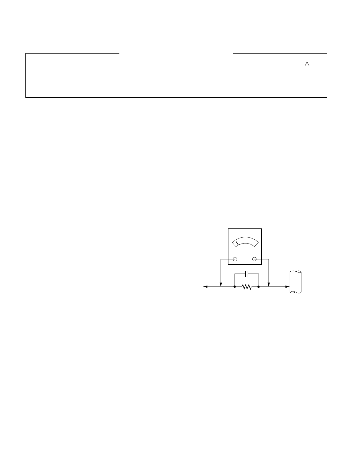
Leakage Current Hot Check (See below Figure)
Plug the AC cord directly into the AC outlet.
Do not use a line Isolation Transformer during this check.
Connect 1.5K/10watt resistor in parallel with a 0.15uF capacitor
between a known good earth ground (Water Pipe, Conduit, etc.)
and the exposed metallic parts.
Measure the AC voltage across the resistor using AC voltmeter
with 1000 ohms/volt or more sensitivity.
Reverse plug the AC cord into the AC outlet and repeat AC voltage
measurements for each exposed metallic part. Any voltage
measured must not exceed 0.75 volt RMS which is corresponds to
0.5mA.
In case any measurement is out of the limits specified, there is
possibility of shock hazard and the set must be checked and
repaired before it is returned to the customer.
Leakage Current Hot Check circuit
IMPORTANT SAFETY NOTICE
0.15uF
To Instrument's
exposed
METALLIC PARTS
AC Volt-meter
Good Earth Ground
such as WATER PIPE,
CONDUIT etc.
1.5 Kohm/10W

- 4 -
CAUTION: Before servicing receivers covered by this service
manual and its supplements and addenda, read and follow the
SAFETY PRECAUTIONS on page 3 of this publication.
NOTE: If unforeseen circumstances create conflict between the
following servicing precautions and any of the safety precautions on
page 3 of this publication, always follow the safety precautions.
Remember: Safety First.
General Servicing Precautions
1. Always unplug the receiver AC power cord from the AC power
source before;
a. Removing or reinstalling any component, circuit board
module or any other receiver assembly.
b. Disconnecting or reconnecting any receiver electrical plug or
other electrical connection.
c. Connecting a test substitute in parallel with an electrolytic
capacitor in the receiver.
CAUTION: A wrong part substitution or incorrect polarity
installation of electrolytic capacitors may result in an
explosion hazard.
2. Test high voltage only by measuring it with an appropriate high
voltage meter or other voltage measuring device (DVM,
FETVOM, etc) equipped with a suitable high voltage probe.
Do not test high voltage by "drawing an arc".
3. Do not spray chemicals on or near this receiver or any of its
assemblies.
4. Unless specified otherwise in this service manual, clean
electrical contacts only by applying the following mixture to the
contacts with a pipe cleaner, cotton-tipped stick or comparable
non-abrasive applicator; 10% (by volume) Acetone and 90% (by
volume) isopropyl alcohol (90%-99% strength)
CAUTION: This is a flammable mixture.
Unless specified otherwise in this service manual, lubrication of
contacts in not required.
5. Do not defeat any plug/socket B+ voltage interlocks with which
receivers covered by this service manual might be equipped.
6. Do not apply AC power to this instrument and/or any of its
electrical assemblies unless all solid-state device heat sinks are
correctly installed.
7. Always connect the test receiver ground lead to the receiver
chassis ground before connecting the test receiver positive
lead.
Always remove the test receiver ground lead last.
8. Use with this receiver only the test fixtures specified in this
service manual.
CAUTION: Do not connect the test fixture ground strap to any
heat sink in this receiver.
Electrostatically Sensitive (ES) Devices
Some semiconductor (solid-state) devices can be damaged easily
by static electricity. Such components commonly are called
Electrostatically Sensitive (ES) Devices. Examples of typical ES
devices are integrated circuits and some field-effect transistors and
semiconductor "chip" components. The following techniques
should be used to help reduce the incidence of component
damage caused by static by static electricity.
1. Immediately before handling any semiconductor component or
semiconductor-equipped assembly, drain off any electrostatic
charge on your body by touching a known earth ground.
Alternatively, obtain and wear a commercially available
discharging wrist strap device, which should be removed to
prevent potential shock reasons prior to applying power to the
unit under test.
2. After removing an electrical assembly equipped with ES
devices, place the assembly on a conductive surface such as
aluminum foil, to prevent electrostatic charge buildup or
exposure of the assembly.
3. Use only a grounded-tip soldering iron to solder or unsolder ES
devices.
4. Use only an anti-static type solder removal device. Some solder
removal devices not classified as "anti-static" can generate
electrical charges sufficient to damage ES devices.
5. Do not use freon-propelled chemicals. These can generate
electrical charges sufficient to damage ES devices.
6. Do not remove a replacement ES device from its protective
package until immediately before you are ready to install it.
(Most replacement ES devices are packaged with leads
electrically shorted together by conductive foam, aluminum foil
or comparable conductive material).
7. Immediately before removing the protective material from the
leads of a replacement ES device, touch the protective material
to the chassis or circuit assembly into which the device will be
installed.
CAUTION: Be sure no power is applied to the chassis or circuit,
and observe all other safety precautions.
8. Minimize bodily motions when handling unpackaged
replacement ES devices. (Otherwise harmless motion such as
the brushing together of your clothes fabric or the lifting of your
foot from a carpeted floor can generate static electricity
sufficient to damage an ES device.)
General Soldering Guidelines
1. Use a grounded-tip, low-wattage soldering iron and appropriate
tip size and shape that will maintain tip temperature within the
range or 500
F to 600 F.
2. Use an appropriate gauge of RMA resin-core solder composed
of 60 parts tin/40 parts lead.
3. Keep the soldering iron tip clean and well tinned.
4. Thoroughly clean the surfaces to be soldered. Use a mall wirebristle (0.5 inch, or 1.25cm) brush with a metal handle.
Do not use freon-propelled spray-on cleaners.
5. Use the following unsoldering technique
a. Allow the soldering iron tip to reach normal temperature.
(500
F to 600 F)
b. Heat the component lead until the solder melts.
c. Quickly draw the melted solder with an anti-static, suction-
type solder removal device or with solder braid.
CAUTION: Work quickly to avoid overheating the
circuitboard printed foil.
6. Use the following soldering technique.
a. Allow the soldering iron tip to reach a normal temperature
(500
F to 600 F)
b. First, hold the soldering iron tip and solder the strand against
the component lead until the solder melts.
c. Quickly move the soldering iron tip to the junction of the
component lead and the printed circuit foil, and hold it there
only until the solder flows onto and around both the
component lead and the foil.
CAUTION: Work quickly to avoid overheating the circuit
board printed foil.
d. Closely inspect the solder area and remove any excess or
splashed solder with a small wire-bristle brush.
SERVICING PRECAUTIONS

- 5 -
IC Remove/Replacement
Some chassis circuit boards have slotted holes (oblong) through
which the IC leads are inserted and then bent flat against the
circuit foil. When holes are the slotted type, the following technique
should be used to remove and replace the IC. When working with
boards using the familiar round hole, use the standard technique
as outlined in paragraphs 5 and 6 above.
Removal
1. Desolder and straighten each IC lead in one operation by gently
prying up on the lead with the soldering iron tip as the solder
melts.
2. Draw away the melted solder with an anti-static suction-type
solder removal device (or with solder braid) before removing the
IC.
Replacement
1. Carefully insert the replacement IC in the circuit board.
2. Carefully bend each IC lead against the circuit foil pad and
solder it.
3. Clean the soldered areas with a small wire-bristle brush.
(It is not necessary to reapply acrylic coating to the areas).
"Small-Signal" Discrete Transistor
Removal/Replacement
1. Remove the defective transistor by clipping its leads as close as
possible to the component body.
2. Bend into a "U" shape the end of each of three leads remaining
on the circuit board.
3. Bend into a "U" shape the replacement transistor leads.
4. Connect the replacement transistor leads to the corresponding
leads extending from the circuit board and crimp the "U" with
long nose pliers to insure metal to metal contact then solder
each connection.
Power Output, Transistor Device
Removal/Replacement
1. Heat and remove all solder from around the transistor leads.
2. Remove the heat sink mounting screw (if so equipped).
3. Carefully remove the transistor from the heat sink of the circuit
board.
4. Insert new transistor in the circuit board.
5. Solder each transistor lead, and clip off excess lead.
6. Replace heat sink.
Diode Removal/Replacement
1. Remove defective diode by clipping its leads as close as
possible to diode body.
2. Bend the two remaining leads perpendicular y to the circuit
board.
3. Observing diode polarity, wrap each lead of the new diode
around the corresponding lead on the circuit board.
4. Securely crimp each connection and solder it.
5. Inspect (on the circuit board copper side) the solder joints of
the two "original" leads. If they are not shiny, reheat them and if
necessary, apply additional solder.
Fuse and Conventional Resistor
Removal/Replacement
1. Clip each fuse or resistor lead at top of the circuit board hollow
stake.
2. Securely crimp the leads of replacement component around
notch at stake top.
3. Solder the connections.
CAUTION: Maintain original spacing between the replaced
component and adjacent components and the circuit board to
prevent excessive component temperatures.
Circuit Board Foil Repair
Excessive heat applied to the copper foil of any printed circuit
board will weaken the adhesive that bonds the foil to the circuit
board causing the foil to separate from or "lift-off" the board. The
following guidelines and procedures should be followed whenever
this condition is encountered.
At IC Connections
To repair a defective copper pattern at IC connections use the
following procedure to install a jumper wire on the copper pattern
side of the circuit board. (Use this technique only on IC
connections).
1. Carefully remove the damaged copper pattern with a sharp
knife. (Remove only as much copper as absolutely necessary).
2. carefully scratch away the solder resist and acrylic coating (if
used) from the end of the remaining copper pattern.
3. Bend a small "U" in one end of a small gauge jumper wire and
carefully crimp it around the IC pin. Solder the IC connection.
4. Route the jumper wire along the path of the out-away copper
pattern and let it overlap the previously scraped end of the good
copper pattern. Solder the overlapped area and clip off any
excess jumper wire.
At Other Connections
Use the following technique to repair the defective copper pattern
at connections other than IC Pins. This technique involves the
installation of a jumper wire on the component side of the circuit
board.
1. Remove the defective copper pattern with a sharp knife.
Remove at least 1/4 inch of copper, to ensure that a hazardous
condition will not exist if the jumper wire opens.
2. Trace along the copper pattern from both sides of the pattern
break and locate the nearest component that is directly
connected to the affected copper pattern.
3. Connect insulated 20-gauge jumper wire from the lead of the
nearest component on one side of the pattern break to the lead
of the nearest component on the other side.
Carefully crimp and solder the connections.
CAUTION: Be sure the insulated jumper wire is dressed so the
it does not touch components or sharp edges.
- 6 -
SPECIFICATION
NOTE : Specifications and others are subject to change without notice for improvement
.
1.General Specification(TV)
No Item Specification Remark
1. Video input applicable system PAL-D/K, B/G, I, NTSC-M, SECAM
NTSC 4.43
2. Receivable Broadcasting System 1) PAL/SECAM BG (ZE/TE)
2) PAL/SECAM DK EU/Non-EU
3) PAL I/I (PAL Market)
4) SECAM L/L'
5) NTSC M
6) PAL-N/M 6),7) South America Market
7) NTSC M
7) Except South America NTSC Market (ME)
3. RF Input Channel VHF : E2 ~ E12 PAL
UHF : E21 ~ E69
CATV : S1 ~ S20
HYPER : S21~ S47
L/L' : B, C, D FRANCE
VHF : 2~13 NTSC
UHF : 14~69
CATV : 1~125
VHF Low : 1 ~ M10 JAPAN
VHF High : 4~S22
UHF : S23~62
4. Input Voltage AC 100 ~ 240 V/50Hz, 60Hz
5. Market Worldwide
6. Picture Size 1067.308mm 42.02inch(42LB1R)
7. Tuning System FVS 100 program PAL, 200 PR.(Option)
FS NTSC
8. Operating Environment 1) Temp : 0 ~ 40 deg
2) Humidity : 10~90 %
9. Storage Environment 3) Temp : -20 ~ 50 deg
4) Humidity : 10~90 %
10. Display LCD Module LPL
- 7 -
2. General Specification
No Item Specification Remark
1 Panel 42" TFT WXGA LCD
2 Frequency range H : 31 ~ 61Khz PC Input
V : 56 ~ 75Hz
3 Control Function 1) Contrast/Brightness
2) H-Position / V-Position
3) Tracking : Clock / Phase
4) Auto Configure
5) Reset
4 Component Jack 1 : Y Middle east / NTSC Area
3 : Pb
5 : Pr
7 : Line1 Ready
9 : LINE2
11: LINE3
13: Line3 Ready
D4 Jack(525i, 525p, 750p,1125i) 2 : Y GND JAPAN Only
4 : Pb GND
6 : Pr GND
8 : LINE1
10:Line2 Ready
12:SWITCH GND
14: SWITCH
5 H/V-Sync Video Power consumption LED
Power ON - -
≤ 240W
Stand by
≤ 3.0W
Red
DPMS Mode ON/OFF OFF
≤ 30W
Green
Power off - - - *
6 LCD Module Outline 42"
1006 x 610 x 56(mm)
(H)x(V)x(D)
Dimension
Pixel Pitch 42"
0.227 x 0.681 x RGB(mm)
Pixel Format 1366 horiz. By 768 vert.
Pixels RGB strip arrangement
Coating Hard coating(3H), Anti-glare
reatment of the front polarizer,
Back Light 42" 20EEFL
- 8 -
3.Optical Feature(LCD Module)
Item RemarkSpecification
Viewing Angle<CR
10>
Luminance
Contrast Ratio
CIE Color Coordinates
Typical
MAX/MIN
ALL white/All back
LPL
R/L, U/D
Luminance(cd/
)
Variation
CR
CR
D (With Al)
Typ
176, 176
500
400
1000
0.285
0.293
0.640
0.341
0.287
0.610
0.146
0.069
WHITE
RED
GREEN
BLUE
W
x
W
y
R
R
y
G
x
G
y
B
x
B
y
Typ.
Typ.
Typ.
Typ.
Typ.
Typ.
Typ.
Typ.
No.
1
2
3
4
4.Component Video Input (Y, PB, PR)
No
Specification
Proposed
Resolution H-freq(kHz) V-freq(Hz)
1. 640x480 15.73 60 SDTV, DVD 480i ZE, TE, ME
2. 640x480 15.63 59.94 SDTV, DVD 480i ZE, TE, ME
3. 720x480 31.47 59.94 EDTV 480p TE, ME
4. 720x576 15.625 50.00 SDTV, DVD 625 Line ZE, TE, ME
5. 720x576 31.25 50.00 HDTV 576p TE, ME
6. 1280x720 45.00 60.00 HDTV 720p TE, ME
7. 1280x720 44.96 59.94 HDTV 720p TE, ME
8. 1920x1080 31.25 50.00
HDTV 1080i 50Hz (AU Ver.)
TE, ME
9. 1920x1080 33.75 60.00
HDTV 1080i 60Hz (ATSC)
TE, ME
10. 1920x1080 33.72 59.94 HDTV 1080i 59.94Hz TE, ME
5. RGB PC INPUT Mode Table
No Resolution H-freq(kHz) V-freq.(Hz) Pixel clock(MHz) Proposed
Analog RGB, Digital RGB
1 720x400 31.468 70.8 28.321
2 640x480 31.469 59.94 25.17 VESA
37.684 75.00 31.5 VESA
3 800x600 37.879 60.31 40.00 VESA
46.875 75 49.5 VESA
4 832x624 49.725 74.55 57.283
5 1024x768 48.363 60.00 65.00 VESA(XGA)
56.47 70.00 75.00 VESA(XGA)
60.123 75.029 78.75 VESA(XGA)
6 1280x768 47.776 59.870 79.50 VESA(WXGA)
7 1360x768 47.720 59.799 84.75 VESA(WXGA)
8 1366x768 47.720 59.799 84.75 Supported
Min
300
700
Typ.
-0.03
Max
1.3
Typ.
+0.03
- 9 -
No Resolution H-freq(kHz) V-freq.(Hz) Pixel clock(MHz) Proposed
1 720x576 31.25 50.00 SDTV 576p 50Hz
2 720x480 31.47 59.94 SDTV 480p 60Hz
3 1280x720 45.00 50.00 HDTV 720p 50Hz HDCP
4 1280x720 44.96 59.94 HDTV 720p 60Hz HDCP
5 1920x1080 28.13 50.00 HDTV 1080i 50Hz HDCP
6 1920x1080 33.72 59.94 HDTV 1080i 60Hz HDCP
6. RGB DTV INPUT Mode Table
No Resolution H-freq(kHz) V-freq.(Hz) Pixel clock(MHz) Proposed
1 720x576 31.25 50.00 SDTV 576p 50Hz
2 720x480 31.47 59.94 SDTV 480p 60Hz
3 1280x720 45.00 50.00 HDTV 720p 50Hz HDCP
4 1280x720 44.96 59.94 HDTV 720p 60Hz HDCP
5 1920x1080 28.13 50.00 HDTV 1080i 50Hz HDCP
6 1920x1080 33.72 59.94 HDTV 1080i 60Hz HDCP
8. HDMI DTV INPUT Mode Table
7. HDMI PC INPUT Mode Table
No Resolution H-freq(kHz) V-freq.(Hz) Pixel clock(MHz) Proposed
Analog RGB, Digital RGB
1 720x400 31.468 70.8 28.321
2 640x480 31.469 59.94 25.17 VESA
37.684 75.00 31.5 VESA
3 800x600 37.879 60.31 40.00 VESA
46.875 75 49.5 VESA
4 832x624 49.725 74.55 57.283
5 1024x768 48.363 60.00 65.00 VESA(XGA)
56.47 70.00 75.00 VESA(XGA)
60.123 75.029 78.75 VESA(XGA)
6 1280x768 47.776 59.870 79.50 VESA(WXGA)
7 1360x768 47.720 59.799 84.75 VESA(WXGA)
8 1366x768 47.720 59.799 84.75 Supported
9 1920x1080 33.75 60.00 86.375 HDCP DVI Digital 1080i
10 1280x720 45.00 60.00 74.375 HDCP DVI Digital 720p
9. Mechanical specification
No, Item Content Remark
1 Product Dimenson Width(W) Length(D) Height(H)
Before Packing 1175 300 768 With Stand
After Packing 1282 386 920
2 Product Weight Only SET 43.4Kg With Stand
With Box 48.2kg
- 10 -
10. Mechanical specification
<Table 1> Scart Arrangement 1.(Full Scart)
Pin Signal Signal Level Impedance
1 Audio Output B (right) 0.5 Vrms < 1
2 Audio Input B (right) 0.5 Vrms > 10
3 Audio Output A (left) 0.5 Vrms < 1
4 Ground (audio) - 5 Ground (blue) - 6 Audio input A (left) 0.5 Vrms > 10
7 Blue input 0.7 V 75
8 Function Select (AV control) High (9.5 - 12V) - AV Mode
Mid (5 - 8V) - Wide Screen > 10
Low (0 - 2V) - TV Mode
9 Ground (Green) - 10 Comms Data 2
11 Green input 0.7 V 75
12 Comms Data 1
13 Ground (Red) - 14 Ground (Blanking) - 15 Red input 0.7 V 75
16 RGB Switching Control High (1 - 3V) - RGB
Low (0 - 0.4V) - Composite 75
17 Ground (Video input & Output) - 18 Ground (RGB Switching Control) - 19 Video output (Composite) 1V including sync 75
20 Video input (Composite) 1V including sync 75
21 Common ground (Shield) - -
<Table 2> Scart Arrangement 2.(Half Scart)
Pin Signal Signal Level Impedance
1 Audio Output B (right) 0.5 Vrms < 1
2 Audio Input B (right) 0.5 Vrms > 10
3 Audio Output A (left) 0.5 Vrms < 1
4 Ground (audio) - 5 Ground (blue) - 6 Audio input A (left) 0.5 Vrms > 10
7- - 8 Function Select (AV control) High (9.5 - 12V) - AV Mode
Mid (5 - 8V) - Wide Screen > 10
Low (0 - 2V) - TV Mode
9 Ground (Green) - 10 Comms Data 2
11 - - 12 Comms Data 1
13 Ground (Red) - 14 Ground (Blanking) - 15 Red input
16 - - 17 Ground (Video input & Output) - 18 - - 19 Video output (Composite) 1V including sync 75
20 Video input (Composite) 1V including sync 75
21 Common ground (Shield) - -
- 11 -
ADJUSTMENT INSTRUCTION
1. Application Object
These instructions are applied to all of the PDP TV, PA61A.
2. Notes
(1) Because this is not a hot chassis, it is not necessary to use
an isolation transformer. However, the use of isolation
transformer will help protect test equipment.
(2) Adjustments must be done in the correct order.
(3) The adjustments must be performed in the circumstance of
25±5°C of temperature and 65±10% of relative humidity if
there is no specific designation.
(4) The input voltage of the receiver be must kept 110V, 60Hz
when adjusting.
(5) The receiver must be operational for about 15 minutes
prior to the adjustments.
O Preliminary action is applied to the test for afterimage
discharge detection, and 100% FULL WHITE PATTERN
must be operated automatically.
O Test for afterimage discharge detection
1) After pressing Power Only key(only operating by
pressing Power Only key), Full Test Pattern(2 min
30sec) --> Full Black Pattern(30sec) --> After this state,
Full White Pattern is displayed.
(but you must preset the program for Full White State
when you press the Main Power Off/On)
2) Pattern Mode is deselected by pressing CH +/-, Exit Key.
[ Set is activated HEAT-RUN without signal generator in this
mode.
3. EPLD Download
(1) Test Equipment: PC, Jig for download
(2) Connect the power of VSC B/D.
(3) Execute download program(iMPACK) of PC.
(4) After executing the hot key on the Programmer, click icon
(5) End after confirming
4. Gemstar VBI Micom Download
4-1. Preparation for Adjustment
(1) As shown below, connect the MPLAB ICD2 equipment, PC
and Digital Connector.
(2) Turn on the MPLAB ICD2 POWER Supply.
(3) After turn on the PC and MONITOR, select the ‘MPLAB
IDE’ from the screen.
4-2. Adjustment Sequence
(1) When the program is executed, select the MPLAB ICD2
from Programmer -> Select Programmer .
If you turn on a still screen more than 20 minutes (Especially
Digital pattern(13 CH), Cross Hatch Pattern), an afterimage
may occur in the black level part of the screen.
PC
VSC
B/D
+13V
GND
Data
Test Pattern 2min 30sec
Test Pattern 30sec
Connect the RS-232 or USB Cable
Connect the MPLAB ICD2 and connector of Digital Board
<Digital Board>
- 12 -
(2) Select "Configure -> Select Device".
(3) When the "Select Device" window appears, select the
PIC18F1220 from "Device" and press OK.
(4) Select "Programmer -> Connect".
When connected with the Micom, the display message on
the Output window appears as below.
(5) Select "File -> Import", select the Work HEX file and open.
(6) Select "Programmer -> Program".
(7) Download is executed and about 5 seconds later, the
"Programming succeeded" message is displayed on the
Output window and the Download process is ended.
(8) The execution of process (6) is convenient when using the
short-cut icon.
5. POD Certificate Download
5-1. Preparation for Adjustment
(1) Connect the MEMORY JIG and PC.
(2) Turn on the JIG MAIN POWER SWITCH.
(3) After turn on the PC and MONITOR, execute the
‘Certificate Downloader v1.4’ from the screen.
5-2. Adjustment Sequence
(1) After open the ‘Certificate Downloader v1.4’, enter
Connection set and set the as same below.
The port settings are determined by each PC's setup.
(2) Select ‘Connection’ and SET connected to RS-232C.
(3) After clicking "Enter", confirm that "Enter Password:"
appears.
- 13 -
(4) Click the "OpenFile - Download" button from CP Data
Download, ‘select the Private Key’ appears and click
ENTER.
(5) After clicking ENTER, the ‘opens Private key' window
appears and select the Private key applied to the SET.
The Private Key file name is on the Label of the Digital
Board.
(6) When the Dialog window appears, click OK and the write
work will begin.
(7) When completed, click ‘CP Data Download: OK’
[ When ‘CP Data Download: OK’ does not appear, certificate
has not Download correctly.
SET is rebooted and certificate Download work must be
repeated.
6. Gemstar Operation Confirmation
6-1. Required Test Equipment
(1) PC with Factory Test Program
(2) VBI Inserter (Norpak TES3) - Guide Data Discharge
Equipment
[ In case of without the VBI Inserter(TES3), a VCR may be
used.
6-2. Preparation for Adjustments
(1) In case of with VBI Inserter(TES3): Signal uses Cable input
and set as below.
(2) In case of without VBI Inserter(TES3): VCR uses Cable
input and set as below.
[ Factory Test S/W must be set to "GlinkTo PC Card" ON.
6-3. Adjustment Confirmation Work
(1) Turn on the TV and run Factory Test Program of PC.
[ Program only needs to run once, regardless of set quantity.
(2) Enter the EZ adjust menu by pressing Adjust on the
Service Remote Control (S R/C).
(3) Go to number 1 Gemstar and press Enter.
(4) TV set screen will appear as shown.
(5) Confrim that VBI Test and Serial Test PASS from the
screen.
RS-232C
Input Signal
7. Cable Operation Confirmation
(1) Confirm that the Cable Card is inserted in the slot.
(2) Enter the EZ adjust menu by pressing the Adjust key on
the Service Remote Control (S R/C).
(3) Go to number 2 Cable Check and press the Right key (
G ) .
(4) Confirm items below.
8. POWER PCB Assy Voltage
Adjustment
(Va, Vs Voltage Adjustment)
8-1. Test Equipment :D.M.M 1EA
8-2. Connection Diagram for Measuring
Refer to Fig 1.
9. EDID(The Extended Display
Identification Data)/DDC
(Display Data Channel) Download
This is the function that enables “Plug and Play".
9-1. HDMI EDID Data Input
(1) Required Test Equipment
1) PC, Jig for adjusting DDC. (PC serial to D-sub
Connection equipment)
2) S/W for writing DDC(EDID data write & read)
3) D-Sub cable
4) Jig for HDMI Cable connection
(2) Preparation for Adjustments &
Setting of Device
1) Set devices as below and turn on the PC and JIG.
2) Open S/W for writing DDC (EDID data write & read).
(operated in DOS mode)
- 14 -
Name
Descrambler
Check
CableCARD
OOB Path
FDC_SNR
Video Signal
Normal
OK
CableCARD
TM
is inserted.
OK(Lock)
OK(20dB above)
Normal Screen
Defective
Not OK
CableCARD
TM
is removed.
Not OK(Unlock)
Not OK(20dB under)
Black Screen
(No Picture)
Each PCB Assy must be checked by Check JIG Set before
assembly. (Especially, be careful Power PCB Assy which can
cause Damage to the PDP Module.)
<Fig. 1-1> Connection Diagram of Power Adjustment for
Measuring (Power Board): 50”
<Fig. 2>
<Fig. 1-2> Connection Diagram of Power Adjustment for
Measuring (Power Board): 60”
Vs
GND
Va
DMM
P805
GND
5V
-+
P804
P800
Vs
AD
AD
Va
VR95 VR90
P803
1
P802
1
1
PDP TV SET
(or Digital Board)
CN1
10. ADC-Set Adjustment
10-1. Synopsis
ADC-Set adjustment to set the black level and the Gain to
optimum.
10-2. Test Equipment
Service R/C, 801GF(802B, 802F, 802R) or MSPG925FA
Pattern Generator
(720P The Horizontal 100% Color Bar Pattern output will be
possible and the output level will accurately have to be
revised with 0.7±0.1Vp-p)
10-3. Adjustment
(1) ADC 480i Component1 Adjustment
Check the connection Component1 to the Test Equipment
(1) Select Component1 as the input with 100% Horizontal
Color Bar Pattern(HozTV31Bar) in 480i Mode and
select ‘Normal’ in screen.
(2) After receiving signal for at least 1 second, press the
ADJ Key on the Service R/C to enter the ‘Ez - Adjust’
and select the ‘4. ADC 480i Comp1’.
Pressing the Enter Key to adjust with automatic
movement.
(3) When the adjustment is over, 'ADC Component1
Success’ is displayed.
(4) If the adjustment has errors, 'ADC Configuration Error’
is displayed. And error massage(‘Component Not
Connection’ or ‘Change Format to 480i’ or ‘Check
Pattern of device’ ) is displayed for 1 second.
(2) ADC 1080i Component2/RGB Adjustment
Check the connection Component2, RGB to the Test
Equipment
(1) Select Component2 as the input with 100% Horizontal
Color Bar Pattern(HozTV31Bar) in 1080i Mode and
select ‘Normal’ in screen.
(2) After receiving signal for at least 1 second, press the
ADJ Key on the Service R/C to enter the ‘Ez - Adjust’
and select the ‘5. ADC 480p Comp2/RGB’.
Pressing the Enter Key to adjust with automatic
movement.
(3) When the adjustment is over, 'ADC Component2
Success’ is displayed. If the adjustment has errors,
'ADC Configuration Error’ is displayed.
(4) After the Component2 adjustment is over, convert the
RGB-DTV Mode and display Pattern.
When the adjustment is over, 'ADC RGB_DTV Success’
is displayed.
(5) Readjust after confirming the case Pattern or
adjustment condition where the adjustment errors.
Error massage is ‘Component Not Connection’ or
‘Change Format to 480i’ or ‘Check Pattern of device’.
(6) After adjustment is complete, exit the adjustment mode
by pressing the ADJ KEY.
11. Adjustment of White Balance
11-1. Connection Diagram of Equipment
for Measuring (Automatic Adjustment)
[ RS-232C Command (Automatic Adjustment)
- 15 -
<Fig. 4> Connection Diagram of Automatic Adjustment
R Gain
G Gain
B Gain
R Cut
G Cut
B Cut
Jg
Jh
Ji
Cool
Ja
Jb
Jc
Mid
RS-232C COMMAND
[CMD ID DATA]
CENTER
(DEFAULT)
Jd
Je
Jf
00
00
00
255
255
255
127
127
127
Warm
Min Max
184
187
192
64
64
64
Cool
161
183
192
64
64
64
Mid
192
159
95
64
64
64
Warm
<Fig. 3> Adjustment Pattern : 480i/1080i 60Hz HozTV31
Bar Pattern
Full White Pattern
COLOR
ANALYZER
TYPE; CA-100
Digital RGB
PDP MONITOR
MSPG-925FA
11-2. Adjustment of White Balance
O
Operate the Zero-calibration of the CA-210, then attach
sensor to PDP module surface when you adjust.
O
Manual adjustment is also possible by the following sequence.
(1) HEAT RUN at least 30 minutes by pressing the Power only
Key on the Service Remote Control and adjust.
(2) After attaching sensor to center of screen, select ‘White-
Balance’ of ‘Ez - Adjust’ by pressing the ADJ KEY on the
Service R/C. Then enter adjustment mode by pressing the
Right KEY (
G
). This time white pattern is displayed.
(3) Adjust the Hight Light using R Gain/G Gain(Cool).
Adjust the Hight Light using G Gain/R Gain(Medium).
Adjust the Hight Light using G Gain/B Gain(Warm).
(R Gain: 192, B Gain 192, R-Cut/G-Cut/B-Cut: 64 Fix.)
(4) Adjust using Volume +/- KEY.
(5) After adjustment is complete, exit the adjustment mode by
pressing the ADJ KEY.
High Level: 216gray
[Cool]
X; 0.278±0.015 Y; 0.279±0.015
Color temperature: 11000°K±1000°K
dUV: -3dUV
[Medium]
X; 0.287±0.015 Y; 0.289±0.015
Color temperature: 9300°K±1000°K
dUV: -3dUV
[Warm]
X; 0.314±0.015 Y; 0.318±0.015
Color temperature: 6500°K±1000°K
dUV: -3dUV
12. Video(uPD)-Set
Adjustment for reduce color difference Main/Sub screen of RF
or Video signal.
12-1. Adjustment
(1) Connection the Video Signal Generator(Master) to the TV
AV Input terminal.
After input pattern(Model: 201(NTSC-M), Pattern: 32(100%
color Bar), pressing the ‘Rev’ button and appear as below
figure
(2) After receive signal, confirm the signal receiving.
And Enter the ‘EZ-ADJUST’ by pressing the ADJ Key on
the Service R/C.
Select ‘5. Video(UPD)-Set’ and enter the adjustment mode
by pressing the right key (
G
).
(3) When enter the adjustment mode, displayed the TV 2CH
SPLIT Screen automatic at picture and appear as below
figure.
(4) When the automatic adjustment is over, 'RF Configuration
Success’ is displayed. If the adjustment has errors, 'Video
Configuration Error’ is displayed.
(5) After the RF signal automatic adjustment is over, convert
the Video Mode as below figure and adjust with automatic
movement the Video Mode.
When the automatic adjustment is over, 'Video
Configuration Success’ is displayed. If the adjustment has
errors, 'Video Configuration Error’ is displayed.
- 16 -
- 17 -
SVC REMOCON
1 POWER
2 POWER ON
3 MUTE
4 P-CHECK
5 S-CHECK
6 ARC
7 CAPTION
8 TXT
9 TV/AV
10 TURBO SOUND
11 TURBO PICTURE
12 IN-START
13 ADJ
14 MPX
15 EXIT
16 APC(PSM)
17 ASC(SSM)
18 MULTIMIDIA
19 FRONT-AV
20 CH
21 VOL
22 ENTER
23 PIP CH-(OP1)
24 PIP CH+(OP2)
25 PIP SWAP(OP3)
26 PIP INPUT(OP4)
27 EYE
28 MENU
29 IN-STOP
30 STILL
31 TIME
32 SIZE
33 MULTI PIP
34 POSITION
35 MODE
36 PIP
37 TILT
38 0~9
To turn the TV on or off
To turn the TV on automatically if the power is supplied to the TV. (Use the
POWER key to deactivate): It should be deactivated when delivered.
To activate the mute function.
To check TV screen image easily.
To check TV screen sound easily
To select size of the main screen (Normal, Spectacle, Wide or Zoom)
Switch to closed caption broadcasting
To toggle on/off the teletext mode
To select an external input for the TV screen
To start turbo sound
To start turbo picture
To enter adjustment mode when manufacturing the TV sets.
To adjust the screen voltage (automatic):
In-start
mute Adjust AV(Enter into W/B adjustment mode)
W/B adjustment (automatic):
After adjusting the screen W/B adjustment Exit two times (Adjustment completed)
To enter into the adjustment mode. To adjust horizontal line and sub-brightness.
To select the multiple sound mode (Mono, Stereo or Foreign language)
To release the adjustment mode
To easily adjust the screen according to surrounding brightness
To easily adjust sound according to the program type
To check component input
To check the front AV
To move channel up/down or to select a function displayed on the screen.
To adjust the volume or accurately control a specific function.
To set a specific function or complete setting.
To move the channel down in the PIP screen.
To use as a red key in the teletext mode
To move the channel in the PIP screen
To use as a green key in the teletext mode
To switch between the main and sub screens
To use as a yellow key in the teletext mode
To select the input status in the PIP screen
To use as a blue key in the teletext mode
To set a function that will automatically adjust screen status to match
the surrounding brightness so natural color can be displayed.
To select the functions such as video, voice, function or channel.
To set the delivery condition status after manufacturing the TV set.
To halt the main screen in the normal mode, or the sub screen at the PIP screen.
Used as a hold key in the teletext mode (Page updating is stopped.)
Displays the teletext time in the normal mode
Enables to select the sub code in the teletext mode
Used as the size key in the PIP screen in the normal mode
Used as the size key in the teletext mode
Used as the index key in the teletext mode (Top index will be
displayed if it is the top text.)
To select the position of the PIP screen in the normal mode
Used as the update key in the teletext mode (Text will be
displayed if the current page is updated.)
Used as Mode in the teletext mode
To select the simultaneous screen
To adjust screen tilt
To manually select the channel.
Shortcut keys
Shortcut keys
Shortcut keys
Use the AV
key to enter
the screen
W/B
adjustment
mode.
Shortcut keys
Shortcut keys
Shortcut keys
- 18 -
VIDEO TROUBLESHOOTING & BLOCK DIAGRAM
r
r
r
3
r
• DCR DVR
12
LVDS Tx.
RGB
(THC63LVD103)
DOutClk
30
SPDIF
Control GPIO
Peripheral Bus
MST33611_HDMI
SPDIF_IN_BYPASS
CPLD
System
HD2_ICE958_OUT
HDMI_SPDIF
HD2_DAC_SCK/LRCK
4
4
) *2
IIC3
0x12
TX/RX P2,N2
TX/RX P1,N1
,TPB r
X-tal
(TPA r
(25M)
LGDPLL
(SiI3512)
SATA I/F
1394
Controll er
(TSB43DA42)
(LGDT1901B)
HD2_SYS_CLK
DPLL_R[1:3]
(74.25M)
HD2_VDPClk
CXA2069
XDR_DATA_R/G/B[0:9]
HD2_REC_CVBS
TX[0:4]±
TXC±
IEP3
IIC2
0x1E
HV,Hact
CY2305SC
(CS8415A)
VCXO
(8MB x4)
SDRAM
32MByte
(LGDT1303)
VPP1
VPP
0xB8
IIC 2
V/Q _TP
IIC 2
0xB2
X-tal
(25M)
V
V
Video In/Out
Video In/Out
z
27Mh
64-Bit I/F
1.8V
656 Data[0:7]
SDRAM
X-tal
IN5
TV
IN1
V, LR
3
Rear AV_ 1
Reg.
TP/D1
HD2_TP[0:7]
(1Mx 16Bit)
(24.576M)
2
YC
Rear S_1
HD2_MAIN_PWM
8
CP_656[0-7]
MUX
CPLD
Video Dec oder
2
Filter(opt)
(FMS6410)
(Sub)
OUT2
IN1
2
EPF_L/R
HD-2.4
Sub
MSP4458G
CP_656_CLK
SEL
PDR 656[0:7]
(UPD64015)
A/V SW
(CXA2069)
IN3
IN6
V,LR
Side AV_ 2
HD2_CVBS_OUT
HD-II
-TP De-Mux
- MPEG Decodi ng : MP@HL
-Format Converter
EXT_IN_CLK
SUB_656_CLK
CY2309
SYS
CPLD
656CLK
SDRAM
X-tal
IIC 2
0xBA
2
IIC 3
Filter(opt)
(FMS6410)
2
OUT1
(Main)
IN4
IN4
YC
3
2
Side S_2
MNT_V_Out
-Host I/F, Memory I/F
YCbCr
30
OR1
YCbCr
(1Mx 16Bit)
(24.576M)
0x50
IIC 4
OUT3
-Digital I/F
-NTSC Encod er
H,V
CPLD
OR3
H,V
2
CLK
20
(UPD64015)
Video Dec oder
uCom
MTV416
0x90
OUT1
LR
2
AV_L/R_OUT
4440
M_MSP
FID
-AC-3 Decod er/SPDIF In/out
OR2
FID
P_SW_2
YCbCr
Comp_1
-IEP2
OR1
YCbCr
30
IIC 4
IN4
3
0x84
AH_SPDIFCLK
VBI Slicer & IR (USA Only)
CPLD
OR2
OR3
H,V
FID
CLK
2
ADC
(MST3361)
LPF(OPT)
(FMS6403)
YCbCr
3
Video SW
IN1
(CXA2181)
IN2
IN3
YCbCr
RGBHV
3
Comp_2
RGB-PC
5
HD2_NT2CLK
PVR_SYS_CLK
EPLD_CLK
• Block Box-show the
IN/OUT connections
PCI Bus
1394_IN_TP[0:7]
1394_OUT_TP[0:7]
MUX
CPLD
2
11
VPP_SW
VPP_SW
POD_TP[0:7]
VSB DATA
OOB/POD Controller (USA Only)
(6M)
IF r
OOB IF+/-
nd
2
IIC 1
0XC0
Flag
CLK,VALID,SOP
LGDT3502
11
IF_AGC
8
Add.
[0:13]
14
POD/OOB
Control ler
8
PO
PI_CLKB
OOB_EN1_2
DRX / CRX
2
74LCX244
DRX / CRX
IIC 3
0x1C
Main
X-tal
(25M)
LGDT3703
4440
M_MSP
CP_TPN2[0:7]
CP_TPN1[0:7]
PC_TPOUT2
TI
PC_TPOU
Voltage
D
PI
8
PI_CLK
DRX / CRX
SIF
DDR
32Mb
PVRsoc
LTC1470
Contr oller
POD
MUX
CPLD
LGDT3703
IF_AGC
(6M)
IF r
nd
2
SIF
4458G
S_MSP
OOB Tuner
ATSC/NTSC/
U-Com
RF
CableANT.
SW
AT/NTSC Tuner
IIC 1
0XC2
H,V
SYNC
GS_Y_2069
IIC 2
H,V
5
EPF_RGB-PC RGBHV
SPDIF Receiver.
U-COM
GS_Y_1
H,V
(74HCT4053)
ANAL OG DE/
MULTIPLEXER
(MM1108XF)
SEPARATOR
GS_V_TU
0x9C
Comp.
Voltage
MAIN_CVBS
OR2
FID
2
System CPLD
74LCX14
IIC 4
AT/NT Tuner
I2S
0x88
Sub
Rear L/R
HV_pol
HV_PC
PVRSoc
MSP
Side L/R
IIC 4
AT/NT_M_Tuner
4458G
CPU_CLK
PCI_CLK_PVR
PCI_CLK_1394
VCXO
(PIC18F1220)
(LM311M)
PWM AMP
PWM_L/R
0x6C
PWM
2
F
LP
LPF
I2S
r
AT/NT_S_Tune
2
LR
CXA2069
RS-232C
PCI_CLK_SATA
CY2309SC
33.33Mhz
EEPROM
(AT24LC512)
CPU
UART1_RX/TX
PIC18F242
(TAS5122)
(TAS5122)
PWM AMP
(NSP2100A)
MODULATOR
ANALOG_L/R
I2S_MCLK
IIC 4
SIF
LR
LR
2
MNT_Out
Comp_1
(ST3232)
PCI Bus
0xA6
IIC 1
GEM_IR_OUT
I2S In
AUDIO ADC
BUFFER
0x80
Main
LR
2
Comp_2
SDRAM
G_LINK_CONN
HD-2.4
3
(CS5331)
(MC33078)
I2S Out
(MSP4440)
Sound Proc
LR
2
2
RGB(Phone)
64MB(32MBx2)
32Bit Bus I/F
CPU [PPC 405GPr]
EN[0:3(GPIO)]
IIC 1
3
Reset
RGB
8
RXD[0:2]±, RXCLK±
Flash Memory
KIA7029
- S DRAM Controller
- Peripheral Controller
IIC 2
OR1
30
HDMI Rx
2
DDC(I2C)
16MB(8MBx2)
74LCX244
- Local BUS I/F
IIC 3
HD2
OR
DE
MST3361
BSS83
BSS83
EEPROM
EEPROM
Peripheral Bus
- Serial(2), GPIO, I2Cr
I2C Hub
(PCA9516)
IIC 4
SYS
CPLD
3
3
H,V,DE
IIC 2
8
RXD[0:2]±, RXCLK±
DDC(I2C)
CLK
0x9C
BSS83
BSS83
EEPROM
EEPROM
CY2309
RESET
- 19 -
HD2.4
• Digital B/D MUX Interface
TP/D1
PVRSoc
TP_OUT
TP_IN1/2656
QAM_TPVSB_TP
MUX CPLD
VSB POD
656data
SUB UPD
- 20 -
Q802
• Digital B/D Power Block
IC401
SI4925DY
SI4925DY
IC1001IC1003
IC1605 IC1606 IC1607
MC33078
MC33078
KIA78R09
KIA78R09
FAN4
FAN4
KIA78R09
KIA78R09
FAN2, 3
FAN2, 3
KIA78R09
KIA78R09
FAN1
FAN1
EPF Module
EPF Module
Ethernet BD
Ethernet BD
IC705
IC601
AZ1117-1.8
AZ1117-1.8
FMS6407
FMS6407
24LC02*2
24LC02*2
CS5331A
CS5331A
DS1621
DS1621
M62320
M62320
AZ1117-3.3
AZ1117-3.3
IC800
LGDP4411
LGDP4411
IC403
63LVDM83R
63LVDM83R
THC63L103
THC63L103
IC805
AZ1117-3.3
AZ1117-3.3
+5.0V
TU1300
IC1102 IC1100
IC1103
IC1101
LGDT1102F
LGDT1102F
POD Mod.
POD Mod.
AT/NT Tuner w/OOB
AT/NT Tuner w/OOB
MM1108
MM1108
LM311
LM311
PIC18F1220
PIC18F1220
4053
4053
AZ1086-1.8
AZ1086-1.8
(1A)
AZ1117-1.8
LGDT3703
AZ1117-1.8
LGDT3703
24LC512
24LC512
242LP
242LP
EPM570_144
EPM570_144
HY57V561620*2
HY57V561620*2
29DL640*2
29DL640*2
29DL323*2
29DL323*2
PPC405GPr
PPC405GPr
IC200
CY2305*2
LCX244*2
IC1201
CY2305*2
LCX244*2
LGDT3502
LGDT3502
SC1565-2.5
SC1565-2.5
PCA9516
PCA9516
LGDT1901B
LGDT1901B
HY57V641260*4
HY57V641260*4
IC1007
IC904
IC203
Sil3512
Sil3512
AZ1117-1.8
AZ1117-1.8
AZ1117-3.3
MST3361
MST3361
AZ1117-2.5
AZ1117-2.5
CY2309
CY2309
TSB43DA42
TSB43DA42
IC707
AZ1117-1.5
AZ1117-3.3
AZ1117-1.5
AZ1117-3.3
IC708
IC802
82B715
82B715
uPD64015*2
uPD64015*2
AZ1117-3.3
EPM570_256
EPM570_256
HY57161610*2
HY57161610*2
IC201
LCX14
LCX14
IC600
HY5DU573222
HY5DU573222
DDR-RAM
IC906
AZ1117-1.8
AZ1117-1.8
LGDT1304
LGDT1304
LCX244
LCX244
LGDT3703
LGDT3703
IC909
AT/NT Tuner
+5.0V
AT/NT Tuner
IC301
IC1802 TU1301
PQ05DZ1U
PQ05DZ1U
PQ05DZ1U
PQ05DZ1U
+6.0V
+6.0V
+12.0V
+12.0V
KIA78R09
KIA78R09
HDD
HDD
IC1607
IC1806
PQ05DZ1U
PQ05DZ1U
+5V_L
Si3865
Si3865
+5V_ST
+5V_ST
IC304
LIVE_ON
ST3232
ST3232
AZ1117-3.3
AZ1117-3.3
3.3V_L
IC1301
PWR_SW2
AZ1117-1.8
AZ1117-1.8
3.3V
Si3865
Si3865
IC1401
AZ1117-1.5
AZ1117-1.5
IC101
SC1565-1.8
SC1565-1.8
+3.3V_ST
+3.3V_ST
Pow er Block Diagram
IC907
IC904
SC2595
SC2595
AZ1117-2.5
AZ1117-2.5
Live Power
Dead Power
(Overall Digital B/D)
- 21 -
VFD
• Digital B/D Power Block
VFD
MSP4450
MSP4450
[28mA]
[1A]
[163mA]
[200mA]
RF_SW
RF_SW
Live Power
Dead Power
Power Block Diagram
(Detailed)
[24mA]
TAS5122
TAS5122
[5mA]
[+3.3V]
+9.0V
IC301
KA7809R
KA7809R
CXA2069
CXA2069
MSP4458G
MSP4458G
[25mA]
[72mA]
[145mA]
+5.0V
IC301
+5VST_RFSW
Si3865
Si3865
PWR_SW1
NSP2100A
NSP2100A
[88mA]
CXA2181
CXA2181
PQ05DZ1U
PQ05DZ1U
IC502
[3mA]
AT24C16
AT24C16
SC1565-1.8
SC1565-1.8
[24mA]
MTV416
MTV416
BA033-3.3
BA033-3.3
IC504
Si3865
Si3865
PWR_SW2
+20V
+20V
+12V
+12V
+6V
+6V
+5V_ST
+5V_ST
+3.3V_ST
+3.3V_ST
- 22 -
I2C_CH1(Live)
• DCR DVR I2C MAP
I2C_CH2(Dead)
I2C_CH3(Live)
1080P
De-Inter
Index
I2C_CH4(Dead)
Port Exp.
Sub MSP
Main MSP
(FLI8668)
0x76/0x78
0x70
(M62320)
0x88
(MSP4440K)
0x80
(MSP4440K)
0xC2
NT Tuner
(Korea only)
(TDVS-H901P)
0xC6
(VP-15R)
NT Tuner
0xC0
Tuner
AT/NT/OOB
(TDVM-H751P)
NT Decoder
NT Decoder
ADC /w HDMI
IEP2
PDP Module
Sub
Main
(MST3361)
(LGDP4411)
0x1C
0xBA
(uPD64012)
0xB8
(uPD64012)
0x9C
0x1E
U-Com
Sub
VSB/QAM
Main
VSB/QAM
DPLL
EEPROM
0x50
(MTV412MF)
0xB2
(LGDT3703B)
0x1C
(LGDT3703B)
0x12
(LGDT1901B)
0xA6
(24LC512)
DASP
(NSP2100A)
AV Switch
(CXA2069Q)
AV Switch
(CXA2181Q)
Sensor
Temper.
Port Exp.
(M62320)
SPDIF
Receiver
0x6C
0x90
0x84
(DS1621)
0x74
(CS8415A)
0x94
0x20
CPU_I2C
CPU
I2C Hub
(PCA9516)
I2C_HUB
_EN[1:4]
CPLD
I2C Master
(PPC405GPr)
(EPM570)
- 23 -
1394 TP_In
• DCR DVR VIDEO PATH
LVDS
LVDS
IEP3
IEP3
LGDT1304(PVR SOC)
Audio
Encoder
Motion
Estimator
ROMMEM
PCI Bus
Video
Decoder
Pre-proc
NTSC/PAL
Video Enc
MPEG-2 SD
DMA
EISC
Int
Timer,
Bus Master
DDR-32MB
DDR-32MB
Peri Bus
PVR Up
PVR Down
VSB TP
1394 In
CCIR656
MPG656
TP Out1
VSB TP
QAM TP
TP Out2
V/Q TP
QAM TP
TP In1
I/F
SCI I/F
Ch Input
PLL/DLL
Controller
SC-AES DSC-AES
Controller
TP In2
656
MUX CPLD
Peri Bus
IEP2
IEP2
14bit
TP Out12
/ARIB/DVB/OC)
System Decoder
& De-scramblers
(ATSC/DIRECTV
Video
Feature
Extractor
ATAPI I/F
SDRAM I/F
PCI Bus
TP Out11
TP In1
TP In2
PCI2.2
Ch Output I/F
656
VSB TP
QAM TP
1394 Out
CCIR656
QAM TP
V/Q TP
V/Q TP
VSB TP
VSB TP
QAM TP
1394 Out
CCIR656
V/Q TP
Peri Bus
S-Card
S-Card
TP
LGDT3502
LGDT3502
uPD64015
uPD64015
Y/C
uPD64015
uPD64015
TP/D1
MST3361
MST3361
HD 2.4
-TP De-Mux
HD2_CVBS
- MPEG Decoding : MP@HL
-Format Converter
-Host I/F, Memory I/F
-Digital I/F
-NTSC Encoder
RGB/ YC
/YCbCr
Block
Block
Gemstar
Gemstar
-AC-3 Decoder/SPDIF In/out
OOB Data
24MB
Flash Mem
Flash Mem
24MB
PPC405GPr
PPC405GPr
SDRAM
SDRAM
LGDT3703
LGDT3703
PCI Bus
LGDT3703
LGDT3703
V_M
V_S
GEM_CVBS
V2
IF
V2
SiI3512
SiI3512
OOB
AT/NT
64MB
64MB
HDD
EPF
IF
AT/NT
V1
IF
V1
CXA2069
CXA2069
AV1
AV2
Monitor Out
CXA2181
CXA2181
HDMI2
HDMI1
COMP1
RGB
COMP2
Cable
- 24 -
• DCR DVR NO OSD
- 25 -
3.3V
• DCR NO OSD
GND
Replace Power board
Check
Power connector
33.75KHz
_Check Power connect or.
1 : _Check the D1601, D1602, D1603, D1604 (Digital board)) ON.
#(DE) :
2 : _Check the LGDP4412(IC804) input signal
Check LG DT1102C (IC401)
80.1MHz
59.94Hz
33.75KHz
#(Clk) :
#(Hsync):
Check LGDP4411 (IC1305)
#(Vsync) :
Check LGDP4412 (IC804)
_Signal shape is same(above)
3 : _Check t he THC63LVD103 (IC1302) input sign al
#27(DISP_EN) :
4 : _Check the P80 1 input signal
80.1MHz
80.1MHz
#9 (TXCC-) :
#9 (TXCC-) :
5 : _Check the LVDS Cable
6 : _Check the PDP Modul e control bo ard
NY
Check
D1604(Digital board )
D1601, D1602,D1603,
1
N
Y
Check LGDP4412(IC804)
(DE), (Clk), (Hsync), (Vsync)
2
N
Y
#57(Vsync)
Check THC63LVD103 (IC803)
#58(DE), #12(Clk), #55(Hsync),
3
Y
N
#10(TXCC+)
Check P801
#27(DISP_EN), #9(TXCC-),
4
Y
Y
Check LVDS Cable
5
Y
Control bo ard
Check PDP Module
6
 Loading...