

LG 32LT75 Diagram
LCD TV
SERVICE MANUAL
CAUTION
BEFORE SERVICING THE CHASSIS,
READ THE SAFETY PRECAUTIONS IN THIS MANUAL.
CHASSIS : LD74A
MODEL : 32LT75/76 32LT75/76-ZA
North/Latin America http://aic.lgservice.com
Europe/Africa http://eic.lgservice.com
Asia/Oceania http://biz.lgservice.com
Internal Use Only

- 2 -
LGE Internal Use OnlyCopyright © 2007 LG Electronics. Inc. All right reserved.
Only for training and service purposes
CONTENTS
CONTENTS .............................................................................................. 2
PRODUCT SAFETY ..................................................................................3
SPECIFICATION ........................................................................................6
ADJUSTMENT INSTRUCTION ...............................................................10
TROUBLE SHOOTING ............................................................................14
BLOCK DIAGRAM...................................................................................23
EXPLODED VIEW .................................................................................. 28
REPLACEMENT PARTS LIST ............................................................... 30
SVC. SHEET ...............................................................................................
LGE Internal Use OnlyCopyright © 2007 LG Electronics. Inc. All right reserved.
Only for training and service purposes
- 3 -
SAFETY PRECAUTIONS
Many electrical and mechanical parts in this chassis have special safety-related characteristics. These parts are identified by in the
Schematic Diagram and Exploded View.
It is essential that these special safety parts should be replaced with the same components as recommended in this manual to prevent
Shock, Fire, or other Hazards.
Do not modify the original design without permission of manufacturer.
General Guidance
An isolation Transformer should always be used during the
servicing of a receiver whose chassis is not isolated from the AC
power line. Use a transformer of adequate power rating as this
protects the technician from accidents resulting in personal injury
from electrical shocks.
It will also protect the receiver and it's components from being
damaged by accidental shorts of the circuitry that may be
inadvertently introduced during the service operation.
If any fuse (or Fusible Resistor) in this TV receiver is blown,
replace it with the specified.
When replacing a high wattage resistor (Oxide Metal Film Resistor,
over 1W), keep the resistor 10mm away from PCB.
Keep wires away from high voltage or high temperature parts.
Before returning the receiver to the customer,
always perform an AC leakage current check on the exposed
metallic parts of the cabinet, such as antennas, terminals, etc., to
be sure the set is safe to operate without damage of electrical
shock.
Leakage Current Cold Check(Antenna Cold Check)
With the instrument AC plug removed from AC source, connect an
electrical jumper across the two AC plug prongs. Place the AC
switch in the on position, connect one lead of ohm-meter to the AC
plug prongs tied together and touch other ohm-meter lead in turn to
each exposed metallic parts such as antenna terminals, phone
jacks, etc.
If the exposed metallic part has a return path to the chassis, the
measured resistance should be between 1MΩ and 5.2MΩ.
When the exposed metal has no return path to the chassis the
reading must be infinite.
An other abnormality exists that must be corrected before the
receiver is returned to the customer.
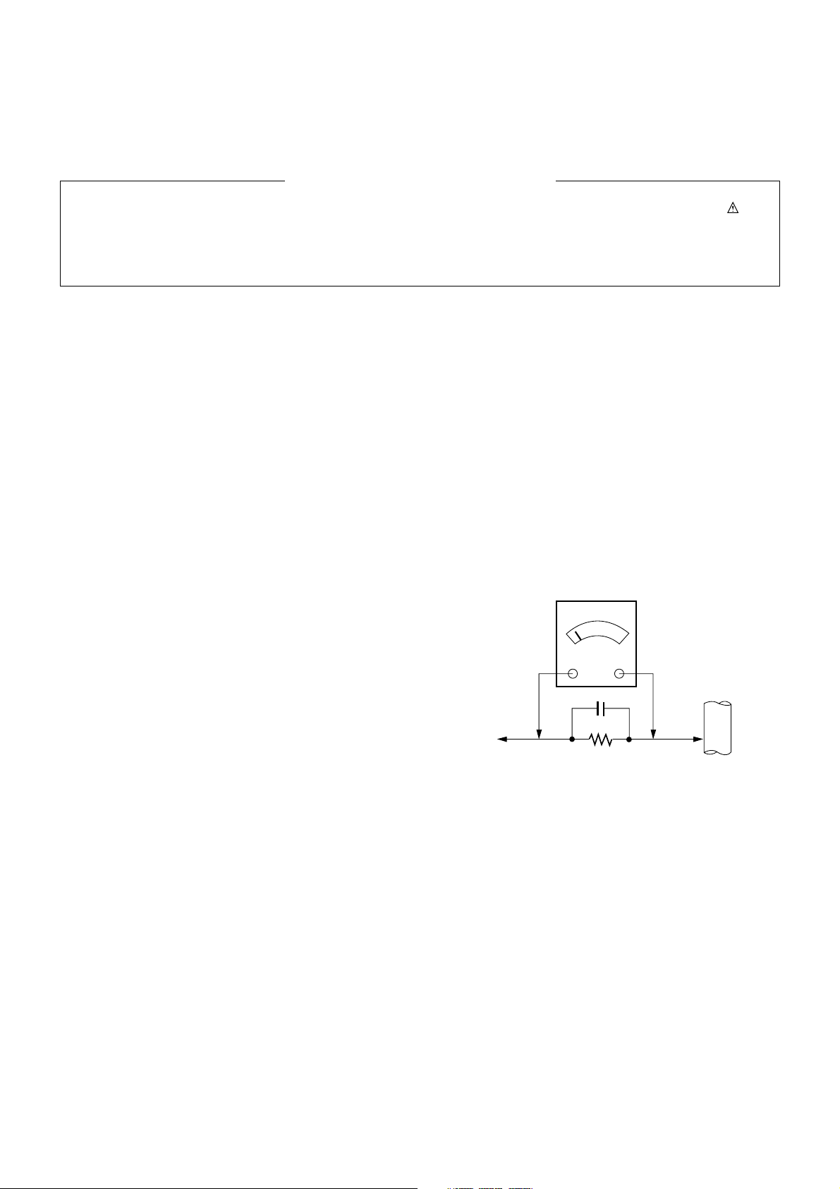
Leakage Current Hot Check (See below Figure)
Plug the AC cord directly into the AC outlet.
Do not use a line Isolation Transformer during this check.
Connect 1.5K/10watt resistor in parallel with a 0.15uF capacitor
between a known good earth ground (Water Pipe, Conduit, etc.)
and the exposed metallic parts.
Measure the AC voltage across the resistor using AC voltmeter
with 1000 ohms/volt or more sensitivity.
Reverse plug the AC cord into the AC outlet and repeat AC voltage
measurements for each exposed metallic part. Any voltage
measured must not exceed 0.75 volt RMS which is corresponds to
0.5mA.
In case any measurement is out of the limits specified, there is
possibility of shock hazard and the set must be checked and
repaired before it is returned to the customer.
Leakage Current Hot Check circuit
1.5 Kohm/10W
To Instrument's
exposed
METALLIC PARTS
Good Earth Ground
such as WATER PIPE,
CONDUIT etc.
AC Volt-meter
IMPORTANT SAFETY NOTICE
0.15uF

LGE Internal Use OnlyCopyright © 2007 LG Electronics. Inc. All right reserved.
Only for training and service purposes
- 4 -
CAUTION: Before servicing receivers covered by this service
manual and its supplements and addenda, read and follow the
SAFETY PRECAUTIONS on page 3 of this publication.
NOTE: If unforeseen circumstances create conflict between the
following servicing precautions and any of the safety precautions on
page 3 of this publication, always follow the safety precautions.
Remember: Safety First.
General Servicing Precautions
1. Always unplug the receiver AC power cord from the AC power
source before;
a. Removing or reinstalling any component, circuit board
module or any other receiver assembly.
b. Disconnecting or reconnecting any receiver electrical plug or
other electrical connection.
c. Connecting a test substitute in parallel with an electrolytic
capacitor in the receiver.
CAUTION: A wrong part substitution or incorrect polarity
installation of electrolytic capacitors may result in an
explosion hazard.
2. Test high voltage only by measuring it with an appropriate high
voltage meter or other voltage measuring device (DVM,
FETVOM, etc) equipped with a suitable high voltage probe.
Do not test high voltage by "drawing an arc".
3. Do not spray chemicals on or near this receiver or any of its
assemblies.
4. Unless specified otherwise in this service manual, clean
electrical contacts only by applying the following mixture to the
contacts with a pipe cleaner, cotton-tipped stick or comparable
non-abrasive applicator; 10% (by volume) Acetone and 90% (by
volume) isopropyl alcohol (90%-99% strength)
CAUTION: This is a flammable mixture.
Unless specified otherwise in this service manual, lubrication of
contacts in not required.
5. Do not defeat any plug/socket B+ voltage interlocks with which
receivers covered by this service manual might be equipped.
6. Do not apply AC power to this instrument and/or any of its
electrical assemblies unless all solid-state device heat sinks are
correctly installed.
7. Always connect the test receiver ground lead to the receiver
chassis ground before connecting the test receiver positive
lead.
Always remove the test receiver ground lead last.
8. Use with this receiver only the test fixtures specified in this
service manual.
CAUTION: Do not connect the test fixture ground strap to any
heat sink in this receiver.
Electrostatically Sensitive (ES) Devices
Some semiconductor (solid-state) devices can be damaged easily
by static electricity. Such components commonly are called
Electrostatically Sensitive (ES) Devices. Examples of typical ES
devices are integrated circuits and some field-effect transistors and
semiconductor "chip" components. The following techniques
should be used to help reduce the incidence of component
damage caused by static by static electricity.
1. Immediately before handling any semiconductor component or
semiconductor-equipped assembly, drain off any electrostatic
charge on your body by touching a known earth ground.
Alternatively, obtain and wear a commercially available
discharging wrist strap device, which should be removed to
prevent potential shock reasons prior to applying power to the
unit under test.
2. After removing an electrical assembly equipped with ES
devices, place the assembly on a conductive surface such as
aluminum foil, to prevent electrostatic charge buildup or
exposure of the assembly.
3. Use only a grounded-tip soldering iron to solder or unsolder ES
devices.
4. Use only an anti-static type solder removal device. Some solder
removal devices not classified as "anti-static" can generate
electrical charges sufficient to damage ES devices.
5. Do not use freon-propelled chemicals. These can generate
electrical charges sufficient to damage ES devices.
6. Do not remove a replacement ES device from its protective
package until immediately before you are ready to install it.
(Most replacement ES devices are packaged with leads
electrically shorted together by conductive foam, aluminum foil
or comparable conductive material).
7. Immediately before removing the protective material from the
leads of a replacement ES device, touch the protective material
to the chassis or circuit assembly into which the device will be
installed.
CAUTION: Be sure no power is applied to the chassis or circuit,
and observe all other safety precautions.
8. Minimize bodily motions when handling unpackaged
replacement ES devices. (Otherwise harmless motion such as
the brushing together of your clothes fabric or the lifting of your
foot from a carpeted floor can generate static electricity
sufficient to damage an ES device.)
General Soldering Guidelines
1. Use a grounded-tip, low-wattage soldering iron and appropriate
tip size and shape that will maintain tip temperature within the
range or 500
°F to 600°F.
2. Use an appropriate gauge of RMA resin-core solder composed
of 60 parts tin/40 parts lead.
3. Keep the soldering iron tip clean and well tinned.
4. Thoroughly clean the surfaces to be soldered. Use a mall wirebristle (0.5 inch, or 1.25cm) brush with a metal handle.
Do not use freon-propelled spray-on cleaners.
5. Use the following unsoldering technique
a. Allow the soldering iron tip to reach normal temperature.
(500
°F to 600°F)
b. Heat the component lead until the solder melts.
c. Quickly draw the melted solder with an anti-static, suction-
type solder removal device or with solder braid.
CAUTION: Work quickly to avoid overheating the circuit
board printed foil.
6. Use the following soldering technique.
a. Allow the soldering iron tip to reach a normal temperature
(500
°F to 600°F)
b. First, hold the soldering iron tip and solder the strand against
the component lead until the solder melts.
c. Quickly move the soldering iron tip to the junction of the
component lead and the printed circuit foil, and hold it there
only until the solder flows onto and around both the
component lead and the foil.
CAUTION: Work quickly to avoid overheating the circuit
board printed foil.
d. Closely inspect the solder area and remove any excess or
splashed solder with a small wire-bristle brush.
SERVICING PRECAUTIONS

LGE Internal Use OnlyCopyright © 2007 LG Electronics. Inc. All right reserved.
Only for training and service purposes
- 5 -
IC Remove/Replacement
Some chassis circuit boards have slotted holes (oblong) through
which the IC leads are inserted and then bent flat against the
circuit foil. When holes are the slotted type, the following technique
should be used to remove and replace the IC. When working with
boards using the familiar round hole, use the standard technique
as outlined in paragraphs 5 and 6 above.
Removal
1. Desolder and straighten each IC lead in one operation by gently
prying up on the lead with the soldering iron tip as the solder
melts.
2. Draw away the melted solder with an anti-static suction-type
solder removal device (or with solder braid) before removing the
IC.
Replacement
1. Carefully insert the replacement IC in the circuit board.
2. Carefully bend each IC lead against the circuit foil pad and
solder it.
3. Clean the soldered areas with a small wire-bristle brush.
(It is not necessary to reapply acrylic coating to the areas).
"Small-Signal" Discrete Transistor
Removal/Replacement
1. Remove the defective transistor by clipping its leads as close as
possible to the component body.
2. Bend into a "U" shape the end of each of three leads remaining
on the circuit board.
3. Bend into a "U" shape the replacement transistor leads.
4. Connect the replacement transistor leads to the corresponding
leads extending from the circuit board and crimp the "U" with
long nose pliers to insure metal to metal contact then solder
each connection.
Power Output, Transistor Device
Removal/Replacement
1. Heat and remove all solder from around the transistor leads.
2. Remove the heat sink mounting screw (if so equipped).
3. Carefully remove the transistor from the heat sink of the circuit
board.
4. Insert new transistor in the circuit board.
5. Solder each transistor lead, and clip off excess lead.
6. Replace heat sink.
Diode Removal/Replacement
1. Remove defective diode by clipping its leads as close as
possible to diode body.
2. Bend the two remaining leads perpendicular y to the circuit
board.
3. Observing diode polarity, wrap each lead of the new diode
around the corresponding lead on the circuit board.
4. Securely crimp each connection and solder it.
5. Inspect (on the circuit board copper side) the solder joints of
the two "original" leads. If they are not shiny, reheat them and if
necessary, apply additional solder.
Fuse and Conventional Resistor
Removal/Replacement
1. Clip each fuse or resistor lead at top of the circuit board hollow
stake.
2. Securely crimp the leads of replacement component around
notch at stake top.
3. Solder the connections.
CAUTION: Maintain original spacing between the replaced
component and adjacent components and the circuit board to
prevent excessive component temperatures.
Circuit Board Foil Repair
Excessive heat applied to the copper foil of any printed circuit
board will weaken the adhesive that bonds the foil to the circuit
board causing the foil to separate from or "lift-off" the board. The
following guidelines and procedures should be followed whenever
this condition is encountered.
At IC Connections
To repair a defective copper pattern at IC connections use the
following procedure to install a jumper wire on the copper pattern
side of the circuit board. (Use this technique only on IC
connections).
1. Carefully remove the damaged copper pattern with a sharp
knife. (Remove only as much copper as absolutely necessary).
2. carefully scratch away the solder resist and acrylic coating (if
used) from the end of the remaining copper pattern.
3. Bend a small "U" in one end of a small gauge jumper wire and
carefully crimp it around the IC pin. Solder the IC connection.
4. Route the jumper wire along the path of the out-away copper
pattern and let it overlap the previously scraped end of the good
copper pattern. Solder the overlapped area and clip off any
excess jumper wire.
At Other Connections
Use the following technique to repair the defective copper pattern
at connections other than IC Pins. This technique involves the
installation of a jumper wire on the component side of the circuit
board.
1. Remove the defective copper pattern with a sharp knife.
Remove at least 1/4 inch of copper, to ensure that a hazardous
condition will not exist if the jumper wire opens.
2. Trace along the copper pattern from both sides of the pattern
break and locate the nearest component that is directly
connected to the affected copper pattern.
3. Connect insulated 20-gauge jumper wire from the lead of the
nearest component on one side of the pattern break to the lead
of the nearest component on the other side.
Carefully crimp and solder the connections.
CAUTION: Be sure the insulated jumper wire is dressed so the
it does not touch components or sharp edges.
LGE Internal Use OnlyCopyright © 2007 LG Electronics. Inc. All right reserved.
Only for training and service purposes
- 6 -
SPECIFICATION
NOTE : Specifications and others are subject to change without notice for improvement
.
1. General Specification(LCD MODULE)
2. Model General Specification
Item Specification Remark
Market UK, France, Germany, Spain, Sweden, Finland, Italy
Broadcasting system PAL-BG UK, France, Germany, Spain, Sweden, Finland, Italy
PAL-DK
PAL-I,I’
DVB-T (ID TV)
Receiving system Analog : Upper Heterodyne
Digital : COFDM
Scart Jack (2EA) PAL, SECAM Scart 1 Jack is Full scart and support RF-OUT(analog)
Scart 2 jack is Half scart and support MNT-OUT.
Video Input (2EA) PAL, SECAM, NTSC 4 System :
PAL, SECAM, NTSC, PAL60
S-Video Input (1EA) PAL, SECAM, NTSC 4 System :
PAL, SECAM, NTSC, PAL60
Component Input (1EA) Y/Cb/Cr, Y/ Pb/Pr
RGB Input RGB-PC,
RGB-DTV
HDMI Input (2EA) HDMI-PC
HDMI-DTV & SOUND
Audio Input (4 EA) PC Audio, Component, AV (2EA) L/R Input
Item Specification Remark
Display Screen Device 32” wide Color Display Module LCD
Aspect Ratio 16:9
LCD Module 32” TFT WXGA LCD MAKER : LPL
Operating Environment Temp. : 0 ~ 40 deg
Humidity : 0 ~ 85% LGE SPEC
Storage Environment Temp. : -20 ~ 60 deg
Humidity : 0 ~ 85 %
Input Voltage 100-240V~, 50/60Hz
Power Consumption Power on (Green)
Total 114.32W (Typ.) (Logic=4.32(4.1)W, Backlight =110W )
St-By (Red) : 1.0 W
Type Size 760.0 x 450.0 x 48.0
Pixel Pitch 0.17025 x 0.51075
Back Light 18 EEFL
Display Colors 16.7M (16,777,216)
Coating 3H, AG
LGE Internal Use OnlyCopyright © 2007 LG Electronics. Inc. All right reserved.
Only for training and service purposes
Item Min Typ Max Unit Maker Remark
Luminance 400 500 cd/m LPL(0RT)32” -50cm from the surface
(W/O PC mode) - Full White Pattern
View angle (R/L, U/D) 178/178 degree 32”
Color Coordinate White X Typ. 0.279/0.279/0.279 Typ. LPL 32”
Y -0.03 0.292/0.292/0.292 +0.03
Red X 0.635/0.636/0.635
Y 0.339/0.343/0.344
Green X 0.282/0.284/0.286
Y 0.606/0.615/0.614
Blue X 0.145/0.144/0.146
Y 0.064/0.063/0.061
Contrast ratio
(W/O PC mode) 600 800 32” LPL(0-RT)
Luminance Variation 1.3
- 7 -
3. Chroma & Brightness (LCD Module-LPL)
4. Component Video Input (Y, PB, PR)
No
Specification
Proposed
Resolution H-freq(kHz) V-freq(Hz)
1 720*480 15.73 60.00 SDTV, DVD 480i
2 720*480 15.63 59.94 SDTV, DVD 480i
3 720*480 31.47 59.94 480p
4 720*576 15.625 50.00 SDTV, DVD 625 Line
5 720*576 31.25 50.00 HDTV 576p
6 1280*720 45.00 50.00 HDTV 720p
7 1280*720 44.96 59.94 HDTV 720p
8 1920*1080 31.25 50.00 HDTV 1080i
9 1920*1080 33.75 60.00 HDTV 1080i
10 1920*1080 33.72 59.94 HDTV 1080i
LGE Internal Use OnlyCopyright © 2007 LG Electronics. Inc. All right reserved.
Only for training and service purposes
- 8 -
6. HDMI input (DTV Mode)
5. RGB PC INPUT Mode Table
No Resolution H-freq(kHz) V-freq.(Hz) Pixel clock(MHz) Proposed Remark
1. 720*400 31.468 70.08 28.321
2. 640*480 31.469 59.94 25.17 VESA Input 848*480 60Hz, 852*480 60Hz
37.684 75.00 31.50 --> 640*480 60Hz Display
3 800*600 37.879 60.31 40.00 VESA
46.875 75.00 49.50
4 832*624 49.725 74.55 57.283 Macintosh
5 1024*768 48.363 60.00 65.00 VESA(XGA)
56.470 70.00 75.00
60.123 75.029 78.75
6 1280*768 47.78 59.87 79.5 WXGA
7 1360*768 47.72 59.8 84.75 WXGA
8 1366*768 47.56 59.6 84.75 WXGA
9 1280*1024 63.595 60.0 108.875 SXGA FHD Model only
10 1400*1050 65.160 60.0 122.50 SXGA FHD Model only
11 1600*1200 74.077 60.0 130.375 UXGA Reduced Blanking Timing, FHD Model only
Input 1920*1200 60Hz -> 1600*1200 60Hz Display
12 1920*1080 66.647 59.988 138.625 WUXGA Reduced Blanking Timing
No Resolution H-freq(kHz) V-freq.(Hz) Pixel clock(MHz) Proposed Remark
1. 720*480 31.47 59.94 27.00 SDTV 480P(4:3) PC mode -> 640*480 60Hz Display
2. 720*480 31.50 60 27.027 SDTV 480P(4:3)
3. 640*480 31.469 59.94 25.175 SDTV 480P(4:3)
4. 640*480 31.469 60.00 25.20 SDTV 480P(4:3)
5. 720*480 31.47 59.94 27.000 SDTV 480P(16:9)
6. 720*480 31.50 60.00 27.027 SDTV 480P(16:9)
7. 720*576 31.25 50.00 27.000 SDTV 576P
8. 1280*720 37.50 50.00 74.176 HDTV 720P
9. 1280*720 44.96 59.94 74.176 HDTV 720P PC mode -> 1280*720 60Hz Display
10. 1280*720 45.00 60.00 74.250 HDTV 720P
11 1920*1080 33.72 59.94 74.176 HDTV 1080I
12 1920*1080 33.75 60.00 74.250 HDTV 1080I
13 1920*1080 28.125 50.00 74.250 HDTV 1080I 50Hz
14 1920*1080 27.000 24.00 74.250 HDTV 1080P 24Hz
15 1920*1080 56.250 50 148.500 HDTV 1080P 50Hz
16 1920*1080 67.433 59.94 148.352 HDTV 1080P PC mode -> 1920*1080 60Hz Display
17 1920*1080 67.500 60 148.500 HDTV 1080P
LGE Internal Use OnlyCopyright © 2007 LG Electronics. Inc. All right reserved.
Only for training and service purposes
- 9 -
7. HDMI input (PC Mode)
No Resolution H-freq(kHz) V-freq.(Hz) Pixel clock(MHz) Proposed Remark
1. 720*400 31.468 70.08 28.321
2. 640*480 31.469 59.94 25.17 VESA DTV mode --> 480p Display
37.684 75.00 31.50 848*480 60Hz, 852*480 60Hz Ë No signal
3 800*600 37.879 60.31 40.00 VESA
46.875 75.00 49.50
4. 832*624 49.725 74.55 57.283 Macintosh
5. 1024*768 48.363 60.00 65.00 VESA(XGA)
56.470 70.00 75.00
60.123 75.029 78.75
6 1280*768 47.78 59.87 79.5 WXGA PC mode only
7 1360*768 47.72 59.8 84.75 WXGA
8 1366*768 47.56 59.6 84.75 WXGA
9 1280*1024 63.595 60.0 108.875 SXGA FHD Model only
10 1400*1050 65.160 60.0 122.50 SXGA FHD Model only
11 1600*1200 74.077 60.0 130.375 UXGA Reduced Blanking Timing, FHD Model only
Input 1920*1200 60Hz --> No Signal
12 1920*1080 66.647 59.988 138.625 WUXGA Reduced Blanking Timing
DTV mode --> 1080P Display
LGE Internal Use OnlyCopyright © 2007 LG Electronics. Inc. All right reserved.
Only for training and service purposes
- 10 -
ADJUSTMENT INSTRUCTION
1. Application Range
This spec. sheet is applied to all of the LD74A chassis
manufactured at LG TV Plant all over the world.
2. Specification.
1) Because this is not a hot chassis, it is not necessary to use
an isolation transformer.
However, the use of isolation transformer will help to
protect test instruments
2) Adjustment must be done in the correct sequence.
3) The adjustment must be performed at 25±5°C temperature
and 65±10% relative humidity if there is no specified
designation.
4) The input voltage of the receiver must be kept between
100-220V~, 50/60Hz.
5) Before adjustment, execute Heat-Run for 30 minutes at RF
no signal.
3. Channel Memory
1) Press ADJ key in Adjust remote control.
2) Select “Channel Recover” by using
D/E (CH+/-) key, and
press
G (VOL+).
3) The set is turned off automatically.
4) Press ‘power’ key of Adjust Remote control.
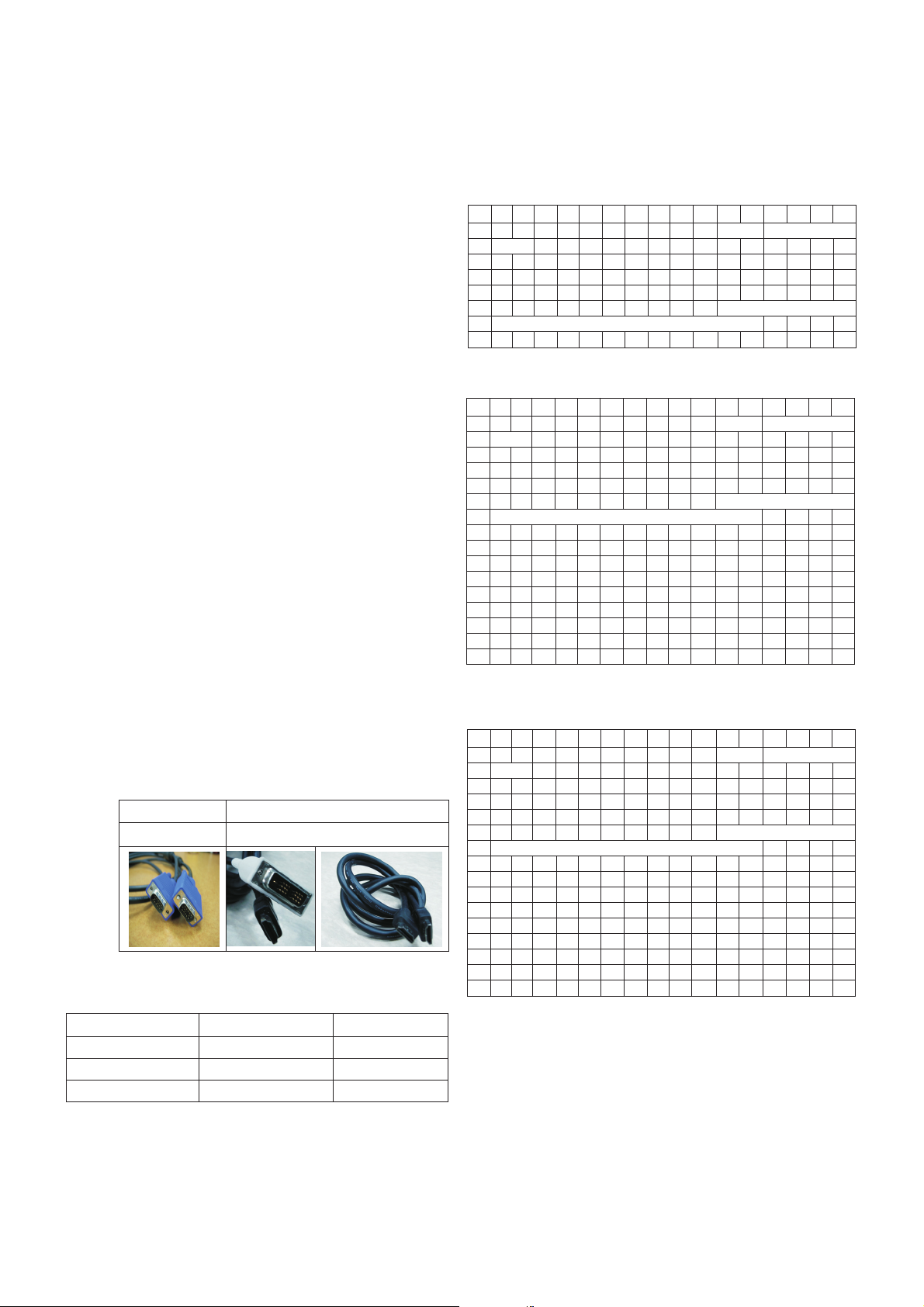
4. EDID
* Caution
1) Use the proper signal cable for EDID Download
- Analog EDID : Pin3 exists
- Digital EDID : Pin3 exists
2) Never connect HDMI & D-sub Cable at the same time.
3) Use the proper cables below for EDID Writing.
4) Download HDMI1, HDMI2 separately because HDMI1 is
different from HDMI2.
4.1. EDID Data
4.2. Data
(1) ANALOG (128 bytes)
(2) HDMI 1 (256 bytes)=>
=> Detail EDID Options are below (a, b, c, d, e-1, e-2, f-1, f-2)
(3) HDMI 2 (256 bytes)
=> Detail EDID Options are below (a, b, c, d, e-1, e-2, f-1, f-2)
ⓐ Product ID
ⓑ Serial No: Controlled on production line.
ⓒ Month, Year: Controlled on production line:
ex) Monthly : ‘09’ -> ‘09’
Year : ‘2006’ -> ‘10’
ⓓ Model Name(Hex):
ⓔ-1, ⓔ-2, ⓕ-1, ⓕ-2 Checksum: Changeable by total
EDID data.
Item
Manufacurer ID
Version
Revision
Condition
GSM
Digital : 1
Digital : 3
Data(Hex)
1E6D
01
03
D-sub to D-sub DVI-D to HDMI or HDMI ro HDMI
For HDMI EDID
0x000x01 0x02 0x03 0x04 0x05 0x06 0x07 0x08 0x09 0x0A 0x0B0x0C 0x0D 0x0E0x0F
0x00 00 FF FF FF FF FF FF 00 1E 6D ⓐⓑ
0x01 ⓒ 01 03 01 46 27 78 EA D9 B0 A3 57 49 9C 25
0x02 11 49 4B A5 6E 00 31 40 45 40 61 40 D1 C0 01 01
0x03 01 01 01 01 01 01 1B 21 50 A0 51 00 1E 30 48 88
0x04 35 00 BC 86 21 00 00 1C 26 36 80 A0 70 38 1F 40
0x05 50 20 85 04 BC 86 21 00 00 18 ⓓ
0x06 ⓓ 00 00 00 FD
0x07 00 3C 4B 1D 43 0E 00 0A 20 20 20 20 20 20 00 ⓔ-1
For Analog EDID
0x000x01 0x02 0x03 0x04 0x05 0x06 0x07 0x08 0x09 0x0A 0x0B0x0C 0x0D 0x0E0x0F
0x00 00 FF FF FF FF FF FF 00 1E 6D ⓐⓑ
0x01 ⓒ 01 03 80 46 27 78 EA D9 B0 A3 57 49 9C 25
0x02 11 49 4B A5 6E 00 31 40 45 40 61 40 D1 C0 01 01
0x03 01 01 01 01 01 01 02 3A 80 18 71 38 2D 40 58 2C
0x04 45 00 C4 8E 21 00 00 1E 1B 21 50 A0 51 00 1E 30
0x05 48 88 35 00 BC 86 21 00 00 1C ⓓ
0x06 ⓓ 00 00 00 FD
0x07 00 32 4B 1C 43 0F 00 0A 20 20 20 20 20 20 01 ⓔ-2
0x00 02 03 21 F1 4E 02 11 01 03 12 13 04 14 05 21 1F
0x01 20 22 10 23 09 07 07 83 01 00 00 65 3 0C 00 10
0x02 00 01 1D 00 BC 52 D0 1E 20 B8 28 55 40 C4 8E 21
0x03 00 00 1E 01 1D 00 72 51 D0 1E 20 6E 28 55 00 C4
0x04 8E 21 00 00 1E 01 1D 80 D0 72 1C 16 20 10 2C 25
0x05 80 C4 8E 21 00 00 9E 8C 0A D0 90 20 40 31 20 0C
0x06 40 55 00 C4 8E 21 00 00 18 4E 1F 00 80 51 00 1E
0x07 30 40 80 37 00 BC 88 21 00 00 18 00 00 00 00 ⓕ-1
0x000x01 0x02 0x03 0x04 0x05 0x06 0x07 0x08 0x09 0x0A 0x0B0x0C 0x0D 0x0E0x0F
0x00 0 FF FF FF FF FF FF 0 1E 6D ⓐⓑ
0x01 ⓒ 1 3 80 46 27 78 EA D9 B0 A3 57 49 9C 25
0x02 11 49 4B A5 6E 0 31 40 45 40 61 40 D1 C0 1 1
0x03 1 1 1 1 1 1 2 3A 80 18 71 38 2D 40 58 2C
0x04 45 0 C4 8E 21 0 0 1E 1B 21 50 A0 51 0 1E 30
0x05 48 88 35 0 BC 86 21 0 0 1C ⓓ
0x06 ⓓ 000FD
0x07 0 32 4B 1C 43 0F 0 0A 20 20 20 20 20 20 1 ⓔ-2
0x00 2 3 21 F1 4E 2 11 1 3 12 13 4 14 5 21 1F
0x01 20 22 10 23 9 7 7 83 1 0 0 65 3 0C 0 10
0x02 0 1 1D 0 BC 52 D0 1E 20 B8 28 55 40 C4 8E 21
0x03 0 0 1E 1 1D 0 72 51 D0 1E 20 6E 28 55 0 C4
0x04 8E 21 0 0 1E 1 1D 80 D0 72 1C 16 20 10 2C 25
0x05 80 C4 8E 21 0 0 9E 8C 0A D0 90 20 40 31 20 0C
0x06 40 55 0 C4 8E 21 0 0 18 4E 1F 0 80 51 0 1E
0x07 30 40 80 37 0 BC 88 21 0 0 18 0 0 0 0 ⓕ-2
 Loading...