

LG 32LD310H, 32LD310H-UA, 32LD320H, 32LD320H-UA Service Manual
LCD TV
SERVICE MANUAL
CAUTION
BEFORE SERVICING THE CHASSIS,
READ THE SAFETY PRECAUTIONS IN THIS MANUAL.
CHASSIS : LA06A
MODEL : 32LD310H
32LD310H-UA
32LD320H 32LD320H-UA
North/Latin America http://aic.lgservice.com
Europe/Africa http://eic.lgservice.com
Asia/Oceania http://biz.lgservice.com
Internal Use Only
Printed in KoreaP/NO : MFL66280202 (1101-REV01)

LGE Internal Use OnlyCopyright LG Electronics. Inc. All right reserved.
Only for training and service purposes
- 2 -
CONTENTS
CONTENTS .............................................................................................. 2
SAFETY PRECAUTIONS ......................................................................... 3
SPECIFICATION....................................................................................... 6
ADJUSTMENT INSTRUCTION .............................................................. 10
EXPLODED VIEW .................................................................................. 19
SVC. SHEET ...............................................................................................
LGE Internal Use OnlyCopyright LG Electronics. Inc. All right reserved.
Only for training and service purposes
- 3 -
SAFETY PRECAUTIONS
Many electrical and mechanical parts in this chassis have special safety-related characteristics. These parts are identified by in the
Schematic Diagram and Exploded View.
It is essential that these special safety parts should be replaced with the same components as recommended in this manual to prevent
Shock, Fire, or other Hazards.
Do not modify the original design without permission of manufacturer.
General Guidance
An isolation Transformer should always be used during the
servicing of a receiver whose chassis is not isolated from the AC
power line. Use a transformer of adequate power rating as this
protects the technician from accidents resulting in personal injury
from electrical shocks.
It will also protect the receiver and it's components from being
damaged by accidental shorts of the circuitry that may be
inadvertently introduced during the service operation.
If any fuse (or Fusible Resistor) in this TV receiver is blown,
replace it with the specified.
When replacing a high wattage resistor (Oxide Metal Film Resistor,
over 1W), keep the resistor 10mm away from PCB.
Keep wires away from high voltage or high temperature parts.
Before returning the receiver to the customer,
always perform an AC leakage current check on the exposed
metallic parts of the cabinet, such as antennas, terminals, etc., to
be sure the set is safe to operate without damage of electrical
shock.
Leakage Current Cold Check(Antenna Cold Check)
With the instrument AC plug removed from AC source, connect an
electrical jumper across the two AC plug prongs. Place the AC
switch in the on position, connect one lead of ohm-meter to the AC
plug prongs tied together and touch other ohm-meter lead in turn to
each exposed metallic parts such as antenna terminals, phone
jacks, etc.
If the exposed metallic part has a return path to the chassis, the
measured resistance should be between 1MΩ and 5.2MΩ.
When the exposed metal has no return path to the chassis the
reading must be infinite.
An other abnormality exists that must be corrected before the
receiver is returned to the customer.
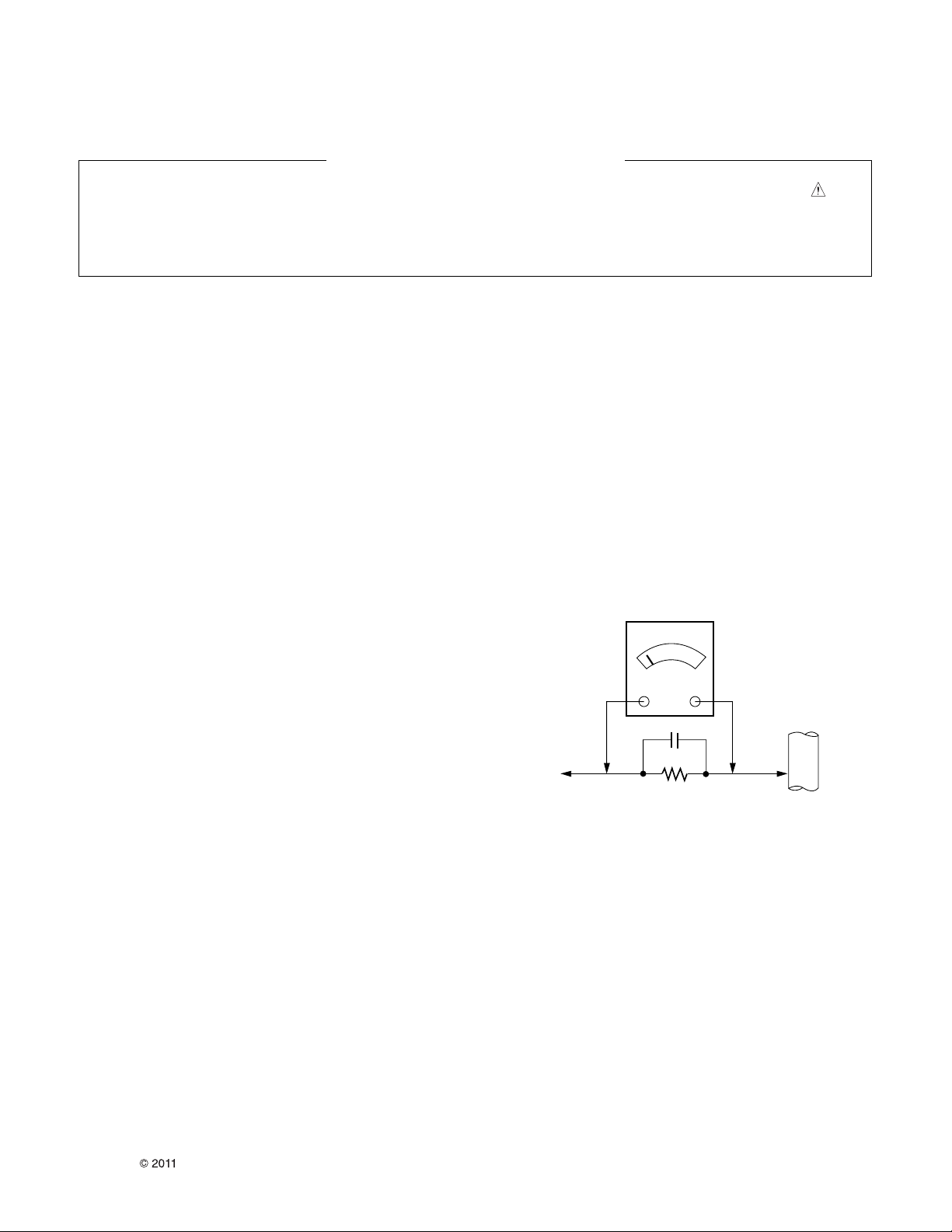
Leakage Current Hot Check (See below Figure)
Plug the AC cord directly into the AC outlet.
Do not use a line Isolation Transformer during this check.
Connect 1.5K/10watt resistor in parallel with a 0.15uF capacitor
between a known good earth ground (Water Pipe, Conduit, etc.)
and the exposed metallic parts.
Measure the AC voltage across the resistor using AC voltmeter
with 1000 ohms/volt or more sensitivity.
Reverse plug the AC cord into the AC outlet and repeat AC voltage
measurements for each exposed metallic part. Any voltage
measured must not exceed 0.75 volt RMS which is corresponds to
0.5mA.
In case any measurement is out of the limits specified, there is
possibility of shock hazard and the set must be checked and
repaired before it is returned to the customer.
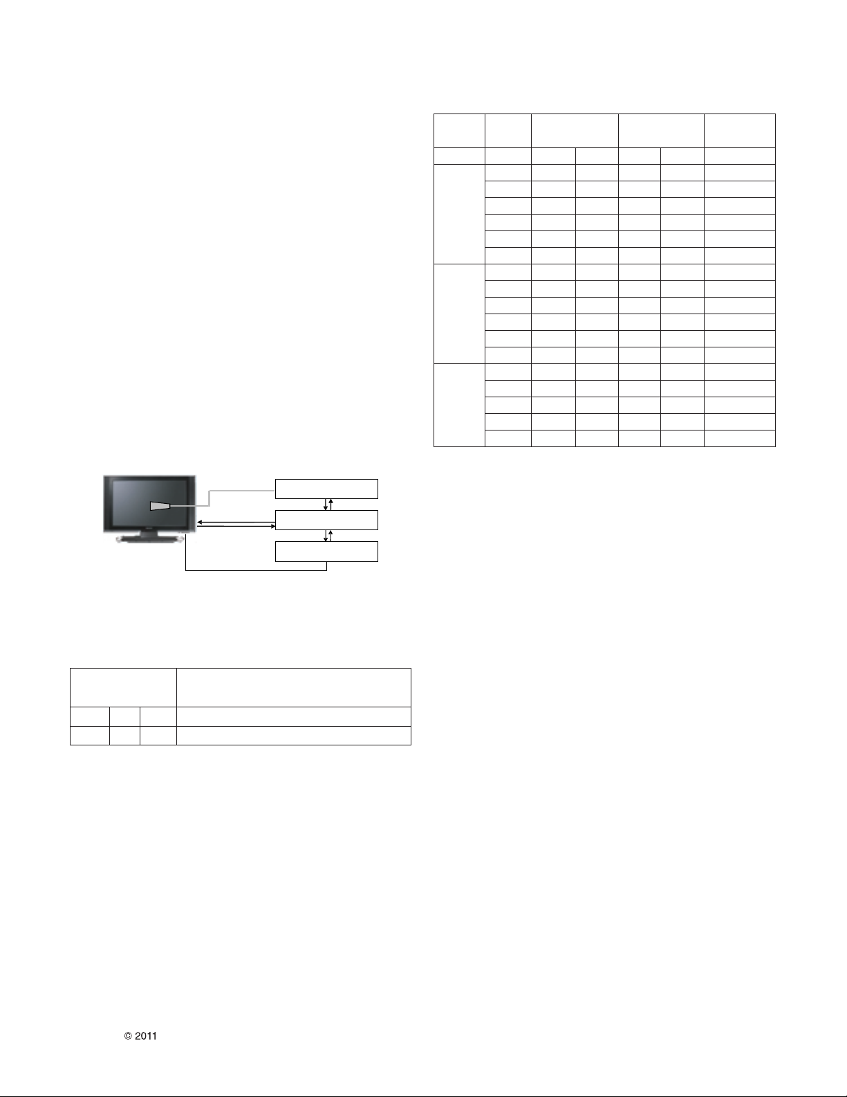
Leakage Current Hot Check circuit
1.5 Kohm/10W
To Instrument's
exposed
METALLIC PARTS
Good Earth Ground
such as WATER PIPE,
CONDUIT etc.
AC Volt-meter
IMPORTANT SAFETY NOTICE
0.15uF

LGE Internal Use OnlyCopyright LG Electronics. Inc. All right reserved.
Only for training and service purposes
- 4 -
CAUTION: Before servicing receivers covered by this service
manual and its supplements and addenda, read and follow the
SAFETY PRECAUTIONS on page 3 of this publication.
NOTE: If unforeseen circumstances create conflict between the
following servicing precautions and any of the safety precautions on
page 3 of this publication, always follow the safety precautions.
Remember: Safety First.
General Servicing Precautions
1. Always unplug the receiver AC power cord from the AC power
source before;
a. Removing or reinstalling any component, circuit board
module or any other receiver assembly.
b. Disconnecting or reconnecting any receiver electrical plug or
other electrical connection.
c. Connecting a test substitute in parallel with an electrolytic
capacitor in the receiver.
CAUTION: A wrong part substitution or incorrect polarity
installation of electrolytic capacitors may result in an
explosion hazard.
2. Test high voltage only by measuring it with an appropriate high
voltage meter or other voltage measuring device (DVM,
FETVOM, etc) equipped with a suitable high voltage probe.
Do not test high voltage by "drawing an arc".
3. Do not spray chemicals on or near this receiver or any of its
assemblies.
4. Unless specified otherwise in this service manual, clean
electrical contacts only by applying the following mixture to the
contacts with a pipe cleaner, cotton-tipped stick or comparable
non-abrasive applicator; 10% (by volume) Acetone and 90% (by
volume) isopropyl alcohol (90%-99% strength)
CAUTION: This is a flammable mixture.
Unless specified otherwise in this service manual, lubrication of
contacts in not required.
5. Do not defeat any plug/socket B+ voltage interlocks with which
receivers covered by this service manual might be equipped.
6. Do not apply AC power to this instrument and/or any of its
electrical assemblies unless all solid-state device heat sinks are
correctly installed.
7. Always connect the test receiver ground lead to the receiver
chassis ground before connecting the test receiver positive
lead.
Always remove the test receiver ground lead last.
8. Use with this receiver only the test fixtures specified in this
service manual.
CAUTION: Do not connect the test fixture ground strap to any
heat sink in this receiver.
Electrostatically Sensitive (ES) Devices
Some semiconductor (solid-state) devices can be damaged easily
by static electricity. Such components commonly are called
Electrostatically Sensitive (ES) Devices. Examples of typical ES
devices are integrated circuits and some field-effect transistors and
semiconductor "chip" components. The following techniques
should be used to help reduce the incidence of component
damage caused by static by static electricity.
1. Immediately before handling any semiconductor component or
semiconductor-equipped assembly, drain off any electrostatic
charge on your body by touching a known earth ground.
Alternatively, obtain and wear a commercially available
discharging wrist strap device, which should be removed to
prevent potential shock reasons prior to applying power to the
unit under test.
2. After removing an electrical assembly equipped with ES
devices, place the assembly on a conductive surface such as
aluminum foil, to prevent electrostatic charge buildup or
exposure of the assembly.
3. Use only a grounded-tip soldering iron to solder or unsolder ES
devices.
4. Use only an anti-static type solder removal device. Some solder
removal devices not classified as "anti-static" can generate
electrical charges sufficient to damage ES devices.
5. Do not use freon-propelled chemicals. These can generate
electrical charges sufficient to damage ES devices.
6. Do not remove a replacement ES device from its protective
package until immediately before you are ready to install it.
(Most replacement ES devices are packaged with leads
electrically shorted together by conductive foam, aluminum foil
or comparable conductive material).
7. Immediately before removing the protective material from the
leads of a replacement ES device, touch the protective material
to the chassis or circuit assembly into which the device will be
installed.
CAUTION: Be sure no power is applied to the chassis or circuit,
and observe all other safety precautions.
8. Minimize bodily motions when handling unpackaged
replacement ES devices. (Otherwise harmless motion such as
the brushing together of your clothes fabric or the lifting of your
foot from a carpeted floor can generate static electricity
sufficient to damage an ES device.)
General Soldering Guidelines
1. Use a grounded-tip, low-wattage soldering iron and appropriate
tip size and shape that will maintain tip temperature within the
range or 500°F to 600°F.
2. Use an appropriate gauge of RMA resin-core solder composed
of 60 parts tin/40 parts lead.
3. Keep the soldering iron tip clean and well tinned.
4. Thoroughly clean the surfaces to be soldered. Use a mall wirebristle (0.5 inch, or 1.25cm) brush with a metal handle.
Do not use freon-propelled spray-on cleaners.
5. Use the following unsoldering technique
a. Allow the soldering iron tip to reach normal temperature.
(500°F to 600°F)
b. Heat the component lead until the solder melts.
c. Quickly draw the melted solder with an anti-static, suction-
type solder removal device or with solder braid.
CAUTION: Work quickly to avoid overheating the circuit
board printed foil.
6. Use the following soldering technique.
a. Allow the soldering iron tip to reach a normal temperature
(500°F to 600°F)
b. First, hold the soldering iron tip and solder the strand against
the component lead until the solder melts.
c. Quickly move the soldering iron tip to the junction of the
component lead and the printed circuit foil, and hold it there
only until the solder flows onto and around both the
component lead and the foil.
CAUTION: Work quickly to avoid overheating the circuit
board printed foil.
d. Closely inspect the solder area and remove any excess or
splashed solder with a small wire-bristle brush.
SERVICING PRECAUTIONS

LGE Internal Use OnlyCopyright LG Electronics. Inc. All right reserved.
Only for training and service purposes
- 5 -
IC Remove/Replacement
Some chassis circuit boards have slotted holes (oblong) through
which the IC leads are inserted and then bent flat against the
circuit foil. When holes are the slotted type, the following technique
should be used to remove and replace the IC. When working with
boards using the familiar round hole, use the standard technique
as outlined in paragraphs 5 and 6 above.
Removal
1. Desolder and straighten each IC lead in one operation by gently
prying up on the lead with the soldering iron tip as the solder
melts.
2. Draw away the melted solder with an anti-static suction-type
solder removal device (or with solder braid) before removing the
IC.
Replacement
1. Carefully insert the replacement IC in the circuit board.
2. Carefully bend each IC lead against the circuit foil pad and
solder it.
3. Clean the soldered areas with a small wire-bristle brush.
(It is not necessary to reapply acrylic coating to the areas).
"Small-Signal" Discrete Transistor
Removal/Replacement
1. Remove the defective transistor by clipping its leads as close as
possible to the component body.
2. Bend into a "U" shape the end of each of three leads remaining
on the circuit board.
3. Bend into a "U" shape the replacement transistor leads.
4. Connect the replacement transistor leads to the corresponding
leads extending from the circuit board and crimp the "U" with
long nose pliers to insure metal to metal contact then solder
each connection.
Power Output, Transistor Device
Removal/Replacement
1. Heat and remove all solder from around the transistor leads.
2. Remove the heat sink mounting screw (if so equipped).
3. Carefully remove the transistor from the heat sink of the circuit
board.
4. Insert new transistor in the circuit board.
5. Solder each transistor lead, and clip off excess lead.
6. Replace heat sink.
Diode Removal/Replacement
1. Remove defective diode by clipping its leads as close as
possible to diode body.
2. Bend the two remaining leads perpendicular y to the circuit
board.
3. Observing diode polarity, wrap each lead of the new diode
around the corresponding lead on the circuit board.
4. Securely crimp each connection and solder it.
5. Inspect (on the circuit board copper side) the solder joints of
the two "original" leads. If they are not shiny, reheat them and if
necessary, apply additional solder.
Fuse and Conventional Resistor
Removal/Replacement
1. Clip each fuse or resistor lead at top of the circuit board hollow
stake.
2. Securely crimp the leads of replacement component around
notch at stake top.
3. Solder the connections.
CAUTION: Maintain original spacing between the replaced
component and adjacent components and the circuit board to
prevent excessive component temperatures.
Circuit Board Foil Repair
Excessive heat applied to the copper foil of any printed circuit
board will weaken the adhesive that bonds the foil to the circuit
board causing the foil to separate from or "lift-off" the board. The
following guidelines and procedures should be followed whenever
this condition is encountered.
At IC Connections
To repair a defective copper pattern at IC connections use the
following procedure to install a jumper wire on the copper pattern
side of the circuit board. (Use this technique only on IC
connections).
1. Carefully remove the damaged copper pattern with a sharp
knife. (Remove only as much copper as absolutely necessary).
2. carefully scratch away the solder resist and acrylic coating (if
used) from the end of the remaining copper pattern.
3. Bend a small "U" in one end of a small gauge jumper wire and
carefully crimp it around the IC pin. Solder the IC connection.
4. Route the jumper wire along the path of the out-away copper
pattern and let it overlap the previously scraped end of the good
copper pattern. Solder the overlapped area and clip off any
excess jumper wire.
At Other Connections
Use the following technique to repair the defective copper pattern
at connections other than IC Pins. This technique involves the
installation of a jumper wire on the component side of the circuit
board.
1. Remove the defective copper pattern with a sharp knife.
Remove at least 1/4 inch of copper, to ensure that a hazardous
condition will not exist if the jumper wire opens.
2. Trace along the copper pattern from both sides of the pattern
break and locate the nearest component that is directly
connected to the affected copper pattern.
3. Connect insulated 20-gauge jumper wire from the lead of the
nearest component on one side of the pattern break to the lead
of the nearest component on the other side.
Carefully crimp and solder the connections.
CAUTION: Be sure the insulated jumper wire is dressed so the
it does not touch components or sharp edges.
LGE Internal Use OnlyCopyright LG Electronics. Inc. All right reserved.
Only for training and service purposes
1. Application range
This spec sheet is applied all of the 32”, 37”, 42” LCD TV with
LA06A chassis and 26” LCD TV with LA06B chassis.
2. Requirement for Test
Each part is tested as below without special appointment.
1) Temperature: 25 ºC ± 5 ºC
2) Relative Humidity: 65 ± 10 %
3) Power Voltage : Standard input voltage(100-240V~, 50/60Hz)
* Standard Voltage of each product is marked by models
4) Specification and performance of each parts are followed
each drawing and specification by part number in
accordance with BOM.
5) The receiver must be operated for about 5 minutes prior to
the adjustment.
3. Test method
1) Performance: LGE TV test method followed
2) Demanded other specification
- Safety : UL, CSA, IEC specification
- EMC: FCC, ICES, IEC specification
- 6 -
SPECIFICATION
NOTE : Specifications and others are subject to change without notice for improvement.
4. General Specification(TV)
No Item Specification Remark
1 Receivable System 1) ATSC / NTSC-M
2 Available Channel 1) VHF : 02 ~ 13
2) UHF : 14 ~ 69
3) DTV : 02 ~ 69
4) CATV : 01 ~ 135
5) CADTV : 01 ~ 135
3 Input Voltage 1) AC 100 ~ 120V 50/60Hz Mark : 110V, 60Hz
4 Market North America
5 Screen Size 32 / 37 / 42 inches
6 Aspect Ratio 16:9
7 Tuning System FS
8 LCD Module LC370WUG-SCA1 37LD310H-UA/37LD320H-UA
LC320WXE-SCA1 32LD310H-UA/37LD320H-UA
LC420WUG-SCA1 42LD320H-UA
LC260WXN-SBA3 26LD320H-UA
9 Operating Environment Temp : 0 ~ 40 deg
Humidity : ~ 80 %
10 Storage Environment Temp : -20 ~ 60 deg
Humidity : -85 %
- 7 -
LGE Internal Use OnlyCopyright LG Electronics. Inc. All right reserved.
Only for training and service purposes
5. Chrominance & Luminance
5.1. 32LD310H-UA/32LD320H-UA : LC320WXE-SCA1(LGD)
No. Item Min Typ Max Unit Remarks
1 White brightness 300 350 cd/m
2
EPA 4.0
2 Luminance uniformity 1.25 5point
3 Color coordinate RED X Typ. 0.636 Typ.
(Default) Y -0.03 0.335 +0.03
GREEN X 0.291
Y 0.603
BLUE X 0.146
Y 0.061
WHITE X 0.279
Y 0.292
4 Contrast ratio 800 1200 EPA 4.0, except RGB mode
10,000:1 50,000:1
6 Color Temperature Cool Typ. 0.269 Typ The W/B Tolerance is
-0.015 0.273 +0.015 ±0.015 for Adjustment
Medium Typ 0.285 Typ
-0.015 0.293 +0.015
Warm Typ 0.313 Typ
-0.015 0.329 +0.015
- EPA 4.0
Luminance : To qualify as ENERGY STAR under this specification, the peak luminance of the product in the ‘home” mode, or in the
default mode as shipped, shall not be less than 65% of the peak luminance of the “retail” mode, or the brightest selectable
preset mode, of the product.
- 8 -
LGE Internal Use OnlyCopyright LG Electronics. Inc. All right reserved.
Only for training and service purposes
6. Component Video Input (Y, CB/PB, CR/PR)
No Resolution H-freq(kHz) V-freq.(kHz) Pixel clock Proposed
1. 720*480 15.73 60 13.5135 SDTV ,DVD 480I
2. 720*480 15.73 59.94 13.5 SDTV ,DVD 480I
3. 720*480 31.50 60 27.027 SDTV 480P
4. 720*480 31.47 59.94 27.0 SDTV 480P
5. 1280*720 45.00 60.00 74.25 HDTV 720P
6. 1280*720 44.96 59.94 74.176 HDTV 720P
7. 1920*1080 33.75 60.00 74.25 HDTV 1080I
8. 1920*1080 33.72 59.94 74.176 HDTV 1080I
9. 1920*1080 67.500 60 148.50 HDTV 1080P
10. 1920*1080 67.432 59.94 148.352 HDTV 1080P
11. 1920*1080 27.000 24.000 74.25 HDTV 1080P
12. 1920*1080 26.97 23.976 74.176 HDTV 1080P
13. 1920*1080 33.75 30.000 74.25 HDTV 1080P
14. 1920*1080 33.71 29.97 740176 HDTV 1080P
7. RGB Input (PC)
No Resolution H-freq(kHz) V-freq.(kHz) Pixel clock Proposed
PC DDC
1. 640*350 31.468 70.09 25.17 EGA X
2. 720*400 31.469 70.08 28.32 DOS O
3. 640*480 31.469 59.94 25.17 VESA(VGA) O
4. 800*600 37.879 60.31 40.00 VESA(SVGA) O
5. 1024*768 48.363 60.00 65.00 VESA(XGA) O
6. 1280*768 47.776 59.87 79.50 CVT(WXGA) X
7. 1360*768 47.712 60.015 85.50 VESA(WXGA) X
8. 1280*1024 63.981 60.020 108.00 VESA (SXGA) O
9. 1600*1200 75.000 60.000 162 VESA (UXGA) O
10. 1920*1080 66.587 59.934 138.50 WUXGA O
LGE Internal Use OnlyCopyright LG Electronics. Inc. All right reserved.
Only for training and service purposes
- 9 -
8. HDMI input (PC/DTV)
No Resolution H-freq(kHz) V-freq.(kHz) Pixel clock Proposed
PC DDC
1. 640*350 31.468 70.09 25.17 EGA X
2. 720*400 31.469 70.08 28.32 DOS O
3. 640*480 31.469 59.94 25.17 VESA(VGA) X
4. 800*600 37.879 60.31 40.00 VESA(SVGA) O
5. 1024*768 48.363 60.00 65.00 VESA(XGA) O
6. 1280*768 47.776 59.870 79.5 CVT(WXGA) O
7. 1360*768 47.712 60.015 85.50 VESA (WXGA) O
8. 1280*1024 63.981 60.020 108.00 VESA (SXGA) O
9. 1600*1200 75.000 60.000 162 VESA (UXGA) X
10. 1920*1080 67.500 60.000 148.50 HDTV 1080P O
DTV
1 720*480 31.50 60 27.027 SDTV 480P O
2 720*480 31.47 59.94 27.00 SDTV 480P O
3 1280*720 45.00 60.00 74.25 HDTV 720P O
4 1280*720 44.96 59.94 74.176 HDTV 720P O
5 1920*1080 33.75 60.00 74.25 HDTV 1080I O
6 1920*1080 33.72 59.94 74.176 HDTV 1080I O
7 1920*1080 67.500 60 148.50 HDTV 1080P O
8 1920*1080 67.432 59.939 148.352 HDTV 1080P O
9 1920*1080 27.000 24.000 74.25 HDTV 1080P O
10 1920*1080 26.97 23.976 74.176 HDTV 1080P O
11 1920*1080 33.75 30.000 74.25 HDTV 1080P O
12 1920*1080 33.71 29.97 74.176 HDTV 1080P O
LGE Internal Use OnlyCopyright LG Electronics. Inc. All right reserved.
Only for training and service purposes
- 10 -
ADJUSTMENT INSTRUCTION
1. Application range
This spec. sheet applies to LA06A Chassis applied LCD TV
all models manufactured in TV factory
2. Specification
2.1 Because this is not a hot chassis, it is not necessary
to use an isolation transformer. However, the use of
isolation transformer will help protect test instrument.
2.2 AdjThe adjustment must be performed in the
circumstance of 25 ±5 C of temperature and
65±10% of relative humidity if there is no specific
designation.
2.4 The input voltage of the receiver must keep
100~240V, 50/60Hz.
2.5 The receiver must be operated for about 5 minutes
prior to the adjustment when module is in the
circumstance of over 15
In case of keeping module is in the circumstance of
0°C, it should be placed in the circumstance of above
15°C for 2 hours
In case of keeping module is in the circumstance of
below -20°C, it should be placed in the circumstance of
above 15°C for 3 hours,.
Caution) When still image is displayed for a period of 20
minutes or longer (especially where W/B scale is
strong. Digital pattern 13ch and/or Cross hatch
pattern 09ch), there can some afterimage in the
black level area.
3. Adjustment items
3.1 Board Level Adjustment
• Adjust 480i Comp1 (ADC)
• EDID/DDC download
Above adjustment items can be also performed in Final
Assembly if needed. Both Board-level and Final assembly
adjustment items can be check using In-Star Menu 1.ADJUST
CHECK.
Component 1080p RGB-PC Adjust will be calculated by 480i
adjust value.
3.2 Final assembly adjustment
• White Balance adjustment
• RS-232C functionality check
• Factory Option setting per destination
• Ship-out mode setting (In-Stop)
3.3 Etc
• Ship-out mode
• Tool option menu
• USB Download(S/W Update, Option, Service only)
• ISP Download(Option)
4. Automatic Adjustment
4.1. ADC Adjustment
(1) Overview
ADC adjustment is needed to find the optimum black level
and gain in Analog-to-Digital device and to compensate
RGB deviation.
(2) Equipment & Condition
1) Jig (RS-232C protocol)
2) Inner Pattern
- Resolution : 1080P (Inner Pattern)
- Resolution : 1024*768 RGB (Inner Pattern)
- Pattern : Horizontal 100% Color Bar Pattern
- Pattern level : 0.7±0.1 Vp-p
(3) Adjustment
1) Adjustment method
- Using RS-232, adjust items listed in 3.1 in the other
shown in “4.1.3.3”
2) Adj. protocol
Ref.) ADC Adj. RS232C Protocol_Ver1.0
3) Adj. order
- aa 00 00 [Enter ADC adj. mode]
- xb 00 40 [Change input source to Component1(480i)]
- ad 00 10 [Adjust 480i Comp1]
- xb 00 60 [Change input source to RGB(1024*768)]
- ad 00 10 [Adjust 1024*768 RGB]
- ad 00 90 End adj.
Protocol Command Set ACK
Enter adj. mode aa 00 00 a 00 OK00x
Source change xb 00 40 b 00 OK40x (Adjust 480i Comp1 )
xb 00 60 b 00 OK60x (Adjust 1080p RGB)
Begin adj. ad 00 10
Return adj. result OKx (Case of Success)
NGx (Case of Fail)
Read adj. data (main) (main)
ad 00 20 000000000000000000000000007c007b006dx
(sub) (sub)
ad 00 21 000000070000000000000000007c00830077x
Confirm adj. ad 00 99 NG 03 00x (Fail)
NG 03 01x (Fail)
NG 03 02x (Fail)
OK 03 03x (Success)
End adj. aa 00 90 a 00 OK90x
- 11 -
5. Manual Adjustment
5.1 ADC(Saturn5) Adjustment
5.1.1 Overview
ADC adjustment is needed to find the optimum black level
and gain in Analog-to-Digital device and to compensate
RGB deviation.
5.1.2 Equipment & Condition
1) Adjust Remocon
2) 801GF(802B, 802F, 802R) or MSPG925FA Pattern
Generator
- Resolution: 480i Comp1 (MSPG-925FA:model-209,
pattern-65)
- Resolution: 1024*768 RGB(Inner Pattern)
- Pattern : Horizontal 100% Color Bar Pattern
- Pattern level: 0.7±0.1 Vp-p
- Image
3) Must use standard cable
5.1.3 Adjust method
5.1.3.1 ADC 480i/1080p Comp1 RGB
1) Check connected condition of Comp1 cable to the
equipment
2) Give a 480i Mode, Horizontal 100% Color Bar Pattern to
Comp1.
(MSPG-925FA -> Model: 209, Pattern: 65)
3) Change input mode as Component1 and picture mode
as “Standard”
4) Press the In-start Key on the ADJ remote after at least 1
min of signal reception. Then, select 5. ADC Calibration.
And Press OK Button on the menu “Start”. The
adjustment will start automatically.
5) If ADC Comp 480i is successful, “ADC Component
Success” is displayed and Comp480i/1080p is
completed.
If ADC calibration is failure, “ADC Component Fail” is
displayed.
6) If ADC calibration is failure, after rechecking ADC
pattern or condition, retry calibration.
7) After completing ADC Component, input mode will be
changed to RGB automatically.
8) If ADC calibration is successful, “ADC RGB Success” is
displayed.
If ADC calibration is failure, “ADC RGB Fail” is displayed.
9) If ADC calibration is failure, after recheck ACD pattern or
condition, retry calibration.
5.2. EDID (The Extended Display
Identification Data) / DDC (Display
Data Channel) download
5.2.1 Overview
It is a VESA regulation. A PC or a MNT will display an
optimal resolution through information sharing without any
necessity of user input. It is a realization of “Plug and Play”
5.2.2 Equipment
• Since embedded EDID data is used, EDID download JIG,
HDMI cable and D-sub cable are not need.
• Adjust remocon
5.2.3 Download method
1) Press Adj. key on the Adj. R/C,
2) Select EDID D/L menu.
3) By pressing Enter key, EDID download will begin
4) If Download is successful, OK is display, but If
Download is failure, NG is displayed.
5) If Download is failure, Re-try download.
• Caution) When EDID Download, must remove
RGB/HDMI Cable.
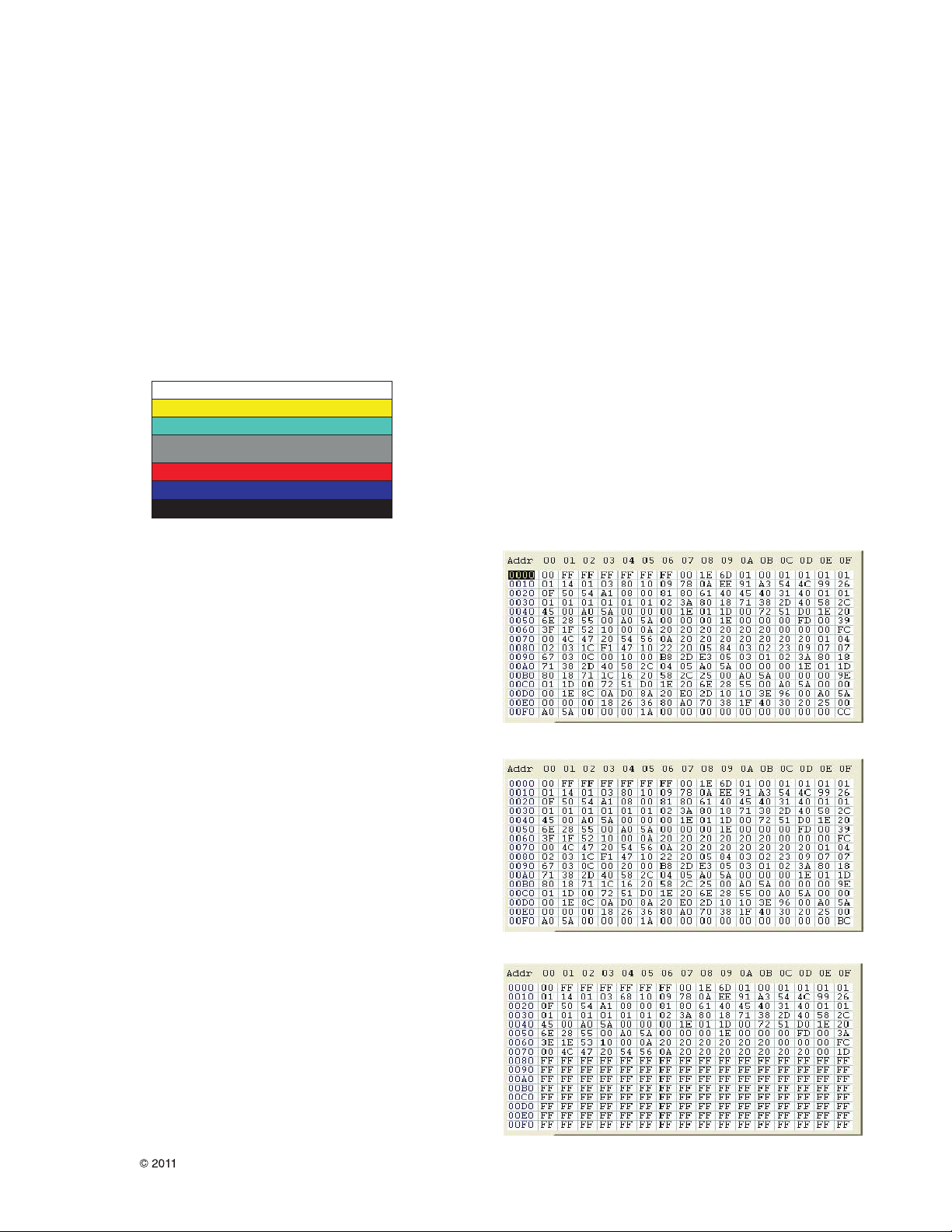
5.2.4 EDID DATA
LGE Internal Use OnlyCopyright LG Electronics. Inc. All right reserved.
Only for training and service purposes
HDMI-1 EDID table
HDMI-2 EDID table
Analog (RGB) EDID table
- 12 -
5.3. White Balance Adjustment
(1) Overview
• W/B adj. Objective & How-it-works
- Objective: To reduce each Panel’s W/B deviation
- How-it-works: When R/G/B gain in the OSD is at 192, it
means the panel is at its Full Dynamic
Range. In order to prevent saturation of
Full Dynamic range and data, one of
R/G/B is fixed at 192, and the other two is
lowered to find the desired value.
- Adj. condition : normal temperature
1) Surrounding Temperature: 25±5ºC
2) Warm-up time: About 5 Min
3) Surrounding Humidity: 20% ~ 80%
(2) Equipment
1) Color Analyzer: CA-210 (NCG: CH 9 / WCG: CH12)
2) Adj. Computer(During auto adj., RS-232C protocol is
needed)
3) Adjust Remocon
4) Video Signal Generator MSPG-925F 720p/216-Gray
(Model:217, Pattern:78)
-> Only when internal pattern is not available
• Color Analyzer Matrix should be calibrated using CS-1000
(3) Equipment connection MAP
(4) Adj. Command (Protocol)
1) RS-232C Command used during auto-adj.
Ex) wb 00 00 -> Begin white balance auto-adj.
wb 00 10 -> Gain adj.
ja 00 ff -> Adj. data
jb 00 c0
...
...
wb 00 1f -> Gain adj. complete
*(wb 00 20(start), wb 00 2f(end)) -> Off-set adj.
wb 00 ff -> End white balance auto adj.
2) Adjustment Map
Applied Model : LA06A Chassis All models.
(5) Auto adj. method
1) Set TV in adj. mode using POWER ON key
2) Zero calibrate probe then place it on the center of the
Display
3) Connect Cable(RS-232C)
4) Select mode in adj. Program and begin adj.
5) When adj. is complete (OK Sing), check adj. status pre
mode (Warm, Medium, Cool)
6) Remove probe and RS-232C cable to complete adj.
* W/B Adj. must begin as start command “wb 00 00” , and
finish as end command “wb 00 ff”, and Adj. offset if need
(6) Manual adj. method
1) Set TV in Adj. mode using POWER ON
2) Zero Calibrate the probe of Color Analyzer, then place
it on the center of LCD module within 10cm of the
surface..
3) Press ADJ key -> EZ adjust using adj. R/C > 6. WhiteBalance then press the cursor to the right (KEY
G).
(When KEY(
G) is pressed 216 Gray internal pattern
will be displayed)
4) One of R Gain / G Gain / B Gain should be fixed at
192, and the rest will be lowered to meet the desired
value.
5) Adj. is performed in COOL, MEDIUM, WARM 3 modes
of color temperature.
- If internal pattern is not available, use RF input. In EZ
Adj. menu 6.White Balance, you can select one of 2
Test-pattern: ON, OFF. Default is inner(ON). By
selecting OFF, you can adjust using RF signal in 216
Gray pattern.
LGE Internal Use OnlyCopyright LG Electronics. Inc. All right reserved.
Only for training and service purposes
Colo r Analyzer
Comp ut er
Pattern Ge n e r ator
RS-232C
RS-232C
RS-232C
Probe
Signal Source
* If TV internal pattern is used, not needed
Connection Diagram of Automatic Adjustment
RS-232C COMMAND
Meaning
[CMD ID DATA]
wb 00 00 Begin White Balance adj.
wb 00 ff End White Balance adj.(Internal pattern disappeared)
ITEM Command Data Range Default
(Hex.) (Decimal)
Cmd 1 Cmd 2 Min Max
Cool R-Gain j g 00 C0
G-Gain j h 00 C0
B-Gain j i 00 C0
R-Cut
G-Cut
B-Cut
Medium R-Gain j a 00 C0
G-Gain j b 00 C0
B-Gain j c 00 C0
R-Cut
G-Cut
B-Cut
Warm R-Gain j d 00 C0
G-Gain j e 00 C0
B-Gain j f 00 C0
R-Cut
G-Cut
- 13 -
* Adj. condition and cautionary items
1) Lighting condition in surrounding area
Surrounding lighting should be lower 10 lux. Try to
isolate adj. area into dark surrounding.
2) Probe location
- LCD: Color Analyzer (CA-210) probe should be
within 10cm and perpendicular of the module
surface (80°~ 100°)
3) Aging time
- After Aging Start, Keep the Power ON status during 5
Minutes.
- In case of LCD, Back-light on should be checked
using no signal or Full-white pattern.
(7) Reference (White Balance Adj. coordinate and color
temperature)
• Luminance: 216 Gray
• Standard color coordinate and temperature using CS-
1000
• Standard color coordinate and temperature using CA210(CH 14)
5.4. HDCP (High-Bandwidth Digital
Contents Protection) SETTING
- HDCP setting is not necessary in This Chassis.
5.5 Option selection per country
5.5.1 Overview
• Option selection is only done for models in Non-USA North
America due to rating
• Applied model: LA06A Chassis applied None USA
model(CANADA, MEXICO)
5.5.2 Method
1) Press ADJ key on the Adj. R/C, then select Country
Group Meun
2) Depending on destination, select KR or US, then on the
lower Country option, select US, CA, MX. Selection is
done using +, - KEY
5.6 Tool Option selection
• Method : Press Adj. key on the Adj. R/C, then select Tool
option.
5.7 hip-out mode check (In-stop)
• After final inspection, press In-Stop key of the Adj. R/C and
check that the unit goes to Stand-by mode.
• After final inspection, Always turn on the Mechanical S/W.
LGE Internal Use OnlyCopyright LG Electronics. Inc. All right reserved.
Only for training and service purposes
Mode Color Coordination Temp ∆UV
xy
COOL 0.269 0.273 11000K 0.0000
MEDIUM 0.285 0.293 9300K 0.0000
WARM 0.313 0.329 6500K 0.0000
Mode Color Coordination Temp ∆UV
xy
COOL 0.269±0.002 0.273±0.002 13000K 0.0000
MEDIUM 0.285±0.002 0.293±0.002 9300K 0.0000
WARM 0.313+0.002 0.329±0.002 6500K 0.0000
Model Tool 1 Tool 2 Tool 3 Tool 4 Tool 5
32LD320H-UA 16864 8786 32772 2305 0
37LD320H-UA 20960 8786 32772 2305 0
42LD320H-UA 25056 8786 32772 2305 0
26LD320H-UA 12768 8786 32772 2305 0
- 14 -
6. GND and Internal Pressure check
6.1. Method
1) GND & Internal Pressure auto-check preparation
- Check that Power Cord is fully inserted to the SET.
(If loose, re-insert)
2) Perform GND & Internal Pressure auto-check
- Unit fully inserted Power cord, Antenna cable and A/V arrive to the auto-check process.
- Connect D-terminal to AV JACK TESTER
- Auto CONTROLLER(GWS103-4) ON
- Perform GND TEST
- If NG, Buzzer will sound to inform the operator.
- If OK, changeover to I/P check automatically.
(Remove CORD, A/V form AV JACK BOX)
- Perform I/P test
- If NG, Buzzer will sound to inform the operator.
- If OK, Good lamp will lit up and the stopper will allow the pallet to move on to next process.
6.2. Checkpoint
• TEST voltage
- GND: 1.5KV/min at 100mA
- SIGNAL: 3KV/min at 100mA
• TEST time: 1 second
• TEST POINT
- GND TEST = POWER CORD GND & SIGNAL CABLE METAL GND
- Internal Pressure TEST = POWER CORD GND & LIVE & NEUTRAL
• LEAKAGE CURRENT: At 0.5mArms
7. Audio
Measurement condition:
1. RF input : Mono, 1KHz sine wave signal, 100% Modulation
2. CVBS, Component : 1KHz sine wave signal 0.4Vrms
3. RGB PC : 1KHz sine wave signal 0.7Vrms
LGE Internal Use OnlyCopyright LG Electronics. Inc. All right reserved.
Only for training and service purposes
No Item Min Typ Max Unit Remark
1.
Audio practical max
9.0 10.0 12.0 W Measurement 32/37/42LD320H-UA
Output, L/R 8.5 8.9 9.8 Vrms condition
(Distortion=10% 6.3 7.0 8.4 W EQ Off 26LD320H-UA
max Output) 7.09 7.48 8.19 Vrms AVL Off
Clear Voice Off
2. Speaker (8Ω 10.0 15.0 W Measurement 32/37/42LD320H-UA
Impedance) 5.0 15.0 W condition 26LD320H-UA
EQ Off
AVL Off
Clear Voice Off
- 15 -
8. Etc
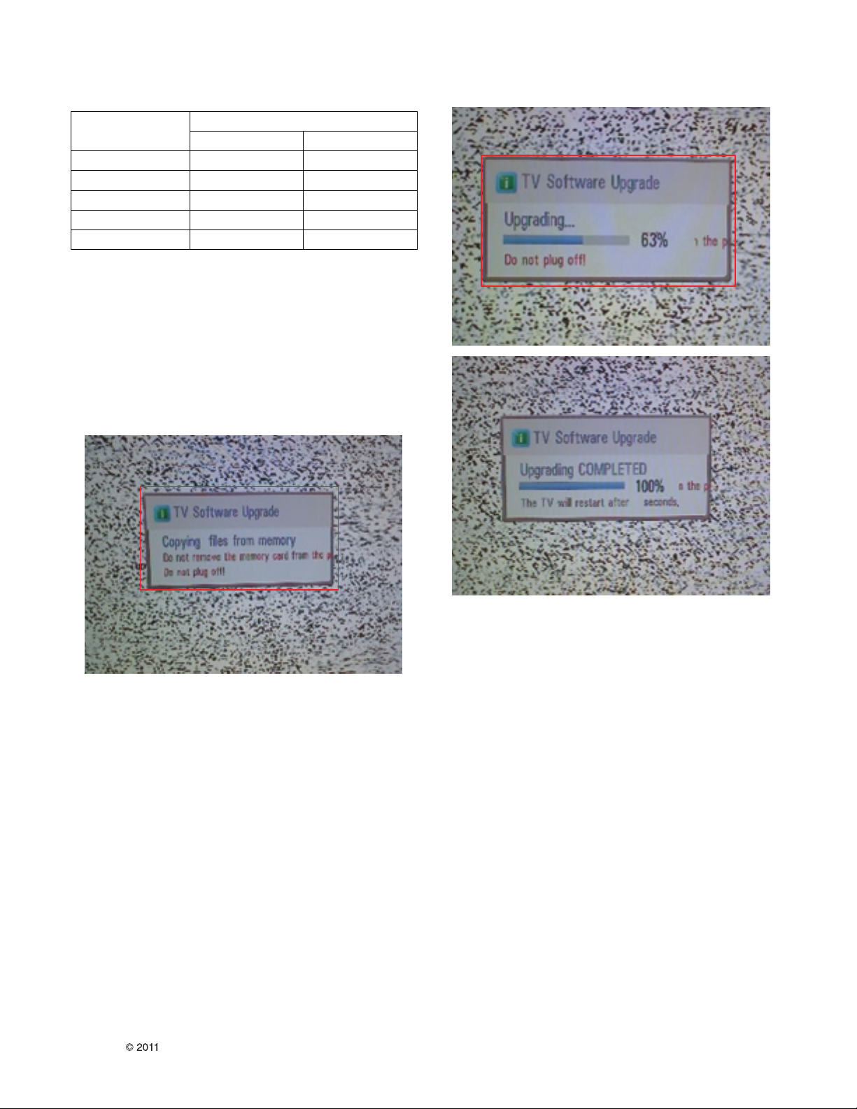
9. USB S/W Download (option)
(1) Put the USB Stick to the USB socket
(2) Automatically detecting update file in USB Stick
- If your downloaded program version in USB Stick is Low,
it didn’t work.
But your downloaded version is High, USB data is
automatically detecting
(3) Show the message “Copying files from memory”
(4) Updating is staring.
(5) Updating Completed, The TV will restart automatically
(6) If your TV is turned on, check your updated version and
Tool option. (explain the Tool option, next stage)
* If downloading version is more high than your TV have,
TV can lost all channel data. In this case, you have to
channel recover. if all channel data is cleared, you didn’t
have a DTV/ATV test on production line.
* After downloading, have to adjust TOOL OPTION again.
1) Push "IN-START" key in service remote controller.
2) Select "Tool Option 1" and Push “OK” button.
3) Punch in the number. (Each model has their number.)
LGE Internal Use OnlyCopyright LG Electronics. Inc. All right reserved.
Only for training and service purposes
Power Status
Main B/D Shipping Condition
AC Swithch condtion
Chassis Module Assembly
ON N/A
Front Module Assembly
N/A OFF
Factory incoming ON OFF
Final Assembly ON ON
Ship-Out OFF ON
- 16 -
10. Test factor for commercial model
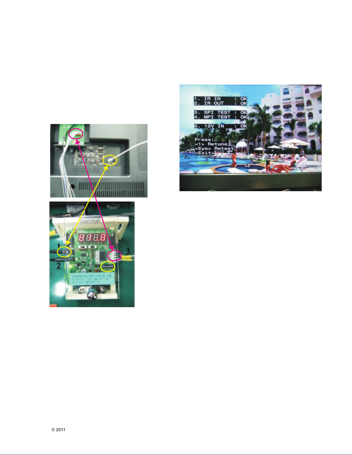
10.1 IR IN/Out, Lodgenet Check
10.1.1 Check Order “OK” Judgment
1) The method of Cable connecting from jig to TV.
a) Power Cable is connected to jig for supplying
voltage. (as below picture point2)
b) Phone jack is Connected for IR out test from TV
REMOTE CONTROL OUT(JK900) to jig. (as below
picture point1)
c) In the right side of check jig, 11pin SPI/MPI signal
cable is connected to MPI dummy board. (as below
picture point3)
2) Test sequence
a) Press EYE using adjust remote-control.
b) Then, tuning the channel 96- 1.(Lodgenet digital1.)
automatically.
c) Check it whether the video is clear and 1~5 factor
“OK” like below picture.
(IR IN / IR OUT / SPI TEST / MPI TEST / 12V IN)
If you find any problem, press <Eye> button and retest.
10.1.2 Needs JIG & Equip. & Cable
1) adjust remote-control
2) commercial check jig & adapter
3) 11 pin cable
4) Phone jack Cable
10.2 Auto camport test
After D-box on, AC power Off and On.
When available AV signal comes to side AV jack, input
mode changing to AV2 automatically.
LGE Internal Use OnlyCopyright LG Electronics. Inc. All right reserved.
Only for training and service purposes
IR IN
Power
MPI/SPI
SIGNAL 11P
No.3 Pin on
nSPI mode
- 17 -
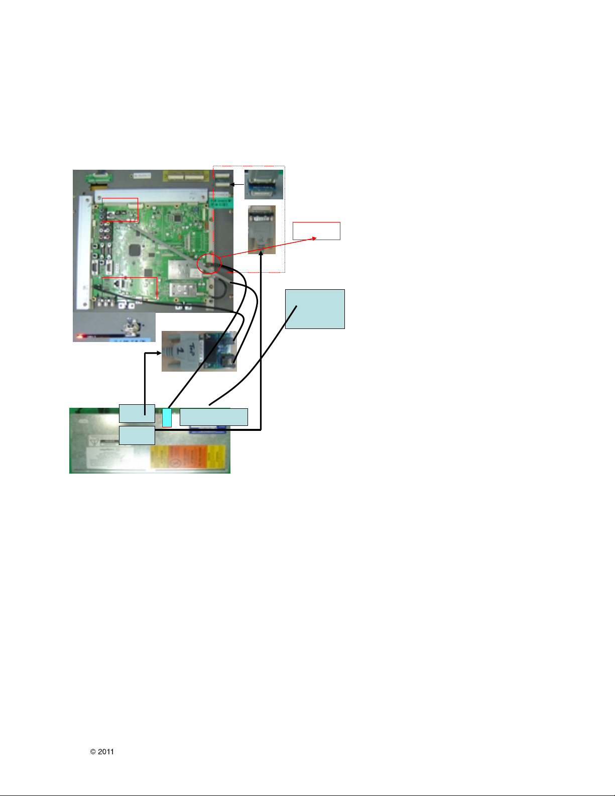
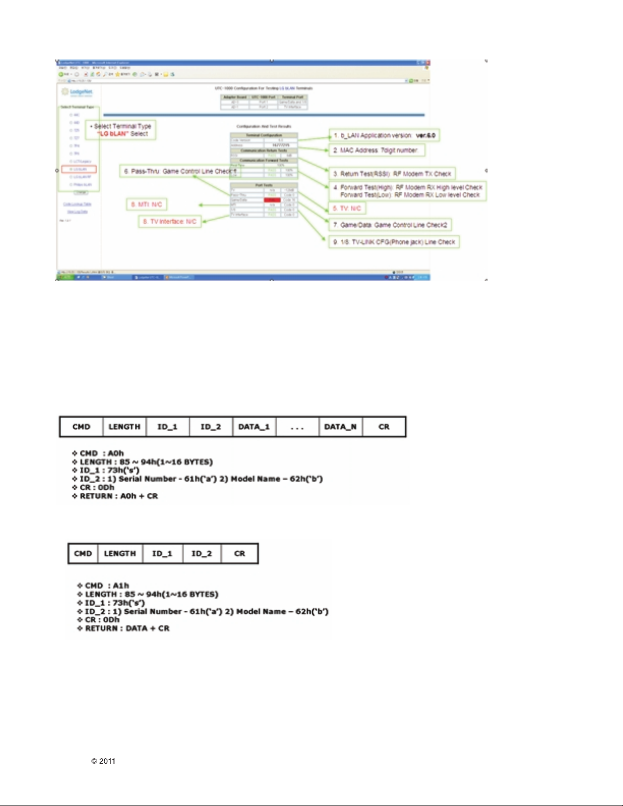
10.3 b_LAN Main board Check
10.3.1 Overview
It is LNET RF modem & FTG card
10.3.2 Equipment
1) b_LAN Checker: UTC-1000 (with Cable accessory)
2) Computer(for test result monitoring)
3) Connection JIG
10.3.3 Equipnent connection map & b_LAN Check
4) Check
=========================================
1. Setting Procedure
1) Setting JIG
(1) Connect UTC-1000 Equipment to JIG device as a like left picture
- Connection Line:
UTC-1000 TOP1 <--> Game port(RJ21)
-> TV-LINK CFG (Phone Jack)
UTC-1000 TOP2 <--> JIG 11pin Connection
UTC-1000 RF1 <--> b_LAN RF IN
UTC-1000 LAN <--> PC LAN Port
2. Working procedure
1) Connection
UTC-1000 LAN <--> PC LAN Port
UTC-1000 TOP1 <--> Game port(RJ21)
-> TV-LINK CFG (Phone Jack)
UTC-1000 RF1 <--> b_LAN RF IN
2) Power on JIG
3) Test Start
UTC-1000 TOP2 <--> JIG 11pin Connection
4) Checking b-LAN MAC Address
Check whether it is same their address numbers or not between B-LAN Label and on the pc address numbers.
LGE Internal Use OnlyCopyright LG Electronics. Inc. All right reserved.
Only for training and service purposes
TOP1
TOP2
RF1
Power
TOP
AC 110V
UTC-1000
LAN PORT
Computer LA N
PORT
b_LAN RF IN
RJ12
Phone Jack (2)
- 18 -
* Checking JIG contents
1. Check whether displaying all “Pass” or not at the number 3.4.6.7.9 contents of UTC-1000 on the PC
2. Check “Version 6.0” of the 1. b_LAN Application version
3. Check whether it is same their address numbers or not between B-LAN Label and 2. MAC Address on the pc.
11. Serial number download.
Connect Bar Code scan equipment and TV set by RS-232C cable.
1) E2PROM Data Write
2) E2PROM Data Read
LGE Internal Use OnlyCopyright LG Electronics. Inc. All right reserved.
Only for training and service purposes
LGE Internal Use OnlyCopyright LG Electronics. Inc. All right reserved.
Only for training and service purposes
- 19 -
300
200
801
802
804
805
806
520
530
540
550
400
900
120
510
500
LV1
560
A2
A10
A5
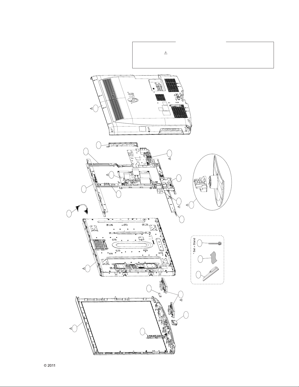
EXPLODED VIEW
Many electrical and mechanical parts in this chassis have special safety-related characteristics. These
parts are identified by in the Schematic Diagram and EXPLODED VIEW.
It is essential that these special safety parts should be replaced with the same components as
recommended in this manual to prevent X-RADIATION, Shock, Fire, or other Hazards.
Do not modify the original design without permission of manufacturer.
IMPORTANT SAFETY NOTICE
FPGA POWER
+3.3V_Normal
L1227
MLB-201209-0120P-N2
RESET
012:Q17
FPGA_RESET
27MHz
012:Q17
DE_H_SYSCLK
I2C
AMP_SCL
MSCL_3.3V
FE_DEMOD_SCL
001:AG5;002:S20
AMP_SDA
MSDA_3.3V
FE_DEMOD_SDA
001:AG5;002:S20
3.3V_Proidiom
VSB_RESET
C2176
10uF
16V
R2385
R2386
0
0
3.3V_Proidiom
OPT
R2390
10K
4.7K
R2563
3.3V_Proidiom
OPT
OPT
C2177
100uF
16V
3.3V_Proidiom
C2179
OPT
C2178
0.1uF
16V
22R2387
0
0
0
0
MLB-201209-0120P-N2
L1228
1N4148W
D1250
OPT
R2393
100
OPT
R2394
1uF
100
25V
OPT
100
R2564
RESET
temp
27MHz
6
3.3V_Proidiom
10K
R2391
R2446
R2447
3.3V_Proidiom
10K
R2392
R2448
R2449
X1006
Q1114
BSS83
Q1115
BSS83
IC1210
MAX809RTR
2
1
25
34
D
B
S
D
B
S
012:S26;012:AJ26
+VCCINT_1.5V
VCC
3
1
GND
G
G
C2255
1uF
25V
012:B17
VSB_RESET
001:AJ21
SYS_RESET
3.3V_Proidiom
+5V_Normal
C2180
0.1uF
16V
OPT
C2181
0.1uF
16V
OPT
FPGA
3.3V_Proidiom
+VCCINT_1.5V
MLB-201209-0120P-N2
16V
GNDA_PLL2
GNDG_PLL2
J11
J12
L1231
0.1uF
0.01uFC2191
16V
C2190
GND_25
GND_26J6GNDA_PLL1
GNDG_PLL1
J5
T16
T12
M6
IO4_10N5IO4_11N6IO4_12R6IO4_14M7IO4_15T6IO4_16R7IO4_17N7IO4_19T8IO4_21M8IO4_22N8IO4_23
1uF
C2192
GND_22T1GND_23T5GND_24
L11
0.1uF
0.1uF
0.1uF
0.1uF
0.1uF
16V
16V
C2199
C2198
VCCIO3_1
VCCIO3_2
P16
K11
0.1uF
0.1uF
16V
16V
C2200
C2201
VCCIO4_3
VCCIO4_4
L10
T14
0.1uF
16V
16V
C2202
C2203
VCCIO4_1
VCCIO4_2
T3
L7
0.1uF
16V
16V
C2205
C2204
VCCIO1_2
VCCIO1_3
P1
G6
0.1uF
16V
16V
C2207
C2206
VCCINT_12
VCCIO1_1
C1
T10
0.1uF
16V
C2208
VCCINT_11
T7
0.1uF
0.1uF
0.1uF
0.1uF
0.1uF
16V
16V
16V
16V
C2193
C2197
C2196
C2194
50V
GND_4F6GND_5F8GND_6F9GND_7
GND_8G7GND_9G9GND_10
GND_11H8GND_12
GND_13J7GND_14J9GND_15K6GND_16K8GND_17
GND_18L6GND_19L8GND_20L9GND_21
F11
G11
H10
K10
A12
C2195
VCCIO3_3
VCCIO2_1
VCCIO2_2
VCCIO2_3
VCCIO2_4
GND_1
GND_2A5GND_3
F7
A3
A1
F10
C16
A14
A16
IC1209
LGDT1129
M10
T11
N10
N11
N12
M11
M12
R12
T13
R13
R14
P13
T15
R15
N13
P14
P15
R16
N15
N16
K12
K14
L12
N14
M13
IO3_1
IO3_2
IO3_3
IO3_4
IO3_5
IO3_6
IO3_7
IO3_8
IO4_25T9IO4_27N9IO4_29
IO4_31
IO4_32
IO4_36
IO4_37M9IO4_38
IO4_39
IO4_40
0R2425
IO4_42
IO4_43
IO4_44
IO4_45
IO4_46
IO4_47
IO4_48
IO3_9
IO3_10
IO3_11
0.1uF
0.1uF
16V
16V
C2210
C2209
VCCINT_9
VCCINT_10
K7
K9
M14
L13
IO3_12
IO3_13
R2426
0
0.1uF
0.1uF
16V
16V
C2211
C2212
VCCINT_7
VCCINT_8
J8
J10
M15
M16
IO3_14
IO3_15
0.1uF
0.1uF
16V
16V
C2214
C2213
VCCINT_5
VCCINT_6
H7
H9
L14
L15
IO3_16
IO3_17
0.1uF
0.1uF
16V
16V
C2215
C2216
VCCINT_3
VCCINT_4
G8
G10
L16
K16
IO3_18
IO3_19
0.1uF
0.1uF
16V
16V
C2217
C2218
VCCINT_1
VCCINT_2
A7
A10
K15
J16
IO3_20
IO3_21
16V
IO4_34/CH_CLK
R11
IO4_20/CH_VALID
R8
IO4_26/CH_SOP
R9
IO4_30/CH_ERR
R10
IO4_8/CH_DATA[0]
P5
IO4_13/CH_DATA[1]
P6
IO4_18/CH_DATA[2]
P7
IO4_24/CH_DATA[3]
P8
IO4_28/CH-DATA[4]
P9
IO4_33/CH_DATA[5]
P10
IO4_35/CH_DATA[6]
P11
IO4_41/CH_DATA[7]
P12
IO2_34
E7
IO2_33
A6
IO2_32
B7
IO2_43
A4
IO2_30
D7
IO2_28
A8
IO2_27
E8
IO2_26
D8
IO2_44
B4
IO2_24
E10
IO2_45
C4
IO2_22
D9
IO2_20
A9
IO2_19
D10
IO2_16
A11
IO2_15
B11
IO2_46
B3
IO2_13
D11
IO2_12
D12
IO2_11
E9
IO2_10
E11
IO2_9
E12
IO2_47
A2
IO2_7
B12
IO2_6
A13
IO2_5
B13
IO2_4
C13
IO2_3
B14
IO2_2
A15
IO2_1
B15
IO3_43
D13
IO3_42
C14
IO3_41
C15
IO3_40
B16
IO3_39
G12
IO3_38
H13
IO3_36
E13
IO3_35
F12
IO3_33
D15
IO3_32
D16
IO3_31
E15
IO3_30
E16
IO3_29
F15
IO3_28
F13
IO3_27
F14
IO3_26
F16
IO3_25
G15
IO3_24
G13
IO3_23
G14
IO3_22
H12
CLK2
G16
CLK3
H16
L1232
MLB-201209-0120P-N2
0R2431
MLB-201209-0120P-N2
L1230
0.1uF
C2186
16V
50V
H1
B8
B9
B10
C5
C6
C7
C8
C9
C10
C11
C12
M1
C3
C2
B1
G5
F4
D3
E4
F5
E3
D2
E2
G1
B2
D14
E14
K4
K13
H3
J4
H2
G4
K3
H4
J13
J3
J2
J14
H15
J15
H14
D4
D1
F3
G3
F2
E1
G2
F1
H5
J1
K2
L3
K1
L1
L2
N1
M2
N2
M3
L5
M4
N3
IO1_36K5IO1_37L4IO1_38R1IO1_39P2IO1_40P3IO1_41N4IO1_42
C2187
0.01uFC2188
16V
IO2_35B5IO2_42D6IO2_37D5IO2_38E6IO2_39E5IO2_40
C2189
4.7uF
VCCA_PLL1
VCCA_PLL2
B6
H6
H11
R2
IO4_1T2IO4_2R3IO4_3P4IO4_4R4IO4_5T4IO4_6R5IO4_7M5IO4_9
1uF
0R2424
IO2_29/TP_SOP
IO2_17/TP_ERR
IO1_29
IO1_10
IO1_11
IO1_12
IO2_48/RESET
IO3_37/I2C_SCK
IO3_34/I2C_SDA
DCLK
CONF_DONE
NCONFIG
DATA0
IO1_21SO
IO1_22/ASDO
NCEO
NSTATUS
MSEL0
MSEL1
IO1_13
IO1_14
IO1_15
IO1_16
IO1_17
IO1_18
IO1_19
IO1_20
IO1_23
IO1_24
IO1_25
IO1_26
IO1_27
IO1_28
IO1_30
IO1_31
IO1_32
IO1_33
IO1_34
IO1_35
0
CLK1
IO1_2
IO1_3
IO1_4
IO1_5
IO1_6
IO1_7
IO1_8
IO1_9
CLK0
NCE
TCK
TDO
TMS
4.7uF
C2185
TDI
3.3V_Proidiom
0
OPT
R2418
IO2_21/TP_VALID
IO2_41/TP_DATA[7]
IO2_36/TP_DATA[6]
IO2_31/TP_DATA[5]
IO2_25/TP_DATA[4]
IO2_23/TP_DATA[3]
IO2_18/TP_DATA[2]
IO2_14/TP_DATA[1]
IO2_8/TP_DATA[0]
10K
R2422
GND
0
R2420
10K
22R2415
22R2416
22R2417
10KR2412
10KR2413
10KR2414
10KR2409
IO1_1/INIT_DONE
10KR2408
R2421
0
OPT
R2419
0
R2423
TS_0
TS_1
TS_2
TS_3
TS_4
TS_5
TS_6
TS_7
3.3V_Proidiom
TS_CLK
TS_VALID
TS_SYNC
R2399
0
012:C13
012:B19
3.3V_Proidiom
DE_H_SYSCLK
FPGA_RESET
MSCL_3.3V
MSDA_3.3V
R2401
0
3.3V_Proidiom
R2406
GND
1K
R2402
1K
R2403
1K
R2404
R2405
OPT
001:AJ17
001:AJ16
001:AJ16
001:AJ16
001:AJ16
001:AJ15
001:AJ15
001:AJ15
001:AJ15
001:AJ15
001:AJ14
1K
R2397
TS_0
TS_1
TS_4
TS_2
TS_3
TS_5
TS_6
TS_7
+VCCINT_1.5V
L1235
L1233
L1234
L1236
MLB-201209-0120P-N2
MLB-201209-0120P-N2
MLB-201209-0120P-N2
MLB-201209-0120P-N2
OPT
C2219
62pF
50V
100R2441
100R2442
100R2443
100R2444
PM_TS[0]
PM_TS[1]
PM_TS[2]
PM_TS[3]
PM_TS[4]
PM_TS[5]
PM_TS[6]
PM_TS[7]
INNER LAYER PATERN
0R2435
0R2436
001:AJ19
PM_TS_CLK
001:AJ19
PM_TS_VALID
001:AJ19
PM_TS_SYNC
001:AJ19
PM_TS[0-7]
THE SYMBOL MARK OF THIS SCHEMETIC DIAGRAM INCORPORATES
SPECIAL FEATURES IMPORTANT FOR PROTECTION FROM X-RADIATION.
FILRE AND ELECTRICAL SHOCK HAZARDS, WHEN SERVICING IF IS
ESSENTIAL THAT ONLY MANUFATURES SPECFIED PARTS BE USED FOR
THE CRITICAL COMPONENTS IN THE SYMBOL MARK OF THE SCHEMETIC.
LD320H-UA_LA06A
FPGA
2010.09.04
12(11)
21
 Loading...