

Page 1

Internal Use Only
US/Canada/Mexico http://aic.lgservice.com
http://eic.lgservice.com
http://biz.lgservice.com
LED TV
SERVICE MANUAL
CHASSIS : 6M62N
MODEL: 32LB520B
CAUTION
BEFORE SERVICING THE CHASSIS,
READ THE SAFETY PRECAUTIONS IN THIS MANUAL.
Printed in Korea
Page 2

CONTENTS
CONTENTS .............................................................................................. 2
SAFETY PRECAUTIONS ........................................................................ 3
SERVICING PRECAUTIONS ................................................................... 4
SPECIFICATION ...................................................................................... 6
ADJUSTMENT INSTRUCTION ............................................................... 8
EXPLODED VIEW .................................................................................. 13
SCHEMATIC CIRCUIT DIAGRAM ..........................................................
14
Only for training and service purposes
- 2 -
LGE Internal Use OnlyCopyright © LG Electronics. Inc. All rights reserved.
Page 3
SAFETY PRECAUTIONS
IMPORTANT SAFETY NOTICE
Many electrical and mechanical parts in this chassis have special safety-related characteristics. These parts are identified by in the
Schematic Diagram and Exploded View.
It is essential that these special safety parts should be replaced with the same components as recommended in this manual to prevent
Shock, Fire, or other Hazards.
Do not modify the original design without permission of manufacturer.
General Guidance
An isolation Transformer should always be used during the
servicing of a receiver whose chassis is not isolated from the AC
power line. Use a transformer of adequate power rating as this
protects the technician from accidents resulting in personal injury
from electrical shocks.
It will also protect the receiver and it's components from being
damaged by accidental shorts of the circ uitry that may be
inadvertently introduced during the service operation.
If any fuse (or Fusible Resistor) in this TV receiver is blown,
replace it with the specified.
When replacing a high wattage resistor (Oxide Metal Film Resistor,
over 1 W), keep the resistor 10 mm away from PCB.
Keep wires away from high voltage or high temperature parts.
Before returning the receiver to the customer,
always perform an AC leakage current check on the exposed
metallic parts of the cabinet, such as antennas, terminals, etc., to
be sure the set is safe to operate without damage of electrical
shock.
Leakage Current Cold Check(Antenna Cold Check)
With the instrument AC plug removed from AC source, connect an
electrical jumper across
switch in the on position, connect one lead of ohm-meter to the AC
plug prongs tied together and touch other ohm-meter lead in turn to
each exposed metallic parts such as antenna terminals, phone
jacks, etc.
If the exposed metallic part has a return path to the chassis, the
measured resistance should be between 10 MΩ and 200 MΩ.
When the exposed metal has no return path to the chassis the
reading must be infinite.
An other abnormality exists that must be corrected before the
receiver is returned to the customer.
the two AC plug prongs. Place the AC
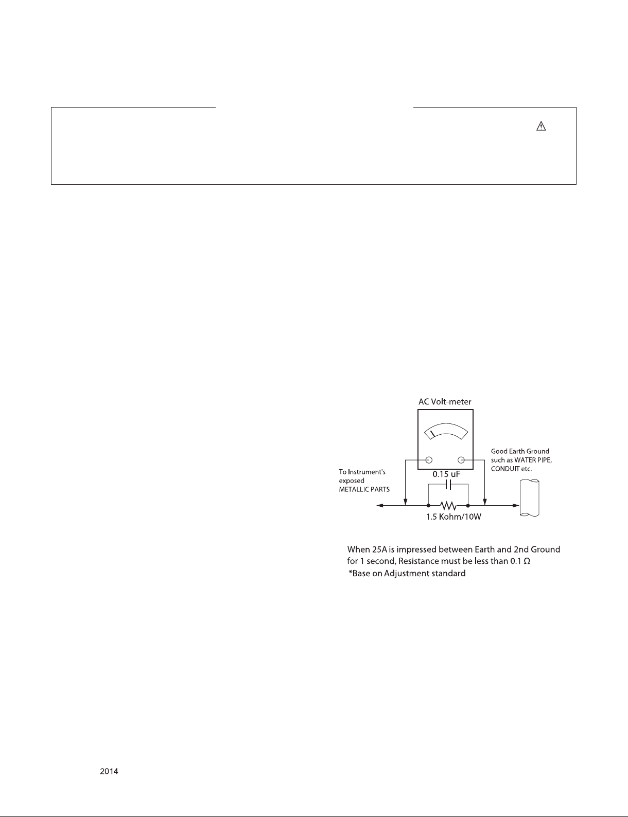
Leakage Current Hot Check (See below Figure)
Plug the AC cord directly into the AC outlet.
Do not use a line Isolation Transformer during this check.
Connect 1.5 K / 10 watt resistor in parallel with a 0.15 uF capacitor
between a known good earth ground (Water Pipe, Conduit, etc.)
and the exposed metallic parts.
Measure the AC voltage across the resistor using AC voltmeter
with 1000 ohms/volt or more sensitivity.
Reverse plug the AC cord into the AC outlet and repeat AC voltage
measurements for each exposed metallic part. Any voltage
measured must not exceed 0.75 volt RMS which is corresponds to
0.5 mA.
In case any measurement is
possibility of shock hazard and the set must be checked and
repaired before it is returned to the customer.
out of the limits specified, there is
Leakage Current Hot Check circuit
Only for training and service purposes
- 3 -
LGE Internal Use OnlyCopyright © LG Electronics. Inc. All rights reserved.
Page 4

SERVICING PRECAUTIONS
CAUTION: Before servicing receivers covered by this service
manual and its supplements and addenda, read and follow the
SAFETY PRECAUTIONS on page 3 of this publication.
NOTE: If unforeseen circumstances create conict between the
following servicing precautions and any of the safety precautions
on page 3 of this publication, always follow the safety precautions. Remember: Safety First.
General Servicing Precautions
1. Always unplug the receiver AC power cord from the AC power
source before;
a. Removing or reinstalling any component, circuit board
module or any other receiver assembly.
b. Disconnecting or reconnecting any receiver electrical plug
or other electrical connection.
c. Connecting a test substitute in parallel with an electrolytic
capacitor in the receiver.
CAUTION: A wrong part substitution or incorrect polarity
installation of electrolytic capacitors may result in an explosion hazard.
2. Test high voltage only by measuring it with an appropriate
high voltage meter or other voltage measuring device (DVM,
FETVOM, etc) equipped with a suitable high voltage probe.
Do not test high voltage by "drawing an arc".
3. Do not spray chemicals on or near this receiver or any of its
assemblies.
4. Unless specied otherwise in this service manual, clean
electrical contacts only by applying the following mixture to the
contacts with a pipe cleaner, cotton-tipped stick or comparable
non-abrasive applicator; 10 % (by volume) Acetone and 90 %
(by volume) isopropyl alcohol (90 % - 99 % strength)
CAUTION: This is a ammable mixture.
Unless specied otherwise in this service manual, lubrication
of contacts in not required.
5. Do not defeat any plug/socket B+ voltage interlocks with which
receivers covered by this service manual might be equipped.
6. Do not apply AC power to this instrument and/or any of its
electrical assemblies unless all solid-state device heat sinks
are correctly installed.
7. Always connect the test receiver ground lead to the receiver
chassis ground before connecting the test receiver positive
lead.
Always remove the test receiver ground lead last.
8. Use with this receiver only the test xtures specied in this
service manual.
CAUTION: Do not connect the test xture ground strap to any
heat sink in this receiver.
Electrostatically Sensitive (ES) Devices
Some semiconductor (solid-state) devices can be damaged easily by static electricity. Such components commonly are called
Electrostatically Sensitive (ES) Devices. Examples of typical ES
devices are integrated circuits and some eld-effect transistors
and semiconductor “chip” components. The following techniques
should be used to help reduce the incidence of component damage caused by static by static electricity.
1. Immediately before handling any semiconductor component or
semiconductor-equipped assembly, drain off any electrostatic
charge on your body by touching a known earth ground. Alternatively, obtain and wear a commercially available discharging wrist strap device, which should be removed to prevent
potential shock reasons prior to applying power to the unit
under test.
2. After removing an electrical assembly equipped with ES
devices, place the assembly on a conductive surface such as
aluminum foil, to prevent electrostatic charge buildup or exposure of the assembly.
3. Use only a grounded-tip soldering iron to solder or unsolder
ES devices.
4. Use only an anti-static type solder removal device. Some solder removal devices not classied as “anti-static” can generate
electrical charges sufcient to damage ES devices.
5. Do not use freon-propelled chemicals. These can generate
electrical charges sufcient to damage ES devices.
6. Do not remove a replacement ES device from its protective
package until immediately before you are ready to install it.
(Most replacement ES devices are packaged with leads electrically shorted together by conductive foam, aluminum foil or
comparable conductive material).
7. Immediately before removing the protective material from the
leads of a replacement ES device, touch the protective material to the chassis or circuit assembly into which the device will
be installed.
CAUTION: Be sure no power is applied to the chassis or circuit, and observe all other safety precautions.
8. Minimize bodily motions when handling unpackaged replacement ES devices. (Otherwise harmless motion such as the
brushing together of your clothes fabric or the lifting of your
foot from a carpeted oor can generate static electricity sufcient to damage an ES device.)
General Soldering Guidelines
1. Use a grounded-tip, low-wattage soldering iron and appropriate tip size and shape that will maintain tip temperature within
the range or 500 °F to 600 °F.
2. Use an appropriate gauge of RMA resin-core solder composed
of 60 parts tin/40 parts lead.
3. Keep the soldering iron tip clean and well tinned.
4. Thoroughly clean the surfaces to be soldered. Use a mall wirebristle (0.5 inch, or 1.25 cm) brush with a metal handle.
Do not use freon-propelled spray-on cleaners.
5. Use the following unsoldering technique
a. Allow the soldering iron tip to reach normal temperature.
(500 °F to 600 °F)
b. Heat the component lead until the solder melts.
c. Quickly draw the melted solder with an anti-static, suction-
type solder removal device or with solder braid.
CAUTION: Work quickly to avoid overheating the circuit
board printed foil.
6. Use the following soldering technique.
a. Allow the soldering iron tip to reach a normal temperature
(500 °F to 600 °F)
b. First, hold the soldering iron tip and solder the strand
against the component lead until the solder melts.
c. Quickly move the soldering iron tip to the junction of the
component lead and the printed circuit foil, and hold it there
only until the solder ows onto and around both the component lead and the foil.
CAUTION: Work quickly to avoid overheating the circuit
board printed foil.
d. Closely inspect the solder area and remove any excess or
splashed solder with a small wire-bristle brush.
Only for training and service purposes
- 4 -
LGE Internal Use OnlyCopyright © LG Electronics. Inc. All rights reserved.
Page 5
IC Remove/Replacement
Some chassis circuit boards have slotted holes (oblong) through
cuit foil. When holes are the slotted type, the following technique
should be used to remove and replace the IC. When working with
boards using the familiar round hole, use the standard technique
as outlined in paragraphs 5 and 6 above.
Removal
1. Desolder and straighten each IC lead in one operation by
gently prying up on the lead with the soldering iron tip as the
solder melts.
2. Draw away the melted solder with an anti-static suction-type
solder removal device (or with solder braid) before removing
the IC.
Replacement
1. Carefully insert the replacement IC in the circuit board.
2. Carefully bend each IC lead against the circuit foil pad and
solder it.
3. Clean the soldered areas with a small wire-bristle brush.
(It is not necessary to reapply acrylic coating to the areas).
"Small-Signal" Discrete Transistor
Removal/Replacement
1. Remove the defective transistor by clipping its leads as close
as possible to the component body.
2. Bend into a "U" shape the end of each of three leads remaining on the circuit board.
3. Bend into a "U" shape the replacement transistor leads.
4. Connect the replacement transistor leads to the corresponding
leads extending from the circuit board and crimp the "U" with
long nose pliers to insure metal to metal contact then solder
each connection.
Power Output, Transistor Device
Removal/Replacement
1. Heat and remove all solder from around the transistor leads.
2. Remove the heat sink mounting screw (if so equipped).
3. Carefully remove the transistor from the heat sink of the circuit
board.
4. Insert new transistor in the circuit board.
5. Solder each transistor lead, and clip off excess lead.
6. Replace heat sink.
Diode Removal/Replacement
1. Remove defective diode by clipping its leads as close as possible to diode body.
2. Bend the two remaining leads perpendicularly to the circuit
board.
3. Observing diode polarity, wrap each lead of the new diode
around the corresponding lead on the circuit board.
4. Securely crimp each connection and solder it.
5. Inspect (on the circuit board copper side) the solder joints of
the two "original" leads. If they are not shiny, reheat them and
if necessary, apply additional solder.
3. Solder the connections.
CAUTION: Maintain original spacing between the replaced
-
component and adjacent components and the circuit board to
prevent excessive component temperatures.
Circuit Board Foil Repair
Excessive heat applied to the copper foil of any printed circuit
board will weaken the adhesive that bonds the foil to the circuit
board causing the foil to separate from or "lift-off" the board. The
following guidelines and procedures should be followed whenever this condition is encountered.
At IC Connections
To repair a defective copper pattern at IC connections use the
following procedure to install a jumper wire on the copper pattern
side of the circuit board. (Use this technique only on IC connections).
1. Carefully remove the damaged copper pattern with a sharp
knife. (Remove only as much copper as absolutely necessary).
2. carefully scratch away the solder resist and acrylic coating (if
used) from the end of the remaining copper pattern.
3. Bend a small "U" in one end of a small gauge jumper wire and
carefully crimp it around the IC pin. Solder the IC connection.
4. Route the jumper wire along the path of the out-away copper
pattern and let it overlap the previously scraped end of the
good copper pattern. Solder the overlapped area and clip off
any excess jumper wire.
At Other Connections
Use the following technique to repair the defective copper pattern
at connections other than IC Pins. This technique involves the
installation of a jumper wire on the component side of the circuit
board.
1. Remove the defective copper pattern with a sharp knife.
Remove at least 1/4 inch of copper, to ensure that a hazardous
condition will not exist if the jumper wire opens.
2. Trace along the copper pattern from both sides of the pattern
break and locate the nearest component that is directly connected to the affected copper pattern.
3. Connect insulated 20-gauge jumper wire from the lead of the
nearest component on one side of the pattern break to the
lead of the nearest component on the other side.
Carefully crimp and solder the connections.
CAUTION: Be sure the insulated jumper wire is dressed so then
it does not touch components or sharp edges.
Fuse and Conventional Resistor
Removal/Replacement
1. Clip each fuse or resistor lead at top of the circuit board hollow
stake.
2. Securely crimp the leads of replacement component around
notch at stake top.
Only for training and service purposes
- 5 -
LGE Internal Use OnlyCopyright © LG Electronics. Inc. All rights reserved.
Page 6
SPECIFICATION
NOTE : Specifications and others are subject to change without notice for improvement
.
1. Application range
This specification is applied to the LED TV used
6M62N chassis.
2. Requirement for Test
Each part is tested as below without special appointment.
1) Temperature: 25 °C ± 5 °C(77 °F ± 9 °F), CST: 40 °C ± 5 °C
2) Relative Humidity: 65 % ± 10 %
3) Power Voltage
: Standard input voltage (AC 120V~, 50/60 Hz)
* Standard Voltage of each products is marked by models.
4) Specification and performance of each parts are followed
ea ch drawing and spe ci fication b y p ar t number in
accordance with BOM.
5) ehT receiver must be operated for about 5 minutes prior to
the adjustment.
3. Test method
1) Performance: LGE TV test method followed
2) Demanded other specification
- Safety : UL specification
- EMC : FCC
4. Model General Specification
No. Item Remarks
1. Market US/Canada/Mexico
1) NTSC
2. Broadcasting system
3. Channel Storage 1) VHF : 02~13
2)AIR:ATSC
3)CABLE:64QAM/256QAM
2) UHF : 14~69
3) DTV : 02-69
4) CATV :01~135 (N.America)
5) CADTV : 01~135 (N.America)
4. Receiving system
5. Video(Composite Input) PAL, NTSC 4 System : PAL M, PAL N, NTSC, PAL60
6. Component Input Y/Cb/Cr, Y/Pb/Pr
7. HDMI Input
8. SPDIF out SPDIF out
9. USB Input Music :MP3; Photo: JPEG
10. Headphone
Only for training and service purposes
Analog : Upper Heterodyne
Digital : 8VSB/64&256QAM
HDMI: DTV/DVI
- 6 -
Support HDCP
LGE Internal Use OnlyCopyright © LG Electronics. Inc. All rights reserved.
Page 7
5. Component Video Input (Y, CB /PB , CR /PR )
No. Resolution H-freq(kHz) V-freq(Hz) Porposed
1 720×480 15.73 60.00 SDTV, DVD 480i
2 720×480 15.63 59.94 SDTV, DVD 480i
3 720×480 31.47 59.94 480p
4 720×480 31.50 60.00 480p
1280×720 44.96 59.94 HDTV 720p
5
1280×720 45.00
6
1920×1080
7
1920×1080
8
1920×1080
9
1920×1080
10
11 1920×1080
12 1920×1080
1920×1080
13
14 1920×1080 67.5 60 HDTV 1080p
26.97
27
33.72
33.75
33.75 60.00 HDTV 1080i
33.72
67.432 59.94
60.00 HDTV 720p
23.976
24
29.97
30
59.94 HDTV 1080i
HDTV 1080p
HDTV 1080p
HDTV 1080p
HDTV 1080p
HDTV 1080p
6. HDMI Input : Refer to adjust specification about EDID data.
6.1. DTV mode
No. Resolution H-freq(kHz) V-freq.(kHz) Pixel clock(MHz) Proposed
1. 640*480 31.469 / 31.5 59.94 / 60 25.175/25.200 SDTV 480P
2.
3.
4. 1280*720 44.96 / 45 59.94 / 60 74.17/74.25 HDTV 720P
5. 1920*1080 33.72 / 33.75 59.94 / 60 74.17/74.25 HDTV 1080I
6.
7.
8.
720*480 31.469 / 31.5 59.94 / 60 27.00/27.03 SDTV 480P
720(1440)*480 15.73 / 15.75 59.94 / 60 27.00/27.028 SDTV 480i
1920*1080 26.97 / 27 23.97 / 24 74.17/74.25 HDTV 1080P
1920*1080 33.716/33.75 29.976/30.00 74.25 HDTV 1080P
1920*1080 67.43 / 67.5 59.94 / 60 148.35/148.50 HDTV 1080P
6.2. PC mode
No. Resolution H-freq(kHz) V-freq.(Hz) Pixel clock(MHz) Proposed Remark
1.
720*400 @70Hz 31.469 70.08 28.321 DOS
2.
640*480 @60Hz 31.469 59.940 25.175 VESA(VGA)
3.
800*600 @60Hz 37.879 60.31 40.000 VESA(SVGA)
4.
1024*768 @60Hz 48.363 60.00 65.000 VESA(XGA)
1280*1024 @60Hz 63.981
5.
1360*768 @60Hz 47.712
6
7.
1920*1080 @60Hz 67.5
Only for training and service purposes
60.020 108 VESA(SXGA)
60.015 85.5 VESA(WXGA)
60.0 148.5
WUXGA
(Reduced blanking)
- 7 -
FHD only(Support to HDMI-PC)
FHD only(Support to HDMI-PC)
LGE Internal Use OnlyCopyright © LG Electronics. Inc. All rights reserved.
Page 8

ADJUSTMENT INSTRUCTION
1. Application Range
This specification sheet is applied to all of the LED TV with
MSD3393LU chassis.
2. Designation
(1) Th e ad justm ent is according to the orde r wh ich is
designated and which must be followed, according to the
plan which can be changed only on agreeing.
(2) Power adjustment : Free Voltage.
(3) Magnetic Field Condition: Nil.
(4) Input signal Unit: Product Specification Standard.
(5) Reserve after operation: Above 5 Minutes (Heat Run)
Temperature : at 25 °C ± 5 °C
Relative humidity : 65 ± 10 %
Input voltage : 120V~, 50/60 Hz
(6) Adjustment equipments
: Color Analyzer(CA-210 or CA-310), Service remote control.
(7) Push the “RESTORE" key - For memory initialization.
Case1 : Software version up
1. , BSU yb W/S gnidaolnwod retfA TV set will reboot
automatically.
2. Push “RESTORE” key.
3. Push “Power on” key.
4. Function inspection
5. After function inspection, Push “RESTORE” key.
Case2 : Function check at the assembly line
1. When TV set is entering on the assembly line, Push
“RESTORE” key at first.
2. Push “Power on” key for turning it on.
→ If you push “Power on” key, TV set will recover
channel information by itself.
3. After function inspection, Push “RESTORE” key.
3. Click “Connect”to get communication from the TV set,
and read out the device type.
:
4. Click “HDCP”to enter HDCP management
interface. Change the Value“HDCP Key Index”
to “1”, “HDCP Key Allocation”to "0X390000"for
32LB520B/60LB5200/65LB5200.
3. Main PCB check process
▪ APC - After Manual-Insert, executing APC
*. Burning HDCP EY
1.
Connect your PC to TV set with USB debug cable.
Turn on the TV set, then open the HDCP operating tool
2.
“MStar IS P Utility V4.5.7 Alpha”.
Only for training and service purposes
- 8 -
5. Click “HDCP Key File”to load the HDCP Key file
provided.
LGE Internal Use OnlyCopyright © LG Electronics. Inc. All rights reserved.
Page 9
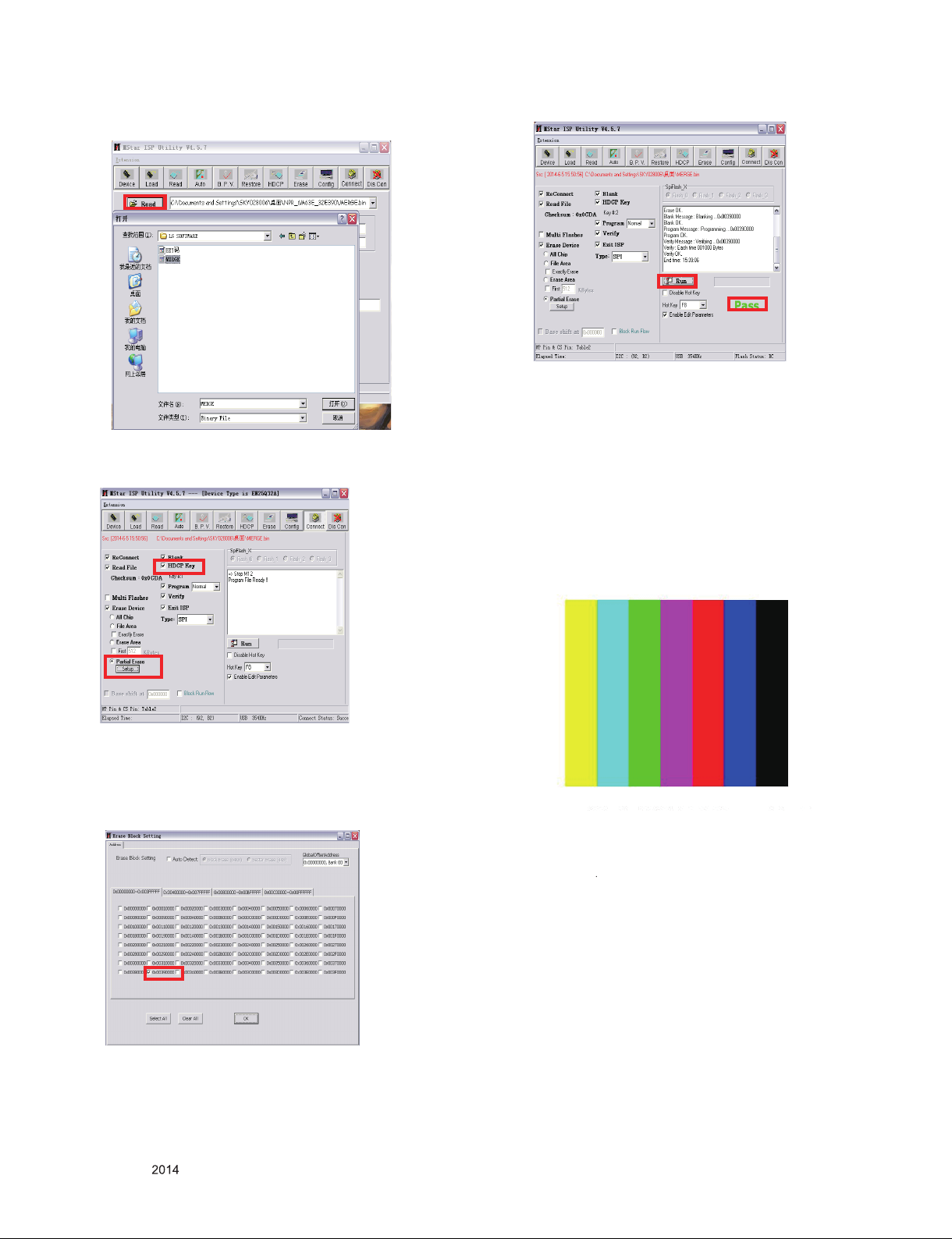
6. Click “Read” to load the main software for this TV set.
7. Click “Auto”to ready for HDCP Key updating. Settings
as below:
9. Click “Run” to update the HDCP Key.
Warm Tips:
The HDCP Key index value will be increased automatically.
That means after you update the first TV set, you only need
to connect another TV set to your PC, click “Connect”, then
“Run” to update.
4. ADC Process
4.1. ADC
- Set TV to YUV source by pushing"YUV)key
- Input full color bar signal using HD signal generator
Begin adjust by pushing “ADC ADJ" key
* Required equipment : Factory remote control.
HD signal generator.
EZ ADJUST
0
1. Tool Option2
2. Tool Option3
3. Tool Option4
4. Tool Option5
5. Tool Option Commercial
6. Country Group
7. Area Option
9. White Balance
10. 10 Point WB
11. Test Pattern
12. EDID D/L
13. Sub B/C
14. Ext. Input Adjust
ADC Calibration
ADC Comp 480i
ADC Comp 1080p
ADC Type
Reset
NG
NG
8. Click to select “Partial Erase”, then click Setup. An erase
block setting window will pop up. Choose the bank according
to "0X390000"for 32LB520B/60LB5200/65LB5200. Click
“OK”to confirm.
Only for training and service purposes
- 9 -
100% color bar
Note: 1. The YPBPR Auto White Balance adjust
(AUTO ADC) must be done on the product line.
2
In YPBPR channel ,must adjust the SD
and HD two modes.
4.2. Function Check
4.2.1. Check display and sound
■ Check Input and Signal items.
(1) TV
(2) AV (CVBS)
(3) COMPONENT (1080I/480i)
(4) HDMI
* Display and Sound check is executed by Remote control.
<Caution> Not to push the "RESTORE" key after
completion if the function inspection.
LGE Internal Use OnlyCopyright © LG Electronics. Inc. All rights reserved.
Page 10
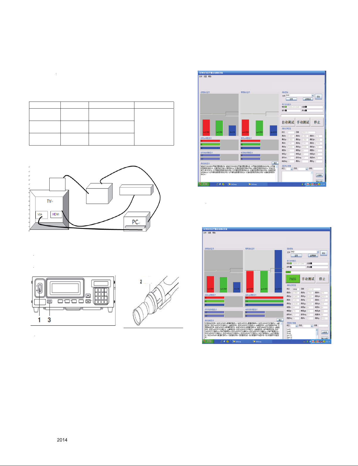
5. Total Assembly line process
5.1. Adjustment Preparation
▪ W/B Equipment condition
CA310
▪ evobA 5 minutes H/run in the inner pattern. ("power on" key
of Adjustment remote control)
* * The spec of color temperature and coordinate.
Mode Color Temp Color coordinate Remark
Cool (C50) 13,000 K
Medium(0) 9,300 K
Warm(W50) 6,500 K
Auto Adjust -W/B
CH01, Test signal: Inner pattern(80IRE)-LED Module
X=0.271 (±0.002)
Y=0.270 (±0.002)
X=0.286 (±0.002)
Y=0.289 (±0.002)
X=0.313 (±0.002)
Y=0.329 (±0.002)
Probe
Color
analyzer
<Test Signal>
- Inner pattern
for W/B adjust
- External white
pattern
(80IRE, 204gray)
HD signal generator
Click the "application "button and begin to adjust
5
automatically when finished ,it will display PASS.
*STEPS:
1
Connect Debug line.
2. Connect HDMI port and input 80% full white signal.
3
Calibrate the color analyzer (CA310).
Positioning
Ring
4
Open W/B auto adjust system and load saved parameters.
Only for training and service purposes
- 10 -
LGE Internal Use OnlyCopyright © LG Electronics. Inc. All rights reserved.
Page 11
* Manual W/B process using adjust Remote control.
■ Color analyzer(CA310,CA210)should be used in the
calibrated ch.
■ Operate the zero-calibration of the CA310 or CA210,
then stick sensor to the module when adjusting.
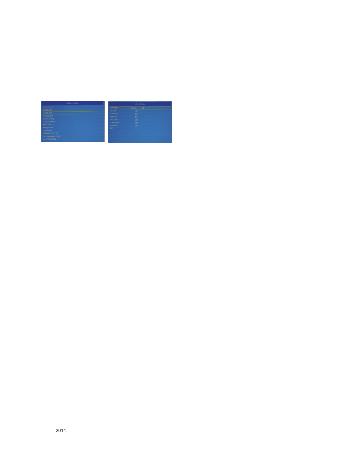
■ Enter factory mode by pushing customer remote controller:
input 3195.
■ Select W/B ADJUST item , push "ok" then enter into
adjust page.
■ For manual adjustment, it is also possible by the following
sequence.
(1) Set TV in aging mode by play a picture or music by USB for
more than 30 minutes. (if not executed this step the condition
for w/B will be different).
(2) Push “Exit” key.
(3) Enter factory mode by pushing customer remote controller:
input 3195. Select W/B ADJUST item , push "ok" then en
ter into adjust page.
(4) Zero Calibrate the probe of Color Analyzer, then place it
on the center of LCD module within 10cm of the surface
(5) Select each items (Red/Green/Blue Gain) using
▲/▼(CH +/-) key on Remote control.
(6) Adjust R/ G/ B Gain using ◄/►(VOL +/-) key on R/C.
(7) Adjust three modes all (Cool / Medium / Warm)
- For All model
Fix the one of R/G/B gain and change the others
- For G-FIX model
Cool Mode
1) Fix the one of R/G/B gain to 192 (default data) and
decrease the others. (If G gain is adjusted over 172
and R and B gain less than 192 , Adjust is O.K.)
2) If G gain is less than 172, Increase G gain by up to
172, and then increase R gain and G gain same
amount of increasing G gain.
3) If R gain or B gain is over 255, readjust G gain less
than 172, Conform to R gain is 255 or B gain is 255
Medium / Warm Mode - Fix the one of R/G/B gain
to 192 (default data) and decrease the others.
(8) When adjustment is completed, exit adjustment mode
using EXIT key on Remote control.
* CASE Cool
First adjust the coordinate far away from the target
value(x, y).
1) x, y > target
i) Decrease the R, G.
2) x, y < target
i) First decrease the B gain,
ii) Decrease the one of the others.
3) x > target, y < target
i) First decrease B, so make y a little more than the
target.
ii) Adjust x value by decreasing the R.
4) x < target, y > target
st decrease B, so make x a little more than the
i) Fir
target.
ii) Adjust x value by decreasing the G.
*
After You finish all adjustments and function inspections,
Press “SETTING” button , choose Initial Setting” option,
and choose “Yes”. It will show choose language picture,
then turn off TV and unplug the AC cable.
Only for training and service purposes
- 11 -
LGE Internal Use OnlyCopyright © LG Electronics. Inc. All rights reserved.
Page 12

5.4. Outgoing condition Configuration
■ When pressing RESTORE key by Service remote control,
Red LED are blinked alternatively. And then automatically
turn off. (Must not AC power OFF during blinking)
5.5. GND and HI-POT Test
5.5.1. GND & HI-POT auto-check preparation
(1) Check the POWER CABLE and SIGNAL CABE insertion
condition.
(2) You can’t use Tuner Ground & Tuner signal line at all
models (applied Isolator inner tuner)
5.5.2. GND & HI-POT auto-check
(1) Pallet moves in the station.(POWER CORD / AV CORD is
tightly inserted)
(2) Connect the AV JACK Tester.
(3) Controller on.
(4) GND Test (Auto)
- If Test is failed, Buzzer operates.
- If Test is passed, execute next process(Hi-pot test).
(Remove A/V CORD from A/V JACK BOX)
(5) HI-POT test (Auto)
- If Test is failed, Buzzer operates.
- If Test is passed, GOOD Lamp on and move to next
process automatically.
5.5.3. Checkpoint
(1) Test voltage
1) 3 Poles
- GND: 1.5 KV/min at 100 mA
- SIGNAL: 3 KV/min at 100 mA
2) 2 Poles
- SIGNAL: 3 KV/min at 100 mA
(2) TEST time: 1 second
(3) TEST POINT
1) 3 Poles
- GND Test = POWER CORD GND and SIGNAL
CABLE GND.
- Hi-pot Test = POWER CORD GND and LIVE &
NEUTRAL.
2) 2 Poles
- Hi-pot Test = Accessible Metal and LIVE & NEUTRAL.
(4) LEAKAGE CURRENT: At 0.5 mArms
Only for training and service purposes
- 12 -
LGE Internal Use OnlyCopyright © LG Electronics. Inc. All rights reserved.
Page 13
522
540
521
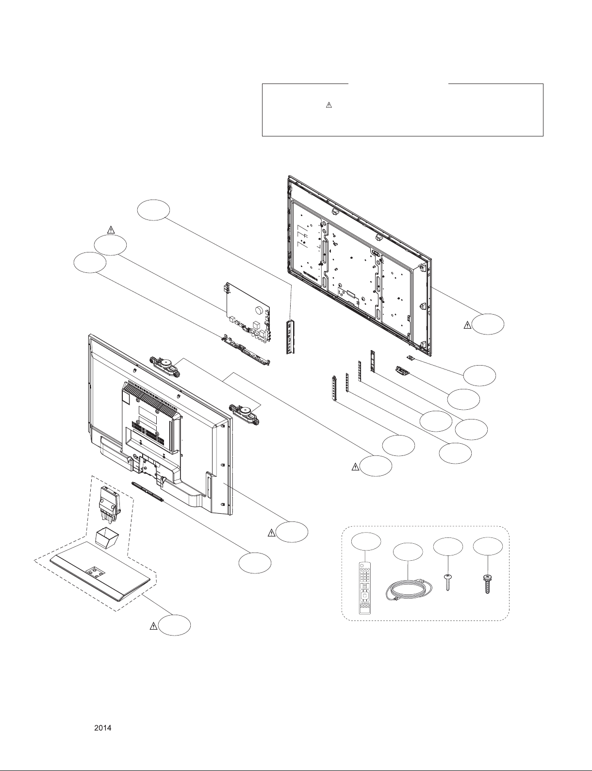
EXPLODED VIEW
IMPORTANT SAFETY NOTICE
Many electrical and mechanical parts in this chassis have special safety-related characteristics. These
parts are identified by in the Schematic Diagram and EXPLODED VIEW.
It is essenti al that these spec ial safety parts s hould be replace d with the same compone nts as
recommended in this manual to prevent X-RADIATION, Shock, Fire, or other Hazards.
Do not modify the original design without permission of manufacturer.
200
900
610
400
120
A2
511
A3
510
512
A9
500
600
513
A10
Only for training and service purposes
- 13 -
LGE Internal Use OnlyCopyright © LG Electronics. Inc. All rights reserved.
Page 14
SCHEMATIC CIRCUIT DIAGRAM
5
Connetor
D D
+12V_PWR
BL-ON/OFF
BL-ADJUST
+12V
BL-ON/OFF
BL-ADJUST
5V Standby Power(option) 3A
+12V_PWR
C2
C3
10uF/16V/0805
0.1uF/0402/16V
10uF/16V/0805
C4
20K/0402/5%
2.2nF/0402/16V
4
R1 100K/0402/5%
R3 27K/0402/5%
C5
1nF/0402/16V/NC
R7
0.1uF/0402/16V
C8
C6
U1
AOZ3015PI/SOP8
2
VIN
7
EN
6
COMP
4
VCC
3
2
Inverter controller
+5V_Standby
9
L1 22uH_3A
LX
8
Vo
5
FB
1
PGND
AGND
3
R1
R5 51K/0402/1%
C7
0.1uF/0402/16V/NC
R2
R10 9.1K/0402/1%
+
CA3
470uF/16V/EC3.5
C1
0.1uF/0402/16V
BL-ON/OFF
BL-ADJUST
R6
100R/0402/5%
R9
22K/0402/5%
+5V_Normal
R2
200R/0402/5%/NC
Q2
3904/SOT-23
2 3
R4
4.7K/0402/5%
Q1
3904/SOT-23
2 3
1
1
10K/0402/5%
R11
4.7K/0402/5%
R8
VBL_CTRL
BRI_ADJ
1
Vout=0.8V*(1+R1/R2)
C
Power Switch
STANDBY
STANDBY
B
STANDBY
STANDBY
R15
22K/0402/5%
R24
22K/0402/5%
+5V_Standby
R12
100K/0402/5%
1
Q3
3904/SOT-23
2 3
+12V_PWR
R21
100K/0402/5%
1
Q4
3904/SOT-23
2 3
0.1uF/0402/16V
R13
100K/0402/5%
0.1uF/0402/16V
R23
100K/0402/5%
C9
0.1uF/0402/16V/NC
U2
4953/SOP8
1
2
3
C10
4
C20
S1
G1
S2
G2
C11
0.1uF/0402/16V/NC
8
+5V_Normal
D1
7
D1
6
+12V_NORMAL
D2
5
D2
Standby controller
+3.3V_Normal
STANDBY
STANDBY
R19
200R/0402/5%
H :Power on
L :Power off
R16
4.7K/0402/5%
PWR-ON/OFF
If POWER BOARD IS 5stb ONLY ,PL NOT PATCH THESE GUY.
1.5V/1.8V Power_Normal
4
U4
ADJ
OUT
AMS1117-Adj
IN
C22
2.2uF/0603/16V
0.1uF/0402/16V
CA9
+
200uF/35V/ECS-5M
321
0.1uF/0402/16V
C24
C23
2.2uF/0603/16V
+1.8V_DDR2
C25
R1
220R/0402/5%/470R/0402/5%
R26
+5V_Normal
R2
R27
100R/0402/5%
A A
3.3V Power
4
ADJ
OUT
+5V_Standby
C26
2.2uF/0603/16V
0.1uF/0402/16V
IN
321
C27
U5
AMS1117-3.3
+3.3V_Normal
C28
2.2uF/0603/16V
+3.3V_Normal
C29
0.1uF/0402/16V
Test Point & MARK
H1
1
5
4
3
2
NC
1
1
H5
NC
NC
H2
9
8
7
6
H6
1
5
9
4
8
3
7
2
6
NC
1
H7
NC
H3
1
5
4
3
2
NC
H4
1
5
9
4
8
3
7
2
6
NC
1.15V Core Power
+12V_PWR
C17
10uF/16V/0805
C18
10uF/16V/0805
Vout=0.8V*(1+R1/R2)
NOTICE:
9
8
7
6
R17
10K/0402/5%
3
5
1
U3
MP1470
IN
EN
GND
R14
6
BST
20R/0402/5%
C12
2
SW
4
FB
C21
10pF/0402/16V
If chip is 3393,The R2 Value is 10K 1%
If chip is 6306,The R2 Value is 8.2K 1%
1uF/0402/16V
L2
22uH_3A
R18
4.7K/0402/1%
R1
R20
100K/0402/5%
Resistors close to the DC-DC
R22
10K/0402/1% or 8.2K/0402/1%
R2
C13
10uF/16V/0805
R25
470R/0402/5%
Max :1.0A
VDDC
0.1uF/0402/16V
C19
C14
10uF/16V/0805
10uF/16V/0805
C15
10uF/16V/0805
C16
100uF/35V/ECS-5M
+
CA8
Vout=1.25V*(R1+R2)/R1
C
B
NOTICE:
If chip is 3393,The R1 Value is 220R 5% Vout=1.8V
If chip is 6306,The R1 Value is 470R 5% Vout=1.5V
5
4
Title
Title
Title
Custom
Custom
3
2
Custom
MSD3393
MSD3393
MSD3393
System power
System power
System power
1
veRrebmuN tnemucoDeziS
veRrebmuN tnemucoDeziS
veRrebmuN tnemucoDeziS
1.0
1.0
teehS:etaD
1 9Friday, September 27, 2013
1 9Friday, September 27, 2013
1 9Friday, September 27, 2013
teehS:etaD
teehS:etaD
1.0
of
of
of
Page 15
5
HDMI Interface
HDMI0-RX0P
HDMI0-RX0N
HDMI0-RX1P
HDMI0-RX1N
HDMI0-RX2P
HDMI0-RX2N
HDMI0-CLKN
HDMI0-CLKP
HDMI0-SCL
HDMI0-SDA
HDMI0-HPDIN
HDMI1-RX0P
HDMI1-RX0N
HDMI1-RX1P
D D
HDMI1-RX1N
HDMI1-RX2P
HDMI1-RX2N
HDMI1-CLKN
HDMI1-CLKP
HDMI1-SCL
HDMI1-SDA
HDMI1-HPDIN
HDMI2-RX0P
HDMI2-RX0N
HDMI2-RX1P
HDMI2-RX1N
HDMI2-RX2P
HDMI2-RX2N
HDMI2-CLKN
HDMI2-CLKP
HDMI2-SCL
HDMI2-SDA
HDMI2-HPDIN
MHL_CABLE-DET
HDMI-ARC
HDMI-CEC
PC & YPBPR Interface
VGA-Rin
VGA-Gin
VGA-Bin
VGA_HSYNC
VGA_VSYNC
C C
YPbPr_PR
YPbPr_Y
YPbPr_PB
CVBS IN & OUT
AV1
CVBS1_OUT
HDMI0-RX0P
HDMI0-RX0N
HDMI0-RX1P
HDMI0-RX1N
HDMI0-RX2P
HDMI0-RX2N
HDMI0-CLKN
HDMI0-CLKP
HDMI0-SCL
HDMI0-SDA
HDMI0-HPDIN
HDMI1-RX0P
HDMI1-RX0N
HDMI1-RX1P
HDMI1-RX1N
HDMI1-RX2P
HDMI1-RX2N
HDMI1-CLKN
HDMI1-CLKP
HDMI1-SCL
HDMI1-SDA
HDMI1-HPDIN
HDMI2-RX0P
HDMI2-RX0N
HDMI2-RX1P
HDMI2-RX1N
HDMI2-RX2P
HDMI2-RX2N
HDMI2-CLKN
HDMI2-CLKP
HDMI2-SCL
HDMI2-SDA
HDMI2-HPDIN
MHL_CABLE-DET
HDMI-ARC
HDMI-CEC
R28 33R/0402/5%
R29 68R/0402/5%
R30 33R/0402/5%
R31 33R/0402/5%
R32 33R/0402/5%
R33 68R/0402/5%
R34 33R/0402/5%
R35 33R/0402/5%
R36 0R/0402/5%
R38 150R/0402/5%
R39 180R/0402/5%
C48 47nF/0402/16V
C49 47nF/0402/16V
C50 47nF/0402/16V
C51 47nF/0402/16V
VGA_HSYNC
VGA_VSYNC
C52 47nF/0402/16V
C53 47nF/0402/16V
C54 47nF/0402/16V
C55 47nF/0402/16V
C56 1nF/0402/16V
C58 47nF/0402/16V
C60 47nF/0402/16V
RGB0_R+
RGB0_GRGB0_G+
RGB0_B+
RGB1_R+
RGB1_GRGB1_G+
RGB1_B+
RGB1_SOG
CVBS0+
CVBS_VCOM
CVBS1_OUT
HDMI2-RX1N
HDMI2-RX1P
HDMI2-RX2N
HDMI2-RX2P
+3.3V_Normal
HDMI1-CLKN
HDMI1-CLKP
HDMI1-RX0N
HDMI1-RX0P
HDMI1-RX1N
HDMI1-RX1P
HDMI1-RX2N
HDMI1-RX2P
VGA_HSYNC
RGB0_B+
RGB0_G+
RGB0_GRGB0_R+
VGA_VSYNC
+3.3V_Normal
RGB1_B+
RGB1_SOG
RGB1_G+
RGB1_GRGB1_R+
CVBS0+
CVBS_VCOM
CVBS1_OUT
LINEIN_R1
LINEIN_L1
AU_VAG
AU_VRM
VDDC
+3.3V_AU
AUDIO IN
VGA-Lin_AU
VGA-Rin_AU
AV1-Lin
AV1-Rin
VGA-Lin_AU
VGA-Rin_AU
AV1-Lin
AV1-Rin
C61 2.2uF/0603/16V
C63 2.2uF/0603/16V
C64 2.2uF/0603/16V
C65 2.2uF/0603/16V
LINEIN_L1
LINEIN_R1
LINEIN_L4
LINEIN_R4
DIF IN
VIFP
IFP
IFN
B B
USB & SPDIF_OUT
USB2_DUSB2_D+
USB1_DUSB1_D+
SPDIF_OUT
C67
0.1uF/0402/16V
VIFM
C68
0.1uF/0402/16V
USB2_DUSB2_D+
USB1_DUSB1_D+
SPDIF_OUT
C69
2.2uF/0603/16V
L6
AU_VRM
AU_VAG
C70
0.1uF/0402/16V
2.2uF/0603/16V
C71
RESET
+5V_Standby
DEBUG
A A
MUST pull high to 5VSTB
ISP AND VGA EDID
R49
100K/0402/5%
R50
10K/0402/5%
C78
2.2uF/0603/16V
UART-TX
R66 100R/0402/5%
UART-RX
R67 100R/0402/5%
3
D1
BAV99
C75
1
2
2.2uF/0603/16V
1
Q5
3906/SOT-23
R52
3 2
R54
100K/0402/5%
+5V_Standby
R64
4.7K/0402/5%
1K/0402/5%
R65
4.7K/0402/5%
5
System-RST
C77
1nF/0402/16V
UART_TX
UART_RX
0R/0603/5%
XTAL
R51
XTALO
0R/0402/5%
XTALI
FLASH
+3.3V_Normal
SPI_SCK
SPI_SDI
C81
0.1uF/0402/16V
R53
1M/0402/5%
Y1
24MHz
3
U7
MX25L3205
8
VDD
7
HOLD#
6
SCK
5
SI
C76
33pF/0402/16V
C79
33pF/0402/16V
WP#
4
TP4
HDMI2-RX0N
HDMI2-RX0P
1
131
127
128
132
129
130
U6
Test
MARK
MARK
E-PAD
RX0P_B
RX0N_B
1
RX1N_B
2
RX1P_B
3
RX2N_B
4
RX2P_B
5
AVDD_MOD
6
RXCN_A
7
RXCP_A
8
RX0N_A
9
RX0P_A
10
RX1N_A
11
RX1P_A
12
RX2N_A
13
RX2P_A
14
HSYNC0
15
BIN0P
16
GIN0P
17
GIN0M
18
RIN0P
19
VSYNC0
20
AVDD3P3_ADC
21
BIN1P
22
SOGIN1
23
GIN1P
24
GIN1M
25
RIN1P
26
VSYNC1
27
CVBS1
28
CVBS0
29
VCOM
30
CVBS_OUT1
31
VDDC
32
AVDD_AU33
33
AUR0
34
AUL0
35
AUR1
36
AUL1
37
VAG
38
VRM
AUR440AUOUTL3
AUL4
MSD3393LU
39
LINEIN_L4
LINEIN_R4
+3.3V_TU
Close to Mstar IC
R43
10K/0402/5%
IFAGC
R46
0R/0402/5%
CHIP_CONFIG
{IPAD_PWM1, PAD_PWM0}
B51_NO_EJ
PWM1
R57 4.7K/0402/5%
PWM0
R58 4.7K/0402/5%
+3.3V_Normal
1
SPI_CSN
CE#
2
SPI_SDO
SO
3
#F_WP
4
VSS
4
VDDC
HDMI2-CLKN
HDMI2-CLKP
HDMI0-RX1P
HDMI0-RX2N
HDMI0-RX2P
125
126
123
124
122
RX2P_D
RX1P_D
RX2N_D
RXCP_B
RXCN_B
AVDD5V_MHL
HDMI2-SCL
HDMI0-RX0P
120
RX1N_D
HDMI2-HPDIN
HDMI0-RX0N
HDMI0-CLKN
HDMI0-CLKP
116
117
118
119
112
115
113
114
RX0P_D
RX0N_D
RXCP_D
RXCN_D
AVDD_5V
HOTPLUG_B
GND_EFUSE
VDDC/AVDDL_DVI
HDMI0-RX1N
121
MSD3393LU
48
+3.3V_ADC
IFAGC-T
VDDC/DVDD_DDR_CMD54VDDIO_CMD
AVDD_MOD
AVDD3P3_DADC
55
53
51
52
+1.8V_DDR2
+3.3V_PLL
+3.3V_Normal
VDDC
XTALO
XTALI
TUNER_SDA
AUOUTL043AUOUTR3
41
42
LINE3OUT_L
LINE3OUT_R
LINE0OUT_L
LINE0OUT_R
C72
22nF/0402/16V
4'h00
R63
10K/0402/5%
VIFP46VIFM47AUOUTR044IFAGC45XIN50AVDD3P3_DMPLL49Xout
VIFM
VIFP
IFAGC
MHL_CABLE-DET
HDMI2-SDA
111
110
DDCDB_CL
DDCDB_DA
GPIO0/GPIO44
GPIO1/GPIO45
57
56
TUNER_SCL
MHL_VBUS-EN
HDMI1-SDA
109
MHL_DET
AMP-MUTE
HDMI1-SCL
HDMI0-SDA
107
108
DDCDA_CL
DDCDA_DA
DDCDC_DA
GPIO3/GPIO4758GPIO4/GPIO4859LVA3P61GPIO2/GPIO46
GPIO5/GPIO49
60
PWR-ON/OFF
SPDIF_OUT
VDDC
+1.8V_DDR2
ARC_DET
HDMI0-SCL
105
103
106
104
DDCDC_CL
VDDIO_DATA
VDDC/DVDD_DDR_DATA
HOTPLUG_C/D
LVA3M62LVACKP
64
63
R70
22R/0402/5%
B3_RXE3-
B2_RXE3+
B4_RXEC+
B5_RXEC-
PWR-ON/OFF
MHL_VBUS-EN
PANEL_ON/OFF
SAR2
SAR1
SAR0
AVDD_MOD
DP_P1
DM_P1
DP_P0
DM_P0
RESET
INT/GPIO64
TEST
DDCA_CK
DDCA_DA
SPI_CK
SPI_CZ
SPI_DI
SPI_DO
PWM0
PWM1
HOTPLUG_A
LDE/LVB0M
LCK/LVB0P
LVB1M
LVB1P
LVB2M
LVB2P
AVDD_MOD
LVB3M
LVB3P
LVA0M
LVA0P
LVA1M
LVA1P
LVA2M
LVA2P
LVACKM
R72
22R/0402/5%
IR-in
KEY0-SAR0
KEY1-SAR1
BRI_ADJ
VBL_CTRL
AMP-MUTE
ARC_DET
TUNER_SCL
TUNER_SDA
IRIN
CEC
ARC
102
101
100
99
98
97
96
95
94
93
92
91
90
89
88
87
86
85
84
83
82
81
80
79
78
77
76
75
74
73
72
71
70
69
68
67
66
65
FOR EMI
R7_RXO0R6_RXO0+
R5_RXO1R4_RXO1+
R3_RXO2R2_RXO2+
G7_RXO3G6_RXO3+
G3_RXE0G2_RXE0+
G1_RXE1G0_RXE1+
B7_RXE2B6_RXE2+
B5_RXECB4_RXEC+
B3_RXE3B2_RXE3+
3
KEY1-SAR1
KEY0-SAR0
+3.3V_Normal
USB2_D+
USB2_DUSB1_D+
USB1_DSystem-RST
PANEL_ON/OFF
IR-in
HDMI-CEC
UART-RX
UART-TX
HDMI-ARC
SPI_SCK
SPI_CSN
SPI_SDI
SPI_SDO
BRI_ADJ
VBL_CTRL
HDMI1-HPDIN
HDMI0-HPDIN
R7_RXO0R6_RXO0+
R5_RXO1R4_RXO1+
R3_RXO2R2_RXO2+
+3.3V_Normal
G7_RXO3G6_RXO3+
G3_RXE0G2_RXE0+
G1_RXE1G0_RXE1+
B7_RXE2B6_RXE2+
PWR-ON/OFF
PWM0
PWM1
MHL_VBUS-EN
AMP-MUTE
PANEL_ON/OFF
ARC_DET
TUNER_SCL
TUNER_SDA
R7_RXO0R6_RXO0+
R5_RXO1R4_RXO1+
R3_RXO2R2_RXO2+
G7_RXO3G6_RXO3+
G3_RXE0G2_RXE0+
G1_RXE1G0_RXE1+
B7_RXE2B6_RXE2+
B5_RXECB4_RXEC+
B3_RXE3B2_RXE3+
3
VDDC 1.15V
VDDC
C30
2.2uF/0603/16V
DDR2 1.8V
+1.8V_DDR2
C35
2.2uF/0603/16V
3.3V
+3.3V_Normal
C40
2.2uF/0603/16V
C31
0.1uF/0402/16V
C36
0.1uF/0402/16V
C41
0.1uF/0402/16V
0.1uF/0402/16V
C32
0.1uF/0402/16V
3.3V audio
+3.3V_Normal
C38
0.1uF/0402/16V
C42
0.1uF/0402/16V
C33
0.1uF/0402/16V
L3
0R/0603/5%
0.1uF/0402/16V
C43
Audio Line Out
LINE0OUT_L
LINE0OUT_R
LINE3OUT_L
LINE3OUT_R
Close to Mstar IC
IR&KEYB
J1
CON20W-J20-12
IR_in
1nF/0402/16V
1nF/0402/16V
1nF/0402/16V
1nF/0402/16V
1
2
3
4
5
6
7
8
9
10
11
12
+5V_Standby
R60
10K/0402/5%
R62
1K/0402/5%
C165
C57
C62
C66
+5V_Standby
KEY0-in
KEY1-in
IR_in
LED_G
LED_R
R37
200K/0402/5%
R40
200K/0402/5%
R41
200K/0402/5%
R42
200K/0402/5%
+3.3V_Normal
IR-in
C80
33pF/0402/16V
D13
ESD
2
C34
0.1uF/0402/16V
1
3.3V MPLL
+3.3V_Normal
+3.3V_AU
C37
0.1uF/0402/16V
L5
0R/0603/5%
C44
C45
0.1uF/0402/16V
AV_AUOUTL1
AV_AUOUTR1
LINEOUT_APML
LINEOUT_APMR
+3.3V_Normal
R44
8.2K/0402/5%
KEY0-in KEY0-SAR0
C74
0.1uF/0402/16V
D12
ESD
STANDBY
L4
0R/0603/5%
+3.3V_ADC
C46
2.2uF/0603/16V
R47
1K/0402/5%
R61
22K/0402/5%
+3.3V_PLL
C39
0.1uF/0402/16V
C47
0.1uF/0402/16V
+3.3V_Normal
Q7
1
3904/SOT-23
2 3
KEY1-in
R55
2K/0402/5%
LED_G
+3.3V_Normal
R45
8.2K/0402/5%
R59
4.7K/0402/5%
R48
1K/0402/5%
C73
0.1uF/0402/16V
+3.3V_Normal
Q6
1
3904/SOT-23
R56
2K/0402/5%
LED_R
2 3
KEY1-SAR1
Standby :L :Power on Green Led
H :Power off Red Led
Title
Title
Title
Size Document Number Rev
Size Document Number Rev
Size Document Number Rev
C
C
C
Date: Sheet
Date: Sheet
2
Date: Sheet
MSD3393
MSD3393
MSD3393
MAIN CHIP
MAIN CHIP
MAIN CHIP
1
1.0
1.0
29Wednesday, June 11, 2014
29Wednesday, June 11, 2014
29Wednesday, June 11, 2014
1.0
of
of
of
Page 16
5
4
LVDS CONNECTOR ( 1 DIP + 2 SMT OPTIONAL )
3
2
1
HI CONNECTOR
D D
CN2
DIP/20*2
R7_RXO0R5_RXO1R3_RXO2R1_RXOCG7_RXO3-
G3_RXE0G1_RXE1B7_RXE2-
C C
B5_RXECB3_RXE3-
VCC-Panel
C85
0.1uF/0402/16V
40
A0-
38
A1-
36
A2-
34
AC-
32
A3-
30
A4-
28
GND
26
DCR-I
24
MODE
22
SG
20
B0-
18
B1-
16
B2-
14
BC-
12
B3-
10
B4-
8
GND
6
GND
4
VCC
2
VCC
A0+
A1+
A2+
ACA3+
A4+
GND
DCR-O
GND
B0+
B1+
B2+
BC+
B3+
B4+
GND
GND
VCC
VCC
39
37
35
33
31
29
27
25
23
I/O
21
19
17
15
13
11
9
7
5
3
1
R6_RXO0+
R4_RXO1+
R2_RXO2+
R0_RXOC+
G6_RXO3+
G2_RXE0+
G0_RXE1+
B6_RXE2+
B4_RXEC+
B2_RXE3+
Power for panel
+5V_Normal
+12V_NORMAL
PANEL_ON/OFF
Net to other page
R7_RXO0R6_RXO0+
R5_RXO1R4_RXO1+
R3_RXO2R2_RXO2+
G7_RXO3G6_RXO3+
FB3 0R/1206/5%/NC
FB4 0R/1206/5%
PANEL_ON/OFF
R7_RXO0R6_RXO0+
R5_RXO1R4_RXO1+
R3_RXO2R2_RXO2+
G7_RXO3G6_RXO3+
0.1uF/0402/16V/NC
R71
4.7K/0402/5%
R73
10K/0402/5%
G3_RXE0G2_RXE0+
G1_RXE1G0_RXE1+
B7_RXE2B6_RXE2+
B5_RXECB4_RXEC+
B3_RXE3B2_RXE3+
R1_RXOC- B5_RXECR0_RXOC+ B4_RXEC+
VPANEL_IN
C82
100K/0402/5%
1
3904/SOT-23
G3_RXE0G2_RXE0+
G1_RXE1G0_RXE1+
B7_RXE2B6_RXE2+
B5_RXECB4_RXEC+
B3_RXE3B2_RXE3+
R68
100K/0402/5%
Q9
2 3
C83
1uF/0402/16V/NC
R69
U8 9435/SOP8
1
S
2
3
4
AO3401A/SOT-23/NC
D
S
D
S
D
G
D
Q8
C84
0.1uF/0402/16V/NC
5
6
7
8
470uF/16V/EC3.5
VCC-Panel
CA11
+
B B
A A
Title
Title
Title
Size Document Number Rev
Size Document Number Rev
Size Document Number Rev
B
B
B
Date: Sheet
Date: Sheet
5
4
3
2
Date: Sheet
MSD3393
MSD3393
MSD3393
LVDS Interface
LVDS Interface
LVDS Interface
1.0
1.0
1.0
of
of
of
39Wednesday, June 11, 2014
39Wednesday, June 11, 2014
39Wednesday, June 11, 2014
1
Page 17
5
D D
4
3
2
1
AUDIO IN
P1
WHITE
1
C C
RED
RCA-2P
HD_L
2
3
4
HD_R
HD_L
HD_R
220pF/0402/16V/NC
C87
C86
220pF/0402/16V/NC
R76 10K/0402/5%
R77 10K/0402/5%
R79
12K/0402/5%
AV1-Lin
AV1-Rin
R80
12K/0402/5%
YPBPR & AV IN
B B
P2
YPbPr_PR
YPbPr_PB
AV1
YPbPr_Y
RCA-3P
12
34
56
D14
ESD
AV1-IN
R85
75R/0402/5%
R84
75R/0402/5%
75R/0402/5%
Close to Mstar IC
R83
R199
0R/0402/5%
VIDEO OUT
SPDIF OUT
R81
330R/0402/5%
SPDIF_O
R82
100R/0402/5%
P14
3
INPUT
2
VCC
1
GND
NC/FIBER-OPTIC
1
TP2
Closed to IC
+5V_Normal
NC/C88
0.1uF/0402/16V/NC
CVBS1_OUT
FOR ATV/AV DEBUG
SPDIF_OUT
C102
33pF/0402/16V
SPDIF_O
NC/RV1
ESD
A A
Title
Title
Title
Size Document Number Rev
Size Document Number Rev
Size Document Number Rev
B
B
B
Date: Sheet
Date: Sheet
5
4
3
2
Date: Sheet
MSD3393
MSD3393
MSD3393
Video Interface
Video Interface
Video Interface
1.0
1.0
1.0
of
of
of
49Monday, July 14, 2014
49Monday, July 14, 2014
49Monday, July 14, 2014
1
Page 18
5
4
3
2
1
VGA
P4
D D
C C
R92
10K/0402/5%
1617
11
12
13
14
15
VGA/15 PIN
R93
10K/0402/5%
1
6
2
7
3
8
4
9
5
10
DDC_SCL_D
DDC_SDA_D
R90100R/0402/5%
R91100R/0402/5%
VGA-Rin
VGA-Gin
VGA-Bin
UART_RX
UART_TX
VGA_VSYNC
VGA_HSYNC
VGA AUDIO IN
P5
PHONEJACK
1
2
5
3
4
R86 10K/0402/5%
R87 10K/0402/5%
R88
12K/0402/5%
R89
12K/0402/5%
VGA-Lin_AU
VGA-Rin_AU
C89
220p/0402/16V
VGA-Lin_AU
VGA-Rin_AU
C90
220p/0402/16V
B B
VGA-Bin
VGA-Gin
VGA-Rin
R94
75R/0402/5%
R95
R96
75R/0402/5%
75R/0402/5%
VGA-Bin
VGA-Gin
VGA-Rin
Close to Mstar IC
A A
Title
Title
Title
MSD3393
MSD3393
MSD3393
Size Document Number Rev
Size Document Number Rev
Size Document Number Rev
A
A
A
Date: Sheet
Date: Sheet
5
4
3
Date: Sheet
VGA Interface
VGA Interface
VGA Interface
2
of
of
of
59Wednesday, May 14, 2014
59Wednesday, May 14, 2014
59Wednesday, May 14, 2014
1
1.0
1.0
1.0
Page 19
5
4
3
2
1
USB INTERFACE
D
C C
5
6
5
6
P6
USB_A
5
6
5
6
1
1
2
3
4
P7USB_A
1
2
3
4
USB1_D1-_in
USB1_D1+_in
USB2_D1-_in
USB2_D1+_in
2
3
4
1
2
3
4
+5V_USB0
+5V_USB0
R97 2.2/0402/5%
R98 2.2/0402/5%
R99 2.2R
R100 2.2R
USB2_D-
USB2_D+
USB1_DUSB1_D+
USB2_D+
USB1_DUSB1_D+
USB2_D-
USB POWER
D2
+5V_USB0
C91
0.1uF/0402/16V
CA10
+
200uF/35V/ECS-5M
C93
0.1uF/0402/16V
+5V_Normal5V_USB
5V_USB
C92
2.2uF/0603/16V
5V_USB+5V_USB0
C94
2.2uF/0603/16V
D
B
A
Title
Title
Title
MSD3393
MSD3393
MSD3393
USB Interface
USB Interface
A
A
A
5
4
3
USB Interface
2
teehS:etaD
teehS:etaD
teehS:etaD
of
of
of
6 9Monday, July 14, 2014
6 9Monday, July 14, 2014
6 9Monday, July 14, 2014
1
veRrebmuN tnemucoDeziS
veRrebmuN tnemucoDeziS
veRrebmuN tnemucoDeziS
1.0
1.0
1.0
B
A
Page 20

5
P8
20
GND
21
GND
22
GND
23
GND
18
+5V
17
CEC/DDC GND
15
DDC SCL
16
DDC SDA
13
CEC
19
HPD
2
Dat2 shield
5
Dat1 shield
8
Dat0 shield
11
clk shield
D D
7
DAT0+
9
DAT0-
4
DAT1+
6
DAT1-
1
DAT2+
3
DAT2-
10
clk+
12
clk-
14
ARC1
HDMI
P9
20
GND
21
GND
22
GND
23
GND
18
+5V
17
CEC/DDC GND
15
DDC SCL
16
DDC SDA
13
CEC
19
HPD
2
Dat2 shield
5
Dat1 shield
8
Dat0 shield
11
clk shield
7
DAT0+
9
DAT0-
4
DAT1+
6
DAT1-
1
DAT2+
3
DAT2-
10
clk+
12
clk-
C C
14
ARC1
HDMI
P10
20
GND
21
GND
22
GND
23
GND
18
+5V
17
CEC/DDC GND
15
DDC SCL
16
DDC SDA
13
CEC
19
HPD
2
Dat2 shield
5
Dat1 shield
8
Dat0 shield
11
clk shield
7
DAT0+
9
DAT0-
4
DAT1+
6
DAT1-
1
DAT2+
3
DAT2-
10
clk+
12
clk-
14
ARC1
B
HDMI
HDMI3_RX0P
HDMI3_RX0N
HDMI3_RX1P
HDMI3_RX1N
HDMI3_RX2P
HDMI3_RX2N
HDMI3_CLKP
HDMI3_CLKN
HDMI3/5V
HDMI_ARC
HDMI3-DDC-SCL
HDMI3-DDC-SDA
CEC
HDMI3-HPD
HDMI1/5V
HDMI1-DDC-SCL
HDMI1-DDC-SDA
CEC
HDMI1-HPD
HDMI1_RX0P
HDMI1_RX0N
HDMI1_RX1P
HDMI1_RX1N
HDMI1_RX2P
HDMI1_RX2N
HDMI1_CLKP
HDMI1_CLKN
HDMI2-DDC-SCL
HDMI2-DDC-SDA
CEC
HDMI2-HPD
MHL_CD_SENSE
HDMI2_RX0P
HDMI2_RX0N
HDMI2_RX1P
HDMI2_RX1N
HDMI2_RX2P
HDMI2_RX2N
HDMI2_CLKP
HDMI2_CLKN
HDMI2/5V
HDMI3_RX2P
HDMI3_RX2N
HDMI3_RX1P
HDMI3_RX1N
HDMI3_RX0P
HDMI3_RX0N
HDMI3_CLKP
HDMI3_CLKN
HDMI1_RX2P
HDMI1_RX2N
HDMI1_RX1P
HDMI1_RX1N
HDMI1_RX0P
HDMI1_RX0N
HDMI1_CLKP
HDMI1_CLKN
R101 5.1R/0402/5%
HDMI3-RX2P
HDMI3-RX2N
R103 5.1R/0402/5%
HDMI3-RX1P
R107 5.1R/0402/5%
R108 5.1R/0402/5%
HDMI3-RX1N
HDMI3-RX0P
R109 5.1R/0402/5%
HDMI3-RX0N
R111 5.1R/0402/5%
HDMI3-CLKP
R113 5.1R/0402/5%
HDMI3-CLKN
R115 5.1R/0402/5%
R116 5.1R/0402/5%
R117 5.1R/0402/5%
R119 5.1R/0402/5%
R121 5.1R/0402/5%
R123 5.1R/0402/5%
R125 5.1R/0402/5%
R126 5.1R/0402/5%
R130 5.1R/0402/5%
HDMI2_RX2P
HDMI2_RX2N
HDMI2_RX1P
HDMI2_RX1N
HDMI2_RX0P
HDMI2_RX0N
HDMI2_CLKP
HDMI2_CLKN
HDMI1-RX2P
HDMI1-RX2N
HDMI1-RX1P
HDMI1-RX1N
HDMI1-RX0P
HDMI1-RX0N
HDMI1-CLKP
HDMI1-CLKN
R131 5.1R/0402/5%
HDMI2-RX2P
HDMI2-RX2N
R132 5.1R/0402/5%
HDMI2-RX1P
R133 5.1R/0402/5%
HDMI2-RX1N
R134 5.1R/0402/5%
HDMI2-RX0P
R137 5.1R/0402/5%
HDMI2-RX0N
R139 5.1R/0402/5%
R141 5.1R/0402/5%
HDMI2-CLKP
HDMI2-CLKN
R143 5.1R/0402/5%
HDMI0-RX2P
HDMI0-RX2N
HDMI0-RX1P
HDMI0-RX1N
HDMI0-RX0P
HDMI0-RX0N
HDMI0-CLKP
HDMI0-CLKN
HDMI1-RX2P
HDMI1-RX2N
HDMI1-RX1P
HDMI1-RX1N
HDMI1-RX0P
HDMI1-RX0N
HDMI1-CLKP
HDMI1-CLKN
HDMI3-DDC-SCL
HDMI3-DDC-SDA
HDMI2-RX2P
HDMI2-RX2N
HDMI2-RX1P
HDMI2-RX1N
HDMI2-RX0P
HDMI2-RX0N
HDMI2-CLKP
HDMI2-CLKN
10K/0402/5%
HDMI1-DDC-SCL
HDMI1-DDC-SDA
HDMI3/5V
R104
10K/0402/5%
10K/0402/5%
HDMI2-DDC-SCL
HDMI2-DDC-SDA
R105
R110 33R/0402/5%
R112 33R/0402/5%
HDMI1/5V
R124
R122
10K/0402/5%
AVDD5V_CD
47K/0402/5%
4
HDMI0-SCL
HDMI0-SDA
R127INS163289633R/0402/5%
R129 33R/0402/5%
R136
R135
10K/0402/5%
R140 33R/0402/5%
R142 33R/0402/5%
HDMI1-SCL
HDMI1-SDA
HDMI3-HPD
HDMI2-SCL
HDMI2-SDA
HDMI3/5V
HDMI1-HPD
R102
1K/0402/5%
Q10
1
R114 4.7K/0402/5%
3904/SOT-23
2 3
HDMI1/5V
R118
1K/0402/5%
3904/SOT-23
2 3
Q11
1
R128 4.7K/0402/5%
HDMI2-HPD
R106
10K/0402/5%
HDMI0-HPDIN
R120
10K/0402/5%
HDMI0-HPDIN
HDMI1-HPDIN
R138 33R/0402/5%
HDMI1-HPDIN
HDMI2-HPDIN
HDMI2-HPDIN
3
2
1
HDMI3
HDMI1
CEC & ARC MHL
HDMI_ARC HDMI-ARC
CEC
HDMI3/5V
C95
2.2uF/0603/16V
R144 200R/0402/5%
R148 4.7K/0402/5%
HDMI-CEC
R150
10K/0402/5%
HDMI-ARC
HDMI-CEC
ARC_DET
HDMI2/5V
+5V_Standby
R145 0R/0402/5%
D3
2
1
AVDD5V_CD
3
BAT54C/SOT23/NC
HDMI2/5V
R152 10R/0402/5%
AVDD5V_MHL
MHL_CD_SENSE
C96
47nF/0402/16V
R146 100R/0402/5%
R149
300K/0402/5%
MHL_CABLE-DET
MHL_CABLE-DET
MHL_VBUS-EN
R155
NC/1K/0402/5%
R154
100/0402/5%
+5V_Standby
R151
10K/0402/5%
R147 10K/0402/5%/NC
QA1
5
4
/EN
GND
AP2181DWG-7
HDMI2/5V
/OC3VIN
1
VOUT
2
B
HDMI2 With MHL
A A
Title
Title
Title
D
D
5
4
3
2
D
1
MSD3393
MSD3393
MSD3393
HDMI Interface
HDMI Interface
HDMI Interface
teehS:etaD
teehS:etaD
teehS:etaD
7 9Wednesday, June 11, 2014
7 9Wednesday, June 11, 2014
7 9Wednesday, June 11, 2014
of
of
of
veRrebmuN tnemucoDeziS
veRrebmuN tnemucoDeziS
veRrebmuN tnemucoDeziS
1.0
1.0
1.0
Page 21

Silicon TUNER
5
P12
1
234
CON3
234
3
4
5
6
7
16
17
18
19
5
P13
1
5
RCA1_6
D D
C C
120pF/0402/50V/NC
1
2
47nF/0402/16V/NC
C100
D11
ESD
+3.3V_TU
C98
1
2
3
C101
120pF/0402/50V
+3.3V_TU
C166
1nF/0402/16V
12
11
C1
VDD
GND
RF1
GND
GND
RFC
5
4
C167
1nF/0402/16V
10
C2
9
GND
8
RF2
7
GND
GND
6
PE42750DS/NC
U9
C168
1nF/0402/16V
R157
0R/0402/5%
C169
1nF/0402/16V
C99
0.1uF/0402/16V/NC
R158
0R/0402/5%
+1.8V_TU
C170
1nF/0402/16V
R153
100R/0402/5%/NC
C171
C1
1nF/0402/16V
4
47pF/0402/16V
C172
270nH/0603/ 5%
C173 91pF/0402/16V
L23
L22
180nH/0603/ 5%
C183
180pF/0402/16V
IF_AGC IFAGC-T
C133
0.1uF/0402/16V
C174
1nF/0402/16V
L25
R165
100R/0402/5%
Close Tuner
3
+3.3V_TU
L27
600R/0402/500mA
2158 FOR LOW SINGER WATER WAVE
2157 CAN CANCLE
C178
C177
68pF/0402/16V
68pF/0402/16V
22
L28
270nH/0603/ 5%
L26 270nH/0603/ 5%
270nH/0603/ 5%
C175 180pF/0402/16V R203 100R/0402/5%
C176 180pF/0402/16V
L29
270nH/0603/ 5%
IFAGC-T
23
24
25
26
27
28
29
RF_REF
RF_IP
RF_IN
RF_SHIELD
ADDR
RSTB
AGC1
GND_EPAD
22pF/0402/16V
close 20pin
21
+3.3V
GPIO1
1
0R/0402/5%
C1
C179
0.1uF/0402/16V
20
+3.3V
Si2158
GPIO22AGC2
R206
24 MHz /ESR< 120 , CL=8pF
22pF/0402/16V
3
Y2
C180
19
GND
U10
3
R202
0R/0402/5%
IF_AGC
24MHz
18
XTAL_O
SCL
4
0R/0402/5%
SCL-T
17
XTAL_I/RCLK
SDA
5
R201
SDA-T
C181
16
XOUT
+3.3V
6
+3.3V_TU
15
7
+1.8V
LDO_ADJ
ALIF_P
ALIF_N
DLIF_P
+3.3V
DLIF_N
+1.8V
GND
1
+3.3V_TU
R205
3.3R/0402/1%
Q16
3906
3 2
C182
2.2uF/0402/16V
14
13
12
R204 100R/0402/5%
11
10
9
8
+1.8V_TU
+1.8V_TU
+3.3V_TU
+1.8V_TU
2
1
IF-IN+
IF-IN-
DIF IN&OUT
B B
C120
C122
56pF/0402/16V
5
100pF/0402/16V
L10 0R/0603/5%
C132
100pF/0402/16V
C123
33pF/0402/16V/NC
C121
0.1uF/0402/16V
R164
510R/0402/5%/NC
C126
0.1uF/0402/16V
VIFPIF-IN+
IF-IN- VIFM
L9 0R/0603/5%
BPF_IN
L11 0R/0603/5% L12 0R/0603/5%
A A
AGC RC Filter &I2C
IFN
IFP
4
SDA-T
SCL-T
20pF/0402/16V/NC
C124
R16010K/0402/5%
R16110K/0402/5%
+3.3V_Normal
C125
20pF/0402/16V/NC
Close MSD IC
R162 100R/0402/5%
R163 100R/0402/5%
TUNER_SDA
TUNER_SCL
TUNER POWER
U11
ASM1117-3.3_1A
ADJ1OUT2OUT
IN
C127
10uF/0805/16V
3
3
C1280.1uF/0402/16V
+5V_Normal
C131
10uF/0805/16V
10uF/0805/16V
+3.3V_TU
Title
Title
Title
Size Document Number Rev
Size Document Number Rev
Size Document Number Rev
C
C
C
Date: Sheet
Date: Sheet
2
Date: Sheet
MSD3393
MSD3393
MSD3393
Tuner
Tuner
Tuner
1
1.0
1.0
89Wednesday, May 14, 2014
89Wednesday, May 14, 2014
89Wednesday, May 14, 2014
1.0
of
of
of
4
C1290.1uF/0402/16V
C130
Page 22

5
4
+12V_NORMAL
3
2
1
PVCCL
PVCCL
BSPL
OUTPL
PGND
OUTNL
BSNL
BSNR
OUTNR
PGND
OUTPR
BSPR
PVCCR
PVCCR
R194
10K/0402/5%
C135
28
27
26
25
24
23
22
21
20
19
18
17
16
15
VCC-AMP
0.1uF/0402/16V
C161
0.1uF/0402/16V
+5V_Standby
R196
4.7K/0402/5%
D D
LINEOUT_APML
LINEOUT_APMR
C C
B B
AU. AMP
R166 150R/0402/5%
2.2nF/0402/50V/NC
R189 150R/0402/5%
2.2nF/0402/50V/NC
C164
47nF/0603/16V
R171
C138
47K/0402/5%
C136
47nF/0603/16V
C156
R185
47K/0402/5%
L1
C154
R186
R183
R1
R179
22K/0402/5%
VCC-AMP
R184
22K/0402/5%
22K/0402/5%/NC
22K/0402/5%/NC
R190
1uF/0603/16V
10R/0402/5%
1uF/0603/16V
R172 1K/0402/5%
MUTE_AMP
R175 150R/0402/5%
R187 4.7K/0402/5%
R191
C157
3K/0402/5%
1uF/0603/16V
C163
L1
C144
1uF/0603/16V
R192
150R/0402/5%
C155
+12V_NORMAL
R169
100K/0402/5%
220nF/0402/10V
C159
220nF/0402/16V
R1
1N4148
R195
100K/0402/5%
TPA3110
R167
100K/0402/5%
U12
1
1
PVCCL
SD
2
FAULT
3
LINP
4
LINN
5
GAIN0
6
GAIN1
7
AVCC
8
AGND
9
GVDD
10
PLMIT
11
RINN
12
RINP
13
NC
14
PBTL
IC-TPA3121D2_0
+12V_NORMAL
D4
Q14
3906/SOT-23
CA2
+
100uF/16V/ECS-5M
GVDD
29
AMP-MUTE
H: MUTE, L: UN-MUTE
C143
220nF/0603/50V
C146
220nF/0603/50V
C153
220nF/0603/50V
C158
220nF/0603/50V
CA1
+
100uF/35V/ECS-5M
D6
1N4148
D10
1N4148
L13
E-MUTE
VCC-AMP
D5
1N4148
0R/1206/5%
R198
L14
22uH/2.7A
L16
22uH/2.7A
L18
22uH/2.7A
L20
22uH/2.7A
MUTE
47K/0402/5%
21
21
21
C152
220nF/0805/50V
21
C160
R208
100K/0402/5%
C137
220nF/0805/50V
C145
220nF/0805/50V
220nF/0805/50V
1
MUTE_AMP
Q15
3904/SOT-23
2 3
CON2
1
2
3
4
CON/4P/2.5MM
AUDIO OP
C147
AV_AUOUTR1
2.2uF/0603/16V
AV_AUOUTL1
C148
2.2uF/0603/16V
EARPHONE MUTE
D8
R350
10K/0402/5%
1N4148/SMD223
R355
100K/0402/5%
R178
4.7K/0402/5%
R177 4.7K/0402/5%
1nF/0402/16V
+12V_NORMAL
R380
0R/0402/5%
D7
1N4148/SMD223
CA4
+
100uF/16V/ECS-5M
C149
1nF/0402/16V
C150
R356
470K/0402/5%
R341
10K/0402/5%
INR
OP_VCC
INL
P11
PHONEJACK
3906/SOT-23
OP_VCC1
EP_AMP_MUTE
Q13
INR
R225 100K/0402/5%
R332 4.7K/0402/5%
EP_AMP_MUTE
R382
4
3
MUTE
5
2
1
R336 1K/0402/5%
R378
22K/0402/5%
C97
2.2uF/0402/16V
R383
0
1
NC/24K
Q17
3904/SOT-23
2 3
1
2
3
4
OP_VCC
R193
1K
U13
BH3544F/SOIC8
RO
MUTE
RIN
GND
R200
24K
22R/0402/5%
R207
1K
R377 1K/0402/5%
VCC
LO
BIAS
LIN
D9 1N4148/SMD223
8
7
EARPHONE_JACK_L
6
5
100uF/16V/ECS-5M
R236
100uF/16V/ECS-5M
R23522R/0402/5%
EP_AMP_MUTEE-MUTE
INL
CA5
100uF/16V/ECS-5M
+5V_Normal
OP_VCC1EARPHONE_JACK_R
+
CA7
CA6
EARPHONE_JACK_R
EARPHONE_JACK_L
A A
Title
Title
Title
Size Document Number Rev
Size Document Number Rev
Size Document Number Rev
Custom
Custom
Custom
Date: Sheet
Date: Sheet
5
4
3
2
Date: Sheet
MSD3393
MSD3393
MSD3393
Amplifier
Amplifier
Amplifier
1
1.0
1.0
1.0
of
of
of
99Wednesday, May 14, 2014
99Wednesday, May 14, 2014
99Wednesday, May 14, 2014
Page 23

5
D D
C C
A1
CY101
471/400VAC
CX101
CY106
101/400VAC
DP1
RL256
DP3
RL256
2 3
1 4
CX102
474/275VAC
TNR101
RL256
RL256
474/275VAC
LF101
10MH
DP2
DP4
CY102
471/400VAC
CY105
101/400VAC
TH101
A2
RP1
1M/1/4W
IN4007
1M/1/4W
DP6
RP5
RP2
1M/1/4W
+
CP1
68U 450V
10M/1W
IN4007
1M/1/4W
RP12
RP11
220K/1/4W
DP5
RP6
1M/1/4W
RP3
+
68U 450V
RP13
10M/1W
CP2
RP7
1M/1/4W
RP8
1M/1/4W
RP4
1M/1/4W
ZD206
3.3V
RP14
10M/1W
ZD204
30V
RP17
100K
RP15
10M/1W
CP4 471
CP5
104
RP18
10K
CP7
102
100K/1/4W
RP20
SPECIFICATION
INPUT: 90-264V AC
OUTPUT:
B B
N
123
CN101
FUSE T3.15A 250VAC
L
FP1
L
RP16
470K/1/6W
5
6
7
8
CP6
10M/1/8W
154
+25V/1.7A
+12V/2A
4
FUSE T2A 250VAC
ICP1
TEA1733
5
6
7
8
RP19
3
RP29
100/0.25W
FP2
CP3
RP24
1K/1/6W
CP9
102
RP21
33R/1/8W
ZD201
RP25
22K/1/6W
CP10
27V
RP28
100K 2W
224
DP7
LL4148
RP22
10R/1/6W
DPA8
5397
1 2
1N4007
+
CP11
4.7U 50V
1
10K/1/6W
ZD202
5V1/1W
DP9
QP1
RP23
DP8
5397
23
ZD205
18V
RP26
0.15/2W
4R7/1/4W
RP27
CY104
471/400VAC
TP7
7
8(NC)
9
10(NC)
12
11
TRANSFORMER S
CY103
NC
ICP2
PC817C
4
HSP1
1
2
3
4
1
23
392/630V
4
4
3
3
2
2
1
1
CP8
104
RPA29
100/0.25W
DP11
SB10200
3
4
1
2
CP13
102/1KV
DP10
SB10100
RP30
47/0.25W
CP12
471/1KV
RPA30
47/0.25W
+
CP17
1000UF25V
5
6
RP31
220/1/6W
RP32
1K/1/6W
CP23
224
ICP3
TL431
+
1000U 35V
+
CP18
1000uF/25V
RP33
10K/1/6W
CP15
0U7H
2
+
1000U 35V
LP2
RP36
39K/1/6W
RP34
10K/1/6W
CP19
RP35
NC
+
CP20
1000uF/25V
CP14
RP42
1.5K/2W
104
32
QP6
8050
CP16
104
32
1
QP5
8050
1
1K/1/6W
CP22
104
RP41
RP40
4.7K/1/6W
RP37
10K/1/6W
ZD301
30V
RP38
1K/1/6W
ZD302
33V
DP13
LL4148
1
+24V
1
CNV24
NC / SIP2_2.5mm
RP43
4.7K/1/6W
DP14
LL4148
2
Aging socket
ZD303
15V
+24V_Normal
+12V
Aging socket
1
2
CNV12
NC / SIP2_2.0mm
A A
Title
Title
Title
3.5Frame
3.5Frame
3.5Frame
Size Document Number Rev
Size Document Number Rev
Size Document Number Rev
<Doc> <RevCode>
C
<Doc> <RevCode>
C
<Doc> <RevCode>
C
Date: Sheet of
Date: Sheet of
5
4
3
2
Date: Sheet
1
of
11Sunday, November 17, 2013
11Sunday, November 17, 2013
11Sunday, November 17, 2013
Page 24

5
+24V_Normal
RP50
100K
+12V
UP4
1
UVLO
2
EN
3
PWM1
4
PWM2
5
PWM3
6
PWM4
7
PWM5
8
PWM6
9
FBP
10
ISET
11
IFBV
12
IFB1
13
IFB2
14
IFB3
42434445464748
TPS61196
VIN
FAULT
FSW
VDD
GDRV
ISNS
PGND
REF
COMP
OVP
AGND
IFB6
IFB5
IFB4
29303132333435363738394041
28
27
26
25
24
23
22
21
20
19
18
17
16
15
49
D D
RP60
200K
BL-ON/OFF
RP58
RP52
10K
180K
CP32
RP62
RP64
51K
10nF
RP51
10K
390K
CP25
10nF
C C
BL-ADJUST
RP10 390K
RP9
*
RP71
*
RP63
62K
CP30
0.1uF
B B
CP31
470pF
DRV
RP80
100K
+24V
4
CP26
2.2uF
RP59
200K
ZDP16
7.5V/1206
VSEN
RP61 470
RP56
150K
ISENSE
CP27
220pF
CP24
47nF
CP28
CP29
2.2uF
1uF
DP12
4148
RP72
1R
RP73
1R
RP74
1R
RP75
1R
RP46
2R2/0805
DRV
ZDP15
7.5V/1206
LED3
RP45
2R2
LP3
100uH
RP47
10K/0805
RP65
*
ZDP12
ZDP13
6.2V
LEDB3
15V
3
ZDP11
27V
3
QP4
1
2
RP48 RP76
RP53
0R47/1206*4
LED4
RP66
*
ISENSE
RP79
LEDB4
CP35
471/1KV
RP39
100/0.25W
ZDP10
27V
CP36
471/1KV
DP15
104/100V
LED5
RP86
*
CP34
RP44
100/0.25W
LEDB5
RP67
*
+
CP33
82UF/100V
ZDP3
27V
RP85
*
+
LED6
2
CP37
82UF/100V
RP68
*
RP54
*
RP55
*
RP57
200K/1206
LEDB6
LED+
VSEN
OVP 3.02
ZDP2
27V
LED2
LEDB1
LEDB2
LEDB3
LEDB4
LEDB5
LEDB6
RP69
*
LEDB2
LED1
LED2
LED3
LED4
LED5
LED6
ZDP4
27V
LED+
RP88
1
CN400
CN10_2.0
1
2
3
4
5
6
7
8
9
10
11
12
LEDB1
*
RP70
*
LED1
ZDP5
27V
RP87
RP77
*
1R
RP78
A A
5
4
1R
Title
Title
Title
3.5Frame
3.5Frame
3.5Frame
Size Document Number Rev
Size Document Number Rev
Size Document Number Rev
<Doc> <RevCode>
B
<Doc> <RevCode>
B
<Doc> <RevCode>
B
Date: Sheet
Date: Sheet of
3
2
Date: Sheet of
1
of
11Sunday, November 17, 2013
11Sunday, November 17, 2013
11Sunday, November 17, 2013
Page 25

Page 26

L14 Repair Process
Copyright © 2014 LG Electronics. Inc. All rights reserved.
Only for training and service purposes
LGE Internal Use Only
Page 27

No. Error symptom (High category) Error symptom (Mid category) Page Remarks
1
A. Video error
No video/Normal audio 1
2 No video/No audio 2
3 Tuning fail, Picture broken/ Freezing 3, 4
4 Color error 5
5
Vertical/Horizontal bar, residual image, light
spot, external device color error
6
6
B. Power error
No power 7
7
Off when on, off while viewing, power auto
on/off
8
8
C. Audio error
No audio/Normal video 9
9 Wrecked audio/discontinuation/noise 10
10
D. Function error
Remote control & Local switch checking 11
11 External device recognition error 12
12 E. Noise Circuit noise, mechanical noise 13
13 F. Exterior error Exterior defect 14
* First of all, Check whether there is SVC Bulletin in GCSC System for these model.
Contents of LCD TV Standard Repair Process
Copyright © 2014 LG Electronics. Inc. All rights reserved.
Only for training and service purposes
LGE Internal Use Only
Page 28

Contents of LCD TV Standard Repair Process Detail Technical Manual
No.
Error symptom
1
Check LCD back light with naked
2
Backlight driver voltage measuring method A2
A. Video error_ No
3
Check White Balance
4
6
A. Video error_ No
7
9
10
11
12
13
14
15
16
17
18
A. Video error_Color
LCD TV
A. Video
residual image, light spot
error_Vertical/Horizontal bar
Exchange
<Appendix>
Defected Type caused by
Inverter/ Module
19
Exchange Module itself
20
video/Nor
video/Video lag/stop
error
mal audio
T-Con/
Content
eye
A1
Page
Remarks
value
A3
Power board and main board voltage measuring method
TUNER
input signal strength checking method A5
LCD-TV Version checking method A6
LCD TV
Check Link Cable (LVDS) r
condition
Check test pattern
,
Check Link Cable (LVDS) r
condition
Check test pattern
Exchange T-Con
Exchange LED driver Board (PSU)
Exchange Module itself
connection diagram
econnect
connection diagram
econnect
T-Con Board (1)
Board (2)
(1)
(2)
ion
A8
ion
A10
A10
A-1/5
A-2/5
A-3/5
A-4/5
A-5/5
A4
A7
A8
A9
A8
A9
Continue to the next page
Copyright © 2014 LG Electronics. Inc. All rights reserved.
Only for training and service purposes LGE Internal Use Only
Page 29

Contents of LCD TV Standard Repair Process Detail Technical Manual
No. Error symptom Content Page Remarks
21
B. Power error_No power
Check front display LED A11
22
A12
23
A13
24
A4
25
26
B. Power error_Off when on, off while
viewing
POWER OFF MODE checking method A14
28
C. Audio error_No audio/Normal video
Checking method in menu when there is no
audio
A15
29
Voltage and speaker checking method when
there is no audio
A16
30
C. Audio error_Wrecked
audio/discontinuation
Voltage and speaker checking method in
case of audio error
A16
31
D. Function error_ No response in
remote controller, key error
Remote controller operation checking method A17
Continued from previous page
Copyright © 2014 LG Electronics. Inc. All rights reserved.
Only for training and service purposes
Check +12V from power board and ST-BY 5V from main board
Checking method when power is ON
Power board and main board voltage measuring method
Page 30

Y
N
Move to
No video/No
audio
No video
Normal audio
Check Back Light
On with naked eye
Replace T-con
Board or module
Replace Inverter
or module
End
Always check & record S/W Version and White
Balance value before replacing the Main Board
Replace Main Board Re-enter White Balance value
※Precaution
Established
date
Standard Repair Process
Revised date
1/14
Error
symptom
A. Video error
No video/ Normal audio
☞A4 ☞A1
☞A2
☞A6 & A3
First of all, Check whether all of cables between board is inserted properly or not.
(Main B/D↔ Power B/D, LVDS Cable, Speaker Cable, IR B/D Cable,,,)
Normal
Audio
Normal
Voltage
Normal
Voltage
Y
N
Y
N
Copyright © 2014 LG Electronics. Inc. All rights reserved.
Only for training and service purposes
LGE Internal Use Only
LED TV
Check power board
N
Y
and main board
voltage: LVDS, PANEL_12V
Repair LVDS power
ciucuit or change
main chip
On
Check Backlight driver voltage and +24V input to driver board
Repair power
board or driver board
2014.07.07
Page 31

No Video/
No audio
Check and
replace
MAIN B/D
Replace Power
Board and repair
parts
Standard Repair Process
A. Video error
No video/ No audio
☞A4
Established
date
Revised date
2/14
Error
symptom
End
Normal
Voltage
Y
N
Copyright © 2014 LG Electronics. Inc. All rights reserved.
Only for training and service purposes
LGE Internal Use Only
LED TV
Check various voltage
of mian board and power
board(+12V, 5V, +24V, 3.3V)
2014.07.07
Page 32

A. Video error
Picture broken/ Freezing
Y
N
☞ A5
N
Check RF Signal level
Check RF Cable
Connection
1. Reconnection
2. Install Booster
Check
S/W Version
S/W Upgrade
Check whether other equipments have problem or not.
(By connecting RF Cable at other equipment)
→ DVD Player ,Set-Top-Box, Different maker TV etc`
Y
N
Y
Y
. By using Digital signal level meter
. By using Diagnostics menu on OSD
Y
Contact with signal distributor
or broadcaster (Cable or Air)
N
N
Y
N
☞ A6
Standard Repair Process
Established
date
Revised date
3/14
Error
symptom
End
Normal
Signal
Normal
Picture
Normal
Picture
Normal
Picture
SVC
Bulletin
End
End
Normal
Picture
Copyright © 2014 LG Electronics. Inc. All rights reserved.
Only for training and service purposes
LED TV
( (MENU-CHANNEL-MANUAL TUNING) Signal quality: Normal:over 50%))
Check tuner power
supply or soldering
2014. 07.07
change
Page 33

A. Video error
Tuning fail, Picture broken/ Freezing
Y
N
☞ A5
Check RF Signal level
Check
S/W Version
S/W Upgrade
Y
N
Y
Y
Change satellite setting
(match with installed ANT)
N
Y
N
☞ A6
Standard Repair Process
Established
date
Revised date
4/14
Error
symptom
Check satellite setting.
- Check LNB frequency.
- Check satellite
- Check Satellite connection
(DiSEqC, motor, etc…)
Contact with signal
distributor
or broadcaster
(Cable or Air)
N
Check
Tuner soldering
Replace
Main B/D
Normal
Picture
End
Normal
Picture
Normal
Setting
SVC
Bulletin
Normal
Signal
End
End
Copyright © 2014 LG Electronics. Inc. All rights reserved.
Only for training and service purposes
LED TV
Check RF signal cable
Check whether other equipments have problem or not.
(By connecting RF Cable at other equipment)
→ Set-Top-Box, Different maker TV etc
2014. 07.07
Page 34

Color
error
Y
N
※ Check and
replace Link
Cable
(LVDS) and
contact
condition
Y
N
Check error
color input
mode
Check color by input
-External Input
-COMPONENT
-RGB
-HDMI/DVI
Y
Check
external
device and
cable
Y
Check external
device and
cable
Replace Main B/D
N
N
A. Video error
Color error
☞A7
N
Y
Replace module
Request repair
for external
device/cable
Check Test pattern
☞A10
☞ A8/ A9
Standard Repair Process
Established
date
Revised date
5/14
Error
symptom
End
Color
error
Color
error
External
device/Cable
Normal
External
Input/Co
mponent
error
HDMI
error
External
device/Cable
Normal
Copyright © 2014 LG Electronics. Inc. All rights reserved.
Only for training and service purposes
LED TV
Replace main chip
or main board
2014. 07.07
Check each source
input circuit or replace
main board
Page 35

N
Y
Check external
device
connection
condition
Y
N
Check and
replace Link
Cable
Y
Replace
module
Check color condition by input
-External Input
-Component/AV
-HDMI
Vertical/Horizontal bar, residual image, light spot
Request repair
for external
device
A. Video error
Vertical / Horizontal bar, residual image,
light spot, external device color error
☞A10
External device screen error-Color error
Connect other external
device and cable
(Check normal operation of
External Input, Component
and HDMI by connecting
Jig, pattern Generator,
Set-top Box etc.
N Y Replace
Main B/D
Check screen
condition by input
-External Input
-Component
-RGB
-HDMI/DVI
Request repair for
external device
Connect other external
device and cable
(Check normal operation
of External Input,
Component, HDMI by
connecting Jig, pattern
Generator ,Set-top Box
etc.
Replace
Main B/D
N
Y
Check S/W Version
Y
N
S/W Upgrade
Y
N
Y
N
Replace Main B/D
Replace
Module
Established
date
Revised date
6/14
Error
symptom
Standard Repair Process
☞A7
☞ A8/ A9
Check Test pattern
N
End
Screen
normal
Screen
normal
Screen
normal
Screen
normal
Screen
normal
Screen
normal
End
End
Check
Version
Normal
Screen
External
Input
error
Compo
nent
error
HDMI
error
Copyright © 2014 LG Electronics. Inc. All rights reserved.
Only for training and service purposes
LED TV
2014. 07.07
Page 36

OK
Normal
B. Power error
No power
Y
N
DC Power on
by pressing Power Key
On Remote control
Y
N
Check Power cord
was inserted properly
Check
Power LED
Replace
Power
B/D
N
Y
Y
Replace Main B/D
N
Y
N
Y
☞A11
☞A12
☞A13
☞A4
Standard Repair Process
Established
date
Revised date
7/14
Error
symptom
Stand-By : Red
※
End
Power
LED On
Normal
Voltage
Normal
Voltage
Normal
Operati
on
Copyright © 2014 LG Electronics. Inc. All rights reserved.
Only for training and service purposes
LED TV
Check +12V from power
board and ST-BY 5V
from main board
check power on
"high",normal it is
about 3V
Check main 5V, 3.3V, V_CORE(1.15), DDR_1.8V
2014. 07.07
Replace main chip
or main board
Replace power board
or main board
Repair power circuit or
replace main board
Page 37

Normal
Voltage
B. Power error
Off when on, off while viewing, power auto on/off
N
Y
Check Power Off
Mode
Check A/C cord
Check outlet
Replace Main B/D
(If Power Off mode
is not displayed)
Check Power B/D
voltage
Y
N
Replace Main B/D
Replace Power B/D
Replace Power B/D
N
Y
※ Caution
Check and fix exterior
of Power B/D Part
☞A14
☞A13
Established
date
Revised date
8/14
Error
symptom
Standard Repair Process
Status Power off List Explanation
Normal
"POWEROFF_REMOTEKEY" Power off by REMOTE CONTROL
"POWEROFF_OFFTIMER"
Power off by OFF TIMER
"POWEROFF_SLEEPTIMER" Power off by SLEEP TIMER
"POWEROFF_INSTOP"
"POWEROFF_AUTOOFF" Power off by AUTO OFF
"POWEROFF_ONTIMER" Power off by ON TIMER
"POWEROFF_SWDOWN"
Power off by S/W Download
"POWEROFF_UNKNOWN"
Power off by unknown status except listed case
Abnormal
"POWEROFF_ABNORMAL1"
Power off by abnormal status except CPU trouble
"POWEROFF_CPUABNORMAL"
Power off by CPU Abnormal
* Please refer to the all cases which
can be displayed on power off mode.
Error
CPU
Abnorm
al
Abnorm
al1
Normal
End
Copyright © 2014 LG Electronics. Inc. All rights reserved.
Only for training and service purposes
LED TV
Check for all 2-phase
power out
Fix A/C cord & Outlet
and check each 2
phase out
2014. 07.07
Power off by RESTORE KEY
Page 38

Standard Repair Process
☞
☞
LED TV
No audio
Screen normal
Error
symptom
A15 A16
Check user menu
-TV speaker-ON/OFF
C. Audio error
No audio/ Normal video
Off
Y
Cancel OFF
Check
Speaker
disconnection
N
Check amplifier
power +12V
Y
Disconn
ection
Established
date
Revised date
Normal
Voltage
N
Replace main board or amplifier
Check mute control
circuit normal it
should be high
N
N
Replace MAIN Board
2014.07.07
9/14
Y
End
Copyright © 2014 LG Electronics. Inc. All rights reserved.
Only for training and service purposes
Y
Replace Speaker
Page 39

→ abnormal audio/discontinuation/noise is same after “Check input signal” compared to No audio
C. Audio error
Wrecked audio/ discontinuation/noise
Check and replace
speaker and
connector
Connect and check
other external
device
Y
Check and fix external device
Replace Power B/D
N
Y
Check input
signal
-RF
-External Input
signal
(When RF signal is not
received)
Request repair to external
cable/ANT provider
Y
(In case of
External Input
signal error)
Check and fix
external device
Replace Main B/D
N
Established
date
Revised date
10/14
Error
symptom
Standard Repair Process
☞A16
End
Signal
Normal
Normal
Voltage
Normal
Audio
Wrecked Audio/
Discontinuation/Noise
for all audio
Wrecked Audio/
Discontinuation/Noise
only for D-TV
Wrecked Audio/
Discontinuation/Noise
only for External Input
N
Replace Main B/D
Copyright © 2014 LG Electronics. Inc. All rights reserved.
Only for training and service purposes
LED TV
2014. 07.07
Check amplifier
power +12V
Page 40

D. Function error
Remote control & Local switch checking
Y
N
1. Remote control(R/C) operating error
Check R/C itself
Operation
Y
Replace R/C
If R/C operate,
Explain the customer
cause is interference
from light in room.
Check R/C Operating
When turn off light
in room
Check & Replace
Baterry of R/C
Check & Repair
Cable connection
Connector solder
☞A17
N
N
☞A4
Check IR
Output signal
N
Y
Repair/Replace
IR B/D
N
☞A17
Replace
Main B/D
Y
☞A17
Standard Repair Process
Established
date
Revised date
11/14
Error
symptom
End
Normal
Operating
Normal
Voltage
Normal
Signal
Normal
Operating
Normal
Operating
End
Y
Copyright © 2014 LG Electronics. Inc. All rights reserved.
Only for training and service purposes
LED TV
Check +5V for
IR Sensor
Check +5V on main board
replace main board or change
IR SERSOR
2014. 07.07
Page 41

Standard Repair Process
LED TV
Check
input
langis
Error
symptom
langiS
Input
N
Chec xif dna k
external device/cable
D. Function error
External device recognition error
Check technical
Y
- S/W Version
noitamrofni
noitamrofni xiF -
information
Fix in
accordance
with technical
information
N
lacinhceT
Y
Established
date
Revised date
tupnI lanretxE
and Component
Recognition error
HDMI,
Recognition error
2014. 07.07
12/14
Replace Main B/D
N
BURNING HDCP
KEY
Y
E nd
Copyright © 2014 LG Electronics. Inc. All rights reserved.
Only for training and service purposes
LGE Internal Use Only
Page 42

Standard Repair Process
LED TV
Identify
nose type
Error
symptom
Mechanical
E. Noise
Circuit noise, mechanical noise
Circuit
noise
noise
※ Mechanical noise is a natural
phenomenon, and apply the 1st level
description. When the customer does not
agree, apply the process by stage.
※ Describe the basis of the description in
“Part related to nose” in the Owner’s Manual.
Check location
of noise
Check location of
noise
OR
OR
Established
date
2014. 07.07
Revised date
Replace PSU(with LED driver)
Replace LED driver
※ When the nose is severe, replace the module
(For models with fix information, upgrade the S/W or
provide the description)
※ If there is a “Tak Tak” noise from the cabinet,
refer to the KMS fix information and then proceed
as shown in the solution manual
(For models without any fix information, provide
the description)
13/14
Copyright © 2014 LG Electronics. Inc. All rights reserved.
Only for training and service purposes
LGE Internal Use Only
Page 43

Replace module
Zoom part with
exterior damage
Replace cabinet
Replace remote controller
Replace stand
F. Exterior defect
Exterior defect
Established
date
Revised date
14/14
Error
symptom
Standard Repair Process
Module
damage
Cabinet
damage
Remote
Controller
damage
Stand
damage
Copyright © 2014 LG Electronics. Inc. All rights reserved.
Only for training and service purposes
LED TV
2014. 07 .07
LGE Internal Use Only
Page 44

Standard Repair Process Detail Technical Manual
LED TV
Error
symptom
Content
B. Video error_No video/ Normal audio
Check back light On with naked eye
Established
date
Revised
date
2014.07.07
A1
Power On
Copyright © 2014 LG Electronics. Inc. All rights reserved.
Only for training and service purposes
-> disjoint back case ->check lighting at 2 points or other screws hole.
LGE Internal Use Only
Page 45

Standard Repair Process Detail Technical Manual
LED TV
Error
symptom
Content
A. Video error_No video/Normal audio
Inverter B+ 24V measuring method
Established
date
Revised
date
2014. 07.07
A2
Copyright © 2014 LG Electronics. Inc. All rights reserved.
Only for training and service purposes
1. Measure DC 24V applying to inverter PCB from Power Board.
2. Output 24V from Power Board supply to inverter PCB.
Check Pin contacting statement and connection statement.
LGE Internal Use Only
Page 46

Standard Repair Process Detail Technical Manual
LED TV
Error
symptom
Content
A. Video error_No video/ Audio
Main Board voltage measuring method
Check main 5V,3.3V , V_CORE(1.15),DDR_1.8V
CA8 V_CORE(1.15V)
CA3 MAIN_5V
Established
date
Revised
date
U5 3.3V
U4 DDR_1.8V
2014. 07.07
A4
Copyright © 2014 LG Electronics. Inc. All rights reserved.
Only for training and service purposes
LGE Internal Use Only
Page 47

Standard Repair Process Detail Technical Manual
TUNER input signal strength checking method
A. Video error_Video error, video lag/stop
A5
Revised
date
Error
symptom
Content
LED TV
(MENU-CHANNEL-MANUAL TUNING)
Signal quality: Normal:over 50%)
Established
date
2014. 07.07
When the signal is strong, use the
attenuator (-10dB, -
Copyright © 2014 LG Electronics. Inc. All rights reserved.
Only for training and service purposes
15dB,
-20dB etc.)
LGE Internal Use Only
Page 48

Standard Repair Process Detail Technical Manual
A. Video error _Vertical/Horizontal bar, residual
image, light spot
LCD TV connection diagram (1)
LED TV
Error
symptom
Content
Established
date
Revised
date
2
2014. 07.07
A7
ENGLISH
USB
Blu-Ray / HD Cable Box /
HD STB / DVD / VCR
HDMI
Blu-Ray / HD Cable Box /
DVI
HD STB / DVD / PC /
DVI to HDMI
VIDEO RAUDIO
L
COAXIAL
AUDIO IN
Digital Audio
YELLOW
WHITE
System
RED
YELLOW
WHITE
RED
WHITE
RED
AUDIO
HD STB / DVD
5V 500mA 5V 500mA
GREEN
BLUE
RED
BLUE
EERG
N
RL
ER
D
Y
P
P
B
R
VIDEO
Blu-Ray / HD Cable Box /
As the part connecting to the external input, check the
screen condition by signal
Copyright © 2014 LG Electronics. Inc. All rights reserved.
Only for training and service purposes
LGE Internal Use Only60
Page 49

Standard Repair Process Detail Technical Manual
LED TV
Error
symptom
Content
B. Video error_Color error
Check and replace Link Cable (LVDS) and contact condition
1. Check and replace LVDS Cable.
2. Check LVDS connection condition.
Established
date
Revised
date
2014.07.07
A8/A9
Copyright © 2014 LG Electronics. Inc. All rights reserved.
Only for training and service purposes
LGE Internal Use Only
Page 50

Solder defect, CNT Broken
T-Con Defect, CNT Broken
T-Con Defect, CNT Broken
T-Con Defect, CNT Broken
Solder defect, CNT Broken
Solder defect, CNT Broken
Solder defect, CNT Broken
Solder defect, CNT Broken
Abnormal Power Section
Solder defect, Short/Crack
Abnormal Power Section Solder defect, Short/Crack
Appendix : Exchange T-Con Board (1)
Copyright © 2014 LG Electronics. Inc. All rights reserved.
Only for training and service purposes
Page 51

Abnormal Power Section
Solder defect, Short/Crack
Abnormal Power Section
Solder defect, Short/Crack
Fuse Open, Abnormal power section
Noise
GRADATION
GRADATION
Abnormal Display
Appendix : Exchange T-Con Board (2)
Copyright © 2014 LG Electronics. Inc. All rights reserved.
Only for training and service purposes
Page 52

Appendix : Exchange the Module (1)
Panel Mura, Light leakage
Press damage
Crosstalk
Crosstalk
Press damage
Panel Mura, Light leakage
Press damage
Un-repairable Cases
In this case please exchange the module.
Copyright © 2014 LG Electronics. Inc. All rights reserved.
Only for training and service purposes
Page 53

Vertical Block
Source TAB IC Defect
Horizontal Block
Gate TAB IC Defect
Gate TAB IC Defect
Gate TAB IC Defect
Vertical Line
Source TAB IC Defect
Vertical Block
Source TAB IC Defect
Horizontal Block
Gate TAB IC Defect
Horizontal line
Gate TAB IC Defect
Gate TAB IC Defect
Horizontal Block
Gate TAB IC Defect
Appendix : Exchange the Module (2)
Un-repairable Cases
In this case please exchange the module.
Copyright © 2014 LG Electronics. Inc. All rights reserved.
Only for training and service purposes
Page 54

Standard Repair Process Detail Technical Manual
LED TV
Error
symptom
Content
B. Video error_Color error
Check test pattern
Established
date
Revised
date
2014.07.07
A10
Copyright © 2014 LG Electronics. Inc. All rights reserved.
Only for training and service purposes
Red pattern
Green pattern
Press “Input + 3195”, then enter into factory mode,
select “System Setting” item, enter into next page,
select “Test Pattern” to switch different color pattern.
Blue pattern
LGE Internal Use Only
Page 55

Standard Repair Process Detail Technical Manual
LED TV
Error
symptom
Content
B. Power error_No power
Check front display LED
Established
date
Revised
date
2014.07.07
A11
Copyright © 2014 LG Electronics. Inc. All rights reserved.
Only for training and service purposes
ST-BY Condition: Red
LGE Internal Use Only
Page 56

Standard Repair Process Detail Technical Manual
LED TV
Error
symptom
Content Check power input voltage and ST-BY 5V
B. Power error_No Power
Established
date
Revised
date
2014.07.07
A12
Copyright © 2014 LG Electronics. Inc. All rights reserved.
Only for training and service purposes
Check “5VS (CA3)” pin is high (about 5.0V)
LP2 12V
R19 ST
CA3 5VS
LGE Internal Use Only
Page 57

Standard Repair Process Detail Technical Manual
LED TV
Error
symptom
Content Check methond when power is ON
B. Power error_No Power
Established
date
Revised
date
2014.07.07
A13
Copyright © 2014 LG Electronics. Inc. All rights reserved.
Only for training and service purposes
Check “STB (R19)” pin is high (about 3.0V)
LP2 12V
R19 ST
CA3 5VS
LGE Internal Use Only
Page 58

Standard Repair Process Detail Technical Manual
LED TV
Error
symptom
Content Check method in menu when there is no audio
C. Audio error_No audio /Normal video
Established
date
Revised
date
2014.07.07
A15
Checking order
1. Press the MENU button on the remote controller.
2. Select the AUDIO function of the MENU.
3. Select TV speaker and check its state.
Copyright © 2014 LG Electronics. Inc. All rights reserved.
Only for training and service purposes
LGE Internal Use Only
Page 59

Standard Repair Process Detail Technical Manual
LED TV
Error
symptom
Content
C. Audio error_No audio /Normal video
Voltage and speaker checking method when
there is no audio
Established
date
Revised
date
2014.07.07
A16
Checking order
1. Check the 12V for amplifier from L13.
2. Connect the tester RX1 to the speaker terminal and if you hear the Chik Chik sound
when you touch the GND and output terminal, the speaker is normal.
Copyright © 2014 LG Electronics. Inc. All rights reserved.
Only for training and service purposes
12V for amplifier
LGE Internal Use Only
Page 60

Block Diagram
System Block Diagram
J1
CN400
U7
EN25Q32
P7 USB1
PANEL
P6 USB2
P8 HDMI1
P10 HDMI2
SPI FLASHUSB
POWER
HDMI
INTERFACE
GPIO 1
CONTROLSIGNAL
DIGITALVIDEOSIGNAL
DIGITALAUDIOSIGNAL
ANALOGVIDEOSIGNAL
ANALOGAUDIOSIGNAL
LVDS INTERFACE
SOC MSD3393LU
ANALOG VIDEO INPUT
CRYSTAL
TUNER
AUDIO
DAC
OUTPUT
AUDIO INPUT
SPDIF
P1 P2P9 HDMI3 CON4
24MHZ
TPA3110
CON2 P11
BH3544
SI2157
RF
Page 61

Power T
U1
12V 5V_STANDBY
ree
12V
12V
U6
131
128
127
129
130
132
131
128
127
129
130
132
U6
U6
Test
Test
MARK
MARK
E-PAD
MARK
MARK
E-PAD
RX0P_B
RX0P_B
1
1
RX1N_B
2
RX1N_B
2
RX1P_B
3
RX1P_B
3
RX2N_B
4
RX2N_B
4
RX2P_B
5
RX2P_B
5
AVDD_MOD
6
AVDD_MOD
6
RXCN_A
7
RXCN_A
7
RXCP_A
8
RXCP_A
8
RX0N_A
9
RX0N_A
9
U3
U4
1.8V_DDR
U2
5V_NORMAL
D2
USB
10
10
11
11
12
12
13
13
14
14
15
15
16
16
17
17
18
18
19
19
20
20
21
21
22
22
23
23
24
24
25
25
26
26
27
27
28
28
29
29
30
30
31
31
32
32
33
33
34
34
35
35
36
36
37
37
38
38
RX0P_A
RX0P_A
RX1N_A
RX1N_A
RX1P_A
RX1P_A
RX2N_A
RX2N_A
RX2P_A
RX2P_A
HSYNC0
HSYNC0
BIN0P
BIN0P
GIN0P
GIN0P
GIN0M
GIN0M
RIN0P
RIN0P
VSYNC0
VSYNC0
AVDD3P3_ADC
AVDD3P3_ADC
BIN1P
BIN1P
SOGIN1
SOGIN1
GIN1P
GIN1P
GIN1M
GIN1M
RIN1P
RIN1P
VSYNC1
VSYNC1
CVBS1
CVBS1
CVBS0
CVBS0
VCOM
VCOM
CVBS_OUT1
CVBS_OUT1
VDDC
VDDC
AVDD_AU33
AVDD_AU33
AUR0
AUR0
AUL0
AUL0
AUR1
AUR1
AUL1
AUL1
VAG
VAG
VRM
VRM
MSD3393LU
MSD3393LU
AUL4
AUL4
39
39
3.3V_TUNER
12V_NORMAL
1.8V_TUNER
U10
SI2157
3.3V_AU 3.3V_ADC
U11 Q18
L3
L13
0R/1206/5%
0R/0603/5%
115
118
125
117
114
120
124
122
119
121
123
126
116
115
118
125
117
120
124
122
119
121
123
126
116
RX0P_D
RX2P_D
RX1P_D
RX0N_B
RX0N_D
RX1N_D
RX2N_D
RXCP_B
RXCP_D
RXCN_B
RXCN_D
RX0P_D
RX2P_D
RX1P_D
RX0N_B
RX0N_D
RX1N_D
RX2N_D
RXCP_B
RXCP_D
RXCN_B
RXCN_D
GND_EFUSE
GND_EFUSE
VDDC/AVDDL_DVI
VDDC/AVDDL_DVI
MSD 3393LU
MSD 3393LU
VIFP46VIFM47AUOUTR044IFAGC45XIN50AVDD3P3_DMPLL49Xout
AUR440AUOUTL3
AVDD_MOD52GPIO3/GPIO4758GPIO4/GPIO4859LVA3P61GPIO2/GPIO46
AUOUTL043AUOUTR3
AVDD3P3_DADC
VIFP46VIFM47AUOUTR044IFAGC45XIN50AVDD3P3_DMPLL49Xout
AUR440AUOUTL3
AVDD_MOD52GPIO3/GPIO4758GPIO4/GPIO4859LVA3P61GPIO2/GPIO46
AUOUTL043AUOUTR3
AVDD3P3_DADC
53
51
41
42
48
51
41
42
48
3.3V_PLL
L4
0R/0603/5%
113
112
111
110
113
112
111
114
AVDD_5V
AVDD_5V
DDCDB_CL
DDCDB_DA
DDCDB_CL
DDCDB_DA
HOTPLUG_B
HOTPLUG_B
GPIO0/GPIO4455LVACKM
VDDC/DVDD_DDR_CMD54VDDIO_CMD
GPIO1/GPIO45
GPIO0/GPIO4455LVACKM
VDDC/DVDD_DDR_CMD54VDDIO_CMD
GPIO1/GPIO45
57
56
53
56
105
108
106
109
107
104
103
105
108
106
109
107
110
104
103
SAR2
SAR2
MHL_DET
MHL_DET
DDCDA_CL
DDCDC_CL
DDCDA_DA
DDCDC_DA
DDCDA_CL
DDCDC_CL
DDCDA_DA
DDCDC_DA
VDDIO_DATA
102
VDDIO_DATA
102
SAR1
101
SAR1
101
SAR0
100
SAR0
100
AVDD_MOD
99
AVDD_MOD
99
DP_P1
98
DP_P1
98
DM_P1
97
DM_P1
VDDC/DVDD_DDR_DATA
97
VDDC/DVDD_DDR_DATA
DP_P0
96
DP_P0
96
DM_P0
95
DM_P0
95
RESET
94
RESET
94
INT/GPIO64
93
INT/GPIO64
93
IRIN
92
IRIN
92
CEC
91
CEC
91
TEST
90
TEST
90
DDCA_CK
89
DDCA_CK
89
DDCA_DA
88
DDCA_DA
88
ARC
87
ARC
87
SPI_CK
86
SPI_CK
86
SPI_CZ
85
SPI_CZ
85
SPI_DI
84
SPI_DI
84
SPI_DO
83
SPI_DO
83
PWM0
82
PWM0
82
PWM1
81
PWM1
81
HOTPLUG_A
80
HOTPLUG_A
80
HOTPLUG_C/D
79
HOTPLUG_C/D
79
LDE/LVB0M
78
LDE/LVB0M
78
LCK/LVB0P
77
LCK/LVB0P
77
LVB1M
76
LVB1M
76
LVB1P
75
LVB1P
75
LVB2M
74
LVB2M
74
LVB2P
73
LVB2P
73
AVDD_MOD
72
AVDD_MOD
72
LVB3M
71
LVB3M
71
LVB3P
70
LVB3P
70
LVA0M
69
LVA0M
69
LVA0P
68
LVA0P
68
LVA1M
67
LVA1M
67
LVA1P
66
LVA1P
66
LVA2M
65
LVA2M
65
LVA2P
LVA2P
LVA3M62LVACKP
GPIO5/GPIO49
LVA3M62LVACKP
GPIO5/GPIO49
64
63
60
64
63
57
60
L5
0R/0603/5%
M0K1
M0K1
GND
GND
Vs
Vs
Out
Out
GND
GND
SENSOR
SENSOR
LED0K1
LED0K1
R
G
RED/GREEN
RED/GREEN
U5
3.3V
U12
U7
3.3V
KEY BOARD
1
1
2
2
3
3
4
4
R
3124
G
3124
Page 62

Wire Block
LVDS
PANEL
CN101
POWER
SOCKET
LED
DRIVER
CN400
POWER BOARD
CN2
MAIN BOARD
CON2
KEY PAD
J1
IR BOARD
Page 63

 Loading...