

Page 1
North/Latin America http://aic.lgservice.com
Europe/Africa http://eic.lgservice.com
Asia/Oceania http://biz.lgservice.com
COLOR MONITOR
Internal Use Only
SER
CHASSIS NO. : LM14P
MODEL:
CAUTION
BEFORE SERVICING THE UNIT
READ THE SAFETY PRECAUTIONS IN THIS MANUAL.
VICE MANUAL
29UM55
,
P/NO : MFL67715298(1406-REV00)
Printed in China
Page 2

CONTENTS
CONTENTS .............................................................................................. 2
PRECAUTION
............................................................................................3
SERVICING PRECAUTIONS.....................................................................4
SPECIFICATIONS......................................................................................6
TIMING CHART .......................................................................................11
ADJUSTMENT .........................................................................................14
BLOCK DIAGRAM...................................................................................18
TROUBLE SHOOTING ............................................................................19
EXPLODED VIEW .................................................................................. 22
SVC. SHEET ...............................................................................................
Copyright ©
Only for training and service purposes
2010 LG Electronics. Inc. All right reserved.
- 2 -
LGE Internal Use Only
Page 3
PRECAUTION
WARNING FOR THE SAFETY-RELATED COMPONENT.
• There are some special components used in LCD monitor that
are important for safety. These parts are marked on the
schematic diagram and the Exploded View. It is essential
that these critical parts should be replaced with the
manufacturer’s specified parts to prevent electric shock, fire or
other hazard.
•
Do not modify original design without obtaining written
permission from manufacturer or you will void the original parts
and labor guarantee.
TAKE CARE DURING HANDLING THE LCD MODULE WITH
BACKLIGHT UNIT.
• Must mount the module using mounting holes arranged in four
corners.
• Do not press on the panel, edge of the frame strongly or electric
shock as this will result in damage to the screen.
• Do not scratch or press on the panel with any sharp objects,
such as pencil or pen as this may result in damage to the panel.
• Protect the module from the ESD as it may damage the
electronic circuit (C-MOS).
WARNING
BE CAREFUL ELECTRIC SHOCK !
• If you want to replace with the new backlight (CCFL) or LIPS
part, must disconnect the AC power because high voltage
appears at inverter circuit about 650Vrms.
• Handle with care wires or connectors of the inverter circuit. If
the wires are pressed cause short and may burn or take fire.
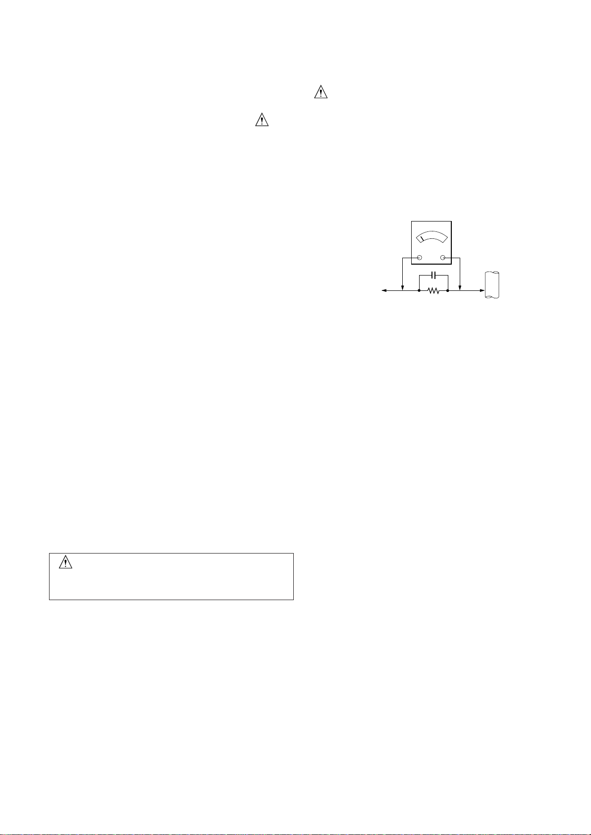
Leakage Current Hot Check Circuit
AC Volt-meter
Good Earth Ground
such as WATER PIPE,
To Instrument's
exposed
METALLIC PARTS
When 25A is impressed between Earth and 2nd Ground
for 1 second, Resistance must be less than 0.1
Adjustment standard
*Base on
0.15uF
1.5 Kohm/10W
CONDUIT etc.
Ω
• Make certain that treatment person’s body are grounded
through wrist band.
• Do not leave the module in high temperature and in areas of
high humidity for a long time.
• The module not be exposed to the direct sunlight.
• Avoid contact with water as it may a short circuit within the
module.
• If the surface of panel become dirty, please wipe it off with a
softmaterial. (Cleaning with a dirty or rough cloth may damage
the panel.)
CAUTION
Please use only a plastic screwdriver to protect yourself
from shock hazard during service operation.
Copyright ©
Only for training and service purposes
2010 LG Electronics. Inc. All right reserved.
- 3 -
LGE Internal Use Only
Page 4

SERVICING PRECAUTIONS
CAUTION: Before servicing receivers covered by this service
manual and its supplements and addenda, read and follow the
SAFETY PRECAUTIONS on page 3 of this publication.
NOTE: If unforeseen circumstances create conflict between the
following servicing precautions and any of the safety precautions on
page 3 of this publication, always follow the safety precautions.
Remember: Safety First.
General Servicing Precautions
1. Always unplug the receiver AC power cord from the AC power
source before;
. Removing or reinstalling any component, circuit board
a
module or any other receiver assembly.
b. Disconnecting or re-connecting any receiver electrical plug or
other electrical connection.
c. Connecting a test substitute in parallel with an electrolytic
capacitor in the receiver.
CAUTION: A wrong part substitution or incorrect polarity
installation of electrolytic capacitors may result in an
explosion hazard.
2. Test high voltage only by measuring it with an appropriate high
voltage meter or other voltage measuring device (DVM,
FETVOM, etc) equipped with a suitable high voltage probe.
Do not test high voltage by "drawing an arc".
3. Do not spray chemicals on or near this receiver or any of its
assemblies.
4. Unless specified otherwise in this service manual, clean
electrical contacts only by applying the following mixture to the
contacts with a pipe cleaner, cotton-tipped stick or comparable
non-abrasive applicator; 10% (by volume) Acetone and 90% (by
volume) is opropyl alcohol (90%-99% strength)
CAUTION: This is a flammable mixture.
Unless specified otherwise in this service manual, lubrication of
contacts in not required.
5. Do not defeat any plug/socket B+ voltage interlocks with which
receivers covered by this service manual might be equipped.
6. Do not apply AC power to this instrument and/or any of its
electrical assemblies unless all solid-state device heat sinks are
correctly installed.
7. Always connect the test receiver ground lead to the receiver
chassis ground before connecting the test receiver positive
lead.
Always remove the test receiver ground lead last.
8. Use with this receiver only the test fixtures specified in this
service manual.
CAUTION: Do not connect the test fixture ground strap to any
heat sink in this receiver.
Electrostatically Sensitive (ES) Devices
Some semiconductor (solid-state) devices can be damaged easily
by static electricity. Such components commonly are called
Electrostatically Sensitive (ES) Devices. Examples of typical ES
devices are integrated circuits and some field-effect transistors and
semiconductor "chip" components. The following techniques
should be used to help reduce the incidence of component
damage caused by static by static electricity.
1. Immediately before handling any semiconductor component or
semiconductor-equipped assembly, drain off any electrostatic
charge on your body by touching a known earth ground.
Alternatively, obtain and wear a commercially available
discharging wrist strap device, which should be removed to
prevent potential shock reasons prior to applying power to the
unit under test.
2. After removing an electrical assembly equipped with ES
devices, place the assembly on a conductive surface such as
aluminum foil, to prevent electrostatic charge buildup or
exposure of the assembly.
3. Use only a grounded-tip soldering iron to solder or unsolder ES
devices.
4. Use only an anti-static type solder removal device. Some solder
removal devices not classified as "anti-static" can generate
electrical charges sufficient to damage ES devices.
5. Do not use freon-propelled chemicals. These can generate
electrical charges sufficient to damage ES devices.
6. Do not remove a replacement ES device from its protective
package until immediately before you are ready to install it.
(Most replacement ES devices are packaged with leads
electrically shorted together by conductive foam, aluminum foil
or comparable conductive material).
7. Immediately before removing the protective material from the
leads of a replacement ES device, touch the protective material
to the chassis or circuit assembly into which the device will be
installed.
CAUTION: Be sure no power is applied to the chassis or circuit,
and observe all other safety precautions.
8. Minimize bodily motions when handling unpackaged
replacement ES devices. (Otherwise harmless motion such as
the brushing together of your clothes fabric or the lifting of your
foot from a carpeted floor can generate static electricity
sufficient to damage an ES device.)
General Soldering Guidelines
1. Use a grounded-tip, low-wattage soldering iron and appropriate
tip size and shape that will maintain tip temperature within the
range or 500ºF to 600ºF.
2. Use an appropriate gauge of RMA resin-core solder composed
of 60 parts tin/40 parts lead.
3. Keep the soldering iron tip clean and well tinned.
4. Thoroughly clean the surfaces to be soldered. Use a mall wirebristle (0.5 inch, or 1.25cm) brush with a metal handle.
Do not use freon-propelled spray-on cleaners.
5. Use the following unsoldering technique
a. Allow the soldering iron tip to reach normal temperature.
(500ºF to 600ºF)
b. Heat the component lead until the solder melts.
c. Quickly draw the melted solder with an anti-static, suction-
type solder removal device or with solder braid.
CAUTION: Work quickly to avoid overheating the circuit
board printed foil.
6. Use the following soldering technique.
a. Allow the soldering iron tip to reach a normal temperature
(500ºF to 600ºF)
b. First, hold the soldering iron tip and solder the strand against
the component lead until the solder melts.
c. Quickly move the soldering iron tip to the junction of the
component lead and the printed circuit foil, and hold it there
only until the solder flows onto and around both the
component lead and the foil.
CAUTION: Work quickly to avoid overheating the circuit
board printed foil.
d. Closely inspect the solder area and remove any excess or
splashed solder with a small wire-bristle brush.
Copyright ©
Only for training and service purposes
2010 LG Electronics. Inc. All right reserved.
- 4 -
LGE Internal Use Only
Page 5

IC Remove/Replacement
Some chassis circuit boards have slotted holes (oblong) through
which the IC leads are inserted and then bent flat against the
circuit foil. When holes are the slotted type, the following technique
should be used to remove and replace the IC. When working with
boards using the familiar round hole, use the standard technique
as outlined in paragraphs 5 and 6 above.
Removal
1. Desolder and straighten each IC lead in one operation by gently
prying up on the lead with the soldering iron tip as the solder
melts.
2. Draw away the melted solder with an anti-static suction-type
solder removal device (or with solder braid) before removing the
IC.
Replacement
1. Carefully insert the replacement IC in the circuit board.
2. Carefully bend each IC lead against the circuit foil pad and
solder it.
3. Clean the soldered areas with a small wire-bristle brush.
(It is not necessary to reapply acrylic coating to the areas).
"Small-Signal" Discrete TransistorRemoval/Replacement
1. Remove the defective transistor by clipping its leads as close as
possible to the component body.
2. Bend into a "U" shape the end of each of three leads remaining
on the circuit board.
3. Bend into a "U" shape the replacement transistor leads.
4. Connect the replacement transistor leads to the corresponding
leads extending from the circuit board and crimp the "U" with
long nose pliers to insure metal to metal contact then solder
each connection.
Power Output, Transistor Device
Removal/Replacement
1. Heat and remove all solder from around the transistor leads.
2. Remove the heat sink mounting screw (if so equipped).
3. Carefully remove the transistor from the heat sink of the circuit
board.
4. Insert new transistor in the circuit board.
5. Solder each transistor lead, and clip off excess lead.
6. Replace heat sink.
Circuit Board Foil Repair
Excessive heat applied to the copper foil of any printed circuit
board will weaken the adhesive that bonds the foil to the circuit
board causing the foil to separate from or "lift-off" the board. The
following guidelines and procedures should be followed whenever
this condition is encountered.
At IC Connections
To repair a defective copper pattern at IC connections use the
following procedure to install a jumper wire on the copper pattern
side of the circuit board. (Use this technique only on IC
connections).
1. Carefully remove the damaged copper pattern with a sharp
knife. (Remove only as much copper as absolutely necessary).
2. carefully scratch away the solder resist and acrylic coating (if
used) from the end of the remaining copper pattern.
3. Bend a small "U" in one end of a small gauge jumper wire and
carefully crimp it around the IC pin. Solder the IC connection.
4. Route the jumper wire along the path of the out-away copper
pattern and let it overlap the previously scraped end of the good
copper pattern. Solder the overlapped area and clip off any
excess jumper wire.
At Other Connections
Use the following technique to repair the defective copper pattern
at connections other than IC Pins. This technique involves the
installation of a jumper wire on the component side of the circuit
board.
1. Remove the defective copper pattern with a sharp knife.
Remove at least 1/4 inch of copper, to ensure that a hazardous
condition will not exist if the jumper wire opens.
2. Trace along the copper pattern from both sides of the pattern
break and locate the nearest component that is directly
connected to the affected copper pattern.
3. Connect insulated 20-gauge jumper wire from the lead of the
nearest component on one side of the pattern break to the lead
of the nearest component on the other side.
Carefully crimp and solder the connections.
CAUTION: Be sure the insulated jumper wire is dressed so the
it does not touch components or sharp edges.
Diode Removal/Replacement
1. Remove defective diode by clipping its leads as close as
possible to diode body.
2. Bend the two remaining leads perpendicular y to the circuit
board.
3. Observing diode polarity, wrap each lead of the new diode
around the corresponding lead on the circuit board.
4. Securely crimp each connection and solder it.
5. Inspect (on the circuit board copper side) the solder joints of
the two "original" leads. If they are not shiny, reheat them and if
necessary, apply additional solder.
Fuse and Conventional Resistor
Removal/Replacement
1. Clip each fuse or resistor lead at top of the circuit board hollow
stake.
2. Securely crimp the leads of replacement component around
notch at stake top.
3. Solder the connections.
CAUTION: Maintain original spacing between the replaced
component and adjacent components and the circuit board to
prevent excessive component temperatures.
Copyright ©
Only for training and service purposes
2010 LG Electronics. Inc. All right reserved.
- 5 -
LGE Internal Use Only
Page 6
1. General Specification
Co
ntent
SPECIFICATIONS
Item
No
1 C
2 Us
3 Sal
4 Fe
5 Ch
6
7
er Model Name
neral
Ge
Scope
Pow
u
stomer BRAND
29UM55
e region Refer to Suffix standard
ature 29” Wide LCD MONITOR
assis Name LM14P
External SW
&Adj.
nction Picture Mode Ratio, ECO(Super Energy Saving), Six
Fu
er Cord
DVI
MI
HD
LEFT, RIGHT, UP, DOWN, CENTER
Color, Audio Volume(Headphone),
Length : 1.55±0.05 M
Shape : Wall-out
Color : Black
Weight : 130g
Length :
Shape :
Color :
Pin :
Length : 1.8m
Shape : Detachable Type
Color : Black
Weight : 102g
Rem
Refer to Suffix
standard and power
cord table
Do not Support
Support
ark
8 Ca
9 Pow
10
Applying module list
1
Etc (accessory) Manual CD - Support
1
ble
er
Length :
USB
io
Aud
TV
Length : ,Shape : ,Color: ,Pin Do not Support
Shape :
Color :
Length :
Shape :
Color:
Input: AC100~240V 50~60Hz,1.2A Max
Output: DC 19V 2.1A
Adapter
Weight : 190g
P/No Specification
987701 LM290WW2-SSA1
EAJ62
Do not Support
Do not Support
40W
Copyright ©
Only for training and service purposes
2010 LG Electronics. Inc. All right reserved.
- 6 -
LGE Internal Use Only
Page 7
2. Mechanical specification
Rem
ark
No Item Content Remark
Width (W) Length (D) Height (H)
Before Packing 703.0mm 213.2mm 414.2cm With stand
ct
1
2
Produ
Dimension
ct
Produ
Weight
703.0mm 64.0mm 328mm Without stand
After Packing
814mm 405mm 156mm
Only SET 5.2kg Without stand : 4.7kg
With BOX
7.5Kg
3
Con
tainer
Loading
Quantity
4 Sta
nd
Assy
5 Appe
arance General Refer to Standard of LG(56)G2-1011
3. Optical Character
No I
Vie
1
2
3
4 Res
wing Angle
<CR≥10>
L
nance(휘도)
umi
Con
trast Ratio(명암 비)
ponse Time On/off:14ms(TYP, GTG),
Individual
(Vertical Type)
20ft 40ft
Ind
i. Pallet Indi.
525
462 1,080 966
Wood
en
Face_up
40ftH/C
- Indi. : 1,296
- Pallet : 1,152
Type Base detachable
Size
(W x D x H) 124mm x 213.2mm x 42.6mm Only stand ass’y
Til
t Degree
t force F1 /F2 :1.0 ~ 1.5kgf
Til
ding Degree9 None
Fol
tem Criteria
Horizontal(R/L) : +89º/-89º ( (Typ.)
ical(Top/Bottom) : +89º/-89º (Typ.)
Vert
Average Luminance
2
(cd/m
Ave
rage Luminance
2
(cd/m
rage Luminance
Ave
2
(cd/m
r Energy
Supe
Saving On
Lumi
nance
Uniformity
700(MIN), 1000(TYP),
DFC->5,000,000:1(Typ.) / 4,000,000:1(Min)
(It is measured at center point)
-5°(+/-3°)~ +20°(+/-3°)
20
n), 250 (Typ.)
0(mi
)
)
)
(Full white pattern, 0.7V)
1
(min)
70
(Full white pattern, 0.7V)
150(mi
n)
(Full white pattern, 0.7V)
Max 25% down from S-Energy Saving Off.
75%(min),
Warm
(6500K)
Medium
(8000K)
Cool
(9300K)
Whit
e
e W
Whit
e
Whit
RED
GREEN
E
BLU
5
IE
Color
C
Coordinates
(색 좌표)
Copyright © 2010 LG Electronics. Inc. All right reserved.
Only for training and service purposes
Minimum Nor mal Maximum
W
X
T
.03
WY 0.329
WY 0.3
W
WY
R
X
RY
G
X
GY
B
X
BY
yp-0
Typ-0
X
X
Typ-0
Typ-0
.03 0.295 Typ+0.03 Medium
.03
.03
0.313
05
0.283
.2
98
0
0.660
0.331
0.306
0.609
0.149
0.
062
- 7 -
Typ+0.03
Typ+0.03
Typ+0.03
Warm
(6500K)
(8000K)
Cool
(9300K)
Warm
(6500K)
LGE Internal Use Only
Page 8
4. Engineering Specification
p
ported Sync. Type
1
2 Op
3 Re
4 In
Su
erating Frequency
solution
put Voltage Voltage :100 – 240 Vac, 50 or 60Hz, 1.0A
5 Inrush Current Cold Start : 50 A Hot : 120 A
6
Op
erating Condition
On
Mode
Separate Sync.
Horizontal
MI
HD
DP
HD
MI
DP
Sync
(H/V)
H
Re
Re
Video LED Wattage
On/On Active
/On Active
On
30 ∼ 90kHz
Ve
rtical
orizontal
Ve
rtical 50 ~ 75 Hz
(AV)25~60 Hz,
(PC)50~75 Hz
30 ∼ 90kHz
Max. 2560×1080 @ 60Hz
commend 2560×1080 @ 60Hz
Ma
x. 2560×1080 @ 60Hz
commend 2560×1080 @ 60Hz
ite
Wh
Wh
ite
4
W(Typ)
3
39W
(
Max)
Test condition
1.2560x1080@60Hz
2. burst pattern
3. 100~240V
4. After aging 30min
Adjust brightness
controls until the
luminance of the
Wh
EPA6
.0 On/On Active
Off/On
Sle
ep Mode
On/Off
Off
Off/Off
f Mode
Of
(Power switch off)
ECO
MT
7
BF
Us
8
ing Altitude
- - Off < 0.5W
High,
Low,Off
Low
High
30,000 HRS with 90%
Confidence level
5,000 m (for Reliability) 3,000m(for FOS)
ite
h
ite
W
Blinking
ite
Wh
P
A spec
E
31
.69 W
0.5W
<
iciency
Eff
15±5% (3W/h)
25±5% (5W/h)
Lamp Life : 30,000 Hours(Min)
screen is 200(cd/m2).
-Test Condition
(1)
Env
9
iron
ment
Conditio
n
OSD
0peratin
g
Sto
rage
MENU Brightness 1 - 100
Temperature
midity 10% ~ 80%
Hu
Temperature
H
midity 5% ~ 90% non-condensing
u
10 °C ~ 35 °C
-20 °C ~ 60 °C
Copyright ©
Only for training and service purposes
2010 LG Electronics. Inc. All right reserved.
- 8 -
LGE Internal Use Only
Page 9
VOL
UME
T
R
EBLE
(Monitor
MENU
block)
set Reset/Cancel
Re
MENU
(AV/TV
block)
Copyright ©
Only for training and service purposes
2010 LG Electronics. Inc. All right reserved.
Contrast 1 – 100
ume 1 – 100, Mute
Vol
put HDMI1 / HDMI2/ DP
In
Wide / Cinema1 /
tio
Ra
Cinema2 / Original /
ECO High, Low, Off
Reader1, Reader2,
Custom, Photo,
Cinema, Game
Fu
nc.
ader mode
Re
c
ture Mode
Pi
PBP On
Main: HDMI1, HDMI2,
DP
b
: HDMI1, HDMI2,
Su
DP
PBP
PBP
n
put
I
io HDMI1, HDMI2, DP
Aud
p On, Off
Swa
Full On, Off
Sub
tio Main
Ra
tio Sub
Ra
Sharpness 0 - 10
Pic
Co
ture
lor
ck Level
sponse
Re
Time
Gamma
Co
lor Temp
Re
d 0 - 100
Gre
en 0 – 100
Blu
e 0 – 100
Six
Color
(BLACK LEVEL enable
at HDMI input)
High, Middle, Low
Gamma0, Gamma1,
Warm, Medium, Cool,
Bla
(Hue,
Saturation)
nguage
La
AV Mode N/A
PC/
n Audio HDMI1/HDMI2,DP
Mai
ton Sound N/A
But
er LED On / Off
Pow
1.2 On / Off
DP
Lock On / Off
OSD
CHANNEL
2~69(AIR) / 1 ~ 125(CABLE)
/DEL CH ADD/DELETE
CHANNEL
AD
JUSTMENT
AU
DIO
UP
SET
ADD
O CHANNEL ON/OFF
AUT
SELEC
FI
CONTRAST 0~100
BRI
S
SHAR
CO
TI
BASS
MUT
SOU
MON
LANGUAGE▶
English/German/French/Esperanto
Italian/Korean…
IMA
OSD
T
CY
T AIR/CABLE
NE TUNE 0 ~ 100
GHTNES
PNESS 0~100
LOR 0~100
NT 0~100
E ON/OFF
ND
O/STEREO
GE SIZE ▶ FULL/1:1
POSITION
R
ANSPAREN
0~100
0~
100
A
N/
/
A
N
0~100
- 9 -
1:1
Reader Off
, Off
Low, High
Gamma2
Custom
0 - 100
de, Original
Wi
de, Original
Wi
16 Language:
English,
Germanic,
French, Spanish,
Italian, Swedish,
Finnish,
Portuguese
Brazilian
Portuguese,
Polish, Russian,
Greek, Chinese,
Japanese,
Korean,
Function Support:
No
Function Support:
No
Function Support:
No
Function Support:
No
LGE Internal Use Only
Page 10

5. Applying module Character
Co
ntent
Item
No
Maker LGD
e IPS
D Module
LC
1
Feature
andard Measurement Condition
St
Typ
ve Display Area 29 inches(73.025cm) diagonal (21:9)
Acti
x
el Pitch [mm]
Pi
e
ctrical Interface 2ch-LVDS(41P), 2ch-LVDS(51P)
El
lor Depth 6-bit + A-FRC, 16.7M colors
Co
(Outline) [mm]
Size
Sur
face Treatment
erating Mode Transmissive mode, normally Black
Op
light Unit White LED
Back
T
R/
.
0876(H)mm x RGB x 0.2628(V)mm
0
602.2(H) x 271.1(V) x16.5(D) (Typ.)
Hard coating (3H) & Anti-Glare treatment
of the front polarizer
Typical 14ms
28ms
Max.
Rem
ark
n Ambient Luminance Level : dark ( < 10 lux)
n Ambient Temperature : Normal Temperature(10 ~ 25 ℃)
n warm-up Time : More than 30min (at Full White Pattern)
n Input Signal : 2560X1080@60Hz
n Contrast : 70
n Brightness : Max. 100
n 6500K : Color Temperature Setting is 6500 K( if it’s not special specification)
n Clock/Clock Phase : The Best Setting
l Another Spec.: Product Specification Standard( LG(55)G1-1034 )
l Cosmetic Spec. : LCD Module IIS Spec.
5.1 Display Area
1) Active Display Area of the LCD Monitor Should be within Cabinet’s Bezel.
2) Distance Difference between Active Area and Bezel
| A-B|<1.0 mm , | C-D|<1.0 mm
A: The Distance from The Left of Active Area to the Bezel
B: The Distance from The Right of Active Area to the Bezel
C: The Distance from The Top of Active Area to the Bezel
D: The Distance from The Bottom of Active Area to the Bezel
Active area
A
A A B
C
Copyright ©
Only for training and service purposes
2010 LG Electronics. Inc. All right reserved.
D
- 10 -
Bezel
LGE Internal Use Only
Page 11

6. EDID
6.1
29
UM55
No Item Content 16진 Data
1 Man
2 Prod
3 Y
4 V
5 Re
6 Seri
7 We
8 Mo
9 Ch
10
Special Item Need to Input Serial Number
**
Protocol : DDC 2AB
Da
ta ( 128 Bytes ) à29UM55
EDID Ver. 1.3 FOR HDMI 1 (256Byte)
ufacturer ID GSM 1E 6D
uct ID
e
ar 2014
e
rsion 1 01
vision
al Number * *
e
k ** **
d
el Name LG ULTRAWIDE --
eck Sum **** ****
(HDMI)
(Display Port)
HDMI : 3
DP : 4
23025(F1 59)
23026(F2 59)
03
04
Copyright ©
Only for training and service purposes
2010 LG Electronics. Inc. All right reserved.
- 11 -
LGE Internal Use Only
Page 12

D Ver. 1.3 FOR HDMI 2 (256Byte)
EDI
EDID Ver. 1.4 FOR Display Port (256Byte)
Copyright ©
Only for training and service purposes
2010 LG Electronics. Inc. All right reserved.
- 12 -
LGE Internal Use Only
Page 13

(1) Signal(Video & Sync)
deo
Vi
Sync
TIMING CHART
C
B
(2)
H
V Timing
/
HD
mode section
xels) -
1
2
H(Pi
nes)
V(Li
xels) -
H(Pi
nes)
V(Li
H(Pixels) -
3
V(Li
nes)
H(Pixels) +
4
5
6
nes)
V(Li
H(Pi
xels) +
nes)
V(Li
H(Pi
xels) nes)
V(Li
MI/DP
polar
ity
DE
DOT
CLOCK
[MHz]
28.321
+
25.175
-
-
+
+
-
31.5
40.0
49.5
65.0
F
A
Frequency
[kHz]/[Hz]
Total
Period
(E)
Display
(A)
Front
Porch
(D)
Sync.
(C)
31.468 900 720 18 108 54
70
.08
44
9
40
0
12
2
31.469 800 640 16 96 48
59
.94
52
5
48
0
10
2
37.5 840 640 16 64 120
75
50
0
48
0
1
3
37.879 1056 800 40 128 88
60
.317
62
8
60
0
1
4
46.875 1056 800 16 80 160
75
.0
62
5
60
0
1
3
48.363 1344 1024 24 136 160
60
.0
80
6
76
8
3
6
Back
Porch
(B)
35
33
16
23
21
29
Resolution
720 X 400
640 x 480
640 x 480
800 x 600
800 x 600
1024 x 768
7
8
9
10
11
12
13
14
15
H(Pi
V(Li
H(Pi
V(Li
H(Pi
V(Li
H(Pixels) +
V(Li
H(Pi
V(Li
H(Pixels) +
V(Li
H(Pi
V(Li
H
(Pi
V(Li
H(Pixels) -
V(Lines) +
xels) +
nes)
+
78.75
xels) +
nes)
+
108
xels) +
nes) + 60 750 720 5 5 20
74.25
60.123 1312 1024 16 96 176
75
.029
80
0
76
8
1
3
28
67.5 1600 1152 64 128 256
75
90
0
86
4
1
3
32
45 1650 1280 110 40 220
63.981 1688 1280 48 112 248
nes)
+
xels) +
nes)
+
nes) + 60.00 1000 900 1 3 96
xels) -
nes)
+
xels) +
-
nes)
108
135
108.0
146.25
148.50
60
.02
10
66
10
24
1
3
38
79.976 1688 1280 16 144 248
75
.025
10
66
10
24
1
3
38
60.00 1800 1600 24 80 96
65.29 2240 1680 104 176 280
59
.954
10
89
50
10
3
6
30
67.50 2200 1920 88 44 148
60
11
25
10
4
80
5
36
66.7 2784 2560 64 64 96
185.58
60 1111 1080 3 10 18
1024 x 768
1152 x 864
1600 x 900
1280x720
1280 x
1024
1280 x
1024
1680 x
1050
1920 x
1080
2560 x
1080
l DVI
: DTV Mode is not supported (interlace mode)
Copyright ©
Only for training and service purposes
2010 LG Electronics. Inc. All right reserved.
- 13 -
LGE Internal Use Only
Page 14

(3)
MI Video
HD
in
put
ctory support
Fa
mode
(Pres
1 48
2 57
3 72
4 72
5 10
6 10
rizontal
et Mode)
Ho
frequency
(KHz)
Vert
frequency
(Hz)
0P 31.5 60
6P 31.25 50
0P 37.5 50
0P 45 60
80P 56.25 50
80P 67.5 60
ical
Copyright ©
Only for training and service purposes
2010 LG Electronics. Inc. All right reserved.
- 14 -
LGE Internal Use Only
Page 15

ADJUSTMENT
1. Coverage
Apply to 73.025
Gumi Korea) or made in accordance with the standard of Gumi
Factory process.
Wide monitor made in Monitor Factory
cm
2. Appointment
2.1 Adjustment must be done as fixed sequence, and adjustment
sequence can be modified after agreement withthe responsible
R&D engineer considering mass-production condition.
2.2 Power : AC 100 - 240 Voltage (Free)
2.3
Input signal:
2.3.1 RGB Input: As Product Standard (Signal ROM : LB800K
Ver1.6)
2
.3.2 RJ-45 input : As Product Standard (Ethernet connection
through network from Host PC)
* PC spec for MK(Minikey) Loader (TBD): CPU - Dual core 2.0
GHzD, Memory - 2 GByteD
*PC spec for Host PC (TBD): CPU - Dual core 2.0 GHzD,
Memory - 2 GByteD
2.4 Warm-up Time: Over than 30 minutes
.
5 Adjustment
2
Display adjust equipment, VG-813(or VG819), Oscilloscope,
PC (More than 486
program.
equipment : White balance equipment (CA-110),
computer ) & White balance adjust
3. Adjustment
3.1 Overview
Use factory automation equipment and adjust automatic
movement. But, do via passivity adjust in erroroccurrence.
PC audio volume : MAX
* LAN cable
* Router
*
PC: vSpace S/W for N+ ( Ver 4.5.xx.xx ) --- Caution: Ver
4.4.xx.xx for N1742L family
3.2.2 Total Assembly Line
· Ready : Heat-run during5 minutes in the state with signal
Connect input signal to D-sub.
·
· Default value before adjustment : Contrast “70” , Brightness
‘100(Max)”
3.2.3 Adjustment of Horizontal/Verticality screen
position, Clock and Clock Phase at each Mode.
· There is no special factory mode adjustment. Writing initial value
of EEPROM in Board Assembly
and Reset mode. (EEPROM is initialized when AC Power is
ON first.)
· If the change of FOS data is needed after M.P, it is possible by
writing Mode Data with EEPROM write command or modifying
the Mode Data in MICOM itself.
line is adjusting Preset Mode
3.2.4 Color coordinates adjustment and Luminance
adjustment.
3.2.4.1 Color coordinates adjustment
· Monitor Contrast / Brightness
- Contrast : 70
- Brightness : 100(Max)
· CA-110: Set “channel 9”
· Signal Generator : At cut-off and drive --> 16 step pattern for
ADC (Program No.: 31)
- Output Voltage : 700 mVp-p
- Output Mode : Mode 12 (SXGA 60 Hz)mode Setting.
3.2 Adjustment order
(refer to the Adjustment standard and adjustment command table)
3.2.1 Board Assembly Line
3.2.1.1 15pin D-sub (RGB)
· Connect input signal to 15pin D-sub.
· Check the firmware version & model name. And write the
firmware code to the serial Flash ROM by ISP.
· Ready for adjustment : check whether adjustment command
works normally or not and the operating state of each mode.
· Check the display state of gray color when 256 gray scale
patterns is embodied.
· Read by EEPROM Read Command to check whether initial
value is correct or not.
3.2.1.2 MK( Minikey ) Loading
· Open MK Loader Tool on MK Loader PC.
( * MK Loader PC should be connected Internet)
· Connect input signal to RJ-45 input with LAN cable connected
network devices such as routers.
· Turn on the Monitor set.
· Click the box when the °∞empty port °∞box is changed to “write
mini-key” in MK Loader Tool.
3.2.1.2 RJ-45 input
· Connect input signal to RJ-45 input with LAN cable connected
network devices such as routers.
· Check USB 1.1 Port (Keyboard/ Mouse) : @RJ-45 input
· Check USB 2.0 Port (USB Memory Stick 2port) : @RJ-45 input
· Check Audio (Ear-phone out/ Mic in/ Speaker) : @RJ-45 input,
3.2.4.2.Adjustment : Board Assembly Line
· Select RGB mode
16 step pattern for ADC (Program No.31 (Mode 12,Pattern
· Input
11)). (Video level : 700 mVp-p)
· Adjust by commanding AUTO_COLOR_ADJUST
· Confirm “Success” message in Screen or Check the data of
0xFE, 0xFF address of EEPROM(0XA6) is 0xAA after waiting 5
seconds.
· If there is “FAULT” message or the data of 0xFE, 0XFF address
of EEPROM(0xA6) is not 0xAA, do adjust again.
· If all Adjustment is completed, the values of 6500K, User Color
and 9300K are saved automatically.
· Select RGB mode
· Input 16 step pattern for ADC (Program No.31 (Mode 12,Pattern
11)). (Video level : 700mVp-p)
· Adjust by commanding AUTO_COLOR_ADJUST
· Confirm “Success” message in Screen or Check the data of
0xFE,0xFF address of EEPROM(0xA6) is 0xAA after waiting 5
seconds.
3.2.4.3. Confirm at Total Assembly Line: adjustment
· Check the data of 0xFE, 0xFF address of EEPROM(0xA6) is
0xAA.
If the data of 0XFE, FF address of EEPROM(0xA6) is not
·
0xAA, do adjust again by 3.2.4.2.
Copyright ©
Only for training and service purposes
2010 LG Electronics. Inc. All right reserved.
- 15 -
LGE Internal Use Only
Page 16

2.4.4. Confirm PRESET 6500K Color coordinates and Adjust
3.
PRESET 9300K Color coordinates .
· Set as Aging mode ON, by commanding AGING_ON/OFF
command code.
· Select Module that is being used in present production by
commanding MODULE SELECT. ( It is not needed so far.
However, it will be needed to apply other modules)
· Send SYSTEM RESET command to set Module data.
· Input Full White Pattern (Video level : 700 mVp-p)
· Set as 9300K by commanding COLOR_MODE_CHANGE
Command code.
· Check to meet x = 0.283 ± 0.03, y=0.298 ± 0.03, and confirm.
· Only if it does not meet, adjust as below steps.
· Adjust to meet x = 0.283 ± 0.01, y=0.298 ± 0.01 in 5 minutes. and
confirm.
· Save 9300K Color by commanding COLOR SAVE Command
code.
· Set as 6500K by commanding COLOR_MODE_CHANGE
Command code.
· Check to meet x = 0.313 ± 0.03, y=0.329 ± 0.03, and confirm.
· Only if it does not meet, adjust as below steps.
· Adjust to meet x = 0.313 ± 0.01, y =0.329 ± 0.01, and confirm.
· Save 6500K Color by commanding COLOR SAVE Command
code.
· Set as sRGB by commanding COLOR_MODE_CHANGE
Command code.
· Adjust to meet Y = 150 ± 50, and confirm.
· Save sRGB Color by commanding COLOR SAVE Command
code.
3.2.4.5. Confirm User color coordinates .
· Confirm Whether User color is saved same as 6500K.
· After confirming Color coordinates, Must return to 6500K
3.2.5 Confirm Operation state.
3.2.5.1 Operation mode : Confirm whether each appointed mode
operate correctly or not.
3.2.5.2 Confirmation of Adjustment condition and operation :
Confirm whether it meet Auto/Manual equipment Adjustment
standard or not.
· Confirm Analog screen state : Confirm screen state at below
mode.
Appointment mode (RGB input):
640*480 @60Hz (Mode 1),
800*600@75Hz(Mode 5),
1024*768@60Hz(Mode 8),
1280*1024@60Hz(Mode 12),
SMPTE pattern(Check 0%,5%,95%,100%)
–Mode can be added.
3.2.5.3. Confirm Auto adjustment operation.
· Input Analog 1 Dot on/off & Rectangle Pattern at Mode
12(1280x1024@60 Hz)
· Confirm adjustment operation by changing Clock, Phase, H/V
Position.
· Check Clock, Phase by pressing AUTO Key.
· Confirm first set of new lot by periods
3.2.5.4 Other quality
· Confirm that each items satisfy under standard condition that was
written product spec.
· Confirm Applying Module & MICOM Setting --> Confirm with
Service OSD
- Confirm at Service OSD by “Menu + Power key” on .(from
Power off)
- Confirm first set of new lot by periods, and confirm periodically
when there is Process change or Adjustment setting change.
3.2.5.5. OSD & Adjustment device Confirmation : Confirm
operation mentioned as product spec.
· Vary Brightness and Contrast and confirm the variation of
Luminance and display status.
· Operate the f-engine function and confirm variation of Luminance.
· Make sure to do FACTORY RESET after confirmation of OSD
function.
3.2.5.6. Confirm the display state by inputting 8 color Bar Pattern &
256 Gray Scale pattern.
3.2.5.7. DPM operation confirmation : Check if Power LED Color
and Power Consumption operates as standard.
· Measurement Condition : 230 V@ 50 Hz (Analog)
· Confirm DPM operation at the state of screen without Video
Signal.
3.2.5.8. RJ-45 input
· Connect input signal to RJ-45 input with LAN cable connected
network devices such as routers.
· Check USB 1.1 Port (Keyboard/ Mouse) : @RJ-45 input
· Check USB 2.0 Port (USB Memory Stick 2port) : @RJ-45 input
· Check Audio (Ear-phone out/Mic in/Speaker) : @RJ-45 input, PC
audio volume : MAX
* LAN cable
* Router
* PC: vSpace S/W for N+ ( Ver 4.5.xx.xx ) --- Caution: Ver
4.4.xx.xx for N1742L family
3.2.5.9. DDC EDID Write
( Set as Aging mode ON, by commanding AGING_ON/OFF
command code. )
1) SUFFIX: xxxxxPN
· Connect analog Signal Cable to D-sub wafer.
· Write EDID DATA to EEPROM(24C08) by using DDC2AB
protocol.
· Check whether written EDID data is correct or not.
(refer to Product spec).
--> After writing EDID, send Elapsed Time Clear command.
(Elapsed time should not be displayed, after EDID writing)
: Confirm periodically (in the first set of new lot, process change)
whether module name and aging time disappeared on the selfdiagnostics OSD with signal cable disconnected.
--> If Elapsed Time Clear command isn°Øt executed, module
name, aging time and TCO word appear on the self-diagnostics
OSD.(Module name and aging time should not appear after
writing EDID)
--> Make sure to do FACTORY RESET at the final process.
3.2.5.10. Shipping condition
· Contrast : 70
· Power Switch
· Brightness : “100(Max)”
· Color Select : Preset ( 6500K )
· Language Select : Refer to product spec.
· OSD Position : Center
· Power indicator : ON
· Flatron f-engine : Normal
: Off
Copyright ©
Only for training and service purposes
2010 LG Electronics. Inc. All right reserved.
- 16 -
LGE Internal Use Only
Page 17

4.Standard of Auto/Manual equipment adjustment
No
Category Class(Type) Rule Remark
ety UL UL60950-1 YES
Saf
CSA
1
EMC F
2
X-Ra
3
(CRT only)
Lo
4
Radiation
5 TC
Ergo
6
Etc
(Korea)
y
w
O
nomics ISO9241 (CRT) ISO9241-3, 7, 8 NO
(cUL) CSA C22.2 No.60950-1-03 YES
TU
V-GS(TUV-Type) EN60950-1 TUV-Type
O
SEMK
CE EN
EN60950-1 No
C
C CLASS B FCC 47 CFR Part 15 Class B YES
55022B, EN55024, EN61000-3-2, 3 YES
DHHS DHHS Rule 21 CFR Subchapter J N/A
C HWC Radiation Emitting Device ACT N/A
HW
MPR II MPR 1990:8; MPR 1990::01
TCO6.0 Emission, Ergonomics, Ecology, Energy
saving
ISO
13406-2 (LCD) ISO13406-2,ISO9241-307 NO
KC(SAFETY) Electric Supplies Safety Rule
(K60950)
NO
YES
NO
7
KC(EMC) MIC
CCC GB4943, GB9254, GB17625.1 YES
Etc
8
(China)
Te
st Hi-Pot 1500 V ac or 2121Vdc, 1 sec, under 10mA No
9
h Continuity 25 A, 1 sec, under 0.1 ohm No
Eart
10 EPA 6.0
11
EPEAT Gold
te
No
Energy Star 6.0
#3 - CRT monitor only
#4 – Different from Models
#5 – Different from Models
#6 - ISO9241-3, 7, 8 - CRT monitor only
ICO13406-2 / ISO 9241-307 - LCD monitor only
Ordinance 825
MIC Notice 100,Class B,
NO
Electric Article Technical Standard Ⅲ
Ene
rgy Star Display Version 6.0 YES
Yes
#7 –Safety Certification(안전인증) – Different from Models
* – Update to new standard regulation and Revision 3.0
Copyright ©
Only for training and service purposes
2010 LG Electronics. Inc. All right reserved.
- 17 -
LGE Internal Use Only
Page 18

5. Pattern for Adjustment
Pattern 0 : FULL BLACK (State of without video signal )
Pattern 1 : FULL WHITE (Don’t display other Character except for White Pattern)
Pattern 3 : FULL WHITE
Pattern 4 :
Pattern 5 : 1 Dot on, 1 Dot off & Rectangle Pattern
Pattern 6 : Vertical Sync only input (Use signal cable of which Pin #5 is GND)
Pattern 7 : Horizontal Sync only input (Use signal cable of which Pin #5 is GND)
Pattern 8 : State of without Vertical/Horizontal Sync and Video Signal. (Use signal cable of which Pin #5 is GND)
Pattern 9 : 8 Color Bar Pattern + 16 Gray Level Pattern
Pattern 10 : SMPTE Pattern
Pattern 11 : 16 Gray Step Pattern (700mV)
Cross hatch pattern (Horizontal 10Line, Vertcial 8Line) & Rectangle Pattern
Copyright ©
Only for training and service purposes
2010 LG Electronics. Inc. All right reserved.
- 18 -
LGE Internal Use Only
Page 19

BLOCK DIAGRAM (Main)
hFlash
Flas
AM
(1GB)
DDR2
SDR
AM
DDR2
SDR
(1GB)
tick
(Control Key)
Joys
Address[0:12]
DDR2
Address[0:12]
DDR2
DDR2 Data[0:15]
MemoryMemory
(2M)(2M)
SPI_DI
SPI_CSN
SPI_DO
SPI_WP
SPI_CLK
LVDS
41p
DDR2 Data[0:15]
Key1, Key2
A-out_L
A_out_R
phoneHeadphone
Head
TMDS
OM
EEPR
1HDMI 1
HDMI
el (2560x1080)
Pan
version)
TMDS
NT68370
LVDS
51p
WLED PDIM
WLED_ADIM
WLED_ENABLE
(E-
OM
EEPR
DPRXAUXN
DPRX_AUXP
2HDMI 2
HDMI
DPDP
Driver ICLED Driver IC
D
LE
DT1631SDT1631S
Copyright ©
Only for training and service purposes
2010 LG Electronics. Inc. All right reserved.
- 19 -
LGE Internal Use Only
Page 20

TROUBLESHOOTING GUIDE
1. NO POWER
`
X200
power issue
No
ADAPTER
CHECK
NO
ck JK500
Che
NO
IC100
Is
CRYSTAL X200
CK
CHE
PINN1,PINN2 PULSE
IC510-#3 IC509#3
IC100
CHECK
IC505 or IC506
CHECK IC500 or IC509 or
IC510
NO
S
YE
PIN4(19V)
IC500 PIN2(19V),PIN3(10V)
Is
YES
,IC510 PIN2(19V),PIN3(5V)
,IC509 PIN2(19V),PIN3(3.3V)
NO
IC505, PIN2(1.3V)
Is
CHECK
YES
IC506 PIN2(1.9V)
Copyright ©
Only for training and service purposes
2010 LG Electronics. Inc. All right reserved.
- 20 -
IC510-#2
LGE Internal Use Only
Page 21

2. NO RASTER (OSD IS NOT DISPLAYED) – MAIN
IC509 PIN3(3.3V)
CHECK
CHECK X200
1.
2. Trouble in IC100
CHECK CONNECTION From HDMI TO
IC100
NO
NO
NO
S
YE
12MHz
ck IC100 PIN
B19(3.3V)
Che
No Raster(OSD is not displayed)
00 PIN N1,N2
IC1
YES
CLK
IC100 PIN C14
Is
e in cable or LCD module
Troubl
Copyright ©
Only for training and service purposes
2010 LG Electronics. Inc. All right reserved.
- 21 -
LGE Internal Use Only
Page 22

3. TROUBLE IN DPM
Trouble in DPM
NO
ECK PC. PC is going to the DPM
CH
mode
k R133 AND R196
Chec
ECK HDMI CLK
CH
NO
S
YE
YES
IC100 PIN H4
Copyright ©
Only for training and service purposes
2010 LG Electronics. Inc. All right reserved.
- 22 -
Trouble in IC100
LGE Internal Use Only
Page 23

EXPLODED VIEW
IMPORTANT SAFETY NOTICE
Many electrical and mechanical parts in this chassis have special safety-related characteristics. These
parts are identified by in the Schematic Diagram and EXPLODED VIEW.
It is essential that these special safety parts should be replaced with the same components as
recommended in this manual to prevent X-RADIATION, Shock, Fire, or other Hazards.
Do not modify the original design without permission of manufacturer.
920
400
610
700
900
910
560
710
520
540
200
300
LV2
LV1
Page 24

1 6
IC100
RX1CBD1RX1CD2RX10BE1RX10E2RX11BF1RX11F2RX12BG1RX12G2RX2CBJ1RX2CJ2RX20BK1RX20K2RX21BL1RX21L2RX22BM1RX22M2RXAUX1NC1RXAUX1C2RXAUX2NH1RXAUX2H2BIN1+P2BIN1-P1SOGINR3GIN1+R2GIN1-R1RIN-T1RIN+T2HSYNCI0U1VSYNCI0U2RX3CB
NT68370(D VER.)
C126 1uF
C125 1uF
C124 1uF
C122 1uF
C121 1uF
C119 1uF
C118 1uF
C127 1uF
DP_AUXN
DP_AUXP
DP_RX0P
DP_RX0N
DP_RX1N
DP_RX1P
DP_RX2N
DP_RX2P
DP_RX3N
DP_RX3P
HDMI1_RX2-
HDMI1_RXC-
HDMI1_RX1-
HDMI1_RX0-
HDMI1_RX2+
HDMI1_RX1+
HDMI1_RX0+
HDMI1_RXC+
DP_RX1NDP_RX1N
D121
OPT
1
TMDS_CH1-
IP4283CZ10-TBA
[TVS DIODE FOR ESD PROTECTION]
DP_RX1P
DP_RX0N
3
2
TMDS_CH1+4TMDS_CH2-
GND_1
DP_RX1P
DP_RX0N
DP_RX0P
NC_17NC_28GND_29NC_310NC_4
6
5
TMDS_CH2+
DP_RX0P
D122
IP4283CZ10-TBA
D119
IP4283CZ10-TBA
D115
IP4283CZ10-TBA
DP_RX3N
OPT
1
DP_RX3N
DP_RX3P
2
TMDS_CH1-
DP_RX3P
HDMI2_RXC-
OPT
1
TMDS_CH1-
HDMI2_RXC-
HDMI2_RX1-
OPT
1
TMDS_CH1-
HDMI2_RX1-
TMDS_CH1+4TMDS_CH2-
HDMI2_RXC+HDMI2_RXC+
2
HDMI2_RX1+
2
HDMI2_RX1+
A15
B15
DP_RX2P
DP_RX2N
NC_17NC_28GND_29NC_310NC_4
6
3
5
TMDS_CH2+
GND_1
DP_RX2P
DP_RX2N
HDMI2_RX0+
6
3
TMDS_CH1+4TMDS_CH2-
5
GND_1
HDMI2_RX0- HDMI2_RX0-
HDMI2_RX0+
HDMI2_RX2-
6
3
TMDS_CH1+4TMDS_CH2-
5
GND_1
HDMI2_RX2+
HDMI2_RX2-
RX3C
RX30B
A14
NC_17NC_28GND_29NC_310NC_4
TMDS_CH2+
HDMI2_RX2+
NC_17NC_28GND_29NC_310NC_4
TMDS_CH2+
RX30
B14
RX31B
A13
B13
RX31
RX32B
RX32
A12
B12
D123
IP4283CZ10-TBA
D120
IP4283CZ10-TBA
.04
D116
IP4283CZ10-TBA
RX4CB
RX4C
A11
B11
HDMI2_RXC+
HDMI2_RXC-
DP_AUXN
OPT
1
TMDS_CH1-
DP_AUXN
HDMI1_RX1-
OPT
1
TMDS_CH1-
HDMI1_RX1-
HDMI1_RXC-
OPT
1
TMDS_CH1-
HDMI1_RXC-
RX40B
A10
B10
HDMI2_RX0-
DP_AUXP
2
DP_AUXP
HDMI1_RX1+
2
HDMI1_RX1+
HDMI1_RXC+
RX40
RX41BA9RX41B9RX42BA8RX42
B8
HDMI2_RX0+
HDMI2_RX2+
HDMI2_RX1-
HDMI2_RX2-
HDMI2_RX1+
DP_DET
3
GND_1
TMDS_CH1+4TMDS_CH2-
DP_DET
HDMI1_RX2-
3
TMDS_CH1+4TMDS_CH2-
GND_1
HDMI1_RX2-
HDMI1_RXC+
HDMI1_RX0-
3
2
TMDS_CH1+4TMDS_CH2-
GND_1
HDMI1_RX0-
DP_HPD
6
NC_17NC_28GND_29NC_310NC_4
5
TMDS_CH2+
DP_HPD
HDMI1_RX2+
NC_17NC_28GND_29NC_310NC_4
6
5
TMDS_CH2+
HDMI1_RX2+
HDMI1_RX0+
NC_17NC_28GND_29NC_310NC_4
6
5
TMDS_CH2+
HDMI1_RX0+
DP_RX0N
DP_RX1N
DP_RX2N
DP_RX3N
34UM65
Signal Input
DP_RX0P
100K
R164
100K
R162
100K
R160
100K
R158
DP_RX1P
DP_RX2P
DP_RX3P
100K
R165
100K
R163
100K
R161
100K
R159
HDMI_5V
+5V
A2CA1
D112
BAT54C
A2CA1
D109
BAT54C
IC101
M24C02-RMN6T
C107
0.1uF
16V
HDMI2_SCL
HDMI2_SDA
EDID_WP
R155
10K
D111
OPT
50V
C110
R128
10K
OPT
R127
10K
R126
10K
VCC
8
HDMI2
EEPROM
1
E0
68pF
D110
OPT
50V
C109
68pF
R125
33
R124
33
SDA6SCL7WC
5
3E22E14
VSS
DP_RX3P
DP_RX3N
ML_LANE_3+
ML_LANE_3-
GND_3
2
1
3
JK100
DP
62L020S-34A1N-7T0201-HF_
DP_RX2N
ML_LANE_2-
GND_2
4
DP_RX1N
DP_RX2P
ML_LANE_1-
ML_LANE_2+
7
6
GND_1
8
+3.3V
+3.3V
+3.3V
DP_RX0N
DP_RX1P
ML_LANE_1+
ML_LANE_0-
9
10
GND_0
11
DP_PLUG
R117 33
R110
1M
R108
10K
R153
10K
DP_RX0P
0
R100
CONFIG1
ML_LANE_0+
13512
0
R101
CONFIG2
14
DP_AUXP
C104 0.1uF 16V
AUX_CH+
15
HDMI2_DET
+3.3V
HDMI2_RXC-
0
R190
TMDS_CLK-
12
+3.3V
HDMI2_RXC-
0
CEC
CLK-11CLK_SHIELD
12
R195
10K
HDMI2_SCL
R1790R1800R182
HDMI2_SCL-1
RESERVED13CEC
SCL
14
15
R112
10K
HDMI2_SCL
0
R149
SCL
14NC13
15
1K
R181
HDMI_5V
HDMI2_SDA
HDMI2_SDA-1
DDC/CEC_GND
SDA
17
16
HDMI2_DET
1K
R168
HDMI_5V
HDMI2_SDA
R1670R169
SDA
DDC/CEC_GND
16
17
R192 1K
0
HOT_PLUG_DETECT
VDD[+5V]
19
18
R107 1K
0
HPD18+5V_POWER
19
C128
C102
0.1uF
20
0.1uF
20
16V
BODY_SHIELD
16V
SHIELD
HDMI2_HPD
33
R178
HDMI2_HPD
33
R140
10K
OPT
R191
D102
10K
OPT
R105
D108
THE SYMBOL MARK OF THIS SCHEMETIC DIAGRAM INCORPORATES
SPECIAL FEATURES IMPORTANT FOR PROTECTION FROM X-RADIATION.
FIRE AND ELECTRICAL SHOCK HAZARDS, WHEN SERVICING IF IS
ESSENTIAL THAT ONLY MANUFACTURES SPECIFIED PARTS BE USED FOR
THE CRITICAL COMPONENTS IN THE SYMBOL MARK OF THE SCHEMETIC.
+5V
IC103
M24C02-RMN6T
16V
HDMI1_RX2+
HDMI1
EDID_WP
R157
10K
D129
OPT
C117
68pF
33
R144
3E22E14
HDMI1_RX0+
HDMI1_RX1-
DATA 0+6DATA 1-
7
50V
D126
C116
68pF
50V
OPT
33
SDA6SCL7WC
5
VSS
HDMI1_DET
R196 1K
R133
DATA 0_SHI ELD
8
HDMI1_RX0-
CLK+
DATA 0-
9
HDMI1_RXC+
10
+3.3V
HDMI1_RXC-
CEC
CLK-11CLK_SHIELD
12
14NC13
HDMI1_SCL
JP106
SCL
15
10K
HDMI_5V
HDMI1_SDA
JP107
SDA
16
DDC/CEC_GND
17
R129 1K
HPD18+5V_POWER
19
HDMI1_HPD
C111
0.1uF
16V
R132
33
10K
R114
OPT
D117
20
SHIELD
R150
10K
OPT
R147
10K
R146
10K
R143
VCC
8
HDMI1
EEPROM
1
E0
HDMI1_RX2-
HDMI1_RX1+
DATA 1_SHI ELD
DATA 2_SHI ELD
DATA 1+1DATA 2+
DATA 2-
5
2
4
3
Option: "29UM65/34UM65"
Location is left side
HDMI2_RX2-
HDMI2_RX1+
HDMI2_RX1-
HDMI2_RX2+
0
0
0
R184
R1850R187
R183
R186
TMDS_DATA1_SHIELD
TMDS_DATA2_SHIELD
TMDS_DATA1+
TMDS_DATA2+
TMDS_DATA2-
TMDS_DATA1-
5
2
4
1
3
JK104
HDMI2
Angle
51U019S-3441N-6RLGM5-HF
Option: "25UM65/29UB65"
Location is rear
0
R170
JK10 1
HDMI2
25UM65/29UB65
51V0 19S-3 5SN-CR 2-B-L G
6
29UM65/34UM65
HDMI2_RX2+
HDMI2_RX2-
HDMI2_RX1+
R1710R1720R1730R1740R1750R1760R177
DATA 1_SHI ELD
DATA 2_SHI ELD
DATA 1+1DATA 2+
DATA 2-
5
2
4
3
HDMI2_RX0+
0
TMDS_DATA0_SHIELD
TMDS_DATA0+
8
7
HDMI2_RX1-
HDMI2_RX0+
DATA 0_SHI ELD
DATA 0+6DATA 1-
8
7
HDMI2_RXC+
HDMI2_RX0-
0
0
R189
R188
TMDS_CLK+
TMDS_DATA0-
9
10
HDMI2_RXC+
HDMI2_RX0-
CLK+
DATA 0-
9
10
TMDS_CLK_SHIELD
11
HDMI_5V
A2CA1
D127
BAT54C
A2CA1
D125
BAT54C
C115
0.1uF
DP_HPD
DP_DET
DP_AUXN
R118 33
C105 0.1uF 16V
R113
1M
100K
R109
AUX_CH-
17
RETURN
HOT_PLUG
18
R154
+3.3V
DP_PWR[3.3V]
19
20
OPT
D103
C101
0.1uF
16V
0
OPT
21
JK10 2
51V0 19S-3 5SN-CR 2-B-L G
R111 1K
GND_4
16
HDMI1_SCL
HDMI1_SDA
Page 25

H12
H13
GND_1
H14
GND_2
H15
GND_3
H16
GND_4
H17
GND_5
H18
GND_6
J12
GND_7
J13
GND_8
J14
GND_9
J15
GND_10
J16
GND_11
GND_12
J17
GND_13
J18
GND_14
K12
GND_15
K13
GND_16
K14
GND_17
K15
K16
GND_18
GND_19
K17
GND_20
K18
L12
GND_21
GND_22
L13
GND_23
L14
GND_24
L15
L16
GND_25
GND_26
L17
L18
GND_27
GND_28
M12
GND_29
M13
M14
GND_30
GND_31
M15
M16
GND_32
GND_33
M17
GND_34
M18
GND_35
N12
N13
GND_36
GND_37
N14
N15
GND_38
GND_39
N16
GND_40
N17
GND_41
N18
P12
GND_42
GND_43
P13
P14
GND_44
GND_45
P15
GND_46
P16
GND_47
P17
P18
GND_48
GND_49
R12
GND_50
R13
R14
GND_51
GND_52
R15
GND_53
R16
GND_54
R17
R18
GND_55
GND_56
T12
GND_57
T13
T14
GND_58
GND_59
T15
GND_60
T16
GND_61
T17
T18
GND_62
GND_63
U12
U13
GND_64
GND_65
U14
GND_66
U15
GND_67
U16
GND_68
U17
GND_69
U18
GND_70
GND_71Y3GND_72
AA3
AB3
AC3
AD3
AD4
AD5
AD6
AD7
AD8
AD9
AD10
AD11
AD12
AD13
AD14
AD15
AD16
N10
P10
GND_73
GND_74
GND_75
GND_76
GND_77
GND_78
GND_79
GND_80
GND_81
GND_82
GND_83
GND_84
GND_85
GND_86
GND_87
GND_88
ADC_GND
OSC_GND
IC100
NT68370(D VER.)
CVDD_1
CVDD_2
CVDD_3
G17
G18
G19
+1.3V_MULTI
C272
0.1uF
C265
0.1uF
C257
0.1uF
C231
0.1uF
C269
10uF
C248
10uF
C243
10uF
C220
+1.3V_MULTI
P202
10uF
1
CVDD_4
H19
16V
16V
16V
16V
10V
10V
10V
10V
J19
3
CVDD_5
CVDD_6
CVDD_7
K19
L19
M19
LVDS JACK2
5
CVDD_8
CVDD_9
N19
CVDD_10
P19
R19
CVDD_11
CVDD_12
CVDD_13
CVDD_14
CVDD_15
T19
U19
V17
V18
+3.3V_SCALER
CVDD_16
VDD12RX_1
V19
G11
+1.3V_SCALER
C253
0.1uF
C264
0.1uF
C268
0.1uF
C235
0.1uF
C267
0.1uF
C226
10uF
C262
10uF
C261
10uF
VDD12RX_2
VDD33RX_1G9VDD33RX_2H9VMM_ADC12_1
M9
H10
+1.3V_MULTI
+3.3V_SCALER
16V
16V
16V
16V
16V
10V
10V
10V
VMM_ADC12_2N9VCCA/VCCD_1
VCCA/VCCD_2
VCC_CLK
V9
V10
V12
+1.3V_MULTI
+1.3V_SCALER
+3.3V_MULTI
19
VX1_EXT12_1
VX1_EXT12_2
W18
W19
+1.3V_SCALER
21
APR1_V12_1J9APR1_V12_2
APR1_V12_3K9APR1_V12_4
J10
K10
C271
0.1uF
16V
C266
10uF
10V
C252
0.1uF
16V
C245
10uF
10V
C225
10uF
10V
DP_AVDD_PLL_1
J21
K21
+1.3V_MULTI
+1.9V
DP_AVDD_PLL_2
DP_AVDD_1
DP_AVDD_2
J20
K20
+3.3V_SCALER
TVCC33_1
TVCC33_2
TVCC33_3
VCC_LDO33M7VCC_ADC33M8MPLL33N8OSC_VCC33N7VDD_DLLP7VCCA_LVDS_1
E11
E12
E13
C260
0.1uF
16V
C249
0.1uF
16V
C242
0.1uF
16V
C237
10uF
10V
C228
10uF
10V
VCCA_LVDS_2
R21
T21
+3.3V_MULTI
+3.3V_SCALER
DP_AVDD_33_1
DP_AVDD_33_2
G20
H20
F20
+3.3V_MULTI
42
VCC33_SSCK
OSC_MVCC3IO
D21
+3.3V_SCALER
DVDD_1
E15
DVDD_2
E16
DVDD_3
E17
+3.3V_SCALER
VDD_VBYONE_33V_1
VDD_VBYONE_33V_2
V12T_1
V12T_2
V20
W20
F10
F11
G10
+1.3V_MULTI
V12T_3
VDD_CORE/VDD_MMU_1
VDD_CORE/VDD_MMU_2
VDD_CORE/VDD_MMU_3
U7
U8
V7
V8
+1.9V
VDD_CORE/VDD_MMU_4
VDD_CORE/VDD_MMU_5
VDD_CORE/VDD_MMU_6
VDD_CORE/VDD_MMU_7
VDD_CORE/VDD_MMU_8
VDD_CORE/VDD_MMU_9
VDD_CORE/VDD_MMU_10
W7
W8
W9
W10
W11
W12
VDD_CORE/VDD_MMU_11
VDD_CORE/VDD_MMU_12
VDD_CORE/VDD_MMU_13
VDD_CORE/VDD_MMU_14
VDD_CORE/VDD_MMU_15
VDD_CORE/VDD_MMU_16
Y7
W13
Y8
W14
W15
W16
W17
+1.9V
VDD_CORE/VDD_MMU_17
VDD_CORE/VDD_MMU_18
VDD_CORE/VDD_MMU_19
VDD_CORE/VDD_MMU_20
VDD_CLK
Y9
Y6
Y10
Y11
Y12
10K1%
R205
MVREF
C202
R206
0.1uF
10K1%
2 6
GPIO/Scaler Power/LVDS
34UM65
GND2GND
FI-RE41S-HF-J-R1500
P201
1
FI-RE51S-HF-J-R1500
+PANEL_PWR2+PANEL_PWR3+PANEL_PWR4+PANEL_PWR
+10V_PANEL
IC100
TXD4P4TXD4N
TXD3P6TXD3N7GND8TXDCLP9TXDCLN10GND11TXD2P12TXD2N13TXD1P14TXD1N15TXD0P16TXD0N17GND18GND
TXD4P
TXD4N
TXD3P
TXD3N
TXDCLP
TXDCLN
TXD2P
TXD2N
TXD1P
LVDS JACK1
R221
C216
10K
10uF
TXA0N
N24
TXA0N
25V
N23
5NC6
TXA0P
N26
TXA0P
TXA1N
N25
TXA1N
GND7GND8GND9GND
TXA1P
P24
TXA1P
TXA2N
P23
TXA2N
TXA2P
P26
TXA2P
TXACLP
TXACLN
P25
TXACKN
TXACKP
R24
10
11
13
GND
TXB3P14TXB3N15GND16TXBCLP17TXBCLN18GND19TXB2P20TXB2N21TXB1P22TXB1N23TXB0P24TXB0N
TXB4P12TXB4N
TXB4N
TXB4P
TXB3P
TXB0N
TXA4N
TXA3N
TXA3P
TXA4P
R23
R26
R25
T24
T23
TXA3N
TXA3P
TXA4N
TXA4P
TXB0N
TXD1N
TXB3N
TXB0P
T26
TXB0P
TXB1N
T25
TXB1N
TXD0P
TXB1P
U24
TXB1P
TXD0N
TXBCLP
TXB2N
U23
TXB2N
TXB2P
U26
TXB2P
TXC4P20TXC4N
TXC3P22TXC3N23GND24TXCCLP25TXCCLN26GND27TXC2P28TXC2N29TXC1P30TXC1N31TXC0P32TXC0N33GND34NC35NC36NC37NC38NC39NC40NC41NC
TXC4P
TXBCLN
TXBCLN
TXBCLP
U25
TXBCKN
TXBCKP
V24
TXB3N
V23
TXB3N
TXB2P
TXB3P
V26
TXB3P
TXC4N
TXB2N
TXB4N
V25
TXB4N
TXB4P
TXB4P
TXC3P
TXB1P
TXC3N
TXB1N
TXC0N
W24
W23
TXC0N
TXB0P
TXC0P
W26
TXC0P
TXC1N
TXC1N
TXCCLP
TXCCLN
25
HIGH-10bit
NC-8bit
Bit Select
TXB0N
TXC2P
TXC2N
TXC1P
W25
Y24
Y23
TXC1P
TXC2N
TXC2P
26NC27
TXA4P28TXA4N
TXCCLN
Y26
TXCCKN
TXC2P
TXA4P
TXCCLP
Y25
TXCCKP
AA24
TXC0P
TXC1N
TXC2N
TXA4N
TXC3N
AA23
TXC3N
TXC3P
TXC3P
TXC0N
TXC1P
29
TXA3P30TXA3N31GND32TXACLP33TXACLN34GND35TXA2P36TXA2N37TXA1P38TXA1N39TXA0P40TXA0N41GND
TXA3P
TXA3N
TXACLP
TXD0N
TXD1N
TXC4P
TXD0P
TXC4N
AA26
AA25
AB24
AB23
AB26
TXC4N
TXC4P
TXD0N
TXD0P
TXD1N
TXACLN
TXD1P
AB25
AC24
TXD1P
TXD2N
AC23
TXD2N
TXA2P
TXD2P
AC26
TXD2P
TXA2N
TXDCLP
TXDCLN
AC25
TXDCKN
TXDCKP
AD24
TXA1P
TXD3N
AD23
TXD3N
TXD3P
AD26
TXD3P
TXA1N
TXD4N
TXD4N
AD25
TXA0P
TXD4P
TXD4P
+3.3V
TXA0N
R960
P_LED
OPT
4.7K
R215
R216
1K
1K
R209
KEY1
R21933R220
33
KEY2
R208
4.7K
B
SIGN2
C
Q200
MMBT3904-(F)
OPT
4.7K
R203
SIGN1
E
C203
68pF
D203
D202
D201
C214
1uF
D200
+3.3V
52
42NC43
44NC45
46
LVDS Format
ODC Select47NC48NC49NC50NC51GND
PWM_OUT
R961
0
10K
OPT
R962
0
ITLC
High : Interlace mode
Low : Normal mode
GND
+5V
L201
L200
RED LED OPT
WHITE LED OPT
BLM18PG121SN1D
BLM18PG121SN1D
DP_TX0N
NT68370(D VER.)
C25
C12
D13
PE7/CBUS4
PD6/DIN_VS
IC100
NT68370(D VER.)
PC3/CECB2PC0/CEC/SCK_O
B3
P_LED
DP_TX0P
DP_TX1N
DP_TX1P
DP_TX2N
DP_TX2P
DP_TX3N
DP_TX3P
DP_AUXN
DP_AUXP
C26
D25
D26
E25
E26
F25
F26
G25
G26
5V_DET_INT
/FAULT
HDMI2_SCL
HDMI2_SDA
C13
D14
C14
PF2/CD_SENSE3/DIN_HS_CS
PA4/DDC_SCL2/RXD2/DIN_0
PA5/DDC_SDA2/TXD2/DIN_HREF_DE
PF7/VBUS4/WD_I
PA6/DDC_SCL3/RXD3
PA7/DDC_SDA3/TXD3
D12
C11
D11
HP_DET
DVI_SDA
DVI_SCL
+3.3V_SCALER
+3.3V_SCALER
HDMI2_DET
C15
D15
C16
B16
A16
PE6/CBUS3
PF6/VBUS3/SD_I
PB1/ADC1/INTE1/DIN_3
PB0/ADC0/INTE0/DIN_4
PF3/CD_SENSE4
PD5/IR_PORT1/MCLK_O
PE4/CBUS1/HPD1
PF4/VBUS1B4PB4/DDC_SCL0/RXD0
A3
A4
C3
C4
DP_PLUG
DVI_DET
HDMI1_HPD
R204
1K
R202
1K
PANEL_ON
+5V
R211 10K
D17
PE1/ADDR1/DIN_1
PE0/LPD_IN0/ADDR0
PB5/DDC_SDA0/TXD0
D3
DP_TXHDP
DPTX_OSCI
G24
H24
J24
WLED_PDIM
WLED_ENABLE
C17
B17
PC1/LPD_OUT/PWMA
PC2/DBC/PWMB/SD_O
PF0/CD_SENSE1
PD4/IR_PORT3E3PE5/CBUS2/HPD2
PF5/VBUS2F4PB6/DDC_SCL1/RXD1
D4
F3
G3
DP_DET
DP_HPD
DPTX_OSCIO
EDP_TX0P
H26
PB7/DDC_SDA1/TXD1
PF1/CD_SENSE2
PC7/IR_PORT2/SCK_I
PA0/ADC4/PWMA
G4
H3
H4
T3
EDID_WP
HDMI1_SDA
HDMI1_DET
HDMI1_SCL
EDP_TX0N
EDP_TX1P
EDP_TX1N
EDP_TX2P
EDP_TX2N
EDP_TX3P
EDP_TX3N
EDP_AUXN
EDP_AUXP
EDP_TXHDP
H25
J26
J25
K26
K25
L26
L25
M25
M26
K24
HDMI2_HPD
DVI_HPD
A20
B20
C20
D20
A19
OUT_P
OUT_N
PG3/DIN_6/DUI_INTE
PG1/DIN_2/DUI_SPI_CE
PG2/DIN_5/DUI_SPI_SIO
PA1/ADC5/PWMB
PC4/DDC_SCL4/RXD4
PC5/DDC_SDA4/TXD4
PD7R4RSTNV3OSCIN1OSCON2OPT1V1OPT0V2PE2/DBC/PWMC/M2_SPI_CE3
T4
P3
P4
OSCI
PD_CTRL
R200
10K
OSCO
R207
10K
OPT
+3.3V_SCALER
R236
10K
OPT
+3.3V_SCALER
C207
0.1uF
16V
R238
R237
ITLC
+3.3V_SCALER
EXT_SWING
3P_OPEN
3N_OPEN
AE25
AF21
AE21
3.3V_AMP_POWER_ON
B19
C19
D19
A18
B18
D18
C18
DU_VS/PA4
DU_DE/PA5
PG7/DIN_7/DUO_INTE
PG0/DIN_CK/DUI_SPI_CK
PG6/DIN_8/DUO_SPI_SIO
PG5/DIN_23/DUO_SPI_CE
PG4/DIN_22/DUO_SPI_CK
PE3/PWMD/M2_SPI_CE4
PA2/ADC6/PWMC/DIN_19
PA3/ADC7/PWMD/DIN_18
PB2/ADC2/INTE2/DIN_21
PB3/ADC3/INTE3/DIN_20
P34/RXD5/DIN_16
AC16
AD17
AC17
AE17
AF17
AE18
AD18
KEY2
KEY1
WLED_ADIM
BUZZER_PWM
10K
10K
2P_OPEN
2N_OPEN
1P_OPEN
1N_OPEN
0P_OPEN
0N_OPEN
LOCKN_OPEN
HTPDN_OPEN
AF22
AE22
AF23
AE23
AF24
AE24
AD22
AC22
A17
J3
J4
K3
K4
L3
L4
M3
M4
N3
HI_M_S_SEL
HI_INTE/PA2
SPI_CE3/P34
SPI_CE2/P31
SPI_CE1/P30
SPI_SIO4/PB3
HI_SPI_CK/P35
DU_FAST_MUTE/PD0
P35/TXD6/DIN_15
PC6/AMUTE/M2_SPI_CE2/AO_IN/DIN_17
P30/RXD/AO_OUT/DIN_14
P31/TXD/AO_OUTB/DIN_13
PD2/M2_SPI_SO/SD_I/DIN_12
AD19
AC18
AF18
AC19
AE19
AE20
SPI_SIO3/PB2
PD3/M2_SPI_CE1/WD_I/DIN_11
PD0/M2_SPI_CLK/SCK_I/DIN_10
PD1/M2_SPI_SI/DIN_9
SPI_CE
SPI_SO
SPI_CLK
AF19
AF20
AD20
AC20
AC21
AD21
SDOCSSCK
WP_SPI
N4
SPI_SIO2/PB1
SPI_SIO1/PB0
SPI_SI
SDI
P200
C213
0.1uF
+3.3V
VCC
8
IC201
W25Q80BVSSIG
1
Flash shall be chagned 16Mbit
CS
when scaler being revised
CS
12507WR-08L
R231
10K
HOLD[IO3]
7
FLAH
8MBIT
2
DO[IO1]
SDO
1+3.3V
SCKWP_SPI
CLK
6
3
%WP[IO2]
2KEY1
SDI
DI[IO0]
5
4
GND
3KEY2
C208
C212
C211
68pF
4SCL
5SDA
Control key
OPT
68pF
OPT
68pF
OPT
6GND
7
8
9
OSCI
R2011M1%
X200
12MHz
C201
22pF
C200
22pF
If h/sink applied,
X200 shall move away h/sink area
OSCO
THE SYMBOL MARK OF THIS SCHEMETIC DIAGRAM INCORPORATES
SPECIAL FEATURES IMPORTANT FOR PROTECTION FROM X-RADIATION.
FIRE AND ELECTRICAL SHOCK HAZARDS, WHEN SERVICING IF IS
ESSENTIAL THAT ONLY MANUFACTURES SPECIFIED PARTS BE USED FOR
THE CRITICAL COMPONENTS IN THE SYMBOL MARK OF THE SCHEMETIC.
Page 26

MBA[0-1]
MBA[1]
AB10
MBA1
MBA[0]
AB9
MBA0
MA[0-12]
MA[11]
MA[12]
AB5
AC14
MA12
MA[10]
AC5
MA11
MA[9]
AC4
MA10
MA[8]
AB14
MA9
MA[7]
AB6
MA8
MA[6]
MA7
AC13
MA[5]
MA6
4 6
MA[0]
MA[1]
MA[2]
MA[3]
MA[4]
AB8
AB13
AB7
MA5
MA4
MA3
AC12
MCSN
MCKE
MCASN
MRASN
AC6
AB12
AC11
AC7
AC10
AC9
AC8
MA2
MA1
MA0
MCSN
MCKE
MRASN
MCASN
MWEN
MWEN
MCLK1N
AC15
MCLK1-
MCLK1P
AB15
MCLK1+
AF16
MCLK0N
MCLK0P
AE16
MCLK0-
MCLK0+
AB11
ODT
R47322
OPT
AB4
ODT
PHY_TM
DDR
+1.9V
C417
C416
C415
C414
C413
C412
C411
C410
C409
C408
C407
0.1uF
0.1uF
0.1uF
0.1uF
0.1uF
0.1uF
10uF
10V
0.1uF
0.1uF
0.1uF
0.1uF
Close to DDR Power Pin
+1.9V
R471
IC100
MDQ31
MDQ30
MDQ29
MDQ28
MDQ27
MDQ26
MDQ25
MDQ24
MDQ23
MDQ22Y1MDQ21
MDQ20W1MDQ19W2MDQ18
MDQ17Y2MDQ16
MDQ15
MDQ14
MDQ13
MDQ12
MDQ11
MDQ10
MDQ9
MDQ8
MDQ7
MDQ6
MDQ5
MDQ4
MDQ3
MDQ0
MDQ1
MDQ2
MDQS3B
MDQS3
MDQS2B
MDQS2
MDQS1B
MDQS1
MDQS0B
MDQS2P
NC5
L1
R3
AF11
R44022
NC6
R7
AE11
R44122
MDQS1N
MDQS1P
AF10
R44222
MDQS0
AE10
R44322
MDQS0N
MDQS0P
NC1
NC2
A2
+1.9V
R475 0R474 0
NC3
R8
E2
VSSDL
J7
VDDL
J1
NT68370(D VER.)
AE2
AB2
AE3
AA2
AA1
AF3
AB1
AF2
AF4
AF5
AE5
AE4
AF9
AF8
AE8
AE9
AE7
AE6
AF6
AF7
AD2
AD1
AC2
AE12
AE13
AF13
AF12
AF14
AF15
AE15
R40622
R40522
R40922
R40822
R40422
R40722
MDQ[26]
MDQ[27]
MDQ[29]
MDQ[28]
MDQ[30]
MDQ[31]
MDQ[16-31]
10K 1%
R472
C419
C418
10K 1%
0.1uF
0.1uF
VREF
J2
MA[0-12]
MA[0]
MA[1]
A0
M3A1N3
M8
MA[4]
MA[3]
MA[2]
MA[5]
N8A4P8
M7A2N7
N2A3P2
MA[6]
MA[8]
MA[7]
A5
A6
A7
R41022
R41122
MDQ[24]
MDQ[25]
MA[9]
A8
A9
P3
R41222
MDQ[23]
MA[10]
MA[11]
A10/AP
A11
M2
R41422
R41322
MDQ[21]MDQ[31]
MDQ[22]
MA[12]
A12
P7
R2
R41522
R41622
MDQ[20]
MDQ[19]
MBA[0-1]
MBA[0]
BA0
L2
R41822
R41722
MDQ[18]
MDQ[17]
MBA[1]
BA1
L3
R41922
MDQ[16]
MDQ[0-15]
MCLK1P
R469
100
CK
CK
J8
R42022
R42122
MDQ[15]
MDQ[14]
MCLK1N
MCKE
CKE
K8
K2
R42222
MDQ[13]
R42422
R42322
MDQ[11]
MDQ[12]
ODT
ODT
CS
K9
L8
R42522
R42622
MDQ[10]
MDQ[9]
MRASN
MCSN
RAS
K7
CAS
L7
R42722
MDQ[8]
MCASN
WE
K3
R42822
MDQ[7]
MWEN
R42922
R43022
MDQ[5]
MDQ[6]
MDQS2P
LDQS
F7
R43122
MDQ[4]
MDQS3P
UDQS
B7
R43222
R43522
MDQ[2]
MDQ[3]
LDM
F3
R43422
MDQ[1]
UDM
B3
AE14
R43322
MDQ[0]
R43622
MDQS2N
LDQS
E8
R43722
MDQS3P
MDQS3N
MDQS3N
UDQS
A8
R43822
AC1
R43922
MDQS2N
BA2
34UM65
C406
0.1uF
C405
0.1uF
C404
0.1uF
C403
10uF
10V
DDR2 1.8V By CAP - Place these Caps near Memory
C402
+1.9V
0.1uF
Close to DDR Power Pin
+1.9V
R402
IC401
H5PS1G63KFR-G7C
H2
F8
F2
H8
E7
B2
MDQS0P
LDQS
F7
MDQS1P
UDQS
B7
G9
VDDQ1G7VDDQ2G3VDDQ3G1VDDQ4E9VDDQ5C9VDDQ6C7VDDQ7C3VDDQ8C1VDDQ9
LDM
UDM
F3
B3
A9
MBA[0-1]
MBA[1]
BA1
L3
L2
R400
CK
MCLK0P
100
CK
J8
R1
VDD1M9VDD2J9VDD3E1VDD4A1VDD5
MCLK0N
CKE
K8
K2
MCKE
ODT
ODT
K9
VDDQ10
MCSN
CS
RAS
L8
K7
MRASN
CAS
L7
MCASN
WE
MWEN
K3
MDQ[27]
MA[8]
MA[9]
A9
A8
MDQ[28]
MDQ[29]
MA[11]
MA[10]
A10/AP
P3
M2
MDQ[30]
MA[12]
A11
A12
P7
R2
B9
DQ15B1DQ14D9DQ13D1DQ12D3DQ11D7DQ10
MBA[0]
BA0
C2
DQ9C8DQ8F9DQ7F1DQ6H9DQ5H1DQ4H3DQ3H7DQ2G2DQ1G8DQ0
MDQ[21]
MDQ[20]
MDQ[17]
MDQ[18]
MA[0]
MDQ[19]
MA[0-12]
MA[1]
MA[2]
A0
M3A1N3
M8
MDQ[22]
MDQ[23]
MDQ[24]
MA[4]
MA[3]
MA[5]
A5
M7A2N7
N2A3P2
N8A4P8
MDQ[25]
MA[7]
MA[6]
A6
A7
MDQ[16]
MDQ[16-31]
10K 1%
R403
C401
C400
10K 1%
0.1uF
0.1uF
VREF
J2
MDQS0N
LDQS
E8
MDQS1N
UDQS
A8
P9
VSS1N1VSS2J3VSS3E3VSS4A3VSS5
VSSQ10
NC6
NC5
NC1
BA2
NC2
NC3
R7
R3
A2
L1
E2
VSSQ2
VSSQ3
VSSQ4
VSSQ1
VSSQ5D8VSSQ6D2VSSQ7A7VSSQ8B8VSSQ9
+1.9V
VDDL
VSSDL
J1
J7
R8
IC400
H5PS1G63KFR-G7C
MDQ[0-15]
MDQ[0]
MDQ[1]
MDQ[2]
MDQ[3]
MDQ[5]
MDQ[4]
DDR
1GBIT
MDQ[6]
MDQ[7]
MDQ[8]
MDQ[9]
C2
DQ9C8DQ8F9DQ7F1DQ6H9DQ5H1DQ4H3DQ3H7DQ2G2DQ1G8DQ0
MDQ[10] MDQ[26]
MDQ[11]
MDQ[12]
MDQ[13]
MDQ[14]
B9
DQ15B1DQ14D9DQ13D1DQ12D3DQ11D7DQ10
MDQ[15]
+1.9V +1.9V
A9
R1
VDD1M9VDD2J9VDD3E1VDD4A1VDD5
VDDQ10
G9
VDDQ1G7VDDQ2G3VDDQ3G1VDDQ4E9VDDQ5C9VDDQ6C7VDDQ7C3VDDQ8C1VDDQ9
P9
VSS1N1VSS2J3VSS3E3VSS4A3VSS5
VSSQ10
H2
VSSQ3
VSSQ4
VSSQ1
VSSQ5D8VSSQ6D2VSSQ7A7VSSQ8B8VSSQ9
VSSQ2
THE SYMBOL MARK OF THIS SCHEMETIC DIAGRAM INCORPORATES
SPECIAL FEATURES IMPORTANT FOR PROTECTION FROM X-RADIATION.
FIRE AND ELECTRICAL SHOCK HAZARDS, WHEN SERVICING IF IS
ESSENTIAL THAT ONLY MANUFACTURES SPECIFIED PARTS BE USED FOR
THE CRITICAL COMPONENTS IN THE SYMBOL MARK OF THE SCHEMETIC.
DDR
F8
F2
H8
E7
B2
Page 27

.0348
D500
BR210
29": 2.6A
DC Rated Current spec: 4A
L506
33uH
+19V
5 6
C528
33uF
100V
100V
Q500
AOD478
R577
0.075
S
D
G
C523
C522
10uF
25V
C516
1uF
25V
4700pF
R572
1.5K
R547
1.5K
R546
39K
OPT
C518
1uF
200K
R574-*1
25inch
For 25inch
29inch
R574
240K
R573
270K
R569
24K
C517
50V
1000pF
C524
33uF
100V
R576
100K
R575
100K
OPT
OPT
C521
1uF
50V
C520
1uF
50V
POWER/DRIVER
34UM65
[EP]GND
IC501
DT1643S
1
R510
1K
WLED_ENABLE
VIN
C515
1uF
C513
R532
+19V
LED DRIVER
25V
1000pF
100K
+5V
VREF1
LS310LS411OVP12RT13COMP14CS15NDRV16VREF2
5
6
LS1
LS2
R544
30K1%R545
C508
68pF
R531
100K
C532
1uF
16V
Q507
MMBT3904(NXP)
EBC
R581 10K
WLED_ADIM
9
7
8
LGND
13K
1%
50V
17
THERMAL
3EN2
4
PDIM
RISET
50V
33
R530
100K
R580
WLED_PDIM
R583 10K
R582
10K
L503
BLM18PG121SN1D
JP924
JP923
JP921
JP920
JP925
1
2
3
4
5
6
P501
12507WR-06L
7
JP926
BLM18PG121SN1D
+5V
L512
10V
C525
10uF
+19V
25V
C579
10uF
50V
C583
0.1uF
L515
47K
R565
AAM
1
IC510
MP2315GJ
R559
100K
7
8
FB
VCC
10uH
EN/SYNC
3SW2IN4
6
10V
C526
10uF
16V
C527
0.1uF
1%
47K
R566
1%
1%
33K
15K
R571
R507
[Ready]3.3V_AMP
GND
33K
R562
3A
5
BST
68
50V
R557
C567
0.1uF
R513
33K
16V
C566
0.1uF
OPT
L516
Q504
OPT
S
AO3407B
C568
R568
IC502
AZ1117H-3.3
G
OPT
10uF
10V
10K
BLM18PG121SN1D
OUTPUT
2
OPT
3
INPUT
D
1
ADJ/GND
R570
OPT
+3.3V_AMP
+3.3V_AMP consump about 10mA in DC off or Slee mode
+5V
1K
R511 1
1/10W
OPT
OPT
C512
1uF
C509
1608
OPT
OPT
OPT
Q503
MMBT3904(NXP)
R564
10K
3.3V_AMP_POWER_ON
10V
0V(off)
+1.3V_SCALER
Low
1.9V_PD
+5V
OPT
High
1.3V(on)
Q506
AO3438
D
G
C519
10uF
10V
R579 1K
R558
100K
High
S +1.3V_MULTI
Q505
R556
47K
Low
PD_CTRL
C514
10uF
MMBT3904(NXP)
EBC
C507
0.1uF
16V
R555
10V
+3.3V_SCALER
10K
10uF
10V
EBC
R567
10K
OPT
+3.3V_MULTI
Q501
AO3438
C531
10uF
D
OPT
C529
10uF
10V
10V
S
G
JP934
JP935
JP936
JP937
Jig-Point_GND
JK500
Power
Jack
1
2
4
KJA-DC-1-0032
+19V
35V
C500
68uF
L520
BLM18PG121SN1D
+3.3V_AMP
L504
BLM18PG121SN1D
+3.3V_SCALER
BLM18PG121SN1D
L519
25V
C536
0.8A(CAS)
+10V_PANEL
+19V
25V
C539
10uF
50V
C541
0.1uF
47K
R517
AAM
PANEL_ON
1
IC500
MP2315GJ
7
8
FB
VCC
10K
R529
10uF
25V
C538
10uF
16V
C540
0.1uF
1%
1%
1%
10K
20K
R516
R515
R514
100K
L514
15uH
GND
3SW2IN4
33K
R521
3A
5
6
BST
EN/SYNC
68
50V
R525
C543
0.1uF
OPT
33K
R533
16V
C555
0.1uF
0.7A
+19V
R563
100K
+3.3V
25V
C571
10uF
50V
C573
0.1uF
IC509
MP2315GJ
L510
L513
47K
R518
AAM
1
7
8
FB
VCC
BLM18PG121SN1D
33K
R560
10uH
GND
3SW2IN4
3A
5
6
BST
EN/SYNC
C556
R512
0.1uF
5V
ZD500
10V
C560
10uF
10V
C570
10uF
16V
C530
0.1uF
1%
1%
10K
R561
33K
R522
68
50V
R526
C544
0.1uF
33K
16V
0.3A
+1.9V
Scaler & DDR
+5V
10V
C506
10uF
16V
C511
0.1uF
33K
R519
AAM
1.9V_PD
1
IC506
MP2315GJ
8
FB
10K
R506
BLM18PG121SN1D
L502
L511
10uH
7
VCC
3SW2IN4
6
EN/SYNC
ZD501
2.5V
10V
C502
10uF
10V
C504
10uF
16V
C533
0.1uF
1%
1%
1%
11K
16K
10K
R504
R503
R502
GND
47K
R523
3A
5
10K
R509
BST
68
16V
R527
C546
0.1uF
OPT
33K
R535
16V
C564
0.1uF
Voltage 1.3V
0.4A
+1.3V_SCALER
+5V
10V
C505
10uF
16V
C510
0.1uF
33K
R520
AAM
1
IC505
MP2315GJ
R505
100K
8
FB
BLM18PG121SN1D
L500
L505
4.7uH
7
VCC
3SW2IN4
6
EN/SYNC
ZD502
2.5V
10V
C501
10uF
10V
C503
10uF
16V
C537
0.1uF
130712
1%
1%
12K
R500
8.2K
R501
GND
33K
R524
3A
47K
R508
5
BST
68
16V
R528
C553
0.1uF
OPT
33K
R543
16V
C565
0.1uF
THE SYMBOL MARK OF THIS SCHEMETIC DIAGRAM INCORPORATES
SPECIAL FEATURES IMPORTANT FOR PROTECTION FROM X-RADIATION.
FIRE AND ELECTRICAL SHOCK HAZARDS, WHEN SERVICING IF IS
ESSENTIAL THAT ONLY MANUFACTURES SPECIFIED PARTS BE USED FOR
THE CRITICAL COMPONENTS IN THE SYMBOL MARK OF THE SCHEMETIC.
Page 28

5 5
29UM55
Headphone
+3.3V_SCALER
+3.3V_SCALER
IC100
AUDIO_VDD
C616
C613
0.1uF
10uF
C22
10V
I2S3/AIN2R
B22
A22
R617 0
R616 0
NT68370(D VER.)
I2S2/AIN2L
I2S1/AIN1R
I2S0/AIN1L
B23
A23WDC24
R618 0
SCK/AOUT_R
MCLK/AOUT_L
A24
B24
B25
HP_L_OUT
HP_R_OUT
SPDIF
AUDIO_GND
B21
AUDIO_CEXT2
A21
C618
10uF
/FAULT
OPT
R643
+3.3V_AMP
OPT
IC906
[Ready]Pop killer
10V
R635
1K
OPT
+5V
HP_R_OUT
C673
220uF
R615
16V
R958
10
HP_DET
R605
1K
D604
C600
1uF
10V
OPT
10K
OUT
3
Votlage
Detector
1
AZ7029RTRE1
VCC
[Divide voltage]
3.4375V
C610
100
2200pF
5.6V
ZD604
OPT
R614
1K
OPT
C672
GND
2
OPT
C663
R636
OPT
50V
C674
220uF
0.1uF
16V
0.1uF
16V
2.2K
HP_L_OUT
R959
100
R609
10
16V
5.6V
ZD606
OPT
ADMC 5M 02 200L
R606
1K
C601
50V
2200pF
ADMC 5M 02 200L
+3.3V_AMP
R602
100K
JK601
PEJ027-03
T_TERMINAL1
E_SPRING
3
6A
R_SPRING
B_TERMINAL1
4
7A
B_TERMINAL2
T_SPRING
5
7B
T_TERMINAL2
6B
HEADPHONE JACK
THE SYMBOL MARK OF THIS SCHEMETIC DIAGRAM INCORPORATES
SPECIAL FEATURES IMPORTANT FOR PROTECTION FROM X-RADIATION.
FIRE AND ELECTRICAL SHOCK HAZARDS, WHEN SERVICING IF IS
ESSENTIAL THAT ONLY MANUFACTURES SPECIFIED PARTS BE USED FOR
THE CRITICAL COMPONENTS IN THE SYMBOL MARK OF THE SCHEMETIC.
AUDIO
Page 29

 Loading...