

Page 1
Internal Use Only
North/Latin America http://aic.lgservice.com
Europe/Africa http://eic.lgservice.com
Asia/Oceania http://biz.lgservice.com
LED TV
SERVICE MANUAL
CHASSIS :
MODEL :
CAUTION
BEFORE SERVICING THE CHASSIS,
READ THE SAFETY PRECAUTIONS IN THIS MANUAL.
LU40A
24LB451B 24LB451B-PU
MFL68127247 (1405-REV00)
Printed in KoreaP/NO :
Page 2

CONTENTS
CONTENTS .............................................................................................. 2
SAFETY PRECAUTIONS
SERVICING PRECAUTIONS
SPECIFICATION
....................................................................................... 6
ADJUSTMENT INSTRUCTION
TROUBLE SHOOTING
BLOCK DIAGRAM
EXPLODED VIEW
.................................................................................. 17
.................................................................................. 18
......................................................................... 3
.................................................................... 4
................................................................ 9
........................................................................... 13
SCHEMATIC CIRCUIT DIAGRAM
..............................................................
Copyright ©
Only for training and service purposes
LG Electronics. Inc. All right reserved.
- 2 -
LGE Internal Use Only
Page 3
AC Volt-meter
SAFETY PRECAUTIONS
IMPORTANT SAFETY NOTICE
Many electrical and mechanical parts in this chassis have special safety-related characteristics. These parts are identified by in the
Schematic Diagram and Exploded View.
It is essential that these special safety parts should be replaced with the same components as recommended in this manual to prevent
Shock, Fire, or other Hazards.
Do not modify the original design without permission of manufacturer.
General Guidance
An isolation Transfo rmer should always be used during the
servicing of a receiver whose chassis is not isolated from the AC
power line. Use a transformer of adequate power rating as this
protects the technician from accidents resulting in personal injury
from electrical shocks.
It will also protect the receiver and it's components from being
damaged by accidental shorts of th e circuitry that may be
inadvertently introduced during the service operation.
If any fuse (or Fusible Resistor) in this TV receiver is blown,
replace it with the specified.
When replacing a high wattage resistor (Oxide Metal Film Resistor,
over 1W), keep the resistor 10mm away from PCB.
Keep wires away from high voltage or high temperature parts.
Before returning the receiver to the customer,
always perform an AC leakage current check on the exposed
metallic parts of the cabinet, such as antennas, terminals, etc., to
be sure the set is safe to operate without damage of electrical
shock.
Leakage Current Cold Check(Antenna Cold Check)
With the instrument AC plug removed from AC source, connect an
electrical jumper across the two AC plug prongs. Place the AC
switch in the on position, connect one lead of ohm-meter to the AC
plug prongs tied together and touch other ohm-meter lead in turn to
each exposed metallic parts such as antenna terminals, phone
jacks, etc.
If the exposed metallic part has a return path to the chassis, the
measured resistance should be between 1MΩ and 5.2MΩ.
When the exposed metal has no return path to the chassis the
reading must be infinite.
An other abnormality exists that must be corrected before the
receiver is returned to the customer.
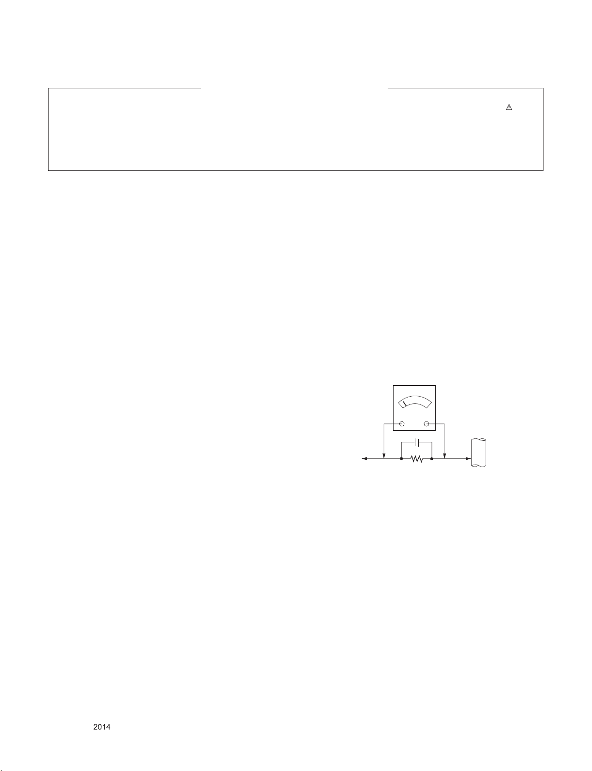
Leakage Current Hot Check (See below Figure)
Plug the AC cord directly into the AC outlet.
Do not use a line Isolation Transformer during this check.
Connect 1.5K/10watt resistor in parallel with a 0.15uF capacitor
between a known good earth ground (Water Pipe, Conduit, etc.)
and the exposed metallic parts.
Measure the AC voltage across the resistor using AC voltmeter
with 1000 ohms/volt or more sensitivity.
Reverse plug the AC cord into the AC outlet and repeat AC voltage
measurements for each exp ose d metallic par t. Any voltage
measured must not exceed 0.75 volt RMS which is corresponds to
0.5mA.
In case any measurement is out of the limits specified, there is
possibility of shock hazard and the set must be checked and
repaired before it is returned to the customer.
Leakage Current Hot Check circuit
Good Earth Ground
such as WATER PIPE,
To Instrument's
exposed
METALLIC PARTS
When 25A is impressed between Earth and 2nd Ground
for 1 second, Resistance must be less than 0.1
*Base on Adjustment standard
0.15µF
1.5 Kohm/10W
CONDUIT etc.
Copyright ©
Only for training and service purposes
LG Electronics. Inc. All right reserved.
- 3 -
LGE Internal Use Only
Page 4

SERVICING PRECAUTIONS
CAUTION: Before servicing receivers covered by this service
manual and its supplements and addenda, read and follow the
SAFETY PRECAUTIONS on page 3 of this publication.
NOTE: If unforeseen circumstances create conflict between the
following servicing precautions and any of the safety precautions on
page 3 of this publication, always follow the safety precautions.
Remember: Safety First.
General Servicing Precautions
1. Always unplug the receiver AC power cord from the AC power
source before;
a. Removing or reinstalling any component, circuit board
module or any other receiver assembly.
b. Disconnecting or reconnecting any receiver electrical plug or
other electrical connection.
c. Connecting a test substitute in parallel with an electrolytic
capacitor in the receiver.
CAUTION: A wrong part substitution or incorrect polarity
installation of electrolytic capacitors may result in an
explosion hazard.
2. Test high voltage only by measuring it with an appropriate high
voltage meter or other voltage measuring device (DVM,
FETVOM, etc) equipped with a suitable high voltage probe.
Do not test high voltage by "drawing an arc".
3. Do not spray chemicals on or near this receiver or any of its
assemblies.
4. Unl ess sp ecified othe rwise in this service manua l, clean
electrical contacts only by applying the following mixture to the
contacts with a pipe cleaner, cotton-tipped stick or comparable
non-abrasive applicator; 10% (by volume) Acetone and 90% (by
volume) isopropyl alcohol (90%-99% strength)
CAUTION: This is a flammable mixture.
Unless specified otherwise in this service manual, lubrication of
contacts in not required.
5. Do not defeat any plug/socket B+ voltage interlocks with which
receivers covered by this service manual might be equipped.
6. Do not apply AC power to this instrument and/or any of its
electrical assemblies unless all solid-state device heat sinks are
correctly installed.
7. Always connect the test receiver ground lead to the receiver
chassis ground before connecting the test receiver positive
lead.
Always remove the test receiver ground lead last.
8. Use with this receiver only the test fixtures specified in this
service manual.
CAUTION: Do not connect the test fixture ground strap to any
heat sink in this receiver.
Electrostatically Sensitive (ES) Devices
Some semiconductor (solid-state) devices can be damaged easily
by static electricity. Such components com monly are called
Electrostatically Sensitive (ES) Devices. Examples of typical ES
devices are integrated circuits and some field-effect transistors and
semiconductor "chip" compon ents. The following techniques
should be used to help reduce the incide nce of compon ent
damage caused by static by static electricity.
1. Immediately before handling any semiconductor component or
semiconductor-equipped assembly, drain off any electrostatic
charge on your body by touching a known earth ground.
Alter natively, obtain and wear a comme rcially availab le
discharging wrist strap device, which should be removed to
prevent potential shock reasons prior to applying power to the
unit under test.
2. After removing an el ectrical assembly equipped with ES
devices, place the assembly on a conductive surface such as
aluminum foil, to prevent electrostatic charge buildup or
exposure of the assembly.
3. Use only a grounded-tip soldering iron to solder or unsolder ES
devices.
4. Use only an anti-static type solder removal device. Some solder
removal devices not classified as "anti-static" can generate
electrical charges sufficient to damage ES devices.
5. Do not use freon-propelled chemicals. These can generate
electrical charges sufficient to damage ES devices.
6. Do not remove a replacement ES device from its protective
package until immediately before you are ready to install it.
(Most re pla cem ent ES dev ice s are packaged with leads
electrically shorted together by conductive foam, aluminum foil
or comparable conductive material).
7. Immediately before removing the protective material from the
leads of a replacement ES device, touch the protective material
to the chassis or circuit assembly into which the device will be
installed.
CAUTION: Be sure no power is applied to the chassis or circuit,
and observe all other safety precautions.
8. Mi nimiz e bodil y motions w hen h an dl ing u np ac kaged
replacement ES devices. (Otherwise harmless motion such as
the brushing together of your clothes fabric or the lifting of your
foot fro m a carp eted floor can ge ner ate st atic electricit y
sufficient to damage an ES device.)
General Soldering Guidelines
1. Use a grounded-tip, low-wattage soldering iron and appropriate
tip size and shape that will maintain tip temperature within the
range or 500 ˚F to 600 ˚F.
2. Use an appropriate gauge of RMA resin-core solder composed
of 60 parts tin/40 parts lead.
3. Keep the soldering iron tip clean and well tinned.
4. Thoroughly clean the surfaces to be soldered. Use a mall wirebristle (0.5 inch, or 1.25cm) brush with a metal handle.
Do not use freon-propelled spray-on cleaners.
5. Use the following unsoldering technique
a. Allow the soldering iron tip to reach normal temperature.
(500 ˚F to 600 ˚F)
b. Heat the component lead until the solder melts.
c. Quickly draw the melted solder with an anti-static, suction-
type solder removal device or with solder braid.
CAUTION: Work quickly to avoid overheating the circuit
board printed foil.
6. Use the following soldering technique.
a. Allow the soldering iron tip to reach a normal temperature
(500 ˚F to 600 ˚F)
b. First, hold the soldering iron tip and solder the strand against
the component lead until the solder melts.
c. Quickly move the soldering iron tip to the junction of the
component lead and the printed circuit foil, and hold it there
only un til the solder fl ows onto and around both the
component lead and the foil.
CAUTION: Work quickly to avoid overheating the circuit
board printed foil.
d. Closely inspect the solder area and remove any excess or
splashed solder with a small wire-bristle brush.
Copyright ©
Only for training and service purposes
LG Electronics. Inc. All right reserved.
- 4 -
LGE Internal Use Only
Page 5

IC Remove/Replacement
Some chassis circuit boards have slotted holes (oblong) through
which the IC leads are inserted and then bent flat against the
circuit foil. When holes are the slotted type, the following technique
should be used to remove and replace the IC. When working with
boards using the familiar round hole, use the standard technique
as outlined in paragraphs 5 and 6 above.
Removal
1. Desolder and straighten each IC lead in one operation by gently
prying up on the lead with the soldering iron tip as the solder
melts.
2. Draw away the melted solder with an anti-static suction-type
solder removal device (or with solder braid) before removing the
IC.
Replacement
1. Carefully insert the replacement IC in the circuit board.
2. Carefully bend each IC lead against the circuit foil pad and
solder it.
3. Clean the soldered areas with a small wire-bristle brush.
(It is not necessary to reapply acrylic coating to the areas).
"Small-Signal" Discrete Transistor
Removal/Replacement
1. Remove the defective transistor by clipping its leads as close as
possible to the component body.
2. Bend into a "U" shape the end of each of three leads remaining
on the circuit board.
3. Bend into a "U" shape the replacement transistor leads.
4. Connect the replacement transistor leads to the corresponding
leads extending from the circuit board and crimp the "U" with
long nose pliers to insure metal to metal contact then solder
each connection.
CAUTION: Maintain original spacing between the replaced
component and adjacent components and the circuit board to
prevent excessive component temperatures.
Circuit Board Foil Repair
Excessive heat applied to the copper foil of any printed circuit
board will weaken the adhesive that bonds the foil to the circuit
board causing the foil to separate from or "lift-off" the board. The
following guidelines and procedures should be followed whenever
this condition is encountered.
At IC Connections
To repair a defective copper pattern at IC connections use the
following procedure to install a jumper wire on the copper pattern
si de of the circuit board. (Use this techniq ue onl y on IC
connections).
1. Carefully remove the damaged copper pattern with a sharp
knife. (Remove only as much copper as absolutely necessary).
2. carefully scratch away the solder resist and acrylic coating (if
used) from the end of the remaining copper pattern.
3. Bend a small "U" in one end of a small gauge jumper wire and
carefully crimp it around the IC pin. Solder the IC connection.
4. Route the jumper wire along the path of the out-away copper
pattern and let it overlap the previously scraped end of the good
copper pattern. Solder the overlapped area and clip off any
excess jumper wire.
At Other Connections
Use the following technique to repair the defective copper pattern
at connections other than IC Pins. This technique involves the
installation of a jumper wire on the component side of the circuit
board.
Power Output, Transistor Device
Removal/Replacement
1. Heat and remove all solder from around the transistor leads.
2. Remove the heat sink mounting screw (if so equipped).
3. Carefully remove the transistor from the heat sink of the circuit
board.
4. Insert new transistor in the circuit board.
5. Solder each transistor lead, and clip off excess lead.
6. Replace heat sink.
Diode Removal/Replacement
1. Remove defective diode by clipping its leads as close as
possible to diode body.
2. Bend the two remaining leads perpendicular y to the circuit
board.
3. Observing diode polarity, wrap each lead of the new diode
around the corresponding lead on the circuit board.
4. Securely crimp each connection and solder it.
5. Inspect (on the circuit board copper side) the solder joints of
the two "original" leads. If they are not shiny, reheat them and if
necessary, apply additional solder.
Fuse and Conventional Resistor
Removal/Replacement
1. Clip each fuse or resistor lead at top of the circuit board hollow
stake.
2. Securely crimp the leads of replacement component around
notch at stake top.
3. Solder the connections.
1. Remove the defective copper pattern with a sharp knife.
Remove at least 1/4 inch of copper, to ensure that a hazardous
condition will not exist if the jumper wire opens.
2. Trace along the copper pattern from both sides of the pattern
break an d loc ate the nearest component that is dir ect ly
connected to the affected copper pattern.
3. Connect insulated 20-gauge jumper wire from the lead of the
nearest component on one side of the pattern break to the lead
of the nearest component on the other side.
Carefully crimp and solder the connections.
CAUTION: Be sure the insulated jumper wire is dressed so the
it does not touch components or sharp edges.
Copyright ©
Only for training and service purposes
LG Electronics. Inc. All right reserved.
- 5 -
LGE Internal Use Only
Page 6
SPECIFICATION
NOTE : Specications and others are subject to change without notice for improvement.
1. Application Range
This spec sheet is applied all of the TV used LU40A chassis.
2. Specication
Each part is tested as below without special appointment
1) Temperature : 25 ˚C ± 5 ˚C (77 ˚F ± 9 ˚F),
CST : 40 ˚C ± 5 ˚C
2) Relative Humidity : 65 % ± 10 %
3) Power Voltage : Standard input voltage
(100 V - 240 V ~, 50 / 60 Hz)
· Standard Voltage of each products is marked by models
4) Specication and performance of each parts are followed
each drawing and specication by part number in accord-
ance with BOM.
5) The receiver must be operated for about 5 minutes prior to
the adjustment.
3.Test method
1) Performance : LGE TV test method followed
2) Demanded other specication
- Safety : CE,IEC specication
- EMC : CE,IEC specication
4. General specication
4.1. TV
No Item Specication Remarks
1 Market AMERICA, CANADA, MEXICO
2 Available Channel 1)Digital : ATSC
2)Analog : NTSC
3 Receiving system ATSC / NTSC-M
4 Interface RF / Composite(CVBS) / Component / HDMI(1EA)
/ USB / RS-232 (SVC only)
4.2. Feature and Function
No Item Specication Remarks
1 RF Input Analog NTSC
DTV ATSC
2 HDMI Input (Rear) HDMI version 1.4/ support PC
Support HDCP
3 Component Input
(Rear, 1EA)
4 CVBS Input ATSC/NTSC-M common port with Component.
5 USB (Side, 1EA) For My Media(Photo/Music List) Picture + Music
6 RS-232C(Side, 1EA) SVC only
Y/Pb/Pr
Rear : 1EA
Copyright © LG Electronics. Inc. All right reserved.
Only for training and service purposes
- 6 -
LGE Internal Use Only
Page 7
4.3. HDMI(PC) Specication
No Item Specication Remarks
1 Supported Sync. Type Separate Sync., Digital
2 Operating Frequency Analog Horizontal 30 ~ 83 kHz
Vertical 60 Hz
Digital Horizontal 30 ~ 83 kHz
Vertical 56 ~ 75 Hz
3 Resolution Analog Max. 1920 x 1080 @ 60 Hz
Recommend 1920 x 1080 @ 60 Hz
Digital Max. 1920 x 1080 @ 60 Hz
Recommend 1920 x 1080 @ 60 Hz
5. External Input Support Format
- HDMI (PC)
No. Resolution H-freq(kHz) V-freq(Hz) Pixel clock(MHz) Remark
1 720*400 31.468 70.080 28.321
2 640*480 31.469 59.940 25.175
3 640*480 37.500 75.000 31.500
4 800*600 37.879 60.317 40.000
5 800*600 46.875 75.000 49.500
6 1024*768 48.363 60.004 65.000
7 1024*768 60.023 75.029 78.750
8 1280*800 49.702 59.810 83.500
9 1366*768 47.717 59.79 85.5
- HDMI (DTV)
No. Resolution H-freq(kHz) V-freq(Hz) Pixel clock(MHz) Remark
1 720* 480 31.469 / 31.5 59.94 / 60 27.00/ 27.03 SDTV 480P
2 720*576 31.25 50.00 27.864 SDTV 576P
3 1280*720 37.50 50.00 74.250 HDTV 720P
4 1280* 720 44.96 / 45 59.94 / 60 74.17/ 74.25 HDTV 720P
5 1920* 1080 33.72 / 33.75 59.94 / 60 74.17/ 74.25 HDTV 1080I
6 1920* 1080 28.125 50.00 74.25 HDTV 1080I
7 1920* 1080 27.00 24 74.25 HDTV 1080P
8 1920* 1080 33.75 30.00 74.25 HDTV 1080P
9 1920* 1080 56.250 50 148.5 HDTV 1080P
10 1920* 1080 67.43 / 67.5 59.94 / 60 148.35/ 148.50 HDTV 1080P
Copyright © LG Electronics. Inc. All right reserved.
Only for training and service purposes
- 7 -
LGE Internal Use Only
Page 8
- Component
No
1 720x480 15.73 59.94 720x480i
2 15.73 60
3 720x480 31.47 59.94 720x480p
4 31.5 60
5 1280x720 44.96 59.94 1280x720p
6 45 60
7 1920x1080 33.72 59.94 1920x1080i
8 33.75 60
9 26.97 23.976 1920x1080p
10 27 24
11 33.71 29.97
12 33.75 30
13 67.432 59.94
14 67.5 60
Resolution H-freq(kHz) V-freq(Hz)
Specication
Remark
Copyright ©
Only for training and service purposes
LG Electronics. Inc. All right reserved.
- 8 -
LGE Internal Use Only
Page 9
ADJUSTMENT INSTRUCTION
(6)
(2)
1. Application Range
This document is applied to LU40A chassis TV which is manufactured in TV (or Monitor) Factory or is produced on the basis
of this data.
2. Designation
1) The adjustment is according to the order which is designat-
ed and which must be followed, according to the plan which
can be changed only on agreeing.
2) Power adjustment : Free Voltage.
3) Magnetic Field Condition: Nil.
4) Input signal Unit: Product Specication Standard.
5) Reserve after operation: Above 5 Minutes (Heat Run)
Temperature : at 25 °C ± 5 °C
Relative humidity : 65 % ± 10 %
Input voltage : 220 V, 60 Hz
6) Adjustment equipments : Color Analyzer (CA-210 or CA-
110), DDC Adjustment Jig equipment, SVC remote controller.
7) Push The "IN STOP KEY" – For memory initialization
Case1 : Software version up
1) After downloading S/W by USB , Multi-vision set will
reboot automatically
2) Push "In-stop" key
3) Push "Power on" key
4) Function inspection
5) After function inspection, Push "In-stop" key.
Case2 : Function check at the assembly line
1) When TV set is entering on the assembly line, Push "In-
stop" ke y at rst.
2) Push "Power on" key for turning it on.
→ If you push "Power on" key, TV set will recover channel
information by itself.
3) After function inspection, Push "In-stop" key.
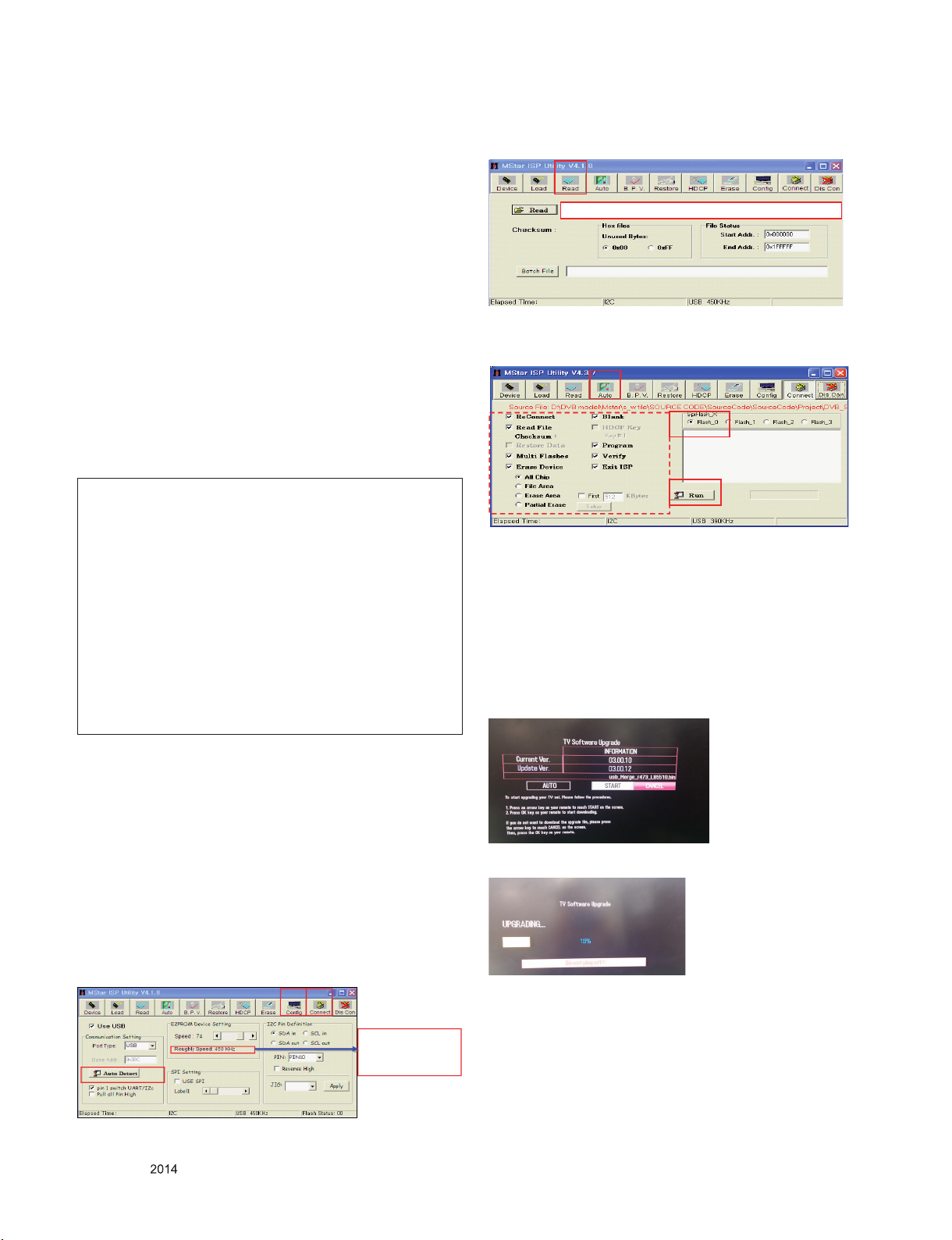
4) Click “Read” tab, and then load download le(XXXX.bin) by
clicking “Read”
(4)
filexxx.bin
5) Click “Auto” tab and set as below
6) Click “Run”.
7) After downloading, check “OK” message.
(5)
(5)
(7) ……….OK
* USB DOWNLOAD
1) Make New folder named “LG_DTV” and USB download le
in the folder.
2) Put the USB storage to the USB socket.
3) Automatically detecting update le in USB Stick
- If your downloaded program version in USB Stick is
Low, it didn’t work. But your downloaded version is
High, USB data is automatically detecting.
4) TV Software Upgrade feature will be displayed.
3. Main PCB check process
* APC - After Manual-Insult, executing APC
* Connect DFT jig during Main PCB check process.
* Boot le Download
1) Execute ISP program “Mstar ISP Utility” and then click
“Cong” tab.
2) Set as below, and then click “Auto Detect” and check “OK”
message. If display “Error”, Check connect computer, jig,
and set.
3) Click “Connect” tab. If display “Can’t ”, Check connect
computer, jig, and set.
(1) (3)
Please Check the Speed :
Use the speed under
OK
Copyright ©
Only for training and service purposes
LG Electronics. Inc. All right reserved.
200KHz.
5) Updating is starting.
6) Updating Completed, The TV will restart automatically.
7) If your TV is turned on, check your updated version and
Tool option. (refer to next page tool option section)
* If downloading version is higher than your TV have, TV
can lost all channel data. In this case, you have to channel
recover. if all channel data is cleared, you didn’t have a DTV/
ATV test on production line.
* After downloading, have to adjust TOOL OPTION again.
- 9 -
LGE Internal Use Only
Page 10

3.1. EDID Process
3.1.1. EDID download
1) Press “Power only” key of service remote controller.
2) Press the “ADJ” Key of service remote controller.
3) Enter EDID D/L mode by pushing “►” key at “EDID D/L”.
4) Select “Start” menu to download EDID data.
5) Check the “OK” message.
6) Press EXIT key on R/C.
→ Caution: Do not connect HDMI Cable when download
EDID
* Edid data and Model option download (RS232)
NO Item CMD 1CMD 2Data 0
3.2. Function Check
3.2.1. Check display and sound
*Check Input and Signal items. (cf. work instructions)
1) TV
2) AV (CVBS)
3) COMPONENT (480i)
4) HDMI
* Display and Sound check is executed by Remote controller.
→ Caution : Not to push the INSTOP KEY after completion if
the function inspection.
Enter
download
MODE
EDID data and
Model option
download
Download
‘Mode In’
Download A E 00 10 Automatically download
A A 0 0 When transfer the
→ Caution
* Use the proper signal cable for EDID Download
- Analog EDID : Pin3 exists
- Digital EDID : Pin3 exists
3.1.2. EDID Data
- HDMI : Checksum : 98 FO
‘Mode In’,
Carry the command.
(The use of a internal
Data)
Copyright ©
LG Electronics. Inc. All right reserved.
Only for training and service purposes
- 10 -
LGE Internal Use Only
Page 11

4. Total Assembly line process
Color Analyzer
Computer
Pattern Generator
※
※If TV internal pattern is used, not needed
Signal So urce
Probe
RS-232C
RS-232C
RS-232C
DFT JIG
RGB Cable
*Connection
4.1. Tool option & ADC Check
1) Press "Power on" key of service remote control.
2) Connect audio signal cable to phone jack for RS232.
3) Check the 'Tool Option' (Refer to the BOM Comments or
Adjustment spec)
4) Check the ‘ADC’ is ok.
4.2. Model name & Serial number Download
4.2.1. Model name & Serial number D/L
1) Press "Power on" key of service remote control.
2) Connect RS232 Signal Cable to RS-232 Jack.
3) Write Serial number by use RS-232.
4) Must check the serial number at the Diagnostics of SET UP
menu. (Refer to below).
4.2.2. Method & notice
1) Model Name & Serial Number D/L is using of scan equipment.
2) Setting of scan equipment operated by Manufacturing
Technology Group.
3) Serial number D/L must be conformed when it is produced
in production line, because serial number D/L is mandatory
by D-book 4.0
4) Check the model name Instart menu → Factory name
displayed (ex 24LN4500)
5) Check the Diagnostics (DTV country only) → Buyer model
displayed (ex 24LN4500)
4.4. White balance adjustment
-Equipment
1) Color Analyzer: CA-210 (LED Module : CH 14)
2) Adj. Computer(During auto adj., RS-232C protocol is
needed)
3) Adjust Remocon
RGB_Gains are xed data for each model.
Insert RS-232C Jack which is connected with PC for White
Balance or equivalent device.
* Total Assembly line should be check whether the color
coordinate(x,y) data refer to below table were meet or not.
Color coordinate is differ from panel’s characteristics of color
temperature. Please check panel characteristics about color
temperature.
-Cool Panel
Color
Temperature
Luminance
(cd/m²)
*Note : x,y coordinates are drifted about 0.007 after 30 mins
Cool 13,000 °K X=0.276 (±0.04)
Medium 9,300k °K X=0.290 (±0.04)
Warm 6,500k °K X=0.318 (±0.04)
Cool Min : 80 Typ : 110 <Test Signal>
Medium Min : 80 Typ : 110
Warm Min : 70 Typ : 110
Y=0.275 (±0.04)
Y=0.298 (±0.04)
Y=0.334 (±0.04)
<Test Signal>
Inner pattern
(204gray,80IRE)
Inner pattern
(204gray,80IRE)
heat-run. So checking color coordinate within 5-min at
total assembly line, consider x,y coordinates might be
up to 0.007 than x,y target of each color temperature.
4.3. Function Check
4.3.1. Check display and sound
*Check Input and Signal items. (cf. work instructions)
1) TV
2) AV (CVBS)
3) COMPONENT (480i)
4) HDMI
* Display and Sound check is executed by Remote controller.
→ Caution : Not to push the INSTOP KEY after completion if
the function inspection.
Copyright ©
Only for training and service purposes
LG Electronics. Inc. All right reserved.
- 11 -
LGE Internal Use Only
Page 12

*Auto-control interface and directions
1) Adjust in the place where the inux of light like oodlight
around is blocked. (Illumination is less than 10ux).
2) Adhere closely the Color Analyzer ( CA210 ) to the module
less than 10cm distance, keep it with the surface of the
Module and Color Analyzer’s Prove vertically.(80~100°).
3) Aging time
- After aging start, keep the power on (no suspension of
power supply) and heat-run over 5 minutes.
- Using ‘no signal’ or ‘full white pattern’ or the others,
check the back light on.
* Auto adjustment Map(RS-232C)
RS-232C COMMAND
[ CMD ID DATA ]
Wb 00 00 White Balance Start
Wb 00 ff White Balance End
RS-232C COMMAND
[CMD ID DATA]
Cool Mid Warm Cool Mid Warm
R Gain jg Ja jd 00 172 192 192 192
G Gain jh Jb je 00 172 192 192 192
B Gain ji Jc jf 00 192 192 172 192
R Cut 64 64 64 128
G Cut 64 64 64 128
B Cut 64 64 64 128
MIN CENTER
(DEFAULT)
4.5. Model Name & SW Version & Adjust
check.
* Press the ‘Instart’ key of ADJ remote controller
4.5.1. Model Name& SW Version Check
1) Check ‘Model Name’.
2) Check ‘S/W Version’ (Refer to the IC Ver. in the BOM)
4.5.2. Adjust Check
1) Check ‘Country Group’
2) Check ‘Area Option’
3) Check ‘Tool Option’ (Refer to the BOM Comments)
4) Check ‘EDID[RGB&HDMI]’ is OK.
* After check all, Press the 'EXIT' key of ADJ remote controller
to go out SVC menu.
MAX
** Caution **
Color Temperature : COOL, Medium, Warm.
One of R Gain/G Gain/ B Gain should be kept on 0xC0, and
adjust other two lower than C0.
(when R/G/B Gain are all C0, it is the FULL Dynamic Range
of Module)
*Note : Manual W/B process using adjusts Remote control.
1) After enter Service Mode by pushing "ADJ" key,
2) Enter "White Balance" by pushing "►" key at "White Bal-
ance".
* When doing Adjustment, Please make circumstance as
below.
4.6. Outgoing condition Conguration
* After all function test., press IN-STOP Key by SVC Remote
controller. And make Outgoing Condition
Copyright ©
Only for training and service purposes
LG Electronics. Inc. All right reserved.
- 12 -
LGE Internal Use Only
Page 13

1. No Power
Replace X300
N
Check C500
Voltage Level (19V)
Check Power connector
OK ?
Replace Adapter
Y
N Y
Check IC501 Output
Voltage Level (3.3V)
Replace IC501 &
Recheck
Y
N
Check X300 Clock
24MHz
Replace IC405 Flash
Memory
Y
Check IC503 Output
Voltage Level (5V)
Replace IC503 &
Recheck
Y
N
Check IC502 Output
Voltage Level (1.15V)
Replace IC502 &
Recheck
N
Y
TROUBLE SHOOTING
Copyright ©
Only for training and service purposes
LG Electronics. Inc. All right reserved.
- 13 -
LGE Internal Use Only
Page 14

2. No Picture
Replace Cable
N
Module Back Light On?
Check IC700 & Q700
Replace LED Driver IC or FET
Y
N
N
Check Panel Power 12V (P401
#30)
Check IC500 Output 12V
Replace IC500 &
Recheck
Y
N
Check Panel input Clock
P401 (#9, #10 )
Check IC300
Repair Main B/D
Y
N
Check FFC Cable for Damage or
Open Conductors
Check LED Driver Output
(C706)
Replace T-Con Board or Module
Y
Check IC300
Replace Main SOC
N
Check WLED_ENABLE High?
Y
Copyright ©
Only for training and service purposes
LG Electronics. Inc. All right reserved.
- 14 -
LGE Internal Use Only
Page 15

3. No Video - Digital TV
Check RF Cable
Y
1. Check RF IC(L200) Power (3.3V)
2. Check IC501 Output voltage(3.3V)
Replace IC501 &
Recheck
Y
N
Check SCL/SDA Line(TU200 #3, #4)
Replace TU200 or
IC300(=> Main Scaler)
N
Copyright ©
Only for training and service purposes
LG Electronics. Inc. All right reserved.
- 15 -
LGE Internal Use Only
Page 16

4. No Video - HDMI
Replace Main Scaler
(IC300)
Check input signal format
Is it supported?
Check JK100 for proper
connection or Damage
Replace Connector
Y
N
Check I2C Signal
(JK100)
Re Download EDID Data
Y
N
Y
Check HDMI Cable for Damage or
Open Connector
Y
Copyright ©
LG Electronics. Inc. All right reserved.
Only for training and service purposes
- 16 -
LGE Internal Use Only
Page 17

BLOCK DIAGRAM
Copyright ©
Only for training and service purposes
LG Electronics. Inc. All right reserved.
- 17 -
LGE Internal Use Only
Page 18

EXPLODED VIEW
IMPORTANT SAFETY NOTICE
Many electrical and mechanical parts in this chassis have special safety-related characteristics. These parts
are identified by in the Schematic Diagram and EXPLODED VIEW.
It is essential that these special safety parts should be replaced with the same components as recommended
in this manual to prevent X-RADIATION, Shock, Fire, or other Hazards.
Do not modify the original design without permission of manufacturer.
910
400
900
535
LV1
A2
200
300
540
510
120
820
800
810
Copyright © LG Electronics. Inc. All right reserved.
Only for training and service purposes
- 18 -
LGE Internal Use Only
Page 19

<HDMI 2>
Copyright ⓒ 2014 LG Electronics. Inc. All right reserved.
Only for training and service purposes
LGE Internal Use Only
SHIELD
20
19
18
17
16
15
14
13
12
11
CK+
10
EAG61491201
D0-
9
D0_GND
8
D0+
7
D1-
6
D1_GND
5
D1+
4
D2-
3
D2_GND
2
D2+
1
JK100
COMPONENT
6A
[GN/YL]E-LUG
5A
[GN/YL]O-SPRING
4A
[GN/YL]CONTACT
5B
[BL]O-SPRING
7C
[RD1]E-LUG-S
5C
[RD1]O-SPRING
4C
[RD1]CONTACT
5D
[WH]O-SPRING
4E
[RD2]CONTACT
5E
[RD2]O-SPRING
6E
PPJ245N2-01
[RD2]E-LUG
JK101
5V_HDMI_1
R100
1K
120825
ESD component addition
OPT
VA100
20V
+3.3V_ST
R101
OPT
VA101
5.6V
OPT
VA102
20V
47K
VA103
20V
R103
47K
C
R102
10K
B
Q100
MMBT3904(NXP)
E
OPT
MMBT3904(NXP)
CEC_REMOTE
(OPT)ESD_HDMI_SEMTECH(DEV)
D100
RCLAMP0524PA
1
10
9
8
7
6
10
9
8
7
6
CK-_HDMI1
CK+_HDMI1
D0-_HDMI1
D0+_HDMI1
D1-_HDMI1
D1+_HDMI1
D2-_HDMI1
D2+_HDMI1
ZD104-*1
(OPT)ESD_COMP_ZENER_KEC
ZD105-*1
(OPT)ESD_COMP_ZENER_KEC
2
3
4
5
(OPT)ESD_HDMI_SEMTECH(DEV)
D101
RCLAMP0524PA
1
2
3
4
5
ESD_COMP_ZENER_KEC
ZD105
ESD_COMP_ZENER_KEC
OPT
VA105
5.6V
ZD101
ZD103
VA107
5.6V
OPT
VA122
5.6V
OPT
47K
R104
5.6B
ZD104
5.6B
5.6B
ZD100
5.6B
5.6B
ZD102
5.6B
5V_DET_HDMI_1
C
Q101
E
120715
Added for ESD prevention
120825
OPT->APPLY
R10 6
75
1%
R10 7
C100
1000pF
50V
C101
1000pF
50V
Headphone block
+3.3V
+INR
-INR
OUTR
GND_1
MUTE
HP OUT
IC101
TPA6138A2
C113
1uF
10V
+INL
14
-INL
13
OUTL
12
UVP
11
GND_2
10
VDD
9
CP
8
C114
10pF
50V
HP OUT
R135
43K
HP OUT
C115
1uF
10V
1%
HP OUT
1
2
3
4
5
VSS
6
CN
7
+3.3V
L102
120-ohm
BLM18PG121SN1D
C116
180pF
50V
R136
33K
HP OUT
HP OUT
HP OUT
C117
0.1uF
16V
R137
10K
HP OUT
HP_LOUT
HP OUT
1uF
10V
C118
HP OUT
HP_LOUT_PWM
HP OUT
VA124
R140
20V
100
MNT_USE
R189 0
R126 100
R190
MNT_USE
P100
1
2
3
4
5
0
JackShield(for NonCKD)
M1
MGJ63348201
+3.3V_ST
VA125
VCC
OPT_Event debug
16
GND
15
DOU T1
14
RIN 1
13
ROU T1
12
DIN 1
11
DIN2
10
ROUT2
9
IC102
MAX3232CDR
20V
PM_TXD
PM_RXD
1
2
3
4
5
6
7
8
JackShield(for CKD)
M1-*1
MGJ63348202
OPT_RS232C_VA
OPT_RS232C_VA
VA126
20V
+3.3V_ST
C1+
C123
0.1uF
V+
16V
C120
0.1uF
C1-
16V
OPT_Event debug
C2+
OPT_Event debug
C121
0.1uF
C2-
16V
V-
DOUT2
RIN2
OPT_Event debug
C122
0.1uF
16V
OPT_Event debug
C124
0.1uF
16V
OPT_Event debug
+5V
5V_HDMI_1
A2CA1
MMBD6100
D104
HP OUT
R121
2.7K
120915
47K->2.7K
R120
2.7K
DDC_SDA_1
OPT
R110
10K
B
HPD1
DDC_SDA_1
R119
0
CEC
DDC_SCL_1
CEC_REMOTE
KJA-PH-1-0177-2
6 M6
1 M1
3 M3_DETECT
4 M4
5 M5_GND
JK102
DDC_SCL_1
VA109
VA108
20V
20V
TMDS_CH1-
TMDS_CH1+
TMDS_CH2-
TMDS_CH2+
IP4283CZ10-TBA
1
2
GND_1
3
4
5
ESD_HDMI_NXP
D100-*1
10
D101-*1
IP4283CZ10-TBA
GND_1
1
2
3
4
5
ESD_HDMI_NXP
NC_4
10
NC_3
9
GND_2
8
NC_2
7
NC_1
6
<DSUB_RGB>
121128
ESD improve
2:E18
2:E18
OPT->APPLY
DSUB_VSYNC
DSUB_HSYNC
NC_4
TMDS_CH1-
NC_3
TMDS_CH1+
9
GND_2
8
NC_2
TMDS_CH2-
7
TMDS_CH2+
NC_1
6
DSUB_B+
DSUB_G+
DSUB_R+
11.10.31
To Improve EMI
AV_DET
COMP_Y+
<USB_SIDE>
R105
75
1%
R116
+3.3V
10K
R118
1K
OPT
C102
0.1uF
16V
COMP_Pb+
+3.3V
C104
R115
10K
R117
1K
VA106
5.6V
OPT
75
1%
R111
R108
470K
OPT
R109
470K
OPT
10K
R112
10K
R114
12K
R113
12K
COMP_DET
COMP_Pr+
COMP_L_IN
COMP_R_IN
3AU04S-305-ZC-(LG)
JK103
1234
USB DOWN STR EAM
5
0.1uF
JP113
JP112
JP111
16V
OPT
C107
22uF
6.3V
VA110
121128
ESD improve
OPT->APPLY
75
20V
R144
JP116
D_SUB
D_SUB
R145
75
HP OUT
R122
47K
JP107
JP109
JP108
R146 0
121128
ESD improve
OPT->APPLY
VA104
JP110
HP OUT
HP OUT
VA114
20V
D_SUB
R147
0
D_SUB
D_SUB
R148
75
D_SUB
To Improve Ringing issue
LOW capacitance Part apply
IC100
AP2191DSG
NC
8
1
OUT_2
2
7
OUT_1
3
6
FLG
4
5
VA111
20V
JP128
HP OUT
R123
1K
VA112
20V
HP OUT
20V
D_SUB
VA115
20V
D_SUB
R149
0
VA116
11.10.27
D_SUB
D_SUB
D_SUB
GND
IN_1
IN_2
EN
SIDE_USB_DM
SIDE_USB_DP
111026
ESD diode deletion
EAH39491601 2EA
120103
ESD diode addition
EAF61530301 2EA
JP129 JP130
BLM18AG151SN1D
VA113
20V
HP OUT
121128
ESD improve
OPT->APPLY
5.5V
VA117
USB1_CTL
HP_DET
HP OUT
L100
C103
0.22uF
16V
5.5V
VA118
JP119
JP120
R131
10K
5.5V
R132
47
HP_ROUT
L101
BLM18AG151SN1D
HP OUT
SB_MUTE
C106
0.22uF
HP_MUTE
16V
HP OUT
MNT_USE
R150
10K
VA119
D_SUB
121128
ESD improve
OPT->APPLY
JP123
JP121
JP122
+5V
C105
0.1uF
16V
USB1_OCD
HP_LOUT
HP OUT
MMBD6100
A2
A1
MNT_USE
D103
MMBD6100
A2
C
A1
MNT_USE
R151
10K
20V
JP124
H_SYN C
DDC_D ATA
GND_2
BLUE_ GND
RED2GREEN3BLUE4GND_15DDC_G ND
GREEN _GND
RED_G ND
12
11
8
7
6
1
JK105
SPG09-DB-010
D_SUB
D102
NC
13
9
HP_ROUT_PWM
R124
C
10K
HP OUT
121128
ESD improve
OPT->APPLY
JP125
DDC_C LOCK
V_SYN C
SYNC_ GND
15
14
10
HP OUT
C108
1uF
10V
HP OUT
HP_ROUT
+3.3V
HP OUT
R127
10K
C
Q102
B
MMBT3904(NXP)
E
HP OUT
+5V
D_SUB
+3.3V_ST
VA120
20V
VA121
20V
D_SUB
121128
ESD improve
OPT->APPLY
JP126
SHILE D
16
<RS232C>
R129
10K
HP OUT
HP OUT
R152
47K
R130
R128
33K
D_SUB
D_SUB
R153
10K
JK104
C109
180pF
R133
HP OUT
50V
33K
100
R154
47K
B
6 M6
1 M1
3 M3_DETECT
4 M4
5 M5_GND
HP OUT
HP OUT
R134
43K
C112
1%
10pF
50V
HP OUT
C110
C111
1000pF
1uF
50V
10V
HP OUT
HP OUT
PM_RXD
PM_TXD
D_SUB
DSUB_DET
C
Q103
MMBT3904(NXP)
D_SUB
E
Jack Shield (HDMI1, HDMI2, RGB)
VA123
20V
THE SYMBOL MARK OF THIS SCHEMETIC DIAGRAM INCORPORATES
SPECIAL FEATURES IMPORTANT FOR PROTECTION FROM X-RADIATION.
FIRE AND ELECTRICAL SHOCK HAZARDS, WHEN SERVICING IF IS
ESSENTIAL THAT ONLY MANUFACTURES SPECIFIED PARTS BE USED FOR
THE CRITICAL COMPONENTS IN THE SYMBOL MARK OF THE SCHEMETIC.
M1L
JACK INTERFACE
2013-07-13
1
7
Page 20

TUNER
Copyright ⓒ 2014 LG Electronics. Inc. All right reserved.
Only for training and service purposes
LGE Internal Use Only
KR/US(WO AD)
TU200
TDSS-H701F
1
2
3
4
5
6
7
8
9
10
11
NC_1
NC_2
SCL
SDA
+B1[3.3V]
NC_3
NC_4
NC_5
IF_AGC
DIF[P]
DIF[N]
R202
R203 33
+3.3V_TU
R207
1.8K
R204 33
R205 33
C204
18pF
50V
33
C206
18pF
50V
130118
option DEL
close to the tuner pin, add,09029
OPT
C208
20pF
50V
121118
SS BEAD->SUNLORD BEAD
C211
100pF
50V
L200
OPT
C209
20pF
50V
120OHM
R208
1.8K
C212
0.1uF
16V
TU_SCL
TU_SDA
+3.3V_TU
C214
100uF
16V
105C
OPT
B1
B1
12
SHIELD
A1
A1
Close to the tuner
C207
0.1uF
16V
R206 1K
should be guarded by ground
DIF_P
DIF_N
1. should be guarded by ground
2. No via on both of them
3. Signal Width >= 12mils
Signal to Signal Width = 12mils
Ground Width >= 24mils
IF_AGC
+3.3V_TU
60mA
OPT
C255
47uF
6.3V
85C
C210
22uF
6.3V
L203
UBW2012-121F
C213
0.1uF
16V
THE SYMBOL MARK OF THIS SCHEMETIC DIAGRAM INCORPORATES
SPECIAL FEATURES IMPORTANT FOR PROTECTION FROM X-RADIATION.
FIRE AND ELECTRICAL SHOCK HAZARDS, WHEN SERVICING IF IS
ESSENTIAL THAT ONLY MANUFACTURES SPECIFIED PARTS BE USED FOR
THE CRITICAL COMPONENTS IN THE SYMBOL MARK OF THE SCHEMETIC.
TUNER
+3.3V
C215
22uF
6.3V
C217
0.1uF
16V
M1L
Tuner block
2013-07-13
2
7
Page 21

+3.3V
Copyright ⓒ 2014 LG Electronics. Inc. All right reserved.
Only for training and service purposes
LGE Internal Use Only
TOUCH KEY
TOUCH KEY
R334
4.7K
R335
4.7K
R302
4.7K
R306
4.7K
<SOC_RESET>
+3.3V_ST
C300
10uF
10V
D400
MMBD6100
OPT
SB_MUTE
A2CA1
R303
100K
<HW_OPT>
+3.3V_ST
R348
1K
Not 19.5"
1K
R349
19.5"_1600*900
PIN NAME
MODEL_OPT_2
+3.3V_ST
R304
1K
FHD
HD
1K
R305
PIN NAME
MODEL_OPT_1
<VDDC 1.15V>
+1.15V_VDDC
10uF
C302
+3.3V_ST
R308
R309
4.7K
4.7K
R307
22
C305
0.1uF
16V
MODEL_OPT_2
MODEL OPTION
LOW
19.5"
MODEL_OPT
MODEL OPTION
LOW
FHD
10V
10V
C304 1uF
SOC_RESET
HIGH
Not used
HIGH
HD
0.1uF
16V
C306
0.1uF
C307
I2C_SDA
I2C_SCL
P_AMP_SDA
P_AMP_SCL
KEY_SDA
KEY_SCL
0.1uF
16V
16V
C308
0.1uF
C310
16V
DISP_EN
AVDD_MOD
KEY1
KEY2
5V_DET_HDMI_2
+1.15V_VDDC
DDR_DATA
MODEL_OPT
KEY_SCL
KEY_SDA
DDC_SCL_1
DDC_SDA_1
AV_DET
DDC_SDA_2
DDC_SCL_2
HPD2
TP302
+1.15V_VDDC
R300
10K
MMBT3904(NXP)
MHL_DET/GPIO86
CK-_HDMI2
CK+_HDMI2
D0-_HDMI2
D0+_HDMI2
+5V
R311
10K
Q300
C
B
E
R301
4.7K
AVDD_MOD_4
SAR0/GPIO75
SAR1/GPIO74
SAR2/GPIO73
VDDIO_DATA
DDCDD_CL
DDCDD_DA
DDCDA_CL
DDCDA_DA
DDCDB_DA
DDCDB_CL
HOTPLUG_B
AVDD_5V_MHL
GND_EFUSE
WLED_ENABLE
R347
20K
1/16W
1%
DM_P1
DP_P1
VDDC_3
GPIO54
VDDC_4
RXCN_D
RXCP_D
RX0N_D
RX0P_D
RX1N_D
RX1P_D
RX2N_D
RX2P_D
RXCN_B
RXCP_B
RX0N_B
RX0P_B
E-PAD
125
126
127
128
129
130
131
132
133
134
135
136
137
138
139
140
141
142
143
144
145
146
147
148
149
150
151
152
153
154
155
156
SIDE_USB_DM
SIDE_USB_DP
DM_P0
DP_P0
123
124
1
IR
SOC_RESET
RESET
122
MODEL_OPT_2
LED_AMBER
CEC
IRIN
INT/GPIO64/I2S_OUT_MCK
119
120
121
DDCA_CK
TEST
117
118
PM_TXD
PM_RXD
Don’t use arc/gpio87 as GPIO
ARC/GPIO87
DDCA_DA
116
157
THERMAL
5
6
TP301
33
R317
SPI_CK
114
115
SPI_SCK
/SPI_CS
R318 33
SPI_CZ
113
SPI_SDI
SPI_SDO
R319 33
R320 33
PWM0/GPIO15
SPI_DO
SPI_DI
111
112
HPD1
AMP_MUTE
PWM1
PWM0
HOTPLUG_D
HOTPLUG_A
PWM1/GPIO14
107
108
109
110
AMP_RESET_N
I2C_SCL
GPIO0/TCON0
106
LED_RED
I2C_SDA
GPIO4/TCON4
GPIO3/TCON3
GPIO2/TCON2
GPIO1/TCON1
103
104
105
POWER_ON/OFF1
DISP_EN
R324
R326
22
100
GPIO5/TCON5
101
102
MULTI_ON
/FLASH_WP
PANEL_CTL
GPIO6/TCON6
100
TU_SCL
GPIO9/TCON9
GPIO8/TCON8
GPIO7/TCON7
97
98
99
IC300
LGE8220(MSD8220LBM)
[M1L]
15
16
17
20
21
22
23
24
27
28
USB1_OCD
TU_SDA
GPIO10/TCON10
96
USB1_CTL
P_AMP_SDA
P_AMP_SCL
LDE/GPIO18/RLV1-/GPIO18
LHSYNC/GPIO17/RLV0+/GPIO17
LVSYNC/GPIO16/RLV0-/GPIO16
93
94
95
30
31
32
RXB0+
RXB1+
RXB0-
R_ODD[6]/LVB0+/RLV2+/EPI7+
R_ODD[7]/LVB0-/RLV2-/EPI7-
LCK/GPIO19/RLV1+/GPIO19
90
91
92
33
34
AVDD_MOD
RXB1-
AVDD_MOD_3
R_ODD[4]/LVB1+/RLV3(CLK)+/EPI6+
R_ODD[5]/LVB1-/RLV3(CLK)-/EPI6-
87
88
89
RXB3+
RXB2+
RXB2-
R_ODD[2]/LVB2+/RLV4+/EPI5+
R_ODD[3]/LVB2-/RLV4-/EPI5-
85
86
RXB3-
RXBCK-
RXBCK+
+3.3V_ST
+3.3V_ST
G_ODD[4]/LVB4+/LLV0+/EPI2+
G_ODD[5]/LVB4-/LLV0-/EPI2-
G_ODD[6]/LVB3+/RLV6+/EPI3+
G_ODD[7]/LVB3-/RLV6-/EPI3-
R_ODD[0]/LVBCLK+/RLV5+/EPI4+
R_ODD[1]/LVBCLK-/RLV5-/EPI4-
79
80
81
82
83
84
42
44
45
G_ODD[3]/LVA0-/LLV1-/EPI1-
78
G_ODD[2]/LVA0+/LLV1+/EPI1+
77
G_ODD[1]/LVA1-/LLV2-/EPI0-
76
G_ODD[0]/LVA1+/LLV2+/EPI0+
75
B_ODD[7]/LVA2-/LLV3(CLK)-
74
B_ODD[6]/LVA2+/LLV3(CLK)+
73
B_ODD[5]/LVACLK-/LLV4-
72
B_ODD[4]/LVACLK+/LLV4+
71
B_ODD[3]/LVA3-/LLV5-
70
B_ODD[2]/LVA3+/LLV5+
69
B_ODD[1]/LVA4-/LLV6-
68
B_ODD[0]/LVA4+/LLV6+
67
GPIO53/I2S_OUT_SD
66
GPIO52/I2S_OUT_BCK
65
GPIO51/I2S_OUT_MCK
64
GPIO50/I2S_OUT_WS
63
GPIO49/SPDIF_OUT
62
GPIO47
61
GPIO46/MHL_VBUS
60
GPIO45/I2C_SCLM/UART_RX1
59
GPIO44/I2C_SDAM/UART_TX1
58
VDDC_2
57
VDDIO_CMD
56
AVDD_MOD_2
55
XOUT
54
XIN
53
AVDD3P3_DMPLL
52
AVDD3P3_DADC
51
VIFM
50
VIFP
49
IFAGC
48
LINEOUTR0
47
46
AVDD_DADC
L304
AVDD_VIDEO
L308
+3.3V_ST
C329
0.1uF
16V
C338
0.1uF
16V
16V
C324
C323
Close to MSTAR
<SY-BY Power 3.3V>
L306
RXA0-
RXA0+
RXA1-
RXA1+
RXA2-
RXA2+
RXACK-
RXACK+
RXA3-
RXA3+
AUD_LRCH
AUD_SCK
PC_AUDIO_DET
AUD_LRCK
COMP_DET
5V_DET_HDMI_1
DSUB_DET
HP_DET
HP_MUTE
DIF_N
DIF_P
OPT
AVDD_MOD
R310
3.9K
1/16W
R339
+3.3V_ST
C341
2.2uF
5%
1%
1M
10uF
C331
10V
16V
0.1uF
0.1uF
AVDD_AU33
L305
+1.15V_VDDC
DDR_CMD
AVDD_MOD
AVDD_DMPLL
AVDD_DADC
OPT
C326
50V
100pF
+3.3V_ST
C330
0.1uF
16V
DIMMING
BLU_CURRENT_CTL
WLED_DIM_ADJ
DTV_IF
OPT
C327
100pF
50V
10V
X300
24MHz
1uF
C332
R313
R314
10V
C335 0.1uF
AVDD_DMPLL
L307
C334 27pF
C333 27pF
16V
16V
C336 0.1uF
10K
100
R312
4.7K
50V
50V
C337
0.1uF
16V
R315
16V
C339 0.1uF
4.7K
12.08.03
22->27pF
16V
C340 0.1uF
PWM0
PWM1
<DDR 1.8V>
+1.8V_DDR
120-ohm
L300
DDR_CMD
C303
C301
10uF
10V
THE SYMBOL MARK OF THIS SCHEMETIC DIAGRAM INCORPORATES
SPECIAL FEATURES IMPORTANT FOR PROTECTION FROM X-RADIATION.
FIRE AND ELECTRICAL SHOCK HAZARDS, WHEN SERVICING IF IS
ESSENTIAL THAT ONLY MANUFACTURES SPECIFIED PARTS BE USED FOR
THE CRITICAL COMPONENTS IN THE SYMBOL MARK OF THE SCHEMETIC.
0.1uF
+1.8V_DDR
16V
120-ohm
L301
DDR_DATA
C311
16V
C309
10uF
10V
0.1uF
RX1N_B2RX1P_B3RX2N_B4RX2P_B
AVDD_MOD_1
D2+_HDMI2
D2-_HDMI2
AVDD_MOD
D1+_HDMI2
D1-_HDMI2
D2+_HDMI1
D2-_HDMI1
R331 33
D_SUB
D_SUB
2.4K
R340
DSUB_HSYNC
BIN0P
25V
D_SUB
D_SUB
C346 0.047uF
33
R336
RXCN_A7RXCP_A8RX0N_A9RX0P_A10RX1N_A11RX1P_A12RX2N_A13RX2P_A14HSYNC0
D1+_HDMI1
D1-_HDMI1
CK+_HDMI1
D0-_HDMI1
D0+_HDMI1
CK-_HDMI1
GIN0P18GIN0M19RIN0P
SOGIN0
25V
50V
25V
D_SUB
C348 0.047uF
C347 1000pF
D_SUB
C349 0.047uF
R341 33
R342 33
R343 68
DSUB_B+
DSUB_G+
D_SUB
D_SUB
D_SUB
D_SUB
0.047uF25V
D_SUB
C350
R344 33
DSUB_R+
VSYNC0
D_SUB
R345 33
D_SUB
R346
DSUB_VSYNC
BIN1P
GIN1P25GIN1M26RIN1P
SOGIN1
50V
1000pF
0.047uF
0.047uF
25V
AVDD3P3_ADC
C312
C314
C313
33
D_SUB
R323
R327 33
R325 33
AVDD_VIDEO
10K
COMP_Pb+
25V
0.047uF
C315
R329 68
COMP_Y+
25V
VSYNC1
25V
0.047uF
C316
R330 33
COMP_Pr+
VCOM
CVBS129CVBS0
25V
0.047uF
C317 0.047uF
C318
R333 180
R332 150
COMP_Y+
VDDC_1
CVBS_OUT1
AVDD_AU33
25V
AVDD_AU33
+1.15V_VDDC
AUR035AUL036AUR137AUL138AUR239AUL240AUR341AUL3
C3192.2uF
C320
C3512.2uF
C352
10V
2.2uF
10V
10V
10V
AUDIO_IN
AUDIO_IN
2.2uF
PC_R_IN
COMP_L_IN
PC_L_IN
COMP_R_IN
VAG43VRM
16V
C321
0.1uF
6.3V
C322
10uF
HP OUT
HP OUT
LINEOUTL3
LINEOUTR3
LINEOUTL0
HP OUT
HP OUT
R316 1.2K
R322 1.2K
50V
C343
1200pF
L302
50V
C345
BLM18PG121SN1D
1200pF
R328 1.2K
R321 1.2K
50V
C342
1200pF
50V
C344
1200pF
H/P OUT
HP_ROUT_PWM
HP_LOUT_PWM
HP OUT
HP OUT
HP OUT
HP OUT
M1L_USA
MAIN
0.1uF
C325
16V
+3.3V
L303
R337
10K
NON_A_DEMODE
AGC 1.25V
100 OHM SERIAL
BLM18PG121SN1D
A_DEMODE 0ohm
100
R338
Close to MSTAR
C328
0.047uF
25V
IF_AGC
2013-09-14
3
9
Page 22

IR/LED and Control
Copyright ⓒ 2014 LG Electronics. Inc. All right reserved.
Only for training and service purposes
LGE Internal Use Only
KEY2
KEY1
+3.3V_ST
R403 330
+3.3V_ST
R401 270
Amber LED(Non M73):5.9mA
R400
LED_RED
10K
OPT
LED_AMBER
R402
1/10W
1%
10K
1/10W
1%
B
KEY_SCL
KEY_SDA
C
Q400
MMBT3904(NXP)
E
R404
10K
R405
4.7K
B
C
Q401
MMBT3904(NXP)
E
IR
+3.3V_ST
R406
200
R407
100
R408
100
+3.3V_ST
3.3K
R410
R411
3.3K
50V
C400
1000pF
TOUCH KEY
VA400 20V
TOUCH KEY
R444
22
R445
22
D410
CDS3C30GTH
30V
D411
CDS3C30GTH
Module(HD)
P400
12507WR-12L
JP400
JP401
JP402
30V
JP405
JP404
JP403
JP407
JP406
JP408
JP409
JP410
JP411
1
2
3
4
5
6
7
8
9
10
11
12
13
PIN22
0~0.7V
2.7~3.3V
PIN22(29"CMI)
0~0.7V
JEDIA
JEDIA
2.7~3.3V
PIN22,23(VESA)
All panel
GND
NC
+12V_PANEL_POWER
111116
100uF Ecap
Deletion
EAE38362801
VESA
VESA
CMI 29"
C403
0.1uF
16V
RXA3+
RXA3-
RXACK+
RXACK-
RXA2+
RXA2-
RXA1+
RXA1-
RXA0+
RXA0-
4.7K/10W*4ea 5.6/10W*2ea
5.6 K
R41 4
Non CMI 29"
R417
R416
0
0
Non CMI 29"
5.6 K
R41 5
HD_Panel
P401
10031HR-30
1
2
3
4
5
6
7
8
9
10
11
12
13
14
15
16
17
18
19
20
21
22
23
24
25
26
27
28
29
30
31
Module(FHD)
+5V_PANEL_POWER
C404
0.1uF
16V
For Interlace Mode
High : Interlace Mode
Low : Normal Mode
2013.07.15
RXACK+
RXACK-
RXA2+
RXA2-
RXBCK+
RXBCK-
RXB2+
RXB2-
RXA3+
RXA3-
RXA1+
RXA1-
RXA0+
RXA0-
RXB3+
RXB3-
RXB1+
RXB1-
RXB0+
RXB0-
R418
4.7K
+3.3V
OPT
5.6 K
OPT
R420
100
FHD_Panel
P402
10031HR-30
JP414
5.6 K
R41 9
R42 1
R422
0
1
2
3
4
5
6
7
8
9
10
11
12
13
14
15
16
17
18
19
20
21
22
23
24
25
26
27
28
29
30
31
<SERIAL FLASH>
/SPI_CS
SPI_SDO
/FLASH_WP
Winbond
IC405-*1
W25Q64FVSSIG
VCC
CS
8
1
DO[IO1]
WP[IO2]
%HOLD[IO3]
7
2
CLK
6
3
GND
DI[IO0]
4
5
+3.3V_ST
R564
10K
+3.3V_ST
MX25L6406EM2I-12G
R569
4.7K
OPT
SO/SIO1
GND
JP412
JP413
<NVRAM>
8
7
6
5
VCC
HOLD
SCLK
SI/SIO0
+3.3V_ST
C556
0.1uF
16V
SPI_SCK
SPI_SDI
ATMEL
IC403-*1
AT24C512C-SSHD-T
A0
1
A1
2
A2
3
GND
4
IC403-*2
BR24G512FJ-3
Rohm
A0
1
A1
2
A2
3
GND
4
+3.3V_ST
C552
ST
VCC
8
WP
7
SCL
6
SDA
5
VCC
8
WP
7
SCL
6
SDA
5
IC403
M24512-RMN6TP
E0
1
E1
2
E2
3
VSS
4
0.1uF
16V
VCC
8
WC
7
SCL
6
SDA
5
R573
22
R574
22
I2C_SCL
I2C_SDA
MX
IC405
CS
1
2
WP
3
4
THE SYMBOL MARK OF THIS SCHEMETIC DIAGRAM INCORPORATES
SPECIAL FEATURES IMPORTANT FOR PROTECTION FROM X-RADIATION.
FIRE AND ELECTRICAL SHOCK HAZARDS, WHEN SERVICING IF IS
ESSENTIAL THAT ONLY MANUFACTURES SPECIFIED PARTS BE USED FOR
THE CRITICAL COMPONENTS IN THE SYMBOL MARK OF THE SCHEMETIC.
M1L
Memory.LVDS,IR
2013-07-13
4
7
Page 23

19V to 12V (For HD Panel)
Copyright ⓒ 2014 LG Electronics. Inc. All right reserved.
Only for training and service purposes
LGE Internal Use Only
JK500
KJA-DC-1-0032
11.11.07
6604->6601
8
7
6
5
8
7
6
5
FB
VCC
EN/SYNC
BST
FB
VCC
EN/SYNC
BST
8
7
6
5
MULTI_ON_1
HD(12V Panel)_No use at 18.5"
HD(12V Panel)_No use at 18.5"
HD(12V Panel)_No use at 18.5"
C515
0.1uF
FB
VCC
EN/SYNC
BST
16V
HD(12V Panel)_No use at 18.5"
R508
10K
OPT
R509
2K
R505
68
C512
0.1uF
50V
R510
100K
R511
20K
R506
68
C513
0.1uF
50V
+3.3V_ST
R513
10K
OPT
R512
2K
R507
68
C514
0.1uF
50V
C517
0.1uF
16V
C518
0.1uF
16V
R515
75K
1%
C519
0.1uF
16V
HD(12V Panel)_No use at 18.5"
HD(12V Panel)_No use at 18.5"
R517
33K
L502
10uH
C524
C522
10uF
10uF
16V
16V
HD(12V Panel)_No use at 18.5"
HD(12V Panel)_No use at 18.5"
HD(12V Panel)_No use at 18.5"
R518
33K
L501
10uH
C523
C525
22uF
10uF
6.3V
10V
OPT
L500
4.7uH
C526
C521
10uF
22uF
6.3V
10V
OPT
C528
0.1uF
C529
0.1uF
16V
16V
C530
0.1uF
+12V_Normal
HD(12V Panel)_No use at 18.5"
OPT
R52 0
3K
4
1%
R52 1
100 K
1%
R52 2
10K
1%
R52 6
5.1 K
1%
R52 7
27K
1%
R52 8
10K
1%
R52 3
4.7 K
1%
16V
R52 4
R52 5
0
10K
1%
R52 0-*1
39K
1%
OPT
HD(12V Panel)_No use at 18.5"
R52 1-*1
15K
1%
HD(12V Panel)_No use at 18.5"
OPT
R52 2-*1
10K
1%
+3.3V_ST
5V
ZD302
+1.15V_VDDC
ZD301
2.5V
POWER_ON/OFF1
+3.3V_ST
+3.3V
C533
10uF
10V
R537
10K
R538
100K
AZ1117EH-ADJTRG1
1.3A
B
IC504
ADJ/GND
R544
22K
R542
100
C
Q500
MMBT3904(NXP)
E
OUTIN
+3.3V_ST
R500
330
1/10W
1%
R516
150
1/16W
1%
R1
R2
C534
4.7uF
10V
R532
C537
10uF
10V
PMV48XP
Q502
C536
1uF
10V
OPT
0
G
+1.8V_DDR
S
D
ZD300
5V
+3.3V
C540
0.1uF
16V
HD(12V Panel)_No use at 18.5"
IC500
AAM
GND
AAM
GND
IN
SW
IN
SW
MP2315GJ
1
2
NEW
3
3A
4
IC501
MP2315GJ
1
2
NEW
3
3A
4
C506
0.1uF
50V
C507
0.1uF
50V
R501
47K
OPT
R502
47K
JP500
4
2
1
JP501
C500
47uF
25V
105C
+19V
OPT
OPT
C502
C501
10uF
10uF
25V
25V
Check the Ripple
C504
2.2uF
25V
HD(12V Panel)_No use at 18.5"
HD(12V Panel)_No use at 18.5"
C505
2.2uF
25V
19V to 1.15V (M1 Core)
IC502
MP2315GJ
R503
47K
AAM
1
IN
2
NEW
SW
C503
2.2uF
25V
C508
0.1uF
50V
3
3A
GND
4
Vout=1.25*(1+R2/R1)+Iadj*R2
19V TO 5V DCDC CONVERTER
MULTI_ON
R559
1K
C510
0.47uF
OPT
IC503
16V
C509
2.2uF
25V
C511
0.1uF
50V
R504
47K
AAM
GND
IN
SW
MP2315GJ
1
2
NEW
3
3A
4
THE SYMBOL MARK OF THIS SCHEMETIC DIAGRAM INCORPORATES
SPECIAL FEATURES IMPORTANT FOR PROTECTION FROM X-RADIATION.
FIRE AND ELECTRICAL SHOCK HAZARDS, WHEN SERVICING IF IS
ESSENTIAL THAT ONLY MANUFACTURES SPECIFIED PARTS BE USED FOR
THE CRITICAL COMPONENTS IN THE SYMBOL MARK OF THE SCHEMETIC.
8
7
6
5
FB
VCC
EN/SYNC
BST
R514
68
C516
0.1uF
50V
R549
PANEL POWER CONTROL
HD_Panel_No use 18.5"
+5V
R519
33K
L503
10uH
R52 9
39K
C520
0.1uF
10K
16V
C527
10uF
10V
C531
10uF
C532
0.1uF
10V
16V
R53 0
R53 1
1%
15K
1%
10K
1%
+5V
FHD_Panel_Use 18.5"
R555
0
MULTI_ON_1
R588
1K
FHD_Panel_Use 18.5"
PANEL_CTL
+12V_Normal
R539
0
C
FHD_Panel_Use 18.5"
Q504
B
MMBT3904(NXP)
E
0
R567
FHD_Panel_Use 18.5"
R540
4.7K
R541
0
R543
10K
13.06.28
For Module Power Sequence
R441 : 22k --> 100k
R442 : 1k --> 10k _ 2.7K??
R545
100K
FHD_Panel_Use 18.5"
R546
10K
C
Q501
B
MMBT3904(NXP)
E
FHD_Panel_Use 18.5"
AO3407B
C535
4.7uF
16V
C538
1uF
16V
HD_Panel_No use 18.5"
R546-*1
4.7K
HD_Panel_No use 18.5"
+12V_PANEL_POWER
Q503
S
G
D
L13
Power
HD_Panel_Use 18.5"
R550
0
+5V_PANEL_POWER
FHD_Panel_No use 18.5"
R551
0
2012-06-01
6
7
Page 24

AUDIO AMP
Copyright ⓒ 2014 LG Electronics. Inc. All right reserved.
Only for training and service purposes
LGE Internal Use Only
SB_MUTE
AMP_MUTE
P_AMP_SDA
P_AMP_SCL
AUD_SCK
AUD_LRCK
AUD_LRCH
D600
MMBD6100
A2
A1
+3.3V
C600
2700pF
50V
C
R600
10K
R601
10K
R602
10K
B
1.5K
R603
C601
0.027uF
50V
+3.3V_ST
R604
10K
C
Q600
MMBT3904(NXP)
E
C602
33pF
50V
OPT
3.3K
R605
JP600
10V
1uF
C603
R606 100
C604
33pF
50V
OPT
ADDR
BCLK
LRCK
SDATA
TEST1
REG15
DGND
JP601
PLL
C605
1uF
10V
[EP]
1
2
3
4
5
6
7
8
C606
1000pF
50V
OPT
SCL
SDA
32
THERMAL
33
9
DVDD
TEST2
+3.3V
31
10
AMP_RESET_N
OPT
1000pF
50V
C607
NC_2
RSTX
MUTEX
28
29
30
IC600
BM28720MUV
11
12
13
TEST3
ERROR
STADAO
JP602
JP603
10V
C608 10uF
REG_G
27
14
NC_1
10V
4.7uF
C610
OUT1P
BSP1P
25
26
24
23
22
21
20
19
18
17
15
BSP2N16OUT2N
10V
C609 4.7uF
VCCP1
GNDP1
BSP1N
OUT1N
OUT2P
BSP2P
GNDP2
VCCP2
+19V
+19V
C611
10uF
25V
C612
10uF
25V
C613
100uF
25V
105C
C614
100uF
25V
105C
C616
C615
4.7uF
10V
10V
4.7uF
C617
680pF
50V
R608
5.6
R609
5.6
C618
680pF
50V
R611
5.6
C619
680pF
50V
R610
5.6
C620
680pF
50V
L602
10uH
LPH6045T-100M
L603
10uH
Audio_Coil_ABCO
LPH6045T-100M
L600
Audio_Coil_ABCO
10uH
LPH6045T-100M
L601
10uH
LPH6045T-100M
Audio_Coil_ABCO
Audio_Coil_ABCO
L600-*1
10.0uH
NRS6045T100MMGK
NRS6045T100MMGK
NRS6045T100MMGK
L603-*1
NRS6045T100MMGK
(OPT)Audio_Coil_TAIYO
L601-*1
10.0uH
(OPT)Audio_Coil_TAIYO
L602-*1
10.0uH
(OPT)Audio_Coil_TAIYO
10.0uH
(OPT)Audio_Coil_TAIYO
C623
0.33uF
50V
C624
0.33uF
50V
C621
0.33uF
50V
C622
0.33uF
50V
OPT
C626
0.47uF
50V
OPT
C625
0.47uF
50V
JP604
JP606
JP605
SMAW250-H04R
JP607
WAFER-ANGLE
4
3
2
SPK_R+
1
P600
SPK_L+
SPK_L-
SPK_R-
100K
R607
+3.3V
THE SYMBOL MARK OF THIS SCHEMETIC DIAGRAM INCORPORATES
SPECIAL FEATURES IMPORTANT FOR PROTECTION FROM X-RADIATION.
FIRE AND ELECTRICAL SHOCK HAZARDS, WHEN SERVICING IF IS
ESSENTIAL THAT ONLY MANUFACTURES SPECIFIED PARTS BE USED FOR
THE CRITICAL COMPONENTS IN THE SYMBOL MARK OF THE SCHEMETIC.
19V DIP DETECTION_Delete this circuit at MP.
+19V
DIP DETECTION
KDS226
AC
D601
R612
47K
DIP DETECTION
OPT
C666
4.7uF
50V
A
DIP DETECTION
C627
10uF
25V
C
DIP DETECTION
R613
470
E
MMBT3906(NXP)
B
Q601
DIP DETECTION
C
R614
12K
OPT
R615
12K
DIP DETECTION
DIP DETECTION
C628
47uF
25V
105C
SB_MUTE
121118
R737 3K for SCART MUTE DEL
3K:
With SCART MUTE BLOCK
12K:
Without SCART MUTE BLOCK
L13
AMP
2012-06-01
76
Page 25

CMI 24"Panel OVP
Copyright ⓒ 2014 LG Electronics. Inc. All right reserved.
Only for training and service purposes
LGE Internal Use Only
CMI_24"_OVP
R706-*4
30K
CMI 29"Panel OVP
CMI_29"
R788-*1
120K
1/8W
1%
CMI_29"
R702-*1
270K
1/8W
1%
CMI_29"
R706-*1
LGD_19.5"_OVP
R702-*2
560K
1%
LGD_19.5"_OVP
5.6K
R706-*2
LGD 19.5"Panel OVP
18.5"_OVP
R702-*3
510K
1%
R706-*3
18.5"_OVP
LGD 18.5"Panel OVP
1%
1%
27K
39K
First_output
WLED_ENABLE
LGD FHD/CMI 24"
LGD FHD/CMI
WLED_DIM_ADJ
1%
1%
BLU_CURRENT_CTL
LGD_19.5"_BLU Current
R703-*3
2.7K
1%
LGD_19.5"_BLU Current
18K
R704-*2
1%
REDUCE INDUCTOR TEMP ISSUE
VOUT#1=53.2V
L700
33uH
LGD FHD/CMI
LGD FHD/CMI
LGD FHD/CMI 24"
R702
R788
0
510K
1/8W
1/8W
5%
1%
R706
22K
1%
LGD FHD
R705
100
LGD FHD/CMI
R700
100K
LGD FHD/CMI/NON_BOE_LGD 19.5" Not used
BOE
R704-*1
18K
1%
1%
CMI_29"/BOE
R703-*1
LGD FHD/CMI
CH2
R701 75K
1%
3K
1%
CH1
NOT23.6"
R1006
NEW 23.6"
R1003
R707
100K
1%
LGD FHD/CMI
C700
100pF
50V
LGD FHD/CMI
R703
1.5K
1%
R704
22K
1%
0
0
LGD FHD/CMI
C702
100pF
50V
LGD FHD/CMI
C701
1000pF
50V
NEW 23.6"
CMI_29"
L701
33uH
LGD FHD/CMI 24"
R723
0
1/8W
DT1641AS
EN
1
OVP
2
NC_1
3
PGND_1
4
PGND_2
5
PDIM
6
RISET
7
LS8
0
R708
0
0
R1007
R709
LGD FHD/NEW 23.6"/Use 18.5"
8
LS7
9
LS6
10
LGD FHD/NEW 23.6"/Use 18.5"
LS5
11
NC_2
12
LED_CH3
R724
LED_CH3
R725
LGD FHD/CMI
IC700
THERMAL
0
0
LGD FHD/CMI 24"/NON_BOE
D701
100V
BR210
D700
UF3D(SUZHOU GRANDE)
CMI_29"/BOE
UF3D(SUZHOU GRANDE) 200V 1V 300UA 3A 50NSEC SMC TR 2P 1 SUZHOU GRANDE ELECTRONICS CO.,LTD
+19V
LGD FHD/CMI
R717
0
[EP]GND
BOE
LGD FHD/CMI
R715
30K
1%
C707
50V
LGD FHD/CMI
LGD FHD/CMI 24"
C708
0.047uF
25V
CMI_29"
C708-*1
0.1uF
25V
CH4
CH3
Vout
R717-*1
10
VIN
24
25
23
22
21
20
19
18
17
16
15
14
13
LGD FHD/CMI
VREF
CS
NDRV
RSS
COMP
RT
LS1
LS2
LS3
LS4
LGND
C705
1uF
25V
0
R712
0
LGD FHD/NEW 23.6"/Use 18.5"
0
R710
LGD FHD/NEW 23.6"/Use 18.5"
R1002
NEW 23.6"
LGD FHD/CMI
C704
1uF
25V
LGD FHD/CMI
LGD FHD/CMI
R711
39K
1%
R714
1.5K
1%
LGD FHD/CMI
R713
1%
220K
4700pF
LGD FHD/CMI
R716
1.5K 1%
D
CMI_29"
Q700
SMK630D
G
S
0.1
1%
R718
LGD FHD/CMI
D
G
S
LGD FHD/CMI 24"
Q700-*1
AOD478
CH1
CH2
CH3
CH4
REDUCE RIPPLE CURRENT
LED DRIVER
7
6
5
4
3
2
1
12507WR-06L
P702
LGD FHD_TN
Vout
NEW 23.6"
R1010
0
NOT23.6"
R1001
M704
M705
M706
0
M707
M708
7
6
5
4
3
2
1
12507WR-06L
P700
LGD FHD_IPS
13
12
11
10
9
8
7
6
5
4
3
2
1
05002HR-H12J05
P701
CMI_23.6" Connector
Vout
JP700
JP701
JP702
JP703
JP704
M700
M701
M702
M703
R7190
CMI_29"
CMI_29"
R7210
CMI_29"
R7200
CMI_29"
R7220
THE SYMBOL MARK OF THIS SCHEMETIC DIAGRAM INCORPORATES
SPECIAL FEATURES IMPORTANT FOR PROTECTION FROM X-RADIATION.
FIRE AND ELECTRICAL SHOCK HAZARDS, WHEN SERVICING IF IS
ESSENTIAL THAT ONLY MANUFACTURES SPECIFIED PARTS BE USED FOR
THE CRITICAL COMPONENTS IN THE SYMBOL MARK OF THE SCHEMETIC.
0
LED_CH2
R726
0
LED_CH2
R727
0
LED_CH1
R728
0
LED_CH1
R729
C706
33uF
100V
-55TO+105C
R1000
0
CMI_29"
CMI_29"
R777
1M
1/8W
1%
CMI_29"
R730
1M
1/8W
1%
C789
33uF
100V
-55TO+105C
LGD FHD/CMI 24"
R730-*1
0
LGD FHD/CMI 24"
R777-*1
0
CMI_29"
R731
10K
CMI_29"
ZD700
33V
OPT_CMI_29"
C709
0.1uF
250V
Vout
JP705
JP706
OPT_CMI_29"
C710
0.1uF
250V
C709-*1
1uF
100V
OPT_LGD FHD/CMI 24"
CMI_29"
P703
SMAW200-03
3
2
1
OPT_LGD FHD/CMI 24"
C710-*1
1uF
100V
LED Driver Setting
21.5 inch LGD Panel : LED_CH2, LED_CH3 SET
23 inch LGD Panel : LED_CH2, LED_CH3 SET
27 inch LGD Panel : LED_CH2 SET
29 inch CMI Panel : LED_CH1, LED_CH2 SET
Page 26

+19V
Copyright ⓒ 2014 LG Electronics. Inc. All right reserved.
Only for training and service purposes
LGE Internal Use Only
21.6/26/27.5/29 Panel
21.6/26/27.5/29 Panel
MULTI_ON
21.6/26/27.5/29 Panel
R800
4.7K
R812
OPT
10K
FIRST BOOST UP
21.6/26/27.5/29 Panel
C801
C800
10uF
25V
+3.3V_ST
21.6/26/27.5/29 Panel
10K
R801
1/16W
21.6/26/27.5/29 Panel
C
Q800
B
MMBT3904(NXP)
E
121118
Change 2012 -> 1608
for cost down
5%
24V_Panel
CSOT(27.5")
LGD(21.6/26")
CMI(23.6")
10uF
25V
24V_Panel
C802
2200pF
50V
1/16W
0
R814
24V_Panel
R815
470K
1/16W
5%
CMI_29"
R815-*1
1K
1/16W
1%
PANEL
LGD(FHD)
CMI(29")
C815
0.1uF
50V
21.6/26/27.5/29 Panel
OPT
CMI_29"
C802-*1
0.033uF
50V
CMI_29"
C803
100pF
R803
10K
1/16W
21.6/26/27.5/29 Panel
1%
1/16W
18K
R814-*1
Input
Voltage
53.2V set
50V
RC
C805
0.22uF
16V
24V_Panel
C804
47pF
50V
24V_Panel
R888
1.5K
DIS/EN
SS
COMP
FB
1/16W
Option
(21.6/26
/27.5
/29 Panel)
24V
19V
19V Set
Not Set
Not Set
21.6/26/27.5/29 Panel
21.6/26/27.5/29 Panel
TPS40210DGQR
1
2
3
4
5
CMI_29"
C804-*1
470pF
50V
IC800
THERMAL
R805
220K
1/16W
10
11
9
8
7
6
21.6/26/27.5/29 Panel
Option
(24V Panel)
set
Not set
Not set
Not Set
21.6/26/27.5/29 Panel
R807
30K
1/16W
[EP]
VDD
BP
GDRV
ISNS
GND
C806
1uF
25V
121118
Change 10V -> 25V
for derating
Option
(LGD FHD
/CMI)
set
Not set24V set
Not set
21.6/26_24V_Panel
L801
10uH
27.5/CMI_29"
L800
33uH
21.6/26/27.5/29 Panel
CMI_29"
C807
0.1uF
50V
C813
0.1uF
25V
24V_Panel
121212
1k->3.9K
220pF->330pF
CMI_29"
C808-*1
330pF
50V
21.6/26/27.5/29 Panel
D800
BR210
100V
CMI_29"
-55TO+105C
R810
3.3
1/16W
C808
100pF
50V
24V_Panel
24V_Panel
R808
1K
1%
VOUT = VREF*(1+51K/680)
= 0.7 *(1+51K/680)
= 53.2V
Option
(LGD FHD
/CMI 24")
Not set
Not setset
Set
Set
Set
Set
Not Set
CMI_29"
C824
33uF
100V
-55TO+105C
CMI_29"
R809-*1
3.9K
1%
24V_Panel
R809
1K
1%
CMI_29"
R808-*1
3.9K
1%
Option
(CMI 29")
Not set
Not set
Not Set
Not Set
Set
24V_Panel
C825
C814
68uF
33uF
35V
100V
105C
D
21.6/26/27.5/29 Panel
Q801
AOD478
G
S
R811
0.11W1%
21.6/26/27.5/29 Panel
24V_Panel
C816
1uF
50V
24V_Panel
C817
1uF
50V
CMI_29"
C811
1uF
50V
CMI_29"
C810
1uF
50V
R829
100K
CMI_29"
R828
100K
CMI_29"
R806
+24V_BLU
24V_Panel
R832
0
51K
1/8W
1%
21.6/26/27.5/29 Panel
CMI_29"
R804
680
1/8W
1%
WLED_DIM_ADJ
LGD FHD/CMI 24"
+19V
R833
0
CMI_29"
R834
0
+24V_BLU
CSOT 27.5" Connector
JP800
WLED_ENABLE
JP801
First_output
JP802
C888
1uF
50V
C809
1uF
10V
OPT
CSOT 27.5" Connector
20022WR-14A00
24V
1
24V
2
24V
3
24V
4
24V
5
GND
6
GND
7
GND
8
GND
9
GND
10
ERROR_OUT
INV_ON
PWN_DIM
11
12
NC
13
14
P801
15
GND
+19V
+24V_BLU
0
OPT
R802
LGD 21.6"/26" Connector
WLED_ENABLE
WLED_DIM_ADJ
0
R813
JP804
JP805
C889
1uF
50V
C812
1uF
10V
OPT
JP806
LGD 21.6"/26" Connector
ERROR_OUT
INV_ON
PWN_DIM
P800
SM14B-SRSS-TB
24V
1
24V
2
24V
3
24V
4
24V
5
GND
6
GND
7
GND
8
GND
9
GND
10
11
12
NC
13
14
15
GND
THE SYMBOL MARK OF THIS SCHEMETIC DIAGRAM INCORPORATES
SPECIAL FEATURES IMPORTANT FOR PROTECTION FROM X-RADIATION.
FIRE AND ELECTRICAL SHOCK HAZARDS, WHEN SERVICING IF IS
ESSENTIAL THAT ONLY MANUFACTURES SPECIFIED PARTS BE USED FOR
THE CRITICAL COMPONENTS IN THE SYMBOL MARK OF THE SCHEMETIC.
JP803
JP807
Page 27

<HDMI 1_MT55>
Copyright ⓒ 2014 LG Electronics. Inc. All right reserved.
Only for training and service purposes
LGE Internal Use Only
SHIELD
20
19
18
17
16
15
14
13
12
11
CK+
10
EAG61491201
MT55_HDMI1
9
8
7
6
5
4
3
2
1
D0-
D0_GND
D0+
D1-
D1_GND
D1+
D2-
D2_GND
D2+
5V_HDMI_2
MT55_HDMI1
R908
1K
+3.3V_ST
R909
MT55_HDMI1
OPT
VA904
5.6V
OPT
VA903
120825
ESD component addition
20V
VA906
OPT
VA905
20V
MT55_HDMI1
R911
B
47K
C
Q900
MMBT3904(NXP)
MT55_HDMI1
E
MMBT3904(NXP)
47K
MT55_HDMI1
OPT
R910
10K
20V
(OPT)ESD_HDMI_SEMTECH(DEV)
D900
RCLAMP0524PA
1
10
2
9
8
3
7
4
6
5
(OPT)ESD_HDMI_SEMTECH(DEV)
D901
RCLAMP0524PA
1
10
2
9
8
3
7
4
6
5
MT55_HDMI1
47K
R912
MT55_HDMI1
Q901
CEC_REMOTE
CK-_HDMI2
CK+_HDMI2
D0-_HDMI2
D0+_HDMI2
D1-_HDMI2
D1+_HDMI2
D2-_HDMI2
D2+_HDMI2
5V_DET_HDMI_2
C
MT55_HDMI1
B
R913
10K
E
MT55_HDMI1
VA907
20V
120715
Added for ESD prevention
120825
OPT->APPLY
TMDS_CH1-
TMDS_CH1+
GND_1
TMDS_CH2-
TMDS_CH2+
VA908
20V
MT55_HDMI1
D900-*1
IP4283CZ10-TBA
1
2
3
4
5
ESD_HDMI_NXP
HPD2
DDC_SDA_2
DDC_SCL_2
NC_4
10
NC_3
9
GND_2
8
NC_2
7
NC_1
6
TMDS_CH1-
TMDS_CH1+
GND_1
TMDS_CH2-
TMDS_CH2+
MT55_HDMI1
D901-*1
IP4283CZ10-TBA
1
2
3
4
5
ESD_HDMI_NXP
5V_HDMI_2
R914
2.7K
NC_4
10
NC_3
9
GND_2
8
NC_2
7
NC_1
6
+5V
A2CA1
MMBD6100
D904
MT55_HDMI1
MT55_HDMI1
R915
2.7K
120915
47K->2.7K
DDC_SDA_2
DDC_SCL_2
PC AUDIO(SIDE)
AUDIO_IN
6 M6
1 M1
3 M3_DETECT
4 M4
KJA-PH-1-0177
5 M5_GND
JK900
JP900
JP903
JP902
JP901
VA902
20V
OPT
VA900
20V
AUDIO_IN
VA901
20V
AUDIO_IN
C901
220pF
50V
C900
220pF
50V
AUDIO_IN
AUDIO_IN
AUDIO_IN
12.08.10
47K->470K
OPT
R901
470K
OPT
R900
470K
+3.3V
R904
470K
AUDIO_IN
R902
15K
AUDIO_IN
R903
15K
R907
1K
R905
10K
AUDIO_IN
R906
10K
AUDIO_IN
JK901
AUDIO_IN
PC_AUDIO_DET
PC_R_IN
PC_L_IN
THE SYMBOL MARK OF THIS SCHEMETIC DIAGRAM INCORPORATES
SPECIAL FEATURES IMPORTANT FOR PROTECTION FROM X-RADIATION.
FIRE AND ELECTRICAL SHOCK HAZARDS, WHEN SERVICING IF IS
ESSENTIAL THAT ONLY MANUFACTURES SPECIFIED PARTS BE USED FOR
THE CRITICAL COMPONENTS IN THE SYMBOL MARK OF THE SCHEMETIC.
M1L_USA
Input_MT55
2013-09-14
9
9
Page 28

 Loading...