

Page 1
COLOR TV
SERVICE MANUAL
CHASSIS: CP-079C
CAUTION
BEFORE SERVICING THE CHASSIS,
READ THE SAFETY PRECAUTIONS IN THIS MANUAL.
Page 2

CONTENTS
Contents
Location & Function of control
Safety Precautions
Specifications
Adjustment
Block Diagram
R,G,B Section / Deflection Section
Audio AMP. Section
Exploded View
2
3
4
7
9
15
16
17
18
Exploded View Parts List
Replacement Parts List
Schematic Diagram
19
20
2
Page 3
Location and function of controls
All the functions can be controlled with the remote control handset. Some functions can also be
adjusted with the buttons on the front panel of the set.
Remote control handset
Before you use the remote control handset, please install the batteries. See the previous page.
1. POWER
switches the set from On to standby or standby to On.
2. NUMBER BUTTONS
switches the set On from standby or directly select a Programme number.
3. MENU
selects a menu.
13
14
12
4. EYE / (option)
POWER MUTE
1
9
2
1
2
4
3
5
6
5. / (Programme Up/Down)
(Volume Up/Down)
OK accepts your selection or displays the current mode.
6. Q. VIEW
8
0
Q-VIEWARC/* LIST
XDP/*
9
MENU
MM/*
10
3
11
15
7. PSM (Picture Status Memory)
8. XDP/*
9. MUTE
10. TV/AV
11. LIST
6
12. SLEEP
13. ARC/* (option)
7
PSM TV/AV
7
PR
5
VOL VOL
OK
PR
EYE/*
4
FAVOURITE
SLEEP
*
switches the eye function On or Off.
selects a programme or a menu item.
switches the set On from standby.
adjusts the volume.
adjusts menu settings.
returns to the previously viewed programme.
recalls your preferred picture setting.
Select excellent Digital picture.
switches the sound On or Off.
selects TV or AV mode.
clears the menu / text from the screen. switches the set On from Standby.
displays the programme table. press LIST key again to clear the LIST table from the screen.
sets the sleep timer.
change picture format (Normal/Zoom).
8
14. FAVOURITE
pressing each time this button will select a stored favourite programme.
15. MM / * (option)
select music mode.
COLOURED BUTTONS : When Menu is On some of these buttons are used for programme edit.
Remarks : 1. Some keys in remote can be non-functional, these keys are used in other models.
# Remote Design / Aesthetic may vary from model to model.
3
Page 4
SAFETY PRECAUTIONS
IMPORTANT SAFETY NOTICE
Many electrical and mechanical parts in this chassis have special safety-related characteristics. These parts are identified by in the
Schematic Diagram and Replacement Parts List.
It is essential that these special safety parts should be replaced with the same components as recommended in this manual to prevent XRADIATION, Shock, Fire, or other Hazards.
Do not modify the original design without permission of manufacturer.
General Guidance
An Isolation Transformer should always be used during the
servicing of a receiver whose chassis is not isolated from the AC
power line. Use a transformer of adequate power rating as this
protects the technician from accidents resulting in personal injury
from electrical shocks.
It will also protect the receiver and it's components from being
damaged by accidental shorts of the circuitary that may be
inadvertently introduced during the service operation.
If any fuse (or Fusible Resistor) in this TV receiver is blown, replace it
with the specified.
When replacing a high wattage resistor (Oxide Metal Film
Resistor, over 1W), keep the resistor l0mm away from PCB.
Keep wires away from high voltage or high temperature parts.
Due to high vacuum and large surface area of picture tube, extreme
care should be used in handling the Picture Tube. Do not lift the
Picture tube by it's Neck.
X-RAY Radiation
Warning:
The source of X-RAY RADIATION in this TV receiver is the
High Voltage Section and the Picture Tube.
For continued X-RAY RADIATION protection, the
replacement tube must be the same type tube as specified
in the Replacement Parts List.
Before returning the receiver to the customer,
always perform an AC leakage current check on the exposed metallic
parts of the cabinet, such as antennas, terminals, etc., to be sure the
set is safe to operate without damage of electrical shock.
Leakage Current Cold Check (Antenna Cold Check)
With the instrument AC plug removed from AC source connect an
electrical jumper across the two AC plug prongs. Place the AC switch
in the on position, connect one lead of ohm-meter to the AC plug
prongs tied together and touch other ohm-meter lead in turn to each
exposed metallic parts such as antenna terminals, phone jacks, etc.
If the exposed metallic part has a return path to the chassis, the
measured resistance should be between 1MW and 5.2MW.
When the exposed metal has no return path to the chassis the
reading must be infinite.
An other abnormality exists that must be corrected before the
receiver is returned to the customer.
Leakage Current Hot Check (See below Figure)
Plug the AC cord directly into the AC outlet.
Do not use a line Isolation Transformer during this check.
Connect 1.5K/10watt resistor in parallel with a 0.15uF capacitor
between a known good earth ground (Water Pipe, Conduit, etc.) and
the exposed metallic parts.
Measure the AC voltage across the resistor using AC voltmeter with
1000 ohms/volt or more sensitivity.
Reverse plug the AC cord into the AC outlet and repeat AC voltage
measurements for each esposed metallic part. Any voltage
measured must not exceed 0.75 volt RMS which is corresponds to
0.5mA.
In case any measurement is out of the limits sepcified, there is
possibility of shock hazard and the set must be checked and repaired
before it is returned to the customer.
To determine the presence of high voltage, use an accurate high
impedance HV meter.
Adjust brightness, color, contrast controls to minimum. Measure the
high voltage.
The meter reading should indicate
+ +
23.5 .5KV: 14-19 inch, 26 1.5KV: 19- 21 inch,
+ +
29.0 1.5KV: 25-29 inch, 30.0 1.5KV: 32 inch,
If the meter indication is out of tolerance, immediate service and
correction is required to prevent the possibility of premature
component failure.
Leakage Current Hot Check circuit
AC Volt - meter
To Instrument's
exposed
METALLIC PARTS
1.5 Kohm10W
4
0.15uF
Good Earth Ground
such as WATER PIPE,
CONDUIT etc.
Page 5

SERVICING PRECAUTIONS
CAUTION: Before servicing receivers covered by this service manual
and its supplements and addenda, read and follow the SAFETY
PRECAUTIONS on page 3 of this publication.
NOTE: If unforeseen circumstances create conflict between the
following servicing precautions and any of the safety precautions on
page 3 of this publication, always follow the safety precautions.
Remember: Safety First.
General Servicing Precautions
1. Always unplug the receiver AC power cord from the AC power
source before;
a. Removing or reinstalling any component, circuit board module
or any other receiver assembly.
b. Disconnecting or reconnecting any receiver electrical plug or
other electrical connection.
c. Connecting a test substitute in parallel with an electrolytic
capacitor in the receiver.
CAUTION: A wrong part substitution or incorrect polarity
installation of electrolytic capacitors may result in an explosion
hazard.
d. Discharging the picture tube anode.
2. Test high voltage only by measuring it with an appropriate high
voltage meter or other voltage measuring device (DVM, FETVOM,
etc) equipped with a suitable high voltage probe. Do not test high
voltage by "drawing an arc".
3. Discharge the picture tube anode only by (a) first connecting one
end of an insulated clip lead to the degaussing or kine aquadag
grounding system shield at the point where the picture tube socket
ground lead is connected, and then (b) touch the other end of the
insulated clip lead to the picture tube anode button, using an
insulating handle to avoid personal contact with high voltage.
4. Do not spray chemicals on or near this receiver or any of its
assemblies.
5. Unless specified otherwise in this service manual, clean electrical
contacts only by applying the following mixture to the contacts with
a pipe cleaner, cotton-tipped stick or comparable nonabrasive
applicator; 10% (by volume) Acetone and 90% (by volume)
isopropyl alcohol (90%-99% strength)
CAUTION: This is a flammable mixture.
Unless specified otherwise in this service manual, lubrication of
contacts in not required.
6. Do not defeat any plug/socket B+ voltage interlocks with which
receivers covered by this service manual might be equipped.
7. Do not apply AC power to this instrument and/or any of its
electrical assemblies unless all solid-state device heat sinks are
correctly installed.
8. Always connect the test receiver ground lead to the receiver
chassis ground before connecting the test receiver positive lead.
Always remove the test receiver ground lead last.
9. Use with this receiver only the test fixtures specified in this service
manual.
CAUTION: Do not connect the test fixture ground strap to any
heatsink in this receiver.
Electrostatically Sensitive (ES) Devices
Some semiconductor (solid state) devices can be damaged easily
by static electricity. Such components commonly are called
Electrostatically Sensitive (ES) Devices. Examples of typical ES
devices are integrated circuits and some fieldeffect
transistors and semicounductor "chip" components. The following
techniques should be used to help reduce the incidence of
component damage caused by static by static electricity.
1. Immediately before handling any semiconductor component or
semiconductor-equipped assembly, drain off any electostatic
charge on your body by touching a known earth ground.
Alternatively, obtain and wear a commercially available
discharging wrist strap device, which should be removed to
prevent potential shock reasons prior to applying power to the unit
under test.
2. After removing an electrical assembly equipped with ES devices,
place the assembly on a conductive surface such as aluminum foil,
to prevent electrostatic charge buildup or exposure of the
assembly.
3. Use only a grounded-tip soldering iron to solder or unsolder ES
devices.
4. Use only an anti-static type solder removal device. Some solder
removal devices not classified as "anti-static" can generate
electrical charges sufficent to demage ES devices.
5. Do not use freon - propelled chemicals. These can generate
electrical charges sufficient to damage ES devices.
6. Do not remove a repalcement ES device from its protective
package until immediately before you are ready to install it. (Most
replacement ES devices are packaged with leads electrically
shorted together by conductive foam, aluminum foil or comparable
conductive material).
7. Immediately before removing the protective material from the
ieads of a replacement ES device, touch the protective material to
the chassis or circuit assembly into which the device will be
installed.
CAUTION: Be sure no power is applied to the chassis or circuit,
and observe all other safety precautions.
8. Minimize bodily motions when handling unpackaged replacement
ES devices. (Otherwise harmless motion such as the bruching
together of your clothes fabric or the lifting of your foot from a
carpeted floor can generate static electricity sufficient to damage
an ES device.)
General Soldering Guidelines
1. Use a grounded-tip, low-wattage soldering iron and appropriate tip
size and shape that will maintan tip temperature within the range or
500º F to 600º F.
2. Use an appropriate gauge of RMA resin-core solder composed of
60 parts tin/40 parts lead.
3. Keep the soldering iron tip clean and well tinned.
4. Thorohly clean the surfaces to be soldered. Use a mall wirebristle
(0.5 inch, or 1.25cm) brush with a metal handle.
Do not use freon- propelled spray-on cleaners.
5.Use the following unsoldering technique
a. Allow the soldering iron tip to reach normal temperature. (500º F
to 600º F)
b.Heat the component lead until the solder melts.
c.Quickly draw the melted solder with an anti-static, suction-type
solder removal device or with solder braid.
CAUTION: Work quickly to avoid overheating the circuiboard
printed foil.
6. Use the following soldering technique.
a.Allow the soldering iron tip to reach a normal temperature (500º F
to 600º F)
b.First, hold the soldering iron tip and solder the strand against the
component lead the solder melts.
5
Page 6

c. OuIckly move the soldering iron tip to the junction of the
component lead and the printed circuit foil, and hold it there
only until the solder flows onto and around both the
component lead and the foil.
CAUTION: Work quickly to avoid overheating the circuit board
printed foil.
d. Closely inspect the solder area and remove any excess or
splashed solder with a small wire-bristle brush.
IC Remove/Replacement
Some chassis circuit boards have slotted holes (oblong) through
which the IC leads are inserted and then bent flat against the circuit
foil. When holes are the slotted type, the following technique should
be used to remove and replace the IC. When working with boards
using the familiar round hole, use the standard technique as outlined
in parapraphs 5 and 6 above.
Removal
1. Desolder and straighten each IC lead in one operation by gently
prying up on the lead with the soldering iron tip as the solder melts.
2. Draw away the melted solder with an anti-static suction type
solder removal device (or with solder braid) before removing the
IC.
Replacement
1. Carefully insert the replacement IC in the circuit boare.
2. Carefully bend each IC lead against the circuit foil pad and solder
it.
3. Clean the soldered areas with a small wire-bristle brush. (It is not
necessary to reapply acrylic coating to the areas).
"Small-Signal" Discrete Transistor
Removal/Replacement
1. Remove the defective transistor by clipping its leads as close as
possible to the component body.
2. Bend into a "U" shape the end of each of three leads remaining on
the circuit board.
3. Bend into a "U" shape the replacement transistor leads.
4. Connect the replacement transistor leads to the corresponding
leads extending from the circuit board and crimp the "U" with long
nose pliers to insure metal to metal contact then solder each
connection.
Power Output, Transistor Device
Removal/Replacement
1. Heat and remove all solder from around the transistor leads.
2. Remove the heatsink mounting screw (if so equipped).
3. Carefully remove the transistor from the heat sink of the circuit
board.
4. Insert new transistor in the circuit board.
5. Solder each transistor lead, and clip off excess lead.
6. Replace heatsink.
Diode Removal/Replacement
1. Remove defective diode by clipping its leads as close as possible
to diode body.
2. Bend the two remaining leads perpendicula y to the circuit board.
3. Observing diode polarity, wrap each lead of the new diode around
the corresponding lead on the circuit board.
4. Securely crimp each connection and solder it.
5. Inspect (on the circuit board copper side) the solder joints of the
two "original" leads. If they are not shiny, reheat them and if
necessary, apply additional solder.
Fuse and Conventional Resistor
Removal/Replacement
1.Clip each fuse or resistor lead at top of the circuit board hollow
stake.
2.Securely crimp the leads of replacement component around notch
at stake top.
3. Solder the connections.
CAUTION: Maintain original spacing between the replaced
component and adjacent components and the circuit board to
prevent excessive component temperatures.
Circuit Board Foil Repair
Excessive heat applied to the copper foil of any printed circuit board
will weaken the adhesive that bonds the foil to the circuit board
causing the foil to separate from or "lift-off" the board. The following
guidelines and procedures should be followed whenever this
condition is encountered.
At IC Connections
To repair a defective copper pattern at IC connections use the
following procedure to install a jumper wire on the copper pattern side
of the circuit board. (Use this technique only on IC connections).
1.Carefully remove the damaged copper pattern with a sharp knife.
(Remove only as much copper as absolutely necessary).
2.carefully scratch away the solder resist and acrylic coating (if
used) from the end of the remaining copper pattern.
3.Bend a small "U" in one end of a small gauge jumper wire and
carefully crimp it around the IC pin. Solder the IC connection.
4.Route the jumper wire along the path of the out-away
copper pattern and let it overlap the previously scraped end of the
good copper pattern. Solder the overlapped area and clip off any
excess jumper wire.
At Other Connections
Use the following technique to repair the defective copper pattern at
connections other than IC Pins. This technique involoves the
installation of a jumper wire on the component side of the circuit
board.
1.Remove the defective copper pattern with a sharp knife. Remove
at least 1/4 inch of copper, to ensure that a hazardous condition will
not exist if the jumper wire opens.
2.Trace along the copper pattern from both sides of the pattern break
and locate the nearest component that is directly connected to the
affected copper pattern.
3.Connect insulated 20-gauge jumper wire from the lead of the
nearest component on one side of the pattern break to the lead of
the nearest component on the other side. Carefully crimp and
solder the connections.
CAUTION: Be sure the insulated jumper wire is dressed so the it
does not touch components or sharp edges.
6
Page 7
SPECIFICATIONS
Note : Specification and others are subject to change without notice for improvement.
Video input system:
PAL-B/G, D/K, I/I
SECAM -B/G, D/K,L/L**
NTSC M **
NTSC 4.43**
Intermediate Frequency (Unit : Mhz)
VISION IF : 38.9MHz
35.32MHz(3.58) : NTSC-M
COLOR IF : 34.47MHz(4.43)
VIF-4.25000 MHz
( )
V I F-4.40625MHz**
: SECAM**
Tuning range
SOUND IF : 33.4MHz (B/G)
Power requirement : 110 240V, 50/60Hz
Power consumption :65W
STAND-BY : <7W
32.9MHz (I/I)
32.4MHz (D/K)
34.4MHz (M)
∼
Band
B/G
D/K
VHF-Low Ch2-4 Ch1-5
For TV
I/I
NTSC
For CATV
S1'-S3', S1
S2-S10,
VHF-High
Ch5-12
Ch6-12
Ch2-13
Hyper
UHF
Tuning system : Feature :Auto programme /Manual programme
FVS Auto Sleep
100 Programme memory (option) PSM (Picture Status Memory)
200 Programme memory(W/0 TXT) Programme Editing
Antenna input impedance : VHF/UHF 75 ohm, unbalanced XDP
OSD (On Screen Display) : EASY_MENU
Voice coil impedance : 8 ohm
Sound output :
7W (MONO)
*
Ch4-13
Chl4-69 Ch21-69
Auto Volume Level
Favourite Program
S11-S20
S21-S41
External connection : AV IN, AV OUT
External In/Output
Audio-In:O.5Vrms±3dB, over 10Kohm
Audio-Out:0.5Vrms±3dBb,below 1Kohm
Video-In/Out:1Vp-p±3d8, 75ohm
** For Export model.
7
Page 8
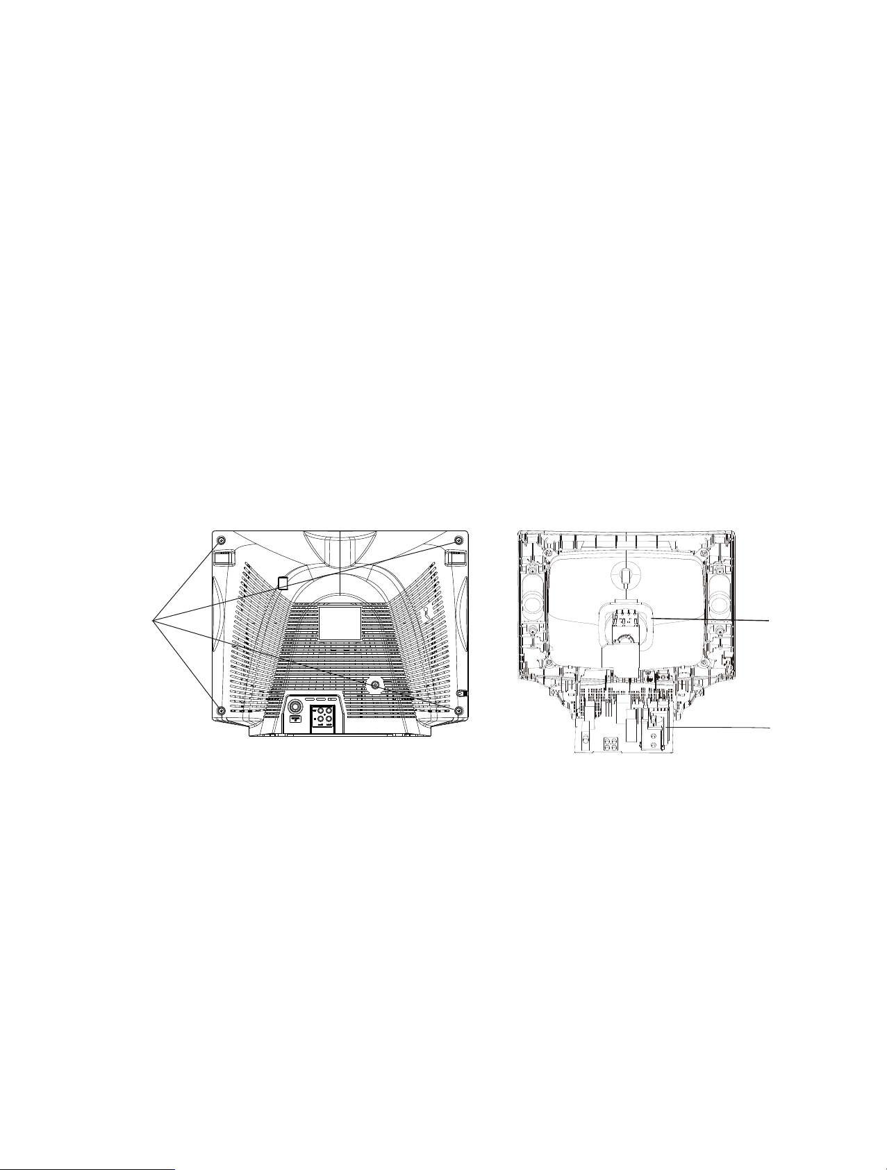
DISASSEMBLY INSTRUCTIONS
Important note
This set is disconnected from the power supply through the converter.
transformer. An isolating transformer is necessary for service
operations on the primary side of the converter transformer.
Back Cabinet Removal
Removal the screws residing on the back cabinet and carefully
separate the back cabinet from the front cabinet cabinet. (Fig. 2-1).
CPT Removal
1. Pull out the CPT board from the CPT neck.
2. Place the front cabinet on soft material not to mar the front surface
or damage control knobs.
3. Remove 4 screws securing the picture tube mounting brackets to
the front cabinet.
4. Carefully separate CPT from the front cabinet.
Chassis Assy Removal
Grasp both side of Frame and pull it backward smoothly.
PICTURE TUBE HANDLING CAUTION
Due to high vacuum and large surface area of picture tube, great care
must be exercised when handling picture tube. Always lift picture tube
by grasping it firmly around faceplate.
NEVER LIFT TUBE BY ITS NECK! The picture tube must not be
scratched or subjected to excessive pressure as fracture of glass may
result in an implosion of considerable violence which can cause
personal injury or property damage.
Remove
Screws
CPT
board
Main
PCB
8
Page 9

ADJUSTMENT
Safety Precautions
1. It is safe to adjust after using insulating transformer
between the power supply line and chassis input to
prevent the risk of electric shock and protect the
instrument.
2. Never disconnect leads while the TV receiver is on.
3. Don't short any portion of circuits while power is on.
4. The adjustment must be done by the correct appliances.
But this is changeable in view of productivity.
5. Unless otherwise noted, set the line voltage to
110~240Vac ± 10%, 50/60Hz.
6. The adjustment of TV should be performed after
warming up for 20 minutes.
SVC3
FMWS 2
MONO 1
DSG 1
AGN 0
AVL 1
BPB 0
AVLE 1
AMLOW 0
BPB2 1
FF1 0
MAXVOL 100
DCXO 1
BGDM 0
PLL.SEL 1
Test Equipment required
1 . Multi meter (volt meter)
2. Oscilloscope
3. 10:1 PROBE
OPT1
4. Color Analyzer
INCH 0
CDL Data Adjustment(LINE SVC-0)
1) Press the SVC button to get into the SVC-0 Mode.
2) Press the Channel UP/DOWN button to select CDLl2.
3) Press the Volume UP/DOWN button until the CDL data
is the same as the Table below.
14" SLIM
CDL Data 07
Remark SLIM
SYS 1
200PR 1
CH-AU 0
SND 0
S/AV 1
4) Press the OK button to memorize the data.
= OPTION Data Adjustment(OPTION-l,OPTION-2)
1) Press OK buttons on both TV set and Remote
Controller at the same time to get into SVC mode.
2) Press the Yellow button several times to find OPTION data.
3) Input the correspond OPTION data referring to Table
OPT2
VOL 1
H-DEV 1
MM 1
below with the numeric buttons.
4) Press the OK button to memorize the data.
EYE 0
DEG 0
Table 1. Function
IK 1
SVC1
AGC 27
WR 32
WG 32
WB 32
BLO-R 32
BLO-G 32
BLO-B 32
CDL 7
L-DLY 8
00.B 15
SVC2
V SLOP 27
VA 34
VS 33
HL 34
SL 26
EW WI 0
EW PA 0
EW UP 0
EW LO 0
EW TR 0
H PAR 0
H BOW 0
V-LIN 0
V SCROL 0
V ZOOM 0
WBR 0
WBF 0
V -SLY 0
DVD 0
OPT3
HOTEL 0
XD/TU 1
TURBO 1
X WAVE 0
TR/IC 1
OPT4
OSD LANG 1 0: ENG 1: HINDI
BLUE BACK 1 0: DISABLE 1: ENABLE
SVC4
WS 0
BKS 1
BSD 1
DSK 0
COR 0
PF 3
RPO 0
RPA 2
PWL 0
IFOFF 9
CHSE 1
ACL 0
BLOC 5
TEXT-V 40
TEXT-H 5
VGAURD 0
TER 1
GAM 1
0: W/O EW
1: W EW
0: 4 SYSTEM (BG/DK/I)
1: 3 SYSTEM (BG/DK/I)
0: OFF
1: ON
0: OFF
1: ON
0: MONO
0: AV-STEREO
0: 2AV
1: 1AV
0:LOW CARVE
1: HIGH CARVE
0: SOUND HIGH DEVIATION OFF
1: SOUND HIGH DEVIATION ON
0: W/O MUSIC MODE
1: W MUSIC MODE
0: W/O EYE
1: WITH EYE
0: W/O DEGAUSS
1: WITH DEGAUSS
0: IK OFF
1: IK ON
0: W/O COMP
1: WITH COMP
0:HOTEL MODE OFF
1: HOTEL MODE ON
0: TURBO PICTURE ON
1: XDP
0: W/O TURBO PICTURE
1: WITH TURBO PICTURE
0: W/O X WAVE
1: WITH X WAVE
0: IC BASE
1: TRANSISTOR BASE
9
Page 10

AGC Adjustment (SERVICE 1)
Test Point :AGC TP (C102)
Adjust :Remote Controller
1) Connect RF signal (70dBt0.2d8) and turn on the TV.
Standard adjustment Channel
-EU 05 Ch. (frf= 175.25MHz)
2) Press the OK buttons on TV set and Remote Controller
at the same time to get into SVC-0 mode.
3) In SVC-0 option, AGCTO is meant for AGC.
4) Press the Volume UP/DOWN button until the AGC
Voltage is the same as the Table below.
5) Press the OK button to memorize the data.
Tuner P/N 6700MF0018B
Marker LG Innotek(TBS TUNER)
AGC Voltage 2.4 ± 0.05V
FOCUS Adjustment
Test Point : Observing Display
Adjust : Focus Volume of FBT
1 )Tune the TV set to receive a PAL OSCH.
2) Adjust the Focus Volume of FBT for best focus.
Screen voltage Adjustment
Test Point : Rk ( Red cathode of CPT board)
Adjust : Screen volume of FBT
1)Connect the probe of oscilloscope to the RK (Red
Cathode) of CPT Board.
2)Set the oscilloscope to 50V/div and 20Us/div and after
putting GND line upon the lowest grid line of the scope
by pressing GND button, enter into DC mode.
3) Tune the TV set to receive a PAL-BG O5GH.
4) Adjust Screen Volume of FBT so that the waveform is
the same as below figure (DC 100V).
Black level
100Vp-p
White level
GND for dc
140Vp_p
leve
Horizornal
FIyBack Time
W h i t e
White Balance Adjustment.(LINE SVC-0)
NOTE : This adjustment should be performed after screen
voltage adjustment.
1)Tune the TV set to receive an 100% white pattern.
2)Press OK buttons on TV set and remote controller at
the same time to get into SVC mode.
3) Use the CH CH Key to chose adjustment item.
4) Use the VOL VOL Key to change item data.
5) Adjustment.
a)Make the picture luminance 4.5 changing the
" CONTRAST" and "BRIGHTNESS".
b)Adjust X data of low light with BLO-R and Y data with
BLO-B.
c)Adjust X dada of High light RG and Y data with BG.
d) Repeat steps b~c until both low & high light hare same
readings as shown below.
L X- Data Y-Data
Low Light 255 260
High Light 260 265
Status Initial Data Remark
RG 32
GG 32
BG 32
BLO-R 32
BLO-G 32
BLO-B 32
6) Press the OK button to memorize the data.
10
Page 11

Deflection Data Adjustment (Line SVC-1 )
NOTE: To enter SVC mode, press "OK" buttons on both TV set
and the Remote control at the same time.
1. Preparation for Deflection Adjustment
1 ) At SVC mode, press the "IN- START" key.
And then, deflection data adjustment OSD (SVC1 mode)
will be displayed.
2) Tune the TV set to receive a PAL 05 CH and set the ARC
mode is standard.
2. Deflection Initial Setup Data
Status 14" SLIM
VSLOP 27
VA 34
VS 33
HS 34
SC 25
3. Deflection Adjustment Procedure
VSLOP (Vertical Slope)
Adjust so that the boundary line between upper and lower half is in
accord with geometric horizontal center of the CPT.
VA (Vertical Amplitude)
Adjust so that the circle of a digital circle pattern may be located within
the effective screen of the CPT.
SC (Vertical "S" Correction)
Adjust so that all distance between each horizontal lines are to be the
same.
VS (Vertical Shift)
Adjust so that the horizontal center line of a digital circle pattern is in
accord with geometric horizontal center of the CPT.
HS (Horizontal Shift)
Adjust so that the vertical center line of a digital circle pattern is i n
accord with geometric vertical center of the CPT.
Press the OK button to memorize the data.
11
Page 12

PURITY & CONVERGENCE ADJUSTMENT
Caution:
Convergence and Purity have been factory aligned. Do not attempt to
tamper with these alignments.
However, the effects of adjacent receiver components, or
replacement of picture tube or deffection yoke may require the need
to readjust purity any convergence.
DEFLECTION YPKE
PURITY%CONVERGENCE
MAGNET ASSEMBLY
6-POLE
X-AXISYOKE MAGNET
POSITIONING
(L/R PURITY)
RUBBER
WEDGES
PURITY MAGNET
4-POLE
GLASS CLOTH TAPE
5. Reconnect the internal degaussing coil.
6. Position the beam bender locking rings at the 9 o'clock position
and the other three pairs of tabs (2,4 and 6 pole magnets) at the
12 o'clock position.
6-POLE
MAGNETS
4-POLE
CONVERGENCE MAGNET ASSEMBLY
PURITY MAGNET(2-POLE)
Purity Adjustment
This procedure DOES NOT apply to bonded yoke and picture tube
assemblies.
The instrument should be at room temperature (60 degress F or
above) for six (6) hours and be operating at low beam current (dark
background) for approximately 20 to 30 minutes before performing
purity adjustments.
CAUTION: Do not remove any trim magnets that may be attached
to the bell of the picture tube.
1. Remove the AC power and disconnect the internal degaussing
coil.
2. Remove the yoke from the neck of the picture tube.
3. If the yoke has the tape version beam bender, remove it and
replace it with a adjustable type beam bender (follow the
instructions provided with the new beam bender)
4. Replace the yoke on the picture tube neck, temporarily remove
the three (3) rubber wedges from the bell of the picture tube and
then slide the yoke completely forward.
7. Perform the following steps, in the order given, to prepare the
receiver for the purity adjustment procedure.
a. Face the receiver in the "magnetic north" direction.
b. Externally dsgauss the receiver screen with the television
power turned off.
c. Turn the television on for approximately 10 seconds to perform
internal degaussing and then turn the TV off.
d. Unplug the internal degaussing coil. This allows the thermistor
to cool down while you are performing the purity adjustment.
DO NOT MOVE THE RECEIVER FROM ITS "MAGNETIC
NORTH" POSITION.
e. Turn the receiver on and obtain a red raster by increasing the
red bias control (CW) and decreasing the bias controls for the
remaining two colors (CCW).
f. Attach two round magnets on the picture tube screen at 3
o'clock and 9 o'clock positions, approximately one (1 ) inch from
the edge of the mask (use double-sided tape).
12
Page 13

1.ADJUST YOKE Z-AXIS FIRST
TO GET EQUAL BLUE
COLOR CIRCLES
MAGNETS
1.ADJUST BEAM BENDER 2 POLE
MAGNET TO GET FOUR EQUAL
COLOR CIRCLES
RED
8. Referring to above, perform the following two steps:
a. Adjust the yoke Z-axis to obtain equal blue circles.
b. Adjust the appropriate beam bender tabs to obtain correct purity
(four equal circles).
9. After correct purity is set, tighten the yoke clamp screw and
remove the two screen magnets.
10. Remove the AC power and rotate the receiver 180 degrees
(facing "magnetic south").
11. Reconnect the internal degaussing coil.
12. Turn the receiver on for 10 seconds (make sure the receiver
came on) to perform internal degaussing, and then turn the
receiver off.
13. Unplug the internal degaussing coil.
14. Turn on the receiver and check the purity by holding one (1)
round magnet at the 3 o'clock and a second round magnet at 9
o'clock position. If purity is not satisfactory, repeat steps 8
through 14.
15. Turn off the receiver and reconnect the internal degaussing coil.&
Convergence Adjustment
Caution: This procedure DOES NOT apply to bonded yoke and
picture tube assemblies.
Do not use screen magnets during this adjustment
procedure. Use of screen magnets will cause an incorrect
display.
1. Remove AC power and disconnect the internal degaussing coil.
2. Apply AC Power and set the brightness to the Picture Reset
condition. Set the Color control to minimum.
3. Make a horizontal line.
4. Adjust the Red, Green and Blue Bias controls to get a dim white
line.
RED
6. Reconnect the internal degaussing coil and apply AC power.
7. Turn he receiver on for 10 seconds to perform internal
degaussing and then turn the receiver off again.
8. Unplug the internal degaussing-coil.
9. Turn on the receiver, connect a signal generator to the VHF
antenna terminal and apply a crosshatch signal.
Caution: During the convergence adjustment procedure, be very
careful not to disturb the purity adjustment tabs are
accidentally move, purity should be confirmed before
proceeding with the convergence adjustments.
Note: Make sure the focus is set correctly on this instrument
before proceeding with the following adjustment.
10. Converge the red and blue vertical lines to the green vertical line
at the center of the screen by performing the following steps
(below TABLE).
a. Carefully rotate both tabs of the 4-pole ring magnet
simultaneously in opposite directions from the 12 o'clock
position to converge the red and blue vertical lines.
b. Carefully rotate both tabs of the 6-pole ring magnet
simultaneously in opposite directions form the 12 o'clock
position to converge the red and blue (now purple)
vertical lines with the green vertical line.
11. Converge the red and blue horizontal with the green line at the
center of the screen by performing the following steps. (below
TABLE)
a. Carefully rotate both tabs of the 4-pole ring magnet
simultaneously in the same direction (keep the spacing
between the two tabs the same) to converge the red and
blue horizontal lines.
b. Carefully rotate both tabs of the 6-pole ring magnet
simultaneously in same direction (keep the spacing
between the two tabs the same) to converge the red and
blue (nowpurple) horizontal lines with the green
horizontal line.
c. Secure the tabs previsouly adjusted by locking them in
place with the locking tabs on the beam bender.
5. Restore the screen by removing the horizontal line.
13
Page 14

RING
PAIRS
ROTATION DIRECTION
OF BOTH TABS
MOVEMENT OF RED
AND BLUE BEAMS
4
POLE
6
POLE
UP/DOWN ROCKING OF THE YOKE
CAUSES OPPOSITE ROTATION OF RED
AND BLUE RASTERS
GREEN
OPPOSITE
SAME
OPPOSITE
SAME
B
B
OR
R
R
B
OR
R
R
B
B B
OR
R R
R
B
LEFT/RIGHT ROCKING OF THE YOKE
CAUSES OPPOSITE SIZE CHANGE OF THE
RED AND BLUE RASTERS
OR
R
B
ADJUSTMENT
VIEWING
AREA
GREEN
BLUE
RED
ER D
UE
L
B
RED
BLUE
GREEN
L
B UE
R
ED
GREEN
12. While watching the 6 o'clock positions on the screen, rock the
front of the yoke in a vertical (up/down) direction to converge the
red and blue vertical lines. (Fig upper left)
13. Temporarily place a rubber wedge at the 12 o'clock position to
hold the vertical position or the yoke.
14. Check the 3 o'clock and 9 o'clock areas to confirm that the red
and blue horizontal lines are converged.
If the lines are not converged, slightly offset the vertical tilt of the
yoke (move the rubber wedge if necessary) to equally balance
the convergence error of the horizontal tines at 3 o'clock and 9
o'clock and the vertical lines at 6 o'clock and 12 o'clock.
15. Place a 1.5 inch piece of glass tape over the rubber foot at the
rear of the 12 o'clock wedge.
16. While watching the 6 o'clock and 12 o'clock areas of the screen,
rock the front of the yoke in the horizontal (left to right) motion to
converge the red and blue horizontal lines. (Fig. upper right)
ADJUSTMENT
VIEWING
AREA
RED
BLUE
GREEN
R
E
D
TV
SCREEN
17. Temporarily place a rubber wedge at the 5 o'clock and 7 o'clock
positions to hold the horizontal position of the yoke.
18. Check the 3 o'clock and 9 o' clock areas to confirm that the red
and blue vertical lines are converged. If the lines are not
converged, slightly offset the horizontal tilt of the yoke (move the
temporary rubber wedges if necessary) to equally balance the
convergence error of the horizontal lines at 6 o'clock and 12
o'clock and the vertical lines at 3 o'clock and 9 o'clock.
19. Using a round magnet confirm purity at the center, right and left
sides and corners. See Purity Adjustment Procedure.
20. Reconfirm convergence and apply a 1.5 inch piece of glass tape
over the rubber toot at the rear of the 5 o'clock and the 7 o'clock
wedges.
14
Page 15

L401
Option Part
IIC Bus Line
SMPS
TRANS
10.5V
14
Zener
Regulator
ST-5V
P02A
P02A
(Pre amp/LED)
(Pre amp/LED)
IC804
IC04
(ST-3.3V REG)
9V
ST-3.3V
EER3940
For SW
(9V
REG)
IC803
(5V REG)
5V
V_DY
B+
2
4
1
(Vertical Amp)
IC301 TDA4863AJ
7
6
14
15
VA
VB
37
PWR
IR
39
H_DY
1
Q401
Collector
2SC6090
FBT
14V
3
35
34
SCL/SDA
58
A OUT
200V
-14V
4
7
5
ABL
28V
8
IC02
EEPROM
HD
9
AT24C16
CP79C BLOCK DIAGRAM
CP79C BLOCK DIAGRAM
1
AV_Out (V,L)
27
KEY
A IN V OUT
IC501 UOC Top
IC501 UOC Top
62 63
V IN
Rear_AV AV IN (V, L)
(Front Local Key)
47~44
Ik,R/G/B OUT
28
EYE
SPK OUT
59
P902A
(To CPT B/D)
IC602 TDA2006
IC602 TDA2006
(Sound Amp MONO)
(Sound Amp MONO)
IF IN
12 13
VIF
SAW
Z111
SAW
Z111
IF
IF
5V
5V
33V
33V
SDA
SCL
SDA
SCL
(((
SPK OUT
(
15
Page 16

R,G,B SECTION
R,G,B SECTION
ABL CIRCUIT
IC 501
brightness
reduction
(2.5V)
contrast
reduction
(3.5V)
BEAM CURRENT
48
J517
C548
10uF/50V
D501
4148
R415
6.8K
R402
1.2K
RS/1/2W
A
R416
91K
RS/1/2W
B+
R406
1K
C402
0.022UF
200V(M)
FBT
T402
9
ABL
To protect the picture tube and FBT,the average beam current an d peak beam current may not to high.
The beam current limit information and High Voltage(H.V) tracking information are derived from
the H.V voltage winding of T401 (point A).
1. The contrast and brightness reduction of RGB is proportional to the voltage on the pin 48 of IC501.
2. As the beam current(slow),and H.V (fast) are changes, the voltage of point A is changed.
3. By the increase of beam current ,the point A voltage is decreased and this information is fed to pin 48 of IC501.
- Contrast reduction begins when V49 is below than 3.1V.
- By the more increasing of the beam current , the V48 decreased and eventually when this voltage is less than
1.8V the brightness reduction is started.
Deflection SECTION
HORIZONTAL DRIVE CIRCUIT
IC501
56
H-OUT
R555
R556
5V
J546
H.Vcc
R404C403
Q401
C2331Y
ZD418
C402
Q402
R413
C404
T403
HDT
2SC6093
Q402
R401
i1(t1.t2)
i2(t2.t3)
i4(t4.t5)
FB401
i3(t3.t4)
C414
CT
H-DY
C412
CS
FBT
i5
1
Winding
2
B+
110V
Primary
1. The H drive output is open collector and active low,
I.e. the H-out TR should conduct during the low period
of output.
2. Under normal operation condition the duty cycle of the
output pulse is 50%.
3. To ensure a smooth start/stop behavior of the horizontal
deflection and protect the H-out TR, there are 3 different
condition of H-drive output.
During switch-on.
The horizontal output starts with the double frequency
(31KHz) and with duty of 75%(off),25%(on).
After about 50mSec of switch-on.
The frequency is changed to normal value(15.625KHz)
and duty cycle to 50%.
During switching-off.
Also the frequency is switched to the double value and
R.G.B drive is set to Max. and after 100mSec R.G.B
is set to Min. and 50mSec later the H drive is switch-off.
4. The H drive pulse from the MICOM (IC 501)
horizontal drive circuit,to get sufficient base drive current
for the high voltage switching TR(Q402).
is amplified by the
VB of Q402
Collector
Current
of Q402
The Voltage
at H-DY
The current
of resonant
Capacitor
(C414)
DAMP
current
Deflection
current of
H-DY
tr : retrace period
16
t1 t2t3t4 t5 t6
i2
i1
i3
i4
ts : scannig period
t1 : Q402 is switched on.
t
t1.t2
: Collector current of Q402 increases linearly.
i1 flows from C412 Which have been charged
t
at the end of first half of scan.
i5 also flows, energy stored in the primary
winding(.) ) of FBT.
t2 : Q402 is switched off abruptly.
t2.t3
: Reverse EMF of H-DY maintains i1 direction
and charges C414.
Reverse EMF of the FBT primary occurs to
maintain is direction.
t3 : Q402 is still off.
t3.t4
: C414 discharges through H-DY.
t4.t5
: H-DY attempts to maintain i3 direction.
Damping diode becomes forward biased
and C412 is charged.
Page 17

AUDIO AMP. SECTION
TDA2006
through R626, R608 [Input level adjust] and C622, [AC coupling].
- Audio signal from the PIN 58 of IC501 are applied to PIN1
CIRCUIT ANALYSIS
AUDIO IN
FEEDBACK
IN
ROLE DESCRIPTION
MINIMUM EXTERNAL COMPONENTS
INTERNALLY FIXED GAIN
THERMAL OVERLOAD PROTECTION
TDA2006
TDA2006
8W MONO AMPLIFIER
WIDE SUPPLY VOLTAGE RANGE (12.30V)
•••••
FEATURES :
SHORT CIRCUIT PROTECTION
Pin descriptions of TDA7297
Pin descriptions of TDA7297
Pin NO
FB
1
2
AUDIO OUT
SOUND GND
SGND
3
SOUND SVCC
OUT
SVCC
4
5
• Q621 is for muting audio in.
17
Page 18

EXPLODED VIEW
P801
913
112
170
150
500
400
410
300
120
18
Page 19

LOCATION
150
170
300
400
500
913
P801
EAK51682104
EAB42432101
61409C2010E
EAD52408203
ABJ72911401
ACQ73029201
EBT6071201
FAB30021401
EAD53594701
CPT ASSEMBLY, A34KVL420X 01 K 14 INCH ULTRA SLIM LPDI.
SPEAKER, MID-RANGE
Coil, Degaussing
CPT EARTH
Cover Assembly, 14SB2RB-AJ
BACK COVER ASSEMBLY,
Chassis Assembly
Screw Assembly
POWER CORD,ISI 2000 (GROOMET 325)MM . BLACK
19
Page 20

PART NO PART NOLOCATION
Resistors
C117 0RN3902F409
FR401 0RF0470K607
FR403 0RF0121H609
FR404 0RP0050H709
FR405 0RP0050H709
FR406 0RP0050H709
FR825 0RP0020J809
J154 0RD4300F609
J241 0RD7501F609
J246 0RD7501F609
J501 0RD1000F609
J609 0RD5601F609
L101 0RD0392F609
L207 0RD2200F609
L208 0RD0752F609
R1 0RD1301F609
R100 0RD0562F609
R101 0RD1000F609
R102 0RD3601F609
R103 0RD1201F609
R104 0RD0272F609
R105 0RD6800F609
R110 0RS2702H609
R120 0RD1003F609
R134 0RD1002F609
R16 0RD1001F609
R17 0RD1501F609
R178 0RD4701F609
R179 0RD1803F609
R18 0RD2001F609
R19 0RD4300F609
R2 0RD1001F609
R20 0RD3000F609
R205 0RD0752F609
R21 0RD2401F609
R303 0RN0471H609
R304 0RN0471H609
R305 0RD2400A609
R308 0RD6202F609
R309 0RD6202F609
R310 0RD0561A609
R311 0RD5601F609
R312 0RD5601F609
R313 0RD4702F609
R314 0RD4702F609
R401 0RD0332A609
R402 0RD1201F609
R403 0RD3300A609
R405 0RS8201K607
R406 0RS1001H609
LOCATION
R412 0RD7501A609
R413 0RD5600A609
R415 0RD6801F609
R416 0RS9102H609
R425 0RS1800K619
R441 0RD1002F609
R501 0RD4700F609
R502 0RD2200F609
R504 0RD3900F609
R507 0RD3902F609
R508 0RD3302F609
R511 0RD2200F609
R512 0RD2200F609
R513 0RD2200F609
R514 0RD1001F609
R520 0RD1202F609
R521 0RD8203F609
R522 0RD2200F609
R523 0RD1000F609
R524 0RD4701F609
R525 0RD2200F609
R541 0RD4701F609
R549 0RD1202F609
R555 0RD1501F609
R556 0RD1000F609
R58 0RD4701F609
R621 0RD1503F609
R622 0RD6801F609
R623 0RD1003F609
R624 0RD1003F609
R625 0RD1003F609
R626 0RD5601F609
R627 0RD3902F609
R628 0RD0331H609
R67 0RD3301F609
R68 0RD1000F609
R69 0RD3301F609
R70 0RD1000F609
R802 0RKZVTA001K
R803 0RD4701F609
R804 0RS3902K607
R805 0RS3902K607
R807 0RD2200A609
R808 0RD1501F609
R809 0RD1001F609
R810 0RD0332F609
R811 0RS0821K607
R812 0RD1003F609
R814 0RKZVTA001C
R815 0RN9102G409
R816 0RN9102G409
20
Page 21

PART NO PART NOLOCATION
LOCATION
Resistors
R82 0RD4701F609
R832 0RD4701F609
R835 0RD3001F609
R840 0RD0472F609
R841 0RD1001F609
R842 0RN2002F409
R843 0RD3902F609
R844 0RN4701F409
R845 0RD1001F609
R883 0RS1000K607
R901 0RD0472F609
R902 0RD1002F609
R904 0RD1002F609
R905 0RD1002F609
R906 0RD0472F609
R907 0RD0472F609
R908 0RD3300F609
R909 0RD3300F609
R910 0RD0472F609
R912 0RD0472F609
R915 0RD2204A609
R916 0RD3300F609
R917 0RS1802K607
R918 0RD2200F609
R919 0RS1802K607
R920 0RD3300F609
R921 0RD1501A609
R922 0RD2200F609
R923 0RS1802K607
R924 0RD2200F609
R925 0RD3300F609
R926 0RD3300F609
R927 0RD0472F609
R928 0RD1501A609
R929 0RD1501A609
Capacitors
C102 0CN1040K949
C103 0CE106DK618
C105 0CN1030F679
C107 0CN1030F679
C108 0CE226DF618
C110 0CE106DF618
C111 0CE476DF618
C112 0CN1020K519
C113 0CN1030F679
C115 0CN1030F679
C121 0CN1030F679
C207 0CN1030F679
C28 0CE107DD618
C303 0CK4710W515
C307 0CE107DJ618
C310 0CQ1041N409
C313 0CN2220F569
C314 0CQ2241N501
C315 0CN2220F569
C32 0CE476DD618
C40 0CE476DD618
C401 0CE475DR618
C402 181-009R
C403 0CE106DF618
C404 0CQ1521N509
C408 0CE225DP618
C413 0CK1010W515
C414 181-015G
C415 0CK4710W515
C416 181-009R
C417 181-091W
C419 0CE227CH638
C420 0CE227CH638
C421 0CK4710W515
C503 0CE476DF618
C504 0CQ1041N409
C506 0CE106DF618
C508 0CN1020K519
C511 181-301C
C516 0CN1040K949
C517 0CE107DF618
C518 0CQ2242K439
C519 0CE105DK618
C520 0CQ6821N509
C521 0CE107DD618
C522 181-007C
C523 0CE106DF618
C524 0CN1030F679
C525 0CN1030F679
C528 0CN1030F679
C537 0CE106DF618
C547 0CN1010K519
C548 0CE106DK618
C552 181-007C
C554 0CN1030F679
C555 0CE476DF618
C561 0CE105DK618
C562 181-007C
C563 0CQ6831N509
C564 0CE227DD618
C601 0CE107DD618
C602 0CQ1041N409
C613 0CE107DJ618
21
Page 22

PART NO
LOCATION
PART NOLOCATION
Capacitors
C621 0CN1010K519
C622 0CE225DK618
C623 0CE336BK618
C624 0CE107DJ618
C625 0CQ1041N509
C626 0CE226DK618
C802 0CQZVBK002C
C804 0CK10202515
C805 0CK10202515
C807 181-033R
C809 0CE105DK618
C810 0CE336DK618
C813 181-033S
C815 0CK8210K515
C816 0CE107CP618
C817 181-007C
C818 0CQ2231N509
C819 0CK1520K515
C820 0CE476DD618
C821 0CK1520W515
C826 0CE228BF618
C828 0CE476DD618
C831 0CE227DJ618
C833 0CE107DD618
C843 181-120K
C847 0CE105BR618
C850 0CE477DF618
C853 0CE107DH618
C902 0CE475DR618
C903 0CN3310K519
C904 0CN5610K519
C905 0CN5610K519
C906 0CK12202510
Diodes
D177 0DD414809ED
D301 0DD060009AC
D302 0DD400509AA
D402 0DD060009AC
D405 0DD060009AC
D501 0DD414809ED
D801 0DRDC00014Q
D802 0DRDC00014J
D803 0DRDC00014J
D813 0DRDC00014G
D826 0DRDC00014F
D834 0DRDC00014F
D901 0DRDC00014R
D902 0DD414809ED
D903 0DD414809ED
D904 0DD414809ED
DB801 0DRTW00131A
ZD05 0DZ910009BD
ZD06 0DZ910009BD
ZD07 0DZ910009BD
ZD08 0DZ910009BD
ZD102 0DZ330009DF
ZD401 0DZ510009BF
ZD418 0DD414809ED
ZD503 0DZ820009AH
ZD511 0DZ910009BD
ZD512 0DZ910009BD
ZD513 0DZ910009BD
ZD514 0DZ820009AH
ZD802 0DZ510009BF
ZD851 0DZ910009BD
22
Page 23

PART NO
LOCATION
Transistors IC
PART NOLOCATION
Q10 0TR319809AA
Q101 0TR319709AB
Q401 0TR233109AA
Q502 0TR198009BA
Q621 0TR534309AA
Q801 0TR534309AA
Q813 0TR102009AB
Q901 0TR233009CA
Q902 0TR421009CC
Q903 0TR233009CA
Q904 0TR233009CA
Q905 0TR421009CC
Q906 0TR233009CA
Q907 0TR233009CA
Q908 0TR233009CA
Q909 0TR421009CC
IC02 0IAL241600B
IC301 0IPMGPH002A
IC501 EAN57863702
IC601 0ISG200600A
IC801 0IPMGSK016A
IC802 0IPRPKD003A
IC803 0IKE780500Q
IC805 0IMCRAU004A
IC806 0IMCRKE002B
Q840 0IMCRFA007A
23
Page 24

Page 25

LG Electronics LG Electronics
 Loading...