

Page 1

LCD TV
SERVICE MANUAL
CAUTION
BEFORE SERVICING THE CHASSIS,
READ THE SAFETY PRECAUTIONS IN THIS MANUAL.
CHASSIS : LA75E
MODEL : 19LC2D 19LC2D-UB
website:http://biz.LGservice.com
Page 2

- 2 -
Copyright © 2007 LG Electronics. Inc. All right reserved.
Only for training and service purposes
LGE Internal Use Only
CONTENTS
CONTENTS .............................................................................................. 2
SAFETY PRECAUTIONS ..........................................................................3
SPECIFICATION ........................................................................................6
ADJUSTMENT INSTRUCTION .................................................................8
TROUBLE SHOOTING ............................................................................12
BLOCK DIAGRAM...................................................................................16
EXPLODED VIEW .................................................................................. 18
SVC. SHEET ...............................................................................................
Page 3
Copyright © 2007 LG Electronics. Inc. All right reserved.
Only for training and service purposes
LGE Internal Use Only
- 3 -
SAFETY PRECAUTIONS
Many electrical and mechanical parts in this chassis have special safety-related characteristics. These parts are identified by in the
Schematic Diagram and Replacement Parts List.
It is essential that these special safety parts should be replaced with the same components as recommended in this manual to prevent
Shock, Fire, or other Hazards.
Do not modify the original design without permission of manufacturer.
General Guidance
An isolation Transformer should always be used during the
servicing of a receiver whose chassis is not isolated from the AC
power line. Use a transformer of adequate power rating as this
protects the technician from accidents resulting in personal injury
from electrical shocks.
It will also protect the receiver and it's components from being
damaged by accidental shorts of the circuitry that may be
inadvertently introduced during the service operation.
If any fuse (or Fusible Resistor) in this TV receiver is blown,
replace it with the specified.
When replacing a high wattage resistor (Oxide Metal Film Resistor,
over 1W), keep the resistor 10mm away from PCB.
Keep wires away from high voltage or high temperature parts.
Before returning the receiver to the customer,
always perform an AC leakage current check on the exposed
metallic parts of the cabinet, such as antennas, terminals, etc., to
be sure the set is safe to operate without damage of electrical
shock.
Leakage Current Cold Check(Antenna Cold Check)
With the instrument AC plug removed from AC source, connect an
electrical jumper across the two AC plug prongs. Place the AC
switch in the on position, connect one lead of ohm-meter to the AC
plug prongs tied together and touch other ohm-meter lead in turn to
each exposed metallic parts such as antenna terminals, phone
jacks, etc.
If the exposed metallic part has a return path to the chassis, the
measured resistance should be between 1MΩ and 5.2MΩ.
When the exposed metal has no return path to the chassis the
reading must be infinite.
An other abnormality exists that must be corrected before the
receiver is returned to the customer.
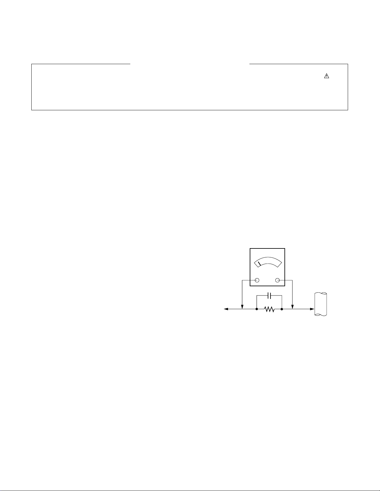
Leakage Current Hot Check (See below Figure)
Plug the AC cord directly into the AC outlet.
Do not use a line Isolation Transformer during this check.
Connect 1.5K/10watt resistor in parallel with a 0.15uF capacitor
between a known good earth ground (Water Pipe, Conduit, etc.)
and the exposed metallic parts.
Measure the AC voltage across the resistor using AC voltmeter
with 1000 ohms/volt or more sensitivity.
Reverse plug the AC cord into the AC outlet and repeat AC voltage
measurements for each exposed metallic part. Any voltage
measured must not exceed 0.75 volt RMS which is corresponds to
0.5mA.
In case any measurement is out of the limits specified, there is
possibility of shock hazard and the set must be checked and
repaired before it is returned to the customer.
Leakage Current Hot Check circuit
1.5 Kohm/10W
To Instrument's
exposed
METALLIC PARTS
Good Earth Ground
such as WATER PIPE,
CONDUIT etc.
AC Volt-meter
IMPORTANT SAFETY NOTICE
0.15uF
Page 4

Copyright © 2007 LG Electronics. Inc. All right reserved.
Only for training and service purposes
LGE Internal Use Only
- 4 -
CAUTION: Before servicing receivers covered by this service
manual and its supplements and addenda, read and follow the
SAFETY PRECAUTIONS on page 3 of this publication.
NOTE: If unforeseen circumstances create conflict between the
following servicing precautions and any of the safety precautions on
page 3 of this publication, always follow the safety precautions.
Remember: Safety First.
General Servicing Precautions
1. Always unplug the receiver AC power cord from the AC power
source before;
a. Removing or reinstalling any component, circuit board
module or any other receiver assembly.
b. Disconnecting or reconnecting any receiver electrical plug or
other electrical connection.
c. Connecting a test substitute in parallel with an electrolytic
capacitor in the receiver.
CAUTION: A wrong part substitution or incorrect polarity
installation of electrolytic capacitors may result in an
explosion hazard.
2. Test high voltage only by measuring it with an appropriate high
voltage meter or other voltage measuring device (DVM,
FETVOM, etc) equipped with a suitable high voltage probe.
Do not test high voltage by "drawing an arc".
3. Do not spray chemicals on or near this receiver or any of its
assemblies.
4. Unless specified otherwise in this service manual, clean
electrical contacts only by applying the following mixture to the
contacts with a pipe cleaner, cotton-tipped stick or comparable
non-abrasive applicator; 10% (by volume) Acetone and 90% (by
volume) isopropyl alcohol (90%-99% strength)
CAUTION: This is a flammable mixture.
Unless specified otherwise in this service manual, lubrication of
contacts in not required.
5. Do not defeat any plug/socket B+ voltage interlocks with which
receivers covered by this service manual might be equipped.
6. Do not apply AC power to this instrument and/or any of its
electrical assemblies unless all solid-state device heat sinks are
correctly installed.
7. Always connect the test receiver ground lead to the receiver
chassis ground before connecting the test receiver positive
lead.
Always remove the test receiver ground lead last.
8. Use with this receiver only the test fixtures specified in this
service manual.
CAUTION: Do not connect the test fixture ground strap to any
heat sink in this receiver.
Electrostatically Sensitive (ES) Devices
Some semiconductor (solid-state) devices can be damaged easily
by static electricity. Such components commonly are called
Electrostatically Sensitive (ES) Devices. Examples of typical ES
devices are integrated circuits and some field-effect transistors and
semiconductor "chip" components. The following techniques
should be used to help reduce the incidence of component
damage caused by static by static electricity.
1. Immediately before handling any semiconductor component or
semiconductor-equipped assembly, drain off any electrostatic
charge on your body by touching a known earth ground.
Alternatively, obtain and wear a commercially available
discharging wrist strap device, which should be removed to
prevent potential shock reasons prior to applying power to the
unit under test.
2. After removing an electrical assembly equipped with ES
devices, place the assembly on a conductive surface such as
aluminum foil, to prevent electrostatic charge buildup or
exposure of the assembly.
3. Use only a grounded-tip soldering iron to solder or unsolder ES
devices.
4. Use only an anti-static type solder removal device. Some solder
removal devices not classified as "anti-static" can generate
electrical charges sufficient to damage ES devices.
5. Do not use freon-propelled chemicals. These can generate
electrical charges sufficient to damage ES devices.
6. Do not remove a replacement ES device from its protective
package until immediately before you are ready to install it.
(Most replacement ES devices are packaged with leads
electrically shorted together by conductive foam, aluminum foil
or comparable conductive material).
7. Immediately before removing the protective material from the
leads of a replacement ES device, touch the protective material
to the chassis or circuit assembly into which the device will be
installed.
CAUTION: Be sure no power is applied to the chassis or circuit,
and observe all other safety precautions.
8. Minimize bodily motions when handling unpackaged
replacement ES devices. (Otherwise harmless motion such as
the brushing together of your clothes fabric or the lifting of your
foot from a carpeted floor can generate static electricity
sufficient to damage an ES device.)
General Soldering Guidelines
1. Use a grounded-tip, low-wattage soldering iron and appropriate
tip size and shape that will maintain tip temperature within the
range or 500°F to 600°F.
2. Use an appropriate gauge of RMA resin-core solder composed
of 60 parts tin/40 parts lead.
3. Keep the soldering iron tip clean and well tinned.
4. Thoroughly clean the surfaces to be soldered. Use a mall wirebristle (0.5 inch, or 1.25cm) brush with a metal handle.
Do not use freon-propelled spray-on cleaners.
5. Use the following unsoldering technique
a. Allow the soldering iron tip to reach normal temperature.
(500°F to 600°F)
b. Heat the component lead until the solder melts.
c. Quickly draw the melted solder with an anti-static, suction-
type solder removal device or with solder braid.
CAUTION: Work quickly to avoid overheating the circuit
board printed foil.
6. Use the following soldering technique.
a. Allow the soldering iron tip to reach a normal temperature
(500°F to 600°F)
b. First, hold the soldering iron tip and solder the strand against
the component lead until the solder melts.
c. Quickly move the soldering iron tip to the junction of the
component lead and the printed circuit foil, and hold it there
only until the solder flows onto and around both the
component lead and the foil.
CAUTION: Work quickly to avoid overheating the circuit
board printed foil.
d. Closely inspect the solder area and remove any excess or
splashed solder with a small wire-bristle brush.
SERVICING PRECAUTIONS
Page 5

Copyright © 2007 LG Electronics. Inc. All right reserved.
Only for training and service purposes
LGE Internal Use Only
- 5 -
IC Remove/Replacement
Some chassis circuit boards have slotted holes (oblong) through
which the IC leads are inserted and then bent flat against the
circuit foil. When holes are the slotted type, the following technique
should be used to remove and replace the IC. When working with
boards using the familiar round hole, use the standard technique
as outlined in paragraphs 5 and 6 above.
Removal
1. Desolder and straighten each IC lead in one operation by gently
prying up on the lead with the soldering iron tip as the solder
melts.
2. Draw away the melted solder with an anti-static suction-type
solder removal device (or with solder braid) before removing the
IC.
Replacement
1. Carefully insert the replacement IC in the circuit board.
2. Carefully bend each IC lead against the circuit foil pad and
solder it.
3. Clean the soldered areas with a small wire-bristle brush.
(It is not necessary to reapply acrylic coating to the areas).
"Small-Signal" Discrete Transistor
Removal/Replacement
1. Remove the defective transistor by clipping its leads as close as
possible to the component body.
2. Bend into a "U" shape the end of each of three leads remaining
on the circuit board.
3. Bend into a "U" shape the replacement transistor leads.
4. Connect the replacement transistor leads to the corresponding
leads extending from the circuit board and crimp the "U" with
long nose pliers to insure metal to metal contact then solder
each connection.
Power Output, Transistor Device
Removal/Replacement
1. Heat and remove all solder from around the transistor leads.
2. Remove the heat sink mounting screw (if so equipped).
3. Carefully remove the transistor from the heat sink of the circuit
board.
4. Insert new transistor in the circuit board.
5. Solder each transistor lead, and clip off excess lead.
6. Replace heat sink.
Diode Removal/Replacement
1. Remove defective diode by clipping its leads as close as
possible to diode body.
2. Bend the two remaining leads perpendicular y to the circuit
board.
3. Observing diode polarity, wrap each lead of the new diode
around the corresponding lead on the circuit board.
4. Securely crimp each connection and solder it.
5. Inspect (on the circuit board copper side) the solder joints of
the two "original" leads. If they are not shiny, reheat them and if
necessary, apply additional solder.
Fuse and Conventional Resistor
Removal/Replacement
1. Clip each fuse or resistor lead at top of the circuit board hollow
stake.
2. Securely crimp the leads of replacement component around
notch at stake top.
3. Solder the connections.
CAUTION: Maintain original spacing between the replaced
component and adjacent components and the circuit board to
prevent excessive component temperatures.
Circuit Board Foil Repair
Excessive heat applied to the copper foil of any printed circuit
board will weaken the adhesive that bonds the foil to the circuit
board causing the foil to separate from or "lift-off" the board. The
following guidelines and procedures should be followed whenever
this condition is encountered.
At IC Connections
To repair a defective copper pattern at IC connections use the
following procedure to install a jumper wire on the copper pattern
side of the circuit board. (Use this technique only on IC
connections).
1. Carefully remove the damaged copper pattern with a sharp
knife. (Remove only as much copper as absolutely necessary).
2. carefully scratch away the solder resist and acrylic coating (if
used) from the end of the remaining copper pattern.
3. Bend a small "U" in one end of a small gauge jumper wire and
carefully crimp it around the IC pin. Solder the IC connection.
4. Route the jumper wire along the path of the out-away copper
pattern and let it overlap the previously scraped end of the good
copper pattern. Solder the overlapped area and clip off any
excess jumper wire.
At Other Connections
Use the following technique to repair the defective copper pattern
at connections other than IC Pins. This technique involves the
installation of a jumper wire on the component side of the circuit
board.
1. Remove the defective copper pattern with a sharp knife.
Remove at least 1/4 inch of copper, to ensure that a hazardous
condition will not exist if the jumper wire opens.
2. Trace along the copper pattern from both sides of the pattern
break and locate the nearest component that is directly
connected to the affected copper pattern.
3. Connect insulated 20-gauge jumper wire from the lead of the
nearest component on one side of the pattern break to the lead
of the nearest component on the other side.
Carefully crimp and solder the connections.
CAUTION: Be sure the insulated jumper wire is dressed so the
it does not touch components or sharp edges.
Page 6
Copyright © 2007 LG Electronics. Inc. All right reserved.
Only for training and service purposes
LGE Internal Use Only
- 6 -
1. Application range
This specification is applied all of the LCD TV with LA75E
chassis.
2. Requirement for Test
Each part is tested as below without special appointment.
(1) Temperature : 20 ± 5°C
(2) Relative Humidity : 65 ± 10%
(3) Power voltage
: Standard input voltage(100-240V@50/60Hz)
*Standard Voltage of each products is marked by models.
(4) Specification and performance of each parts are followed
each drawing and specification by part number in
accordance with BOM.
(5) The receiver must be operated for about 30 minutes prior
to the adjustment.
3. Test method
(1) Performance : LGE TV test method followed
(2) Demanded other specification
Safety : UL, CSA, IEA Specification
EMC : FCC, ICES, IEC Specification
SPECIFICATION
NOTE : Specifications and others are subject to change without notice for improvement
.
4. General Specification(TV)
No Item Specification Remark
1 Receivable System ATSC/64 & 256 QAM/ NTSC-M
2 Available Channel VHF : 02 ~ 13
UHF : 14 ~ 69
DTV : 02 ~ 69
CATV : 01 ~ 135
CADTV : 01 ~ 135
3 Input Voltage 100-240V~, 50/60Hz
4 Market NORTH AMERICA
5 Screen size 19 inch Wide
6 Aspect Ratio 16 : 9
7 Tuning System FS
8 LCD Module LM190WX1(1440*900) Wide, LPL
M190A1-L02(1440*900) Wide, CHI MEI
9 Operating Environment Temp : 0 ~ 40 deg
Humidity : 10~90 %RH
10 Storage Environment Temp : -20 ~ 50 deg
Humidity : 10~90 %RH
Page 7
Copyright © 2007 LG Electronics. Inc. All right reserved.
Only for training and service purposes
LGE Internal Use Only
- 7 -
5. Component Video Input (Y, PB, PR)
No Resolution H-freq(kHz) V-freq.(kHz) Pixel clock(MHz) Proposed
1 720*480 15.73 59.94 SDTV, DVD 480I
2 720*480 15.75 60.00 SDTV, DVD 480I
3 720*480 31.47 59.94 SDTV 480P
4 720*480 31.50 60.00 SDTV 480P
5 1280*720 44.96 59.94 HDTV 720P
6 1280*720 45.00 60.00 HDTV 720P
7 1920*1080 33.72 59.94 HDTV 1080I
8 1920*1080 33.75 60.00 HDTV 1080I
9 1920*1080 27 24 HDTV 1080P
10 1920*1080 33.75 30 HDTV 1080P
11 1920*1080 67.43 59.94 HDTV 1080P
12 1920*1080 67.5 60 HDTV 1080P
6. RGB Input (PC)
No Resolution H-freq.(kHz) V-freq.(kHz) Pixel clock(MHz) Remark Proposed
PC DDC
1 640*350 31.469 70.08 25.17 DOS
2 720*400 31.469 70.08 28.32 DOS O
3 640*480 31.469 59.94 25.17 VESA(VGA) O
4 800*600 37.879 60.31 40.00 VESA(SVGA) O
5 1024*768 48.363 60.00 65.00 VESA(XGA) O
7 1280*768 47.776 59.87 79.50 VESA(WXGA) O
8 1360*768 47.712 60.01 85.50 VESA(WXGA) O
9 1366*768 60.023 60.00 80.00 20/23LS7D only VESA(WXGA) O
10 1440*900 55.5 59.90 88.750 19LS4D-UA only WXGA
11 1680*1050 62.290 59.954 146.25 22LS4D-UA only WSXGA
No Resolution H-freq.(kHz) V-freq.(kHz) Pixel clock(MHz) Remark Proposed
PC DDC
1. 640*480 31.469 59.94 25.17 VESA(VGA) O
2. 800*600 37.879 60.31 40.00 VESA(SVGA) O
3. 1024*768 48.363 60.00 65.00 VESA(XGA) O
4. 1280*768 47.776 59.87 79.50 CVT(WXGA) O
5. 1360*768 47.720 59.799 84.75 CVT(WXGA) O
6. 1366*768 47.13 59.65 72
7. 1440*900 55.5 59.90 88.750 19LS4D-UA only WXGA
8. 1680*1050 62.290 59.954 146.25 22LS4D-UA only WSXGA
DTV
9. 720*480 31.469 59.94 27.00 SDTV 480P
10. 720*480 31.500 60.00 27.03 SDTV 480P
11. 1280*720 44.96 59.94 74.17 HDTV 720P
12. 1280*720 45.00 60.00 74.25 HDTV 720P
13. 1920*1080 33.72 59.94 74.17 HDTV 1080I
14. 1920*1080 33.75 60.00 74.25 HDTV 1080I
15. 1920*1080 27 24.00 74.25 HDTV 1080P
16. 1920*1080 33.75 30.00 74.25 HDTV 1080P
17. 1920*1080 67.43 59.94 148.35 HDTV 1080P
18. 1920*1080 67.5 60.00 148.50
7. HDMI/DVI input (PC)
Page 8

Copyright © 2007 LG Electronics. Inc. All right reserved.
Only for training and service purposes
LGE Internal Use Only
- 8 -
ADJUSTMENT INSTRUCTION
1. Application Range
This specification sheet is applied to 19”/ 22” LCD TV which is
manufactured in TV (or Monitor) Factory or is produced on the
basis of this data.
2. Specification
1) The adjustment is according to the order which is
designated and which must be followed, according to the
plan which can be changed only on agreeing.
2) Power Adjustment: Free Voltage
3) Magnetic Field Condition: Nil.
4) Input signal Unit: Product Specification Standard
5) Reserve after operation: Above 30 Minutes
6) Adjustment equipments: Color Analyzer(CA-210 or CA-
110), Pattern Generator (MSPG-925L or Equivalent), DDC
Adjustment Jig equipment, SVC remote control.
3. Main PCB check process
* APC - After Manual-Insult, executing APC
3.1. Download
1) Execute ISP program “Mstar ISP Utility” and then click
“Config” tab.
2) Set as below, and then click “Auto Detect” and check “OK”
message.
If display “Error”, Check connect computer, jig, and set.
3) Click “Connect” tab.
If display “Can’t ”, Check connect computer, jig, and set.
4) Click “Read” tab, and then load download file(XXXX.bin) by
clicking “Read”.
5) Click “Auto” tab and set as below
6) click “Run”.
7) After downloading, check “OK” message.
3.2. ADC Process
(1) PC input ADC
1) Auto RGB Gain/Offset Adjustment
- Convert to PC in Input-source
- Signal equipment displays
Output Voltage : 700 mVp-p
Impress Resolution XGA (1024x 768 @ 60Hz)
Model : 60 in Pattern Generator
Pattern : 29 in Pattern Generator (MSPG-925 Series)
[gray pattern that left & right is black and center is
white signal (Refer below picture)].
- Adjust by commanding AUTO_COLOR _ADJUST
(0xF1) 0x00 0x02 instruction.
2) Confirmation
- We confirm whether “0xB6(RGB)” address of
EEPROM “0xA2” is “0xAA” or not.
- If “0xB6(RGB)” address of EEPROM “0xB4” isn’t
“0xAA”, we adjust once more.
- We can confirm the ADC values from “0xB0 ~
0xB5(RGB)” addresses in a page “0xA2”
* Manual ADC process using Service Remote control.
After enter Service Mode by pushing “INSTART” key,
execute “Auto-RGB” by pushing “
G” key at “Auto-
RGB”.
(2) COMPONENT input ADC
1) Component Gain/Offset Adjustment
- Convert to Component in Input-source
- Signal equipment displays
Impress Resolution 480i
MODEL : 209 in Pattern Generator (480i Mode)
PATTERN : 08 in Pattern Generator(MSPG-925 Series)
Impress Resolution 1080i
MODEL : 223 in Pattern Generator (1080i Mode)
PATTERN : 08 in Pattern Generator(MSPG-925 Series)
(1) (3)
(2) OK
Please check the speed :
To use speed between
from 200KHz to 400KHz
filexxx.bin
(5)
(7) .......OK
(6)
<Adjustment pattern (PC)>
Page 9

Copyright © 2007 LG Electronics. Inc. All right reserved.
Only for training and service purposes
LGE Internal Use Only
- 9 -
- Adjust by commanding AUTO_COLOR_ADJUST
(0xF1) 0x00 0x02 instruction.
2) Confirmation
- We confirm whether “0xBF(480i)/ 0xC8(1080i)”
address of EEPROM “0xA2” is “0xAA” or not.
- If “0xBF(480i)/0xC8(1080i)” address of EEPROM
“0xA2” isn’t “0xAA”, we adjust once more.
- We can confirm the ADC values from “0xB9~0xBE
(480i)/ 0XC2~(1080i)” addresses in a page “0xA2”.
3.3. Function Check
A Check display and sound
- Check Input and Signal items. (cf. work instructions)
1) TV
2) AV (CVBS/ S-Video)
4) COMPONENT (480i)
5) RGB (PC : 1024 x 768 @ 60hz)
6) HDMI
7) PC Audio In and H/P Out
* Display and Sound check is executed by Remote control.
4. Total Assembly line process
4.1. Adjustment Preparation
(1) Above 30 minutes H/run in RF no signal
(2) 15 Pin D-Sub Jack is connected to the signal of Pattern
Generator.
4.2. Confirm color coordinate of RGB
(1) Set Input to RGB.
(2) Input signal : (1680 x 1050 @ 60Hz) Full white 216/255
gray level (85 IRE, Model : 122, Pattern : 78 at MSPG925L)
(3) Set CSM : Cool
(4) Confirm whether x = 0.283±0.015, y = 0.297±0.015(9300°K
± 1000°K) or not.
4.3. Confirm color coordinate of AV
(1) Set Input to AV
(2) Input signal : CVBS - Full white 216/255 gray level (85 IRE,
Model : 202, Pattern : 78 at MSPG925L)
(3) Set PSM : Standard / CSM : Cool
(4) Confirm whether x = 0.283±0.015, y = 0.297±0.015(9300°K
± 1000°K) or not.
4.4. Confirm color coordinate of component
(1) Set Input to COMPONENT.
(2) Input signal : 480P - Full white 216/255 gray level (85 IRE
Model : 212, Pattern : 78 at MSPG925L)
(3) Set PSM : Standard / CSM : Cool
(4) Confirm whether x = 0.283±0.015, y = 0.297±0.015(9300°K
± 1000°K) or not.
4.5. DPM operation confirmation(MNT Model)
- Check if Power LED Color and Power Consumption operate
as standard.
(1) Set Input to RGB and connect D-sub cable to set.
(2) Measurement Condition : (100-240V@ 50/60Hz)
(3) Confirm DPM operation at the state of screen without
signal.
4.6 DDC EDID Write
1) Connect D-sub Signal Cable to D-Sub Jack.
2) Connect HDMI Signal Cable to HDMI Jack.
3) Write EDID DATA to EEPROM(24C02) by using DDC2B
protocol.
4) Check whether written EDID data is correct or not. (refer
to Product spec).
- EDID DATA
1) ANALOG DATA 128Byte
2) DIGITAL DATA 256Byte
a. All Data : HEXA Value
b. Changeable Data
* Serial No : Controlled/ Data : 01
** Month : Controlled/ Data :00
*** Year : Controlled
**** Check sum
4.7. HDCP SETTING
(High-Bandwidth Digital Contents Protection)
1) Connect D-sub Signal Cable to D-Sub Jack.
2) Input HDCP key with HDCP-key- in-program.
3) HDCP Key value is stored on EEPROM(AT24C512) which
is 80~A1 addresses of 0xA0~0xA2 page.
4) AC off/ on and on HDCP button of MSPG925 and confirm
whether picture is displayed or not of using MSPG925.
5) HDCP Key value is different among the sets.
<Adjustment pattern (COMPONENT)>
Page 10

FACTORY ON E0 00 00 Factory mode on
FACTORY OFF E2 00 00 Factory mode off
EEPROM ALL INIT. E4 00 00 EEPROM All clear
EEPROM Read E7 00 00 EEPROM Read
EEPROM Write E8 00 data EEPROM Write by some values
COLOR SAVE (R/G/B cutoff, Drive, Contrast, Bright) EB 00 00 Color Save
H POSITION 20 00 00 – 100 They have different range each mode, FOS Adjustment.
V POSITION 30 00 00 – 100
CLOCK 90 00 00 – 100
PHASE 92 00 00 – 100
R DRIVE 16 00 00 – FF Drive adjustment
G DRIVE 18 00 00 – FF
B DRIVE 1A 00 00 – FF
R CUTOFF 80 00 00 – 7F Offset adjustment
G CUTOFF 82 00 00 – 7F
B CUTOFF 84 00 00 – 7F
BRIGHT 10 00 00 – 3F Bright adjustment
CONTRAST 12 00 00 - 64 Luminance adjustment
AUTO_COLOR_ADJUST F1 00 02 Auto COLOR Adjustment
CHANGE_COLOR_TEMP F2 00 0,1,2,3 0 : COOL, 1 : NORMAL, 2 : WARM, 3 : USER
FACTORY_DEFAULT F3 00 00 Factory mode off & II_SW is “1” & Input change to “ TV”
AUTO_INPUT CHANGE F4 00 0,1,2,4 0 : TV, 1 : AV1, 2 : AV2, 3 : Component, 4 : RGB, 5 : DVI
4.10. Option data setting (SVC OSD setting)
(1) PAL Model (Change by Suffix)
4.8. Outgoing condition Configuration
1) After all function test., press IN-STOP Key by SVC Remote
control. And Make Ship Condition.
2) When pressing IN-STOP key by SVC remote control, Red
LED are blinked alternatively. And then Automatically turn
off. (Must not AC power OFF during blinking)
4.9. Internal pressure
- Confirm whether is normal or not when between power
board's ac block and GND is impacted on 1.5kV(dc) or
2.2kV(dc) for one second.
- 10 -
Copyright © 2007 LG Electronics. Inc. All right reserved.
Only for training and service purposes
LGE Internal Use Only
INSTART MENU ADJ MENU
5. Adjustment Command
5.1. Adjustment Commands(LENGTH=84)
VAL DescriptionADRCMD(hex)Adjustment Contents
Page 11

Copyright © 2007 LG Electronics. Inc. All right reserved.
Only for training and service purposes
LGE Internal Use Only
5.2 EEPROM DATA READ
(1) Signal Table
(2) Command Set
* Purpose : To read the appointment Address of E2PROM by
128(80h)-byte
5.3. E2PROM Data Write
(1) Signal Table
LEN : 84h+Bytes
CMD : 8Eh
ADH : E
2
PROM Slave Address(A0,A2,A4,A6,A8), Not
00h(Reserved by BufferToEEPROM)
ADL : E
2
PROM Sub Address(00~FF)
Data : Write data
(2) Command Set
* Purpose
1) EDID write : 16-byte by 16-byte, 8 order (128-byte)
write(TO “00 – 7F” of “EEPROM Page A4”).
2) FOS Default write : 16-mode data (HFh, HFl, VF, STD,
HP, VP, Clk, ClkPh, PhFine) write.
3) Random Data write : write the appointment Address of
E
2
PROM.
5.4. VRAM Read
1) Send CMD(70h) to read Video RAM value from MICOM
And save its value to 128-Bytes Buffer.(Common Buffer for
the use of EDID)
2) Delay 500ms. (Time to Wait and Read Video RAM from
MICOM)
3) Be transmitted the contents of MICOM’s 128-bytes Buffer to
PC. (128th Data is the CheckSum of 127-bytes data :
That’s OK if the value of adding 128-bytes Data is Zero)
- 11 -
128 Bytes
Delay 100ms
Data 128
EEPROM READ E7 A0 0 0-Page 0~7F Read
80 0-Page 80~FF Read
A2 0 1-Page 0~7F Read
80 1-Page 80~FF Read
A4 0 2-Page 0~7F Read
80 2-Page 80~FF Read
A6 0 3-Page 0~7F Read
80 3-Page 80~FF Read
Adjustment contents CMD(hex) ADH(hex) ADL(hex) Details
EEPROM WRITE E8 94 16-Byte Write
84+n n-byte Write
Adjustment contents CMD(hex) ADH(hex) Details
Page 12

TROUBLE SHOOTING
1. No Power (LED indicator off)
- 12 -
Copyright © 2007 LG Electronics. Inc. All right reserved.
Only for training and service purposes
LGE Internal Use Only
Check 15V or
5V of LIPS.
Fail
Check short
of Main B/D or Change
LIPS.
Pass
Check output
of Q701.
Pass
Fail
Change Q701.
Change IC705.
Check Output of
IC705.
Fail
Pass
Change LED Ass’y.
Check LED Ass’y.
Pass
Check P304 & Connector.
Fail
Page 13

Copyright © 2007 LG Electronics. Inc. All right reserved.
Only for training and service purposes
LGE Internal Use Only
- 13 -
2. No RASTER
Check LED status
On Display Unit.
Fail
Pass
Repeat No power (1) process.
Check
IC701,IC702,IC703,
IC705,IC706,IC709,
IC710.
Pass
Fail
Change IC701, IC702, IC703, IC705,
IC706, IC709, IC710.
Check Input/output
of IC100.
Fail
Change IC100.
Pass
Change panel link cable or module.
Check inverter
connector or
inverter.
Pass
Check panel link
cable or module.
Pass
Check Input source Cable and Jack.
Fail
Fail
Change inverter connector or inverter.
Page 14

Copyright © 2007 LG Electronics. Inc. All right reserved.
Only for training and service purposes
LGE Internal Use Only
3. No Raster on AV(AV/ COMPONENT/
S-Video, RGB-PC) signal
4. No Raster on TV(RF) Signal
- 14 -
Check input source cable and jack.
Repeat No power
(1) process.
Fail
Check the
output of TU600.
Pass
Pass
Fail
Check 5V of TU600.
Re-Soldering or change
the defect part.
Check
the signal of R602,
R622, R623,R615,R616,
R617,R640,R641,
R642.
Fail
Change L804, L1002,
L1003, L1004.
Pass
Check input/output
of IC100.
Pass
Fail
Re-soldering of Change defect part.
Check the X100.
Pass
Pass
Page 15

5. No sound
- 15 -
Copyright © 2007 LG Electronics. Inc. All right reserved.
Only for training and service purposes
LGE Internal Use Only
Check the
input Source.
Fail
Pass
Change the source input.
Check input/
Output of IC100.
Fail
Pass
Re-soldering of Change the defect part.
Check the X110
Check the input/
output of IC500
Fail
Re-soldering or Change the defect part.
Pass
Check the Speaker.
Pass
Check the Speaker wire.
Fail
Change the Speaker.
Page 16

Copyright © 2007 LG Electronics. Inc. All right reserved.
Only for training and service purposes
LGE Internal Use Only
- 16 -
Rea r AV_1
V, LR
Rea r S_1
YC
IN1
IN1
Video/Audio SW
Com p_1
YPb Pr/ LR
CABLEAIR
ATSC/ NTSC Tuner
(TDVF-H051F)
LG Innotek
M- STA R
(LGE1854B)
VSB/ QAM
Receiver
(LGDT3304)
0ICTMLG019C
D- AMP
(YDA138)
0IPRPTI03 0B
HeadPhone
HY5D281622
128M(DRR)
128M(DDR)
CLK_25MHz
6212AB2872A
IF- P
IF- N
LVDS(8Bit)
CLK_12MHz
CVBS(ATV)
TP DATA[ 0-7]
Audio_L Audio_R
SIF
2
Comp1
R OUT
L OU T
HeadPhone
PC EarPhone
PC(VGA)
RS232C(Debug)
PC IN
Tx/ Rx
(MX232ACSE)
0IPRP00009A
0IMX232162A
EEPROM
0IMMR00014A
ST- 5 V
EEPROM(51 2K)
24C512
0IMMRAL025A
Flash(3 2M)
M25L3205MI
3.3V
KEY_CTL[ 1,2 ]
Powe r/ LIPS
Power
15V/ ST-5V
USB(SW Upgrade)
6612F00099A
EAG31022001
USB_DM[25 1]
USB_DP[25 2]
USB_OCD_N[ 83]
AUR_IN[ 59]
AUL_IN[ 58]
Tx_Out
Rx_In
6612B00015C
HDMI
HPDCTRL[ 12]
DDCDA_SDA[ 14]
DDCDA_SCL[15 ]
TXCLK-[ 2]
TXCLK+[ 3]
POWER_HDMI[ 110]
1.2
2
V3.3V
1.0Vp-p
96dBuV
[16]
[15]
Buffer
Buffer
SIFM0
SIFP0
VCOM 0
TUNER_CVBS
MSCL
MSDA
[ 20,22,24, 26,
27,28, 29,31]
5V
[3]
SDA[ 7]
SCL[ 8]
[P:10]
[12]
[N:11]
IF_AGC
CVBS0[ 44]
3.3V3.3V
MP2305DS
15V
1
1
2V
3.3V
AVDD_DVI
2.5V
VDD_DDR
G- 5 V
23"
19"/ 20"/ 22"
CLK_57MHz
CLK_200MHz
12V
ST- 5 V
R23 2C_Tx
R23 2C_Rx
DDC_SDA/UART_TX
DDC_SCL/ UART_RX
6630G70016A
6612J10031A
HY5D281622
LCD
.5V
BLOCK DIAGRAM
1. MAIN BOARD
Page 17

Copyright © 2007 LG Electronics. Inc. All right reserved.
Only for training and service purposes
LGE Internal Use Only
2. DESCRIPTION
1. Video Control Unit (LGE1854B)
This unit has four functions. These are Transport Stream De-multiplexer, MPEG-2 A/V Decoder, NTSC/PAL/SECAM Video
Decoder, Multi-Standard TV Sound Processor.
Transport Stream De-multiplexer DE-MULTIPLEXEs TS signal that was DE-MODULATed from LGDT3304. MPEG-2 A/V
Decoder supports HD(1080I,720P), SD(480P,480I) resolution, and MPEG-1,MPEG-2,DOLBY,AC-3 FORMAT.
NTSC/PAL/SECAM Video Decoder decodes analog video signal (CVBS) and output RGB signal to VIDEO PROCESSOR.
Multi-Standard TV Sound Processor switches and processes SIF (American BTSC, Korean A2 SYSTEM) and sound of inputted
L/R audio.
VIDEO PROCESSOR processes 3D-DEINTERLACING.
OUTPUT INTERFACE part output each of 8 bits R,G,B as 1680x1050 resolution signal And It support SPREAD SPECTRUM for
EMI.
2. Power Supply Unit
Power supply unit is composed DC-DC CONVERTER and REGULATOR that is converts 15V, 5V on power board at 12V, 5V,
3.3V, and 1.25V .
20LS7D-UA provides 15V to inverter part and 5V to LCD panel. 23LS7D-UA provides 24V to inverter part and 12V to LCD panel.
And 5V is converted 3.3V , 1.25V , This Converted power support other IC parts on main board.
AC inverter using 15V(20LS7D), 24V(23LS7D) makes AC 700 Vrms for driving the backlight ramp of LCD panel.
15V on power board is converted at 12V by DC-DC CONVERTER. And That is provided to SPEAKER. Also 15V on power board
is converted at 5V by DC-DC CONVERTER. And That is provided to TUNER.
3. MICOM Unit.
MICOM Unit (8051 CORE) is within Video Controller and It is composed EEPROM storing system control data, Code memory,
micom, and reset IC. At first, Micom judges input signal mode after judges horizontal and vertical frequency and polarity of
inputted signal.
Micom also set Register values with each IC proper for input signal mode and control .
And the automatic regulation and horizontal/vertical location , clock/clock phase regulation which the user regulates, it will be
able to regulate through OSD in order, it controls.
- 17 -
Page 18

- 18 -
Copyright LG Electronics. Inc. All right reserved.
Only for training and service purposes
LGE Internal Use Only
300
200
511
510
530
540
820
840
400
830
120
500
501
901
900
902
910
LV1
EXPLODED VIEW
A21
A2
Page 19

Copyright © 2007 LG Electronics. Inc. All right reserved.
Only for training and service purposes
LGE Internal Use Only
Page 20

Copyright © 2007 LG Electronics. Inc. All right reserved.
Only for training and service purposes
LGE Internal Use Only
Page 21

Dec., 2007
Printed in KoreaP/NO : MFL38731323
 Loading...