

Page 1

3I770A / 3I770CW
Intel® Embedded Ivy Bridge Processor,
DDR3 SODIMM 1333/1600MT/s ,
2 x LAN / HDMI /Audio /USB / COM/LVDS/Touch Screen
All-In-One
Intel® Embedded Ivy Bridge rPGA988B Processor,
2 x Intel GbE LAN , 2 x PCIe mini card slots , VGA, HDMI, Audio, SATA,
USB, 6 x COM ,Wide Range DC-IN, LVDS, Touch Screen
NO. 3I770A/CW_V0.1
Release date: Mar. 4. 2015
Page 2

Contents
3I770A/CW
Warning!...................................................................................................................................
Hardware Notice Guide ......................................................................................................
CHAPTER 1 GENERAL INFORMATION .................................................................................
1-1 MAJOR FEATURE................................................................................................................
1-2 SPECIFICATION ..................................................................................................................
1-3 INSTALLING THE CPU/PCH HEATSINK. (SOCKET VERSION) ........................................
1-4 VERTICAL SO-DIMM ASSEMBLY GUIDE ...........................................................................
1-5 INSTALLING THE MINI PCI-E CARD ..................................................................................
1-6 DIRECTIONS FOR INSTALLING THE MINI CARD .............................................................
1-7 PACKING LIST .....................................................................................................................
CHAPTER 2 HARDWARE INSTALLATION ............................................................................
2-1 UNPACKING PRECAUTION ................................................................................................
2-2 UNPACKING CHECKUP ......................................................................................................
2-3 DIMENSION-3I770A/CW .....................................................................................................
2-4 LAYOUT-3I770A/CW ............................................................................................................
2-5 DIAGRAM-3I770A ................................................................................................................
2-5-1 DIAGRAM-3I770CW .........................................................................................................
2-5-2 BOTTOM SIDE DIAGRAM-3I770A/CW ............................................................................
2-6 INSTALL MEMORY ..............................................................................................................
2-7 LIST OF JUMPERS ..............................................................................................................
2-8 JUMPER SETTING DESCRIPTION .....................................................................................
2-9 COMS DATA CLEAR ............................................................................................................
2-10 JSB2: ME RTC DATA CLEAR ............................................................................................
2-11 JSC3: COM3 RS232/RS422/RS485 SELECT ....................................................................
2-12 COM PORT PIN9 SELECT RI SIGNAL OR VOLTAGE SOURCE ......................................
2-13 JVL1: LCD PANEL POWER SELECT ................................................................................
CHAPTER 3 CONNECTION ..................................................................................................
3-1 LIST OF CONNECTORS.......................................................................................................
3-2 DC POWER INPUT ..............................................................................................................
3-3 BATTERY INPUT ..................................................................................................................
3-4 DC POWER OUTPUT ..........................................................................................................
3-5 FRONT PANEL & FAN ..........................................................................................................
3-6 DISPLAY & TOUCH INTERFACE .........................................................................................
3-7 AUDIO INTERFACE .............................................................................................................
3-8 I/O INTERFACE ....................................................................................................................
3-9 DIGITAL INPUT / OUTPUT ...................................................................................................
2
3-10 I C BUS INTERFACE ..........................................................................................................
3-11 PS2 KB/MS ........................................................................................................................
1
2
4
5
6
7
9
10
11
12
13
13
14
15
16
17
18
19
20
21
21
22
23
24
24
25
26
26
27
28
28
29
30
33
34
36
38
38
.
i
Page 3

3-12 LAN INTERFACE .........................................................................................................................
3-13 USB INTERFACE ........................................................................................................................
3-14 SATA INTERFACE .......................................................................................................................
3-15 MODULE SOCKET ......................................................................................................................
3-16 SIM SOCKET ...............................................................................................................................
3-17 SODIMM SOCKET ......................................................................................................................
CHAPTER 4 INTRODUCTION OF BIOS ..........................................................................................
4-1 ENTER SETUP ..............................................................................................................................
4-2 BIOS MENU SCREEN ...................................................................................................................
4-3 FUNCTION KEYS ..........................................................................................................................
4-4 GETTING HELP .............................................................................................................................
4-5 MENU BARS .................................................................................................................................
4-6 MAIN ..............................................................................................................................................
4-7 ADVANCED ...................................................................................................................................
4-7-1 ACPI SETTUNGS .......................................................................................................................
4-7-2 S5 RTC WAKE SETTINGS .........................................................................................................
4-7-3 TRUSTED COMPUTING (FOR TPM OEM FUNCTION) ...........................................................
4-7-4 CPU CONFIGURATION .............................................................................................................
4-7-5 SATA CONFIGURATION ............................................................................................................
4-7-5-1 SATA MODE SELECTION-AHCI MODE .................................................................................
4-7-5-1-1 SOFTWARE FEATURE MASK CONFIGURATION ..............................................................
4-7-5-2 SATA MODE SELECTION-RAID MODE .................................................................................
4-7-6 SMART SETTINGS ....................................................................................................................
4-7-7 F71869 SUPER IO CONFIGURATION ......................................................................................
4-7-7-1 SERIAL PORT 1 CONFIGURATION & SERIAL PORT 2 CONFIGURATION .........................
4-7-8 F71869 H/W MONITOR ..............................................................................................................
4-7-9 F81216 SECOND SUPER IO CONFIGURATION ......................................................................
4-7-9-1 SERIAL PORT 3~6 CONFIGURATION ...................................................................................
4-7-10 SERIAL PORT CONSOLE REDIRECTION ..............................................................................
4-7-11 NETWORK STACK ...................................................................................................................
4-8 CHIPSET .......................................................................................................................................
4-8-1 PCH-IO CONFIGURATION ........................................................................................................
4-8-1-1 PCI EXPRESS CONFIGURATION ..........................................................................................
4-8-1-1-1 MINI PCIE 1/2 ......................................................................................................................
4-8-1-2 USB CONFUGURATION .........................................................................................................
4-8-1-3 PCH AZALIA CONFUGURATION ............................................................................................
4-8-2 SYSTEM AGENT(SA) CONFUGURATION ................................................................................
4-8-2-1 GRAPHICS CONFUGURATION .............................................................................................
4-8-2-1-1 LCD CONTROL ....................................................................................................................
4-9 BOOT .............................................................................................................................................
4-9-1 CSM PARAMETERS ..................................................................................................................
39
40
41
42
43
43
44
44
45
45
46
46
46
47
48
49
49
50
51
51
52
52
53
53
54
54
55
55
56
57
57
58
58
59
59
60
61
61
62
63
64
ii
Page 4

4-10 SECURITY ..................................................................................................................................
4-11 SAVE & EXIT ...............................................................................................................................
CHAPTER 5 DRIVER INSTALLATION ............................................................................................
5-1 INF INSTALL INTEL BAYTRAIL CHIPSET DRIVER ......................................................................
5-2 VGA INSTALL INTEL LVY BRIDGE VGA DRIVER ........................................................................
5-3 SOUND INSTALL REALTEK HIGH DEFINITION AUDIO DRIVER ................................................
5-4 USB 3.0 INSTALL INTEL USB 3.0 EXTENSIBLE HOST CONTROLLER DRIVER .......................
5-5 ME INSTALL INTEL MANAGEMENT ENGINE INTERGACE DRIVER ........................................
5-6 HOW TO UPDATE INSYDE BIOS .................................................................................................
APPENDIX A:POWER CONSUMPTION TEST ...................................................................................
APPENDIX B:RESOLUTION LIST ......................................................................................................
APPENDIX C: F75111N I C DIO DECICE ............................................................................................
1-1 IO DEVICE : F75111 UNDER WINDOWS .....................................................................................
1-2 IO DEVICE : F75111 VB6 UNDER WINDOWS .............................................................................
1-3 IO DEVICE : F75111 UNDER LINUX .............................................................................................
2
65
66
67
69
71
73
74
76
78
80
81
82
82
85
87
iii
Page 5

Copyright
This manual is copyrighted and all rights are reserved. It does not allow any non
authorization in copied, photocopied, translated or reproduced to any electronic or
machine readable form in whole or in part without prior written consent from the
manufacturer.
In general, the manufacturer will not be liable for any direct, indirect, special, incidental
or consequential damages arising from the use of inability to use the product or
documentation, even if advised of the possibility of such damages.
The manufacturer keeps the rights in the subject to change the contents of this
manual without prior notices in order to improve the function design, performance,
quality, and reliability. The author assumes no responsibility for any errors or omissions,
which may appear in this manual, nor does it make a commitment to update the
information contained herein.
Trademarks
Intel is a registered trademark of Intel Corporation.
Award is a registered trademark of Award Software, Inc.
All other trademarks, products and or product's name mentioned here are for
identifi cation purposes only, and may be trademarks and/or registered trademarks
of their respective companies or owners.
© Copyright 2015
All Rights Reserved.
User Manual edition 0.1, Mar. 4. 2015
Page 6

1. Battery
Batteries on board are consumables.
The life time of them are not guaranteed.
2. Fless solution with HDD
The specifi cation & limitation of HDD should be considered carefully when
the fanless solution is implemented.
3. We will not give further notifi cation in case of changes of
product information and manual.
4. SATA interface does not support Hot SWAP function.
5. There might be a 20% inaccuracy of WDT at room temperature.
6. Please make sure the voltage specifi cation meets the requirement
of equipment before plugging in.
7. There are two types of SSD, commercial grade and industrial grade, which
provide different read/write speed performance, operation temperature and
life cycle. Please contact sales for further information before making orders.
8. Caution! Please notice that the heat dissipation problem could cause the MB
system unstable. Please deal with heat dissipation properly when
buying single MB set.
Warning !
9. Please avoid approaching the heat sink area to prevent users from
being scalded with fanless products.
10. If users repair, modify or destroy any component of product unauthorizedly,
We will not take responsibility or provide warranty anymore.
11. DO NOT apply any other material which may reduce cooling
performance onto the thermal pad.
12. It is important to install a system fan toward the CPU to decrease
the possibility of overheating / system hanging up issues,
or customer is suggested to have a fi ne cooling system to dissipate heat
from CPU.
1
Page 7

Hardware Notice Guide
*
1. Before linking power supply with the motherboard, please attach DC-in adapter to
the motherboard fi rst. Then plug the adapter power to AC outlet.
Always shut down the computer normally before you move the system unit or
remove the power supply from the motherboard. Please unplug the DC-in adapter fi rst
and then unplug the adapter from the AC outlet.
Please refer photo 1 as standard procedures.
2. In case of using DIRECT DC-in (without adapter), please check the allowed range
for voltage & current of cables. And make sure you have the safety protection for
outer issues such as short/broken circuit, overvoltage, surge, lightning strike.
3. In case of using DC-out to an external device, please make sure its voltage and
current comply with the motherboard specifi cation.
4. The total power consumption is determined by various conditions
(CPU/motherboard type, device, application, etc.). Be cautious to the power cable
you use for the system, one with UL standard will be highly recommended.
5. It’s highly possible to burn out the CPU if you change/ modify any parts of
the CPU cooler.
6. Please wear wrist strap and attach it to a metal part of the system unit
before handling a component. You can also touch an object which is
ground connected or attached with metal surface if you don't have wrist strap.
7. Please be careful to handle & don't touch the sharp-pointed components on
the bottom of PCBA.
8. Remove or change any components form the motherboard will VOID the warranty of
the motherboard.
9. Before you install/remove any components or even make any jumper setting
on the motherboard, please make sure to disconnect the power supply fi rst.
(follow the aforementioned instruction guide)
10. "POWERON after PWR-Fair” function must be used carefully as below:
When the DC power adaptor runs out of power, unplug it from the DC current;
Once power returns, plug it back after 5 seconds.
If there is a power outage, unplug it from the AC current, once power returns,
plug it back after 30 seconds. Otherwise it will cause system locked or made
a severe damage.
Remark 1:
Always insert/unplug the DC-in horizontally & directly to/from the motherboard.
DO NOT twist, it is designed to fi t snugly.
Moreover, erratic pull / push action might cause an unpredictable damage to the
component & system unit.
2
Page 8
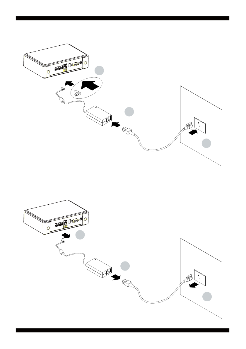
Photo 1 Insert
1
2
3
Unplug
3
2
1
3
Page 9

Chapter-1
General Information
The 3I770A/CW is All-In-One board which could apply to the use of Networking, POS
or Automation Control Board. It is designed to combine all necessary input and output
affects interfaces, which makes it to be ideal All-In-One control board for the demand of
Networking, POS and Automation Control applications.
High-performance and power-efficient communication platform, the embedded
motherboard of 3I770A/CW is specially designed for advanced POS systems where the
economical use of power is in high demand. Also, the high performing 3I770A/CW comes
with a DDR3 1333/1600 MHz SO-DIMM slot with up to 8GB memory and fi ve SATA ports
which include PCIe mini card sockets. This motherboard will ensure the high performance
levels required for today's most popular POS/Automation control applications including
POS, ATM, and Panel PC applications.
3I770A/CW has Intel LAN chipset with 10/100/1000 Mbps Ethernet for seamless
broadband connectivity. With the Wake-On LAN function and the PXE function in BIOS for
Intel LAN chipset, it is perfect control board for networking devices
3I770A/CW also supports with six COM ports of RS232/422/485 (optional) to meet the
needs of connectivity for multiple COM ports. In addition, there are multi-ports of HiSpeed USB 3.0/2.0 to enhance the host controller interface which will ensure the high
performance level and fl exible expansion. A single Flash chip holds the system BIOS, so
you can change the Flash BIOS by the Utility Update.
The supported display interfaces include VGA, LVDS touch screen and HDMI. With a small
footprint of only 146 x 102 mm (3.5 inch) and advanced performance in both computing
and graphics, this board meets the requirement of system developers in the gaming, POS,
digital signage, and server market segment.
4
Page 10

1-1 Major Feature
1. The Mobile Ivy Bridge processor includes Integrated Display Engine,
GPU and Integrated Memory Controller and is designed for mobile,
the processor is designed for the Chief River platform and may be offered in
a rPGA998B package
2. Intel Panther Point Platform Controller Hub (PCH) QM77 and Integrated Graphic Chip
3. Support 1 x DDR3 SO-DIMM socket (up to 8GB)
4. On board SSD fl ash memory 2/4/8/16/32/64 GB (option)
5. Support 2 x Intel GbE LAN
6. 18/24 bits dual channel LVDS Interface on Board
7. Support 2 x SATA connectors (1 x SATA 2.0 and 1 x SATA 3.0)
8. Support 2 x PCIe mini card, 1 x Half size PCIe Mini card for mSATA and USB interface,
1 x Full size PCIe Mini card for PCIe x1 or mSATA and USB interface
9. 1 x SIM card socket for 3G mini card use
10. Support 6 x Serial ports : COM3 for RS232/422/485, COM1,2,4,5,6
for RS232 or 422 or 485
11. Wide range DC input from +9V to +36V(±1V) (3I770CW)
12. Compact PCB Dimension: 146 x 102 mm (3.5 inch)
13. USB interface (full speed sample rate maximum of 300 point per second)
Touch screen controller, support 4-, 5-, 8- wire Analog Resistive touch screen,
Resolution is up to 2048 x 2048 (3I770CW)
14. Support 2 x external USB 3.0/2.0 & 2 x external USB2.0 & 5 x internal USB 2.0 ports
5
Page 11

1-2 Specifi cation
1. CPU: Intel Mobile Ivy Bridge processor in rPGA988B package
2. Chipset: Intel Panther Point Platform Controller Hub (PCH) QM77
3. Memory: 1 x DDR3 SO-DIMM socket (up to 8GB),
data transfer rates of 1333 MT/s and 1600 MT/s
4. Graphics: Integrated with Intel Mobile Ivy Bridge Processor
5. SIO and UARTs: Fintek F71869A and F81216AD I/O chipset
6. On board SATA SSD 2/4/8/16/32/64 GB (Option)
7. SATA: 2 x SATA ports (1 x SATA 2.0 and 1 x SATA 3.0)
8. LAN Interface: One Intel 82579LM GbE LAN PHY and one Intel 82574L GbE LAN
9. Serial Port: 5 x RS232 or 422 or 485 + 1 x RS485/422/232
10. USB: 2 x external USB 3.0/2.0 & 2 x external USB 2.0 & 5 x internal USB2.0
11. Sound: Intel HD Audio Specifi cation Two channel sound
12. LVDS: 18/24bits, 2ch
13. WDT / DIO: Hardware watch dog timer support, 0~255 sec programmable
14. Hardware digital Input & Output, 8 x DI / 8 x DO
15. Touch screen: C8051F321 USB interface touch screen controller,
support 4-, 5-, 8- wire Analog resistive touch screen,
Resolution is up to 2048 x 2048 (3I770CW)
16. Audio Amplifi er: Ti TPA2011D1 Class D 2.5W Audio amplifi er
17. Expansion interface: 1 x Half size PCIe Mini card for mSATA and USB interface,
1 x Full size PCIe Mini card for PCIe x1 or mSATA and USB interface
18. BIOS: AMI UEFI BIOS
19. Dimension: 146 x 102 mm (3.5 inch)
20. Power: Wide range DC input from +9V to +36V(±1V) (3I770CW)
Onboard DC-in Convert into system power +12VAD to +5V/±5% and +3.3V/±5%
and +12V/±5%
21. 1 x 3G SIM card socket
6
Page 12
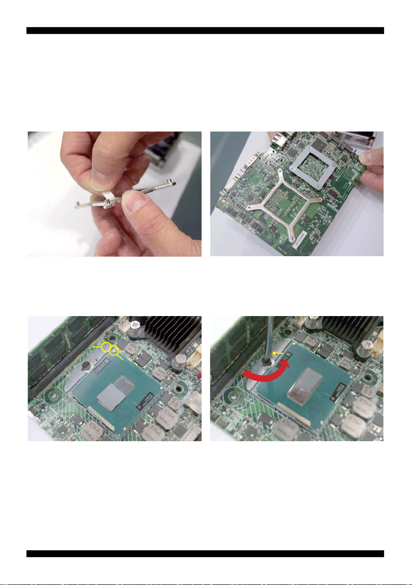
1-3 Installing the CPU / PCH Heatsink. (Socket Version)
1. Remove the white wax paper from the
double-sided-adhesive-tap of the
CPU Barcket
3.1. Locate Pin1 in the socket,look for a
golden narrow.
Golden arrow
Socket Pin1
2. Install CPU bracket under the CPU fi rst.
3.2. Use screw driver and screw the socket
screw in anti-clockwise direction.
Socket screw
7
Page 13
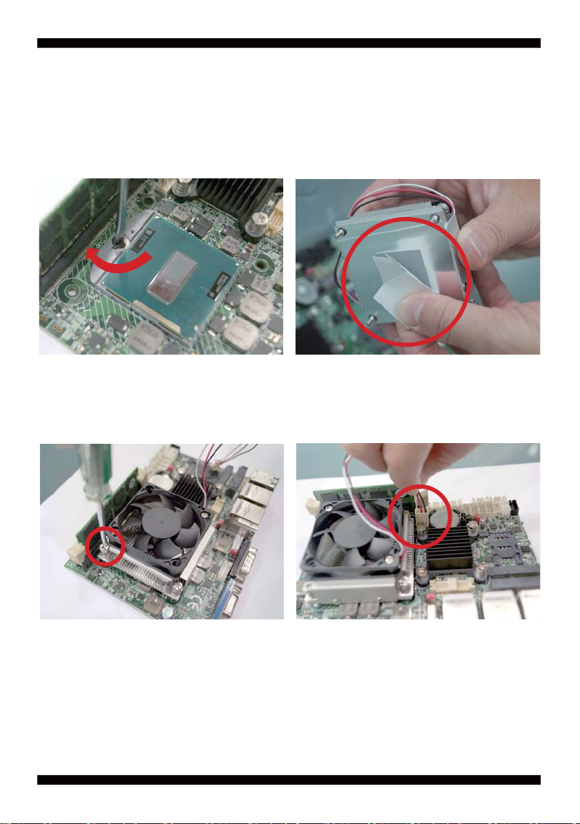
3.3. Lock the CPU socket by securing the
screw in an anti-clockwise direction.
4. Peel-off the Elastic Silicone sticker
under the Heat Sink.
4.1. Tighten the HEAT SINK on the
motherboard. Pay attention to tighten the
screws diagonally.
4.2. Insert the system fan power cable to
the pin header (FAN1) on board.
8
Page 14
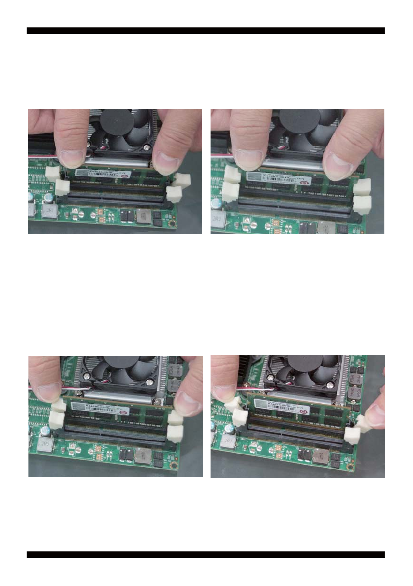
1-4 Vertical SO-DIMM assembly guide
1. Install the memory into SODIMM. 2. Press down fi rmly to ensure the memory
is locked.
------------------------------------------------------------------------------------------------------------------------
Uninstall
1. Pull open both sides of the memory slot. 2. Take out the memory.
9
Page 15
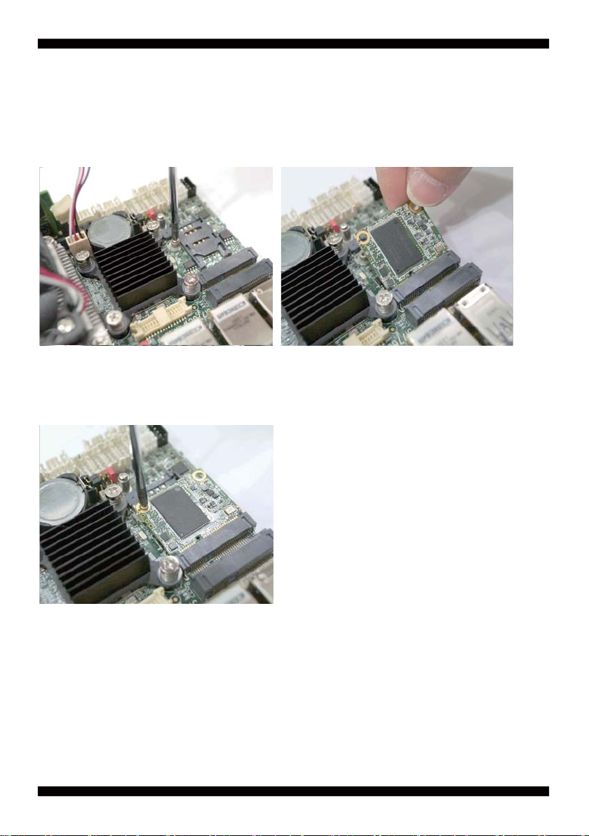
1-5 Installing the Mini PCI-e Card
1. Unfasten the round-headed M2*6
screw for half size Mini PCI-e.
3. Fasten a round-headed M2*6 screw.
2. Install a mSATA card at the angle of 45°.
(The half size Mini PCI-e slot supports mSATA)
10
Page 16
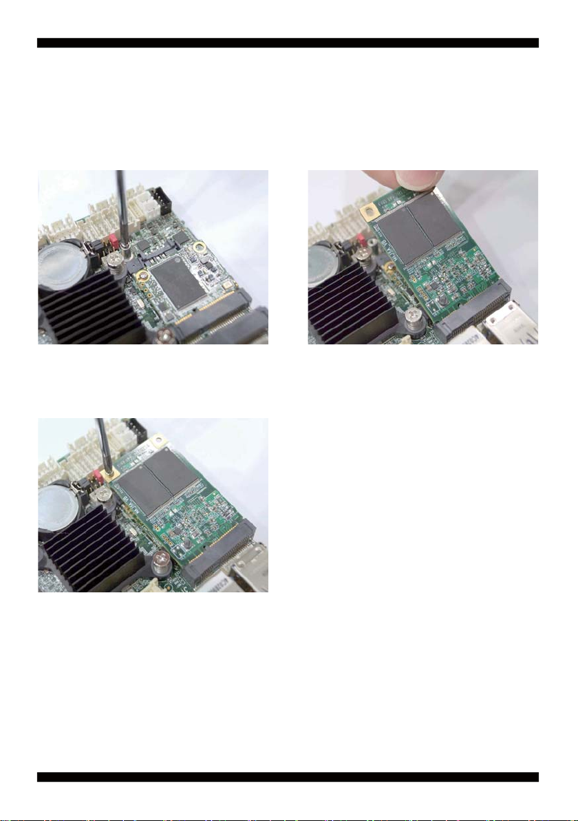
1-6 Directions for installing the Mini Card
1. Unscrew the screw on the board
3. Gently push down the Mini Card and screw the screw back.
2. Plug in the Mini Card in a 45 angle
11
Page 17
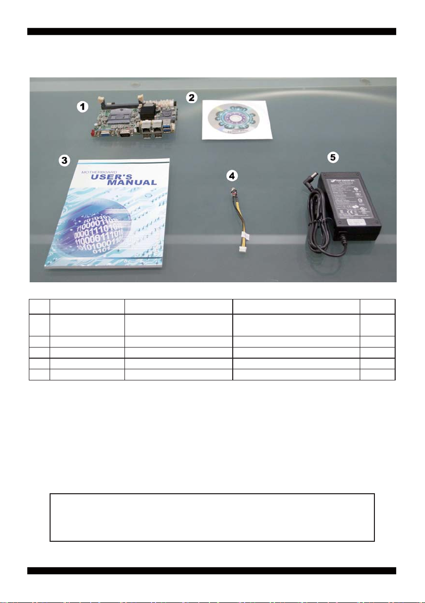
1-7 Packing List
Material Code Description Detail Specifi cation Quantit
7G1901-1510001-0
1
7G1901-1520001-0
6G8006-2347-0100 LEX Product Driver DVD LF, Intel Baytrail Driver 1
2
6G8001-2193-0400 Manual LF,M/B,3I770A/CW 1
3
6G6003-7350-0100 Power Cable LF, 2.0 2*4/DC JK,L=9cm 1
4
6G5212-0601-0200 84W Power Adapter,12V/5A,2.5 LF,L Type,FSP060-DBAE1,FSP 1
5
MB-3I770CW-6CXX-00-001
MB-3I770A-6CXX-00-001
LF,3I770CW-6CXX-00,Rev.:001
LF,3I770A-6CXX-00,Rev.:001
1
*The packing list above is for the users who purchase single motherboard. The users
who purchase the board with chassis may refer to the packing list in the Assembly Guide.
Please contact with your dealer if any of these items is missing or damaged
on delivery. And please keep all parts of the delivery package with packing
materials in case if you need to deliver or store the product in the future.
12
Page 18

Chapter-2
Hardware Installation
2-1 Unpacking Precaution
This chapter provides the information how to install the hardware of 3I770A/CW.
Please follow section 1-7, 2-1 and 2-2 to check the delivery package and unpack
carefully. Please follow the jumper setting procedure.
NOTE!
1. Do not touch the board or any other sensitive components without all necessary
anti-static protection.
2. Please pay attention to the voltage limitation of DC-IN12 V 5 %.
Overuse of DC-IN voltage limitation or change to another power adapter
( not provided with this system ) will VOID warranty.
You should follow these
steps to protect the board from the static electric
discharge whenever you handle the board:
1. Ground yourself by a grounded wrist strap at all times when you
handle the 3I770A/CW.
Well secure the ALLIGATOR clip of the strap to the end of the shielded wire lead from
a grounded object. Please put on and connect the strap before handling the
3I770A/CW for harmlessly discharge any static electricity
through the strap.
2. Please use anti-static pad to put any components, parts, or tools on the pad whenever
you work on them outside the computer. You may also use the anti-static bag instead of
the pad. Please ask your local supplier for necessary parts on anti-static requirement.
3. Do not plug any connector or set any jumper when the power is on.
13
Page 19

2-2 Unpacking checkup
First of all, please follow all necessary steps of section 2-1 to protect 3I770A/CW
from electricity discharge. With reference to section 1-7
please check the delivery package again with following steps:
1. Unpack the 3I770A/CW board and keep all
packing material, manual and driver disc etc, do not dispose !
2. Is there any components lose or drops from the board?
DO NOT CONTINUE TO INSTALL THIS BOARD!
CONTACT THE DEALER YOU PURCHASED
THIS BOARD FROM, IMMEDIATELY.
3. Is there any visible damage on the board?
DO NOT CONTINUE TO INSTALL THIS BOARD!CONTACT
THE DEALER YOU PURCHASED THIS BOARD FROM, IMMEDIATELY.
4. Check your optional parts (i.e. DDR, CF etc.), all necessary jumpers
setting to jumper pin-set, and CMOS setup correctly.
Please also refer to all information of jumper settings in this manual.
5. Check your external devices (i.e. Add-On-Card, Driver Type etc.)
for complete add-in or connection and CMOS setup correctly.
Please also refer to all information of connector connection in this manual.
6. Please keep all necessary manual and driver disc in a good condition for future
re-installation if you change your Operating System.
14
Page 20
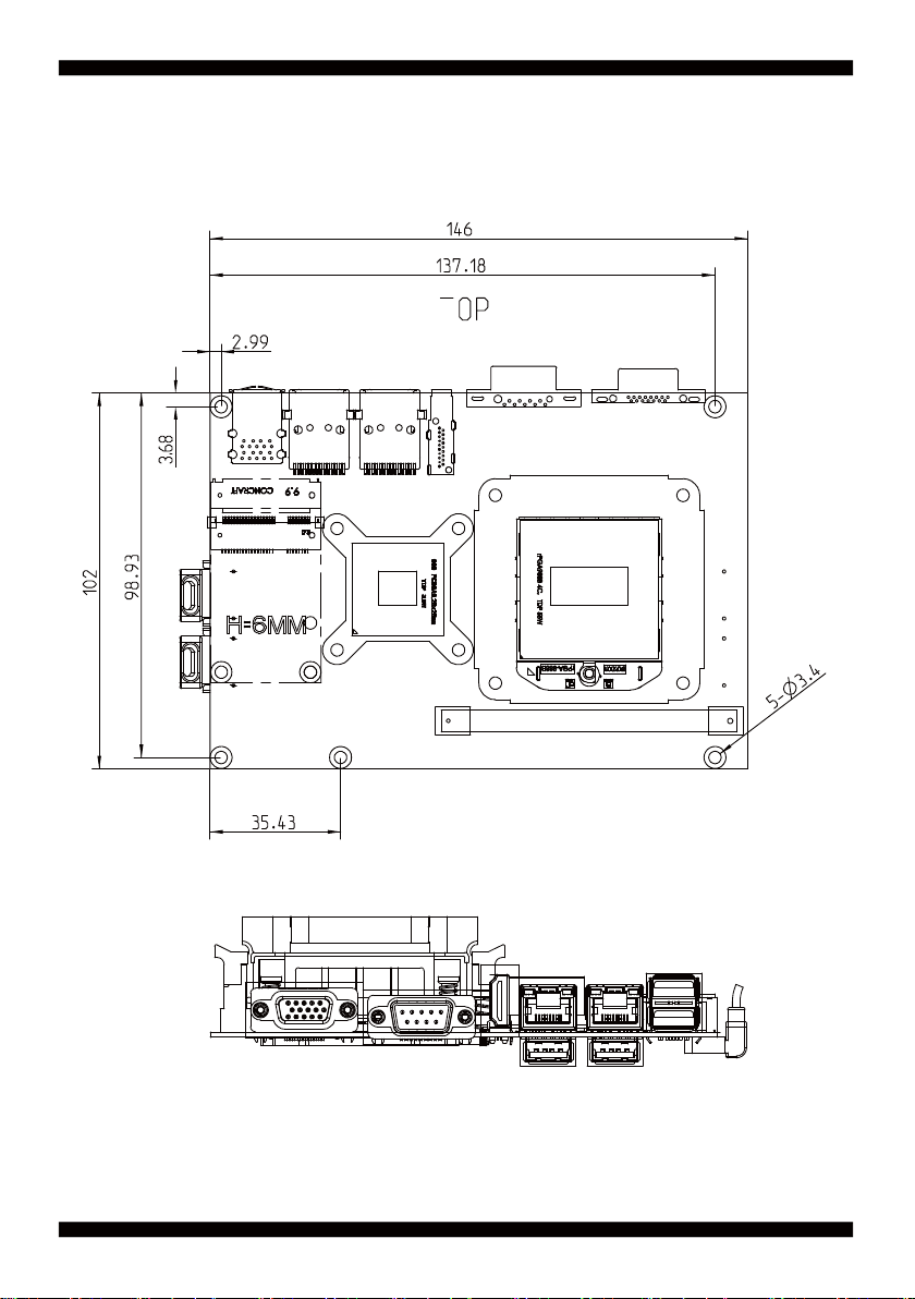
2-3 Dimension-3I770A/CW
15
Page 21
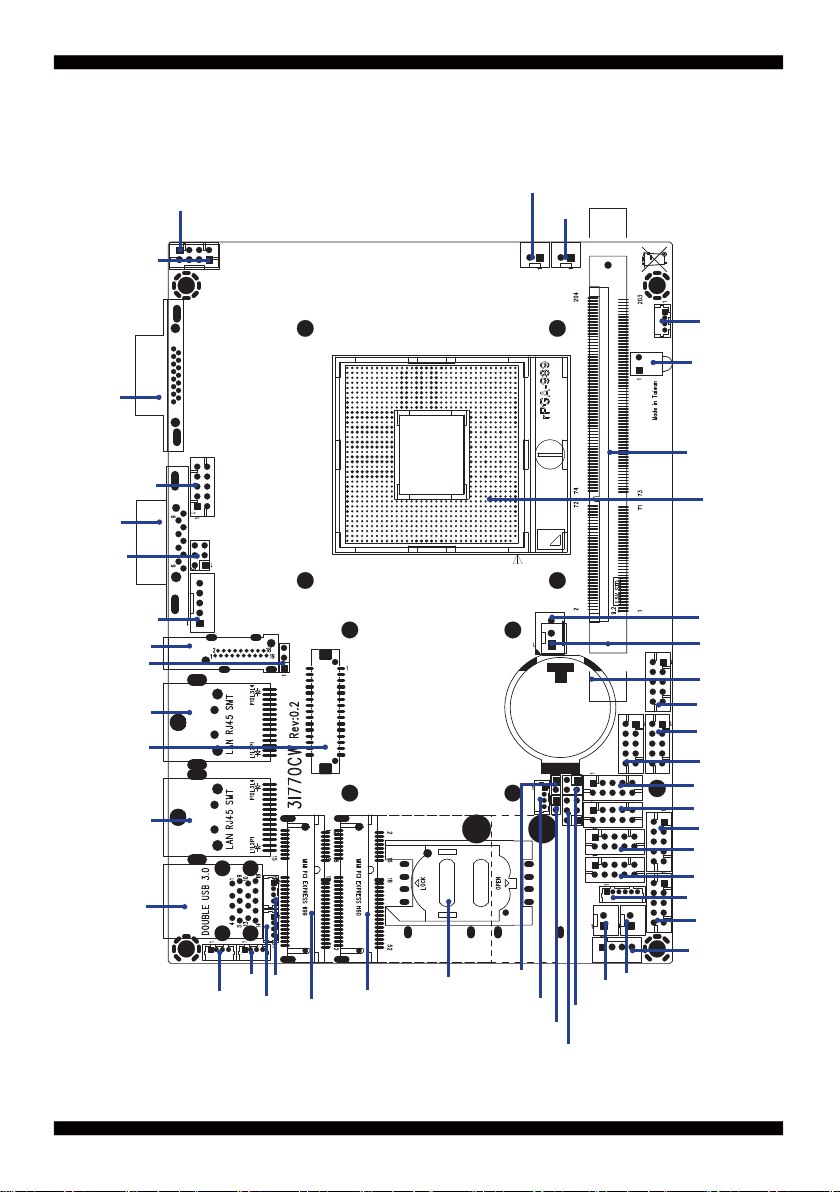
2-4 Layout-3I770A/CW
CG1
CC1
JVC1
HDMI1
LVDS1
CU12
CPI11
CC2
CPP1
JVL1
CL2
CL1
CPI1
CU3
CU4
CU7
CU8
MPCE2
MPCE1
SIM1
COH1
JSB1
CU9
JSB2
COS1
JVC3
CAR1
JSC3
CO1
LED1
SODIMM1
SK1
FAN1
CPO2
BAT1
CFP1
CC6
CC5
CC4
CC3
CA3
CIO2
CIO1
CKM1
CT1
CPO1
CAL1
16
Page 22
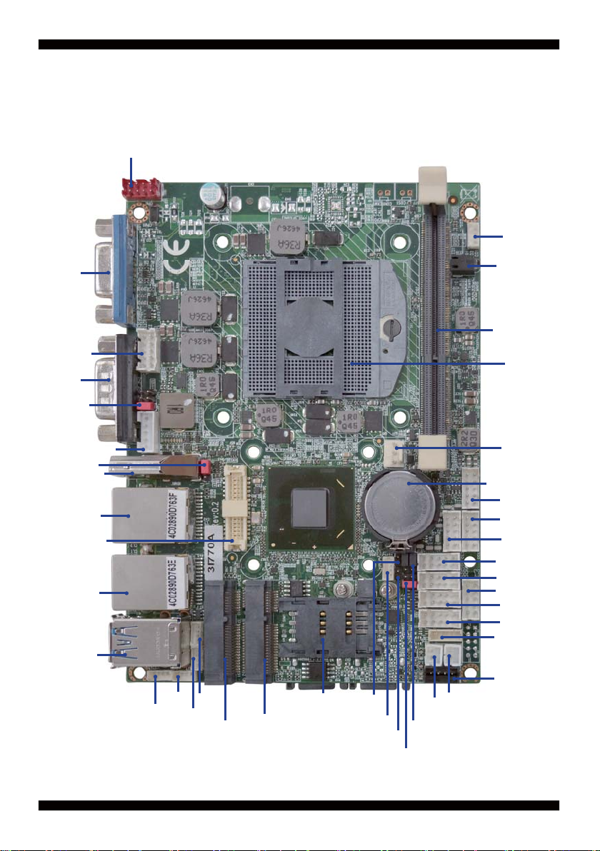
2-5 Diagram- 3I770A
CPI1
CO1
CG1
CC2
CC1
JVC1
CU12
CPP1
JVL1
HDMI1
CL2
LVDS1
CL1
CU3
CU4
CU7
CU8
MPCE2
MPCE1
SIM1
JSB1
CU9
JSB2
CAR1
JSC3
JVC3
LED1
SODIMM1
SK1
FAN1
BAT1
CFP1
CC6
CC5
CC4
CC3
CA3
CIO2
CIO1
CKM1
CPO1
CAL1
17
Page 23

2-5-1 Diagram- 3I770CW
CPI1
CO1
CG1
CC2
CC1
JVC1
JVL1
CU12
CPP1
HDMI1
CL2
LVDS1
CL1
CU3
CU4
CU7
CU8
MPCE2
MPCE1
SIM1
JSB1
CU9
JSB2
CAR1
JSC3
JVC3
LED1
SODIMM1
SK1
FAN1
BAT1
CFP1
CC6
CC5
CC4
CC3
CA3
CIO2
CIO1
CKM1
CPO1
CAL1
18
Page 24
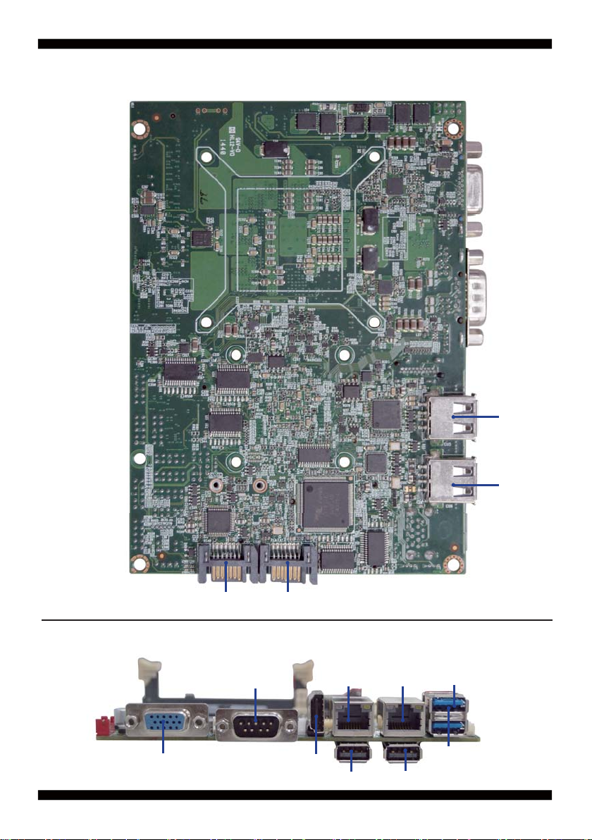
2-5-2 Bottom Side Diagram- 3I770A/CW
Side Diag
3I770A/CW
ottom
ram-
CU5
SATA 1 SATA 2
BACK Panel-3I770A/CW
VGA
COM
HDMI
19
LAN2
LAN1
USBUSB
CU6
USB
USB
Page 25

2-6 Install Memory
This motherboard provides one 204-pin Small Outline Dual In-line Memory Module (SODIMM)
socket for memory expansion available maximum to of 2GB/4GB/8GB DDR3 SDRAM.
DDR3 clock supports: DDR3 1333/1600MT/S
Valid Memory Confi gurations
Total Memory
DIMM1
System Accept or Not
Max.
DS/SS Accept
8GB
SS: Single Sided DIMMDS: Double Sided DIMM
NOTE!
The detected memory size is less than actual installed memory size since
some memory has been allocated for system use.
That’s how PC works with system memory.
Please refer to page 9 for installation of memory module.
20
Page 26
2-7 List of Jumpers
JSB1: CMOS clear select
JSB2: ME RTC clear select
JSC3: COM3 RS232/RS422/RS485 select
JVC1: COM1 voltage select
JVC3: COM3 voltage select
JVL1: LCD Panel power select
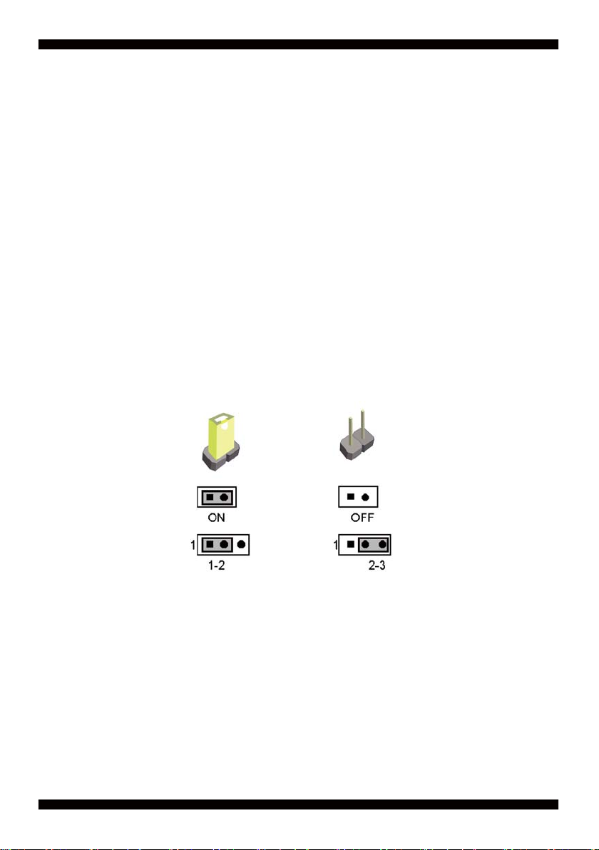
2-8 Jumper Setting Description
A jumper is ON as a closed circuit with a plastic cap covering two pins. A jumper is OFF
as an open circuit without the plastic cap. Some jumpers have three pins, labeled 1, 2,
and 3. You could connect either pin 1 and 2 or 2 and 3.The below fi gure 2.2 shows the
examples of different jumper settings in this manual.
Figure 2.2
All jumpers already have its default setting with the plastic cap inserted as ON,
or without the plastic cap as OFF. The default setting may be referred in this
manual with a " * " symbol .
21
Page 27
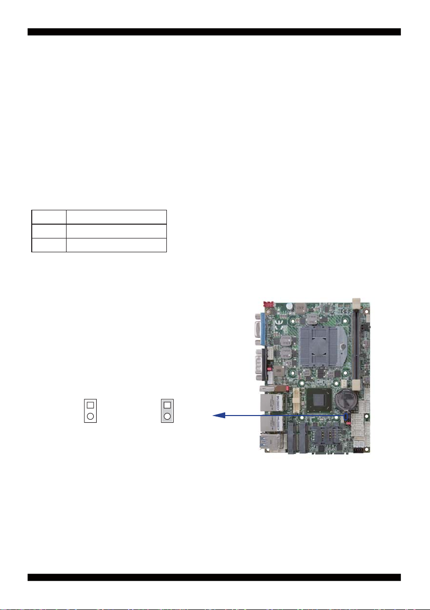
2-9 JSB1: CMOS DATA SET
A battery must be used to retain the motherboard confi guration in CMOS RAM.
Close Pin1 and pin 2 of JSB1 to store the CMOS data.
To clear the CMOS,follow the procedures below:
1. Turn off the system and unplug teh AC power
2. Remove DC IN power cable from DC IN power connector
3. Locate JSB1 and close pin 1-2 for few seconds
4. Return to default setting by openning pin 1-2
5. Connect DC IN power cable back to DC IN Power connector
JSB1 Description
*open Normal set
short CMOS data clear
Note: Normal work is open jumper
JSB1
11
22
*Normal short
Note: Do not clear CMOS unless
1. Troubleshooting
2. Forget password
3. You fail over-clocking system
22
Page 28
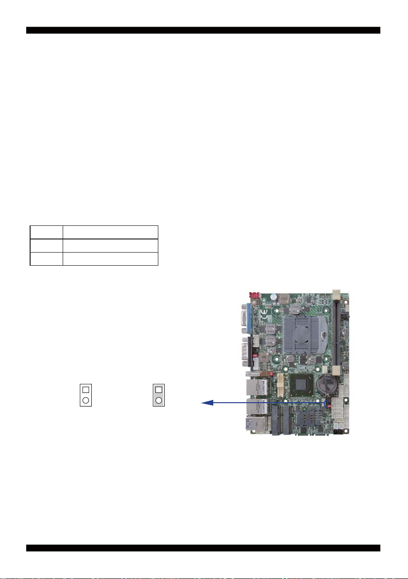
2-10 JSB2: ME RTC DATA Clear
A battery must be used to retain the motherboard confi guration in ME RAM.
Close Pin1 and pin 2 of JSB2 to store the ME data.
To clear the ME,follow the procedures below:
1. Turn off the system and unplug teh AC power
2. Remove DC IN power cable from DC IN power connector
3. Locate BAT1 and Remove Li battery
4. Locate JSB2 and close pin 1-2 for few seconds
5. Return to default setting by openning pin 1-2
6. Install Li battery to BAT1 connector
7. Connect DC IN power cable back to DC IN Power connector
JSB2 Description
*open Normal set
short CMOS data clear
Note: Normal work is open jumper
Note: Do not clear CMOS unless
1. Troubleshooting
2. Forget password
3. You fail over-clocking system
JSB2
11
22
*Normal
short
23
Page 29
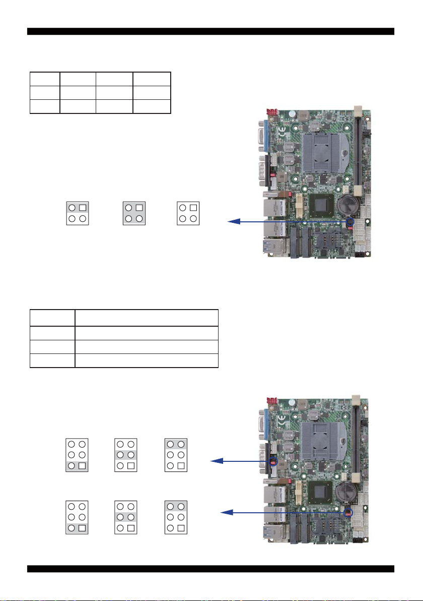
2-11 JSC3: COM3 RS232/RS422/RS485 select
JSC3 RS232 *RS422 RS485
1-2 Short Short Open
3-4 Open Short Open
Note: RS232/RS422/485 setting by both H/W jumper and
BIOS setting
JSC3
222
444
111
333
*RS422 RS485RS232
2-12 COM port pin9 select RI signal or Voltage source
JVC1: COM1 PIN9 select JVC3: COM3 PIN9 select
JVC1/3
*1-2 COM port pin9 use RI signal
3-4 COM port pin9 use +5V voltage
5-6 COM port pin9 use +12V voltage
Note: 1. Note: Attention ! Check Device Power in spec
2. If want to use +5V/+12V need check system power design spec
JVC1
6
4
2
JVC3
6
4
2
Description
5
6
3
4
1
2
5
6
3
4
1
2
5
6
3
4
1
2
5
6
3
4
1
2
5
3
1
5
3
1
*RI Signal
+5V +12V
24
Page 30

2-13 JVL1: LCD panel power select
JVL1 Description
+5V
1-2
+3.3V
*2-3
Note: Attention ! Check Device Power in spec
JVL1
33
22
11
+5V *+3.3V
25
Page 31

Chapter-3
Connection
This chapter provides all necessary information of the peripheral's connections,
switches and indicators. Always power off the board before you install the peripherals.
3-1 List of Connectors
CPI1: DC-in 2x4 pin (2.0mm) Red wafer connector
CPI11: DC-in 1x4 pin (2.0mm) Red wafer connector ( Option )
BAT1: Li 3V battery holder
CPO1: DC +5/+12V output 1x4 pin(2.0mm) Black wafer connector
CPO2: DC +12V output 1x2 pin(2.0mm) Black wafer connector ( Option )
CFP1: Front panel port 2x5 pin (2.00mm) wafer
FAN1: CPU fan 1x3 pin (2.54mm) wafer
CG1: VGA port DB15 Connector
HDMI1: HDMI type A connector
LVDS1: LVDS 2x15 pin (1.25mm) connector
CPP1: Panel inverter power connector 1x5 pin (2.0mm) wafer
CT1: Touch screen device 2x5 pin (2.0mm) Wafer
CA3: Line-out/Line-in/Mic-in 2x5 pin (2.0mm) wafer.
CAL1: Amplifi er Line-out Left channel 2pin (2.0mm) wafer
CAR1: Amplifi er Line-out Right channel 2pin (2.0mm) wafer
CC1: COM port DB15 Connector
CC2/CC3/CC4/CC5/CC6: COM 2x5pin (2.0mm) wafer
CIO1: DI port 0 ~ 3, DO port 0 ~ 3 2x5 pin (2.0mm) wafer
CIO2: DI port 4 ~ 7, DO port 4 ~ 7 2x5 pin (2.0mm) wafer
2
CO1: I C 4pin (1.25mm) wafer
CKM1: KB/MS port 1x6 pin (1.25mm) wafer connector
CL1/CL2: LAN RJ45 connector
CU5/CU6: USB port 4/5 Type A connector
CU3/CU4/CU7/CU8/CU9: USB port 2/3/12/11/13 4pin(1.25mm) wafer
CU12: Dual USB USB3.0/2.0 connector
SATA1: SATA port 0 (Gen III) connectors 7pin
SATA2: SATA port 2 (Gen II) connectors 7pin
MPCE1: Half size Mini card port 1 sockets 52pin
MPCE2: Full size Mini card port 2 sockets 52pin
SIM1: SIM port 1 card socket
SODIM1: SO-DIM DDR3 1.5V DRAM Socket
26
Page 32

3-2 DC power input
CPI1: DC-IN Internal Connector (2 X 4 pin 2.0mm Red Wafer)
PIN NO. Description PIN NO. Description
1 GND 2 GND
3 DC-IN 4 DC-IN
5 DC-IN 6 DC-IN
7 GND 8 GND
Note: 1. DC in from adapter plug in
2. Share CPI11 Connector
3. Mating connector: JST B8B-PHDSS or compatible
4. Cable housing: JST PHDR-08VS or compatible
CPI11: DC-IN Internal Connector (Option) (1 X 4 pin 2.0mm Red wafer)
PIN NO. Description
1 GND
2 DC-IN
3 DC-IN
4 GND
Note: 1. DC in from adapter plug in
2. Mating connector: JST B4B-PH-KL or compatible
3. Cable housing: JST PHR-4 or compatible
pin1
CPI11
CPI1
pin1
27
Page 33

3-3 Battery Input
BAT1: 3V Battery hold 2pin
BAT1: Battery use Li 3V / 220mAh (CR2032)
Note: 1. When board without Adaptor plug in, this
board power RTC consumption about 2.7uA
2. If adaptor always plug in RTC power consumption about 0.1uA
BAT1
3-4 DC Power output
CPO1: +12V/+5V DC voltage output (4pin 2.00mm Black Wafer)
PIN NO. Description
1 +5V
2 GND
3 GND
4 +12V*
*Note: 1. DC in +12V by switch to DC-out voltage +12V,
so DC in need stable +12V input
2. Mating connector: JST B4B-PH-KL or compatible
3. Cable housing: JST PHR-4 or compatible
CPO2
pin1
CPO1: +12V DC voltage output ( Option )
(1 X 2 pin 2.0mm Black wafer)
PIN NO. Description
1 GND
2 +12V*
*Note: 1. DC in +12V by switch to DC-out voltage +12V,
so DC in need stable +12V input
2. Share FAN1 Connector
3. Mating connector: JST B2B-PH-KL or compatible
4. Cable housing: JST PHR-2 or compatible
28
pin1
CPO1
Page 34

3-5 Front panel & FAN
CFP1 Front panel connector (2 X 5 pin 2.0mm wafer)
PIN NO. Description PIN NO. Description
1 Power button GND 2 Power button pin
3 Reset GND 4 Reset pin
5 Power LED - 6 Power LED +
7 HDD LED- 8 HDD LED+
9 LAN LED- 10 LAN LED+
*Note: 1. Mating connector: JST B10B-PHDSS or compatible
2. Cable housing: JST PHDR-10VS or compatible
FAN connectors
FAN1: CPU FAN connector (1 X 3 pin 2.5mm wafer)
PIN NO. Description
1 GND
2 +12V
3 FAN speed detect
Note: 1. DC in +12V by switch to FAN power +12V,
so DC in need stable +12V input
2. Mating connector: MOLEX 7879-3 or compatible
3. Cable housing: MOLEX 7880-3 or compatible
29
FAN1
10
pin1
pin1
CFP1
Page 35

3-6 Display & Touch interface
CG1: VGA DB15 Connector
PIN NO. Description PIN NO. Description
1 RED 2 GREEN
3 BLUE 4 NC
5 GND 6 GND
7 GND 8 GND
9 NC 10 GND
11 NC 12 DDC DATA
13 H-SYNC 14 V-SYNC
15 DDC CLOCK
HDMI1: HDMI Connector (Type A)
PIN NO. Description PIN NO. Description
1 TMDS DATA2+ 2 GND
3 TMDS DATA2- 4 TMDS DATA1+
5 GND 6 TMDS DATA1-
7 TMDS DATA0+ 8 GND
9 TMDS DATA0- 10 TMDS CLK+
11 GND 12 TMDS CLK-
13 NC 14 NC
15 DDC CLK 16 DDC DATA
17 GND 18 +5V
19 H.P. Detect
*Note: HDMI support 1.3a Spec
CG1 HDMI1
30
Page 36

LVDS1: LVDS interface (2 X 15 pin 1.25mm wafer)
PIN NO. Description PIN NO. Description
1 PWM dimming 2 +5V
3 +LCD(5V or 3.3V) 4 +LCD(5V or 3.3V)
5 Channel-1-DATA3+ 6 Channel-0-DATA3+
7 Channel-1-DATA3- 8 Channel-0-DATA3-
9 Channel-0-DATA2+ 10 Channel-0-CLK+
11 Channel-0-DATA2- 12 Channel-0-CLK-
13 GND 14 GND
15 Channel-0-DATA1+ 16 Channel-0-DATA0+
17 Channel-0-DATA1- 18 Channel-0-DATA0-
19 GND 20 GND
21 +LCD(5V or 3.3V) 22 +LCD(5V or 3.3V)
23 Channel-1-DATA2+ 24 Channel-1-CLK+
25 Channel-1-DATA2- 26 Channel-1-CLK-
27 Channel-1-DATA1+ 28 Channel-1-DATA0+
29 Channel-1-DATA1- 30 Channel-1-DATA0-
Note: 1. LVDS interface support 18/24bits two channel
2. JVL1: LVDS panel +5V/+3.3V Voltage select
3. LVDS1 PIN 1 for panel backlight active, Default active setup by DPC Control
4. Pin 1 back light dimming control. Provided 200Hz / 275Hz / 380Hz / 20KHz / 25KHz
And adjust PWM duty cycle by software program
5. Mating connector: HIROSE DF13-30DS-1.25C or compatible
6. Cable housing: HIROSE DF13-30DP-1.25V or compatible
30
LVDS1
pin1
31
Page 37

CPP1: Panel Inverter power (5pin 2.0mm wafer)
PIN NO. Description
1 +12V
2 GND
3 PWM dimming
4 ENBKL (3.3V)
5 ENBKL ( 5V )
Note: 1. JVP1 Inverter Voltage select
2. CPP1 PIN 3 and LVDS1 PIN1 is same signal.
Default active setup by DPC Control
3. Pin 3 back light dimming Control.
Provided 200Hz / 275Hz / 380Hz / 20KHz / 25KHz
And adjust PWM duty cycle by software program.
4. Mating connector: JST B5B-PH-KL or compatible
5. Cable housing: JST PHR-5 or compatible
pin1
CT1: Touch screen (2x5 pin 2.0mm wafer) Default use USB interface
For 8- wire type pin defi ne
PIN NO. Description PIN NO. Description
1 Bottom 2 Bottom Sense
3 Top Sense 4 Top
5 Right 6 Right Sense
7 Left 8 Left Sense
9 GND 10 KEY
Note: 1. For eight wire type cable Pin 3 and Pin4 need short.
2. Touch controller use USB port 8
3. Mating connector: JST B10B-PHDSS or compatible
4. Cable housing: JST PHDR-10VS or compatible
For 4- wire type pin defi ne
PIN NO. Description PIN NO. Description
1 Bottom 2 N/A
3 N/A 4 Top
5 Right 6 N/A
7 Left 8 N/A
9 GND 10 KEY
Note: 1. For four wire type cable Pin 3 and Pin4 need short.
2. Touch controller use USB port 8
3. Mating connector: JST B10B-PHDSS or compatible
4. Cable housing: JST PHDR-10VS or compatible
CPP1
pin1
10
CT1
32
Page 38

For 5- wire type pin defi ne
PIN NO. Description PIN NO. Description
1 UR(H) 2 N/A
3 Sense 4 UL(Y)
5 LR(X) 6 N/A
7 LL(L) 8 N/A
9 GND 10 N/A
Note: 1. Touch controller use USB port 8
2. Mating connector: JST B10B-PHDSS or compatible
3. Cable housing: JST PHDR-10VS or compatible
3-7 Audio interface
CA3: Line-out/Line-in/Mic-in (2 X 4 pin 2.0mm wafer)
PIN NO. Description PIN NO. Description
1 Line-out-R 2 MIC-IN
3 Line-in-R 4 GND
5 GND 6 GND
7 Line-in-L 8 NC
9 Line-out-L 10 MIC-IN
Note: 1. Mating connector: JST B10B-PHDSS or compatible
2. Cable housing: JST PHDR-10VS or compatible
Audio Amplifi er class D Two channel
2.57 W/Ch (Typ.) into a 4ΩLoad
1.46 W/Ch (Typ.) into a 8ΩLoad
CAR1: Audio Amplifi er Line out Right
(1 X 2 pin 2.0mm wafer)
PIN NO. Description
1 LINE-OUT_R+
2 LINE-OUT_R-
Note: 1. Mating connector: JST B2B-PH-KL or compatible
2. Cable housing: JST PHR-2 or compatible
CAL1: Audio Amplifi er Line out Left
(1 X 2 pin 2.0mm wafer)
PIN NO. Description
1 LINE-OUT_L+
2 LINE-OUT_L-
Note: 1. Mating connector: JST B2B-PH-KL or compatible
2. Cable housing: JST PHR-2 or compatible
33
CAR1
pin1
CAL1
Page 39

3-8 I/O Interface
COM ports (COM1~COM6 from super I/O)
COM1/2/4/5/6 default support RS232 mode
COM3 default support RS232/RS422/RS485 mode
RS232 mode ports (D-SUB 9pin)
CC1: COM1
PIN NO. Description PIN NO. Description
1 DCD 2 RXD
3 TXD 4 DTR
5 GND 6 DSR
7 RTS 8 CTS
9 RI/ Voltage
Note: 1. The Pin 9 Voltage set by JVC1 for CC1
RS485 mode ports (D-SUB 9pin)
CC1: COM1
PIN NO. Description PIN NO. Description
1 RS485 TX- 2 RS485 TX+
3NC 4NC
5 GND 6 NC
7NC 8NC
9NC
Note: 1. CC1 connector RS485 function for OEM BOM request
2. BIOS need setting to RS485 mode
RS422 mode ports (D-SUB 9pin)
CC1: COM1
PIN NO. Description PIN NO. Description
1 RS422 TX- 2 RS422 TX+
3 RS422 RX+ 4 RS422 RX-
5 GND 6 NC
7NC 8NC
9NC
Note: 1. CC1 connector RS422 function for OEM BOM request
2. BIOS need setting to RS485 mode
CC1
34
Page 40

RS232 mode ports (2 X 5 pin 2.0mm wafer)
CC2: COM2 CC3: COM3 CC4: COM4
CC5: COM5 CC6: COM6
PIN NO. Description PIN NO. Description
1 DCD 2 RXD
3 TXD 4 DTR
5 GND 6 DSR
7 RTS 8 CTS
CC2
10
9 RI/ Voltage 10 +5V
Note: 1. The Pin 9 Voltage set by JVC3 for CC3
pin1
2. Mating connector: JST B10B-PHDSS or compatible
3. Cable housing: JST PHDR-10VS or compatible
RS485 mode ports (2 X 5 pin 2.0mm wafer)
CC2: COM2 CC3: COM3 CC4: COM4
CC5: COM5 CC6: COM6
PIN NO. Description PIN NO. Description
1 RS485 TX- 2 RS485 TX+
3NC 4NC
5 GND 6 NC
7NC 8NC
9 NC 10 +5V
Note: 1. CC2/CC4/CC5/CC6 connector RS485
function for OEM BOM request
2. BIOS need setting to RS485 mode
3. Mating connector: JST B10B-PHDSS or compatible
4. Cable housing: JST PHDR-10VS or compatible
RS422 mode ports (2 X 5 pin 2.0mm wafer)
CC2: COM2 CC3: COM3 CC4: COM4
CC5: COM5 CC6: COM6
CC4
PIN NO. Description PIN NO. Description
1 RS422 TX- 2 RS422 TX+
3 RS422 RX+ 4 RS422 RX-
5 GND 6 NC
7NC 8NC
9 NC 10 +5V
Note: 1. CC2/CC4/CC5/CC6 connector RS422 function for OEM BOM request
2. BIOS need setting to RS485 mode
3. Mating connector: JST B10B-PHDSS or compatible
4. Cable housing: JST PHDR-10VS or compatible
pin1
CC6
pin1
10
CC5
CC3
10
35
Page 41

3-9 Digital Input / Output
CIO1 DIO 0 ~ 3 (2x5pin 2.0mm wafer)
PIN NO. Description PIN NO. Description
1 DI-0 2 DO-3
3 DI-1 4 DO-2
5 DI-2 6 DO-1
7 DI-3 8 DO-0
9 GND 10 +5V
Note: 1. DI pin default pull up 10KΩ to +5V
2. If use need isolate circuit to control external device
3. F75111N-1 I C bus address 0x9c
4. Mating connector: JST B10B-PHDSS or compatible
5. Cable housing: JST PHDR-10VS or compatible
CIO2 DIO 4 ~ 7 (2x5pin 2.0mm wafer)
PIN NO. Description PIN NO. Description
1 DI-4 2 DO-7
3 DI-5 4 DO-6
5 DI-6 6 DO-5
7 DI-7 8 DO-4
9 GND 10 +5V
Note: 1. DI pin default pull up 10KΩ to +5V
2. If use need isolate circuit to control external device
3. F75111N-1 I C bus address 0x9c
4. Mating connector: JST B10B-PHDSS or compatible
5. Cable housing: JST PHDR-10VS or compatible
2
2
36
pin1
CIO2
CIO1
10
Page 42

For F75111N I C watch dog timer device:
2
DC spec:
Input low Voltage (VIL)\+0.8 Max
Input High Voltage (VIH): +2V Min
Output low Current (IOL): 10mA (Min) VOL=0.4V
Output High Current (IOH): -10mA (Min) VOH=2.4V
Watch Dog Time value 0~255 sec
The system will be issued reset. When WDT is enable the hardware start down counter
to zero. The reset timer have 10~20% tolerance upon the Temperature.
Note: If want to SDK support. Please contact to sales window.
Please refer to page 82 for APPENDIX C: F75111N I C DIO DECICE
2
37
Page 43

3-10 I C Bus Interface
Note: 1. Mating connector: MOLEX 53047-0410 or compatible
2. Cable housing: MOLEX 51021-0400 or compatible
2
2
CO1: I C (SM) bus connector (4 pin 1.25mm wafer)
PIN NO. 1 2 3 4
Description +3.3V GND SMB_CLK SMB_DATA
CO1
pin1
3-11 PS2 KB/MS
CKM1: KB/MS port (1 X 6 pin 1.25mm wafer)
PIN NO. 1 2 3 4 5 6
Description +5V KB/DAT KB/CLK GND MS/DAT MS/CLK
Note: 1. Mating connector: MOLEX 53047-0610 or compatible
2. Cable housing: MOLEX 51021-0600 or compatible
pin1
CKM1
38
Page 44

CL1
C
3-12 LAN Interface
CL1 / CL2: LAN Giga/100Mb (RJ45 Jack)
PIN NO. Description PIN NO. Description
1 TD0-/TX+ 5 TD2-/NC
2 TD0+/TX- 6 TD2+/RX-
3 TD1-/RX+ 7 TD3-/NC
4 TD1+/NC 8 TD3+/NC
RJ45 LAN Connector--- LED defi ne Giga/100MB Connector
Back side con RED LED GREEN LED YELLOW LED
Indicate
GIGA LAN
Link(light)
RJ45 LAN Connector--- LED defi ne Giga/100/10MB Connector
100Mb LAN
Link(light)
Active LED
Link(Blink)
SPEED
Indicate
LAN Light
10 Mbps 100Mbps 1000 Mbps
Side
LED
Back Back BackFront Front Front
Link Link Link
Orange Orange Green Orange Orange Orange Orange
Back Red
ACT ACT ACTACT ACT ACT
L2
CL1CL2
39
Page 45

3-13 USB Interface
CU5/CU6: USB4/5 ports (USB Type A connector)
PIN NO. Description
1 +5V
2 USB DATA -
3 USB DATA +
4 GND
Note: 1. Attention ! Check Device Power in spec
CU3/CU4/CU7/CU8/CU9: USB 2/3/11/12/13 ports
PIN NO. Description
1 +5V
2 USB DATA -
3 USB DATA +
4 GND
Note: 1. Attention! Check Device Power in spec
2. Mating connector: MOLEX 53047-0410 or compatible
3. Cable housing: MOLEX 51021-0400 or compatible
CU12: Dual USB3.0/2.0 port (Type A jack)
PIN NO. Description PIN NO. Description
pin1
1 USB3.0 TX+
1 +5V
2 USB 2.0 D- 2 USB3.0 TX-
3 GND
3 USB 2.0 D+ 4 USB3.0 RX+
4 GND
5 USB3.0 RX-
Note: 1. USB 3.0 and USB 2.0 combo Type A Jack
2. USB3.0/2.0 Keyboard and Mouse use CU12 can pitch Some OS install
And wake up Keyboard and Mouse can’t work issue
pin1
CU4CU3
CU12
pin1
CU8
pin1
CU7
pin1
CU9
40
CU6CU5
Page 46

3-14 SATA interface
SATA1/SATA2: The two SATA connectors
PIN NO. Description
1 GND
2 DATA TX+
3 D ATA T X -
4 GND
5 DATA RX-
6 DATA RX+
7 GND
Note: 1. SATA1 support SATA 3.0 spec update 6Gb/sec .
2. SATA2 support SATA 2.0 spec update 3Gb/sec .
3. CPO1 provide SATA HDD power +12V, GND, +5V
SATA 1 S ATA2
SSD use at SATA3 channel
Note: 1. On board SSD for OEM option
41
Page 47

3-15 Module socket
Mini card
MPCE1/MPCE2: Support USB and PCIe by one Interface (Mini card socket 52pin)
PIN NO. Description PIN NO. Description
1 NC 2 +3.3V
3 NC 4 GND
5 NC 6 +1.5V
7 NC 8 SIM Power
9 GND 10 SIM Data
11 PCIe-CLK- 12 SIM CLK
13 PCIe-CLK+ 14 SIM Reset
15 GND 16 SIM RFU
KEY KEY KEY KEY
17 NC 18 GND
19 NC 20 NC
21 GND 22 RST-
23 PCIe-RX-/mSATA-RX+ 24 +3.3V
25 PCIe-RX+/mSATA-RX- 26 GND
27 GND 28 +1.5V
29 GND 30 SMB-CLK
31 PCIe-TX-/mSATA-TX- 32 SMB-DATA
33 PCIe-TX+/mSATA-TX+ 34 GND
35 GND 36 USB-DATA-
37 GND 38 USB-DATA+
39 +3.3V 40 GND
41 +3.3V 42 NC
43 NC 44 NC
45 NC 46 NC
47 NC 48 +1.5V
49 NC 50 GND
51 mSATA-Detect 52 +3.3V
Note: 1. MPCE1 Half size, MPCE2 Full size
2. MPCE1 used USB port 9, MPCE2 used USB port 10
3. MPCE1 Pin 8,10,12,14,16 for NC
4. MPCE1 Pin 23,25,31,33 for mSATA device Only
5. MPCE2 Pin 8, 10,12,14,16 for SIM1 card reader use
6. MPCE2 Pin23, 25, 31, 33 supported mSATA device and PCIe device alternatively
7. MPCE2 Pin51 mSATA / PCIe auto detect function
42
Page 48

3-16 SIM Socket
SIM1: SIM card socket pin defi ne is follow ISO 7816-2 smart card standard.
PIN NO. Description PIN NO. Description
1 Vcc 1 GND
2 RST 2 Vpp
3 CLK 3 DATA
4 RUF 4 RUF
Note: 1. MPCE1 Pin 8, 10,12,14,16 for SIM1 card reader use.
3-17 SODIMM socket
Note: 1.SODIM1: SO-DIM DDR3 1.5V DRAM Socket
2. Support un-buffer type module
SODIMM1
SIM1
43
Page 49

Chapter-4
Introduction of BIOS
The BIOS is a program located in the Flash Memory on the motherboard.
This program is a bridge between motherboard and operating system.
When you start the computer, the BIOS program gains control.
The BIOS fi rst operates an auto-diagnostic test called POST
(Power on Self Test) for all the necessary hardware, it detects the entire hardware
devices and confi gures the parameters of the hardware synchronization. After these tasks
are completed, BIOS will give control of the computer back to operating system (OS).
Since the BIOS is the only channel for hardware and software to communicate with, it is
the key factor of system stability and of ensuring your system performance at best.
In the BIOS Setup main menu, you can see several options. We will explain these options
in the following pages. First, let us see the function keys you may use here:
Press <Esc> to quit the BIOS Setup.
Press ↑↓←→(up, down, left, right) to choose the option you want to confi rm or modify.
Press <F10> to save these parameters and to exit the BIOS Setup menu
after you complete the setup of BIOS parameters.
Press Page Up/Page Down or +/- keys to modify the BIOS parameters for
the active option.
4-1 Enter Setup
Power on the computer and press <Del> key immediately to enter Setup.
If the message disappears before your respond but you still wish to enter Setup,
restart the system by turning it OFF then ON or You may also restart the system by
simultaneously pressing <Ctrl>, <Alt> and <Delete> keys.
44
Page 50

4-2 BIOS Menu Screen
The following diagram show a general BIOS menu screen
Main Advanced
BIOS Vendor 3I770A-C A1
Processor Information
Name IvyBridge
Brand String Intel(R) Core(TM) i7
Frequency 2300 MHz
Total Memory 8192 MB (DDR3)
Memory Frequency 1600 MHz
System Date [Tue 01/15/2013]
System Time [19:28:51]
Menu Items
Chipset
Version 2.14.1219. Copyright (C) 2011 American Megatrends, Inc.
Boot
Security
Current Setting Value
Save & Exit
Function Keys
Menu Bar
Set the date. Use Tab
to Switch between
date elements.
General Help Items
→←: Select Screen
↑↓: Select Item
Enter: Select
+/-: Change Opt.
F1: General Help
F2: Previous Values
F3: Optimized Defaults
F4: Save & Exit
Esc: Exit
4-3 Function Keys
In the above BIOS Setup main menu of, you can see several options.
We will explain these options step by step in the following pages of this chapter,
but let us fi rst see a short description of the function keys you may use here:
Press ←→ (left, right) to select screen;
●
Press ↑↓ (up, down) to choose, in the main menu, the option you want to confi rm or to modify.
●
Press <Enter> to select.
●
Press <+>/<–> keys when you want to modify the BIOS parameters for the active option.
●
[F1]: General help.
●
[F2]: Previous value.
●
[F3]: Optimized defaults.
●
[F4]: Save & Reset.
●
Press <Esc> to quit the BIOS Setup.
●
45
Page 51

4-4 Getting Help
Main Menu
The on-line description of the highlighted setup function is displayed at the top right corner
the screen.
Status Page Setup Menu/Option Page Setup Menu
Press F1 to pop up a small help window that describes the appropriate keys to use and
the possible selections for the highlighted item. To exit the Help Window, press <Esc>.
4-5 Menu Bars
There are six menu bars on top of BIOS screen:
Main To change system basic confi guration
Advanced To change system advanced confi guration
Chipset To change chipset confi guration
Boot To change boot settings
Security Password settings
Save & Exit Save setting, loading and exit options.
User can press the right or left arrow key on the keyboard to switch from menu bar.
The selected one is highlighted.
4-6 Main
Main Advanced
BIOS Vendor 3I770A-C A1
Processor Information
Name IvyBridge
Brand String Intel(R) Core(TM) i7
Frequency 2300 MHz
Total Memory 8192 MB (DDR3)
Memory Frequency 1600 MHz
System Date [Tue 01/15/2013]
System Time [19:28:51]
Chipset
Version 2.14.1219. Copyright (C) 2011 American Megatrends, Inc.
Boot
Security
Main menu screen includes some basic system information. Highlight the item and then use
the <+> or <-> and numerical keyboard keys to select the value you want in each item.
Save & Exit
Set the date. Use Tab
to Switch between
date elements.
→←: Select Screen
↑↓: Select Item
Enter: Select
+/-: Change Opt.
F1: General Help
F2: Previous Values
F3: Optimized Defaults
F4: Save & Exit
Esc: Exit
System Date
Set the Date. Please use [Tab] to switch between data elements.
System Time
Set the Time. Please use [Tab] to switch between data elements.
46
Page 52

4-7 Advanced
Main Advanced
►ACPI Settings
►S5 RTC Wake Setting
►Trusted Computing
►CPU Confi guration
►SATA Confi guration
►SMART Setting
►F71869 Super IO Confi guration
►F71869 H/W Monitor
►F81216 Second Super IO Confi guration
►Serial Port Console Redirection
►Network Stack
ACPI Settings
Please refer section 4-7-1
S5 RTC Wake Setting
Please refer section 4-7-2
Trusted Computing ( For TPM OEM Function )
Please refer section 4-7-3
CPU Confi guration
Please refer section 4-7-4
Chipset
Version 2.14.1219. Copyright (C) 2011 American Megatrends, Inc.
Boot
Security
Save & Exit
System ACPI
Parameters.
→←: Select Screen
↑↓: Select Item
Enter: Select
+/-: Change Opt.
F1: General Help
F2: Previous Values
F3: Optimized Defaults
F4: Save & Exit
Esc: Exit
SATA Confi guration
Please refer section 4-7-5
SMART Settings
Please refer section 4-7-6
F71869 Super IO Confi guration
Please refer section 4-7-7
F71869 H/W Monitor
Please refer section 4-7-8
F81216 Second Super IO Confi guration
Please refer section 4-7-9
Serial Port Console Redirection
Please refer section 4-7-10
Network Stack
Please refer section 4-7-11
47
Page 53

4-7-1 ACPI Settings
Main Advanced
ACPI Settings
Enable ACPI AUTO Confi guration [Disabled]
Enable Hibernation [Enabled]
ACPI Sleep State [S1 only(CPU Stop C..)]
Chipset
Version 2.14.1219. Copyright (C) 2011 American Megatrends, Inc.
Boot
Security
Save & Exit
Enables or Disables
BIOS ACPI Auto
Confi guration.
→←: Select Screen
↑↓: Select Item
Enter: Select
+/-: Change Opt.
F1: General Help
F2: Previous Values
F3: Optimized Defaults
F4: Save & Exit
Esc: Exit
Enable ACPI Auto Confi guration
This item allows you to Enabled/Disabled the Advanced Confi guration and Power
Management (ACPI).
Enable Hibernation
This item allows you to Enabled/Disabled the Hibernate feature.
ACPI Sleep State
Select ACPI sleep state the system will enter when the SUSPEND button is pressed.
The optional settings: Suspend Disabled / S1 only(CPU Stop Clock) / S3 only(Suspend to RAM) /
Both S1 and S3 available for OS choose from.
48
Page 54

4-7-2 S5 RTC Wake Settings
Main Advanced
Wake system with Fixed Time [Disabled]
Chipset
Version 2.14.1219. Copyright (C) 2011 American Megatrends, Inc.
Boot
Security
Wake system with Fixed Time
Use this item to Enable or Disable system wake on alarm event. When set as Enabled,
system will wake on the hour/min/sec specifi ed.
Save & Exit
Enable or disable
System wake on alarm
event when enabled.
System will wake on the
hr : min : sec specifi ed
→←: Select Screen
↑↓: Select Item
Enter: Select
+/-: Change Opt.
F1: General Help
F2: Previous Values
F3: Optimized Defaults
F4: Save & Exit
Esc: Exit
4-7-3 Trusted Computing ( For TPM OEM Function )
Main Advanced
Confi guration
Security Device Support [Disabled]
Current Status Information
Chipset
Version 2.14.1219. Copyright (C) 2011 American Megatrends, Inc.
Boot
Security
Save & Exit
Enables or Disables
BIOS support for
security device.O.S.
will not show Security
Device. TCG EFI
protocol and INT1A
interface will not be
available.
→←: Select Screen
↑↓: Select Item
Enter: Select
+/-: Change Opt.
F1: General Help
F2: Previous Values
F3: Optimized Defaults
F4: Save & Exit
Esc: Exit
Security Device Support
Use this item to select Enables or Disables BIOS support for security device. O.S. will not show
Security Device. TCG EFI protocol and INT1A interface will not be available.
* The item for functions OEM.
49
Page 55

4-7-4 CPU Confi guration
Main Advanced
CPU Confi guration
Intel(R) Core(TM) i7-3610QE CPU @ 2.30GHz
CPU Signature 306a9
Microcode Path 10
Max CPU Speed 2300 MHz
Min CPU Speed 1200 MHZ
CPU Speed 2300 MHZ
Processor Cores 4
Intel HT Technology Supported
Intel VT-x Technology Supported
Intel SMX Technology Supported
64-bit Supported
L1 Data Cache 32 KB x 4
L1 Code Cache 32 KB x 4
L2 Cache 256 KB x 4
L3 Cache 6144 KB
Hyper-threading [Enabled]
Active Processor Cores [All]
Execute Disable Bit [Enabled]
Intel Virtualization Technology [Disabled]
Chipset
Version 2.14.1219. Copyright (C) 2011 American Megatrends, Inc.
Boot
Security
Save & Exit
Enabled for Windows
XP and Linux
(OS optimized for Hyperthreading Technology)
and Disabled for other
OS (OS not optimized
for Hyper-threading
Technology).
When Disabled only one
thread per enabled core
is enabled.
→←: Select Screen
↑↓: Select Item
Enter: Select
+/-: Change Opt.
F1: General Help
F2: Previous Values
F3: Optimized Defaults
F4: Save & Exit
Esc: Exit
Hyper-threading
Use this item to select Enabled for Windows XP and Linux (OS optimized for Hyper-threading
Technology) and Disabled for other OS (OS not optimized for Hyper-threading Technology). When
Disabled only one thread per enabled core is enabled.
Active Processor Cores
Use this item to select number of cores to enable in each processor package.
Execute Disable Bit
XD can prevent certain classes of malicious buffer overfl ow attacks when combined with a supporting
OS (Windows Server 2003 SP1, Windows XP SP2, SuSE Linux 9.2, RedHat Enterprise 3 Update 3.)
The optional settings are: Disabled, Enabled.
Intel Virtualization Technology
When set as Enabled, a VHM can utilize the additional hardware capabilities provided
by Vanderpool Technology.
The optional settings: Enabled, Disabled.
50
Page 56

4-7-5 SATA Confi guration
Main Advanced
SATA Controller(s) [Enabled]
SATA Mode Selection [IDE]
SATA Controller(s)
Use this item to Enable or Disable SATA Device.
SATA Mode Selection
Determine how SATA controller(s) operate.
The optional settings are: IDE Mode, AHCI Mode.
Chipset
Version 2.14.1219. Copyright (C) 2011 American Megatrends, Inc.
Boot
Security
4-7-5-1 SATA Mode Selection - AHCI Mode
Main Advanced
SATA Controller(s) [Enabled]
SATA Mode Selection [AHCI]
SATA Controller Speed [Gen3]
►Software Feature Mask Confi guration
SATA Controller Speed
Indicates the maximum speed the SATA controller can support.
The optional settings: Gen1, Gen2, Gen3.
Software Feature Mask Confi guration
Please refer section 4-7-5-1-1
Chipset
Version 2.14.1219. Copyright (C) 2011 American Megatrends, Inc.
Boot
Security
Save & Exit
Enable or disable SATA
Device.
→←: Select Screen
↑↓: Select Item
Enter: Select
+/-: Change Opt.
F1: General Help
F2: Previous Values
F3: Optimized Defaults
F4: Save & Exit
Esc: Exit
Save & Exit
Enable or disable SATA
Device.
→←: Select Screen
↑↓: Select Item
Enter: Select
+/-: Change Opt.
F1: General Help
F2: Previous Values
F3: Optimized Defaults
F4: Save & Exit
Esc: Exit
51
Page 57

4-7-5-1-1 ►Software Feature Mask Confi guration
Main Advanced
RAID0 [Enabled]
RAID1 [Enabled]
Chipset
Version 2.14.1219. Copyright (C) 2011 American Megatrends, Inc.
Boot
Security
RAID0,RAID1,RAID10,RAID5
Enable or disable RAID0, RAID1 feature.
The optional settings: Enabled, Disabled.
Save & Exit
4-7-5-2 SATA Mode Selection - RAID Mode
Main Advanced
SATA Controller(s) [Enabled]
SATA Mode Selection [RAID]
SATA Controller Speed [Gen3]
►Software Feature Mask Confi guration
Alternate ID [Disabled]
Chipset
Version 2.14.1219. Copyright (C) 2011 American Megatrends, Inc.
Boot
Security
SATA Controller(s)
SATA Mode Selection
SATA Controller Speed
►Software Feature Mask Confi guration
Please refer section 4-7-5-1-1
Alternate ID
Report alternate Device ID
The optional settings: Enabled, Disabled.
Save & Exit
Enable or disable RAID0
feature.
→←: Select Screen
↑↓: Select Item
Enter: Select
+/-: Change Opt.
F1: General Help
F2: Previous Values
F3: Optimized Defaults
F4: Save & Exit
Esc: Exit
Enable or disable SATA
Device.
→←: Select Screen
↑↓: Select Item
Enter: Select
+/-: Change Opt.
F1: General Help
F2: Previous Values
F3: Optimized Defaults
F4: Save & Exit
Esc: Exit
52
Page 58

4-7-6 SMART Settings
Main Advanced
Smart Settings
Smart Self Test [Disabled]
SMART Self Test
Run Smart Self Test on all HDDs during POST.
The optional settings are: Disabled, Enabled.
Chipset
Version 2.14.1219. Copyright (C) 2011 American Megatrends, Inc.
Boot
Security
4-7-7 F71869 Super IO Confi guration
Main Advanced
F71869 Super IO Confi guration
F71869 Super IO Chip F71869
►Serial Port 1 Confi guration
►Serial Port 2 Confi guration
Power Failure [Keep last state]
Serial Port 1 Confi guration
Please refer section 4-7-7-1
Chipset
Version 2.14.1219. Copyright (C) 2011 American Megatrends, Inc.
Boot
Security
Save & Exit
Run SMART Self Test on
all HDDs during POST.
→←: Select Screen
↑↓: Select Item
Enter: Select
+/-: Change Opt.
F1: General Help
F2: Previous Values
F3: Optimized Defaults
F4: Save & Exit
Esc: Exit
Save & Exit
Set Parameters of Serial
Port 0(COMA)
→←: Select Screen
↑↓: Select Item
Enter: Select
+/-: Change Opt.
F1: General Help
F2: Previous Values
F3: Optimized Defaults
F4: Save & Exit
Esc: Exit
Serial Port 2 Confi guration
Please refer section 4-7-7-1
Power Failure
This item specifi es whether your system will reboot after a power failure or interrupt occurs.
[Keep last state] Restores the system to the status before power failure or interrupt occurred.
[Bypass mode] Restores the system to the bypass mode.
[Always on] Leaves the computer in the power on state.
[Always off] Leaves the computer in the power off state.
53
Page 59

4-7-7-1
Main Advanced
Serial Port 1~2 Confi guration
Serial Port [Enabled]
Device Settings IO=3F8h; IRQ=4;
Change Settings [AUTO]
►Serial Port 1 Confi guration & Serial Port 2 Confi guration
Chipset
Version 2.14.1219. Copyright (C) 2011 American Megatrends, Inc.
Boot
Security
Serial Port
Use this item to enable or disable serial port (COM).
The optional settings are: Enabled, Disabled.
Change Settings
Use this item to select an optimal setting for super IO device.
The optional settings are:
AUTO
IO=3F8h; IRQ=4;
IO=3F8h; IRQ=3,4,5,6,7,10,11,12;
IO=2F8h; IRQ=3,4,5,6,7,10,11,12;
IO=3E8h; IRQ=3,4,5,6,7,10,11,12;
IO=2E8h; IRQ=3,4,5,6,7,10,11,12;
Save & Exit
Enable or Disable Serial
Port (COM)
→←: Select Screen
↑↓: Select Item
Enter: Select
+/-: Change Opt.
F1: General Help
F2: Previous Values
F3: Optimized Defaults
F4: Save & Exit
Esc: Exit
4-7-8 F17869 H/W Monitor
F17869 H/W Monitor
Press [Enter] to view PC health status.
This section shows the status of your CPU, Fan, and overall system.
This is only available when there is Hardware Monitor function onboard.
54
Page 60

4-7-9 F81216 Second Super IO Confi guration
Main Advanced
F81216 Second Super IO Confi guration
F81216 Second Super IO Chip F81216 SecondIO
►Serial Port 3 Confi guration
►Serial Port 4 Confi guration
►Serial Port 5 Confi guration
►Serial Port 6 Confi guration
Chipset
Version 2.14.1219. Copyright (C) 2011 American Megatrends, Inc.
Boot
Security
Serial Port 3 Confi guration
Please refer section 4-7-9-1
Serial Port 4 Confi guration
Please refer section 4-7-9-1
Serial Port 5 Confi guration
Please refer section 4-7-9-1
Serial Port 6 Confi guration
Please refer section 4-7-9-1
Save & Exit
Set Parameters of Serial
Port 3(COMC)
→←: Select Screen
↑↓: Select Item
Enter: Select
+/-: Change Opt.
F1: General Help
F2: Previous Values
F3: Optimized Defaults
F4: Save & Exit
Esc: Exit
4-7-9-1 Serial Port 3~6 Confi guration
Main Advanced
Serial Port 3~6 Confi guration
Serial Port [Enabled]
Device Settings IO=260h; IRQ=11;
Change Settings [AUTO]
COM3 422/485 control fl ow [Disabled]
Chipset
Version 2.14.1219. Copyright (C) 2011 American Megatrends, Inc.
Boot
Security
55
Save & Exit
Enable or Disable Serial
Port (COM)
→←: Select Screen
↑↓: Select Item
Enter: Select
+/-: Change Opt.
F1: General Help
F2: Previous Values
F3: Optimized Defaults
F4: Save & Exit
Esc: Exit
Page 61

Serial Port
Use this item to enable or disable serial port (COM).
The optional settings are: Enabled, Disabled.
Change Settings
Use this item to select an optimal setting for super IO device.
The optional settings are:
AUTO
IO=260h; IRQ=11;
IO=260h; IRQ=10,11,12;
IO=268h; IRQ=10,11,12;
IO=270h; IRQ=10,11,12;
IO=278h; IRQ=10,11,12;
COM3 422/485 control fl ow
Use this item to enable or disable serial port Auto fl ow (COM).
The optional settings are: Enabled, Disabled.
4-7-10 Serial Port Console Redirection
Main Advanced
Console Redirection [Disabled]
►Console Redirection Settings
Chipset
Version 2.14.1219. Copyright (C) 2011 American Megatrends, Inc.
Boot
Security
Save & Exit
Console Redirection
Enable or Disable.
→←: Select Screen
↑↓: Select Item
Enter: Select
+/-: Change Opt.
F1: General Help
F2: Previous Values
F3: Optimized Defaults
F4: Save & Exit
Esc: Exit
Console Redirection
Use this item to enable or disable Console Redirection.
The optional settings are: Enabled, Disabled.
56
Page 62

4-7-11 Network Stack
Main
Network stack [Disabled Link]
Network Stack
Enable/Disable UEFI network stack.
The optional settings are: Disable Link, Enable.
Advanced
Chipset
Version 2.14.1219. Copyright (C) 2011 American Megatrends, Inc.
Boot
Security
Save & Exit
4-8 Chipset
Main
►PCH-IO Confi guration
►System Agent (SA) Confi guration
Advanced
Chipset
Boot
Security
Save & Exit
Enable/Disable UEFI
network stack.
→←: Select Screen
↑↓: Select Item
Enter: Select
+/-: Change Opt.
F1: General Help
F2: Previous Values
F3: Optimized Defaults
F4: Save & Exit
Esc: Exit
PCH Parameters
Version 2.14.1219. Copyright (C) 2011 American Megatrends, Inc.
PCH-IO Confi guration
Please refer section 4-8-1
System Agent (SA) Confi guration
Please refer section 4-8-2
→←: Select Screen
↑↓: Select Item
Enter: Select
+/-: Change Opt.
F1: General Help
F2: Previous Values
F3: Optimized Defaults
F4: Save & Exit
Esc: Exit
57
Page 63

4-8-1 ►PCH-IO Confi guration
Main
Intel PCH SKU Name QM77
Intel PCH Rev ID 04/C1
Advanced
Chipset
Boot
Security
Save & Exit
PCI Express
Confi guration settings
►PCI Express Confi guration
►USB Confi guration
►PCH Azalia Confi guration
Wake on LAN [Disabled]
Version 2.14.1219. Copyright (C) 2011 American Megatrends, Inc.
PCI Express Confi guration
Please refer section 4-8-1-1
USB Confi guration
Please refer section 4-8-1-2
PCH Azalia Confi guration
Please refer section 4-8-1-3
Wake on LAN
Use this item to enable or disable integrated LAN to wake the system.
4-8-1-1 ►PCI Express Confi guration
Main
PCI Express Confi guration
►Mini PCIe 1
►Mini PCIe 2
Advanced
Chipset
Version 2.14.1219. Copyright (C) 2011 American Megatrends, Inc.
Boot
Security
Save & Exit
→←: Select Screen
↑↓: Select Item
Enter: Select
+/-: Change Opt.
F1: General Help
F2: Previous Values
F3: Optimized Defaults
F4: Save & Exit
Esc: Exit
PCI Express
Confi guration settings
→←: Select Screen
↑↓: Select Item
Enter: Select
+/-: Change Opt.
F1: General Help
F2: Previous Values
F3: Optimized Defaults
F4: Save & Exit
Esc: Exit
Mini PCIe 1
Please refer section 4-8-1-1-1
Mini PCIe 2
Please refer section 4-8-1-1-1
58
Page 64

4-8-1-1-1 ►Mini PCIe 1/2
Main
PCI Express Root Port 3/4 [Enabled]
PCIe Speed [Gen1]
PCI Express Root Port 3/4
Control the PCI Express Root Port.
The optional settings are: Enabled, Disabled.
PCIe Speed
Select PCI Express port speed.
The optional settings are: Auto, Gen1, Gen2.
Advanced
Chipset
Version 2.14.1219. Copyright (C) 2011 American Megatrends, Inc.
Boot
Security
Save & Exit
4-8-1-2 ►USB Confi guration
Main
USB Confi guration
XHCI Pre-Boot Driver [Enabled]
xHCI Mode [Auto]
HS Port #1 Switchable [Enabled]
HS Port #2 Switchable [Enabled]
HS Port #3 Switchable [Enabled]
HS Port #4 Switchable [Enabled]
xHCI Streams [Enabled]
EHCI1 [Enabled]
EHCI2 [Enabled]
XHCI Pre-Boot Driver
Use this item to enable or disable XHCI Pre-Boot Driver Support.
xHCI Mode
Mode of operation of xHCI controller.
The optional settings are: Smart Auto, Enabled, Disabled.
Advanced
Chipset
Version 2.14.1219. Copyright (C) 2011 American Megatrends, Inc.
Boot
Security
Save & Exit
PCI Express Root Port 3
Setting.
→←: Select Screen
↑↓: Select Item
Enter: Select
+/-: Change Opt.
F1: General Help
F2: Previous Values
F3: Optimized Defaults
F4: Save & Exit
Esc: Exit
Enable or disable XHCI
Pre-Boot Driver support.
→←: Select Screen
↑↓: Select Item
Enter: Select
+/-: Change Opt.
F1: General Help
F2: Previous Values
F3: Optimized Defaults
F4: Save & Exit
Esc: Exit
59
Page 65

HS Port #1 Switchable
HS Port #2 Switchable
HS Port #3 Switchable
HS Port #4 Switchable
Always for HS port switching between xHCI and EHCI. If disabled,
port is routed to EHCI. If HS port is routed to xHCI, the corresponding SS port is enabled.
The optional settings are: Disabled, Enabled.
xHCI Streams
Use this item to enable or disable xHCI Maximum Primary Stream Array Size.
The optional settings are: Disabled, Enabled.
EHCI1/ EHCI2
Use this item to enable or disable USB EHCI (USB 2.0) support.
One EHCI controller must always be enabled.
The optional settings are: Enabled, Disabled.
4-8-1-3 ►PCH Azalia Confi guration
Main Advanced
PCH Azalia Congiguration
Azalia [Auto]
Azalia Internal HDMI Codec [Enabled]
Azalia HDMI Codec [Enabled]
Chipset
Version 2.14.1219. Copyright (C) 2011 American Megatrends, Inc.
Boot
Security
Azalia
Use this item to enable, disable or auto control detection of the Azalia device.
Azalia Internal HDMI Codec
Use this item to enable or disable internal HDMI codec for Azalia.
Azalia HDMI Codec
Use this item to enable or disable internal HDMI codec Port for Azalia.
Save & Exit
Control Detection of the
Azalia device.
Disabled = Azalia Will be
unconditionally disabled
Enabled = Azalia Will be
unconditionally Enabled
Auto = Azalia Will be
Enabled if present,
disabled otherwise.
→←: Select Screen
↑↓: Select Item
Enter: Select
+/-: Change Opt.
F1: General Help
F2: Previous Values
F3: Optimized Defaults
F4: Save & Exit
Esc: Exit
60
Page 66

4-8-2 ►System Agent (SA) Confi guration
Main
System Agent Bridge Name IvyBridge
System Agent RC Version 1.2.0.0
►Graphics Confi guration
Graphics Confi guration
Please refer section 4-8-2-1
Advanced
Chipset
Version 2.14.1219. Copyright (C) 2011 American Megatrends, Inc.
Boot
Security
4-8-2-1 ►Graphics Confi guration
Main
Graphics Confi guration
IGFX VBIOS Version 2170
IGfx Frequency 350 MHz
Graphics Turbo IMON Current 31
Aperture Size [256MB]
DVMT Pre-Allocated [64M]
DVMT Total Gfx Mem [256M]
►LCD Control
Advanced
Chipset
Version 2.14.1219. Copyright (C) 2011 American Megatrends, Inc.
Boot
Security
Save & Exit
Confi g Graphics
Settings.
→←: Select Screen
↑↓: Select Item
Enter: Select
+/-: Change Opt.
F1: General Help
F2: Previous Values
F3: Optimized Defaults
F4: Save & Exit
Esc: Exit
Save & Exit
Graphics turbo IMON
current values supported
(14-31)
→←: Select Screen
↑↓: Select Item
Enter: Select
+/-: Change Opt.
F1: General Help
F2: Previous Values
F3: Optimized Defaults
F4: Save & Exit
Esc: Exit
Aperture Size
The optional settings are: 128MB,256MB,512MB.
DVMT Pre-Allocated
Use this item to select DVMT 5.0 pre-allocated (fi xed) graphics memory size used by
the internal graphics device.
The optional settings are: 32/64/96/128/160/192/224/256/288/320/352/384/416/448/480/512/1024M
DVMT Total Gfx Mem
Use this item to select DVMT 5.0 total graphics memory size used by the internal graphics device.
The optional settings are:128M, 256M, MAX.
61
Page 67

LCD Control
Please refer section 4-8-2-1-1
4-8-2-1-1 LCD Control
Main Advanced
Graphics Confi guration
Primary IGFX Boot Display [CRT]
Secondary IGFX Boot Display [HDMI]
LCD Panel Type [1024x768 LVDS1]
Panel Color Depth [18 Bit]
Chipset
Version 2.14.1219. Copyright (C) 2011 American Megatrends, Inc.
Boot
Security
Primary IGFX Boot Display
Select the Video Device which will be activated during POST. This has no effect if external graphics
present. Secondary boot display selection will appear based on your selection. VGA modes will be
supported only on primary display.
The optional settings are: VBIOS Default, CRT, HDMI, LVDS.
Save & Exit
Select the Video
Device which will be
activated during POST.
This has no effect
if external graphics
present. Secondary boot
display selection will
appear based on your
selection. VGA modes
will be supported only on
primary display
→←: Select Screen
↑↓: Select Item
Enter: Select
+/-: Change Opt.
F1: General Help
F2: Previous Values
F3: Optimized Defaults
F4: Save & Exit
Esc: Exit
Secondary IGFX Boot Display
The optional settings are: Disabled, CRT, HDMI, LVDS.
62
Page 68

LCD Panel Type
This item allows you to select the panel resolution
1. VBIOS Default
2. 1024 X 600 LVDS
3. 800 X 600 LVDS
4. 1024 X 768 LVDS1
5. 1280 X 1024 LVDS
6. 1440 X 1050 (RB) LVDS1
7. 1440 X 1050 LVDS2
8. 1600 X 1200 LVDS
9. 1366 X 768 LVDS
10. 1680 X 1050 LVDS
11. 1920 X 1200 LVDS
12. 1440 X 900 LVDS
13. 1600 X 900 LVDS
14. 1024 X 768 LVDS2
15. 1280 X 800 LVDS
16. 1920 X 1080 LVDS
17. 2048 X 1536 LVDS
Panel Color Depth
Use this item to select the LFP Panel Color Depth 18Bit or 24Bit.
4-9 Boot
Main Advanced
Boot Confi guration
Bootup NumLock State [On]
Quiet Boot [Enabled]
GateA20 Active [Upon Request]
Boot Option Priorities
►CSM parameters
Bootup NumLock State
Use this item to select keyboard NumLock State.
The optional settings are: On, Off.
Chipset
Version 2.14.1219. Copyright (C) 2011 American Megatrends, Inc.
Boot
Security
63
Save & Exit
Select the keyboard
NumLock state.
→←: Select Screen
↑↓: Select Item
Enter: Select
+/-: Change Opt.
F1: General Help
F2: Previous Values
F3: Optimized Defaults
F4: Save & Exit
Esc: Exit
Page 69

Quiet Boot
The optional settings are: Enabled, Disabled.
Gate A20 Active
UPON REQUEST- GA20 can be disabled using BIOS services.
ALWAYS- do not allow disabling GA20.
CSM parameters
Please refer section 4-9-1
4-9-1 CSM parameters
Main Advanced
Boot option fi lter [Legacy only]
Launch PXE OpROM policy [Do not launch]
Chipset
Version 2.14.1219. Copyright (C) 2011 American Megatrends, Inc.
Boot
Security
Save & Exit
This option controls what
devices system can boot
to
→←: Select Screen
↑↓: Select Item
Enter: Select
+/-: Change Opt.
F1: General Help
F2: Previous Values
F3: Optimized Defaults
F4: Save & Exit
Esc: Exit
Boot option fi lter
This option controls what devices system can boot to.
The optional settings are: UEFI and Legacy, legacy only, UEFI only.
Launch PXE OpROM policy
This option controls the execution of UEFI and Legacy PXE OpROM.
The optional settings are: Do not launch, UEFI only, Legacy only.
64
Page 70

4-10 Security
Main Advanced
Password Description
If ONLY the Administrator’s password is set,
Then this only limits access to Setup and is
only asked for when entering Setup.
If ONLY the User’s password is set, then this
is a power on password and must be entered to
Boot or enter Setup. In Setup the User will
Have Administrator right.
The password length must be
in the following range:
Minimum length 3
Maximum length 20
Administrator Password
User Password
Chipset
Version 2.14.1219. Copyright (C) 2011 American Megatrends, Inc.
Boot
Security
Administrator Password & User Password
To set up an administrator password:
1. Select Administrator Password. The screen then pops up an Create New Password dialog.
2. Enter your desired password that is no less than 3 characters and no more than 20 characters.
3. Hit [Enter] key to submit.
Save & Exit
Set Administrator
Password
→←: Select Screen
↑↓: Select Item
Enter: Select
+/-: Change Opt.
F1: General Help
F2: Previous Values
F3: Optimized Defaults
F4: Save & Exit
Esc: Exit
65
Page 71

4-11 Save & Exit
Main Advanced
Save Changes and Reset
Restore Defaults
Boot Override
Chipset
Version 2.14.1219. Copyright (C) 2011 American Megatrends, Inc.
Boot
Security
Save Changes and Reset
This item allows user to reset the system after saving the changes.
Restore Defaults
Use this item to restore /load default values for all the setup options.
Save & Exit
Reset the system after
saving the changes.
→←: Select Screen
↑↓: Select Item
Enter: Select
+/-: Change Opt.
F1: General Help
F2: Previous Values
F3: Optimized Defaults
F4: Save & Exit
Esc: Exit
66
Page 72

Chapter-5
DRIVER INSTALLATION
There is a system installation DVD in the package. This DVD does not only include all the
drivers you need but also some other free application programs and utility programs.
In addition, this DVD also includes an auto detect software telling you which hardware is
installed and which driver is needed so that your system can function properly. We call this
auto detect software SYSTEM INSTALL.
SYSTEM INSTALL Supports Windows
XP/Windows 7/Windows 8/8.1
Insert the DVD into your DVD-ROM drive and the SYSTEM INSTALL menu should appear as below.
If the menu does not appear, double-click MY COMPUTER and double-click DVD-ROM drive or click
START, click RUN, and type X:\SETUP.EXE (assuming your DVD-ROM drive is X).
Make your selection from SYSTEM INSTALL menu:
1 . Auto Detect Main board and OS to AUTOMATIC DRIVER INSTALLATION menu
2 . Browse DVD to view the contents of the DVD
3. Exit to exit SYSTEM INSTALL menu
67
Page 73

AUTOMATIC DRIVER INSTALLATION menu
1. INF install Intel Ivy Bridge chipset driver
2. VGA install Intel onboard VGA driver
3. SOUND install HD Audio Codec driver
4. LAN to the LAN driver Readme fi le
5. COM to the COM driver Readme fi le
6. USB 3.0 install Intel USB 3.0 extensible Host Controller driver
Each selection is illustrated below:
68
Page 74

5-1 INF Install Intel Baytrail Chipset Driver
1. At the "AUTOMATIC DRIVER INSTALLATION
menu" screen, click "INF".
3. At the "License Agreement" screen,
click "Yes"
2. At the "Intel® Chipset Device Software"
screen, click "Next".
4. At the "Readme File Information" screen,
Click "Next".
69
Page 75

5. Click "Next"
NOTE: SYSTEM INSTALL will auto detect fi le path
For Windows XP 64/32-bit, Windows 7 64/32-bit and windows 8 64/32-bit
X:\driver\INTEL\IVY_SAN\inf\infi nst_autol.exe
For Windows 8.1 64/32-bit
X:\driver\INTEL\IVY_SAN\inf\WIN8.1\Setup.exe
6. Click "Finish" to restart computer
70
Page 76

5-2 VGA Install Intel Ivy Bridge VGA Driver
1. At the"AUTOMATIC DRIVER INSTALLATION
menu"screen, click "VGA".
3. At the "Welcome to the Setup Program"
screen, Click "Next".
2. At the "Intel® HD Graphics Driver" screen,
Click "Next".
4. At the "License Agreement" screen,
Click "Yes".
71
Page 77

5. At the "Readme File Information" screen,
Click "Next".
7. Click “Finish” to restart computer
NOTE: SYSTEM INSTALL will auto detect fi le path
For Windows XP 64bit
X:\driver\INTEL\IVY_SAN\vga\winxp64\winxp64_145110.exe
For Windows XP 32bit
X:\driver\INTEL\IVY_SAN\vga\winxp\winxp_145110.exe
For Windows 7 64bit and Windows 8 64bit
X:\driver\INTEL\IVY_SAN\vga\ WIN_7_8_64\ win64_152812.exe
For Windows 7 32bit and Windows 8 32bit
X:\driver\INTEL\IVY_SAN\vga\ WIN_7_8_32\ win32_152812.exe
For Windows 8.1 64bit
X:\driver\INTEL\IVY_SAN\vga\WIN8.1\IVY\x64\ Setup.exe
For Windows 8.1 32bit
X:\driver\INTEL\IVY_SAN\vga\WIN8.1\IVY\x86\Setup.exe
6. At the "Setup Progress" screen,
Click "Next".
72
Page 78

5-3 SOUND Install Realtek High Defi nition Audio Driver
1. At the "AUTOMATIC DRIVER INSTALLATION
menu" screen, click "SOUND".
3. Click "Finish" to restart computer
NOTE: SYSTEM INSTALL will auto detect fi le path
For Windows XP 32/64 bit
X:\driver\INTEL\IVY_SAN\SOUND\WDM_R270.exe
For Windows 7 32/64 bit and Windows 8 32/64 bit
X:\driver\INTEL\IVY_SAN\SOUND\Vista_Win7_Win8_R270.exe
For Windows 8.1 32bit
X:\driver\INTEL\IVY_SAN\SOUND\Win8.1\32bit_Win7_Win8_Win81_R273.exe
For Windows 8.1 64bit
X:\driver\INTEL\IVY_SAN\SOUND\Win8.1\64bit_Win7_Win8_Win81_R273.exe
2. Click "Next".
73
Page 79

5-4 USB 3.0 Install Intel USB 3.0 extensible Host Controller Driver
1. At the "AUTOMATIC DRIVER
INSTALLATIONmenu" screen, Click "USB 3.0
3. At the "License Agreement" screen,
Click "Yes".
2. At the "Intel® USB 3.0 extensible Host
Controller Driver" screen, Click" Next.
4. At the "Readme File Information" screen,
Click "Next".
74
Page 80

5. Click "Next".
NOTE: The path of the fi le
For Windows 7 32/64-bit
X:\driver\INTEL\IVY_SAN\USB3_0\INTEL\Setup.exe
6. Click "Finish" to restart computer
75
Page 81

5-5 ME Install Intel Management Engine Interface Driver
1. Plaese Check Device Manager "PCI
Simple Communications Controllers"
3. At the "Setup Progress" screen,
Click "Next".
2. At the "Intel® Management Engine
Components"screen, Click" Next.
4. Click "Next".
76
Page 82

5. Click "Finish" 6. Plaese Check Device Manager "PCI
Simple Communications Controllers"
NOTE: The path of the fi le
For Windows XP 32/64 bit and Windows 7 32/64-bit
X:\driver\INTEL\ME TOOL\MEI-Only Installer\MEISetup.exe
77
Page 83

5-6 How to update Insyde BIOS
Step 1. To run afuwingui.exe then click "Open"
Step 2. Click the new version BIOS (download from the website)
78
Page 84

Step 3. Choose "ProgramAll Blocks" and "Do Not Check ROM ID"
Step 4. Click "Flash"
Step 5. Click "Exit" and restart computer.
79
Page 85

Appendix A: Power Consumption Test
Condition
Item Spec
CPU intel core i7, i5, i3, Celeron 1020E
Memory DDR3 1600 4GB
Operating System Windows 7 / SP1
Test Program 3D Mark Vantage
HDD 2.5" SATA Slim Type HDD
mSATA 32GB
Test Result for reference only !
Hard Disk
Core
i7-3610QE
Power offProcessor
0.08A
0.14A
Start up
Maximum
2.36A
1.23A
Stable
1.00A
0.62A
Operation
Maximum
5.04A
2.60A
Shut down
Maximum
1.81A
1.01A
In Put
Voltage
12V
24V
3.58A
1.70A
2.94A
1.45A
2.13A
1.13A
4.99A
2.61A
3.34A
1.86A
2.60A
1.29A
2.08A
1.10A
Slim Type HDD
mS ATA
Core
i5-3610ME
Core
i3-3120ME
Celeron
1020E
Core
i7-3610QE
Core
i5-3610ME
Core
i3-3120ME
Celeron
1020E
0.17A
0.14A
0.17A
0.14A
0.17A
0.14A
0.08A
0.14A
0.17A
0.14A
0.17A
0.14A
0.17A
0.14A
2.19A
1.16A
1.90A
1.02A
1.70A
0.92A
2.55A
1.47A
2.81A
1.45A
2.07A
1.07A
1.69A
0.91A
1.52A
0.58A
1.01A
0.56A
0.97A
0.55A
0.88A
0.54A
1.01A
0.55A
0.94A
0.53A
0.92A
0.51A
The power consumption depends on your device choice!
80
1.63A
1.00A
1.61A
0.90A
1.46A
0.85A
2.34A
1.19A
1.94A
0.93A
1.58A
0.74A
1.48A
0.81A
12V
24V
12V
24V
12V
24V
12V
24V
12V
24V
12V
24V
12V
24V
Page 86

Appendix B: Resolution list
640 x 480 x ( 256 / 16bit / 32bit )
800 x 600 x ( 256 / 16bit / 32bit )
1024 x 768 x ( 256 / 16bit / 32bit )
1152 x 864 x ( 256 / 16bit / 32bit )
1280 x 600 x ( 256 / 16bit / 32bit )
1280 x 720 x ( 256 / 16bit / 32bit )
1280 x 768 x ( 256 / 16bit / 32bit )
1280 x 800 x ( 256 / 16bit / 32bit )
1280 x 960 x ( 256 / 16bit / 32bit )
1280 x 1024 x ( 256 / 16bit / 32bit )
1400 x 1050 x ( 256 / 16bit / 32bit )
1440 x 900 x ( 256 / 16bit / 32bit )
1600 x 900 x ( 256 / 16bit / 32bit )
1600 x 1200 x ( 256 / 16bit / 32bit )
1680 x 1050 x ( 256 / 16bit / 32bit )
1920 x 1080 x ( 256 / 16bit / 32bit )
1920 x 1200 x ( 256 / 16bit / 32bit )
81
Page 87

Appendix C: F75111N I C DIO device
2
1-1 IO Device: F75111 under Windows
The Sample code source you can download from
Source fi le: F75111_DIOSrc.rar
Binary fi le: F75111_DemoBin.rar
USERNAME & PASSWORD: sf
How to use this Demo Application
http://tprd.info/lexwiki/index.php/IO_Device:F75111
1. Press the "Start" button to test DIO function
2. Press the "Enable" button to test WDT function
3. Press the "Disable" button to disable WDT
4. Check the "Enable Loop" box and press "Enable" to do WDT loop test
5. Press "Install WDT" to set the system to autorun this application when booting,
press again to remove this application when booting.
6. If WDT enable, system icon will be . if disable, system icon will be
82
Page 88

p.s.
f75111 send "F75111_SetWDTEnable(BYTE byteTimer)" including a parameter "timer",
if there's no disable signal (F75111_SetWDTDisable()) to stop it before timer countdown to 0, System will reboot.
if there's disable signal received, resent Enable WDT signal, for a loop to prevent from reboot
Introduction
Initial Internal F75111 port address (0x9c)
defi ne GPIO1X, GPIO2X, GPIO3X to input or output
and Enable WDT function pin
Set F75111 DI/DO ( sample code as below Get Input value/Set output value )
DO: InterDigitalOutput(BYTE byteValue))
DI: InterDigitalInput()
Enable/Disable WDT
Enable : F75111_SetWDTEnable (BYTE byteTimer)
Disable: F75111_SetWDTDisable ()
PULSE mode
Sample to setting GP33, 32, 31, 30 output 1mS low pulse signal.
{
this->Write_Byte(F75111_INTERNAL_ADDR, GPIO3X_PULSE_CONTROL, 0x00); //This is setting low pulse output
this->Write_Byte(F75111_INTERNAL_ADDR, GPIO3X_PULSE_WIDTH_CONTROL, 0x01); //This selects the pulse width to 1mS
this->Write_Byte(F75111_INTERNAL_ADDR, GPIO3X_CONTROL_MODE, 0x0F); //This is setting the GP33, 32, 31, 30 to output function.
this->Write_Byte(F75111_INTERNAL_ADDR, GPIO3X_Output_Data , 0x0F); //This is setting the GP33, 32, 31, 30 output data.
}
Sample to setting GP33, 32, 31, 30 output 1mS low pulse signal.
void F75111::InitInternalF75111()
{
this->Write_Byte(F75111_INTERNAL_ADDR,GPIO1X_CONTROL_MODE ,0x00); //set GPIO1X to Input function
this->Write_Byte(F75111_INTERNAL_ADDR,GPIO3X_CONTROL_MODE ,0x00); //set GPIO3X to Input function
this->Write_Byte(F75111_INTERNAL_ADDR,GPIO2X_CONTROL_MODE ,0xFF); //set GPIO2X to Output function
this->Write_Byte(F75111_INTERNAL_ADDR,F75111_CONFIGURATION, 0x03); //Enable WDT OUT function
}
83
Page 89

Set output value
void F75111::InterDigitalOutput(BYTE byteValue)
{
BYTE byteData = 0;
byteData = (byteData & 0x01 )? byteValue + 0x01 : byteValue;
byteData = (byteData & 0x02 )? byteValue + 0x02 : byteValue;
byteData = (byteData & 0x04 )? byteValue + 0x04 : byteValue;
byteData = (byteData & 0x80 )? byteValue + 0x08 : byteValue;
byteData = (byteData & 0x40 )? byteValue + 0x10 : byteValue;
byteData = (byteData & 0x20 )? byteValue + 0x20 : byteValue;
byteData = (byteData & 0x10 )? byteValue + 0x40 : byteValue;
byteData = (byteData & 0x08 )? byteValue + 0x80 : byteValue; // get value bit by bit
this->Write_Byte(F75111_INTERNAL_ADDR,GPIO2X_OUTPUT_DATA,byteData); // write byteData value via GPIO2X output pin
}
Get Input value
BYTE F75111::InterDigitalInput()
{
BYTE byteGPIO1X = 0;
BYTE byteGPIO3X = 0;
BYTE byteData = 0;
this->Read_Byte(F75111_INTERNAL_ADDR,GPIO1X_INPUT_DATA,&byteGPIO1X) ; // Get value from GPIO1X
this->Read_Byte(F75111_INTERNAL_ADDR,GPIO3X_INPUT_DATA,&byteGPIO3X) ; // Get value from GPIO3X
byteGPIO1X = byteGPIO1X & 0xF0; // Mask unuseful value
byteGPIO3X = byteGPIO3X & 0x0F; // Mask unuseful value
byteData = ( byteGPIO1X & 0x10 )? byteData + 0x01 : byteData;
byteData = ( byteGPIO1X & 0x80 )? byteData + 0x02 : byteData;
byteData = ( byteGPIO1X & 0x40 )? byteData + 0x04 : byteData;
byteData = ( byteGPIO3X & 0x01 )? byteData + 0x08 : byteData;
byteData = ( byteGPIO3X & 0x02 )? byteData + 0x10 : byteData;
byteData = ( byteGPIO3X & 0x04 )? byteData + 0x20 : byteData;
byteData = ( byteGPIO3X & 0x08 )? byteData + 0x40 : byteData;
byteData = ( byteGPIO1X & 0x20 )? byteData + 0x80 : byteData; // Get correct DI value from GPIO1X & GPIO3X
return byteData;
}
Enable WatchDog
void F75111_SetWDTEnable (BYTE byteTimer)
{
WriteByte(F75111_INTERNAL_ADDR,WDT_TIMER_RANGE ,byteTimer); // set WatchDog range and timer
WriteByte(F75111_INTERNAL_ADDR,WDT_CONFIGURATION,WDT_TIMEOUT_FLAG | WDT_ENABLE | WDT_PULSE | WDT_PSWIDTH_100MS);
// Enable WatchDog, Setting WatchDog confi gure
}
84
Page 90

Disable WatchDog
void F75111_SetWDTDisable ()
{
WriteByte(F75111_INTERNAL_ADDR,WDT_CONFIGURATION,0x00); // Disable WatchDog
}
1-2 IO Device: F75111 VB6 under Windows
The Sample code source you can download from
Source fi le: 75111_VB_v10.rar
Binary fi le: 75111_VB_Src.rar
USERNAME & PASSWORD: sf
How to use this Demo Application
http://tprd.info/lexwiki/index.php/IO_Device:F75111_VB6
A Function - Enable WDT timer ,Key-in the value by seconds then system will reboot after
value which you key-in in left text box !!
B Function - Disable WDT timer ,Push down the button then WDT timer value will be clear !!
C Function - Set DO Value ,Key-in the DO value by hex then push the button !!
D Function - Check DI Value ,The right side two text box will display DI 1X & 2X Value
when you push down the button!!
85
Page 91

SDK Function Introduction
Function EnableWDT
Function EnableWDT(timer As Integer)
Call WriteI2CByte(&H3, &H3)
Call WriteI2CByte(&H37, timer)
Call WriteI2CByte(&H36, &H73)
End Function
Function DisableWDT
Function DisableWDT()
Call WriteI2CByte(&H36, &H0)
End Function
Function SetDOValue
Function SetDOValue(dovalue As Integer)
Call WriteI2CByte(&H23, &H0)
Call WriteI2CByte(&H20, &HFF)
Call WriteI2CByte(&H2B, &HFF)
Call WriteI2CByte(&H21, dovalue)
End Function
Function CheckDIValue
Function CheckDIValue()
Dim GPIO1X As Integer
Dim GPIO3X As Integer
Dim DI1Xhex As String
Dim DI3Xhex As String
Call ReadI2CByte(&H12, GPIO1X)
Call ReadI2CByte(&H42, GPIO3X)
DI1Xhex = Hex(GPIO1X)
DI3Xhex = Hex(GPIO3X)
Text3.Text = "0x" + DI1Xhex
Text4.Text = "0x" + DI3Xhex
End Function
86
Page 92

1-3 IO Device: F75111 under linux
The Sample code source you can download from
Source fi le: F75111v2.0L.tar.gz
Binary fi le: F75111v2.0LBin.tar.gz
USERNAME & PASSWORD: sf
How to compile source code
1. Compile source code with Code::Blocks
download and install the Code::Block with command "apt-get install codeblocks"
Open an exist project(F75111.cbp) in Code::Blocks, click the compile button
( add an option 'pkg-confi g --libs gtk+-2.0 gthread-2.0' in "Project->Build Option->
Linker Setting->Other linker option")
2. Compile source code with "make"
1.cd F75111
1.make
1.src/f75111 // execute the binary fi le
How to use this Demo Application
http://tprd.info/lexwiki/index.php/IO_Device:F75111_under_linux
87
Page 93

1. Press the "Start" button to test DIO function
2. Press the "Enable" button to test WDT function
3. Press the "Disable" button to disable WDT
4. Check the "Enable Loop" box and press "Enable" to do WDT loop test
5. Press "Install" to set the system to autorun this application when booting,
press "Uninstall" to remove this application when booting.
6. If WDT enable, system icon will be blinking.
p.s.
f75111 send "F75111_SetWDTEnable(BYTE byteTimer)" including a parameter "timer",
if there's no disable signal (F75111_SetWDTDisable()) to stop it before timer countdown to 0, System will reboot.
if there's disable signal received, resent Enable WDT signal, for a loop to prevent from reboot p.s.
Introduction
IO function In fi le SMBus.c
void SMBusIoWrite(BYTE byteOffset,BYTE byteData)
{
outb( byteData , m_SMBusMapIoAddr + byteOffset);
}
BYTE SMBusIoRead(BYTE byteOffset)
{
DWORD dwAddrVal;
dwAddrVal = inb(m_SMBusMapIoAddr + byteOffset);
return (BYTE)(dwAddrVal & 0x0FF);
}
Initial internal F75111
void F75111::InitInternalF75111()
{
this->Write_Byte(F75111_INTERNAL_ADDR,GPIO1X_CONTROL_MODE ,0x00); //set GPIO1X to Input function
this->Write_Byte(F75111_INTERNAL_ADDR,GPIO3X_CONTROL_MODE ,0x00); //set GPIO3X to Input function
this->Write_Byte(F75111_INTERNAL_ADDR,GPIO2X_CONTROL_MODE ,0xFF); //set GPIO2X to Output function
this->Write_Byte(F75111_INTERNAL_ADDR,F75111_CONFIGURATION, 0x03); //Enable WDT OUT function
}
88
Page 94

Set output value
void F75111::InterDigitalOutput(BYTE byteValue)
{
BYTE byteData = 0;
byteData = (byteData & 0x01 )? byteValue + 0x01 : byteValue;
byteData = (byteData & 0x02 )? byteValue + 0x02 : byteValue;
byteData = (byteData & 0x04 )? byteValue + 0x04 : byteValue;
byteData = (byteData & 0x80 )? byteValue + 0x08 : byteValue;
byteData = (byteData & 0x40 )? byteValue + 0x10 : byteValue;
byteData = (byteData & 0x20 )? byteValue + 0x20 : byteValue;
byteData = (byteData & 0x10 )? byteValue + 0x40 : byteValue;
byteData = (byteData & 0x08 )? byteValue + 0x80 : byteValue; // get value bit by bit
this->Write_Byte(F75111_INTERNAL_ADDR,GPIO2X_OUTPUT_DATA,byteData); // write byteData value via GPIO2X output pin
}
Get Input value
BYTE F75111::InterDigitalInput()
{
BYTE byteGPIO1X = 0;
BYTE byteGPIO3X = 0;
BYTE byteData = 0;
this->Read_Byte(F75111_INTERNAL_ADDR,GPIO1X_INPUT_DATA,&byteGPIO1X) ; // Get value from GPIO1X
this->Read_Byte(F75111_INTERNAL_ADDR,GPIO3X_INPUT_DATA,&byteGPIO3X) ; // Get value from GPIO3X
byteGPIO1X = byteGPIO1X & 0xF0; // Mask unuseful value
byteGPIO3X = byteGPIO3X & 0x0F; // Mask unuseful value
byteData = ( byteGPIO1X & 0x10 )? byteData + 0x01 : byteData;
byteData = ( byteGPIO1X & 0x80 )? byteData + 0x02 : byteData;
byteData = ( byteGPIO1X & 0x40 )? byteData + 0x04 : byteData;
byteData = ( byteGPIO3X & 0x01 )? byteData + 0x08 : byteData;
byteData = ( byteGPIO3X & 0x02 )? byteData + 0x10 : byteData;
byteData = ( byteGPIO3X & 0x04 )? byteData + 0x20 : byteData;
byteData = ( byteGPIO3X & 0x08 )? byteData + 0x40 : byteData;
byteData = ( byteGPIO1X & 0x20 )? byteData + 0x80 : byteData; // Get correct DI value from GPIO1X & GPIO3X
return byteData;
}
89
Page 95

Enable WatchDog
void F75111_SetWDTEnable (BYTE byteTimer)
{
WriteByte(F75111_INTERNAL_ADDR,WDT_TIMER_RANGE ,byteTimer); // set WatchDog range and timer
WriteByte(F75111_INTERNAL_ADDR,WDT_CONFIGURATION,WDT_TIMEOUT_FLAG | WDT_ENABLE | WDT_PULSE | WDT_PSWIDTH_100MS);
// Enable WatchDog, Setting WatchDog confi gure
}
Disable WatchDog
void F75111_SetWDTDisable ()
{
WriteByte(F75111_INTERNAL_ADDR,WDT_CONFIGURATION,0x00); // Disable WatchDog
}
90
 Loading...